1–1
Information Storage Devices, Inc.
1
®
FEATURES
•
Easy-to-use single-chip voice Record/Play-
back solution
•
High-quality, natural voice/audio
reproduction
•
Manual switch or microcontroller compatible
–
Playback can be edge- or level-
activated
•
Single-chip durations of 16 and 20 seconds
•
Directly cascadable for longer durations
•
Power-down mode
–
1
µ
A standby current (typical)
•
Zero-power message storage
–
Eliminates battery backup circuits
•
Fully addressable to handle multiple
messages
•
100-year message retention (typical)
•
100,000 record cycles (typical)
•
On-chip clock source
•
No algorithm development required
•
Single +5 volt supply
•
Available in die form, DIP, and SOIC
packaging
•
Industrial temperature (-40
°
C to +85
°
C)
version available
ISD1000A Series
Single-Chip Voice Record/Playback Devices
16- and 20-Second Durations
ISD1000A SERIES SUMMARY
Part
Number
Duration
(Seconds)
Input Sample
Rate (KHz)
Typical Filter
Pass Band
(KHz)
ISD1016A
16
8
3.4
ISD1020A
20
6.4
2.7
06.DataBook_1000A Dsht Page 1 Friday, September 27, 1996 10:44 AM
Product Data Sheets
ISD1000A Series
1–2
-
1
GENERAL DESCRIPTION
Information Storage Devices’ ISD1000A Chip-
Corder
®
Series provides high-quality, single-chip
record/playback solutions for 16- and 20-second
messaging applications. The CMOS devices
include an on-chip oscillator, microphone pream-
plifier, automatic gain control, antialiasing filter,
smoothing filter, and speaker amplifier. In addi-
tion, the ISD1000A Series is fully microprocessor-
compatible, allowing complex messaging and
addressing to be achieved.
Recordings are stored in on-chip nonvolatile
memory cells, providing zero-power message
storage. This unique, single-chip solution is made
possible through ISD's patented multilevel stor-
age technology. Voice and audio signals are
stored directly into memory in their natural form,
providing high-quality, solid-state voice reproduc-
tion.
DETAILED DESCRIPTION
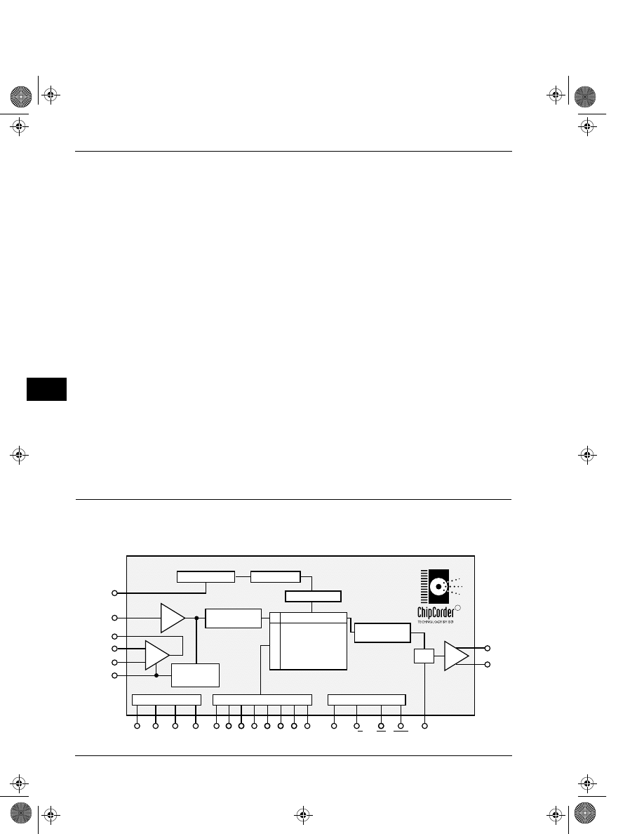
The ISD1000A ChipCorder Series devices are
designed to Record and Play back audio and
voice information in a single chip with a minimum
of circuit complexity. This compact, easy-to-use,
nonvolatile, low-power solution has been made
possible by ISD's multilevel storage technology —
a breakthrough in storage technology in EEPROM.
ISD’s multilevel storage technology results in stor-
age density that is eight times greater than digital
memory. The ISD1000A nonvolatile analog array
consists of 128K cells — the equivalent of 1 Mbits
of digital storage.
The ISD1000A Series eliminates the need for dig-
ital conversion, digital compression, and voice
synthesis techniques which often compromise
voice quality and are more complicated to use.
The ISD1000A Series includes signal conditioning
circuits and control functions which enable a com-
plete, high-quality Recording and Playback sys-
tem in a single device. The ISD1000A is available
in two versions, which store voice in 16- or 20-sec-
ond arrays. Additional devices may be cascaded
ISD1000A SERIES BLOCK DIAGRAM
Amp
Timing
Internal Clock
Pre-
Amp
V
CCA
V
CCD
Power Conditioning
A0
A2 A3 A4 A5
A7
A6
Address Buffers
ANA IN
ANA OUT
MIC
MIC REF
AGC
Analog Transceivers
Decoders
128 K Cell
Nonvolatile
Multilevel Storage
Array
Amp
Sampling Clock
PD
P/R
CE
EOM
Device Control
XCLK
AUX IN
SP+
SP–
Mux
V
SSA
V
SSD
A1
Automatic
Gain Control
(AGC)
5-Pole Active
Antialiasing Filter
5-Pole Active
Smoothing Filter
R
06.DataBook_1000A Dsht Page 2 Friday, September 27, 1996 10:44 AM
Product Data Sheets
ISD1000A Series
1–3
1
to achieve longer recording durations. The non-
volatile storage array is based on production-
proven, low-power CMOS EEPROM technology.
The highly integrated ISD1000A Series contains
all the basic functions required for high-quality
voice Recording and Playback. The noise-cancel-
ling Microphone Preamplifier and Automatic Gain
Control (AGC) record both low-volume and high-
volume sounds. The AGC attack and release
times are adjusted by an external resistor and
capacitor. Antialiasing is performed by a continu-
ous fifth-order Chebyshev filter, requiring no exter-
nal components or clocks to give toll-quality
reproduction. The low corner of the passband is
user-settable by two external capacitors. The
devices contain their own temperature-stabilized
timebase oscillator.
The ISD1000A devices drive a speaker directly
through differential outputs. This boosts power by
four times and eliminates the need for a series
capacitor or an output amplifier. The device will
operate from a single power supply or from batter-
ies. The device also includes a power down func-
tion for applications where minimum power
consumption is critical. The CMOS-based design,
combined with the nonvolatile storage array,
assures the lowest possible overall power con-
sumption.
On-chip control functions make the ISD1000A
Series very easy to use in a wide array of applica-
tions. Each device offers a variety of operating
modes and interface options. The devices may be
used in applications that require little more than a
few switches and a battery. The devices may also
be integrated into electronic systems where digital
addresses can be provided for more sophisti-
cated message addressing and control. The
ISD1000A array is organized into 160 segments.
Addresses A0 through A7 provide access to each
segment in the array for message addressing.
Addressing provides the capability of construct-
ing messages by combining stored phrases and
sounds.
PIN DESCRIPTIONS
Voltage Inputs (V
CCA
, V
CCD
)
To minimize noise, the analog and digital circuits
in the ISD1000A Series devices use separate
power busses. These voltage busses are brought
out to separate pins and should be tied together
as close to the supply as possible. In addition,
these supplies should be decoupled as close to
the package as possible.
Ground Inputs (V
SSA
, V
SSD
)
The ISD1000A Series of devices utilizes separate
analog and digital ground busses. These pins
should be tied together as close to the package
as possible and connected through a low-imped-
ance path to power supply ground.
Power Down Input (PD)
When not recording or playing back, the PD pin
should be pulled HIGH to place the part in a very
low power mode (see I
SB
specification). When
EOM pulses LOW for an overflow condition, PD
should be brought HIGH to reset the address
pointer back to the beginning of the Record/Play-
back space.
SSD
SSA
M0/A0
M1/A1
M2/A2
M3/A3
M4/A4
M5/A5
NC
NC
A6
A7
AUX IN
V
V
SP+
V
P/R
XCLK
EOM
PD
CE
NC
ANA OUT
ANA IN
AGC
MIC REF
MIC
V
SP–
CCD
CCA
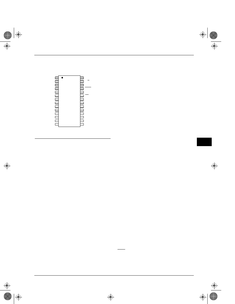
DIP/SOIC
1
2
3
4
5
6
7
8
9
10
11
12
13
14
28
27
26
25
24
23
22
21
20
19
18
17
16
15
ISD1000A SERIES PINOUTS
06.DataBook_1000A Dsht Page 3 Friday, September 27, 1996 10:44 AM
Product Data Sheets
ISD1000A Series
1–4
-
1
Chip Enable Input (CE)
The CE pin is taken LOW to enable all Playback
and Record operations. The address inputs and
Playback/Record input (P/R) are latched by the
falling edge of CE. When CE is taken HIGH, the
ISD1000A is unselected, the P/R is HIGH, and the
auxiliary input is directed into the speaker ampli-
fier.
Playback/Record Input (P/R)
The P/R input is latched by the falling edge of the
CE pin. A HIGH level selects a Playback cycle
while a LOW level selects a Record cycle. For a
Record cycle, the address inputs provide the
starting address and recording continues until PD
or CE is pulled HIGH or an overflow is detected
(i.e. the chip is full). When a Record cycle is termi-
nated by pulling PD or CE HIGH, an End-Of-Mes-
sage (EOM) marker is stored at the current
address in memory. For a Playback cycle, the
address inputs provide the starting address and
the device will play until an EOM marker is
encountered. The device can continue past an
EOM marker in an operational mode, or if CE is
held LOW in address mode. (See page 1-6 for
more Operational Modes).
End-Of-Message Output (EOM)
A non-volatile marker is automatically inserted at
the end of each recorded message. It remains
there until the message is recorded over. During
Playback, the EOM output pulses LOW for a
period of T
EOM
at the end of each message, or in
the event of a message overflow (device full).
In addition, the ISD1000A Series has an internal
V
CC
detect circuit to maintain message integrity
should V
CC
fall below 3.5V. In this case, EOM
goes LOW and the device is fixed in Playback-
only mode. The EOM marker provides a conve-
nient handshake signal for a processor, and also
facilitates the cascading of devices.
Microphone Input (MIC)
The microphone input transfers its signal to the
on-chip preamplifier. An on-chip Automatic Gain
Control (AGC) circuit controls the gain of this
preamplifier from -15 to 24 dB. An external micro-
phone should be AC coupled to this pin via a
series capacitor. The capacitor value, together
with the internal 10 Kohm resistance on this pin,
determines the low-frequency cutoff for the
ISD1000A Series passband. See ISD’s Applica-
tion Notes and Design Manual in this book for
additional information on low-frequency cutoff cal-
culation.
Microphone Reference Input (MIC REF)
The MIC REF input is the inverting input to the
microphone preamplifier. This provides a noise-
canceling or common-mode rejection input to the
device when connected to a differential micro-
phone.
IF
THIS
INPUT
IS
UNUSED
,
IT
MUST
BE
LEFT
DISCONNECTED
.
Automatic Gain Control Input (AGC)
The AGC dynamically adjusts the gain of the
preamplifier to compensate for the wide range of
microphone input levels. The AGC allows the full
range of whispers to loud sounds to be recorded
with minimal distortion. The “attack” time is deter-
mined by the time constant of a 5 K
Ω
internal
resistance and an external capacitor (C2) con-
nected from the AGC pin to V
SSA
analog ground.
The “release” time is determined by the time con-
stant of an external resistor (R2) and an external
capacitor (C2 on the schematic on page 1-17)
connected in parallel between the AGC Pin and
V
SSA
analog ground. Nominal values of 470 K
Ω
and 4.7
µ
F give satisfactory results, in most cases.
For AGC voltages of 1.5V and below, the pream-
plifier is at its maximum gain of 24 dB. Reduction
in preamplifier gain occurs for voltages of approx-
imately 1.8V.
06.DataBook_1000A Dsht Page 4 Friday, September 27, 1996 10:44 AM
Product Data Sheets
ISD1000A Series
1–5
1
Analog Output (ANA OUT)
This pin provides the preamplifier output to the
user. The voltage gain of the preamplifier is deter-
mined by the voltage level at the AGC pin. It has a
maximum gain of about 24 dB for small input sig-
nal levels.
Analog Input (ANA IN)
The analog input pin transfers its signal to the chip
for recording. For microphone inputs, the ANA
OUT pin should be connected via an external
capacitor to the ANA IN pin. This capacitor value,
together with the 2.7 K
Ω
input impedance of ANA
IN, is selected to give additional cutoff at the low-
frequency end of the voice passband. If the
desired input is derived from a source other than
a microphone, the signal can be fed, capacitively
coupled, into the ANA IN pin directly.
Optional External Clock Input (XCLK)
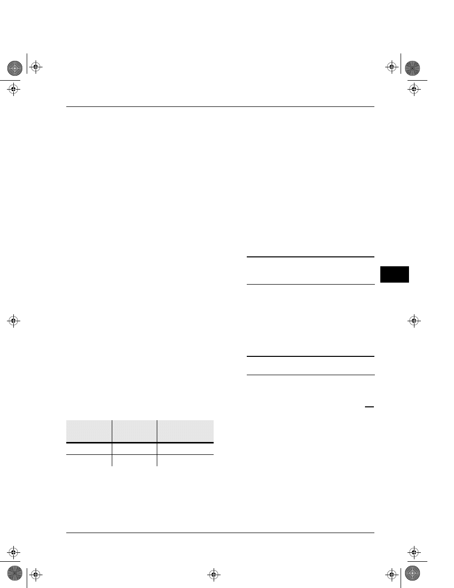
ISD1000A devices are configured at the factory
with an internal sampling clock frequency cen-
tered to
±
1% of specification. The frequency is
maintained to a total variation of
±
2.25% toler-
ance over the entire commercial temperature and
4.5 to 5.5 voltage ranges. The internal clock has a
±
5% tolerance over the industrial temperature
range and 4.5 to 5.5 voltage range. A regulated
power supply is recommended for industrial-tem-
perature-range parts. If greater precision is
required, the device can be clocked through the
XCLK pin as follows.
These recommended clock rates should not be
varied because the antialiasing and smoothing fil-
ters are fixed, and aliasing problems can occur if
the sample rate differs from the one recom-
mended. The duty cycle on the input clock is not
critical, as the clock is immediately divided by
two.
IF
THE
XCLK
IS
NOT
USED
,
THIS
INPUT
MUST
BE
CONNECTED
TO
GROUND
.
Speaker Outputs (SP+/SP-)
All devices in the ISD1000A Series include an on-
chip differential speaker driver, capable of driving
50 milliwatts into 16
Ω
from AUX IN (12.2 mW from
memory).
The speaker outputs are held at V
SSA
levels during
record and power down. It is therefore not possi-
ble to parallel speaker outputs of multiple
ISD1000A devices or the outputs of other speaker
drivers.
NOTE
Connection of speaker outputs in parallel
may cause damage to the device.
While a single output may be used alone (includ-
ing a coupling capacitor between the SP pin and
the speaker), these outputs may be used individ-
ually with the output signal taken from either pin.
Using the differential outputs results in a 4:1
improvement in output power.
NOTE
Never ground or drive an output.
Auxiliary Input (AUX IN)
The Auxiliary Input is multiplexed through to the
output amplifier and speaker output pins when CE
is HIGH and Playback has ended, or if the device
is in overflow. When cascading multiple ISD1000A
devices, the AUX IN pin is used to connect a Play-
back signal from a following device to the
previous output speaker drivers. For noise consid-
erations, it is suggested that the Auxiliary Input not
be driven when the storage array is active.
Address/Mode Inputs (Ax/Mx)
The Address/Mode Inputs provide two functions in
the ISD1000A Series: 1. Message address (either
Part
Number
Sample Rate
Required Clock
ISD1016A
8.0 KHz
1024 KHz
ISD1020A
6.4 KHz
819.2 KHz
06.DataBook_1000A Dsht Page 5 Friday, September 27, 1996 10:44 AM
Product Data Sheets
ISD1000A Series
1–6
-
1
A6 or A7 = LOW) and 2. ISD1000A Series Opera-
tional Mode Options (A6 AND A7 = HIGH).
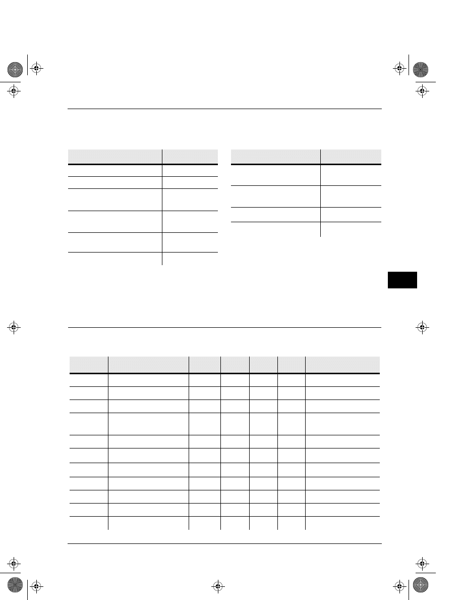
Operational mode options are shown in the Oper-
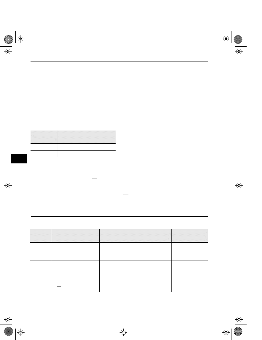
ational Modes table. There are a maximum of 160
message addresses (or segments). Each seg-
ment corresponds to one of 160 rows in the ana-
log storage array. The message addresses
(segments) are in locations 0 through 159 contig-
uous. The playback/record duration of each seg-
ment depends upon the device and is as follows:
An operation may be started at any address, as
defined by address pins A0-A7. Record or play-
back continues with automatic incrementing of the
internal on-chip address until either CE is brought
HIGH (Record), an end of message marker is
encountered (Playback with CE HIGH), or an over-
flow (device full) condition results.
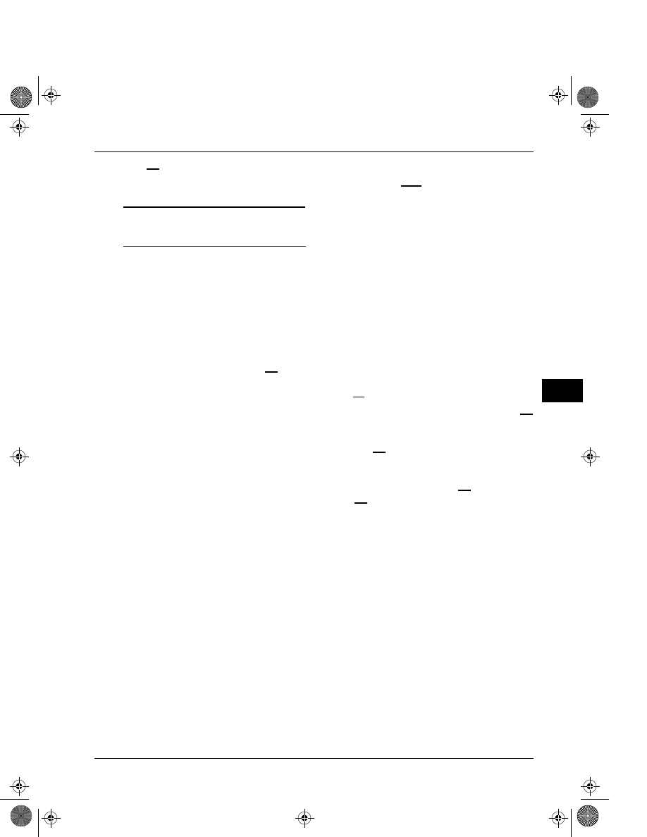
OPERATIONAL MODES
The ISD1000A Series is designed with several
built-in operational modes provided to allow max-
imum functionality with a minimum of additional
components, described in detail below. The oper-
ational modes use the address pins on the
ISD1000A devices, but are mapped outside the
valid address range. When the two Most Signifi-
cant Bits (MSBs) are HIGH (A6 = A7=1), the
remaining address signals are interpreted as
mode bits and
NOT
as address bits. Therefore,
operational modes and direct addressing are not
compatible and cannot be used simultaneously.
There are two important considerations for using
operational modes. First, all operations begin ini-
tially at address 0, which is the beginning of the
ISD1000A address space. Later operations can
begin at other address locations, depending on
the operational mode(s) chosen. In addition, the
address pointer is reset to 0 when the device is
changed from Record to Playback, or when a
Power-Down cycle is executed.
Second, an Operational Mode is executed when
CE goes LOW and the two MSBs are HIGH. This
Operational Mode remains in effect until the next
Part
Number
Segment Playback/Record
Duration
ISD1016A
100 milliseconds
ISD1020A
125 milliseconds
Control
Mode
Function
Typical Use
Jointly Compatible*
M0
Message cueing
Fast-forward through messages
M4, M5
M1
Delete EOM markers
Position EOM marker at the end of the last
message
M3, M4, M5
M2
Cascading
Adding devices to extend message
M3
Looping
Continuous playback from Address 0
M1, M5
M4
Consecutive addressing
Record/Play multiple consecutive mes-
sages
M0, M1, M5
M5
CE level-activated
Allow message pausing
M0, M1, M3, M4
OPERATIONAL MODES TABLE
NOTE:
An asterisk (*) indicates additional operational modes which can be used simultaneously with the given mode.
06.DataBook_1000A Dsht Page 6 Friday, September 27, 1996 10:44 AM
Product Data Sheets
ISD1000A Series
1–7
1
LOW-going CE signal, at which point the current
address/mode levels are sampled and executed.
NOTE
The two MSBs are on pins 9 and 10 for
each ISD1000A Series member.
OPERATIONAL MODES DESCRIPTION
The Operational Modes can be used in conjunc-
tion with a microcontroller, or they can be hard-
wired to provide the desired system operation.
M0 — Message Cueing
Message Cueing allows the user to skip through
messages, without knowing the actual physical
addresses of each message. Each CE LOW
pulse causes the internal address pointer to skip
to the next message. This mode should be used
for Playback only, and is typically used with the
M4 Operational Mode.
M1 — Delete EOM Markers
The M1 Operational Mode allows sequentially
recorded messages to be combined into a single
message with only one EOM marker set at the end
of the combined message. When this operational
mode is configured, messages recorded sequen-
tially are played back as one continuous mes-
sage.
M2 — Used for Cascading
During playback, EOM goes LOW at array over-
flow only. Normal EOM pulses are turned off.
M3 — Message Looping
The M3 Operational Mode allows for the auto-
matic, continuously repeated playback of the
message located at the beginning of the address
space. A message
CANNOT
completely fill the
ISD1000A device and loop.
M4 — Consecutive Addressing
During normal operations, the address pointer will
reset when a message is played through to an
EOM marker. The M4 Operational Mode inhibits
the address pointer reset on EOM, allowing mes-
sages to be played back consecutively.
M5 — CE Level Activated
The default mode for ISD1000A devices is for CE
to be edge-activated on Playback and level-acti-
vated on Record. The M5 Operational Mode
causes the CE pin to be interpreted as level-acti-
vated as opposed to edge-activated during Play-
back. This is specifically useful for terminating
Playback operations using the CE signal. In this
mode, CE LOW begins a Playback cycle at the
beginning of device memory.
06.DataBook_1000A Dsht Page 7 Friday, September 27, 1996 10:44 AM
1–8
Product Data Sheets
ISD1000A Series
-
1
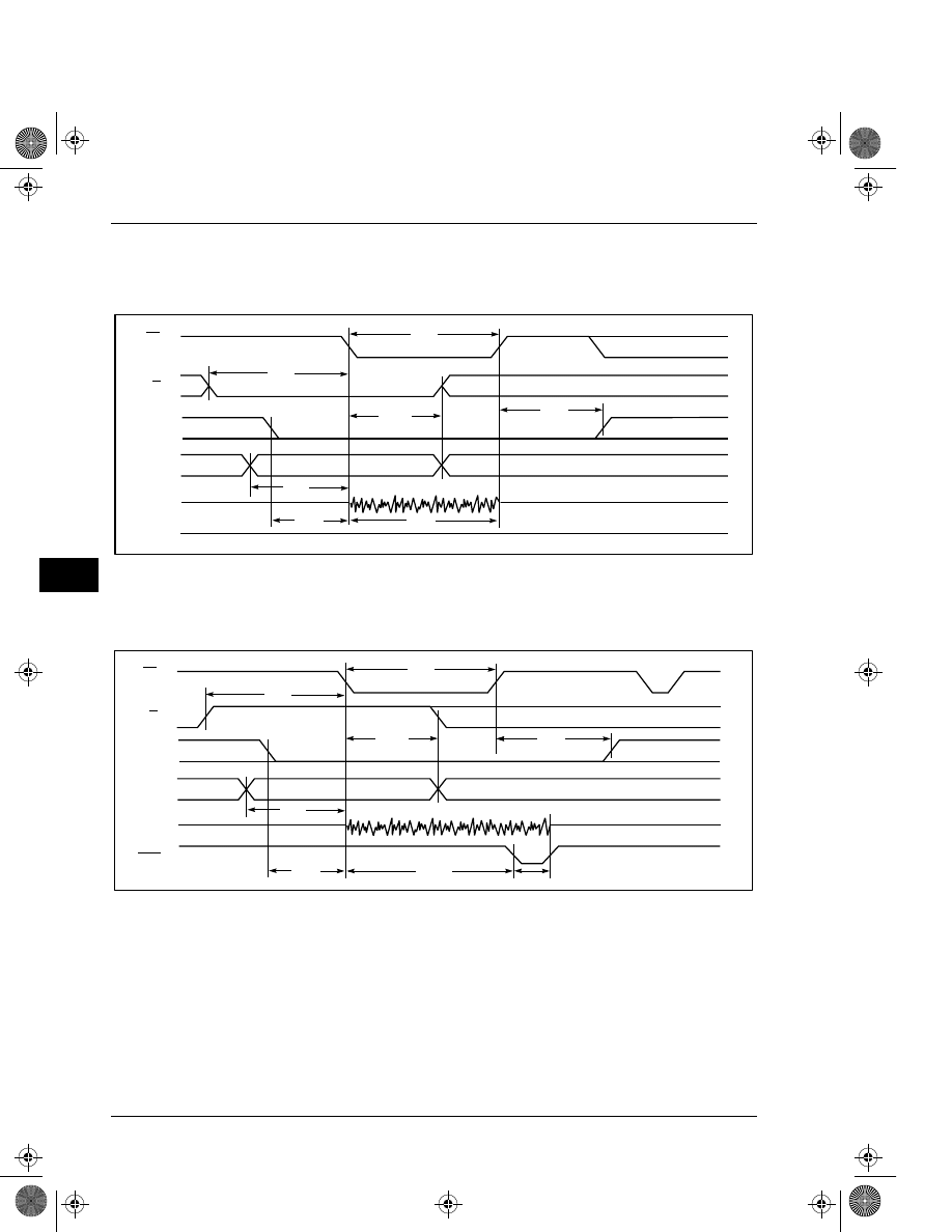
TIMING DIAGRAMS
Record
Playback
A0-A7
CE
Mic
Ana In
T
CE
T
PDH
T
SET
T
HOLD
SP+/-
PD
T
PUD
Don't Care
Don't Care
Don't Care
Don't Care
T
SET
P/R
T
REC
Don't Care
A0-A9
CE
T
CE
T
SET
T
HOLD
PD
SP+/–
EOM
T
PUD
T
EOM
Don't Care
Don't Care
Don't Care
Don't Care
T
SET
P/R
T
PDH
T
PLAY
Don't Care
MIC
ANA IN
A0-A7
06.DataBook_1000A Dsht Page 8 Friday, September 27, 1996 10:44 AM
Product Data Sheets
ISD1000A Series
1–9
1
ABSOLUTE MAXIMUM RATINGS
(PACKAGED PARTS)
NOTE:
Stresses above those listed may cause permanent
damage to the device. Exposure to the absolute
maximum ratings may affect device reliability.
Functional operation is not implied at these
conditions.
Condition
Value
Junction temperature
150
°
C
Storage temperature range
–65
°
C to +150
°
C
Voltage applied to any pin
(V
SS
– 0.3 V) to
(V
CC
+ 0.3 V)
Voltage applied to any pin (Input
current limited to
±
20 mA)
(V
SS
– 1.0 V) to
(V
CC
+ 1.0 V)
Lead temperature (soldering –
10 seconds)
300
°
C
V
CC
- V
SS
– 0.3 V to + 7.0 V
OPERATING CONDITIONS
(PACKAGED PARTS)
NOTES: 1.
Case temperature.
2.
V
CC
= V
CCA
= V
CCD
.
3.
V
SS
= V
SSA
= V
SSD
.
Condition
Value
Commercial operating
temperature range
(1)
0
°
C to +70
°
C
Industrial operating
temperature
(1)
–40
°
C to +85
°
C
Supply voltage (V
CC
)
(2)
+4.5 V to +5.5 V
Ground voltage (V
SS
)
(3)
0 V
DC PARAMETERS (PACKAGED PARTS)
Symbol
Parameters
Min
(2)
Typ
(1)
Max
(2)
Units
Conditions
V
IL
Input Low Voltage
0.8
V
V
CC
= 4.5 V to 5.5 V
V
IH
Input High Voltage
2.0
V
V
OL
Output Low Voltage
0.4
V
I
OL
= 4.0 mA
V
OH
Output High Voltage
2.4
V
I
OH
= – 1.6 mA,
V
CC
= 4.5 V to 5.5 V
V
OH1
Output High Voltage
V
CC
–0.4
V
I
OH
= – 10
µ
A
I
CC
V
CC
Current (Operating)
25
30
mA
R
EXT
=
∞
(3)
I
SB
V
CC
Current (Standby)
1
10
µ
A
(3)
I
IL
Input Leakage Current
±
1
µ
A
R
EXT
Output Load Impedance
16
Ω
Speaker Load
R
MIC
Preamp In Input Resistance
10
K
Ω
Pins 17, 18
R
AUX
AUX Input Resistance
10
K
Ω
V
CC
= 4.5 V to 5.5 V
06.DataBook_1000A Dsht Page 9 Friday, September 27, 1996 10:44 AM
1–10
Product Data Sheets
ISD1000A Series
-
1
NOTES: 1.
Typical values @ T
A
= 25
°
C and 5.0 V.
2.
All Min/Max limits are guaranteed by ISD via electrical testing or characterization.
Not all specifications are 100% tested.
3.
V
CCA
and V
CCD
connected together.
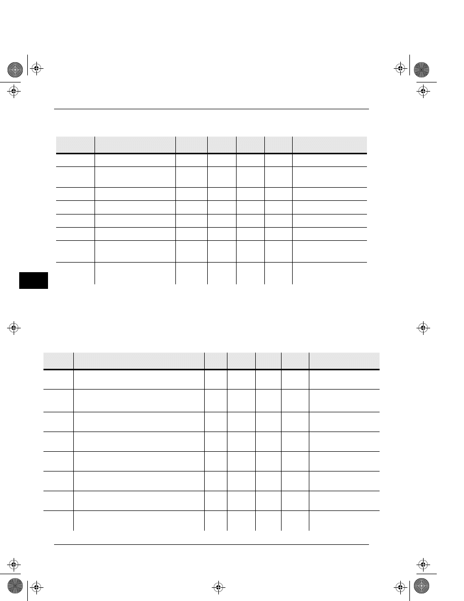
AC PARAMETERS (PACKAGED PARTS)
R
ANA IN
ANA IN Input Resistance
3.0
K
Ω
A
PRE1
Preamp Gain 1
24
dB
AGC = 0.0 V,
V
CC
= 4.5 V to 5.5 V
A
PRE2
Preamp Gain 2
– 45
15
dB
AGC = 2.5 V
A
AUX
AUX IN/ SP+ Gain
0.9
V/V
V
CC
= 4.5 V to 5.5 V
A
ARP
ANA IN to SP+/- Gain
22
dB
R
AGC
AGC Output Resistance
5
K
Ω
I
PREH
Preamp Out Source
– 1
mA
@ V
OUT
= 1.0 V,
V
CC
= 4.5 V to 5.5 V
I
PREL
Preamp In Sink
0.8
mA
@ V
OUT
= 2.0 V,
V
CC
= 4.5 V to 5.5 V
Symbol
Characteristic
Min
(2)
Typ
(1)
Max
(2)
Units
Conditions
F
S
Internal Clock
— ISD1016A
Sampling Frequency
— ISD1020A
8
6.4
KHz
KHz
(9)
(9)
F
CF
Filter Pass Band
— ISD1016A
— ISD1020A
3.4
2.7
KHz
KHz
3 dB Roll-Off Point
(3)(10)
3 dB Roll-Off Point
(3)(10)
T
REC
Record Duration
— ISD1016A
— ISD1020A
16
20
sec
sec
T
PLAY
Playback Duration
— ISD1016A
— ISD1020A
16
20
sec
sec
(9)
(9)
T
CE
CE Pulse Width
— ISD1016A
— ISD1020A
100
100
nsec
nsec
T
SET
Control/Address Setup Time
— ISD1016A
— ISD1020A
300
300
nsec
nsec
T
HOLD
Control/Address Hold Time
— ISD1016A
— ISD1020A
0
0
nsec
nsec
T
PUD
Power-Up Delay
— ISD1016A
— ISD1020A
18.75
31.25
msec
msec
Symbol
Parameters
Min
(2)
Typ
(1)
Max
(2)
Units
Conditions
DC PARAMETERS (PACKAGED PARTS) – CONTINUED
06.DataBook_1000A Dsht Page 10 Friday, September 27, 1996 10:44 AM
1–11
Product Data Sheets
ISD1000A Series
1
NOTES: 1.
Typical values @ T
A
= 25
°
C and 5.0 V.
2.
All Min/Max limits are guaranteed by ISD via electrical testing or characterization. Not all specifications are 100% tested.
3.
Low-frequency cutoff depends upon value of external capacitors (see Pin Descriptions).
4.
From AUX IN; if ANA IN is driven at 50 mV p-p, the POUT= 12.2 mW, typical.
5.
With 5.1 K
Ω
series resistor at ANA IN.
6.
This is the minimum pulse width required to guarantee that a Record cycle will be interrupted. A LOW-going PD pulse
of less than this interval during Record may be ignored.
7.
This is the minimum pulse width required to guarantee that a Playback cycle will be interrupted. A LOW-going PD pulse
of less than this interval during Playback may be ignored.
8.
This is the minimum pulse width required to reset the device when in a static condition; i.e., not actively recording or
playing back.
9.
Sampling Frequency and Playback Duration will vary as much as
±
2.25% over the commercial temperature and voltage
range and
±
5% over the industrial temperature and voltage range. For greater stability, an external clock can be utilized
(see Pin Descriptions).
10.
Filter specification applies to the antialiasing filter and to the smoothing filter.
T
PDR
PD Pulse Width - Record
— ISD1016A
— ISD1020A
25
31.25
msec
msec
(6)
(6)
T
PDP
PD Pulse Width - Play
— ISD1016A
— ISD1020A
12.5
15.625
msec
msec
(7)
(7)
T
PDS
PD Pulse Width - Static
— ISD1016A
— ISD1020A
100
100
nsec
nsec
(8)
(8)
T
PDH
Power Down Hold
— ISD1016A
— ISD1020A
0
0
nsec
nsec
T
EOM
EOM Pulse Width
— ISD1016A
— ISD1020A
12.5
15.6
msec
msec
THD
Total Harmonic Distortion
— ISD1016A
— ISD1020A
1
1
%
%
@ 1 KHz
@ 1 KHz
P
OUT
Speaker Output Power
— ISD1016A
— ISD1020A
12.5
12.5
50
50
mW
mW
R
EXT
= 16
Ω
(4)
R
EXT
= 16
Ω
(4)
V
OUT
Voltage Across Speaker Pins
— ISD1016A
— ISD1020A
2.5
2.5
V p–p
V p–p
R
EXT
= 600
Ω
R
EXT
= 600
Ω
V
IN1
MIC Input Voltage
— ISD1016A
— ISD1020A
20
20
mV
mV
Peak-to-Peak
(5)
Peak-to-Peak
(5)
V
IN2
ANA IN Input Voltage
— ISD1016A
— ISD1020A
50
50
mV
mV
Peak-to-Peak
Peak-to-Peak
V
IN3
AUX IN Input Voltage
— ISD1016A
— ISD1020A
1.25
1.25
V p–p
V p–p
R
EXT
= 16
Ω
R
EXT
= 16
Ω
Symbol
Characteristic
Min
(2)
Typ
(1)
Max
(2)
Units
Conditions
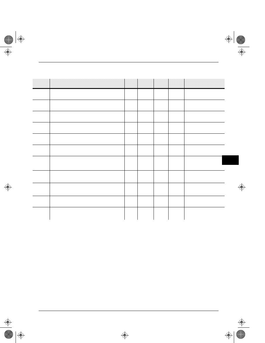
AC PARAMETERS (PACKAGED PARTS) – CONTINUED
06.DataBook_1000A Dsht Page 11 Friday, September 27, 1996 10:44 AM
1–12
Product Data Sheets
ISD1000A Series
-
1
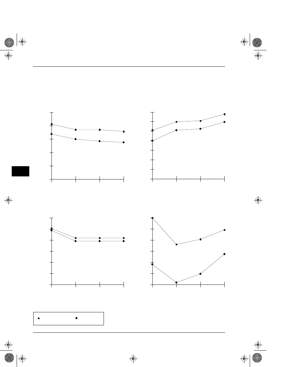
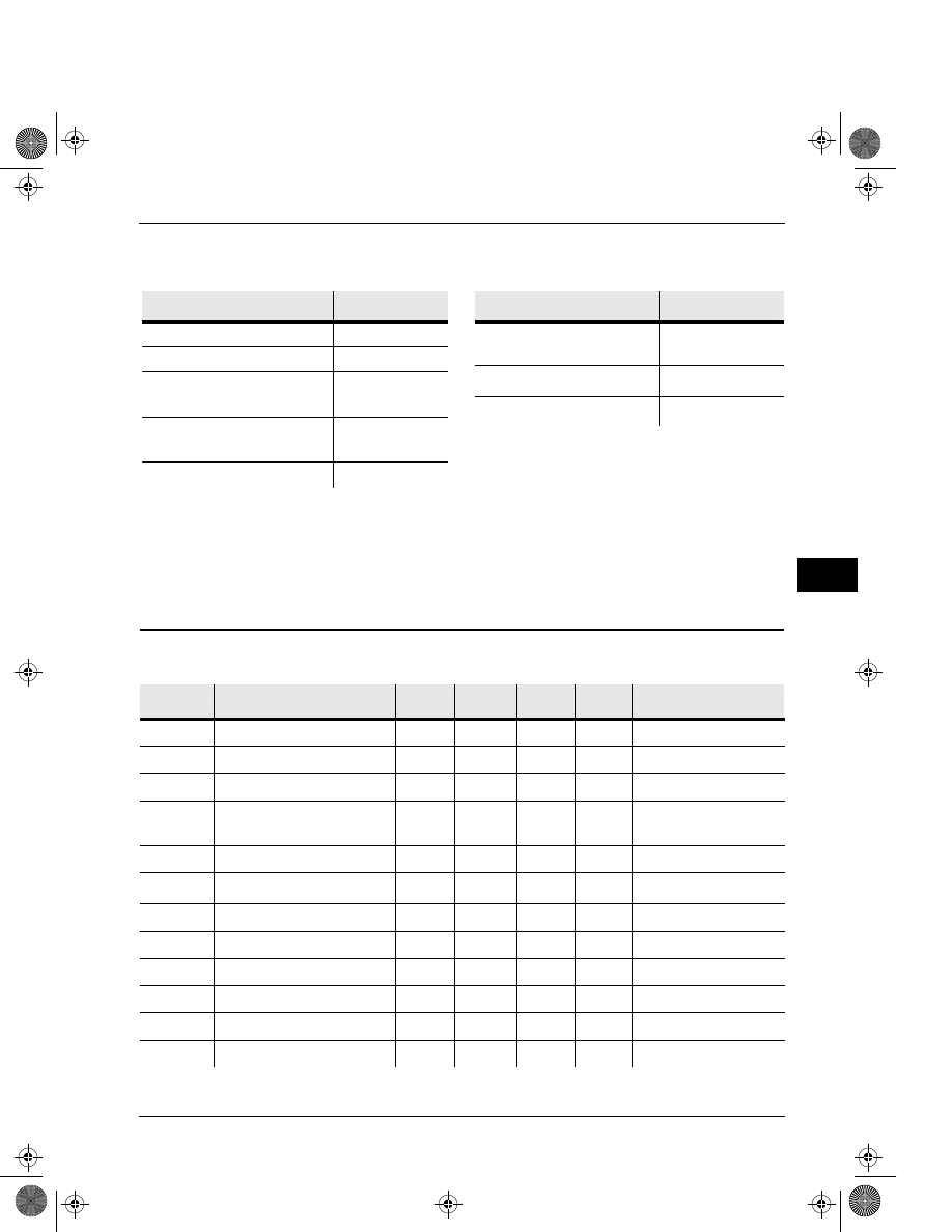
TYPICAL PARAMETER VARIATION WITH VOLTAGE AND TEMPERATURE
(PACKAGED PARTS)
-40
25
20
15
10
5
0
25
70
85
Operating Current (mA)
Temperature (C)
-40
25
70
85
0.7
0.6
0.5
0.4
0.3
0.2
0.1
0
Standb
y Current (
µ
A)
Temperature (C)
-40
1.5
1.0
0.5
0
-0.5
-1.0
-1.5
25
70
85
P
e
rcent Chang
e (%)
Temperature (C)
-40
0.6
0.5
0.4
0.3
0.2
0.1
0
25
70
85
P
e
rcent Distor
tion (%)
Temperature (C)
TOTAL HARMONIC DISTORTION
OSCILLATOR STABILITY
RECORD MODE OPERATING CURRENT (I
CC
)
STANDBY CURRENT (I
SB
)
5.5 Volts
4.5 Volts
06.DataBook_1000A Dsht Page 12 Friday, September 27, 1996 10:44 AM
Product Data Sheets
ISD1000A Series
1–13
1
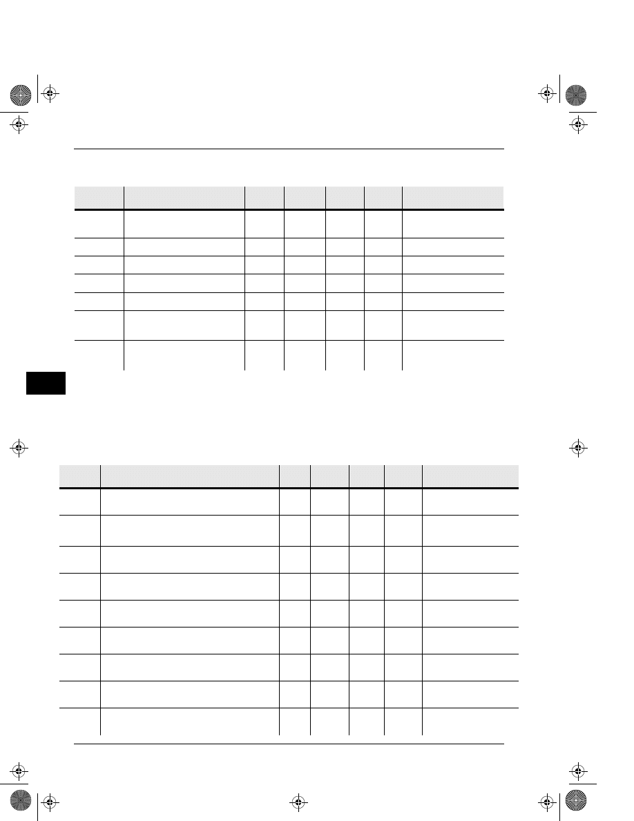
ABSOLUTE MAXIMUM RATINGS (DIE)
NOTE:
Stresses above those listed may cause permanent
damage to the device. Exposure to the absolute
maximum ratings may affect device reliability.
Functional operation is not implied at these
conditions.
Condition
Value
Junction temperature
150
°
C
Storage temperature range
–65
°
C to +150
°
C
Voltage applied to any pad
(V
SS
– 0.3 V) to
(V
CC
+ 0.3 V)
Voltage applied to any pad
(Input current limited to
±
20 mA)
(V
SS
– 1.0 V) to
(V
CC
+ 1.0 V)
V
CC
- V
SS
– 0.3 V to + 7.0 V
OPERATING CONDITIONS (DIE)
NOTES: 1.
Case temperature.
2.
V
CC
= V
CCA
= V
CCD
.
3.
V
SS
= V
SSA
= V
SSD
.
Condition
Value
Commercial operating
temperature range
(1)
0
°
C to +50
°
C
Supply voltage (V
CC
)
(2)
+4.5 V to +6.5 V
Ground voltage (V
SS
)
(3)
0 V
DC PARAMETERS (DIE)
Symbol
Parameters
Min
(2)
Typ
(1)
Max
(2)
Units
Conditions
V
IL
Input Low Voltage
0.8
V
V
CC
= 4.5 V to 5.5 V
V
IH
Input High Voltage
2.0
V
V
OL
Output Low Voltage
0.4
V
I
OL
= 4.0 mA
V
OH
Output High Voltage
2.4
V
I
OH
= –1.6 mA,
V
CC
= 4.5 V to 5.5 V
V
OH1
Output High Voltage
V
CC
–0.4
V
I
OH
= – 10
µ
A
I
CC
V
CC
Current (Operating)
25
30
mA
R
EXT
=
∞
(3)
I
SB
V
CC
Current (Standby)
1
10
µ
A
(3)
I
IL
Input Leakage Current
±
1
µ
A
R
EXT
Output Load Impedance
16
Ω
Speaker Load
R
MIC
Preamp In Input Resistance
10
K
Ω
Pins 17, 18
R
AUX
AUX Input Resistance
10
K
Ω
V
CC
= 4.5 V to 5.5 V
R
ANA IN
ANA IN Input Resistance
3.0
K
Ω
06.DataBook_1000A Dsht Page 13 Friday, September 27, 1996 10:44 AM
Product Data Sheets
ISD1000A Series
1–14
-
1
NOTES: 1.
Typical values @ T
A
= 25
°
C and 5.0 V.
2.
All Min/Max limits are guaranteed by ISD via electrical testing or characterization.
Not all specifications are 100% tested.
3.
V
CCA
and V
CCD
connected together.
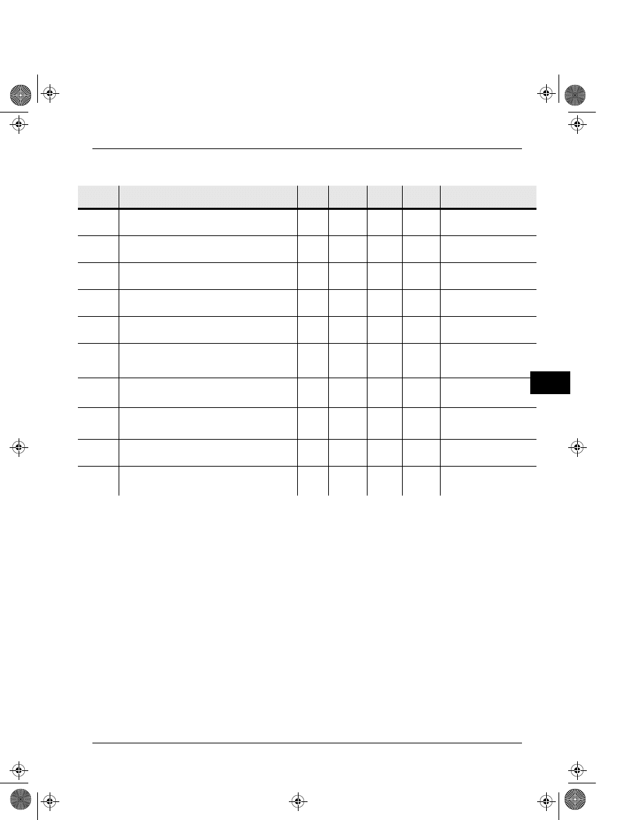
AC PARAMETERS (DIE)
A
PRE1
Preamp Gain 1
24
dB
AGC = 0.0 V,
V
CC
= 4.5 V to 5.5 V
A
PRE2
Preamp Gain 2
– 45
15
dB
AGC = 2.5 V
A
AUX
AUX IN/ SP+ Gain
0.9
V/V
V
CC
= 4.5 V to 5.5 V
A
ARP
ANA IN to SP+/- Gain
22
dB
R
AGC
AGC Output Resistance
5
K
Ω
I
PREH
Preamp Out Source
– 1
mA
@ V
OUT
= 1.0 V,
V
CC
= 4.5 V to 5.5 V
I
PREL
Preamp In Sink
0.8
mA
@ V
OUT
= 2.0 V,
V
CC
= 4.5 V to 5.5 V
Symbol
Characteristic
Min
(2)
Typ
(1)
Max
(2)
Units
Conditions
F
S
Internal Clock
— ISD1016A
Sampling Frequency
— ISD1020A
8
6.4
KHz
KHz
(9)
(9)
F
CF
Filter Pass Band
— ISD1016A
— ISD1020A
3.4
2.7
KHz
KHz
3 dB Roll-Off Point
(3)(10)
3 dB Roll-Off Point
(3)(10)
T
REC
Record Duration
— ISD1016A
— ISD1020A
16
20
sec
sec
T
PLAY
Playback Duration
— ISD1016A
— ISD1020A
16
20
sec
sec
(9)
(9)
T
CE
CE Pulse Width
— ISD1016A
— ISD1020A
100
100
nsec
nsec
T
SET
Control/Address Setup Time
— ISD1016A
— ISD1020A
300
300
nsec
nsec
T
HOLD
Control/Address Hold Time
— ISD1016A
— ISD1020A
0
0
nsec
nsec
T
PUD
Power-Up Delay
— ISD1016A
— ISD1020A
18.75
31.25
msec
msec
T
PDR
PD Pulse Width - Record
— ISD1016A
— ISD1020A
25
31.25
msec
msec
(6)
(6)
Symbol
Parameters
Min
(2)
Typ
(1)
Max
(2)
Units
Conditions
DC PARAMETERS (DIE) – CONTINUED
06.DataBook_1000A Dsht Page 14 Friday, September 27, 1996 10:44 AM
Product Data Sheets
ISD1000A Series
1–15
1
NOTES: 1.
Typical values @ T
A
= 25
°
C and 5.0 V.
2.
All Min/Max limits are guaranteed by ISD via electrical testing or characterization.
Not all specifications are 100% tested.
3.
Low-frequency cutoff depends upon value of external capacitors (see Pin Descriptions).
4.
From AUX IN; if ANA IN is driven at 50 mV p-p, the POUT= 12.2 mW, typical.
5.
With 5.1 K
Ω
series resistor at ANA IN.
6.
This is the minimum pulse width required to guarantee that a Record cycle will be interrupted. A LOW-going PD pulse
of less than this interval during Record may be ignored.
7.
This is the minimum pulse width required to guarantee that a Playback cycle will be interrupted. A LOW-going PD pulse
of less than this interval during Playback may be ignored.
8.
This is the minimum pulse width required to reset the device when in a static condition; i.e., not actively recording or
playing back.
9.
Sampling frequency and Playback duration will vary as much as
±
2.25% over the commercial temperature and voltage
range. For greater stability, an external clock can be utilized (see Pin Descriptions).
10.
Filter specification applies to the antialiasing filter and to the smoothing filter.
T
PDP
PD Pulse Width - Play
— ISD1016A
— ISD1020A
12.5
15.625
msec
msec
(7)
(7)
T
PDS
PD Pulse Width - Static
— ISD1016A
— ISD1020A
100
100
nsec
nsec
(8)
(8)
T
PDH
Power Down Hold
— ISD1016A
— ISD1020A
0
0
nsec
nsec
T
EOM
EOM Pulse Width
— ISD1016A
— ISD1020A
12.5
15.6
msec
msec
THD
Total Harmonic Distortion
— ISD1016A
— ISD1020A
1
1
%
%
@ 1 KHz
@ 1 KHz
P
OUT
Speaker Output Power
— ISD1016A
— ISD1020A
12.5
12.5
50
50
mW
mW
R
EXT
= 16
Ω
(4)
R
EXT
= 16
Ω
(4)
V
OUT
Voltage Across Speaker Pins
— ISD1016A
— ISD1020A
2.5
2.5
V p–p
V p–p
R
EXT
= 600
Ω
R
EXT
= 600
Ω
V
IN1
MIC Input Voltage
— ISD1016A
— ISD1020A
20
20
mV
mV
Peak-to-Peak
(5)
Peak-to-Peak
(5)
V
IN2
ANA IN Input Voltage
— ISD1016A
— ISD1020A
50
50
mV
mV
Peak-to-Peak
Peak-to-Peak
V
IN3
AUX IN Input Voltage
— ISD1016A
— ISD1020A
1.25
1.25
V p–p
V p–p
R
EXT
= 16
Ω
R
EXT
= 16
Ω
Symbol
Characteristic
Min
(2)
Typ
(1)
Max
(2)
Units
Conditions
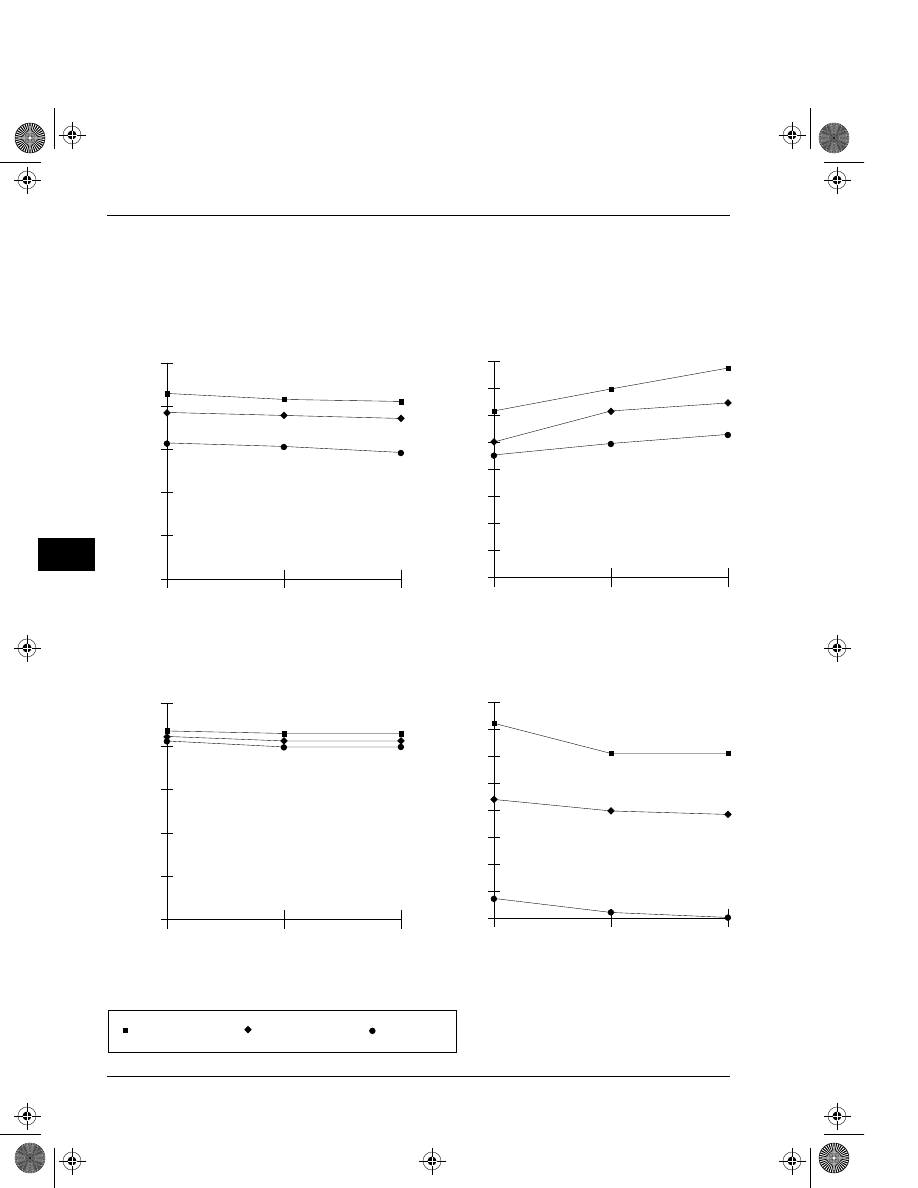
AC PARAMETERS (DIE) – CONTINUED
06.DataBook_1000A Dsht Page 15 Friday, September 27, 1996 10:44 AM
1–16
Product Data Sheets
ISD1000A Series
-
1
TYPICAL PARAMETER VARIATION WITH VOLTAGE AND TEMPERATURE (DIE)
0.5
0.4
0.3
0.2
0.1
0
0
25
50
0
25
50
-1.5
2.5
1.5
1.0
0.5
0
-0.5
-1.0
2.0
25
20
15
10
5
0
0
25
50
0
25
50
0
0.8
0.6
0.5
0.4
0.3
0.2
0.1
0.7
6.5 Volts
5.5 Volts
4.5 Volts
Operating Current (mA)
Temperature (C)
Standb
y Current (
µ
A)
Temperature (C)
P
e
rcent Chang
e (%)
Temperature (C)
P
e
rcent Distor
tion (%)
Temperature (C)
TOTAL HARMONIC DISTORTION
OSCILLATOR STABILITY
RECORD MODE OPERATING CURRENT (I
CC
)
STANDBY CURRENT (I
SB
)
06.DataBook_1000A Dsht Page 16 Friday, September 27, 1996 10:44 AM
1–17
Product Data Sheets
ISD1000A Series
1
SSD
SSA
A0
A1
A2
A3
A4
A5
A6
A7
CE
PD
P/R
EOM
XCLK
V
V
V
V
SP+
SP–
AUX IN
ANA IN
ANA OUT
MIC REF
MIC
AGC
CCD
CCA
C3
16
Ω
SPEAKER
1
2
3
4
5
6
9
10
23
24
27
25
26
28
16
12
13
14
15
11
20
21
18
17
19
ELECTRET
MICROPHONE
0.1
µ
F
CC
V
CC
V
22
µ
F
SS
V
PLAYBACK/RECORD
POWER DOWN
CHIP ENABLE
ISD1016A/1020A
0.1
µ
F
0.1
µ
F
C5
0.1
µ
F
Mic Ref
C1
0.1
µ
F
CC
V
C2
4.7
µ
F
470 K
Ω
R2
1 K
Ω
R1
10 K
Ω
R3
C4
220
µ
F
(Note)
R
5
5.1 K
Ω
10 K
Ω
R4
C7
C6
C8
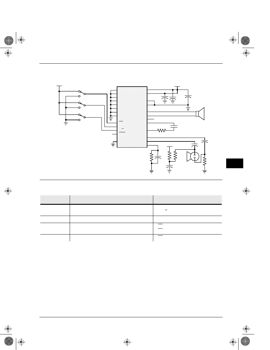
APPLICATION EXAMPLE – DESIGN SCHEMATIC
APPLICATION EXAMPLE – BASIC DEVICE CONTROL
Control Step
Function
Action
1
Power up chip and select record/playback mode
1. PD = LOW
2. P/R = As desired
2
Set message address for record/playback
Set addresses A0–A7
3
Begin playback/record
CE = Pulsed LOW (Playback)
CE = Held LOW (Record)
4
End cycle
CE = HIGH and EOM reached
NOTE:
If desired, pin 18 may be left unconnected
(microphone preamplifier noise will be higher). In this
case, pin 18 must not be tied to any other signal or
voltage.
Additional design example schematics are provided in
the Application Notes and Design Manual in this book.
06.DataBook_1000A Dsht Page 17 Friday, September 27, 1996 10:44 AM
Product Data Sheets
ISD1000A Series
1–18
-
1
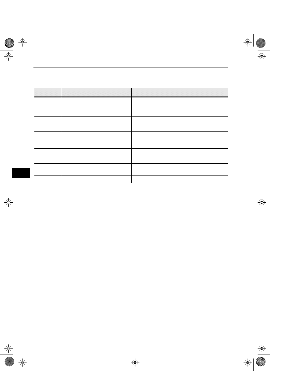
APPLICATION EXAMPLE – PASSIVE COMPONENT FUNCTIONS
Part
Function
Comments
R1
Microphone power supply
decoupling
Reduces power supply noise
R2
Release time constant
Sets release time for AGC
R3, R4
Microphone biasing resistors
Provides biasing for microphone operation
R5
Series limiting resistor
Reduces level at high supply voltages
C1, C5
Microphone DC–blocking capacitor
Low-frequency cutoff
Decouples microphone bias from chip. Provides
single-pole low-frequency cutoff and common-mode
noise rejection
C2
Attack/Release time constant
Sets attack/release time for AGC
C3
Low-frequency cutoff capacitor
Provides additional pole for low-frequency cutoff
C4
Microphone power supply
decoupling
Reduces power supply noise
C6, C7, C8
Power supply capacitors
Filter and bypass of power supply
06.DataBook_1000A Dsht Page 18 Friday, September 27, 1996 10:44 AM
1–19
Product Data Sheets
ISD1000A Series
1
ISD1000A Series
Duration:
16 = 16 Seconds
20 = 20 Seconds
Special Temperature Field:
Blank
= Commercial Packaged (0˚C to +70˚C)
or Commercial Die (0˚C to +50˚C)
I = Industrial (-40˚C to +85˚C)
Package Type:
G
= 28-Lead 0.350-Inch Small Outline Integrated Circuit
(SOIC)
P
= 28-Lead 0.600-Inch Plastic Dual In-Line Package
(PDIP)
X
= Die
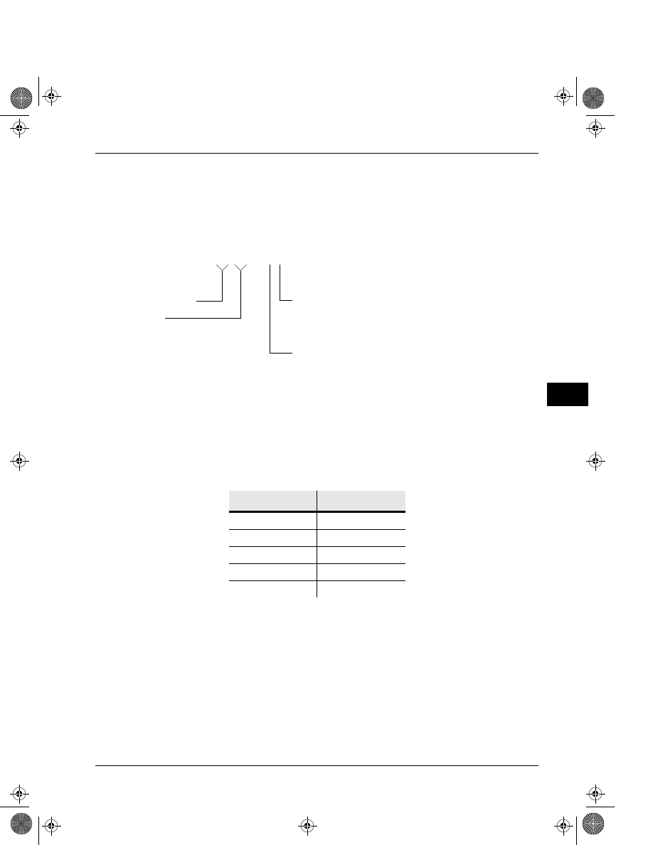
ORDERING INFORMATION
Part Number
Part Number
ISD1016AG
ISD1020AG
ISD1016AGI
ISD1020AGI
ISD1016AP
ISD1020AP
ISD1016API
ISD1020API
ISD1016AX
ISD1020AX
ISD10 _ _ A _ _
Product Number Descriptor Key
When ordering ISD1000A Series devices, please refer to the following valid part numbers.
For the latest product information, access ISD’s worldwide website at http://www.isd.com.
06.DataBook_1000A Dsht Page 19 Friday, September 27, 1996 10:44 AM
1–20
Product Data Sheets
ISD1000A Series
-
1
06.DataBook_1000A Dsht Page 20 Friday, September 27, 1996 10:44 AM
Document Outline
- Features
- General Description
- Detailed Description
- Pin Descriptions
- Voltage Inputs (VCCA, VCCD)
- Ground Inputs (VSSA, VSSD)
- Power Down Input (PD)
- Chip Enable Input (CE)
- Playback/Record Input (P/R)
- End-Of-Message Output (EOM)
- Microphone Input (MIC)
- Microphone Reference Input (MIC REF)
- Automatic Gain Control Input (AGC)
- Analog Output (ANA OUT)
- Analog Input (ANA IN)
- Optional External Clock Input (XCLK)
- Speaker Outputs (SP+/SP-)
- Auxiliary Input (AUX IN)
- Address/Mode Inputs (Ax/Mx)
- Operational Modes
- Operational Modes Description
- Absolute Maximum Ratings (Packaged Parts)
- Operating Conditions (Packaged Parts)
- DC Parameters (Packaged Parts)
- AC Parameters (Packaged Parts)
- NOTES: 1. Typical values @ TA = 25° C and 5.0 V.
- 2. All Min/Max limits are guaranteed by ISD via el...
- 3. Low-frequency cutoff depends upon value of exte...
- 4. From AUX IN; if ANA IN is driven at 50 mV p-p, ...
- 5. With 5.1 K½ series resistor at ANA IN.
- 6. This is the minimum pulse width required to gua...
- 7. This is the minimum pulse width required to gua...
- 8. This is the minimum pulse width required to res...
- 9. Sampling Frequency and Playback Duration will v...
- 10. Filter specification applies to the antialiasi...
- Absolute Maximum Ratings (Die)
- Operating Conditions (Die)
- DC Parameters (Die)
- AC Parameters (Die)
- NOTES: 1. Typical values @ TA = 25° C and 5.0 V.
- 2. All Min/Max limits are guaranteed by ISD via el...
- 3. Low-frequency cutoff depends upon value of exte...
- 4. From AUX IN; if ANA IN is driven at 50 mV p-p, ...
- 5. With 5.1 K½ series resistor at ANA IN.
- 6. This is the minimum pulse width required to gua...
- 7. This is the minimum pulse width required to gua...
- 8. This is the minimum pulse width required to res...
- 9. Sampling frequency and Playback duration will v...
- 10. Filter specification applies to the antialiasi...
- ISD1000A Series
- ISD1000A Series Block Diagram
- ISD1000A Series Pinouts
- Typical Parameter Variation with Voltage and Tempe...
- Timing Diagrams
- Playback
- Application Example – Design Schematic
- Typical Parameter Variation with Voltage and Tempe...
- Ordering Information
- Operational Modes Table
- Application Example – Basic Device Control
- Application Example – Passive Component Functions
- ISD1000A Series Summary
Wyszukiwarka
Podobne podstrony:
nagrywanie dzwieku id 313007 Nieznany
Abolicja podatkowa id 50334 Nieznany (2)
4 LIDER MENEDZER id 37733 Nieznany (2)
katechezy MB id 233498 Nieznany
metro sciaga id 296943 Nieznany
perf id 354744 Nieznany
interbase id 92028 Nieznany
Mbaku id 289860 Nieznany
Probiotyki antybiotyki id 66316 Nieznany
miedziowanie cz 2 id 113259 Nieznany
LTC1729 id 273494 Nieznany
D11B7AOver0400 id 130434 Nieznany
analiza ryzyka bio id 61320 Nieznany
pedagogika ogolna id 353595 Nieznany
Misc3 id 302777 Nieznany
cw med 5 id 122239 Nieznany
D20031152Lj id 130579 Nieznany
więcej podobnych podstron