Warp Speed, Mr.
magine your desktop computer running at the
speed of light. Sure, the electrons that are
switches sitting on a bed of silicon really slow the works down. Rev those up
to the speed of light as well, and you’ll have a real screamer on your hands.
Fantasy? Not necessarily, and you’ll have your chance to help make it
a reality.
We first ran an article on the photonic transistor about a
half ago that described this new little wonder and some of its potential. Now
we go the next step in our first article this month and look at its potential for
use in full-blown computers. Many problems remain to be worked out, so
Intel doesn’t have to worry about the Pentium quite yet, but
when these little
holograms
become real, they could change the face of computing. Find out
what work is being done and how you can get involved.
I’m particularly fond of our second article because I was there when the
germ of the idea was planted. I first saw the original
at the
Exploritorium while I was visiting Shaun with some other college buddies
about seven years ago. Since then, we’ve both built
(though
mine pales in comparison) and I’ve had feedback from other Circuit Cellar
readers about their own experiences with the concept after they saw the
Wavy Sign, one of our Honorable Mentions in the Fifth Annual Circuit Cellar
Design Contest (by the way, this article was already in the works when that
contest entry came in, so it was a complete coincidence). Take a look and
have some fun.
Do you automatically fill in the interrupt vector table when you sit down
to develop a new embedded project? Are interrupts a way of life, no matter
what you’re trying to do? If so, you may want to rethink your philosophy.
Depending on what you’re trying to do, living without them can make your
life much easier, as our third article tries to show.
Next, the great debate over whether to use assembly language or a
high-level language continues, but what about a compromise? Our last
feature article describes a programming technique that combines the best of
both into a discipline that many would do well to adopt.
In our columns, Ed continues talking about how to add a large LCD
panel to his Firmware Development system with a discussion of the
hardware. Jeff adds some smarts to the new
thermostat chip to
make a networkable, intelligent thermostat. Tom crosses enemy lines into
the analog camp to look at some new chips that are bound to give the
venerable op-amp a run for its money. John introduces a new series in
which he’ll be describing how to build a general-purpose embedded control
system based on a compact backplane. Finally, Russ looks at patents that
deal with our theme of Applications in Light.
CIRCUIT CELLAR
THE COMPUTER
APPLICATIONS
JOURNAL
FOUNDER/EDITORIAL DIRECTOR
Steve Ciarcia
EDITOR-IN-CHIEF
Ken Davidson
TECHNICAL EDITOR
Michael Swartzendruber
ASSOCIATE EDITOR
Rob
ENGINEERING STAFF
Jeff Bachiochi Ed Nisley
WEST COAST EDITOR
Tom
CONTRIBUTING EDITORS
John Dybowski Russ Reiss
NEW PRODUCTS EDITOR
Harv Weiner
PUBLISHER
Daniel
PUBLISHER’S ASSISTANT
Susan McGill
CIRCULATION COORDINATOR
Rose
CIRCULATION ASSISTANT
Barbara
CIRCULATION CONSULTANT
Gregory Spitzfaden
BUSINESS MANAGER
Jeannette Walters
ADVERTISING COORDINATOR
Dan Gorsky
CIRCUIT CELLAR INK, THE COMPUTER
J O U R N A L
IS
monthly by Circuit Cellar Incorporated, 4 Park Street,
ART DIRECTOR
Lisa Ferry
20, Vernon, CT 06066 (203)
Second
One-year 2
rate U S.A. and
GRAPHIC ARTIST
Joseph Quinlan
tries $49.95. All subscription orders payable U.S.
funds only,
postal money order or
check drawn on U.S. bank. Direct
orders
and subscription related
to The Computer
Journal
P.O. Box 7694,
NJ 06077 or call (609)
POSTMASTER: Please send address changes to The
CONTRIBUTORS:
Jon
Tim
Frank Kuechmann
Pellervo Kaskinen
Cover Illustration by Bob Schuchman
PRINTED IN THE UNITED STATES
Applications Journal,
Dept., P.O.
Box
7634,
NJ 06077
ASSOCIATES
NATIONAL ADVERTISING REPRESENTATIVES
NORTHEAST
SOUTHEAST
Debra Andersen
Collins
WEST COAST
Barbara Jones
(617) 769-8950
Fax: (617) 769-8982
MID-ATLANTIC
Barbara Best
(305) 966-3939
Fax: (305) 985-8457
MIDWEST
Nanette Traetow
Shelley Rainey
(714)
Fax: (714)
(908) 741-7744
Fax: (908) 741-6823
(708) 789-3080
Fax: (708) 789-3082
1
9600 bps
HST. (203)
All programs and schematics in Circuit Cellar
been carefully
to
their performance
transfer by subscribers
no warranties and
for errors
programs or schematics or the consequences of any such errors. Furthermore, because of
the
and condition of
and
of reader-assembled projects.
Cellar
INK
disclaims any
for the safe and proper function of reader-assembled projects based upon or from
plans,
or
published in
Cellar
INK.
Entire contents copyright 1994 by
Cellar Incorporated. All
reserved
of
whole or
consent from
Cellar is prohibited
2
Issue
February 1994
The Computer Applications Journal
1 4
Programmable
to Develop Photonic
Products for Fun and Profit
by
2 6
In the Eye of the Beholder/Displaying
Messages
with the
II
by Shaun Greaney
3 6
Interrupt-free Design
by Do- While Tones
4 0
An Assembly Language Programming Aid
by Hank Wallace
386SX Project’s Bitmapped
Ed Nisley
5 8
q
From the Bench
Warming Up the Digital Thermostat
Bachiochi
6 4
q
Silicon Update
Op-amp Terminators
Tom Can
q
Embedded Techniques
Data Logging and Collection Devices
Dybowski
Letters to the Editor
New Product News
edited by Harv Weiner
Excerpts from
the Circuit Cellar BBS
conducted by
Ken Davidson
Steve’s Own INK
Steve Ciarcia
And the Survey Says...
Advertiser’s Index
The Computer Applications Journal
Issue
February 1994
Not Quite So Basic Temperature Control
with certain computer systems, but I can’t find anyone
The “Home Temperature Control Basics” article in
who sells one for my vehicle. I think this is a very good
the January ‘94 issue was a fine analytical presentation. I
area for future articles in your magazine.
enjoyed the analysis as well as the insight provided. I
Second, I am trying to get started in building my
would like to ask that the author consider the significant
own virtual reality system at home. I have LCD shutter
energy savings that can be obtained by using electronic
glasses for stereo viewing. I can’t seem to find anyone
adjustable-speed drives
to control the speed of
who sells them for less than
$150
each. Is there anyone
motors that operate fans, blowers, and centrifugal
out there who manufactures just the glass alone? In
pumps; that is, variable-torque loads.
other words, would it be cheaper for me to build my own
The power to be saved over other flow control
instead of paying someone else to do something I am
methods such as louvers, dampers, flow restrictors,
quite confident in doing myself. The trouble is finding
bypass valves, and so forth is described by the cube of
the original source (again at a reasonable cost]. Edmund
the reduced flow rate. For example, a 20% flow
Scientific sells this sort of material but the smallest size
tion using dampers for a fan would make the motor work
they sell is 6” x 6”-far too big for glasses.
harder and in no way reduce required horsepower,
Thanks.
whereas speed/flow reduction using an ASD produces
the following:
=
+ 0.05 =
Bert Schneider
We added the 5% to account for electrical
Colorado Springs, CO
losses in the drive. This principle is the basis for the
electric utility rebate programs that are designed to
encourage energy conservation and annually save
millions of kilowatt hours.
While we’ll never publish a “special index issue,” we do
For references, refer to “Adjustable Speed Drives
get a lot of requests for an article index. An index is an
Directory,” third edition, from the Electric Power
on-going project that we are working on as time permits,
Research Institute, and “Electrical Engineering Pocket
so there is no way of knowing when we’ll have
Handbook,” 1993, from Electrical Apparatus Service
thing completed (there is a lot of information in five
Association. Thank you again for the fine article.
years’ worth of issues). In the meantime, one of the
users of the Circuit Cellar BBS has put together a list
Joe Foster
Fairport, N.Y.
(via the Circuit Cellar BBS)
that could be used as a makeshift index. The file is
posted in the file area.
Your first question comes up on the BBS several
times a year, but we have yet to hear any concrete
answer to it. The auto manufacturers appear to keep a
tight grip on the technical details on their on-board
Virtual Car Computer Request
computers, giving it only to diagnostic tool
ers under nondisclosure. Plenty of people have been
I
have been a devoted subscriber to your journal
quick to provide the meanings of the “blink” codes used
since its inception. Keep up the good work. While I
by come cars, but the amount of information that can
might not have time to go through everything, I
be gleaned from those is woefully inadequate. If any of
tainly use your product as a good reference from time to
our readers can provide more information, we’ll pass it
time. Have you thought of publishing a special index
along to everyone.
issue that gives a quick reference by subject, author, and
As for your second question, we can’t provide any
other categorical information?
good answers here. Again, perhaps one of our readers
Anyway, I have just two questions I would like to
can shed
some
light.
pose to you, your staff, or perhaps some readers. First,
where can
I
get information about the diagnostic codes
and electrical interfaces on Ford computers? I bought a
‘93 Probe GT and I can’t find anyone with this informa-
tion. I know there are third-party vendors who sell
Giving Pitch Correction a KISS
computer interface devices and software for personal
Regarding the “Pitch Correction” discussion in the
computers to perform diagnostic tests on cars equipped
January ‘94 installment of
Many years
6
Issue
February 1994
The Computer Applications Journal
ago I read about an invention developed at Bell Labs, I
Contacting Circuit Cellar
believe, to prevent audio feedback in public-address
We at the Computer
Journal encourage
systems.
communication between our readers and our staff, so have made
The principle was to shift the audio pitch by 5 Hz
every effort to make contacting us easy. We prefer electronic
(cycles in those days) so the auditorium peak feedback
communications, but feel free to use any of the following:
frequency could not be sustained. The pitch change of 5
cycles (oops, Hertz) would be imperceptible by most ears.
Mail:
Letters to the Editor may be sent to: Editor, The Computer
The technique was to beat the audio up to an RF
Applications Journal, 4 Park St., Vernon, CT 06066.
frequency by a local oscillator (to 455
I think) and
Phone:
Direct all subscription inquiries to (609) 786-0409.
then demodulate it with another oscillator running Hz
Contact our editorial offices at (203) 875-2199.
lower or higher.
Fax:
All faxes may be sent to (203)
A similar principle can be observed while listening
BBS:
All of our editors and regular authors frequent the Circuit
to SSB (single sideband) AM radio. Tuning the receiver
Cellar BBS and are available to answer questions. Call
off of the center frequency changes the pitch drastically
(203) 871-1988 with your modem
bps,
up or down. I seems to me that there is a simpler
Internet:
Electronic mail may also be sent to our editors and
solution here that is less hardware/software intensive
regular authors via the Internet. To determine a particular
than using a DSP or CCD.
person’s Internet address, use their name as it appears in
the masthead or by-line, insert a period between their first
Warren L. Graves
and last names, and append
to the end.
Georgetown,
For example, to send Internet
to Jeff Bachiochi,
address it to
For more
information, send
to
The BEST in ROM
emulation technology:
Mbit
includes a day,
no-risk money back guarantee!
Call Today 800-776-6423
Grammar
Engine
Inc.
921
Dr., Suite 122
OH 4308 1
Fax
04
The Computer Applications Journal
Issue
February 1994
7
Edited by Harv Weiner
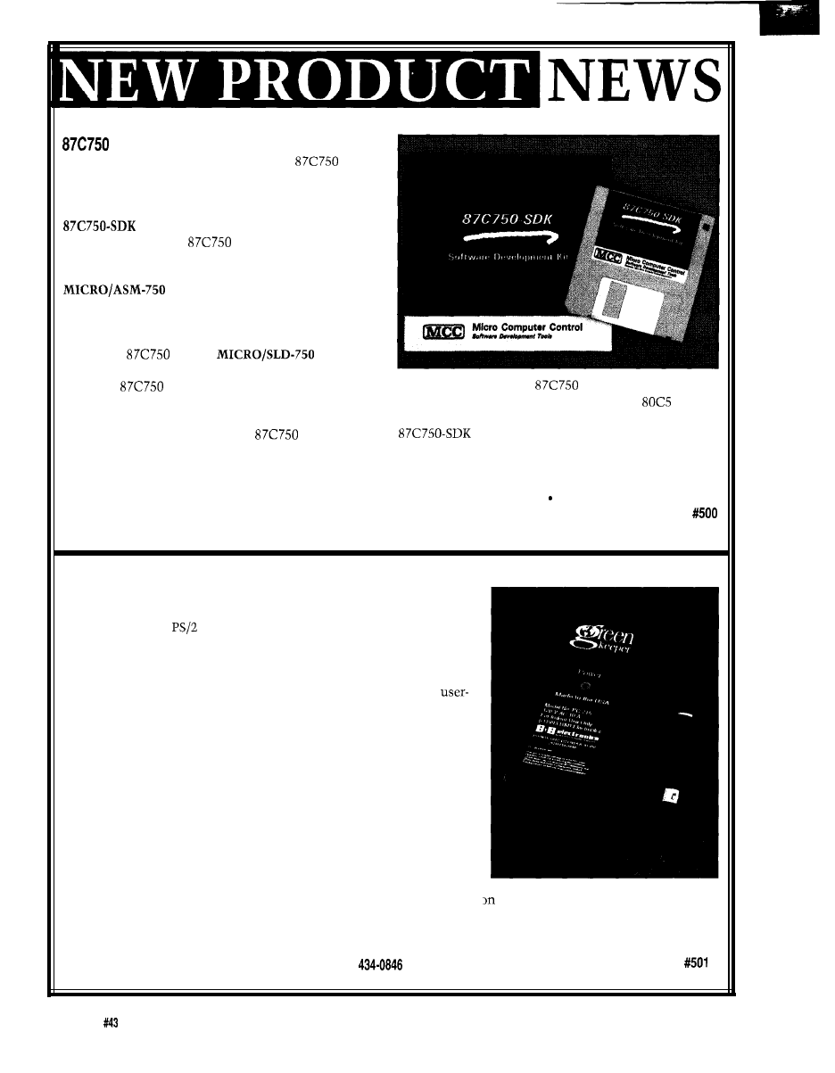
MICROCONTROLLER DEVELOPMENT KIT
Developers working with the Philips
microcontroller can now get a low-cost, feature-packed
tool set in a new software development kit available
from Micro Computer Control Corporation. The
contains all the tools needed to create,
assemble, and execute
programs.
MICRO/EDITOR is a full-featured, multiwindow
text editor for creating and editing source programs.
is a macro assembler that creates a
robust programming environment that quickly finds and
reports source file syntax errors, generates detailed
program listings, and converts a source program into
executable
format.
is a
simulator and source language debugger that can be used
to
execute
programs directly on a PC without
any additional hardware.
This DOS-based development package has been
specially configured to support an
target proces-
sor environment, including memory spaces, peripheral
ports, and timers. Also supported is a source debug
environment including instruction single-stepping,
breakpoints, watch windows, and over 17 additional
tools.
Applications for the
include consumer and
industrial products that can benefit from its
1
architecture, small package size, and low cost. The
is available until April 1994 for an intro-
ductory price of $39.95. The regular list price is $99.95.
Micro Computer Control Corp.
P.O. Box 275.17 Model Ave. Hopewell, NJ 08525
(609) 466-l 751
l
Fax: (609) 466-4116
ENERGY SAVING DEVICE FOR PCS
A low-cost hardware device for reducing the energy consumption of
PC-compatible and
personal computer peripherals has been an-
nounced by B&B Electronics. The
Green
Keeper connects to the keyboard
of any PC. A monitor, printer, modem, or other peripheral can be plugged
into Green Keeper’s AC outlet. The software inlcuded with the system
allows users to set the unit to turn off connected peripherals after a
specified period of inactivity. A simple touch of the keyboard or mouse
restores power to the monitor and peripherals. The CPU is not affected.
The main application of Green Keeper is to reduce the energy con-
sumption of computing. According to the Environmental Protection
Agency, 40 percent of the computer monitors in the U.S. are left on all the
time; each of these monitors generates up to $114 in electric bills per year.
Green Keeper cuts these costs by turning off monitors or other peripherals
in a way that’s simple and convenient for the user.
Green Keeper is contained in a 4.7” x 2” x 1.4” package and can handle
a maximum load of 10 amps. Software is available for DOS, Windows 3.1,
and OS/2 2.1. A Macintosh version is planned for release in early 1994. In
keeping with environmental responsibility, the unit is packaged with
100% recycled and recyclable materials, and the software and documentatic
sells for $69.95 and comes with a three-year warranty.
is on recycled disks. Green Keeper
B&B Electronics Mfg. Co.
4000 Baker Rd.
l
P.O. Box 1040, Ottawa, IL 61350 . (815)
. Fax: (815) 434-7094
8
Issue
February 1994
The Computer Applications Journal
DIRECT READING TEMPERATURE SENSOR
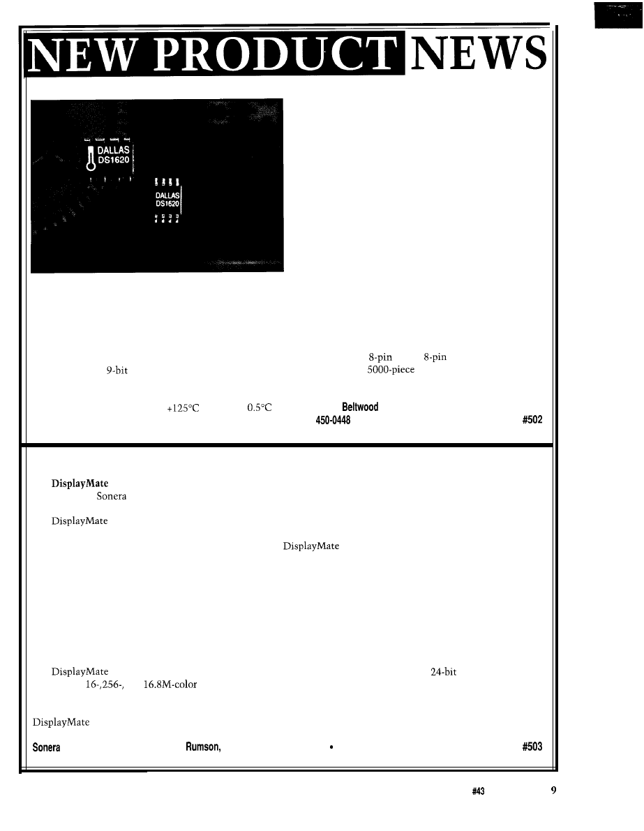
Dallas Semiconductor has announced an all-digital
temperature sensor. Unlike other devices, which output
an analog voltage that must be converted to a digital
value, the DS1620 Digital Thermometer and Thermostat
does direct digital temperature conversion. Temperature
is converted to a
digital number in less than one
second.
Fully calibrated at the factory, the DS1620 features
0.5” resolution over a -55°C to
range and
accuracy in the 0°C to 70°C range. Existing devices can
achieve this kind of accuracy only if they are calibrated
in the end application.
The DS 1620 can also function as a stand-alone
thermostat with two user-definable and changeable set
points that are stored in nonvolatile memory. For
example, the DS 1620 can eliminate excess power drain
and noise in a portable computer by running the fan only
when it is needed. Other applications for the DS1620
include environmental controls, industrial systems,
consumer products, thermometers, and any thermally
sensitive system.
Existing temperature sensors create a voltage drop
across a nonlinear element and then have an external
A/D converter measure the output. By contrast, the
DS 1620 uses two oscillators whose frequency is deter-
mined by a resistor. The resistor in each oscillator has
different temperature characteristics. The DS1620
determines temperature by comparing the values of the
frequencies from the two oscillators.
The DS 1620 Digital Thermometer and Thermostat
is available in an
DIP or
SOIC package and
sells for $2.50 in
quantities.
Dallas Semiconductor
4401 South
Pkwy.
l
Dallas, TX 75244
(214)
l
Fax: (214) 450-0470
SOFTWARE IMPROVES MONITOR QUALITY
for Windows, a revolutionary software product that improves monitor picture quality, has been
announced by
Technologies. The program is said to improve sharpness and contrast, reduce certain forms of
geometric distortion, minimize or eliminate annoying moire patterns, and improve color and grayscale accuracy.
for Windows works by presenting a slide show of screen images, similar in principle to the test
patterns used by television stations. They have been scientifically designed to search for every possible potential
weakness of a computer monitor at very high sensitivity.
for Windows then shows how to improve the
image, with the eye as the final judge of the results. This product requires no video knowledge and is appropriate for
computer novices and experts alike.
Each screen contains a detailed description that explains “what to look for” and includes detailed step-by-step
instructions on “what you can do” to improve the appearance of the image. In most cases, several different tech-
niques are provided, each with an approach dependent on the nature of the problem and the user controls available
on the monitor and video adapter. As an example of the new and innovative approached taken by the product: some
types of geometric distortion can be reduced or eliminated by using the monitor’s position control together with the
video adapter’s own image position adjustment in an offsetting combination. If the monitor and video adapter don’t
include these controls, alternative methods are suggested.
for Windows supports all color modes from monochrome up through full
color, including
the popular
and
modes. An extensive set of test patterns is provided for evaluating and
exploring color quality, balance, range, and accuracy. For users interested in color matching, a special test pattern is
provided for adjusting and matching both reflective and transmissive color samples using a number of color modes.
for Windows sells for $79.
Technologies
l
P.O. Box 565
l
NJ 07760
l
(908) 747-6886 Fax: (908) 747-4523
The Computer Applications Journal
Issue
February 1994
REAL-TIME CLOCK FEATURES
HIGH ACCURACY
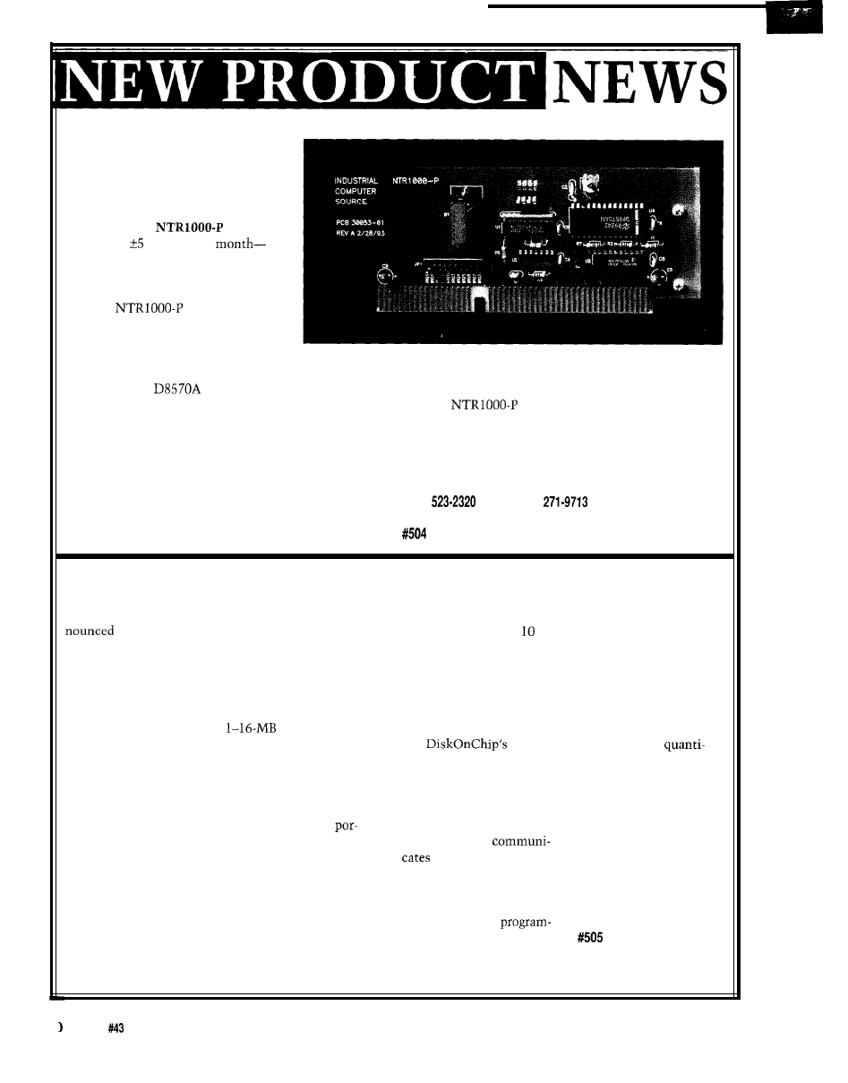
Industrial Computer Source has
announced a low-cost real-time clock
card for IBM PC and compatible
computers. The
provides a
stability of seconds per
better than two-fold improvement over
standard DOS clocks-in harsh
operating environments of 0-50°C.
The
is ideal for
control, test, and measurement
applications requiring a more stable
and accurate clock than is provided
with most DOS systems. The card features the National
network file server, any node on the network has access
Semiconductor
chip with battery-backup power
to highly accurate, stable time.
and is referenced to a stable crystal with a known aging
The
Real-time Clock card sells for
rate. To further enhance precision and accuracy, the
$199.00 and includes the board, manual, and software.
oscillator is calibrated to the normal operating tempera-
ture of the PC for the best reference possible.
Industrial Computer Source
Other features of the card include fO.O1 second
10180 Scripps Ranch Blvd.
accuracy, user-definable automatic update intervals from
San Diego, CA 92131-1298
1 minute to 45% days, extended AT interrupt support, a
(800)
l
Fax: (619)
Novell driver, and a lifetime guarantee. The card is ideal
for use with networks. By installing the card in the
SINGLE-CHIP
hardware reconfiguration is
rate of about 50M bits per
contains the system
FLASH DISK
required. The chip uses the
second, the chip boosts
BIOS, a Flash File
Eurom has an-
embedded Flash File System
productivity by making
System, socket, and
its patented
to emulate the organization
system boot-up time to
PCMCIA services, with
DiskOnChip solid-state,
and management of a
20 times faster than system
the remaining flash
nonvolatile memory chip
standard generic read/write
boot-up from a standard
memory as a formatted
with a capacity of up to
disk device.
mechanical hard drive.
disk.
16 megabytes of
DiskOnChip provides
DiskOnChip also features
The 1 MB version of
unformatted “disk space”
the user with a BIOS and a
interleaving support for fast
the DiskOnChip is
that fits pin-for-pin into a
(unformatted)
write and erase operations.
offered for evaluation at
standard personal
solid-state disk in one-chip
features
$99 per chip in
computer BIOS EPROM
package. By adding a
are possible by using an
ties up to 100. Two- and
socket. The chip is
secondary storage device, it
ASIC chip and circuitry to
four-megabyte versions
targeted for hand-held
frees up a PCMCIA slot for
support flash memory
of the chip are also
and embedded computer
essential communication
programming as well as
available.
designers seeking to add
modules used with
memory and logic blocks.
a bootable storage device,
tables and hand-held
The logic block
Eurom, Inc.
extend battery life, and
computers. The flash
between the system
556 Mowry Ave., Ste. 103
maximize space for
memory operates on only 5
and the memory block,
Fremont, CA 94536
mobile systems.
volts, provides extremely
intercepts the disk boot
(510) 505-9083
The DiskOnChip is a
low battery consumption
routine, and intercepts BIOS
Fax: (510) 505-9084
100 % plug-and-play
compared with a hard drive,
calls during flash
replacement for a system
and requires no battery
ming. The memory block
BIOS chip so that no
backup or maintenance.
contains a minimum of one
additional software or
By using a data transfer
flash memory chip which
Issue
February 1994
The Computer Applications Journal
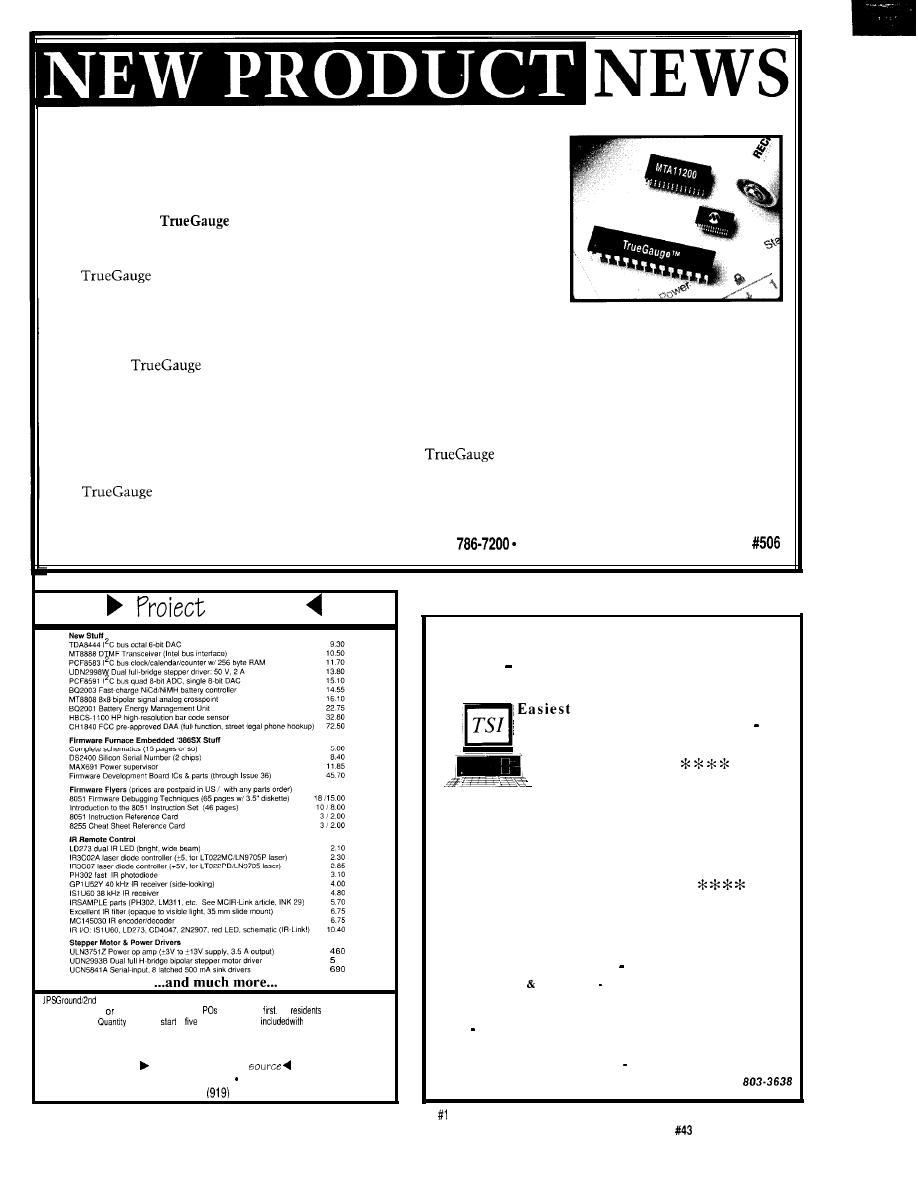
A low-power CMOS integrated circuit that provides
accurate battery monitoring and charging control has
been introduced by the ASSP Division of Microchip
Technology. The
MTA11200
helps predict
imminent battery failure and provides precise real-time
battery capacity measurement and charge control.
BATTERY MONITOR AND CHARGE CONTROL
requests condition-
ing cycles at regular
intervals based on
battery usage, and
can output battery
parameters through a
simple one-wire
transmission link.
Parameters include
remaining capacity,
is designed to operate with either
nickel-cadmium, nickel-metal hydride, or lead-acid
battery packs. It is ideally suited for use in portable
computers, portable video equipment, cellular phones,
and other devices that rely on rechargeable battery
technology.
resides in the battery pack
where it continuously monitors battery condition. It
calibrates itself automatically and continuously,
maintaining a high level of accuracy, and excels in
applications where a battery gauge is required to
prevent an interruption in use or data loss due to
insufficient battery power.
total capacity, voltage, current, and temperature. The
product has been specially designed to avoid errors due
to noise, variations in load current, and deep discharge
situations.
A development system that allows system designers
to design and implement full production battery fuel
gauge products for specific applications is also available.
sells for $3.75 in quantities of 10,000. The
development kit sells for $499.00.
measures the battery’s total capacity
during automatic calibration and factors the data into
the state-of-charge calculation to determine the remain-
ing battery capacity. To extend battery life, Truegauge
Microchip Technology, Inc.
2355 West Chandler Blvd.
l
Chandler, AZ 85224-6199
(602)
Fax: (602) 899-9210
Part5
45
day $6.519 to 48 US states, COD add $4.50. PO Boxes and Canadian orders $6 for USP!
mail Check. MO, COD only. no credit cards
add $50, call
NC
add 6% sales tax
discounts
at
parts. Data sheets
all parts.
Call/write/fax for serious/y tempting catalog...
P u r e U n o b t a i n i u m
Your unusual part5
13109 Old Creedmoor Road Raleigh, NC 27613
FAX/voice
676-4525
Build your own Neural Net!
and Expert System!
E A S Y N E U R A L N E T W O R K S
way to quickly learn about
this fascinating new technology
i n c l u d e s a w o r k i n g N e u r a l N e t w o r k
you can train! $59
EASY EXPERT SYSTEMS
Build your own Expert System in about
one day! Includes 40-Page Knowledge
Engineering Manual, Quick Ref Card
for quick start, and powerful Stock
Market Expert System! $69
BOTH $99 + Includes 3 BIG Catalogs
and FREE Talking Expert System Demo
+ Order now and receive a free copy
of talking PC Therapist usually $64.95
3 Catalogs Demo Disk Send your check for $5
We always pay postage
Please specify disk size or we ship 3.5”
Check, American Express, or P.O. to:
THINKING SOFTWARE, INC.
46-16 65TH PLACE Dept cc201
WOODSIDE, N.Y. 11377 PHONE
(718)
05
The Computer Applications Journal
Issue
February 1994
11
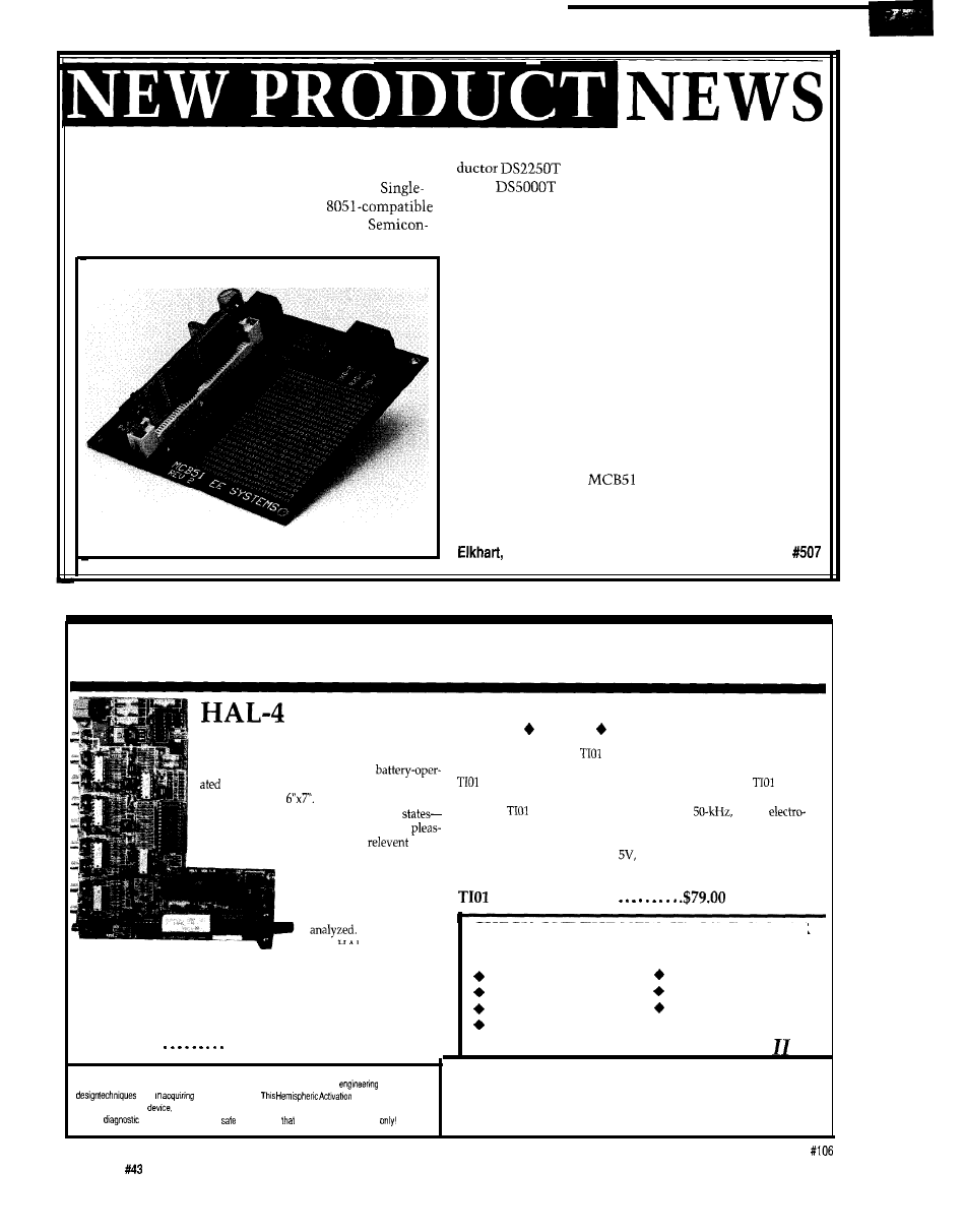
SINGLE-BOARD CONTROLLER
controller, which is the SIP Stik version
EE Systems has announced its new MCB51
of the
DIP package.
board Controller. This easy-to-program
All program and data
memory is contained in
32K
microcontroller board incorporates
the Dallas
bytes of high-speed nonvolatile CMOS RAM. There are
no EPROMs to remove and program. Downloading
applications into the board is accomplished by connect-
ing the board to a DOS PC serial port. An on-chip serial
loader ROM along with a specialized DOS program
(included with the package) makes this downloading
process very quick and easy.
The 3.75” x 3.75” board has all of the standard 8051
features plus 30 I/O lines, a watchdog timer, real-time
clock/calendar, power fail interrupt, and crash-proof
power-down management. A prototyping area is also
included on the board. A free BASIC compiler/assembler,
with several program examples, is also included.
The MCB51 sells for $149.95. A complete C develop-
ment system for the
is also available for $99.95.
EE Systems
50935 Hill Dr.
IN 46514
CIRCUIT CELLAR KITS
Sonar Ranging Experimenter’s Kit
EEG Biofeedback Brainwave Analyzer
Targeting Ranging Machine Vision
The Circuit Cellar
Ultrasonic Sonar Ranger is based on the
The HAL-4 kit is a complete
sonar ranging circuitry from the Polaroid SX-70 camera system. The
I-channel electroencephalograph (EEG) which
and the original SX-70 have similar performance but the
Sonar
measures a mere
HAL is sensitive enough
Ranger requires far less support circuitry and interface hardware.
to even distinguish different conscious
The
ranging kit consists of a Polaroid
300-V
between concentrated mental activity and
static transducer and ultrasonic ranging electronics board made by Texas
ant daydreaming. HAL gathers all
alpha,
Instruments. Sonar Ranger measures ranges of 1.2 inches to 35 feet, has a
beta, and theta brainwave
TTL output when operated on
and easily connects to a parallel
signals within the range of
printer port.
4-20 Hz and presents it in a
serial digitized format that
Sonar Ranger kit.
plus shipping
can be easily recorded or
CHECK OUT THE NEW CIRCUIT CELLAR
HAL’s operation is
straightforward. It samples four channels of analog brainwave data 64
HOME CONTROL SYSTEM
times per second and transmits this digitized data serially to a PC at 4800
bps. There, using a Fast Fourier Transform to determine frequency,
amplitude, and phase components, the results are graphically displayed
in real time for each side of the brain.
HAL-4 kit $179.00
plus shipping
Expandable Network
IR Interface
Digital and Analog I/O
Remote Displays
X-10 Interface
Telephone Interface
Voice
Call and ask about the MCS
l
The Circuit Cellar Hemispheric Activation Level detector is presented as an
example of the
To order the products shown or to receive a catalog,
used
brainwave signals.
Level detector is not a
medically approved
no medical claims are made for this device, and it should not be used for
call:
(203) 875-2751
or fax:
(203) 872-2204
medical
purposes. Furthermore,
use requires
HAL be battery operated
Circuit Cellar Kits
l
4 Park Street
l
Suite 12
l
Vernon, CT 06066
12
Issue
February 1994
The Computer Applications Journal
DEVELOPMENT TOOLS DIRECTORY
The New Motorola Microcontroller Development
Tools Directory, published by MW Media, lists more
than
suppliers of hundreds of development tool
products that support designs using the Motorola
and ‘300 families.
REMOTE CONTROL OF COMPUTER
PERIPHERALS
Charts break down the Motorola microcontroller
family by part numbers and include ROM, RAM, timers,
packaging, and additional comments detailing each chip.
The directory lists all key suppliers of development
tools and products. The
book is composed of
product data sheets and line cards for each product. Each
page describes hardware and software development tools
such as in-circuit emulators, programmers, evaluation
boards, debuggers, compilers, and full development
systems. The publication is free, but there is a $5.00
shipping charge for shipments in the U.S. and an $8.00
shipping charge for international orders.
an infrared wireless data link introduced
by Control Bits Corporation, uses a computer RS-232
serial port to provide wireless communication between
computers and control of peripherals. Specially config-
ured for laptop computers,
provides an infrared
transceiver which attaches to the serial port of each
computer and peripheral to be linked.
An infrared signal carries data between the devices,
provided they are within line of sight. The company
also offers devices which enable the infrared signal to be
transmitted into other rooms and around corners.
is available in several configurations. Its
transceiver can be mounted on an antenna, a telescop-
ing antenna, or be attached to a wire and mounted to a
nearby surface.
operates at up to 9600 bps and
requires 12 VDC. A
adapter is available.
MW Media
Control Bits Corp.
50 W. San Fernando, Ste. 675
l
San Jose, CA 95113
(408)
Fax: (408) 288-4728
8429 Center Dr. N.E.
l
Minneapolis, MN 55432
(612) 783-2157
l
Fax: (612) 783-2160
Memory mapped variables
n
In-line assembly language
option
n
Compile time switch to select
805
I or
n
Compatible with any RAM
or ROM memory mapping
Runs up to 50 times faster than
the MCS BASIC-52 interpreter.
Includes
Technology’s
cross-assembler
hex file
n
Extensive documentation
Tutorial included
l
Runs on IBM-PC/XT or
n
Compatible with all 8051 variants
n
$295.
508-369-9556
FAX 508-369-9549
q
Binary
P.O. Box
Technology, Inc.
l
Carlisle,
MA 01741
ideal for control applications, data acquisition, and test
and measurement. Compact and low in price (the Little
PLC’”
above is
and
these controllers are programmed
with our easy-to-use Dynamic
development system. Our
controllers feature digital
and
relays and so-
lenoid drivers,
serial ports, battery-backed mem-
ory and time/date clock,
keypads, enclosures and more!
from your FAX. Request
catalog
The Computer Applications Journal
Issue
February 1994
FEATURES
Programmable Lightware
In the Eye of the
Beholder
interrupt-free Design
An Assembly Language
Programming Aid
John
Programmable Lightware
How to Develop Photonic
Products for Fun and Profit
puter hardware will
be brought into
existence when more
computer-generated graphics (whether
they be plotted, printed out, or
photographically reproduced) are
assembled with off-the-shelf laser
systems, and sold.
What is a photonic computer? is
a computer made up of photonic
transistors.
A photonic transistor is
essentially a tiny photograph that is
able to perform Boolean logic and
photonic signal amplification. a
photonic computer, photographs
replace silicon, and laser light replaces
electricity.
Computer-generated graphics
produced by applying the laws of
optics can be used to create synthetic
holograms. Transparencies reduced
directly from synthetic holograms can
control light beams just as natural
laws predict. Synthetic holograms
calculated to direct light in a photonic
transistor configuration can be used as
“schematics” to produce real holo-
grams that perform logic and amplifi-
cation of “digital light beams” to form
the equivalent of processors, ROM,
RAM, I/O, and so forth.
14
Issue
February 1994
The Computer Applications Journal
BOTH BEAMS
BOTH BEAMS
O N
O N
ONE BEAM ON
ONE BEAM OFF
ONE BEAM ON
ONE BEAM OFF
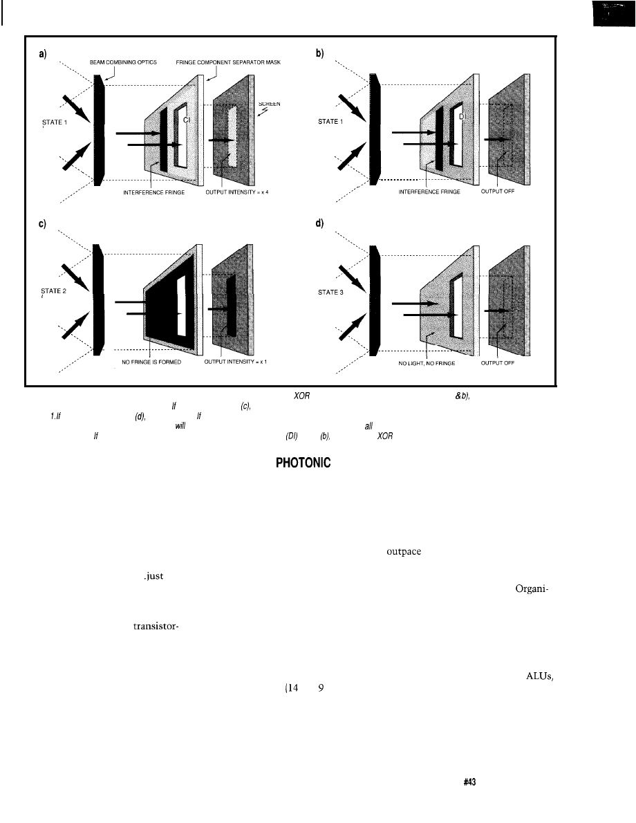
Figure 1-A
simplified photonic transistor showing an amplifier/boolean OR circuit and an
circuit. When two laser beams are combined (a they form an interference
fringe onto a fringe component separating mask. one beam is shut off the fringe goes away and light goes through the hole in the mask to produce an “on” output of
intensity both beams are shut off the output is off. the ho/e in the mask is p/aced at the position of constructive interference (Cl), the output through the hole is four
times the intensity of a sing/e beam.
The device amplify a modulated input signal if the other beam is kept on the time, or it will function as a boolean OR circuit if both
beams are modulated. the hole is p/aced at a position where destructive interference
occurs then a boolean
circuit is produced.
A
great
variety of interconnecting
holograms will be required in a
complete photonic computer, because
the exact holograms needed for each
operation varies from component to
component. Yet, before fully photonic
computers reach the market, myriad
discrete photonic components, each
constructed from a few holograms,
will be developed and sold..
as
was the case with early electronic
products.
Since the holographic components
needed to build photonic
based products are produced by
software, photonic computers and
other devices based on the photonic
transistor are essentially massively
parallel programmable hardware
systems-programmable lightware!
This article explains how to produce
synthetic holograms, as well as the
software related to synthetic hologram
production, for fun and profit.
WHY BUILD A
COMPUTER?
electrons do in semiconductors. Thus,
information is able to be processed at a
Two reasons: speed and money.
Information can be impressed onto
light rays through a variety of tech-
higher speed, using the widest possible
niques. The intelligence-carrying
photons don’t slow down as they pass
through a photonic transistor the way
Naturally, it’s not expected to be
very long before photonic transistor
electrons.
equipment begins to shrink. As the
size goes down, speed goes up. Al-
Before then, macro-sized devices
ready, 3M is able to put 20,000 lenses
in one square centimeter. Photonic
must be produced and tested.
transistors that small will easily
the theoretical limits of
bandwidth.
By way of comparison, a ‘486
running at 66 MHz takes
15
nanosec-
onds per internal clock cycle, and the
latest, hottest, Cray 3 supercomputer
uses 2 ns per cycle. In 2 ns, light
travels 60 cm (23% inches) and in
15
ns, it goes 450 cm
feet inches).
You can fit a whole lot of photonic
transistors in 60 cm, let alone
14 feet!
So, a ‘486
emulated in light, even
using oversized test transistors, would
run faster than a Cray 3.
zational layouts of photonic transistor
arrays have to be designed and opti-
mized. The many details for producing
the massively parallel programmable
synthetic holograms have to be
worked out. And methods for making
registers, processors, memories,
and all of the other structures that
make up computers have to be derived.
Once these steps are complete, the
macro hardware can be scaled down
mathematically to produce full-speed,
optical supercomputers.
The Computer Applications Journal
Issue
February 1994
15
CONNECTION TO ELECTRONIC COMPUTER
ELECTRONIC INTERFACE:
FULL DYNAMIC IMAGE OF
DIGITAL INPUT BEAM MODULATOR(S)
IS
made up
hologram squares that are combined make checkerboard composite holograms.
Each square is part of a
photonic transistor. laser
directed through the holograms produces dynamic images, where the beams from each square blink on and off as digital signals carrying
to
the text
holographic
transistor. Any electronic computer architecture may be
in
way, as a superspeed optical computer.
INTERCONNECTING DIGITAL BEAMS
P H O T O D I O D E
CHECKER BOARD
INPUT
COMPOSITE HOLOGRAMS
This development process has the
distinct advantage that much of the
work can be accomplished using
conventional equipment. Synthetic
holograms sufficient for producing
research and demonstration compo-
nents can be produced on ordinary
computers and printed on VGA or
SVGA screens and laser printers.
These
are then photo-
graphically reduced to become actual
functioning devices. The resulting
holograms can be mounted in a unit
with an off-the-shelf laser to make
functioning photonic products.
The hologram-generating pro-
grams and even the simplest working
photonic products will become very
valuable to hardware hackers and
entrepreneurs involved in photonics.
Educational products are needed so
that developers will be able to keep
abreast of the latest technology. By
using the equipment already available,
programmable lightware provides a
physical means for the production of
actual saleable products.
Yet, there is another very impor-
tant advantage. Programs which
produce holograms can also be used to
test the
holographic
components.
Each
potential photonic product can be
simulated to see how it will function
without having to construct a single
actual component. Thus, photonics
products can be created and tested
without buying a laser or taking even a
single photograph.
Why would you be interested in
producing synthetic holograms on
your own computer? Today, we are on
the ground floor of a new and exciting
technology. Already, long-distance
telephone companies are investing
millions of dollars to switch from
wires to fiber optics.. trading their
electrons for photons, so to speak.
Every experimenter in the world
would like to buy the worlds fastest
components if they were affordable.
Computers made out of photographs
will be less expensive to build than
ones made out of semiconductors. So,
photonic computers can be expected to
outperform and outsell even the best
supercomputers.
There is another very important
reason. We are instituting a “Distrib-
uted Development and Sales Net-
work,” whereby individuals from all
over will be given the opportunity to
share in the development of photonic
components and related software for
sale through our network.
LOGICAL LIGHTWARE
A detailed discussion of photonic
transistor basics is contained in the
August 1992 issue of the
Computer
Applications Journal, so
I will not
duplicate that information here. The
basic concepts needed for this discus-
sion are shown in Figures la and
Two laser beams are brought together
to produce an interference fringe. The
fringe is composed of dark areas of
destructive interference (DI), and
bright areas of constructive interfer-
ence (CI). Photons that ordinarily
would have gone straight towards the
DI area are diverted into the CI area by
the action of interference. Thus, the CI
areas are four times brighter than a
single beam by itself.
How can that be? Let’s compare
Figures la and Ic. A single beam floods
the entire area occupied by the fringe
when both beams are on (Figure lc).
For each photon that lands in the area
that corresponds to the CI area of
Figure la, another lands in the area
that corresponds to the DI area.
Turning on another beam of equal
strength (Figure la) doubles the
number of available photons. So now
we are looking at four photons. Two
headed for the CI area, and two headed
for the DI area. The action of interfer-
ence, though, diverts the photons
headed for the DI area into the CI area.
Thus, where there was one photon in
the CI area with a single beam (Figure
lc), now there are four [Figure la.).
This property is an experimentally
verifiable fact of physics.
16
Issue
February 1994
The Computer Applications Journal
If the component parts of the
fringe are separated using a mask, or
strategically placed holograms, several
functions emerge. Separating the fringe
component parts creates a differential
output between the single beam state
(Figure lc) and the double beam state
(Figure la).
In the example above, the single
beam has two photons and the double
beam has four. Taking the entire com-
bined beam into account, the differen-
tial between having one beam on and
having two beams on is only double
the intensity. Adding the mask drasti-
cally alters that output differential.
With a fringe component separator
that selects only the CI area(s), the
single beam output is cut in half
(Figure lc), whereas the double beam
output remains the same (Figure la). If
both beams are off (Figure
the
output is zero. So, the output switches
from zero photons to one to four as
each beam is turned on. By selecting
different parts from the fringe, differ-
ent computer functions can be pro-
duced.
In Boolean terms, the device is an
OR gate because it produces an “on”
output if either or both input beams
are on. In order to be off, both input
beams must be off. The problem is
that without the mask, light levels (in
the “on” state] fluctuate from one to
two times a single beam intensity, and
with the mask, they fluctuate from
one to four times a single beam
intensity. Fluctuations like that may
cause complications in subsequent
devices.
In actual beams, there are many
photons, and not all of them are
precisely located in the center of the
CI area. If the hole in the mask is
located so as to select photons par-
tially from a CI area and partially from
a DI area, a balance can be found
where the output intensity when both
beams are “on” equals the single beam
state. The result is the OR function
that can be interconnected directly
with other devices.
If the mask separates light from a
DI area (Figure lb), an exclusive-OR
(XOR) device is made. The output
differential switches from zero (Figure
to one (Figure lc) and back to zero
(Figure lc). Since only two functions
are needed to produce everything that
is done on the motherboard of an
electronic computer, every computa-
tion can now be done with light.
If we note the process carefully,
the actual power, or total amount of
light is reduced in the process. That
shouldn’t surprise us. Put your finger
on a ‘486 and consider how much
energy is wasted as heat. Images
generally require much less energy
than a ‘486, so we don’t need
powered lasers. But, light levels will
need to be matched at each stage. So,
an amplification function will be
needed somewhere along the line in
order to be able to interconnect all of
the components properly.
However, many light speed
functions are able to be accomplished
before the on/off contrast reduces to
the point where information is lost.
For example, consider the address
decoding function for a hypothetical
photonic RAM. The entire address
25 MByte
Memory Module
FORMAT
Hard Drive replacement; supports M-Systems
Nonvolatile
memory board
Self Boot mechanism and PC auto detection
Available with up
of storage
Read/write memory system
“Boot Block” of 256KBytes allows DOS in ROM
Byte writable, 64KByte sector erasable
On-board DC to DC convertor for single
volt operation
“The
card allows a system
to boot without mechanical drives,
execute applications and write up to
25MBytes of non-volatile storage.”
ISA FORMAT
For
a list of our international distributors,
please contact our head office at:
“For the OEM with Embedded PC Applications”
megatel”
( 4 1 6 ) 2 4 5 - 2 9 5 3
megatel computer
125
Wendell Ave.
Weston, Ont.
Canada
Fax: (416) 245-6505
The Computer Applications Journal
Issue
February 1994
17
SOLID STATE DISK $135”
Card 2 Disk Emulator
EPROM, FLASH and/or SRAM
Program/Erase FLASH On-Board
Total, Either Drive Bootable
25MHZ 386DX CPU
Compact AT/Bus or Stand Alone
In-Board
IDE, FDC, 2
Drives to
Cache to
DRAM to 48M
TURBO XT
w/FLASH DISK $266”
To 2 FLASH Drives,
Total
DRAM to 2M
FLASH On-Board
CMOS Surface Mount, 4.2” 6.7”
2
Par, Watchdog Timer
Tempustech
products are
PC Bus Compatible. Made in the
30 Day Money Back Guarantee
1, Qty breaks start at pieces.
TEMPUSTECH, INC.
634-0701
Fax for
295 Airport Road
iast response!
Naples, FL 33942
decoding and
read or write
operation is able to take place at the
speed of light, even with each stage in
the process operating at a diminished
power level from the previous stage.
Only on the read function, after the
RAM has been read, must the data bus
be amplified in order to bring it back
up the high levels useful to the
processor.
We have a precedence for this in
electronics. Early computers, and the
internal workings of many computer
chips, use diode-resistor logic for
decoding addresses because they take
up so little space. The output is then
amplified back to TTL levels after the
multistage logic has been performed.
While complete processes may be
created using a descending power
arrangement, amplification will be
needed in order to restore the proper
contrast ratio. There are light amplifi-
ers available on the market, albeit
slow and expensive ones. These could
be used..
why, when we have the
photonic transistor amplifier?
If the mask separates the CI area
(Figure la), and one beam is kept on all
the time, the information on the
modulated beams enters the transistor,
switching from zero intensity (Figure
lc)
to one (Figure
la),
for a contrast
ratio of one. But, it exits switching
from one to four, for an intensity
differential (contrast ratio] of three.
Thus the modulated signal has been
amplified by increasing the contrast
between off and on.
In a comparison to an electronic
amplifier, the beam that remains on, is
like the DC current from the battery.
Without a power supply, the amplifier
quits amplifying. A small modulated
input signal switches the transistor on
and off. The modulated output signal
is larger than the modulated input
signal. It is amplified: its “contrast
ratio” has been increased. Where did
the modulated output signal get the
extra energy! Why, from the battery of
course.
Likewise in photonics, the
constant beam supplies energy to the
modulated beam so that the modu-
lated output beam has more energy
than the modulated input beam, even
though the overall process is less than
Issue
February 1994
The Computer Applications Journal
100% efficient. The same is true of an
electronic transistor.
Many optical beam combining
methods, including some holograms,
block out half of the light from the
input beams. In these cases, power
amplification may be negated, even
though the contrast ratio is amplified.
The increase in contrast will be
sufficient for many applications, but
not for others.
Some of the methods for optimiz-
ing beam-combining optics, so as to
minimize light loss, include the use of
phase holograms and reflecting
holograms such as the ones put on
credit cards. These can be used to
combine beams so as to cause an
actual increase in total light power. As
illustrated above, the amplified output
beam has four photons for every two
photons in the original modulated
beam for a power amplification factor
of two.
Simple photonic transistor
amplification produces a better
contrast ratio, but the output level
remains on at a low level during the
off state. To reduce this constant bias,
the ratio of CI area (that passes
through the mask) to DI area (which is
blocked by the mask) is adjusted so as
to make the CI area as small as
possible and the DI area as large as
possible. Obviously, the
combining optics must create a
matching fringe with a wide DI area
and a narrow CI area. That’s where
holograms come in.
HOLOGRAPHIC
TRANSISTORS
Holograms are able to produce
complex images that can be designed
to produce complex fringes with
predetermined qualities. For example,
a simple zone plate hologram can
increase the contrast ratio by 400
times by focusing the light onto a
small dot much as a magnifying
glass does. When designed to accept
single- and double-beam inputs, the
contrast ratio can really become quite
large.
Holograms are especially useful
for producing differential photonic
amplifiers. A differential amplifier is
similar to a simple amplifier except
that a fringe is produced by the con-
stant bias beam having its CI image
completely blocked by the mask.
When the second beam comes on,
the combined image is calculated so as
to relocate the photons into a second
image that is located elsewhere on the
mask..
that’s where we put the
hole. From another viewpoint, the
constant beam produces a fringe with
its CI area blocked by the mask. When
the second beam comes on, the CI area
of the combined fringe is moved over
to the location of the hole.
The result is the output contrast
switches from all the way off to many
times the level of a single modulated
beam. If phase holograms are used, the
power in the modulated output beam
can be nearly twice the power of the
modulated input beam. Cascading
many such amplifiers together can
then be used to raise both the power
and contrast ratio to any needed level.
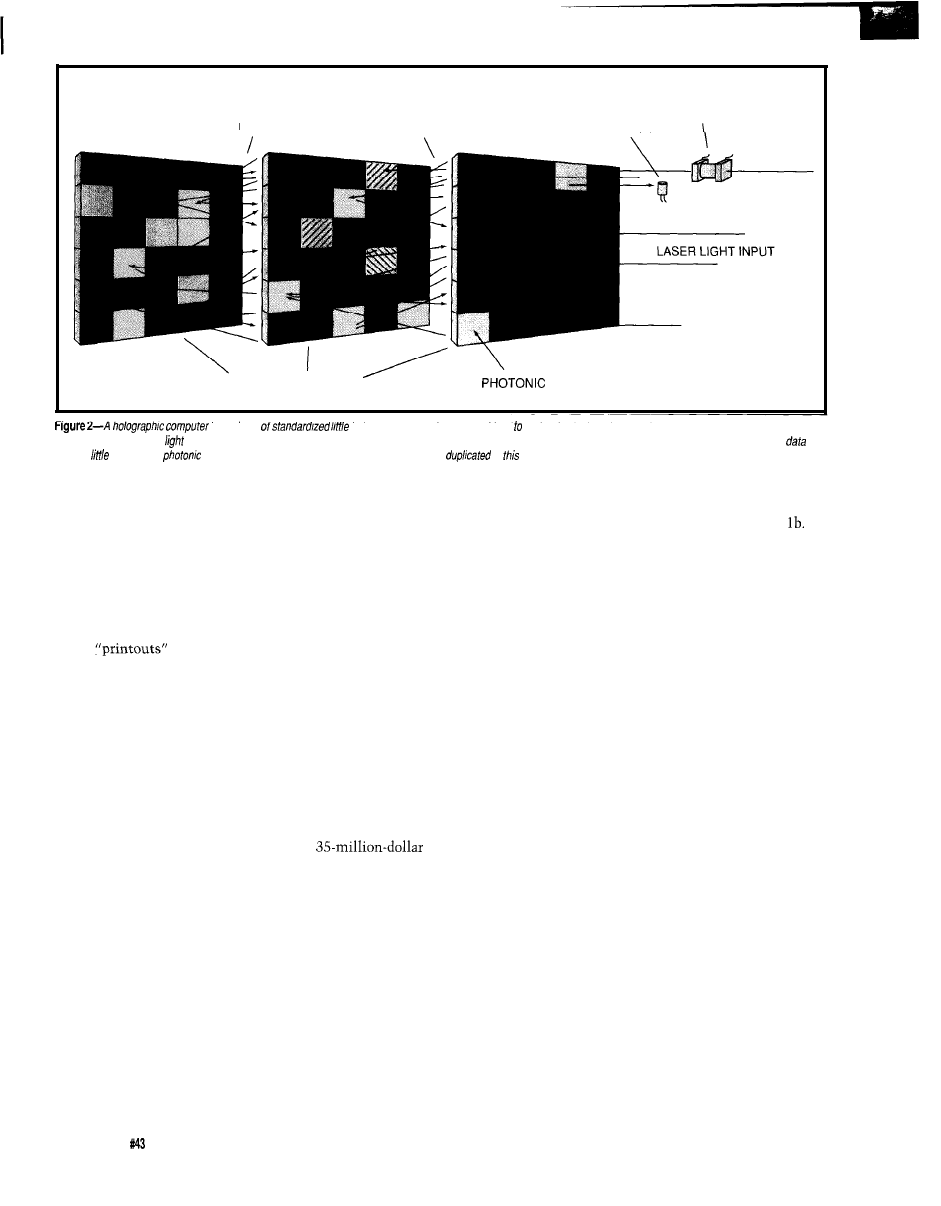
MAKING A HOLOGRAPHIC
COMPUTER
Figure 2 shows one possible
configuration for building a holo-
graphic supercomputer. It consists of a
large number of holograms laid out in
a checkerboard fashion, each square
being either a hologram, a fringe
component separator, or both.
Light from each square is directed
by its hologram to the squares in the
next plane. In this way, the logic
devices may be both constructed and
interconnected. Even data input and
output beams can be produced, and
laser “power” may be distributed to
each of the components as needed. By
arranging the various little square
holograms so as to cooperate together,
complete computer architectures may
be constructed.
Holograms also have the ability to
produce very complex images that can
be selected by individually directing,
not plain laser light at the hologram,
but by projecting an image onto the
succeeding hologram.
In Figure 2, the composite of little
holograms at each plane can be
considered as one big hologram with
many subhologram parts. If an image
is projected onto a composite holo-
gram, some of the little portions will
be lit and some will not. By specially
calculating each little hologram in
concert with the others, a different
image may be produced for each of a
number of input images. How would
that be useful?
If the input image consisted of a
number of beams that represented an
address bus, the combined output
through an array of mask openings can
be the completely decoded address.
Thus for each combination of input
beams projected onto the
combining hologram, only one mask
hole will be lit. Or if negative logic is
used (which has some advantages), all
would be lit except one. If the output
of such an address decoding array is
directed to an array of photonic
transistor flip-flops, the device is a
RAM. If the output is directed to a
viewing screen, the device is a com-
pletely photonic, high-speed video
display! By the way, the right configu-
ration can display in 3-D, too.
Are you ready to make some
synthetic holograms?
MAKING AND TESTING
SYNTHETIC HOLOGRAMS
Synthetic holograms are com-
puter-generated graphics. The pro-
grams are relatively simple, but they
take a very long time to run. They are
called ray tracing programs.
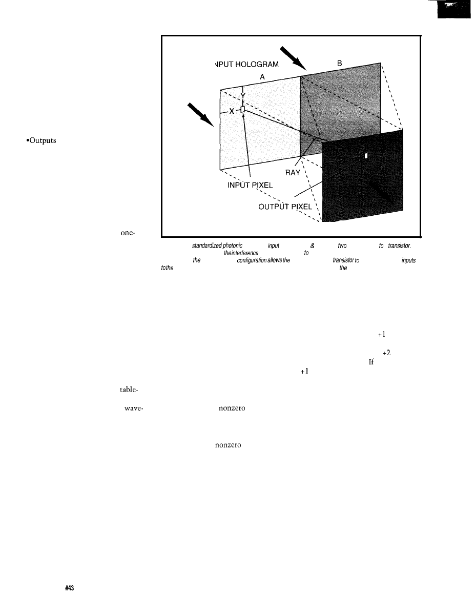
Figure 3 shows a standardized
configuration that includes two
standard input squares that cooperate
together to produce a standard output.
Each square may be a hologram, a
mask, or a combination. Light from
each input square is calculated using
the wave nature of light so as to
determine what pattern will be
projected onto the output square. By
doing two calculation sets, one for
each input square, three different
images can be produced on the same
output square. One for when one beam
is on by itself, and a second for when
the other beam is on by itself. By
summing these two calculated
outputs, the result from having both
beams on at the same time can be
produced.
By writing a set of basic inter-
changeable table-oriented algorithms,
several things become possible:
RELAY INTERFACE (16 channel) . . . . . . . . . . . . 89.9
channel
level) outputs are provided for
RELAY INTERFACE (2 relays, 10
REED RELAY CARD (8 relays, 10 VA) . . . . . . $49.9
RELAY
(10 amp SPOT, 277
A N A L O G
D I G I T A L
TO
CONVERTER* (16
CONVERTER’ (8
voltage, amperage, pressure. energy usage,
and a wide
of other types of analog
available (lengths to 4,000’).
for info on other
and 12 hit
(terminal block
sold separately).
TEMPERATURE INTERFACE’ (8
term. block temp. sensors
to 146’ F).
TA-8 DIGITAL INTERFACE’ (8 channel) . . . . . . . . . $99.9
on/off status of relays, switches,
equipment
devices, smoke detectors, and other devices.
TA-8D TOUCH TONE INTERFACE* . . . . . . . . . . . . . . . .
callers to select control functions from any hone
PORT SELECTOR (4 channels
an
port into
4 selectable
ports
O-485 (AS-232 to
your interface to control and
up to 512 relays, up to 576 digital inputs. up to
28 analog inputs up to 128 temperature inputs using
PS-4. EX-16, ST-32
expansion cards.
FULL TECHNICAL
over the
telephone by
staff Technical reference disk
including test software programming examples in
Basic, C and assembly ate provided with each order.
HIGH
for continuous 24
hour industrial
with 10 years of proven
performance in the energy management field.
CONNECTS TO RS-232, RS-422
with
IBM and compatibles, Mac and most computers. All
standard baud rates and protocols (50 to 19,200 baud:
Use
800 number to order FREE INFORMATION
PACKET. Technical information (614)
LINE (800) 842-7714
Visa-Mastercard-American Express-COD _
International Domestic FAX (614) 4844856
Use for information.
support orders.
ELECTRONIC ENERGY CONTROL,
INC.
380
South Fifth Street. Suite 604
Columbus,
432155438
The Computer Applications Journal
Issue
February 1994
1 9
*Holograms can be produced to form
specific output images.
*Images from each hologram and both
holograms together may be simu-
lated.
*Masks may be created to provide
predetermined outputs given all
input states.
*The operation of the full transistor
can be simulated for any set of
image inputs and for all states.
from one transistor can be
entered directly into a succeeding
transistor.
*Outputs from one transistor can be
routed to a succeeding device by
creating a hologram that simply
produces a plane output image,
which angles over to the output
position.
If viewed as a two-input,
output device, each of the four
possible states (including the moot
state where both beams are off) can be
simulated. If the two input squares are
holograms and the output square is a
mask, the operation of this synthetic
photonic transistor may be simulated.
Thus, your work may be tested
without even having a laser or any
other equipment other than a com-
puter.
By using standardized, inter-
changeable, pixel amplitude tables for
both input and output [albeit very
large ones), holograms, masks, and the
simulated operation of each can be
produced from a single set of
operating algorithms. The table
arrangement permits complex
fronts and images to be calculated
from a standardized data set. Thus, the
data output from one transistor can be
entered as a light configuration into
the next transistor. Complex products
can be built up one transistor at a
time.
Images calculated from pixel to
pixel produce the same mathematical
result regardless of which direction the
light is traveling. Data output tables
can be used as holograms from
predetermined images, images from
previous holograms, images from
images, and masks from image
combinations. Masks and holograms
can be superimposed upon input
STANDARD INPUT HOLOGRAM
STANDARD IF
-OUTPUT MASK
Figure 3-h a
transistor,
holograms A B provide
optical
inputs a
The
output mask separates
fringe
images so as produce signal amplification or boolean logic.
Standardizing hologram/mask
outputs from each
become fhe direct
next transistor. Thus, holograms and masks may be calculated easily and operation of each transistor may
be completely simulated and tested.
images so that each of the possible
input states may be simulated.
RAY TRACING PROGRAMS
Each standard square consists of
an array of pixels. Light which exits
each pixel initially heads toward all of
the pixels of the output square. The
line which connects an input pixel to
an output pixel is a ray. Thus, every
output pixel will have a ray coming
toward it from every one of the input
pixels that have a
input
amplitude.
By summing the instantaneous
amplitudes of light that arrives at each
pixel from every
input pixel,
the combined amount of light at that
pixel, for that instant, may be deter-
mined. By calculating every ray from
every input pixel to every output pixel,
the entire output image may be
produced.
The instantaneous amplitude from
each ray is proportional to the phase of
the light when it arrives at the output
pixel. If that instantaneous amplitude
is in phase with the input pixel
(assuming a positive input amplitude),
the output amplitude from that input
pixel is positive. If the ray produces an
instantaneous amplitude that is out of
phase with the input pixel, then its
instantaneous amplitude is negative.
If one ray produces a instanta-
neous intensity, and another also
produces a + 1, the result is (con-
structive interference). one produces
a and another a
-1,
the net result is
zero (destructive interference). The
calculated output for each pixel will be
the algebraic sum of all instantaneous
amplitudes from all input pixels.
What makes the phase change
from one pixel ray to the next?
Distance. The ray tracing program
calculates the 3-D distance from each
pixel in the input square to each pixel
in the output square. The distance is
converted to (a number + a fraction) of
wavelengths. The wavelength fraction
multiplied by the amplitude of the
input pixel equals the instantaneous
amplitude arriving at that output
pixel.
A mask or hologram graphic can
be superimposed onto a pixel table by
setting all pixels that match corre-
sponding black pixels in the graphic
equal to zero.
2 0
Issue
February 1994
The Computer Applications Journal
SYNTHETIC
TRANSISTOR DEVELOPMENT
PROCEDURE:
First, you need to select an input
table of pixel amplitudes either from a
previous run or one with all pixels
initialized to one (which represents a
plane wave of equal amplitude directly
from the laser). Next, calculate the
image output from the A input side of
the device. Now, produce a hologram
by setting each pixel in the graphic to
be either one or zero, to correspond
with the output pixels values from the
previous step. Set them by a predeter-
mined range for the type of device in
use (usually all negative values
produce zeroed pixels].
Next you need to superimpose the
graphic onto the original input table.
Then you have to recalculate the
image to determine if the desired
output has been achieved, adjust the
pixel setting parameters if needed,
and perform a loop at this point until
the desired output image is finally
created.
Then you need to produce a
similar hologram from the B side of
the device. Now you can produce a
combination image by summing the
two previous output tables. At this
point, it is a good idea to display and
check all states for the production of
the desired images. You may need to
iterate the process until the optimum
images are produced.
You will mask the output table
(by zeroing the desired pixels) to
produce the final transistor. Now you
have to test all three “on” states using
the same mask and the three previous
output tables to ensure proper opera-
tion. In most cases, the result should
be an image that is on or off (resulting
in a single output table) rather than a
complex set of images for each of the
input possibilities. Otherwise things
get real complex.
This photonic transistor is
complete. Go on to the next device by
adjusting the coordinates of the output
table to become an input table. Repeat
these steps until the product is done.
EXAMPLE FLOWCHART
PROGRAMS
I have included some examples to
explain the process in the simplest
possible way. They show how stan-
dardized tables can be used with
various algorithms for producing a
multitude of photonics products.
The actual table sizes, however,
are much too large for these exact
programs to function with practical
working holograms. So use these
programs more like flowcharts: as
teaching aids for understanding the
processes involved. Then, use your
own skill to produce working pro-
grams in whatever language you
wish.
Use the distance between the
input squares and the output square as
the minimum focal length times two,
so that the output square size will be
the same as the input squares. Note
that tables should be calculated with
at least
accuracy.
For a VGA screen, with 640
horizontal pixels, two 320x320 pixel
squares will display side by side. All
calculations will be done in
length units.
The flowchart-like routines shown
in Listing
1 give a sense
of how
photonic transistors based on syn-
thetic holograms are produced, but
this list is by no means exhaustive.
The problem is actual programs like
this run at a snail’s pace because the
run time is multiplied by the number
of input pixels that are not zero.
However, there is a great deal of
redundancy that one can capitalize on
in order to speed things up.
Standardized squares produce
standardized phase calculations. So,
working programs will probably use
table lookup procedures and
precalculated constants that are not in
the nested loop. Only the input
amplitude at each pixel changes, so
simple multiplication or addition need
be the only math function within the
loop.
Once certain types of transistors
are produced, it may be easier to adjust
the input light configuration to a
standard form so that preprocessed
data can be reused as much as possible.
In fact, the next logical step will be to
produce CAD programs that use
precalculated standardized units that
can be combined into various prod-
ucts.
Additionally, this process is well
suited to neural programming, Fourier
transforms, and other methods for
arriving at the iterated result much
faster. The point is that actual working
components can be synthesized within
a standardized configuration much
faster even though the computational
methods may differ.
Obviously, early programs will
proceed at turtle speed. Optimizing
and automating software will greatly
improve that speed. But as soon as the
first photonic processors and
are produced, production should take
off like a jackrabbit.
DISTRIBUTED DEVELOPMENT
If you had patented an important
invention, how would you develop it!
Find the most talented people?
Organize them into a productive
cooperating team? Locate the prime
production facilities? Determine what
is the most effective method for
beating the competition? Find the best
salespersons and the best advertising
method?
Where are the most talented
people? How do you find them for a
project like this, a process that has
never been done before, to produce
products that don’t even exist yet and
when the talent is spread all over the
earth? The answer lies in the very
process by which photonic computers
are made and the lessons of recent
history.
Synthetic holograms are essen-
tially made out of data. These days,
data can be transmitted virtually
anywhere. Such data is produced by
programs, written by programmers
who commonly work alone or in very
small groups. Therefore, there is no
reason whatsoever that they need to be
located at a central place. Everything
can be coordinated via telephone,
modem, and fax. Thus, the develop-
The Computer Applications Journal
attn: Subscriber Services
( 2 0 3 ) 8 7 2 - 2 2 0 4
l
22
Issue
February 1994
The Computer Applications Journal
l
***
ment of holographic computers lends
itself very well to a distributed
development process.
The personal computer revolution
was not the creation of one big
company, even though there were
some big players. It came about by the
hand of thousands of innovative
entrepreneurs-little people with big
ideas. Together, these people created a
revolution that has changed the world
and seen the lowly PC capture the vast
majority of the computing market. It
worked then, and will work now in the
transition from electrons to photons.
And what about advertising and
sales? There is no better advertising
than to offer products that outperform
the competition. The excitement that
creates is the best advertising.
How do we enlist the help of so
many talented people? We pay them!
Not by the hour, but by the product
sold. As new products are developed,
we will evaluate them in a coordinated
effort to find out who is able to
produce the best products for including
in our sales network (including
software products.) When accepted,
arrangements will be made for manu-
facturing, distribution and sales. Just
as with any other business, each one
does his part, and each one shares in
the fun and profit.
PROTECTING YOUR INVESTMENT
Programmable lightware, when
used with a laser, functions as active
patented photonic transistors. As such,
the computer-generated graphics you
develop may have important economic
value. Improper use or disclosure of
them may seriously hinder your ability
to secure intellectual property rights to
those images and the use thereof.
By law, no one has the right to
make, sell, or use a photonic transis-
tor, or the patented process that makes
them work, without license from the
Rocky Mountain Research Center.
Thus your output images can only be
used as actual functioning components
(even for private laser testing], if you
are a licensed part of our developing
and marketing network. That is a
protection for you from unlawful
competition to any product you work
with us to develop.
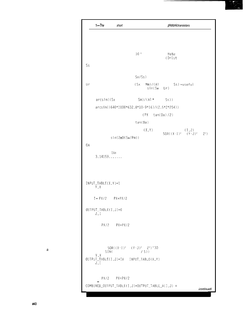
Listing
following
programs
are simple examples of how
are implemented.
Constants:
Al = antialialing factor = 2.5
Lp = lines/line-pair = 2
Mm = mm/meter = 1000
Sm = Synthetic wavelength multiplier = 16
w = wavelength = 632.8 *
meters for a
laser
PX = pixels on any 1 side of square = 319
pixel position)
Sx = pixels/full horizontal screen width = 640
= full horizontal screen width = 254 mm for a 10" wide screen
Useful formulae:
Pm = pixels/meter = (Mm *
= 2520 (rounded to nearest pixel)
S
W
= synthetic wavelength = w * Sm
= useful resolution =
*
* Lp *
Da = max deflection angle = arc
*
lines/m
Combining these:
Da =
* Mn * w *
Lp *
so:
Da =
= 0.29"
f = focal length in pixels =
*
Z = synthetic distance between input squares and output square in
pixels = 2 * f = PX *
= 63,222 pixels
D = distance from input pixel
to output pixel
=
+
+
Ph = Phase =
IA = Instantaneous amplitude = Ph * amplitude from input pixel
= Output amplitude at each pixel = algebraic sum of all
instantaneous amplitudes from all input pixels = IA1 + IA2 +
IA3 . . .
PI =
PROG 1: for plain laser input, initialize input pixels to
l...otherwise load an input table from a previous run.
FOR X = 0 TO PX
FOR Y = 0 TO PX
NEXT
PROG 2: to initialize an output table
FOR
TO
'because the output square is offset by
half a square
FOR J = 0 TO PX
NEXT
PROG 3: to calculate output table from input table A
FOR I =
TO
FOR J = 0 TO PX
IA = 0
FOR X = 0 TO PX
'to calculate from the B input square, use FOR X = PX TO 2 * PX
FOR Y = 0 TO PX
DISTANCE =
+
+
Pythagoras
IA = IA +
DISTANCE * 2x
'instantaneous amplitude
NEXT
*
NEXT
PROG 4: to combine the inputs from square A and square B to
determine the output result when both beams are on.
FOR I =
TO
FOR J 0 TO PX
2 4
Issue
February 1994
The Computer Applications Journal
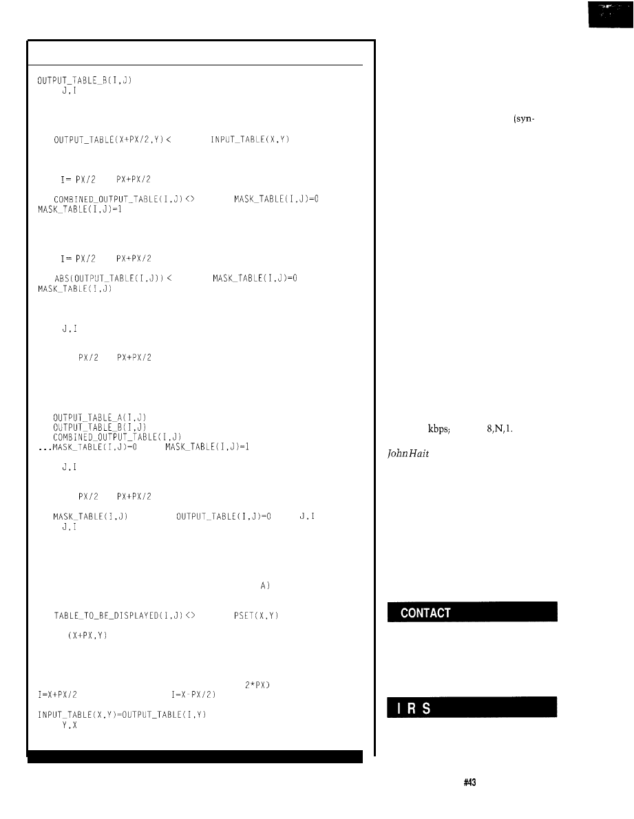
Listing l-continued
NEXT
PROG 5: to make an input hologram by making selected pixels black.
FOR X = 0 TO PX
FOR Y = 0 TO PX
IF
0 THEN
= 0
NEXT Y,X
PROG 6: to make an output DI mask by making selected pixels black.
FOR
TO
FOR J = 0 TO PX
IF
0 THEN
ELSE
NEXT J,I
PROG 7: to make an output CI mask by making selected pixels black.
V = a cut off value to be determined by needs of device.
FOR
TO
FOR J = 0 TO PX
IF
V THEN
ELSE
= 1 'if there's light there, let it through.
'notice that both positive and negative phases are there, and that
may, or may not be good, depending upon the design of the follow-
ing device.
NEXT
PROG 8: to make a mask with predetermined properties
FOR I =
TO
FOR J = 0 TO PX
'select the criteria for each pixel as to whether it should be
masked or not based on how that particular pixel behaves given the
three lighted input states of: beam A on, beam B on, and both
beams on.
IF
= (beam A on criteria)
IF
= (beam B on criteria)
IF
= (both input beams on criteria)
ELSE
'depending upon above
criteria
NEXT
PROG 9: to superimpose a mask onto an output table
FOR I =
TO
FOR J = 0 TO PX
IF
= 0 THEN
NEXT
NEXT
Note that the output through each mask must be checked in each of
the possible input states.
Masked should be designed to produce
only a single output image from the three input images.
PROG 10: to display the results (at position
FOR I = 0 TO PX
FOR J = 0 TO PX
IF
0 THEN
'turn on the
pixel
'PSET
for position B
NEXT J,I
PROG 11: to make the output of one transistor equal one of the
inputs of another transistor
FOR X = 0 TO PX
'(for input B use PX to
'(for input B use
FOR Y = 0 TO PX
NEXT
The actual patented process
involves the use of any means for
producing interference fringes, and
then using any means for separating
those fringes into their component
parts. That coverage is very broad.
However, computer graphics
thetic holograms and masks) made and
tested by simulation, as described
above, are not covered by patent law
because they are just simulations.
By becoming a part of our net-
work, your product will be both
protected and defended. What’s more,
those who are a part of the coordinated
network will have access to the latest
information so that they will always
be on the leading edge, not duplicating
the work of others.
So whether you prefer to write the
synthetic-hologram-producing soft-
ware, or produce holograms using this
method, you may wish to have your
work evaluated as a potential product
for sale through our network. Neat
idea, huh? You can find out more by
accessing our new Photonic Transistor
BBS at (406) 273-4692. Call in often, as
new material will be continuously
added as photonic development
proceeds. Our BBS supports data rates
up to 14.4
and uses
q
is an electronics engineer
with over 35 years of experience in
basic circuit design and troubleshoot-
ing electronic and data processing
systems, He is best known by his
books and articles on practical
applications of thermodynamics and
electrochemistry. He is the inventor of
the photonic transistor, which is only
one of 85 inventions that span the
wide spectrum of practical physics.
Rocky Mountain Research Center
P.O. Box 4694
Missoula, MT 59806
(free catalog and network
information available)
401
Very Useful
402 Moderately Useful
403 Not Useful
The Computer Applications Journal
Issue
February 1994
2 5
In the Eye
of the
Beholder
Displaying
Messages
with the
II
J. Greaney
walk into the
room and, tucked
spy a vertical column of
flickering just slightly. “What’s
that thing supposed to do!” you ask
yourself. Shrugging, you redirect your
gaze to more interesting matters. As
you turn away, you think you see
something from the corner of your eye,
but then it’s gone. You look back at
the
to find them still flickering
ever so innocently. Turning away, you
again catch a glimpse of a picture.
You’ve just discovered the
Bill Bell’s United States patent
calls his light stick a “Momentary
Visual Image Apparatus.” It is a device
that creates an optical illusion that is
formed by multiplexing the multiple
columns of an image onto a single
column of
Everyone has seen
examples of
x n-pixel arrays used to
create two-dimensional images. PC
graphics adapters support 1024 x 768,
800 x 600,640 x 480 to name a few.
Old dot matrix printers supported 5 x 7
characters. From the instant replay
screen in the football stadium to the
graphics display on my HP
they
all share something in common. The
images all consist of static arrays of
columns of picture elements. The
specific spatial displacement in x and y
required by each individual pixel is
provided by the physical display.
What a light stick does differently
is to display all m columns of the
picture on a single column of pixels.
Construction of the image
depends on the human eye’s persis-
tence of the retina and on its natural,
rapid movements from one point of
fixation to another.
The persistence of the retina gives
you after-images from flash bulbs and
allows you to draw line images with
Fourth of July sparklers. The rapid eye
movements are involuntary and you
are probably unaware of the fact that
you are doing it. Normal visual
activity consists of fixating on a point
of interest, capturing the visual
information, and then rapidly moving
to the next point of interest. During
the transition from one point to the
next, normally no visual information
is gathered. Everything would appear a
blur and is ignored. It is during this
time that the light stick works.
If you look directly at the column
of
you will perceive it as a
flickering or shimmering stick of light.
As the individual pixels are rapidly
turned on and off it appears that they
are either continuously on, or off, or
being slightly modulated in intensity.
If instead you ignore the stick and let
your eyes wander around the room, the
horizontal motion of your eye will
spread the columns across your retina,
thus building up an image that exists
as long as your persistence of the
retina holds it.
My light stick was inspired by one
of Bill Bell’s light sticks that was on
display at the Exploratorium in San
Francisco back in 1986. The
Exploratorium is a nonprofit science
museum that everyone should visit at
least once, and Bill Bell’s light stick
optical displays are certainly among
the most striking and interesting
pieces of modern art.
Photo
image produced
by the
is
painted on your retina as you
look past
device. While it’s easy to see the image here, gone
in an instant when you look at the
display.
26
Issue
February 1994
The Computer Applications Journal
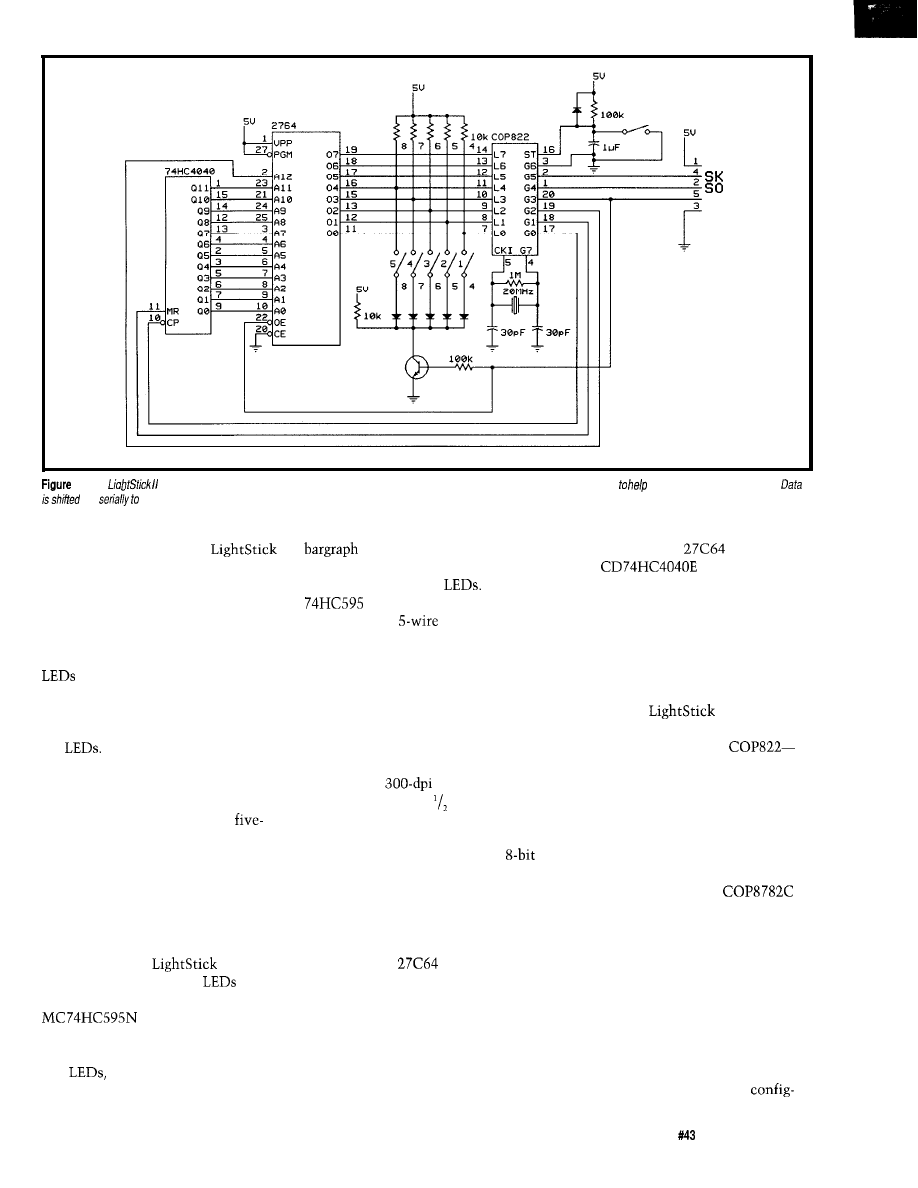
STRB
la--The
controller couldn’t be simpler, using a COP for the brains, an EPROM to ho/d image data, and a counter
with the EPROM addressing.
out
the stick itself.
THE LIGHTSTICK II
The basic operation of
II is very straightforward. The picture
data is stored in an EPROM (see Figure
1). A microprocessor retrieves the data,
one byte at a time, and shifts it into a
string of 20 serial-to-parallel convert-
ers that are located adjacent to the
in the stick. This continues until
an entire column-20 bytes-is shifted
in. It waits for a specified period of
time, then strobes the data out onto
the
Then it goes back and gets
another column. This cycle continues
and repeats after 204 columns.
The hardware consists of two
subassemblies connected via a
wire cable: the LED display and the
microprocessor-based controller. The
cable provides DATA, CLOCK, and
STROBE logic signals for the stick as
well as power and ground.
THE STICK
The stick for
II consists
of a single column of 160
with
National Semiconductor
serial-to-parallel
converters to drive them. While Figure
lb shows just ten sets of converters
and
the second group of ten is
wired exactly the same.
I chose HP HDSP4830 lo-segment
LED modules because of the
ease of lining up 10 LED segments as
opposed to individual
The
allowed me to have a serial
data bus and a
cable from the
control board to the stick display
board. Five-conductor DIN connectors
made the whole system easy to break
down and reassemble.
I chose the height of 160 pixels
based on the original bitmap that I
wanted to display. I obtained a bitmap
of the AT&T company logo that was
intended for
laser printers. The
logo is 150 pixels (or inch) high and
336 pixels wide. The LED arrays are
grouped as 10 LED segments, and the
microprocessor likes to work in
bytes, so 160 is a convenient height.
The logo is 42 bytes (336 pixels) wide,
so I divided it into two pictures and
padded each out to 204 columns so
that each would occupy approximately
one half of the
EPROM.
Splitting the logo into two parts also
keeps the image simple and easy to
view. More on this later.
THE CONTROLLER
The controller subassembly
consists of a National Semiconductor
COP822 microprocessor emulator, a
five-key keypad, a
EPROM, an
RCA
ripple counter to
help out with addressing the EPROM,
and a reset button.
I chose the COP822 based on its
projected cost in large volumes.
Because of its low cost, we were
planning to use the COP822 to replace
some discrete logic in one of our
designs. The
II project
provided an excellent opportunity to
learn how to program the
and microprocessors in general-since
I am primarily an RF engineer.
The actual processor I used was an
EEPROM COP8722, which was a
limited-production version of the
COP822 emulators used for early
development. National Semiconductor
has since come out with
OTP and UV EPROM parts that would
provide a more cost-effective solution
for development and limited produc-
tion use.
The 20-pin COP822 has two I/O
ports available on it: the L port and the
G port. The L port is a full 8 bits wide
while the G port is only 7 bits wide.
The chip also has a timer function and
a serial port. To use the serial port, the
upper 3 bits of the G port are
The Computer Applications Journal
Issue
February 1994
2 7
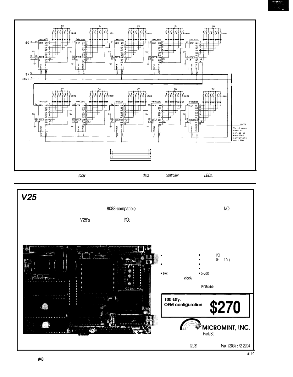
T O C O N T R O L
C A B L E
T O S T I C K
Figure 1 b--Twenty
serial-to-pm//e/ converters
half are shown here) are used to receive
sent by the
for display on the
POWER COMES TO EMBEDDED CONTROL!
Micromint’s RTCV25 is the perfect marriage of an
processor, programming convenience, and control
Forget
the need for cross-assemblers and cross-compilers; your favorite high-level language for the PC and a “locate” facility are all you
need. The RTCV25 enhances the
power with parallel
A/D conversion; RS-232 and RS-485 serial ports; up to 384K of
RAM and EPROM; a battery-backed clock/calendar; 128 byte EEPROM, ROM monitor, and the RTC stacking bus. Ease of code
development combined with its small size and low power consumption make the RTCV25 ideal for all embedded control applica-
tions. And of course the RTCV25 is compatible with Micromint’s full line of RTC peripheral boards and products.
Features:
8 MHz CMOS NEC
V25 processor
Up to 384K of RAM
and EPROM
serial ports
l
Battery-backed
calendar
l
128 byte EEPROM
40 parallel lines
d-channel, (or
bit ADC
RTC stacking bus
Small 3.5” x 5” size
only operation
(150mA max.)
l
Full featured ROM monitor
l
operating system
4
l
Vernon,CT 06066
call l-800-635-3355
871-6170
l
28
Issue
February 1994
The Computer Applications Journal
ured as Serial Clock, Serial Output,
and Serial Input. Since I am not
interested in receiving serial data, I
grounded
the Serial Input. The
lower 4 bits of the G port are used to
control the addressing of the EPROM
(with help from the
and to
control the strobe signal to the
The strobe signal is also
used to activate the
keypad. I
use the L port for data input from both
the
data from the EPROM
and the
keypad.
The image size of 204 x 160 (4080
bytes] allows two uncompressed
images in the
ROM. Keep in
mind that the final image exists only
in the persistence of the viewer’s
retina, so you want to keep it as
narrow and as simple as possible.
The keypad is used to control the
display of the image. I set a default
time delay between column strobes
that is a compromise between how
narrow the image will appear and how
much the leading edge of the image
fades by the time the trailing edge is
displayed. You may adjust this time
delay using the “faster” and “slower”
keys on the keypad. The three other
keys allow you to invert the image,
choose between the two images in the
ROM, and toggle between Normal and
Slow mode. In Slow mode the control-
ler clicks off a column every 100 ms
(adjustable) for diagnostic purposes.
Also, in Slow mode, pressing both
“faster” and “slower” together puts
you into a Halt mode where you can
single step through the ROM one
column at time.
THE POWER SUPPLY
The HP HDSP4830
are rated
at a maximum DC forward current of
30
At 20
the typical forward
voltage is
1.6
V. I chose to run them at
the maximum DC current to get as
much light out as possible while still
allowing for the Halt mode where the
may be illuminated for an
indeterminate period of time-a 100%
duty cycle. I make the assumption that
the forward voltage will approach 2.0
V at 30
This leads to a
limiting resistor of
Fortunately,
each current-limiting resistor only
dissipates a maximum 116
so I
chose a resistor array package, making
the assembly more elegant. The
are conservatively rated;
I
plan to use
them in pulsed mode most of the time,
and, most importantly, I socketed
them.
Assuming a worst-case LED
current of 34
160
on would
draw 5.44 A! This is not counting the
shift registers and control circuits. I
chose a supply that sources 6 A at 5 V.
SOFTWARE
The COP800 cross-assembler
listing for the most recent version of
microprocessor code is available on the
Circuit Cellar BBS. The comments in
the beginning include the values
stored in memory locations unique to
the COP8722 EEPROM emulator.
Address 804 prevents modifying the
ROM section once programmed.
Address 805 contains configuration
information relating to the
selectable oscillator options: divide by
10 or 20 and either RC, crystal, or
EXPRESS CIRCUITS
MANUFACTURERS OF PROTOTYPE PRINTED CIRCUITS FROM YOUR CAD DESIGNS
TURN AROUND TIMES AVAILABLE FROM 24 HRS
2 WEEKS
Special Support For:
l
TANGO.PCB
l
FULL TIME MODEM
l
TANGO SERIES II
l
GERBER PHOTO PLOTTING
l
TANGO PLUS
l
PROTEL AUTOTRAX
l
PROTEL EASYTRAX
l
l
l
II
l
EE DESIGNER I
l
EE DESIGNER III
l
ALL GERBER FORMATS
WE CAN NOW WORK FROM
YOUR EXISTING ARTWORK BY
SCANNING. CALL FOR
DETAILS!
Circuits
Quotes:
l-800-426-5396
Phone: (919) 667-2100
Fax: (919) 667-0487
1150 Foster Street
l
PO. Box 58
Industrial Park Road
Wilkesboro, NC 28697
The Computer Applications Journal
Issue
February 1994
2 9
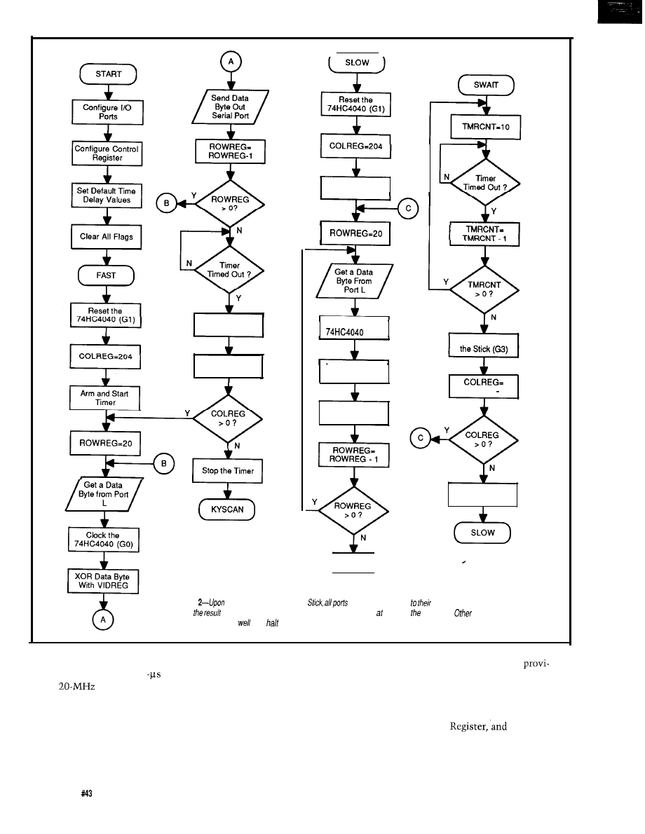
Configure I/O
Ports
Strobe Column on
the Stick (G3)
COLREG..
COLREG-1
Stop the Timer
KYSCAN
Arm and Start
Timer
Clock the
(GO)
XOR Data Byte
with VIDREG
Send Data Byte
Out Serial Port
Stop the Timer
KYSCAN
Strobe Column on
COLREG 1
Figure
initialization of the Light
and registers are set
default
values. The actual image you
see is
of data being sent out, very quickly, one column a fime in main loop.
loops include key and
keypad scanning, as
as a
mode.
external clock. I chose crystal and
divide by 20 to give me a 1
clock
with a
crystal (the fastest
instruction clock possible). Locations
800 through 803 hex are available for
comments. I used them for the date
and iteration number of the code.
The code may be logically broken
up into five routines: an initialization
routine where default values are set;
software interrupt. I have no
two display loops, one fast and one
sions for using software interrupts, so
slow; a keypad servicing routine; and
if one occurs, it is probably a good idea
an auxiliary halt mode loop. See Figure
to reinitialize everything. This routine
2 for a flowchart of the whole system.
configures ports L and G, configures
the Control
sets the
INITIALIZATION
following conditions: do not invert the
This routine is run upon power
outgoing data, there is no current
up, hard reset, or in the event of a
keypress, the column time delay for
30
Issue
February 1994
The Computer Applications Journal
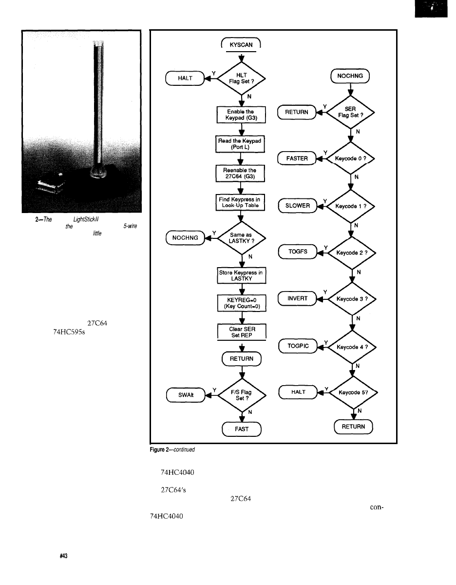
Photo
complete
consists
of a
controller board and display connected by a
cable. The display stick stands a
under two feef
tall.
Slow mode is 100 ms, the column time
delay for Fast mode is 466 us, and the
serviced flag is set.
MAIN LOOP
The main loop’s primary responsi-
bility is to extract one column of
picture data from the
and shift
it into the
as quickly as
possible so as to allow for maximum
variability in column timing. After
shifting in an entire column, it waits
for the column timer to expire before
strobing the new column onto the
stick and starting over again.
Optimizing the routine for speed
means optimizing for the minimum
number of clock cycles used by the
instructions within the Fast loop. For
this reason, keypad scans are made
outside the loop, in between picture
displays. Register Indirect instructions
only take one clock cycle as opposed
to three clock cycles for Memory
Direct instructions. If two or more
instructions are going to operate on
the same location in memory (Port G,
for instance), it makes sense to spend
the three clock cycles it takes to load
the address of the memory location
into register B, thereby minimizing the
overall total number of clock cycles.
RETURN
FAST
NOCHNG
I/O savings are realized by using
SECONDARY LOOP
the
ripple counter to
The secondary loop performs
sequentially step through one half of
basically the same as the main loop
the
address space. Since both
except it does a key scan after every
the ripple counter and the
take
column instead of after each complete
a little while to stabilize, I clock the
picture since I am not as time
immediately after getting a
strained.
data byte to maximize the time
This loop is really slow, so it
available for this settling.
counts up
10
timer periods instead of a
32
Issue
February 1994
The Computer Applications Journal
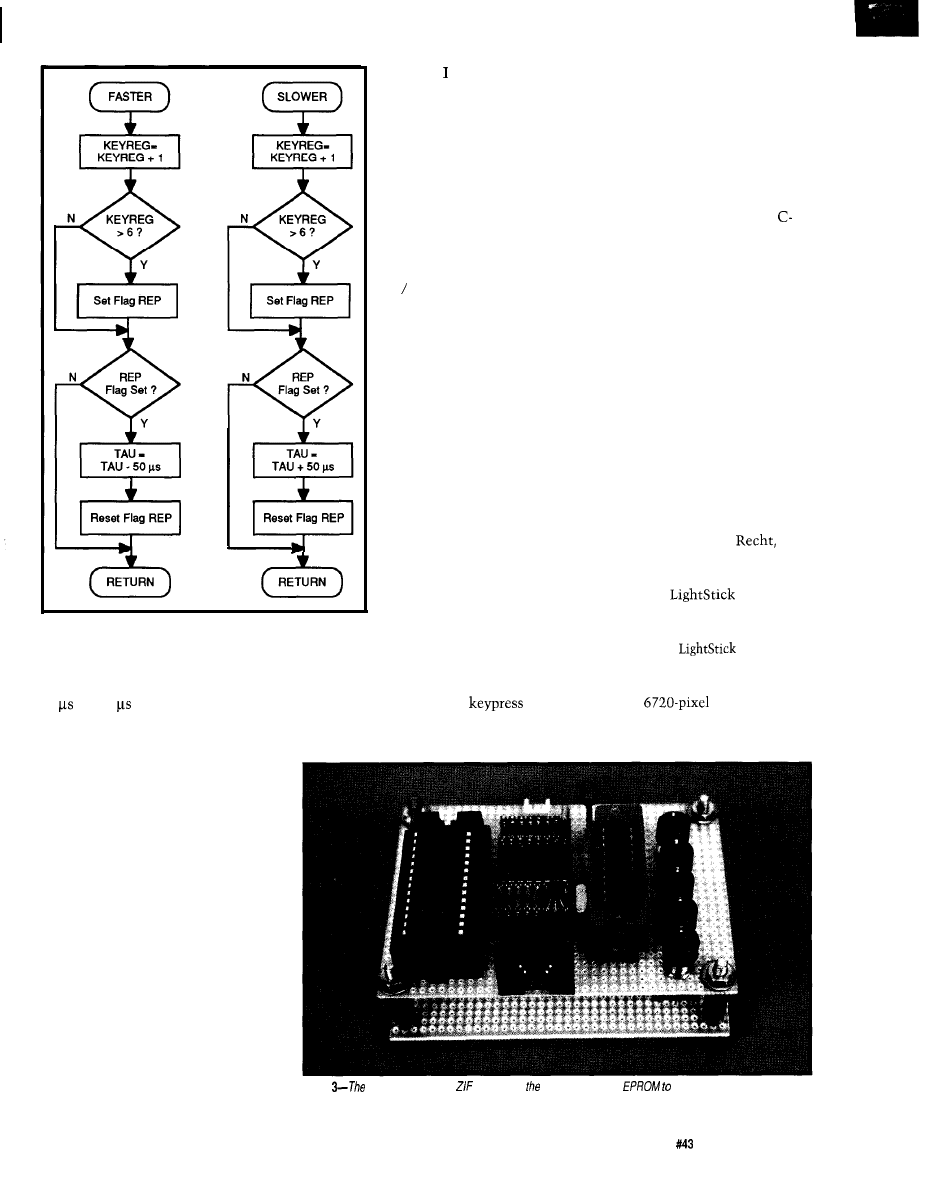
RETURN
RETURN
Figure
2-continued
indicating
should repeat
the modification to the
time delay. SE R keeps
track of whether the key
request has been serviced.
H LT indicates
Halt
mode,
used for branching back
into the Halt routine. PI C
indicates which picture is
current. I NV keeps track
of whether or not to
invert the outgoing data.
F S indicates either Fast
or Slow mode, used for
branching at the end of
the key scan routine. S LW
is a Slower request, so I
have to increase the time
delay. FST is a Faster
request, so
I
have to
decrease the time delay.
HALT MODE
Halt mode may
almost be considered a
limited functionality
subroutine of the keypad
routine. When in Halt,
the keypad is continu-
ously examined for one of
only two valid
keypresses: Step or
single timer period for the main loop.
This also changes the effective timer
increment/decrement time slice from
50 to 500 and allows me to use
the same time delay adjustment
routine for both the Fast and Slow
time delays.
Continue. Just as the regular Keypad
routine either jumps back to Fast or
Slow depending on where you came
from, when you get a Step
you go back to the parent process and
execute only one column for Slow or
KEYPADSCAN
The primary responsibility of the
Keypad Scan routine is to get updated
configuration information in between
pictures in the Main Loop or in
between columns in the Secondary
Loop. The types of things you want to
adjust are how quickly you walk
through the columns, which picture
you want to display, whether or not to
invert the picture (“on” for “off” and
“off” for “on”), and which primary
mode you want the processor to
operate in: Fast, Slow, or Halt.
To help me keep track of where I
am in the Keypad Scan, I defined eight
flags. RE P helps me keep track of a key
that is continuously held down
one picture for Fast. When you go for
another key scan you are placed back
in Halt. The only ways out of Halt are
Continue and Reset.
TRANSLATION UTILITIES
Since the column-at-a-time, 204 x
160, two-color picture format is not an
accepted standard yet, a couple of
code programs were written to trans-
late data from the existing, more
common standards into STK-light
stick-format. Both of these programs
are available on the Circuit Cellar BBS.
The company logo image data was
given to me in an unformatted 336
wide by 150 high two-color binary file
that was organized as a sequence of
rows starting from the upper left
corner of the picture. That’s 6300
bytes of input picture data. I had to
convert the data into a stream of ASCII
represented hex bytes that were
grouped one column at a time starting
from the upper left hand corner of the
picture.
A friend at work, Tom
wrote the original translation program
that took the raw binary input file and
rearranged it for
I (yes, there
was a version before this one). I
modified this program to create
X LATE 2 . C, the
II transla-
tion program.
Since the stick is 160 rows high, a
336 x 160 or
buffer is
created and initialized. The binary
input file is then read into this 6720
Photo
controller
board has
sockets for the processor and
make if easier to change the
control code and the image displayed.
The Computer Applications Journal
Issue
February 1994
3 3
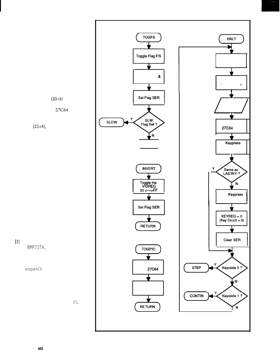
array of bytes where each byte repre-
sents a single pixel of the picture. The
picture is stored in the original data
file such that the most-significant bit
of the first byte is the upper left corner
of the picture, and the buffer is
arranged such that the first byte is the
upper left corner so that the index
loops used to write the data can start
at zero and increase monotonically to
read from left to right and top to
bottom.
The company logo is not exactly
symmetrical, so the first half is only
160 columns wide
with real
data, and the file is padded with 896
null bytes to pad the
EPROM to
4096 bytes for the first half of the logo.
The second half has 176 columns of
real data
so it only needs 576
null bytes of padding to fill the second
4096 bytes of the EPROM.
The output file is written as ASCII
represented hex bytes. Another friend
at work, Bruce Haggerman, wrote a C
utility that takes such a hex file and
adds the appropriate addresses and
checksums to create an Intel hex
format file ready to download to the
PROM programmer.
Eventually, the company logo gets
kind of old. To give myself some
practice coding C, I wrote a program
that takes uncompressed, B&W,
windows BMP image files, pads or
truncates the image to the 204 by 160
light stick size, and generates an ASCII
represented hex output file. I found the
windows BMP file and image headers
explained in “Graphics File Formats.”
In
C, I tried to write
code that I could easily modify for
other programs. To that end there is a
general-purpose, configurable
f i 1
routine that tries to get
all the input and output file informa-
tion from the command line argu-
ments. If this fails; it will prompt the
user for the information.
The routine of interest from the
light stick perspective is read This
routine defines two structures to
extract size and configuration informa-
tion from the file and image headers.
Using information in the headers, I
check for valid BMP file type, check
for the two-color requirement, and get
Exchange
Working TAU
Memory TAU
Set Flag SER
RETURN
INVERT
Toggle the
00
Toggle G2 Al 2
of the
Set Flag SER
Set Flag HLT
Enable the
Keypad (G3)
Read the
Keypad
(Port L)
Reenable the
(G3)
Find
in
HALT Look-Up
Table
Same as
LASTKY ?
N
Store
in LASTKY
Clear SER
Figure
2-continued
34
Issue
February 1994
The Computer Applications Journal
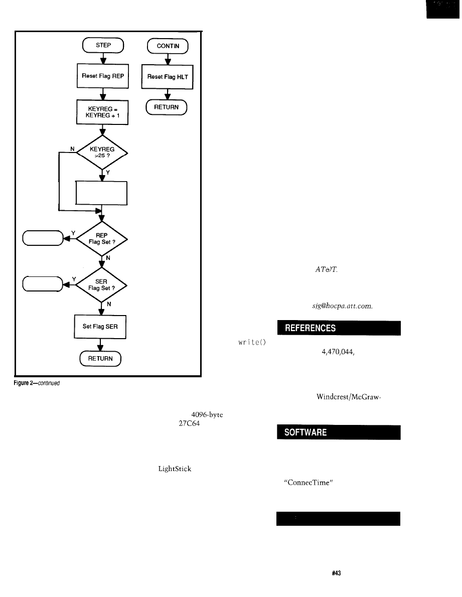
Set Flag REP
RETURN
HALT
loop sizes from the image size data
fields.
The BMP image format requires
the data stored in the BMP file to fall
on 4-byte boundaries for image width.
If the actual image size does not fall
onto a 4-byte boundary, the image data
is padded with garbage out to the next
4-byte boundary. It is the responsibil-
ity of the display program to get the
actual image size from the image
header and to crop this garbage data
out of the displayed image.
I have a 204 wide by 160 high
buffer that is initialized to 00. As I
read the BMP into the buffer, a row at
a time, I check to see if I exceed the
buffer width. If so, I keep reading bytes
in and discard
them. I store the
data into the
buffer one pixel at
a time, from left
to right. If the
image is less than
204 pixels wide
and not an integer
number of 4-byte
blocks wide, I
stop transferring
pixels at the last
data bit of
significance. Since
the buffer is
initially set to all
00, the image is
effectively padded
out to 204 pixels
wide. The other
interesting thing
about BMP files is
that they are
arranged with the
lower left corner
of the picture
first. This means
the upper and
right edge of the
picture will be
clipped if it is
larger than 204 by
160.
The
routine is very
similar to that of
the XLATE2.C
program. It also
pads 16 bytes to
make up the difference between the
4080 bytes in one 204 x 160 light stick
image and the
capacity of
half of the
EPROM. This
program takes two BMP files as input
and generates one STK file as output.
CONCLUSION
II provides a fairly
flexible architecture for examining the
optical effect described by Bell in his
patent. This allows you to play with
both the type of picture and the
display parameters of the picture. Keep
in mind that the COP assembly code
and the C code were written by an RF
engineer, so if you believe there is a
more efficient or elegant way of
writing the code, you are probably
right. If you do rewrite any of the code
to be more flexible, efficient, or
elegant, I would be interested in
hearing about your efforts.
The type of information that may
be successfully displayed is somewhat
limited by the humans that are going
to observe it. When I first wrote the
B M P 2 ST K . C translation code, I fever-
ishly converted a couple of B&W
digitized pictures to the stick format.
I
then spent half an hour getting a sore
neck trying to view them. The best
images are simple geometric shapes,
words with few letters, and stick
figures. Even the Circuit Cellar INK
logo used in the photo for this article
presents a challenging image to view
in its entirety. So, don’t worry if you
are not the most elaborate Paintbrush
artist in the world; the people who
would be required to view your
creation don’t exist yet anyway.
q
Shaun Greaney is an RF Design
Engineer at
He holds a BSEE
from Rensselaer Polytechnic Institute
and an MSEE from the University of
California, Berkeley. He may be
reached at
1. Bell, Bill, United States Patent
Number
“Momen-
tary Visual Image Apparatus,”
1984.
2. Kay, David C. and John R.
Levine, “Graphics File For-
mats,”
Hill, 1992, ISBN 0-8306-3059-
7.
Software for this article is avail-
able from the Circuit Cellar BBS
and on Software On Disk for this
issue. Please see the end of
in this issue for
downloading and ordering
information.
404
Very Useful
405 Moderately Useful
406 Not Useful
The Computer Applications Journal
Issue
February 1994
3 5
free
Design
Do-While Jones
these days to find a
anything you build will have some
digital logic in it. Unless that logic is
so simple that it can be done with a
few gates and a flip-flop or two, the
logic will naturally be done by a
microprocessor. The microprocessor
frequently controls peripheral devices
that are attached to it with interrupts,
and that is often a mistake.
Using interrupts for peripheral
control is so universally accepted that
it is seldom questioned. Certainly
there are times when using interrupts
makes good sense, but there are other
times when the use of interrupts can
make the design more difficult.
Knowing how to recognize situations
when it is wise to use interrupts or to
avoid them like the plague will lead to
an interrupt-free design that may be
cheaper, simpler, and more reliable.
A SHORT HISTORY OF
INTERRUPTS
If you know why interrupts were
invented, your understanding of what
kind of problems they solve will help
you decide if they are beneficial to
your design or not. So, let’s return to
the early 1960s and reminisce about
what it was like to use an IBM 1620
computer.
In those days, clock speeds were in
the tens of kilohertz (not tens of
megahertz). The bits on the data bus
changed so slowly that the IBM 1620
had a speaker attached to one of the
data lines and you could hear the bits
flip. After a while you could tell
whether your program was operating
correctly by the sound coming from
the speaker.
The 1620 had only one terminal,
one card reader, and one card punch. It
could only run one program at a time.
But there were many people who
wanted to use the computer and they
didn’t want to wait in line to submit
their decks of punched cards. So,
someone got the bright idea to connect
multiple terminals to a single com-
puter and make it serve them all
simultaneously (or at least, apparently
simultaneously).
At first, I’m sure someone must
have tried to poll the terminal to see if
a user had pressed a key. They possibly
tried to poll each terminal ten times a
second to see if the user had pressed a
key, but in those days it probably took
about 20 clock cycles to poll a
terminal’s status register. Suppose you
poll 15 terminals 10 times per second
on a computer with a
clock.
Twenty cycles at 10
is 2 millisec-
onds. Multiply that by 15 terminals 10
times per second, and you will see that
300 milliseconds of each second would
be used just to see if any key has been
pressed. Nearly a third of the CPU
time was wasted just checking to see if
any key had been pressed (and discov-
ering that one had not been pressed).
Computer time was too valuable to be
wasted that way.
About the same time user termi-
nals were invented, punched cards
were being replaced by magnetic files
on drums or disks. Bits were read from
a sector as the magnetic media passed
under the read head. The bits were
stored in a buffer and had to be written
to the proper memory locations before
the next sector could be read. If the
buffer wasn’t flushed in time, the
computer had to wait for a complete
revolution before the next sector could
be read. The computer couldn’t do
anything else while the buffer was
being filled because it had to be ready
to empty the buffer as soon as the
buffer was filled. This also wasted
valuable computer time.
Interrupts were invented to solve
these two problems. They eliminated
the need for the computer to waste
time checking all the terminal ports
because the terminals could interrupt
36
Issue
February 1994
The Computer Applications Journal
whatever the processor was doing to
get attention. The computer could
process data while sectors were being
read into the disk (or drum) buffer
because the buffer would interrupt the
computer when it was full and needed
emptying. People learned that if they
wanted fast response time and low
overhead, interrupts should be used.
Over the years, it became standard
practice to use interrupts to interface
peripherals to computers. In a
purpose, multiuser computer, that is
still the wisest thing to do. Interrupts
(and the associated file control blocks]
make it easy to configure operating
systems to support a wide range of
peripheral devices. They maximize
throughput because the computer can
do a background job when the periph-
erals don’t require attention. The
modern operating systems we have
today could not be built without
interrupts. Interrupts are an essential
part of general-purpose computing.
DIFFERENT NEEDS
Most of the circuits designed are
for special-purpose applications. The
microprocessor put in a microwave
oven, VCR, or television set does not
need a multiuser operating system. It
doesn’t need a system administrator to
add new users or install new peripher-
als. An embedded system specializes
in doing one job and it usually needs to
do it virtually instantaneously. It
doesn’t need the versatility interrupts
provide and can’t afford to spend the
extra time needed to process them.
Some designers don’t seem to
recognize the difference between a
general-purpose computer and a
dedicated controller. For example, it is
common to see an A/D converter
attached to an interrupt handler in a
dedicated controller design. This is
never a smart thing to do. If you ask
the designer why he did it that way he
will probably say, “I used an interrupt
because I needed fast response time.”
That’s like saying, “I made it out of
solid gold because I needed it to be
cheap.”
An A/D converter satisfies neither
of the two criteria for correct use of an
interrupt. Interrupts should be used
when
(1) you
can’t predict when data
will be available and data must be
taken from the peripheral promptly or
it will be lost. Dedicated controllers
always know when data from an A/D
converter will be available. It comes at
a periodic rate synchronized to a clock.
It should be no surprise that data is
available. Furthermore, it is the
program that must have the data
promptly, not the peripheral that must
have the data taken from it promptly.
Consider what happens in a
typical dedicated controller if it polls
to collect data from an A/D converter.
At regular intervals it fetches the data
from the last A/D conversion, starts
the next conversion, and processes the
•J Interrupts should
only be used in those
situations that are so
important, the com-
puter must stop what-
ever it is doing to re-
spond to them.
data from the last conversion. When
all the processing is finished, it sits in
a tight loop “wasting” machine time
polling a timer to see if it is time to
begin the next processing cycle. [This
time isn’t really wasted because there
is nothing else the controller could be
doing.)
If you do the same thing using an
interrupt, the processing takes a little
longer. At regular intervals the
controller fetches data which was
stored in memory from the last A/D
conversion, starts the next conversion,
and processes the data from the last
conversion. At some time during this
processing sequence the computer is
interrupted by the completion of the
A/D conversion. The computer stores
all the registers on the stack, fetches
the data from the A/D converter, and
stores it in the same memory location
that it just recently fetched data from.
Then the interrupt-service routine
restores all the registers and returns to
the interrupted program. It finishes
processing and spends a little less time
waiting for the next cycle to start
because it had to spend some time
saving and restoring registers. If there
was just barely enough time to do the
essential processing, the accidental
overhead of the interrupt servicing
may cause the program to miss its
deadline.
The situation is even worse if the
dedicated controller uses a processor
with a typical operating system. At
regular intervals it fetches data which
was stored in memory from the last
A/D conversion, starts the next
conversion, and processes the data
from the last conversion. At some
time during this processing sequence it
is interrupted by the completion of the
A/D conversion. The task context is
saved and the interrupt-service routine
fetches data from the ADC and stores
it in memory. Then the operating
system spends more time deciding
which tasks are eligible to run and
picks one of them to run next. If you’re
lucky, it will decide to resume the task
that was interrupted. The context
switching time may exceed the
essential processing time and there is a
very good chance the program will not
be able to meet its deadlines.
It is always faster to poll a
peripheral’s status port to make sure it
is ready and then transfer data to (or
from] the peripheral’s data port than it
is to respond to an interrupt generated
by the peripheral’s status port.
Furthermore, interrupts just annoy
the processor by telling it exactly
when new data is available. In the
example above, the processor doesn’t
care when the A/D converter finishes
its conversion. It only cares that the
conversion is complete by the time the
program needs that data. There was no
reason to force the processor to read
the output of the A/D converter and
store it in memory the instant the
conversion was complete. The A/D
converter could have held the data
until the processor was ready to use it.
Instead, it used an interrupt to usurp
control and forced the processor to
take the data at an inconvenient time.
What often happens in cases like
these is the designer keeps the inter-
rupts disabled almost all the time. The
program enables the interrupts only at
those times when it needs data. In
effect, this is just a less efficient way
The Computer Applications Journal
Issue
February 1994
3 7
of polling the peripheral. (I’ve even
seen designs where the
enable output was connected to an
interrupt input to assure that an
interrupt happened every time inter-
rupts were enabled. I am not making
this up!)
PROPER INTERRUPT USE
Interrupts should only be used in
those situations that are so important,
the computer must stop whatever it is
doing to respond to them. For example,
the radiation-leak detector in a nuclear
power plant should be connected to an
interrupt. If radiation is leaking, the
computer should stop whatever it is
doing and handle the emergency right
now.
The computer should not poll
the detector every ten minutes because
it can’t afford to wait ten minutes to
discover the problem. Nor should the
computer poll the detector every five
microseconds, because then it would
not have time to do anything else.
Interrupts should be used when a
peripheral has something unexpected
and vital that must be communicated
to the processor, regardless of what the
processor is doing.
It is an entirely different situation
when a child in the back seat inter-
If you are still uncertain when it is
appropriate to use interrupts, consider
rupts you and says, “I think I’m going
this analogy. Suppose you are driving
through Arizona on a family vacation.
to throw up!” That is an interrupt that
It’s OK to poll your children, “Is
anybody hungry?” when approaching a
must be handled right away! You must
restaurant. Depending on their
response you can decide if you should
find some way to pull off to the side of
make a convenient stop. Don’t poll
them in the middle of the desert when
you are miles from the nearest restau-
rant. It just encourages the kids to
complain, “I’m hungry!” Mild discom-
fort from hunger isn’t an emergency
and there’s nothing you can do about it
anyway, so don’t ask. If they do get so
hungry that they complain without
prompting, there still isn’t anything
you can do about it, so you have to
ignore their annoying interrupts.
the road as soon as possible. This
interrupt should only be masked when
you are going down a steep one-lane
mountain road with a logging truck
right behind you.
WHO’S THE BOSS?
It comes down to a question of
Interrupt-driven designs tend to be
chaotic and nondeterministic. You
have no way of determining when the
interrupts will happen, so you have to
who should be in control. Should the
CPU be in control or should the
be very careful to make sure there are
peripherals be in control? There are a
few designs where the peripherals
no race conditions or sequences of
should be in control of the program
flow and they should be connected to
interrupts. A telephone-switching
network might be one example where
the design should be interrupt-driven
because there is no reasonable way to
predict how many calls will be placed,
when they will be placed, or the order
in which they will be placed. The
design must adapt to the demand.
Issue
February 1994
The Computer Applications Journal
O R D E R S
INFO
VISA MASTERCARD ‘AMEX
1292 MONTCLAIR DRIVE
FAX
FEDERAL EXPRESS NEXT DAY AVAILABLE
PASADENA, MD 2,122
X-IO
HOME AUTOMATION MODULES CONTROLLERS
HOME
MODULES CONTROLLERS
STANLEY
X-10 COMPATIBLE GARAGE DOOR OPENER
RCS
X-10 COMPATIBLE 4 CHANNEL DPTP RELAY
$160
REDAC
ADD DIGITAL INPUTS. ANALOG INPUTS RELAY OUTPUTSTO X-IO
ECS SOFTWARE
DO
IT ALL IN HOME AUTOMATION
$250
SKYLINE CONTROL
SOFTWARE UPGRADE FOR X-10
EASIER TO EDIT USE DUSK AND DAWN CONTROL $49 95 OR
APPROACHING HOME AUTOMATION
UNIVERSAL ELECTRONICS
ONE-FORALLREMOTES
DOLBY PRO LOGIC SURROUND SOUND DECODERS, AMPS SPEAKERS
AR POWERED PARTNERS
COMPUTER SELF POWERED SPEAKERS
FOSGATE
HTS IN-WALL SPEAKERS
PANASONIC
HYBRID PHONE SYSTEM
PANASONIC
PHONES, FAX ANSWERING MACHINES
MAGNAVOX
CLOSED CIRCUIT TV SYSTEM
$399
LAWN GENIE
JANUARY SPECIAL
MOVIE ADAPTER FOR CD1200
$219
PANASONIC KX-T30810
HYBRID CONTROL UNIT
$499
PANASONIC KX-T61610
B-LINES
$825
X-IOTWO-WAY COMPUTER INTERFACE
$349
CD1200
PHILIPS INTERACTIVE CD PLAYER
$499
ENCYCLOPEDIA INCLUDED
VALUE
MOVIES NOW AVAILABLE
CALL OR WRITE FOR CATALOG
DEALERS PLEASE WRITE OR FAX ON COMPANY LETTERHEAD
interrupts that can cause trouble. You
have to decide when to mask inter-
rupts and try to predict what will
happen if some interrupts are masked
when an interrupt occurs. This can be
done, but it isn’t easy to do without
making a mistake.
Interrupt-free designs are much
more predictable. The program logic
controls the data and control flow. The
number of possible execution paths is
finite and usually small enough to be
counted. This makes it possible to
determine the worst-case execution
time and the maximum stack depth.
The logic is simpler because the
program controls the order in which
things happen. The program runs
faster because there isn’t any inter-
rupt-service routine overhead.
THREE EASY RULES
It
is worth repeating the two main
criteria for deciding when to use
interrupts.
should be used when
you can’t predict when data will be
available.
*Interrupts should be used when
data must be taken from the peripheral
promptly (because the peripheral can’t
store it, and data could be lost).
A third, more subjective criterion
can even be added: interrupts should
be used when they make the design
simpler.
If you find you are tearing your
hair out trying to decide when to
enable interrupts or how to change
interrupt priorities dynamically, you
probably should not be using inter-
rupts at all. If you were using inter-
rupts appropriately, they would solve
your problems, not cause them.
Make each interrupt justify its
existence. Ask, “Why can’t the CPU
just poll this device when the CPU is
ready to accept data?” If you can’t
come up with a good answer to this
question, then don’t use an interrupt.
USE INTERRUPT-FREE DESIGN
An interrupt-driven design turns
the CPU into a slave trying to serve
multiple masters. You have to devise
rules that decide what to do when
several peripherals ask for service
simultaneously or at an unexpected
time. This makes the design more
complicated than it needs to be.
You don’t need to be a slave to
tradition and use interrupts for your
peripheral interfaces. An interrupt-free
design puts you in control of the logic.
Things will happen in the order you
specify. An interrupt-free design puts
peripherals in their proper place (as
servants, not masters). An
free design makes peripherals hold
data until the CPU is ready to do
something with it. An interrupt-free
design replaces chaos with order.
q
Do-While
has been employed in
the defense industry since 1971. H e
has published more than 35 articles in
a variety of popular computer
magazines. He is the author of one
book, ADA in Action.
407 Very Useful
408 Moderately Useful
409 Not Useful
FROM CIRCUIT CELLAR
PROJECT FILE, VOL. II
Audio Sampling System
Wiring Your House for the 21st Century
Multiprocessor Architecture using DSP
ANDMUCHMORE!!!
VISA, Master-Card, International Postal Money
Order (U.S. funds drawn on U.S. bank only)
Circuit Cellar
File
‘includes domestic delivery. Please add $6 per copy for delivery to Canada
add $8
CODY
for deliver, to other
addresses.
The Computer Applications Journal
Issue
February 1994
3 9

Hank Wallace
An Assembly Language
Programming Aid
he has been heard to proclaim, “C!
Ack! I can do anything in assembly
that you can do in C, and it’s faster.”
Then he’ll proceed to flap through his
latest ten-thousand liner to prove his
point. Most programmers are at the
opposite extreme, gritting their teeth
at the thought of a large assembly
language program. They would rather
have a faithful compiler hassle out all
the details while they worry about
more interesting problems. don’t
blame them.
However, for the bold and faint-
hearted alike, will present you with a
method that can be used as a tool for
writing assembly language programs
that can be easily understood and
supported. This method deals simply
with the nuts and bolts of how we
write assembler code; no AI, CASE,
fuzzy logic, or SDI, just common
sense. You won’t find it mentioned in
the current CASE literature frenzy. It
is much more fundamental and
practical than that, and has its roots in
personal programming discipline. After
all, if you give a sloppy, undisciplined
programmer great CASE tools, he will
still produce sloppy programs, only
faster.
What we shall examine is a way to
apply the benefits of high-level
languages to assembly language
programs. The approach is valid since
many assembly programmers start
with high-level language program-
ming.
When was the last time you
worked on someone else’s assembly
program? Were you able to work
comfortably with the code and
attending documentation, or did it
leave you on the verge of a slanderous
rampage? The complaints I have
voiced most often (and loudly in an
empty lab) are these:
*This program does not have enough
high-level documentation.
program has wasteful documen-
tation of its most simple parts.
l
This program is packed with spa-
ghetti code.
*There is not enough information here
to even assemble the original source
(makefiles, etc.), much less make
changes.
*The comments are written in a
grammatically incorrect format,
eliminating important words, such
as verbs and articles, for the sake of
brevity.
l
This programmer wasted his time
on long-winded comments that are
as extensive as the source code.
Why shouldn’t I just skip the
comments and decipher the actual
code?
flowchart is out of date with
reference to the current source.
*Add your favorite gripe here.
What is the cure for this disease?
More expensive tools? A faster PC?
CASE? No, just simple programming
discipline, possibly augmented with
the Golden Rule: Program unto others
as you would have them program unto
you.
Let’s look at two characteristics of
a high-level language which are
important in the construction of
assembly language programs. The C
language is a suitable candidate for our
discussion since many use it. First,
programs written in C have a funda-
mental structure. The basic element of
the program is the
statement.
40
Issue
February 1994
The Computer Applications Journal
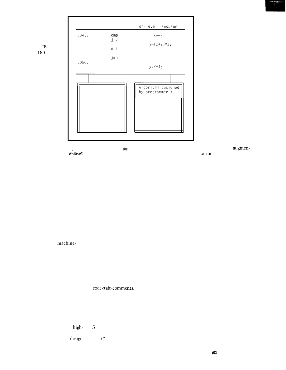
ments are gathered into
groups called blocks,
delimited by curly
braces. The execution of
each block of statements
is controlled by
THEN-ELSE,
WHILE, WHILE, FOR,
and SWITCH constructs,
depending on the
function of the program.
Most procedural lan-
guages have many or all
of these constructs. The
primary point is that
they allow the control
and collection of state-
ments into groups which
themselves may be so
grouped, permitting the
orderly expression of
hierarchical algorithms.
The second impor-
tant characteristic of C
and most high-level
languages is that the
Assembly
H
add
mov
shl
mov
if
else
Algorithm coded by
programmer Y.
Algorithm details
not distracting.
Test using same
routines as for HLL
implementation
Algorithm designed
and tested before
assembly coding
starts.
Test using HLL
comoiler.
Figure
l-Divide-and-conquer assembly language programming. The high-/eve/
algorithm on the right is separated from low-level assembly language implementation
programmer usually does not have to
know anything about the host
computer’s assembly language to
implement an algorithm. This charac-
teristic means the programs are
somewhat machine independent. You
guessed it-we are going to try to
make assembly language programs
more portable.
SWEET AND SIMPLE
The technique described here
involves writing an assembly program
in two easy steps. First the program is
written in a structured,
independent high-level language, and
then hand compiled into assembly
language for the target processor. The
text of the high-level language be-
comes the commentary for the
assembly program. Your brain takes
the place of the computer-based
compiler.
This discipline (oh, that word
again) has a number of advantages. The
main one is that the algorithm can be
conceptually separated from its
implementation on a particular
microprocessor. In other words, since
the algorithm is completed in a
level language version before assembly
coding starts, the programmer
instruction. Such prattle
is a waste of printer
ribbons and owl habitat.
Many programmers
use flowcharts faithfully
when writing programs,
maintaining them as the
development of a
program progresses.
Though this is a good
method, I believe the
technique presented here
is better for complex
programs, because the
documentation resides
with the assembly code
and is in structured form.
Large flowcharts usually
have mazes of intercon-
nections which some-
what preclude block
structure and encourage
spaghetti code program-
ming. However,
of this technique
with a flowchart im-
ing the algorithm need not be too
concerned about the details of the
microprocessor-details which can be
very distracting. This step allows the
programmer to concentrate more on
the details of the algorithm. This
method is the familiar divide-and
conquer-approach, with the division
taking place vertically, if you will,
between the operand and comment
fields on the assembly listing. See
Figure 1.
Another advantage of this tech-
nique is the improvement of program
documentation due to the built-in
structure. Sometimes I have wished for
a good bit of pseudocode to give me a
bird’s eye view of how someone else’s
assembly program works, rather than
sighting down a hundred pages of the
two black monoliths made of a
seemingly endless column of
This method
provides that extra information quite
naturally and displaces the flat
comment-per-line documentation
technique. In fact, the result is usually
fewer but more meaningful program
comments. Gone are pearls like, “add
to accumulator” on an add-immedi-
ate instruction, or, “is accumulator
zero
on a conditional branch
proves documentation as far as a
general functional overview is con-
cerned.
For the remainder of this article,
I’ll describe the details of the tech-
nique. It is presented as a series of
steps.
STEP 1.
Fully define the algorithm or task
that you wish the computer to per-
form. This sounds obvious, but many
programmers start typing mnemonics
before they have finished defining the
problem and its proposed solution,
leading to spaghetti code and Bugs
From Hell for other programmers to
battle. Flowcharts, state transition
diagrams, data flow diagrams, data
structure maps, and so forth, are the
net results of this step.
STEP 2.
Choose a programming language
in which you will express your
algorithm. I suggest that it have all the
constructs cited above for C, but that
is not absolutely necessary. It is best to
choose the structured language with
which you are most familiar, although
pseudocode (structured English) can be
used.
The Computer Applications Journal
Issue February 1994
41
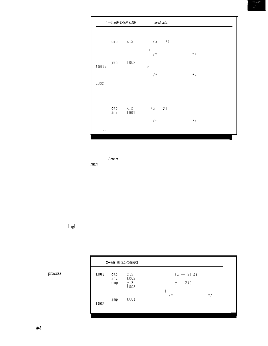
STEP 3.
Express your algorithm in the
high-level language or pseudocode. To
make the task easier and the program
more readable, don’t use any struc-
tures that you wouldn’t want to code
in assembly.
For example, I avoid ten-dimen-
sional arrays and other similar beasts
such as structures of arrays of struc-
tures, and so on. It is also best to
express a complex mathematical
operation as a series of simpler ones
for clarity, with an eye toward using
registers as temporary variables. Some
data structure purists may wish to be
more bold.
Indentation of program blocks is a
key aid to program readability. And
comment your high-level language
code; it sounds ridiculous, but hard
disk storage space on your PC is
cheap-your time is not.
STEP 4.
Onceyouhavecheckedoveryour
high-level language implementation
and tested key algorithms by compil-
ing and running them (if you have the
high-level language compiler), you are
ready to start assembly coding. Extract
identifier names and their memory
requirements from your algorithm and
allocate space for variables in assem-
bler. It is important that all major
variables and data structures be
defined and organized before you go to
the next step.
STEP 5.
Next, hand compile your
level language program into the
assembly language for your target
machine. It sounds complicated, but is
actually very easy. You don’t have to
know how the algorithm works to
compile the program. The algorithm is
contained in the high-level language
version and need not be disturbed
during the coding
In fact, I
have assembly coded programs which
another programmer has pseudocoded
with good results.
Start the compilation process by
converting your pseudocode to
assembly comments, typically by
adding a few tabs and a comment
character to the start of each line.
Listing
and IF-THEN
F-THEN-ELSE
jnz
LOO1
IF-THEN
LOO
if ==
statement block
se
statement block
if ==
statement block
Then place labels on all branch
destinations (see below for details).
The form
is convenient, where
is a three-digit number. Adjust the
label style to suit your needs and
tastes. Descriptive labels are used only
for subroutine and variable names.
They are not needed in general because
you can follow the indentation of the
pseudocode to find branch destinations
very quickly. This also eliminates the
confusion of cryptic labels, meaning-
less to any but the original program-
mer, and then only for about ten
minutes.
Next, add the assembly code. Each
of the basic constructs mentioned
above has a simple rule for compila-
tion. The following examples use C as
the high-level language. The mnemon-
ics used in my examples are those of
the 80x86 microprocessor.
IF-THEN-ELSE
See Listing 1. The conditional part
of the statement is checked starting on
the line containing the IF keyword. If
the condition is not met, control is
transferred to the line containing the
ELSE keyword matched with that IF
keyword. If the condition is met, the
THEN code block executes and a jump
instruction just before the ELSE
keyword transfers control to the end of
the IF-THEN-ELSE statement. The
program falls out of the ELSE code
block to the same point at the end of
the IF-THEN-ELSE statement. Labels
are required on the ELSE keyword and
after the end of the ELSE block.
Listing
;wh
jnz
ile
= =
statement block
4 2
Issue
February 1994
The Computer Applications Journal
WHILE
See Listing 2. The WHILE loop
construct tests the continuation
condition at the start of the loop. The
loop can therefore execute zero or
more times. A branch instruction at
the end of the enclosed block of code
always transfers control back to the
top of the loop for testing of the
continuation condition. The com-
pound conditional tests of x and y in
Listing 2 are coded separately for
readability.
DO-WHILE
See Listing 3. The DO-WHILE
looping construct tests the continua-
tion condition at the end of the loop.
The loop executes at least one time. A
branch instruction at the end of the
enclosed block of code transfers
control back to the top of the loop if
the continuation condition is true.
FOR
See Listing 4. The FOR construct
is a special case of the WHILE con-
struct where the loop continuation
condition is derived from the value of
a variable which is modified upon each
pass through the loop. You can
implement the more complex FOR
conditions that C allows by changing
the continuation test and
I NC X
instruction accordingly. Also, some
processors have special
jump instructions which can trim
down the code size some.
SWITCH
See Listing 5. The SWITCH
construct allows the selective execu-
tion of one of a number of statement
blocks depending on the run-time
value of a single variable called the
control variable.
The w i t c
h
state-
ment consists of a sequence of com-
parisons of the control variable against
constant values. Associated with each
constant is a block of code to be
executed when the control variable
equals the constant. The comparisons
occur in written sequence until a
match is found, at which time the
associated block of code is executed.
Some C compilers search the cases
bottom-up or use jump tables, but I
like top-down searching for ease of
PAL
GAL
EPROM
EEPROM
FLASH
MICRO
XC1 736
PSD
5ns
Free
software updates on
BBS
Powerful menu driven software
up
to 128 Channels
up to 400 MHz
up to 16K Samples/Channel
Variable Threshold Levels
8 External Clocks
16 Level Triggering
Pattern Generator Option
LA12100 (100 MHz, 24 Ch)
LA32200 (200 MHz, 32 Ch)
LA32400 (400 MHz, 32 Ch)
$2750 LA64400 (400 MHz, 64 Ch)
Price is Complete
Pods and Software
included
Software
200
sampling Rate
2 Analog Channels (2 ch. Digital Oscilloscope)
8 Digital Channels (8 ch. Logic Analyzer)
125 MHz Single Shot Bandwidth
up to 128K Samples/Channel
Call (201) 808-8990
I
Link Instruments
369
Passaic
Ave, Suite 100, Fairfield, NJ 07004 fax: 808-8786
The Computer Applications Journal
Issue
February 1994
43
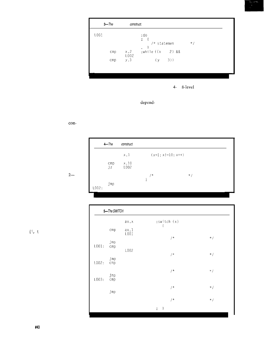
reading. If no match is found, a
DEFAULT block of code is executed.
Placing the most-likely executed cases
at the top of the construct will speed
the average execution time. And by all
means, use jump tables if you need the
speed.
AN EXAMPLE
use any CPU registers. First, the buffer
Let’s
look at an example. Say we
need a routine to sort a buffer of 256
bytes in ascending order and sort time
declaration looks like:
is not important. We are given the
address of the buffer and permission to
buffer ds 256
Listing
DO-WILE
LOO2
==
jnz
==
jz
LOO1
block
CONSIDERATIONS
with or
hardware stacks are
Listing
FOR
mov
;for
1001:
statement block
inc
X
LOO1
not amenable to stack-based parameter
passing and CPU registers or RAM
must be used.
We assume it exists prior to the entry
of our routine (it is global) and
tains 256 bytes of unsorted data.
Since the data design has been
Going further, procedures and
functions are handled differently on
each type of microprocessor,
ing on the stack capability. Processors
with a stack-indexed addressing mode
make stack-based parameter passing
easy and efficient. At the opposite end
of the scale, control-oriented micros
Due to these variations in archi-
tecture, uniformity in parameter
passing is not possible as it is with the
other control structures, so I will not
consider it further here except to stress
done, we proceed to the rest of the
problem: the design of the algorithm.
A simple, double-loop, byte swapping
scheme will do nicely. There. Now
step I-algorithm design-is complete.
I have chosen C for the high-level
language and the coded algorithm is in
Listing 6. That completes step
choosing a programming language.
It took just a few minutes to
scratch that out and type it in. I
compiled this program with a Turbo C
compiler and tested it with sample
data to decrease debug time. With
little effort, step S-coding the
algorithm-is now complete.
Listing
construct.
Examining the code regarding
variable space needs, I see three
variables
j,
emp) which I can
easily fit into CPU registers. This is a
convenient situation because no
memory space is needed for these local
variables. Now step 4-data space
allocation-is complete. The hand
compiled version of the routine is
shown in Listing 7.
You can see from this example
that the indentation leads the eye
quickly to branch sources and destina-
tions, showing the basic structure of
the program. Comments have been
added indicating which registers are
used for variable storage. This example
program is ready to assemble and
debug, completing step 5.
mov
case 1:
jnz
statement block
LOO5
break:
ax.3
case 3:
jnz
statement block
LOO5
break;
ax,4
case 4:
jnz
LOO3
statement block
LOO5
break;
ax,8
case 8:
jnz
LOO4
statement block
LOO5
break;
L004:
default:
statement block
break;
L005:
44
Issue
February 1994
The Computer Applications Journal
the importance of consistency within a
program. Comments at the start of
each procedure or function should
indicate values of input and output
variables, how they are passed, and the
operations performed on them.
One disadvantage of
generated code is that it is usually not
as efficient as that generated by an
experienced programmer. The tech-
nique described here likewise intro-
duces some code inefficiency. In
deeply nested structures, one may find
branch instructions that branch to
branch instructions. But this adds
little to program size and preserves the
basic block structure that is one of the
goals of this technique. However,
memory restrictions may well dictate
the elimination of every nonessential
instruction in some situations. I have
certainly had my back against the
ROM wall and compromised in this
area.
I have found program changes to
be much simpler using this program-
ming discipline. If a particular block
must be rewritten, it is deleted,
replaced with new pseudocode, and
assembly coded. The block structure
guarantees that there are no execution
paths other than through the top and
bottom of each block, so any block can
be removed and coded again without
worry of affecting another part of the
program that might have used a piece
of the deleted block. In short, the
block structure eliminates any
“spaghetti code” perils. The D-word
(discipline) is very important here, for
an ounce of spaghetti is worth a pound
of curses.
Program porting is also aided with
this programming technique. It is easy
to use a word processor to strip the
assembly code from a working pro-
gram and recompile it for a different
processor, either by hand or with an
actual compiler. Most of the data
structures will remain unchanged
during the translation, too, speeding
the task.
You will find that nested IF
statements will produce multiple
labels on one instruction. You might
be tempted to remove all but one, but
don’t because the multiple labels make
it easy to insert new code (another
Listing
C coded
algorithm can be tested using a C compiler eliminate logical errors before
assembly coding. Remaining bugs in fhe assembly version are limited
not
algorithm.
void sort void0
This function sorts a list of 256 bytes in ascending order.
The
is a global variable and is assumed to be filled
with data. A double loop swap sort is used. Register values are
undefined at entry and exit.
int i,
buffer index
j
buffer indes
char
temp
used in byte swapping
double loop compares each pair of bytes
for
for
if
compare pairs of bytes
swap the bytes
end of sort0
Frame Grabber
l
$495 Including Software with “C” Library
l
Half
Card for Compact Applications
l
Real Time Imaging with Display Output
l
8 Bit (256 Gray Levels)
The Computer Applications Journal
Issue
February 1994
45
ELSE
clause,
for example) at a later
date without affecting other branch
destinations. Remember, labels are
cheaper than your time.
You may also use assembler
macros to ease the coding process,
though the examples in this article do
not.
Since there is no external author-
ity imposing discipline on the pro-
grammer using this system (as a
compiler would), each programmer
will use it a little differently. This is
okay. The main goal is to foster a
consistency of style and structure,
first to increase productivity, and
second to allow following program-
mers to understand the subject
programs.
In conclusion, the advantages of
this method are the separation of the
algorithm from the assembly language,
improvement of documentation
through the use of structured com-
ments, and improved mental health of
your successors. The first item saves
time now, the second later, and the
third may save your life.
I have used this discipline to write
numerous assembly language programs
for ten years on and
machines with considerable success
and positive comments from other
programmers. I adopted the technique
after writing programs using other
methods and have noticed a dramatic
increase in productivity, ease of
program development, and consistency
of documentation. I hope this method
allows you similar profit.
Hank Wallace is the owner of Atlantic
Quality Design Inc., a consulting firm
located in Rural Hall, N.C. He has
designed embedded system software
and hardware in the areas of data
collection, machine control, micropro-
cessor emulation, satellite and mobile
radio communications, radiopaging,
manufacturing test, and speech
privacy.
410
Very Useful
411 Moderately Useful
412 Not Useful
Listing
7-Assembly coded sorting
the block
of the program and
allows
of
For
the assembly codecanbe
strippedand the program recompiled, eitherbyhandorbycomputer.
This function sorts a list of 256 bytes in ascending
order. The
is a global variable and is assumed
to be filled with data. A double loop swap sort is used.
Register values are undefined at entry and exit.
int
buffer index, register SI
buffer index, register DI
char temp:
used in byte swapping, register AH
small
extrn
buffer
sort:
mov
buffer
mov
mov
bx,offset buffer
double loop compares each pair of bytes
mov
jnb
LOO6
mov
inc
jnb
di,si
di
mov
jbe
LOO4
mov
mov
mov
mov
L004:
inc
inc
LO06:
ret
end
di
si
LOO1
i++)
for
if
compare pairs of bytes
swap the bytes
end of sort.0
46
Issue February 1994
The Computer Applications Journal
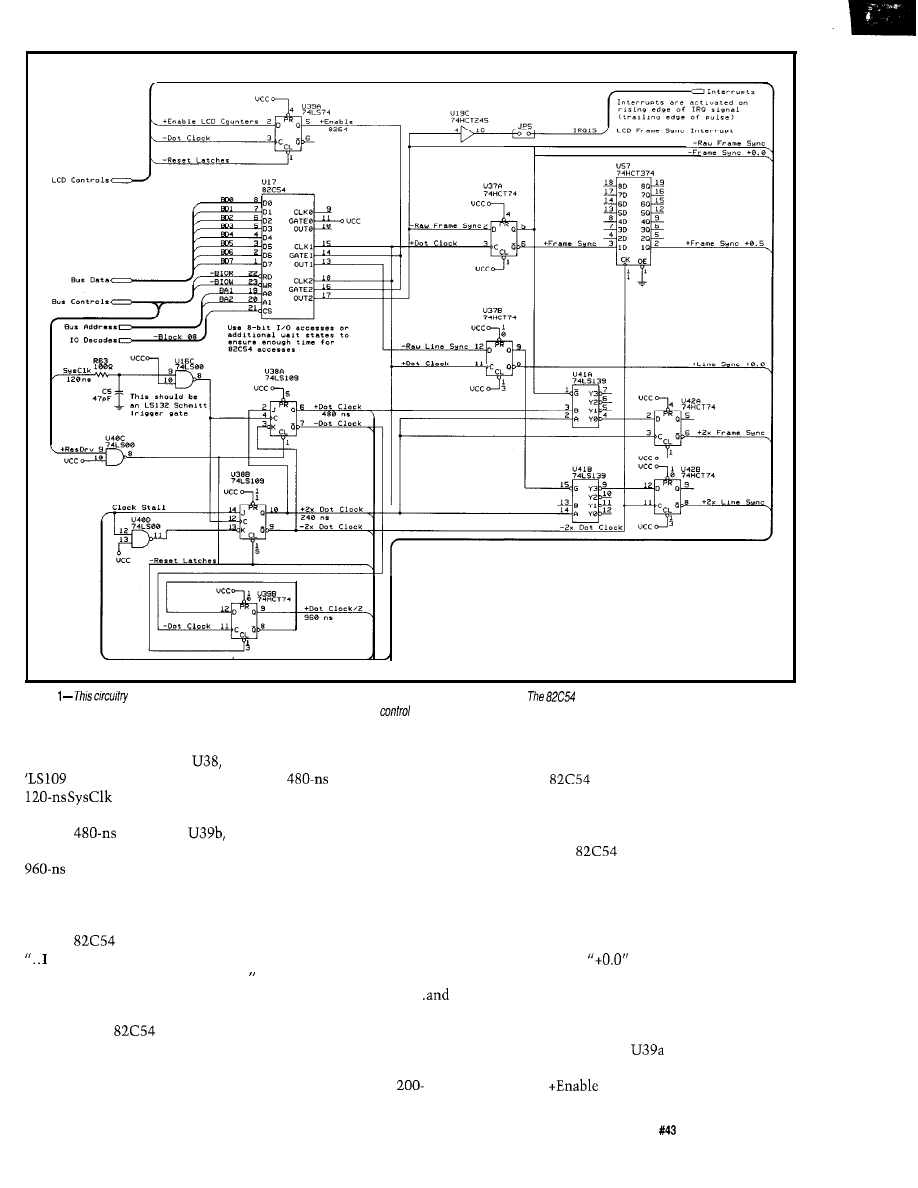
Figure
defines the fundamental Dot Clock period that drives the rest of the Graphic LCD Interface.
was covered in a previous column, but its clock
and gate lines have changed. The various Dot Clock and Sync signal outputs can
a variety of panels.
The ISA bus SysClk signal defines
the basic interface timing.
an
dual J-K flip-flop, divides the
by two to produce the
double-speed 2xDot Clock and the
regular
Dot Clock.
part
of an ‘HCT74, produces the half-speed
Dot Clock needed for slower
panels.
Back in Issue 34 (May 1993) we
got the Firmware Development
Board’s
working. I said then,
may come up with other applica-
tions that require a wiring change..
and you’ll be pleased to know that
this is just such an occasion. U17 in
Figure 1 is the
you’ve already
checked out, with two channels now
devoted to metering out Dot Clock
cycles.
Counter 1 produces the -Raw Line
Sync signal by counting the number of
Dot Clocks in each LCD row.
The 640x200 and 640x400 panels I
have require either 160 or 320 clocks
per row, depending on whether they
have a single- or double-speed inter-
face. Other panels have different
requirements, so it made sense to use a
programmable counter rather than a
bunch of jumpers and gates.
Yes, I know it’s inconsistent to
talk about LCD
rows
and Line Sync
signals. That’s the way my notes and
sketches started out..
it’s too late
to change now!
Counter 2 controls the number of
Dot Clock cycles in one LCD display
frame by generating the -Raw Frame
Sync signal. Both
and 400-line
panels require 32,000 clocks, but other
panels need different counts. Here, the
serves as a compact 16-bit
programmable counter.
Figure 2 is a diagram timing for
the key Graphic LCD Interface signals.
The
timing specs say the
output delay may be up to 100 ns after
the falling Clock edge, so you can’t use
the signals for critical timings.
I
use an
‘HCT74 to synchronize the edges with
+Dot Clock; the resulting pulses occur
at the
times relative to the rest
of the signals.
Both channels must start counting
on the same Dot Clock cycle so that
the two sync signals have the right
relationship.
disables the
counters until the firmware sets the
LCD Counters bit in the LCD
The Computer Applications Journal
Issue
February 1994
4 9
Data Acquisition
Control Solutions
Temperature Measurement
Solution Package $895
Features:
For J, B, R, E thermocouples
8 thermocouple
expandable
to 32
resolution with
A/D
Up to 250 samples per second
16 D/I and 16 D/O channels
Windows SCADA
Icon based, no programming required
1 General Purpose DAS Card
$295
8 A/D,
D/A,
DIO,
wiring kit
1 Multifunction DAS Card
$395
16 A/D. 2 D/A, 32 DIO, counter
1 High Performance DAS Card
$595
programmable gain
1 24 Ch Digital
Card
1 24 Ch Digital Input w/Interrupt
$180
7 32 Ch Digital
Card
$170
32 Ch Digital Input w/Interrupt
$235
Ch Digital
Card
$295
1 8 Relay 8 Digital Input Card
$210
1 High Speed Data Streaming Pkg.
$595
data streaming to disk
1 PC Strip Chart Recorder Pkg.
$695
channel recording at
Remote DA&C Starter Kit
$495
RS-485 based, up to 4000 feet
Free
Solution Guide
for quality minded,
bugdet conscious
Engineers
750 East Arques Ave. Sunnyvale, CA 94086
Tel: (408) 245-6678
FAX: (408) 245.8268
Control port. When
clock rises,
both
Gate inputs go to a high
state and the counters are off and
running.
While I was debugging this
circuitry, the LCD panel would
occasionally go blank. It turned out
that Counter 1 stopped counting
unpredictably for periods between a
few cycles and a few hundred millisec-
onds. This immediately threw off the
critical timing between Line and
Frame Sync. The
Gate input
remained high and Dot Clock contin-
ued to run during the stoppages.
The
has one of those
classic “you must read every word”
data sheets. The Clock input timing
specs include this tiny footnote: “Low-
going glitches that violate
may cause errors requiring counter
programming.” Translated into
English, this says that if the clock isn’t
perfect the counter will misbehave in
strange and mysterious ways. That
footnote accounts for the RC filter and
gate driving U38.
We think of TTL logic devices as
digital: their outputs are either high or
low, never anywhere in between. In
reality they are analog circuits with a
nonlinear transfer characteristic. If the
input voltage is between the valid
logic and logic 0 levels you
will
get
something out, but it won’t be a
Boolean value.
Dot Clock was not the perfect
square wave I expected. Once in a
while the high half-cycle was dented
by a low-going glitch. After some
delicate probing I discovered an
impressively noisy SysClk signal on
the backplane bus. The clock noise
was bad enough to force the
latches into metastable states and the
ensuing invalid outputs stunned the
counters. While they didn’t
need reprogramming, they sure didn’t
work right!
The correct solution for this
problem is a Schmitt trigger gate in the
clock path. Unlike a standard logic
gate, a Schmitt trigger has analog
feedback that modifies the input
switching levels. As a result, most
glitches simply Go Away. But I didn’t
want to add an ‘LS14 just to get one
inverter.
So I used a simple RC filter to
knock off the noise and a spare ‘LSOO
gate to square up the result. Yes,
I
know I could have substituted an
‘LS132 Schmitt trigger NAND), but
the other circuits using that package
couldn’t stand the additional delay. An
RC filter is not a textbook solution,
but it works for my application. Take a
look at your SysClk, then tell me what
you see and how you attack the
problem.
Rest assured it took me much
longer to discover and solve that
problem than to write about it!
Although the
defines the
overall row and frame timing, its
output pulses cannot drive the LCD
panel directly. The dot data and sync
signals must both arrive with the
correct polarity at the proper times, so
we now consider the dots.
A CHAIN OF DOTS
A
SRAM holds the
binary data that will become dots on
the panel. The RAM, U45 in Figure 3,
is time-shared between the ISA bus
and the LCD panel. Obviously only
the PC can write to it, but both
circuits can read the dot data. The Dot
Clock signal determines which
circuits have access to the RAM at any
given time.
The LCD Address Counters, U43
and U44, provide the
address for
each RAM byte when the LCD is in
control. Each
chip contains an
S-bit counter followed by an
latch
with tristate outputs. The counter and
latch are both driven by -Dot Clock,
so they change state on the falling edge
of +Dot Clock. In this application, the
Address Latch is always “one behind”
the Address Counter because it
captures the count just before the
clock edge.
Frame Sync clears the counters to
zero at the beginning of each panel
refresh. The actual reset signal occurs
during only a quarter of the Dot Clock
period to ensure that the counter will
step from 0 to on the next clock
pulse. Figure 2 shows the timing: the
reset pulse must be finished by the
next -Dot Clock rising edge
The
Address Latch solves a
critical timing problem: the path
5 0
Issue
February 1994
The Computer Applications Journal
length from the Frame Sync reset logic
through the counters and RAM into
the LCD Data Latch is longer than 240
ns. Latching the address provides a
stable signal for the entire LCD half of
Dot Clock, while delaying the RAM’s
output data by one cycle.
The RAM address alternates
between the Address Latch and the
address on the PC’s ISA bus connector.
The
outputs are active when
+Dot Clock is low, while U46 and
U47, the PC Address Buffers, are active
when -Dot Clock is low. Figure 2
shows the sequence of events; note
how the LCD Address Latch ensures
that the address remains valid while
the counter is being reset.
The LCD Data Latch, U48,
captures the RAM output when Dot
Clock goes high 240 ns after the
LCD’s half cycle begins. This ensures
stable data at the LCD panel when Dot
Clock goes low 240 ns later. The
panels have various timing specs, with
some requiring at least 150 ns of setup
and hold time. Without this latch, the
data at the LCD panel would disappear
long before the panel was done
capturing it.
OFF BY ONE...
Pop quiz: According to the
LCD panel specs, when does the Frame
Sync pulse occur in relation to the first
row of data? (2) In Figure 2, what is
the RAM address of the value in the
Data Latch when Frame Sync is
active? (3) How do you resolve this
paradox!
Answers: (1) After 160 Dot Clocks,
at the start of the second row of panel
data. (2) 31,999, plus or minus one
depending on how you read the
diagram. (3) Ah, Grasshopper, consider
the sound of one hand clapping..
forehead.
Figure 4 is the
DMF651
640x200 panel pulse timing diagram,
redrawn using my nomenclature.
There are three vital synchronizing
relationships: Line Sync/Dot Clock,
Frame Sync/Line Sync, and Alternate
Frame/Line Sync.
The falling edge of Line Sync must
be more than 80 ns away from a falling
Dot Clock edge.
delays the
-Raw Line Sync output until
the next rising Dot Clock. Figure 2
shows that
Sync+O.O rises when
the last data byte in each row appears
in the Data Latch and falls on the first
byte of the next row.
Frame Sync must be high for at
least 100 ns on either side of the first
Line Sync’s falling edge.
synchro-
nizes -Raw Frame Sync to the next
rising Dot Clock and U57 delays it
by half a Dot Clock cycle. Figure 2
shows the result: the pulse called
is neatly centered
on the falling edge of
Sync+O.O
with about 240 ns setup and hold
times.
The Alternate Frame signal comes
from U52 in Figure 5. For the DMF65 1,
this signal must change state within
300 ns of a Dot Clock falling edge, so I
clocked
with
The Hitachi LM215 refers Alternate
Frame to the falling edge of Line Sync
rather than Dot Clock, so a jumper
allows you to use -Frame Sync+O.O
instead.
U41 and U42 generate the sync
signals needed for panels that accept
data every 240 ns. The double-speed
2xDot Clock changes the allowable
width and alignment of the sync
signals, but the basic Graphic LCD
Interface hardware remains the same.
The firmware sets up the LCD Data
Multiplexer to switch between the two
nybbles every half Dot Clock cycle, so
the data arrives on time. I’ll go into
more detail later.
You must drive all LCD signals
with CMOS logic gates to meet the
panel’s minimum
Because I
used several spare gates from other
sections of the
logic, some of
the LS gates mentioned in previous
columns are now HCT. In actual
practice, LS gates will probably work,
but only by the grace of good
tolerances..
is bad practice.
PORTING A RAM
When Dot Clock is high, the PC
controls the Graphic LCD Interface
RAM. U46 and 47, the PC Address
Buffers, are enabled during that
cycle. U49, another ‘LS245, shuttles
PC data to or from the RAM. These
buffers are in series with those already
on the FDB.
ICE?!!!
Yes, that’s right! HTE has dropped the
price of it’s popular 8031132 Enhanced
from $269 to $149. Now you
can’t afford to be without one! This
ICE performs single step, real-time
execute to breakpoint, disassembly
a n d m o r e . u s e r c o d e s p a c e ,
expandable to 32K. Order yours today!
More
ICE
Our
Plus has so many features
the price is unbelievable. 48K of user code
space,
real-time
execution,
expandability to nearly all of the 8051
family
processors. We
are
now
supporting pods for the
8751.
a n d
W i t h p o d s
at only $149, going to a different.
integration processor is easy. Pod
base unit are just $448 complete!
At $149, our
OEM board has
the price and features you need right
now! It’s an 8051 core processor with an
eight channel,
AID, two PWM
capture/compare registers, 16
one RS232 serial port, four
JEDEC memory sockets. Add options like
t w o m o r e
ports, 24
nore digital
real-time clock, serial
EEPROM, and battery-backup for clock
RAM. Start with the Development
all the peripherals and a debug
nonitor for only $349. Download and
your code, assembly or ‘C’, right
the SBC, then use the low-cost OEM
of your choice for production. We
do customs call for a free
SBC
NEW! Starting at only $249. Two serial
Parallel, expand to 16
12-bit A/D, 8 ch. 12 bit D/A, Keybd,
Relay
more. Call for details!
(619) 566-l
70662.1241
The Computer Applications Journal
Issue February 1994
51
+2x Dot Clock
+Dot Clock
-Raw Frame Sync
\
-Clear Counter
32000,
Address Counter
3 1 9 9 8 X 3 1 9 9 9
0
1
2
. . . 159
160 161
Address Latch
31997x
31998 31999
0
1
158
159 160
RAM Address
PC 31998 PC 31999 PC 0
PC
PC
2
PC 159
PC 160 PC
Data Latch
3 1 9 9 7 3 1 9 9 8 3 1 9 9 9
0
158
159 160
Sync +O.O
Sync
\
-Raw Line Sync
Sync +O.O
\
\
Alternate Frame
For 240ns Panels:
31997 31998 31999
0
1
. . . 158
159 160
LCD Data
4.7
0’3
4.7
0’3
47
4 7
0.3
4’7
0 3
X
4’7
X
0’3
X
4-7
+2x Frame Sync
+2x Line Sync
Figure
timing diagram summarizes the Graphic LCD Interface’s operation. The
RAM holding the LCD
patterns is time-shared between the PC ISA bus and
the LCD circuitry. The -C/ear Counter signal resets LCD Address Counter at the end of each frame of data;
signal originates in the
counter described in an earlier
column.
There is one catch in the PC’s
access: the Dot Clock cycle is not
synchronized with the ISA bus read
and write cycles. If it goes low at the
end of a bus read, the CPU will get
invalid data or write junk into the
RAM because the PC’s buffers are
turned off and the LCD circuitry is in
control.
Solving this problem means the
PC must wait until Dot Clock goes
high or the LCD panel must wait until
the PC is finished. I chose the latter
course because you can pause an LCD
clock for a very short time without
visible effect.. .and the PC access is
slow enough already. You can do it the
other way if you like.
Photo
1
shows how this works.
The top trace is -SMemW, which
controls the ISA write cycle timing.
The lower trace is Dot Clock, which is
normally a
square wave. Notice
that it’s always high when -SMemW
rises, even though it’s not synchro-
nized when the cycle begins. The
normal clock cycle resumes after
-SMemW ends.
A complete
ISA bus memory
write is six SysClk cycles long, with
-SMemW active for about the last 4.5
cycles. Because Dot Clock is four
SysClk cycles long, the maximum
delay until Dot Clock goes high after
-SMemW becomes active is three
SysClk periods.
monitors the double-speed
2xDot Clock, Dot Clock, and the
(negative active) OR of -SMemW and
When Dot Clock goes high
during a PC access,
output
freezes the SysClk divider flip-flops
and holds them until the PC is
finished.
The shortest RAM access is thus
about 1.5
Allowing for the
buffer delays, a
RAM is just
about fast enough. I suspect some
systems may need a
RAM or
74F buffers instead of 74LS parts. In
any event, work out your system’s
timings and see how close am.
At worst you can add a wait state
or two to the PC access. Don’t make
the mistake of stalling both Dot Clock
and the PC, though; if both sides of
the interface are stopped, neither one
will restart!
Even though a Dot
cycle
can be stretched by up to
52
issue February1994
The Computer Applications Journal
when it collides with a PC access, as
long as this is relatively infrequent
you’ll never see it. One of my test
routines writes data into the RAM
while toggling a parallel port bit to
provide scope sync: one byte every 33
affects an invisible 1.5% of the Dot
Clock cycles.
On the other hand, another test
routine has a REP LODSB in a loop that
reads all 32K bytes at 960
That
severely
distorts the Dot Clock
cycle, holding it high for 720 ns and
allowing only one
low
cycle between each access. The
resulting refresh rate drops to 33 Hz
and the panel develops an obvious
flicker.
But remember, even if you used
REP MOVSB
to
read or write all 32K
bytes, you wouldn’t do it a loop. The
LCD panel’s optical response is in the
range, so it wouldn’t have
time to respond to 30 ms of furious
writes; the new dots would take
another hundred milliseconds or so to
replace the old ones! Stop worrying.. .it
works OK.
Do note, however, that this
interface isn’t suited for DMA or
mastering card access because the
timings depend on the relation
between
and -SMemR/W,
which is valid only for system board
accesses. If you need a more versatile
board, check
book for the grim
details.
Even when all your logic is
working correctly, you won’t see
anything on the LCD panel unless you
apply the right drive voltages.
I
won’t
mention how often I’ve caught
palpitations at the sign of a blank
panel only to realize the power supply
lead was dangling.
PRACTICAL POWER
The power supply circuitry that is
shown in Figure 5 is overkill. You
really only need perhaps 20 or 30
at a single voltage, so there’s no need
for a bulky wall-wart transformer, a
huge capacitor, and a
watt voltage regulator in a TO220
case. Suffice it to say there are easier
and more compact ways to generate
drive voltages for an individual LCD
panel.
But if you’re working with a
supplies? Maybe he’ll even include
variety of panels, it makes sense to use
backlight inverters!
parts from your stash for a versatile
is my concession to the power
supply. Maybe one of these days we
sequencing specifications found in the
can convince Jeff to do a “From The
data sheets. Most of the panels are
Bench” column on LCD power
happy if you apply V first and
Photo l--An
bus
read or
access forces Dot Clock
in fhe high
is
The
fop trace,
is active for about 4.5
cycles.
Clock, shown in the
trace, is
not synchronized
when the write
begins, so if may
at any of the four times shown in this
exposure. The RAM access
when Dot Clock goes high and ends when
W goes high, which is
just enough fime for a
RAM cycle.
Drop
into
Your Application
Don’t worry about which
microcontroller to choose
when you can rely on the
industry leader.
S M A L L
AND
PERFORMANCE.
-ADD ONLY THE
LOWERING
AND MACRO
AVAILABLE
PRICES START AT $59 IN
Micro Wonders
3 2 0 B r o w n S t S u i t e 4 0 4
West Lafayette, IN 47906
1686
The Computer Applications Journal
Issue
February 1994
5 3
HAM may be
accessed by
the ISA bus and fhe LCD Address Counters. The -LCD Address Match signal is produced by a
comparator similar
one shown in
36.
Dot Clock signal controls three-state buffers driving fhe RAM’s address lines.
‘LS139 decoder generates two signals
depend on the Dot
Clock phase
other
of fhe circuit.
Figure
Opfrex
signal timing
specifications dictate
how Graphic LCD
Interface must operate.
Notice
fhe
and
Line Sync must be valid
on falling edge of
each Dot Clock pulse,
but Frame Sync is
related falling
edge of Line Sync.
Other panels have
different specs, but fhe
Graphic LCD Interface
can handle many of
fhem
a few jumper
changes.
Dot Clock
Data
Line Sync
min
1
min
min
Frame Sync
300ns
- - - - - - - - - _ _ _ _ _ _ _ _ _ I _ _ _ _ _ _ _ _ _ _
Alternate Frame
Issue
February 1994
The Computer Applications Journal
remove it last, which is what the
DPDT relay accomplishes by discon-
necting the LCD drive voltages. The
ISA bus
signal is active when
the power supplies are out of tolerance
or the system is reset, which ensures
V is always active first and last.
CAUTION:
set the LCD drive
voltage before you connect the panel,
then monitor a voltmeter when you
adjust it. The supply shown in Figure 5
can apply enough voltage and current
to destroy a panel with a twist of a
screwdriver. Be hypercautious here, if
nowhere else!
GREATER&LESSERARRAYS
The circuitry so far can handle
panels with
Dot Clocks. The
situation is slightly different for panels
needing
or
clocks, but
the hardware modifications are easy.
My board is festooned with jumpers,
but you can build only the parts
needed for your panel.
The Sharp
640x400
panel expects 320 Dot Clocks on each
of 200 rows with a
Dot Clock.
The RAM still delivers eight bits every
480 ns, so the firmware sets up the
LCD Data multiplexer to switch
between the two nybbles on each half
Dot Clock cycle. As a result, the
panel’s dots line up quite nicely with
the data bytes: the high and low
nybbles are contiguous at last!
The Frame and Line Sync pulses
are 240 ns long and synchronized
with the double-speed 2xDot Clock. I
used U41, an ‘LS139 decoder, to
control the two flip-flops in U42 with
the result shown in Figure 2. The
panel is driven by -2xDot Clock to get
a falling edge in the middle of each
nybble.
The Sharp LM641481 640x480
panel is similar to the
except that the extra 40 (not
rows
reduce the refresh rate to about 54 Hz.
This is another high-performance
panel with a brilliant cold cathode
fluorescent tube backlight. Unfortu-
nately, to my eyes that
refresh
flicker is quite obvious. As with the
the CCFT inverter is
really hard to find.
A 640x480 panel requires 38,400
bytes of RAM, which the standard
T
HE
I
N C R E D I B L E
N
E W
PE-8351 FX
I
N
- C
IRCUIT
E
M U L A T O R
$1451.00
n
supports
Fine Emulators
New Debugger
8X52/32,
From
Enhancements
n
Real-time and Nonintrusive
n
68HClt From
n
Full support for structures,
n
64K Program Memory
n
68HC05 From
unions, arrays, pointers
64K Data Memory
n
COPB From
n
Data structure
n
128K Hardware Breakpoints
n
More than 100 devices
browser/editor
Frame Trace Buffer
supported through
n
True expression in watch
n
Transparent Trace
changeable probe cards
window-detect bad pointers
(View Trace and Execute
Simultaneously)
Nobody Matches the Value of the PE Family
PE Product
Max
NOHAU
Easy Installation to
List Price*
List Price*+
RS232 Port of any D
OS
P C ,
8351 FX
1 6
$ 1 4 5 1
$4820
even Laptops!
8 3 7 5 1 1 7 5 2 1 6
8 5 1
4300
l
Built-In Self-Test
8032-24 24
8 5 1
4945
8032-42 42
999
7 1 9 5
n
symbolic Debug
‘U.S. Retail price.
Price
List dated
verbal quote
D e b u g
Our new AET Emulator
architecture
(Advanced Emulator Technology, Pat. Pending)
providesunmatchedvalue.
delivers
backguarantee,
periods, rental
free technical support. Call today
for
FREE demo diskette.
Corporation
Metatink Europe
325 E. Elliot Road, Chandler, A
Z
8 5 2 2 5
2,
Kirchseeon-Eglharting
Phone: (602) 926-0797 Fax: (602)
(08091) 2046. Teletax (08091) 2386
The Computer Applications Journal
Issue
February 1994
5 5
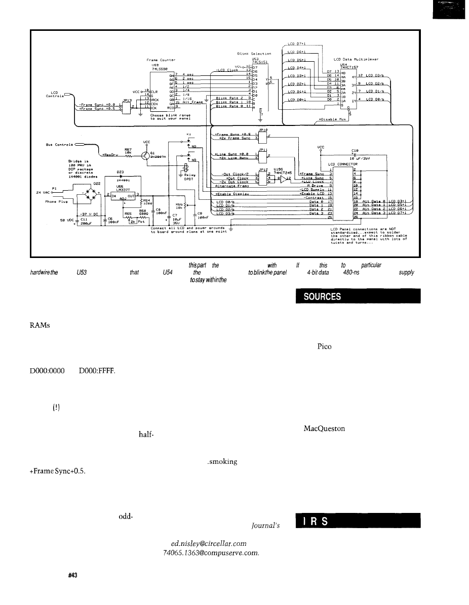
Figure
5-Because each LCD panel has different
requirements,
of schematic is festooned
jumpers. you build circuit drive a
panel you can
signals.
can select a signal
alternates
between nybbles of each byfe
if if uses
and a
clock. The power
can drive near/y any common LCD panel, but must be adjusted carefully
panel’s voltage specifications.
Graphic LCD Interface just doesn’t
have. Although it’s not shown on the
schematic, you can piggyback two 32K
with their -CE inputs driven by
+LCD Al5 from U44 and -LCD Al5
from an inverter. Disconnect ISA bus
address line A15 from the ‘F521 so you
can access all 64K bytes between
and
In contrast to that vast array of
dots, the Hitachi LM215 480x128
panel is electrically a quartet of dinky
240x64 arrays. Four data bits
arriving every 960 ns refresh it at
about 68 Hz. Each data bit drives a
separate quadrant so there are 240
speed Dot Clocks on each of 64 rows.
Use the -Dot Clock/2 jumper and run
the Alternate Frame divider from
The LM215 needs only 15,360
nybbles of data, thus the high-order
nybbles can be used for blinking as
usual. Because the panel runs at half
speed, the dots use only the
numbered bytes of the first 30,720
RAM locations. The test pattern for
this panel is a little different than the
others to cover all four quadrants.
RELEASE NOTES
The BBS code this month is
GRAPH LCD, even though I haven’t
discussed it. It wiggles the control
port, gives you manual control over
the 8254 counters, verifies the LCD
buffer with pseudorandom data, and
writes test patterns into the buffer so
you can see your wiring at work. I’ll go
into more detail next month, but you
should be able to puzzle out the
essentials on your own.
Be careful with that LCD power
supply! Use an ohmmeter to cross-
check the LCD pin numbering: the
supply voltages and grounds should
appear on the filter caps, right? As
the woodworkers say, measure twice
and cut once..
a new panel
can really mess up the rest of your
day.
q
Ed Nisley, as Nisley Micro Engineer-
ing, makes small computers do
amazing things. He’s also a member of
the Computer Applications
engineering staff. You may reach him
at
or
Last month’s column listed sources
for LCD panels and other hardware.
Check the latest catalogs to find
out what’s in stock now.
Electronics manufactures
ultrareliable DC-DC converters
that may come in handy if you’re
building critical LCD interfaces.
Unlike surplus parts, their Series A
single- and dual-output supplies
come with a pedigree and a price to
match, so don’t bother them unless
you’re serious. They’re at 453 N.
Pkwy., Mt. Vernon,
NY 10552, (914) 699-5514, fax (914)
699-5565.
Pure Unobtainium has the
complete Firmware Development
Board schematic and selected parts.
Write for a catalog: 13109 Old
Creedmoor Rd,. Raleigh, NC
27613, phone/fax (919) 676-4525.
413
Very Useful
414 Moderately Useful
415 Not Useful
56
Issue
February 1994
The Computer Applications Journal
Warming
Up the
Digital
Thermostat
Jeff Bachiochi
visited the Red
Cross this week-
includes a few tests: your blood pres-
sure, temperature, and extraction of a
drop of blood, just to make sure you
are in satisfactory condition. I noticed
that the usual electronic thermometer
was missing. In its place was a sanitary
piece of paper wrapped like a band-aid.
Once removed from its wrappings, the
strip is inserted under the tongue as a
thermometer would be. After a minute
or so it is removed and small spots
[which permanently change color at
various temperatures) indicate the
temperatures it has been exposed to.
Even though they are disposable, there
are some positive reasons to use them.
They are inexpensive, require no
power, are small in size,
and are light in weight.
They present a good ex-
ample of today’s technol-
ogy changing the way we
measure temperature,
even if it is not electronic.
Although a few com-
panies are now announc-
ing thermostatic
Dal-
las Semiconductor’s
DS1620 has what is
needed to take this idea to
the next step. As I dis-
cussed last month, the
DS1620 offers direct tem-
perature conversion thus
Photo
thermostat is
mounted below the old one it
replace. The temperature can be read
from across the room.
eliminating the conventional analog
conversion. It also allows a high and a
low temperature
to be ad-
justed through a clocked serial port.
These setpoints govern the hysteresis
signature of the output control bit
which has a
source/sink capabil-
ity. Please see last month’s column for
more of this chip’s particulars.
I chose the primitive
processor for this project for its low
price and availability. It has a single
timer and no interrupts, which should
prove interesting. The local control
and temperature display would fit into
the “single page”
device,
however adding a communication
interface would easily overflow the
5 12
words available to the ‘54.
My original concept was to have
the thermostat merely display the
temperature locally and pass on the
data to a centralized controller. The
controller would be responsible for
calling for heat and controlling the
individual zones. This meant if, for
some reason, the central controller
went down, so did the temperature in
the house. To avoid this, I added a bit
more sophistication to each thermo-
stat. Now, each can act independently
of the central computer, yet still be
commanded by the central controller
to take advantage of nighttime or
unoccupied temperature setbacks.
Issue
February 1994
The Computer Applications Journal
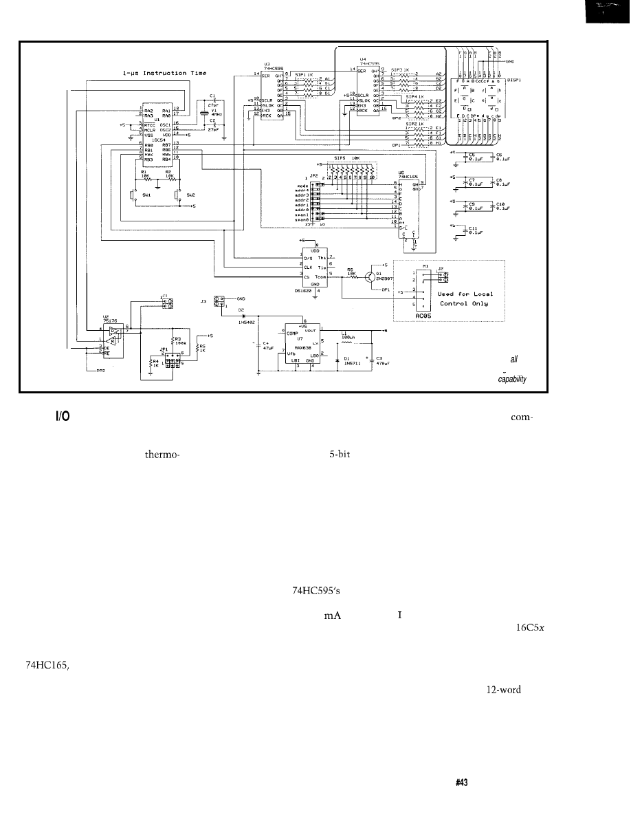
Figure l--By adding a processor to the
digital thermostat, you can add kinds
of
bells and whistles including local
display
and central control
LOCAL
the processor using the common clock
processor must reconfigure its
The PIC processor is responsible
line. The span sets the hysteresis
mon data I/O line as both an output
for five I/O operations. The first is to
setpoints from 1 to 4°C above and
and an input bit.
provide an interface with the
below the mean setpoint. The
The last I/O operation is commu
static device, the DS1620. The second
thermostat address is from 0 to 3 1
nication. A 75 176 RS-485 driver is
is the output to the digital display, and
the third is to capture input from the
configuration port. The fourth opera-
tion is to monitor user input through
two push buttons. These push buttons
could have been made part of the con-
figuration port, but I didn’t want to
have to read the port in each time to
check the status of the switches. Con-
sequently, they are tied directly to two
processor pins. The last operation is
communication with the central con-
troller. This is accomplished through a
half-duplex RS-485 network (Figure 1).
The configuration port, made from
a
cannot be tristated, so it
cannot share the common data I/O
line with the DS1620 and the display
port. Configuration data, which
consists of temperature span, thermo-
stat address, and display mode settings
on JP2, is loaded into the shift register
with a *Load strobe and shifted into
(that’s the maximum number of nodes
allowed on a ‘485 net). The display
mode selects between degrees Celsius
(the actual conversion) and Fahrenheit
(calculated from Celsius).
The display port shares both the
common clock and data I/O line with
the DS1620. It requires only a single
output bit to load the shift register
data (16 bits) into the
output display registers. The output
registers source only about 1
to
each of the 16 segments. This keeps
power dissipation down while still
lighting the digits. The left decimal
point indicates the thermostat is
asking for heat, while the right
decimal point shows network activity.
The DS1620 shares both the
common clock and data I/O line. It
also uses an additional CS (chip select]
output from the processor. Since data
is passed to and from the DS1620, the
used to assure noise-immune commu-
nication even at great distances. Only
three processor bits-TX, RX, and TX/
*RX enable-are necessary. RX
remains enabled until a properly
addressed message has been received.
A reply is then formulated and TX is
enabled only during the response. The
net is then free for additional traffic.
TWO-LEVEL STACK
do believe the stack implementa-
tion is the weakest point of the
series. Only two levels of calls can be
made without some major bending
over backwards. Another oddity is that
although you can make an
L CA L L or
L J U M P
to another page (5
group) and the page pointers within
the status register are correctly set, a
RET
will pull the complete 1 l-bit
address from the stack. However, in
this case the page pointers are
not
set
The Computer Applications Journal
Issue
February 1994
5 9
correctly from the three most-signifi-
cant bits. Argh!
With only two levels to work with
and knowing one of those must be
saved for the communication routine,
only one call could be made at a time
(no nested calls). This makes for some
lengthy code.
The DS1620 hands off tempera-
ture readings in degrees Celsius times
two. The “times two” comes about
because the least-significant bit of the
conversion is a
placeholder. If
the reading is shifted once to the right,
it can be directly interpreted as degrees
Recall that the Fahrenheit
conversion equation is = (“C x +
32. Here’s how I calculated for the
limited range of
l
Start the conversion with what is
output from the DS1620 [which is
actually C * 2)
*Multiply by 2 (shift left):
or
*Divide by 5:
or
*Add C:
or
5) or
32:
or
THE MAIN LOOP
After some initialization code, the
thermostat falls into an endless loop.
The loop consists of four functions.
First, it reads the current temperature
from the DS1620. Second, it converts
this Celsius value into a Fahrenheit
equivalent (if necessary), and also into
two decimal digits for display through
the
Finally, it checks the
push buttons for local requests and if
no action is necessary, it simply
returns back to the top of the loop,
If at some pass through the main
loop either of the push buttons is being
pressed, program flow is redirected
into the local request loop. The display
now flashes with the mean tempera-
ture setpoint. If neither button is held
down, the display will flash eight
times and then return to displaying the
actual room temperature. If either the
increase or the decrease button is held
down, the mean temperature
Develop Real-Time Multitasking Applications under MS-DOS with
RTKernel is a professional, high-performance real-time multitasking
It runs under MS-DOS or
in ROM
and
supports Microsoft Borland Ctt,
Pascal, and Stony Brook Pascal’.
is a
library you can link to your application. It lets you run several C functions or Pascal procedures as parallel
tasks. RTKernel offers the following advanced features:
pre-emptive, eventiinterrupl-driven scheduling
l
number of tasks only limited by
RAM
l
interrupt handlers for keyboard,
COM
and
l
time of approx.
6
486)
network interrupts included source code
l
performance is Independent of the number of tasks
l
supports
36 COM ports
Hostess boards)
l
use
up to
64
to control your tasks
l
full
of NS16550 UART
l
priorities changeable at run-time
l
fast, inter-network communication using Novell’s X
l
runs under MS-DOS 3.0 to 6.0,
time-slicing can be
l
programmable timer interrupt rate (0.1 to 55 ms)
l
timer
for
measurement (1
l
activate or suspend tasks out of interrupt handlers
l
programmable interrupt priorities
l
supports math coprocessor and emulator
or
operating system
DOS calls from several tasks without re-entrance problems
l
supports
multi-tasking
l
runs Windows or DOS Extenders as a task
l
supports
and Turbo Debugger
l
l
semaphores, mailboxes, and message-passing
l
full source code
available
l
keyboard, hard disk, and floppy disk
idle times
usable by other tasks
l
no
run-time royalties
l
free
technical support by phone or fax
(MSC
1.0/2.0/3.x) $495 (Source Code: add $445)
SBP 6.x)
$445
(Source Code: add $375)
For
orders, add $30 for shipping and handling. Mastercard,
check, bank transfer, or COD accepted.
In
North America,
please contact:
LEL Computer Systems
20
NY
. USA
Phone (516) 473-8119. F
OX
Professional Programming Tools
Outside North America, please contact:
On Time Marketing
32 20357 Hamburg *GERMANY
Phone
40 43 74 72. Fax
40 43 51 96
CompuServe 100140,633
displayed) will be incremented
or decremented appropriately. The
new mean temperature
is
accepted when the buttons are re-
leased. Now the new high and low
setpoints will be calculated using the
span value (from the configuration
port). The DS1620 will be updated
only if necessary and the thermostat
will return to the main loop.
NETWORK COMMUNICATION
A network data rate of 9600 bps
requires a bit time of 104
Without
an interrupt to redirect program flow, a
start bit can be easily missed unless
the serial input bit is checked fre-
quently. When an interrupt causes
redirection, it is normal to wait for
bit time and then sample the input
once each bit time for the rest of the
data word. Without an interrupt, how
long can we delay before checking (and
rechecking) for a start bit?
If the time between checks is
limited to a maximum of bit time,
then delaying bit time after the start
bit detection will assure the remaining
samples are taken between a mini-
mum of bit time to a maximum of
bit time. This falls within a relatively
safe sampling region. One-third of a bit
time is only about 30
This is an
average of about 20 instructions. That
means every 20 instructions the start
bit must be checked. The main loop
and every subroutine it calls must not
run more than 20 instructions without
checking for a start bit. Needless to
say, a lot of time is spent polling.
If a start bit is detected, the com-
munications routine is entered. Serial
data bits are collected and are used to
build a complete character. The buffer
area (part of the 24 bytes of storage
available) is shifted and the character
is stored at the buffer’s end. The buffer
is compared for a legal command
match and the communication routine
is exited if no match is found.
A match consists of a
charac-
ter followed by two ASCII checksum
characters, then a space and a “T,”
which is followed by a two-digit
address, a two-digit mean
value, and finally a carriage return.
Whew! It looks something like:
If the mean
value is
6 0
Issue
February 1994
The Computer Applications Journal
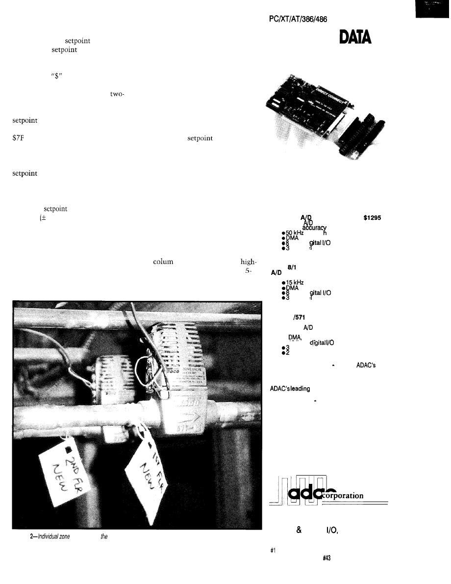
Users!
“00” then no change is made to the
low temperature
or the high
temperature
held within the
DS1620. Nonetheless, a network
response is formulated. The response
consists of a
character followed by
two ASCII checksum characters, a
space followed by a “T,” then a
digit address, a two-digit actual
temperature value, a two-digit mean
value, a single ASCII span
digit, and carriage return. It looks like:
T0054524.
The central control system can
poll each thermostat, optionally
setting a new mean temperature
(turning up or down the
thermostat). Each thermostat will in
turn update the central controller with
the present temperature (Celsius
l
2),
the present
(Celsius
l
2), and
the span degrees about the setpoint).
Although each thermostat has the
ability to directly control the furnace/
zones, you may choose to have the
central controller do this (assuming it
is installed near the furnace). The
central system can accomplish this
through mechanical or solid-state
relays driven by the controller. This
can reduce the number of wires to
each thermostat, however it elimi-
nates the ability of each thermostat to
call for heat in the event of central
controller failure.
The communication routine has
priority over the main loop. However,
if either of the push buttons is being
pressed at the thermostat, communica-
tion is ignored while the user makes
local temperature adjustments. This
assures only one source can make
changes to the
at any time.
SELF HEATING
The circuitry must be as low
power as possible to avoid heating up
the area where we are trying to
measure temperature. The largest
radiator of heat would be a simple
linear power supply. Since we are
starting with 12 volts and only using 5
volts on th board, 7 volts is being
wasted across the regulator. To
eliminate that kind of heat dissipation,
I dug out the MAX638 I used back in
my
for issue 38. This is a
efficiency DC-DC converter with
volt regulator. In that article, I used it
to make the best use of all the energy
Photo
valves control flow of hot wafer to the area of the house requesting heat.
16 BIT
ACQUISITION?
Don’t Settle For Less
Than The Cutting Edge...
HIGH PERFORMANCE
Guaranteed 16 bit accuracy
6 Channel
Board
l
16 bit
resolution
l
16 bit
throug put
lines di
channe
counter/timer
LOW COST
16 bit
6 Channel
Board
l
16 bit ND resolution
throughput
lines di
channe
counter/timer
$895
OPTIMUM CONVERSION’”
DT2601
6 compatible
ND Board
l
16 bit
resolution
l
16 bit accuracy
l
Prog. Gain
l
16 lines
channel counter/timer
D/A channels
$1395
Cut
through the specs each of
16
bit boards have been evaluated against
every competing model. On noise
performance, speed, ease of use, and price,
technology wins every time.
See for yourself Call for an evaluation
board today.
I - 8 0 0 - 6 4 8 - 6 5 8 9
We’ve been making data
acquisition boards for longer
than anyone in the world.
70 Tower Office Park, Woburn, MA 01801
FAX (617) 938-6553 TEL (617) 935-6668
Analog Digital
Industrial PCs,
and High Channel Count Systems
28
The Computer Applications Journal
Issue
February 1994
61
packed inside a
battery. Here I
want to use it for its efficiency as a
volt converter/regulator.
The MAX638 is supplied through
a series diode to prevent damage from
an inadvertent power reversal. All
logic devices in the circuit are HC type
to further reduce heat. The
RS-485 terminator draws more current
(50
than the rest of the circuitry
put together (although it is supplied
only by the active transmitter).
ELIMINATING THE MERCURY
The familiar glass tube filled with
silver fluid may bring back visions of
your childhood. Remember when
Mom placed the cool stick beneath
your tongue to verify your justification
for not going to school? Or, seeing the
liquid blob roll back and forth to make
and break an electrical circuit. These
items are slowly finding their way into
antique and curiosity shops.
Managing furnace relays and zone
valves can require controlling
voltage AC with operating currents in
excess of 1 amp. Most small DIP relays
won’t handle the continual abuse of
these switching inductive loads. I use a
optoisolated triac when control
from the local thermostat is required.
The
thermostatic output
will directly drive the solid-state
relay’s internal LED. The isolated triac
switch can directly drive those control
relays and provide isolation between
the furnace and central controller.
SIMPLE (CENTRAL CONTROL)
SETBACK SOFTWARE
Setback control can be as simple
or complex as you desire. The simplest
control consists of turning the thermo-
stat
down every evening after
retiring for the night and up prior to
rising each morning.
I wrote a BASIC-52 program to
communicate with eight thermostats.
There are two problems with
52 for this purpose. The first is that
processor bit TO, which enables the
RS-485 driver, is not accessible
through any BASIC command. A CALL
can be used to access a pair of
instruction assembly language
tines. The first two, C
LR TO
and
RET,
place the 75176
transmitter/
receiver) into receive mode. The
second two,
TO
and RET, place
the 75 176 into transmit mode. It turns
out not to be such a big deal.
The second problem is much more
difficult. The BASIC-52 I N P U T
statement must be terminated by a
carriage return. If for some reason a
reply is not received from a polled
thermostat, the system will wait
indefinitely. It is true that I could have
used a watchdog circuit to whack the
reset line if this happened, but the
program would only lock up again next
time the thermostat did not respond.
The solution I chose was to use
Systronix’s BCI-51 BASIC compiler.
These guys understood the limitation
of BASIC-52 when they designed their
803 1 integer compiler. The compiled
I N PUT routine can be interrupted by
either
or
The second
function, 0 NT I ME, will interrupt the
I N PUT routine after x amount of time
has passed. Since the RS-485 receiver
can be always enabled on the RTC52,
The Computer Applications Journal
will occasionally provide a listing of
subscribers to vendors with offers of
substantial interest to our readers.
If you would prefer not to be part of
this listing, send the mailing label from
the outside cover of the Computer
Applications Journal along with your
request to:
THE COMPUTER
APPLICATIONS JOURNAL
SUBSCRIBER SERVICE DEPARTMENT
P.O. BOX 7694
RIVERTON, NJ 08077
J
62
Issue
February 1994
The Computer Applications Journal
l
2 Year Warranty
Support by phone
30 day Money Back Guarantee
l
FREE software upgrades available via BBS
l
l
2716 8
16
l
Flash
(EMP-20 only))
l
Micros
l
GAL, PLO from NS,
NEEDHAM'S
Orange Grove Ave
Sacramento, CA 95841
(Monday-Friday.
8 am-5
PST)
C.O.D.
BBS
(916) 972-8042
FAX (916) 972-9960
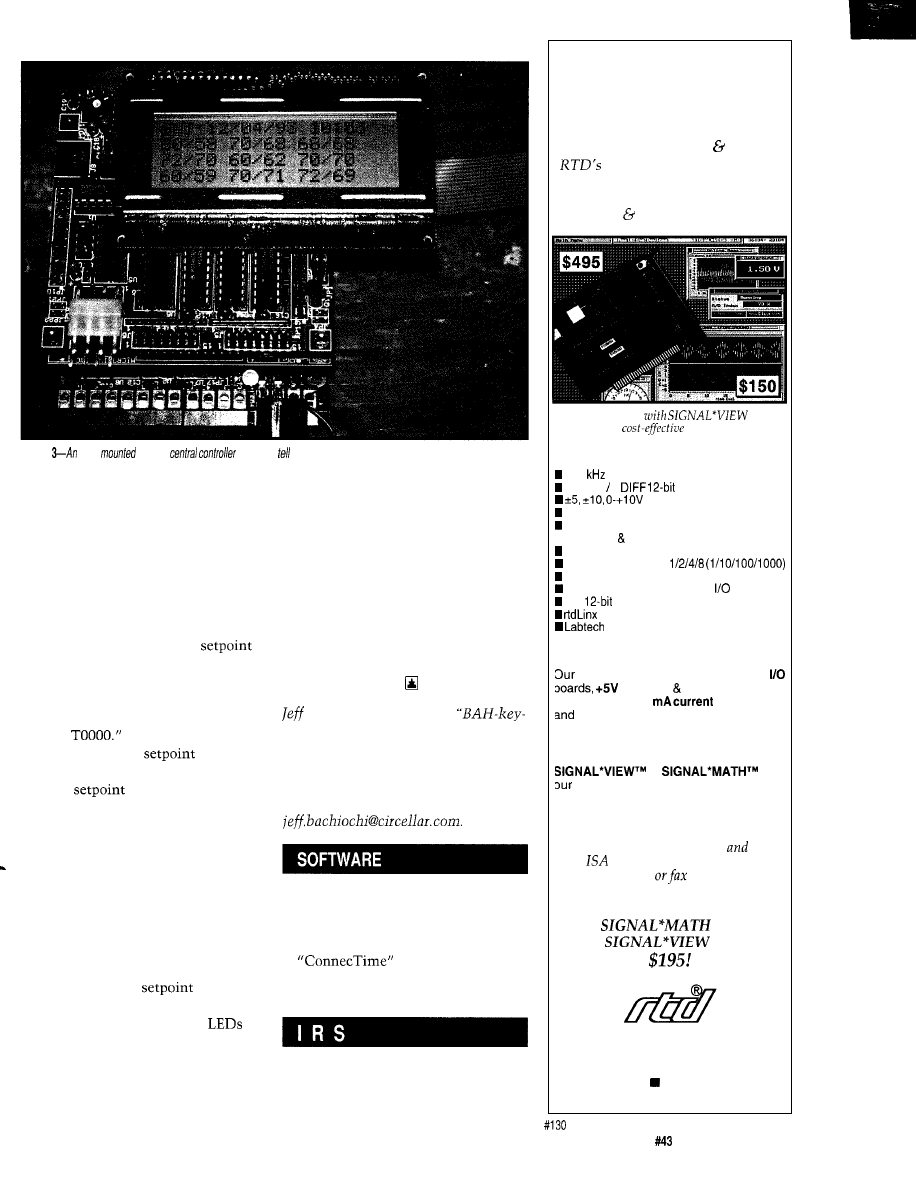
Photo
LCD
on the
lets you at
a
glance the status of each thermostat
the 0 NT
I M E
interrupt routine can send
out a carriage return which will be
heard by itself and complete the
I N P UT
statement. If the
I N PUT
string contains
only a carriage return, the thermostat
is flagged as not responding.
The structure of this program is
simple. First, it reads the “time of day”
and “day of week” from a clock/
calendar. Next it assigns the
times and temperatures from the
user’s list based on the day of week.
Now it prepares to poll the first
thermostat by building a string equal
to “#00
If the present time
matches any of the
times, it
replaces the last two characters with
the new
temperature value.
The program adds up all the character
values to derive a one-byte checksum
(ignoring overflow). Next, it replaces
the two “00” checksum digits with
two ASCII digits equal to the two’s
complement of the checksum. Finally,
it enables the RS-485 driver, sends out
the string, and disables the driver.
The thermostat’s return message
will indicate the present temperature. I
display the present
and the
actual temperature (or “no response”)
if an LCD display is attached.
driven off port
1
indicate where in the
polling sequence the program is.
After each thermostat has been
polled, the loop returns, the clock/
calendar is read again, and the whole
cycle completes.
Remote access to the central
control system could be added to give
you telephone access to any or all
thermostats from the office, airport, or
your car. If you’re thinking that the
HCS II might make a good central
controller and would like to see the
thermostat supported by XPRESS,
please give us your input. Until next
month, stay warm.
Bachiochi (pronounced
AH-key”) is an electrical engineer on
the Computer Applications Journal’s
engineering
staff.
His background
includes product design and manufac-
turing. He may be reached at
Software for this article is avail-
able from the Circuit Cellar BBS
and on Software On Disk for this
issue. Please see the end of
in this issue for
downloading and ordering
information.
416 Very Useful
417 Moderately Useful
418 Not Useful
Data Acquisition
and Control
Without Compromise
Programmable Scan Burst
Advanced Industrial Control
boards set a new performance
standard for general purpose
industrial laboratory applications.
ADA2210
A
solution
ADA221 0 features:
125
XT throughput
16 S.E. 8
analog inputs
selectable input range
programmable auto channel scan
programmable burst mode
n software external triggers, pacer clock
on-demand DMA transfer
programmable gain:
3 cascadable 1 B-bit counters
lines
two
analog outputs, selectable range
Universal TSR DOS driver
N o t e b o o k d r i v e r
HARDWARE SOLUTIONS
AIC family also includes AT
only A/D control boards for
sortable PCs, 4-20
loop outputs,
opto-22 compatibility.
SOFTWARE SOLUTIONS
Select the power and performance of
or
from
library of application programs for moni-
toring, data acquisition and analysis, control,
DSP and 3D graphics.
For more information on these
other
bus and PC/l 04 products,
call, write
us today!
Place your order now and receive
and
for
Real Time Devices, Inc.
P.O.
Box 906
State College, PA 16804
(814) 234-8087 Fax: (814) 234-5218
The Computer Applications Journal
Issue
February 1994
6 3
Op-amp
Terminators
Tom
output frequency is
explanation can be offered for this
difference.. This handy little quote
can be found in “Design of Op-Amp
Circuits,” on page 141, Howard M.
Berlin, ISBN O-672-21537-3. Hey
Howard, the explanation is
FIRST you stir the entrails, THEN you
throw the sticks.
Well-known to be a
kind
of guy, it’s not surprising that analog
stuff is an occult art to me. The fact
that it’s also a mystery to the experts
is even more interesting.
Sure it would be nice if 1
were enough, but the “real
including our own five sensory
channels-is undeniably analog.
Maybe someday we’ll all have “slots”
in our forehead, but until then the
follies and foibles of analog circuits
have to be dealt with.
While I confess to an intellectual
curiosity about all this, sometimes
(i.e., when the bills are due) I’d rather
get something working than explain
why it doesn’t. Fortunately, as
discovered at a recent Burr-Brown
seminar, traditional op-amp suppliers
are supplementing their lines with
“solution-oriented” parts that take
much of the voodoo out of analog
design.
I SEE THE LIGHT
A classic (indeed, it’s the same as
Figure 4-3 in Berlin’s book) op-amp
circuit converts the variable current
passing through a photodiode to a
corresponding voltage using an
amp. Unfortunately, in the words of
Burr-Brown’s experts, it’s a solution
that’s ..often destined for failure...”
as shown in Figure
It is interesting to note that you’ll
find op-amp books, data sheets,
seminars, and so forth sprinkled with
words like
often, might, should,
and
even
hope.
Welcome to the world of
analog design.
According to the experts, the
explanation is
simply, the
open-loop curve of the amplifier and
the noise gain curve of the feedback
network have a greater than
decade difference in their slopes at the
intersection.” For those of you who
think this explanation isn’t “quite
simple” enough, the translation is
simply “hang a cap on it” (see Figure
Oops, now the bandwidth is all
shot to heck. Peering into the crystal
ball-yes, I see a faster op-amp in your
future. That should do it,
So
sorry-the new op-amp is faster all
right but the signal-to-noise ratio is
still poor. Fortune cookie says, “Stay
out of debt, use a low-noise
Surely this will solve the problem,
right!
But nooo, turns out the input
capacitance of the new op-amp is
different enough to goof everything up,
making the noise worse.
On and on they went, with at least
a dozen slides contemplating the
thermal noise of resistors, femptoamps
per root Hertz of current noise, and
other mysteries of the cosmos.
Photo
integrates
the photodiode, amp,
and
on a
die in a clear plastic package.
64
Issue
February 1994
The Computer Applications Journal
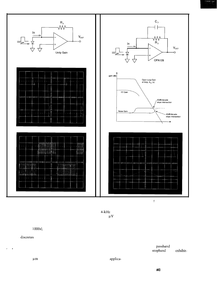
Stable Amplifier
Figure 1-A
simple current-to-voltage converter circuit looks good in theory, but in
practice fails terribly in response to a pulse input.
log f (Hz)
Figure
2-Adding a capacitor to the circuit in Figure cleans up the garbage, but
drastically reduces the bandwidth of the circuit
I was beginning to fear nothing
short of human sacrifice would make
the darn thing work. Fortunately,
bloodshed can be avoided by using the
OPT201 ($4.35 in
a device that
uniquely integrates the photodiode,
amp, and
on a single die
exploiting the “why didn’t I think of
that” concept of using clear plastic
is specified to achieve
band-
width with a minuscule 30
of
noise.
FILTER PRAYERS ANSWERED
Another common op-amp applica-
tion is to filter signals, passing only
frequencies higher than, lower than,
or in between the desired cutoffs.
tions, with separate high-pass (VHP),
low-pass (VLP), and band-pass (VBP)
outputs. In actual practice, a particu-
lar setup is usually optimized for
either high- and low-pass (and by
combining them, notch) or band-pass
response.
An immaculate filter would pass
everything in the
and
for the package (Photo 1 and Figure 3).
Figure 4 (Berlin figure 7-7) shows a
nothing in the
while
The OPT201 is most sensitive to
universal active (a.k.a., state variable)
infrared light (770
wavelength) and
ing no noise, ripple, or ringing to boot.
filter that serves a trinity of
Earthly filters, doomed to sin, make
The Computer Applications Journal
Issue
February 1994
6 5
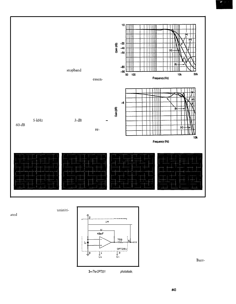
FILTER GOSPEL ACCORDING TO...
Butterworth: Very flat magnitude response (i.e., gain is
0
constant throughout the passband) with fairly steep
-10
cutoff (i.e., attenuation in the stopband). Impulse
-20
response has moderate overshoot and ringing.
Chebyshev: Achieves better cutoff than Butterworth at
the expense of some ripple (gain variance) in the
passband. Impulse response shows a lot of overshoot
-60
and ringing.
-70
Inverse Chebyshev: Improves on the Chebyshev by
moving the ripple into the
and cleaning up
the impulse response.
lk
Bessel: Achieves the best impulse response with
tially no overshoot or ringing. For a given filter
complexity, the magnitude and cutoff response lags
3
Butterworth, but this can be overcome by adding
0
poles. If you’re willing to pay the price, a high-order
-3
Bessel filter is the way to go.
-9
-12
Both figures to the right show gain versus frequency for
fifth-order
[a) Butterworth, (b)
Chebyshev, (c)
Inverse Chebyshev, and (d) Bessel unity-gain low-
pass filters. The top figure shows the overall filter
sponse with the bottom figure shows the transition-band
detail. Below are step responses for the same four filter
configurations (a-d, left to right).
-15
-18
-21
-24
-27
loo
lk
various tradeoffs between the criteria.
Analog sinners can be saved with
So, the first challenge for the
the UAF42 ($6.40 in 1000s) which
is to learn the teachings of the
combines four op-amps with precision
various disciples-Butterworth,
discretes to support a variety (type,
Chebyshev, Bessel, and so on (see the
‘4
number of poles, etc.) of filter designs.
sidebar)-that testify to a particular
,
Simple filters require only a single
filter’s fallibility.
UAF42 and two external resistors.
Given our previous experience
More sophisticated (i.e., using more
with the simple photodiode amp, it
poles) designs are possible using
would be miraculous indeed to get the
multiple UAF42 chips and perhaps an
more complicated filter working.
extra capacitor or two-far fewer
Ultimately, a cursed designer might
discretes (and potential trouble spots)
just frantically add more op-amps,
than a traditional op-amp design.
resistors, and capacitors in a quick
Brown also provides
F
I LT E R4 2,
a
attempt to clean up the mess, ending
Figure
integrates the
DOS-compatible program which
up with an expensive white noise
amp,
and discretes on a sing/e die using a clear plastic
makes designing a particular filter
generator.
package.
quite easy.
The Computer Applications Journal
Issue
February 1994
6 7
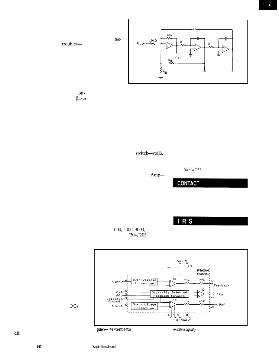
Remember, finally getting a
traditional analog circuit working is
only half the battle. Keeping it work-
ing is another story considering the
veritable witch’s brew of
sloppy component tolerances, thermal
drift, and dubious wiring-that can
crop up in production. Your finely
tweaked design may go south with the
next batch of caps. It’s little consola-
tion, but being unemployed will give
you plenty of time to explain what
went wrong. By contrast, the UAF42
design is blessed with predictable
chip layout and wiring and tight
trimmed) 0.5% tolerance RC net-
works.
GAIN WITHOUT PAIN
I’m sure the Puritans would rail
against such newfangled “easy-to-use”
parts. Given we’re put on this mortal
coil to suffer, it’s hard to imagine a
more fitting penance than being
chained to a balky op-amp design.
Besides building character, it makes
that inevitable trip to the hereafter
start to seem like something to relish,
rather than fear.
If we weren’t meant to suffer, how
come no real-world sensor puts out the
O-5 V a typical A/D converter de-
mands? Interfacing any particular
gadget typically requires a special [and
expensive) signal conditioner to make
the match. Enter the instrumentation
amp (IA) which differs from an op-amp
in a few key ways.
First, the IA features high com-
mon mode rejection (CMR) and thus
can dampen noise present on both
inputs. For example, connecting a
ground-referenced signal to one input
and ground to the other can eliminate
ground noise of either the periodic
(i.e., 60 Hz) or the transient variety.
This helps deal with the reality that
sensors are usually at the end of noisy
cables.
Secondly, an IA includes built-in
precision feedback components which,
as we’ve seen, eliminates the potential
trouble posed by the external
of a
regular op-amp design. The previously
mentioned CMR also benefits from
precision, since even
1%
resistance
tolerances can shrink it to a scant 46
Figure
4-A universal
active
filter
provides
the designer with
separate
high-pass,
low-pass, and
pass outputs.
1 0 k
C
C
“ B P
“ L P
Finally, the inputs of an IA are
buffered, presenting a quiet, stable,
high-impedance input to the sensor.
Note that in an unbuffered op-amp
design, the input impedance is low and
varies depending on the gain which
may negatively impact bandwidth for
weak signal sources.
With gain set by a single resistor
that has no deleterious effect on the
input, one trick is to hang multiple
resistors on an analog
you now have an IA with program-
mable gain.
Better yet, choose a PGA204 or
PGA205 (Programmable Gain
$6.50 in 1000s) which includes the
digitally selected gain resistors on chip
(Figure 5). The ‘204 features gain
selections of
1, 10,
100, and 1000 while
the ‘205 offers gains of 1, 2, 4, and 8.
You can cascade multiple units for
more range-for example, a ‘204 and a
‘205 in series expands gain selections
to 1, 2, 4, 8, 10, 20, 40, 80, 100, 200,
chip’s power supply, so you don’t need
to worry about a software error
(choosing too much gain) feeding 8000
V to your A/D converter. Furthermore,
the inputs are protected up to 40 V, a
feature that not only adds robustness
but can eliminate the need for extra
i n p u t l i m i t c i r c u i t s .
q
Tom Cantrell has been an engineer in
Silicon Valley for more than ten years
working on chip, board and systems
design and marketing. He can be
reached at (510) 657-0264 or by fax at
(510)
Burr-Brown Corporation
P.O.B.
11400
Tucson, AZ 85734
(602)
746-1111
400, 800,
and 8000.
419
Very Useful
A plus for the
chips is
420 Moderately Useful
that the output limit is dictated by the
421
Not Useful
U o s
provide the ultimate in flexibility
selectable gains, and a/so offer low
noise and high common mode rejection
68
Issue
February
1994
The Computer
Data
Logging and
Collection
Devices
John Dybowski
controllers come in
only natural since the applications
they are pressed to serve are equally
diverse. Among the many applications
for embedded controllers are appliance
control, medical instrumentation,
down-hole monitoring, and
powered weather surveillance systems.
Looking at embedded controllers
from another perspective, the differen-
tiating features are often perceived to
revolve around the controller’s
underlying technology and architec-
ture rather than its eventual usage.
These days, 32-bit controllers are
becoming commonplace in applica-
tions that were simply not possible
before their arrival.
Of course, this is not to say that
their smaller
and
siblings are faced with extinction.
Designers of embedded systems are a
practical lot, and many, if not most,
embedded systems can be served
perfectly well using
controllers.
After all, if all you need is a
transistor, then that’s what you will
use. Similarly, you may find that an
8051 has all the horsepower needed for
a given application. Why fight it?
I’VE FALLEN AND I CAN’T GET UP
The balance of power has actually
come full circle if you consider that
parts like the 8051 still prevail in
many new embedded designs. Evi-
dently, those who proclaimed the
death of S-bit
were, shall we say,
a bit premature. What’s surprising is
not so much the fact that the
8051 is
15 years old, but that new derivatives
based on this basic architecture are
still being introduced on a regular
basis. Many of these newer 805
1
derivatives contain additional built-in
features. As a result, some of these
parts can get pretty expensive. The
important thing here is that this
architecture is familiar to many
engineers and the tools are in place to
expeditiously turn designs around.
Maybe you started using the 8051
because you needed a $2 controller,
but the situation is a bit different now.
Evidently though, once you’ve taken
the plunge, it’s hard to go back.
It should be apparent that some
problems require the aid of a high-
tech,
or
powerhouse to bring
them into check. It is equally clear
that many applications can be put to
rest by applying relatively low-tech
solutions. The median is, of course,
the domain of mid-tech computing
devices, which is the place between
the perils of the leading edge and the
trailing mundane. This is a comforting
thought for many engineers since this
middle ground is a relatively safe
place. It is founded on familiar and
stable technology, yet still possesses
the potency to manage many challeng-
ing design problems.
I should back up now and touch
on some common functions that are
useful in a variety of control tasks.
These function blocks form the basis
of many general-purpose embedded
computers. Also, it would be wise to
temper this discussion with the
knowledge of what constitutes modern
design practices and how these impact
the fundamental embedded computer
requirements.
The basic requirements of a
general-purpose embedded computer
would include the following items:
*Real-time clock/calendar
*Digital I/O
*Analog I/O
*Nonvolatile RAM
l
RS-232 or RS-485 serial ports
l
E2PROM for parameter and setup
information
expansion capabilities
In addition, the following elements
could be used in certain applications:
70
Issue
February 1994
The Computer Applications Journal
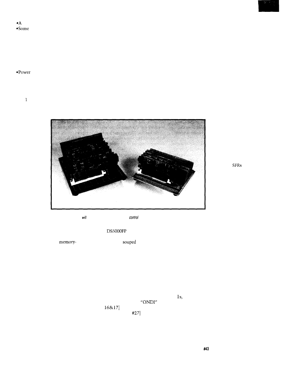
display and keyboard
sort of mass storage system
*A watchdog timer
*The capacity for battery operation
And for those applications that relied
on extended battery life:
*All-CMOS design
management
*Battery management
amazed that these same people would
not hesitate spending an equal amount
of money on some lame single-board
computer that offers only a fraction of
the functionality of these highly
integrated controllers. It’s a curious
state of affairs, and I suppose it all
boils down to a matter of perception.
Some folks take an 803
1,
an address
latch, and an EPROM and call it high
tech. Most of us know better.
THE NATIVE 8031
In spite of all the peculiarities of
the 803 architecture, I’ve always been
impressed with its bit manipulation
capabilities. This appreciation came
after my initial
horror of its
twisted little
architecture
faded. In contrast
to the rigors of
accessing the
805 l’s external
data space,
manipulating the
bit-addressable
port pins is
relatively
straightforward.
Sadly, most
implementations
that use the 803 1
in expanded mode
sacrifice many of
the I/O pins to
Now that I’ve stated why I think
these Dallas controllers have the
characteristics on which to base a
general-purpose embedded computer
system, let me briefly recap what these
parts bring to the party. First off, the
of available memory supported, both
parts are functionally equivalent. Since
the built-in RAM is accessed via
internal data, address, and control
buses, this leaves all of the on-chip
ports available for use as general I/O.
Finally, we have a platform that allows
us to have memory and I/O at the
same time! Besides all this, the
lithium-based RAM can be partitioned
as either program memory or data
memory, which allows using this
memory in the most efficient manner
for the particular application. This
partitioning can be performed either
during initial program loading or
dynamically under
Photo l-Although the
chief purpose of this embedded computer is for data collection and data logging,
experienced engineers find this system useful for other
system applications.
firmware control in
reasonably small
increments.
Additional
features such as a
built-in watchdog
and power-on
reset, power-fail
interrupt, and
additional
specialized
provide function-
ality that is quite
useful in many
embedded
computer
applications. An
integral bootstrap
loader allows
serial or parallel
program loading,
their alternate functions as the data
bus, address bus, and other memory
control functions. As a result, you
frequently end up adding
mapped I/O, which leads you back to
the rigors of accessing the 803
l’s
external address space. I’m sure you
appreciate the nature of the problem.
Those of you who have followed
my columns may recall that, on
occasion, I’ve managed to circumnavi-
gate this problem using controllers
such as the DS5000 and DS2250 from
Dallas Semiconductor. Essentially
possessing the fundamental elements
of some of the single-board computers
on the market, these controllers
provide an ideal foundation on which
to build a compact and flexible
embedded computer. Some complain
these parts are overpriced, but I’m
DS5000 and DS2250 are both based on
a Dallas
processor core
which, for all intents and purposes,
looks a lot like a
up 803
1.
The
DS5000 encapsulates this core proces-
sor along with up to 32K of RAM, an
optional real-time clock, and a lithium
backup power source (rated at ten
years) within a 40-pin DIP package
that maintains pin and function
compatibility with a standard 803 1.
The DS2250 provides the same
functionality along with a maximum
of 64K RAM on a less-expensive 40-pin
SIM affair. (Check out my
[issues and “The Elements of
a Data Logger” [issue
articles for
additional insight into the inner
workings of the DS5000 and DS2250.)
Other than the differences in
packaging and the maximum amount
memory partitioning, program verifica-
tion, and setting various chip configu-
ration options from your PC. This
capability essentially eliminates the
need for EPROM emulators that are
frequently used during initial program
development. It turns out this feature
can be put to good use when develop-
ing programs that will run on parts
that don’t support any external
program memory at all. For example,
when I was toying with an 8751
project a while back, rather than burn
875 I just used a DS5000 and
downloaded the code until I got it
right. Once I knew it worked, I then
burned my 875 l-once.
WORK THOSE BITS
Using the DS2250 with all of
those easy-to-use I/O bits lets you
The Computer Applications Journal
Issue
February 1994
7 1
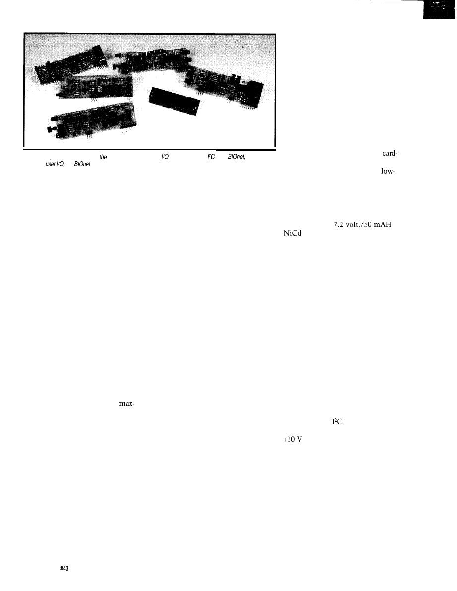
Photo 2-System elements include processor board,
power power manager, core,
battery
manager,
and
satellite.’
proceed in two different ways. If what
you’re doing is developing a controller
to satisfy some specific purpose, and
you’re putting it together from the
ground up, then your course is pretty
well charted.
On the other hand, if what you’re
doing is developing a general-purpose
embedded computer, then it’s impos-
sible to anticipate what burdens may
ultimately be placed on the instru-
ment. Naturally, you have to provide
some basic feature set while leaving
room for future expansion. At the
same time, it’s advisable to limit your
focus and set some reasonable limits
on the device’s eventual capabilities. If
you try too hard to design an embed-
ded computer that is all things to all
people, you may find yourself the
hapless creator of something that is
ultimately nothing to everybody.
You’ve got to walk the line.
Assuming you’ve set your sights
properly, it makes sense to subscribe
to the old engineering adage of
for-min. The key is to not paint
yourself into a corner and also to
provide a reasonable amount of
flexibility without getting carried
away. Developers of embedded
computers have traditionally coun-
tered this quandary by providing some
sort of bus architecture in order to
furnish an avenue for handling options
as needs arise.
This is a reasonable idea, but it is
not entirely without problems. By its
very nature, such an architecture
usually involves numerous connec-
tions to carry the processor data and
address bus as well as the required
control signals. To support signaling
across multiple boards, buffers,
decoders, and the various byte-wide
memory and I/O components all add
to the burden. This approach is not
only costly but raises reliability
concerns because of all those connec-
tors.
An alternate way of dealing with
the expandability issue is to use the
on-chip I/O bits of the DS2250 as a
sort of uncommitted bus. Since these
bidirectional pins operate completely
under firmware control, ultimate
flexibility can be realized. Each pin can
be dynamically defined as input,
output, or bidirectional. The timing of
each pin can also be controlled to suit
the individual peripheral function it is
assigned to control. Since these
functions operate under firmware
control, a modest level of throughput
is implied. But remember that the
DS2250 controller is self contained
and runs at the full bus bandwidth. If
this all sounds a bit familiar, then
you’ve been following my recent
columns where I’ve demonstrated how
to control a multitude of functions
serially with a basic 803 1. Admittedly
I’ve approached this subject piecemeal
and somewhat unevenly thus far, but
now I’m ready to come clean and show
you how to put it all together.
A COMPACT EMBEDDED DATA
COLLECTION COMPUTER
I’d like to take a little time to
describe the basic system configura-
tion for a general-purpose data collec-
tion computer so we can operate from
a common baseline.
This embedded computer is
centered around a DS2250 controller
with 64K of battery-backed memory
and running at 11.0592 MHz. The
computer is based on a carrier card
(something of a backplane) that holds
the DS2250 and all of the feature
cards. The feature cards sit vertically
atop the carrier and allows the system
to have a very small footprint. A 3%
conductor bus is defined to consist of
24 general-purpose I/O bits, a couple of
dedicated control bits, a number of
power connections, and several
to-card control signals.
The system is designed for
power operation. The basic configura-
tion is capable of running from line
power, or off a battery for an extended
period of time. In order to supply
power to the various feature cards, a
relatively hefty
battery is specified. This battery
should suffice for most applications.
But depending on which features you
want to use and how you want to use
them, many applications could work
perfectly well with a much smaller
battery.
Although intended for general use,
this embedded computer is ideally
suited for data collection and data
logging. Photo 1 shows a typical
system configuration. Also presented
in this photograph is my initial
handwired prototype that served as the
test bed for my development. In Photo
2, the system is dismembered so you
can see the cards that comprise the
system. As I briefly describe each card,
see if you can pick it out of the lineup.
The Power I/O card provides a
line-powered RS-232 port, a CMOS
RS-485 port, an
port, and a line
power connector. Also on this card is a
regulator that preregulates the
line power to a level that the
micropower switch-mode regulators
(that reside on the other cards) find
palatable. Finally, a couple of jumpers
are provided to support the system
bootstrap loader. These jumpers allow
you to control bootstrap mode. You
can set the jumpers so that the
bootstrap load can be invoked via the
Loader Utility from the host PC, or
you can completely inhibit this
capability, or you can invoke it
7 2
Issue
February 1994
The Computer Applications Journal
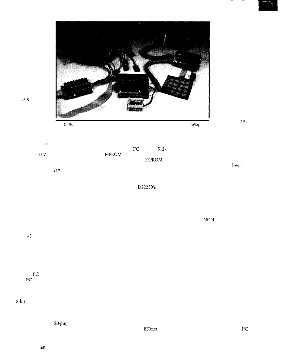
Photo
complete system includes
processor
board, interfaces, displays,
keypad, sensors, and
power
management.
manually.
The
LED on this card
signifies that
bootstrap mode is
in effect when it
is lit.
The Power
Manager contains
two voltage
regulators for the
system. One of
them is a
micropower pass
regulator running
at
V that
sources backup
power for
nonvolatile
peripherals, and
the second one is
a micropower
switch-mode buck regulator for
supplying the V used to power the
system’s logic. If you were wondering
about the
preregulator, it is
there because the buck regulator used
in this design tends to self-destruct if
hit with more than
V.
This card also contains control
logic that serves to control the +5-V
logic regulator. This logic turns on the
system power in response to the
application of line power, a pulse on
the manual push-button switch, or via
a signal generated by one of the other
feature cards. Shutdown is accom-
plished by the system processor via a
port pin. The LED indicates the
system is active and is on when the
main V is present. An output is
provided to the system processor that
indicates that the system is operating
under battery power. Another output
signals when the battery is failing and
warns that the main +5-V switcher is
about to lose regulation.
The
core contains all of the
local
peripheral functions and
provides the majority of the system
I/O. Contained here are 8 bits of
bidirectional digital I/O, 8 channels of
A/D conversion, and 2 channels
of 8-bit D/A conversion. The analog
section operates at levels of 0 to 2.5 V.
All of the digital and analog I/O signals
are brought out to a
double-row
header. Channel 0 of the ADC is
configured to monitor the battery and
allows the processor to monitor the
battery’s discharge progress.
Also riding the
bus are a
byte
and a real-time clock.
You may wonder why the
would be included in this configura-
tion since the DS2250 already has a
significant amount of nonvolatile
RAM. The answer to this question is
that everything in the
memory is lost when you use the
bootstrap loader to download programs
to the system. In this case, it’s benefi-
cial to have a separate holding area for
configuration, setup, and identification
information.
The RTC is not only the time-
keeper for the system, but also
generates the enable signal that is
ultimately routed to the power control
logic and is used to bring the system to
life. This RTC alarm function is very
flexible and the signal can be pro-
grammed to fire off on a specific date
and time, or it can be configured to
operate as an interval timer with
increments anywhere from a fraction
of a second to a number of days. This
alarm output is buffered and presented
to the system processor and can be
polled or used as an interrupt source.
Finally, the RTC contains 256 bytes of
nonvolatile RAM that can be used for
additional miscellaneous storage.
Extended digital sense and control
points are handled by the
card.
On occasion, there is a need to
monitor and
control digital
points that are
dispersed over a
wide area.
Usually this must
be handled by
bringing numer-
ous cable bundles
back to the
central controller.
This card, along
with its associ-
ated satellite
peripherals,
alleviates this
problem. Con-
taining a
micropower +
V switch-mode
boost regulator
and related interface circuitry, up to 60
inputs and 60 outputs can be serviced
over a single twisted-pair cable. The
interface allows driving the data and
power over these two leads. This
configuration is optimized for
power operation and allows moderate
line lengths from 250 to 500 feet. The
on-card LED indicates when the
network is active.
Since the system is fully capable
of operating from battery power for
extended periods, it makes sense to
show some kindness to the battery.
The battery manager is configured for
fast charging a
battery using
constant current. Primary charge
termination is achieved using the
negative delta voltage method and
requires no temperature sensors. For
safety, charge is unconditionally
terminated following a maximum time
period should the primary cut-off
mechanism fail.
For battery conditioning, and to
ward off the feared memory effect,
discharge-before-charge can be initi-
ated by activating a manual push-
button switch. The LED indicates
various charge functions via different
sequences of on/off patterns.
User I/O is important, and this
embedded computer allows some
flexibility in this regard. The LCD/
keyboard interface is an PC-based
component that can connect to the
port of the Power I/O card if you want
74
Issue
February 1994
The Computer Applications Journal
to operate this section remote to the
controller. The interface card con-
sumes two
addresses when the
keyboard is included and only one if
just the LCD is used. In any case, a
number of free addresses are available
so this is not a problem. This card is
the same size as a typical 20x4 LCD
and attaches discreetly beneath the
display panel. A
digital port is
provided that allows connecting a
beeper and other extra devices such as
The
bus is carried through
to a second connector to allow daisy
chaining additional devices if neces-
sary. The complete system shown in
Photo 3 uses this feature to handle a
fully independent secondary LCD.
Even if your end product does not need
such capabilities, it is quite a useful
feature to have during system debug-
ging.
Now that I’ve described the cards
that comprise the basic system, let me
summarize each card individually. Just
so we can keep score, I’ll also note the
number of I/O pins each card con-
sumes.
POWER
@Line-powered RS-232 port
*CMOS RS-485 port
*Host control of bootstrap loader
(with jumper defeat)
*Manual control of bootstrap loader
port for
keyboards, and
other peripherals
l
+lO-volt preregulator for
micropower switchers
pins used: 3 for SIO
port
uses same 2 pins as
core)
POWER MANAGER:
l
+Svolt
micropower switch-mode
buck regulator
l
+3.5-volt micropower
mode regulator for backup
power
*Battery/line signal
*Battery fail signal
*Power control logic turn-on via:
Programmable RTC/timer
Manual push button
Attachment of line power
*Power control logic shutdown
under processor control
pins used: 3
CORE:
channels of 8-bit ADC with an
input range of O-2.5 V
*Battery monitoring via ADC
channel 0
channels of
DAC with an
output range of O-2.5 V
*Real-time clock/calendar
12 byte
bytes of RAM
bidirectional digital I/O lines
*Programmable interrupt source
*Programmable RTC/timer wakeup
stimulus
pins used: 2
BIONET:
micropower
switch-mode boost regulator
v
l
BIOnet port for up to 60 remote
I/O points over twisted pair
pins used: 4
BATTERY MANAGER:
*Constant-current source charger
to trickle charge
*Charge termination via negative
We’re
Powerful,
And We’re Cheaper.
MMT-188 EB
2 serial
ports
3 programmable parallel
5
RAM/ROM capable
powerfail detect interrupt
and reset
counter- timers
watch dog timer
expansion connector
ALSO AVAILABLE:
MMT-196,
MMT-EXP
In fact, you’ll get the best product for about
half the price. If you’re interested in getting the
most out of your project, put the most into it.
For the least amount of money.
Call us today’for complete data sheets, CPU
options, prices and availability.
Work
Welcome. Call or fax for
complete data sheets
2308
East Sixth Street
Brookings, SD 57006
Phone
Fax (605)
S
MALL
B
UT
W
E
'
RE
P
O W E R F U L
NEW! UNIVERSAL DALLAS
DEVELOPMENT SYSTEM from
l
It’s a complete single board computer!
One board accommodates any 40 DIP DS5000, 40 SIMM
SIMM
or 72 SIMM DS2251, 8051
processor! Snap one out, snap another in.
l
Programs via PC serial port. Program lock encrypt.
l
LCD interface, keypad decoder, FE.232 serial port, 8-bit
ADC, four 300
relay driver outputs.
l
Power with 5VDC regulated or 6-13 VDC unregulated
l
Large prototyping area, processor pins routed to headers
l
Optional enclosures, keypads,
everything you need
BCl51 Pro BASIC Compiler w/50+ Dallas keywords $399
FAX:801 534.1019
555 South 300
City UT, USA84111
The Computer Applications Journal
Issue
February 1994
7 5
delta voltage method and/or
maximum time
*Discharge-before-charge via
manual push button
pins used: 0 (stand-alone)
These five cards form the funda-
mental peripheral set for the system,
with each card being 1” x in size.
The system carrier contains the
DS2250 and nine peripheral slots. This
card measures 4” x 5”. The configura-
tion 1 described leaves four free slots
open for future expansion. The basic
system accepts the following standard
remote peripheral components:
USER
l
l2C addressable 4x20 LCD
l
l2C addressable 4x4 keypad
*Multiple user l/O cards can be
accommodated by the system
SATELLITE:
input bits
output bits
to 30 addressable satellites
and data over twisted-pair
network that can be up to 300
feet long.
THE EVOLVING CONTROLLER
The embedded computer I’ve
presented is designed to serve experi-
enced engineers as a vehicle for their
specialized data collection and control
applications. In subsequent columns,
will describe in detail both the
electronics and firmware associated
with each peripheral function. I’m
eager to move along and get on with
developing some real applications in
1
order to demonstrate how this embed-
ded computer can be put to use in
various data collection, analysis, and
control tasks.
In order to make short work of
this, 1’11 be doing a lot of the coding in
C, leaving the assembler for the real
low-level stuff. I did mention some-
thing about modern design practices,
didn’t I? With the extra elbow room of
the
64K of memory, this
shouldn’t be a problem at all. The
system’s bootstrap loader will further
serve to expedite the whole operation.
Of course, this is not a static
system, and it will continue to grow
and evolve. After all, that’s the whole
idea. Presently, a memory expansion
card is under development that will
offer 5
of battery-backed SRAM for
more ambitious data collection tasks.
To go hand-in-hand with more
ambitious undertakings, a
analog input card with 0-4.096-V input
span and I2 bits of resolution is in the
planning stages. What’s next? A
smaller battery power option and
perhaps solar power-the embedded
computer goes green.
q
Dybowski is an engineer in-
volved in the design and manufacture
of hardware and software for indus-
trial data collection and communica-
tions equipment. He may be reached
at
422 Very Useful
423 Moderately Useful
424 Not Useful
The BCC52 controller continues to be
Micromint’s best selling single-board com-
puter. Its cost-effective architecture needs
only a power supply and terminal to become
a complete development system or
board solution in an end-use system. The
BCC52 is programmable in BASIC-52, (a
fast, full floating point interpreted BASIC), or
assembly language.
The BCC52 contains five RAM/ROM
sockets, an “intelligent” 27641128 EPROM
programmer, three d-bit parallel ports, an
auto-baud rate detect serial console port, a serial printer port, and much more.
PROCESSOR
B-bit CMOS
detect
Three
printer RS-232
B-bit parallel ports
more!
EXPANDABLE1
BCC52
Controller board
BASIC-52 and RAM
$1 89.00
Single
Low-power CMOS
of the
$199.00
lo
temperature
$294.00
Low-power CMOS, expanded BCC52
RAM
$259.00
CALL FOR OEM PRICING
MICROMINT, INC.
4
Vernon, CT06066
in Canada: (514)
888-6401
Distributor
7 6
Issue
February 1994
The Computer Applications Journal
W
e
a full line of low cost
embedded
controllers and software tools which are ideal for
F e a t u r e s i n c l u d e :
L o w p o w e r C M O S d e s i g n
U p t o 6 0 K o f c o d e s p a c e a n d u p t o 6 0 K o f d a t a s p a c e
5 t o 1 5 v o l t o p e r a t i o n
S m a l l f o r m f a c t o r ( 3 . 5 ” * 6 . 5 ” ) w i t h p r o t o t y p i n g a r e a
Start at $100
Available Options:
M u l t i f u n c t i o n B o a r d a d d s A / D , 2 4 I / O l i n e s a n d m o r e !
BASIC-52 or Monitor/Debugger in EPROM,
C o m p i l e r $ 1 0 0 o r B A S I C C o m p i l e r f o r $ 3 0 0
Iota Systems, Inc.
8 9 8 7
I n c l i n e V i l l a g e , N V 8 9 4 5 2
PH: 702-831-6302 F A X : 7 0 2 8 3 1 - 4 6 2 9
simply as an output annunciator. This month I have
collected eight very recent patents from the 1993 Patent
Database which all deal with applications involving light in
electronics.
The first patent in Abstract is perhaps the simplest. It
uses light reflected from bowling pins to determine which
are standing and which have fallen. A lens focuses the light
onto a linear light sensor array; and (of course) a micropro-
cessor is called into play to extract the information from
this sensor and to communicate the results over a serial
link. Mechanical alignment and proper lighting would seem
crucial to the success of this technique, but it is a novel and
potentially robust and low-cost approach.
The next two patents use the color of a light source, or
of a lighted object, to encode and represent information.
Abstract 2 is a unique and sophisticated imaging system
which makes use of a most simplistic light source. There is
often the need to rapidly measure audience response in a
binary manner [e.g., yes/no). This patent uses colored
reflectors (red on one side and green on the other) which are
held up by the audience to indicate their preference. A
video camera scans the scene and a computer picks out the
red and green “dots” from the background and counts them.
This technique avoids having to wire the seats or provide
selection buttons at each site. It is very simple to use, yet
provides rapid response.
I can envision a number of enhancements. Reflectors
like these found on automobiles and road signs would
return a stronger signal. Using colored flood lights matched
to the objects’ emissivity would enhance the image of the
objects. Increasing the measurement time or doing multiple
counts might account for movement or misalignment. It
would also seem possible to use more than just two colors
where a more complex vote is required, although this would
require more complex (or multiple) signaling objects. While
the accuracy may not be
the system is simple and
fast, and probably quite adequate in many situations.
In contrast, Abstract 3 controls the color of a light
source in order to output data. Using three primary colors
(red, green, and blue, for example), octal digits can be
represented by a color burst containing varying amounts of
these primary colors. A sequence of these signals can be
used to transmit the information on a TV signal, or perhaps
over a fiber-optic or other kind of optical link. The three
primary color constituents are individually filtered and
measured at the receiving end of the optical link. While
attenuation of the signals might vary depending on wave-
length in a direct optical link, the determination of simple
on/off levels would seem to be quite robust. Extension to
more than just eight composite colors would seem possible,
although that method is not presented in the current
patent. With the advent of tricolor
this scheme is
intriguing for many applications.
Somewhat more conventional, it is possible to
amplitude modulate a light source to encode information.
Abstract 4 uses the light source to provide data and power
to a cluster of low-power receiving devices placed within
view of the source. An example is discussed where this
system is used to present information on remote LCD
displays. But remote control of all sorts is also possible.
The ability of light to couple across physical barriers
while maintaining sealing is used by Motorola in Abstract
In this case, the unique barrier is a plastic battery
compartment which contains corrosive fluids. The optical
window also serves as a gas vent for the battery. One would
expect that such a link might measure and communicate
Patent Number
Issue Date
1992 05 19
Inventor(s)
Ross 0
State/Country
AUX
US References
Title
Pin detection system with an adjustably mounted array of sensors
Abstract
A system for detecting pins of ten-pin bowling apparatus including a lens for receiving light reflected from standing pins and a linear
light sensitive array for receiving light from the lens. A microcontroller is provided for controlling operation of the system and serves
to provide a serial output corresponding to the level of light reflected from said pins. A housing is mounted between a pair of lanes,
the housing carrying the lens and array which is adjustably mounted relative to the lens. A visual display may be provided to
enable the array to be set up to receive similar light signals from each lane.
The Computer Applications Journal
Issue
February 1994
7 7
Patent Number
5210604
Issue Date
19930511
Data
806051 1991 12 10
Inventor(s)
Carpenter, Loren C.
State/Country
CA
Title
Method and apparatus for audience participation by electronic imaging
Abstract
An audience response system in which each audience member is provided with a reflective device which is, for example, green on
one side and red on the other side. Light from a floodlight is reflected from the reflectors and imaged by a conventional video
camera. A computer receives the digitized and processed image, forms a map of the audience, and distinguishes the red from the
green reflections. This data is then used by the computer to project an image onto a screen visible to the audience, the image
being controlled by the red or green image reflections. The audience thus jointly controls the screen image, for instance for
purposes of voting or playing a game.
Patent Number
5182772
Issue Date
1993 01 26
Appl. Data
667176 1991 03 11
Assignee
Inventor(s)
State/Country
Karas, Christopher R.,
Carl B.
Karas, Christopher
Carl B.
Ml
Title
Abstract
Method and apparatus for encoding, transmitting, receiving, and decoding information
A clear language dictionary of items of information to be transmitted is provided for composing messages and is also electroni-
cally impressed in first memory elements of sending and receiving computers. Each item of the dictionary is equated to a
different octal number and the several octal numbers are impressed in second memories of both of the computers. The sending
computer converts each selected item to its equated octal number, and then converts each digit of the equated octal numbers to
successive groups of binary digits O-O-O to l-l-l taken from a color code which is impressed in third memories of both computers
and in which the first digit of each group is equated to a first basic color, the second digit is equated to a second basic color, and
the third digit is equated to a third basic color. Each group of binary digits is transmitted as a color-coded group from the third
memory of the sending computer, either as a binary color group on television or as optical colors singly or in combinations of
colors. Three optically shielded light-sensitive color receptors at the receiving station reconvert the color pulses to binary digit
groups that are fed to the memory of the receiving computer for reverse decoding and actuation of a printer to reproduce the
message sent.
battery
specific gravity to the radio microprocessor. A
similar arrangement could be used to communicate water
temperature, salinity, or turbidity in marine applications.
Or it could be used in numerous ways in sensing and
communicating characteristics of process water or fluids
used in manufacturing operations.
From time to time, users of the Circuit Cellar BBS have
expressed an interest in measuring the speed of race cars.
The patent described by Abstract 6 accomplishes just that
by using a modulated laser beam emitted from one or more
timing stations. The light signal is received by a photode-
tector within each race car and a microprocessor determines
from this the exact time when the signal was received. This
timing data is stored by the microprocessor and, using a
polled RF system, each race car reports this time to a base
station. Based on the information, the central computer can
calculate various useful information such as lap time, time
in corners, speed, and time in the pits.
Talking about laser light sources, there is always the
need to accurately and dynamically control the operating
point of a laser diode emitter. This characteristic can vary
in a complex manner depending on temperature and aging
of the device. Abstract 7 presents a microprocessor control
system for a laser diode. One specific application presented
is in an optical communication link. A number of advan-
tages ensue. For example, optical power may be reduced
until the link is completely established to avoid injury to
the eyes of installation personnel. Also, the power of the
laser emitter can be controlled to the minimum required for
a given link, thereby reducing laser power and extending its
life. It could also adjust light output to compensate for
changes in the link attenuation due to fog, smoke, contami-
nation of the windows, and so forth. By storing historical
data on light output versus power input, impending diode
failure can be predicted and replacement can take place
without mishap.
78
Issue
February 1994
The Computer Applications Journal
Patent Number
Issue Date
Data
Inventor(s)
State/Country
5193201
19930309
512946 1990 04 23
Tymes,
CA
Title
Abstract
System for convening a received modulated light into both power for the system and image data displayed by the system
A data processing system has a host computer which is coupled to a light source. The light source illuminates an area surrounding
said light source and also transmits data sent to it by the host computer by modulating the light that it generates. A multiplicity of
small data processing devices use photodiodes to receive both power and data from the light source. The photodiodes generate an
electrical voltage which provide power to a microprocessor. A demodulator, coupled to that electrical voltage, detects peaks in the
voltage which are interpreted by the microprocessor so as to regenerate the data transmitted by the light source. The microproces-
sor then interprets the received data and performs a task or command specified by the received data. In one embodiment, the
microprocessor is coupled to an LCD display and the received data specifies what data is to be displayed on the LCD display.
Patent Number
5206097
Issue Date
1993 04 27
Data
710421 1991 06 05
Assignee
Motorola, Inc.
Inventor(s)
Burns, Arthur G, Muri, David L.
State/Country
FL
Title
Battery package having a communication window
also as an
Automated Patent Searching
d a t a b a s e f r o m :
2 5 S c i e n c e P a r k
1 1
(203)
or (800) 648-6787
databases include the abstract-only APS
version;
which contains the entire patent
without drawings;
for the complete
q
R u s s R e i s s h o l d s a P h . D . i n
and has been active in
electronics for over years as industry consultant,
designer, college professor, entrepeneur, and company
president. Using microprocessors since their inception, he
has incorporated them into scores of custom devices and
products. He may be reached at
or
425 Very Useful
426 Moderately Useful
427 Not Useful
The Computer Applications Journal
Issue

Patent Number
5241487
Issue Date
1993 08 31
Appl. Data
593348 1990 10 03
Inventor(s)
State/Country
Bianco, James S.
CT
Title
Abstract
Race car timing and track condition alert system and method
In a preferred embodiment, one or more timing stations disposed around a race car track. At each station, a timing signal in the
form of a repeating or oscillating beam of laser light causes a photodetector mounted on a race car to turn on and off, the
photodetector outputting a stream of electrical pulses. A microprocessor associated with the photodetector receives the stream of
pulses, determines the real time when the signal is received, and stores that real time. When the microprocessor receives an RF
polling signal unique to that race car from a base station, the microprocessor transmits the real-time data to the base station, When
a second timing signal is received from the same or a second timing station, a second real time is determined, stored, and
transmitted to the base station. The base station then computes the difference between the two real times. The base station
processes data from all race cars in a race by sequentially polling the race cars. Different pulse rates are employed at different
timing stations and recognized by the microprocessors so that lap time, total time, time through corners, and time in pit stops can
be determined for each race car. In a further embodiment, there is provided an on-board track condition display responsive to
signals transmitted from the base station to the race cars.
Patent Number
Issue Date
1991 05 28
Inventor(s)
State/Country
Assignee
Title
Levinson, Frank H.
CA
Finisar Corporation
Semiconductor laser diode controller and laser diode biasing control method
A laser diode controller uses a programmed microcontroller to accurately control the process of turning on and selecting the
operating point of the laser diode. The laser diode has a front facet for transmitting light and a back facet for monitoring the laser
diode’s optical output power. Once the back facet of the laser diode is calibrated, the controller can accurately monitor the laser
diode’s operating characteristics and can select the best operating point current based on the current operating characteristics of
the laser diode. During calibration of the laser diode, the controller can check the linearity of the laser diode’s optical output power
as a function of drive current, and can thereby detect defects in the laser diode. In a full-duplex optical link, the controller of the
present invention prevents the laser diodes from generating light at their full normal intensity until the integrity of the link has been
established, thereby preventing light from the laser diode from accidentally damaging user’s eyes. Furthermore, the controllers can
use the full-duplex link to establish lower operating point drive currents that would otherwise be used, thereby significantly
lengthening the lifetime of the laser diodes. A laser diode’s operating characteristics change over time in such a way as to enable
the controller to predict when the laser will fail. The controller records the operating characteristics of the laser diode in a
nonvolatile memory, analyzes changes in those characteristics, and generates a failure warning message when those changes
match predefined failure prediction criteria.
Patent Number
Issue Date
19900619
Inventor(s)
State/Country
Assignee
Robinson, Gary J.; Ciecierski, Walter V.
CT
Ek-Ris Enterprises, Inc.
Title
Abstract
Emergency-telephone-actuated signal light or the like device and method
An emergency-telephone-call-actuated light signal is visible externally of the building and includes a telephone line monitor and a
microcontroller for comparing the dialed numbers with a stored emergency number. If the microcontroller detects a match, it emits
an actuation signal which causes operation of a light signal visible on the exterior of the building. The microcontroller includes logic
for discriminating between a stored emergency number containing a series of digits and a dialed number containing the stored
number sequence as a part of greater series of digits.
8 2
Issue
February 1994
The Computer Applications Journal
The Circuit Cellar BBS
bps
24 hours/7 days a week
(203)
incoming lines
Internet
The
news on
front month is we’ve added some
very limited Usenef newsgroup handling. Right now we carry just
which generates quite a of traffic all by itself.
be experimenting with other newsgroups and more mailing
as
months go on. If you’ve heard about Usenef and always
wondered what if was all about, you can get a small sampling by
giving us a call (when say small, there are over 3500 active
newsgroups, and number continues grow).
This month decided select just a few relatively large fhreads
rather than a bunch of smaller ones. We often have threads
get
even bigger than these. The first discussion deals
what goes
info a
PC board and some of
hoops you must jump
through for
approval.
we look at what’s available for
sensing Finally, we
about CCD cameras and their use in
astronomical applications.
UL-approved PC boards
From: JOHN
To: ALL USERS
I have been unable to locate the UL standards pertain-
ing to PCB layout in my local library. 1 am laying out my
first board for an AC-powered device and would like to
know the conductor spacing, widths, laminate materials,
and so forth needed to exceed UL specs. Can anyone help
point me in the right direction to find these specs (or a book
that addresses them)? Are these specs/standards the source
of the
(I *think* that’s how it goes) I see on a lot
of boards? Thanks for any help/tips you can give.
From: PELLERVO KASKINEN To: JOHN
The
is a flammability grade and determined by
UL. The other issues you seem to be looking for are not
determined so much by UL as by the MIL specifications.
However, there are all kinds of domestic and international
rulings, partly based on human safety, partly in the fire
hazard, about the spacings of “hot” lines [i.e., conductors).
But they are almost exclusively concerned about the line
voltages. Anything beyond the transformers or other
sources of energy are not of concern to the same codes.
At most, the agency practices are to make a short
circuit during testing on anything that is closer than about
to
each other and if a fuse clears the short circuit
without causing a fire, that’s acceptable to them. There
have been signs of changing attitudes and push towards
more detailed “robust” behavior in some cases, but that
does not provide clean rules for most board designers, as the
MIL specifications do.
One source of information about these is a book that
we bought several years ago from Bishop, the makers of
precision slit tapes and other PCB design materials. (What
realization: For several years now I have used a computer
and laser photoplotting services-not those tapes! In fact,
we have only used them for some front-panel artwork..
The names of the book and the author now escape me;
should have checked at work before I came home to enter
this message. Sorry.
From: JOHN
To: PELLERVO KASKINEN
Thanks for the
info. I guess each company
determines, on their own, whether their board meets UL
specs for flammability and places the
code on the
board? Or do they have to prototype the board, send it to UL
for testing, and then get the OK to produce additional
boards with the code? It seems that UL wouldn’t want to
have to test every PCB coming through its labs, so they
would trust the manufacturer to do its own proper research.
UL would just continue to do “systems” testing, not
component testing, of each product. Unless, of course, a
manufacturer was submitting just a component for ap-
proval.
It’s interesting that Bishop had that information in
their book! If you do come by the name/author of the book,
I would appreciate it if you could let me know. My next
step seems to be to contact UL, and probably ETL too, to
see if they have anything they can send. Thanks for your
help!
From: PELLERVO KASKINEN To: JOHN
I did take a look at the Bishop book and noticed that it
was not exactly what I had claimed. Must be that I got the
spacing requirements from some other source after all. But
like I said, all of that comes from the MIL standards
originally. I also remember there was something about
The Computer Applications Journal
Issue
February 1994
83
altitude corrections. If the board was intended to be flying
at high altitudes, the spacing had to be increased.
Now, back to the flammability. It is a material issue,
not layout or component question. If you have picked the
appropriate board material, you’ve got the issue settled
without having to send for UL approval. Actually, it is like
the UL-listed issue versus UL-recognized component. When
a board material supplier has the material in the recognized
category for the flammability class, then it does not have to
be retested. Of course, the general safety is determined by
various other details.
I think I may have pointed to the difference between
European and the American safety rules. While both cover
the fire hazard and shock hazard, it appears that the
American rules emphasize the fire prevention, while the
European rules elaborate much more on the shock side.
Maybe due to the factor that the main sponsor for the
National Electric Code is the National Fire Protection
Association.
Back to the Bishop book: it was written by Darryl
Lindsay. Our copy is from 1984, in the second edition, third
printing. ISBN 0-9601748-l-8. And at least then Bishop
Graphics was at 5388 Sterling Center Dr.,
Village,
CA 91359.
Sorry for the lack of more firm numbers. I still cannot
remember where I actually have seen the tables of the trace
spacings. May even have been some magazine article
dazumal” or once upon the time..
From: JOHN
To: PELLERVO KASKINEN
Thanks for getting back to me on the Bishop book; I’ll
investigate and let you know how it went.
Our boards are all 62-mil FR-4, so we should have no
problem there. We’ve taken the voltage spacing recommen-
dations of Printed Circuits Design and Printed Circuits
Handbook and doubled them so *that shouldn’t be a
problem either. Looks like the next step is calling UL and
ordering the appropriate standards (we finally received
their “Standards for Safety” catalog and *ouch* they’re
expensive!), studying and applying them where necessary,
and then take the plunge and start a UL investigation.
Ooh boy, this stuff is scary the first time around! Thanks
again!
From: PELLERVO KASKINEN To: JOHN
Regarding the UL prices-just wait until you see the
actual inspection fees! And they want to make it a perma-
nently recurring occasion of visiting your factory (to see
that you stay in conformance.. Of course, you pay their
visit.
84
Issue
February 1994
The Computer Applications Journal
You might want to get some “second opinion” from
some people that do miscellaneous compliance engineering.
I think their services may be slightly more affordable and
also they would offer viewpoints regarding the international
codes as well. I believe there are about four or five such
services.
From: JOHN
To: PELLERVO KASKINEN
I’ve
spoken to a few people recently and they all say the
same things you’ve brought up; price!, price!!, price!!! A
company I’ve done some consulting for, a producer of
tungsten lights, highly recommends ETL. I’ll be contacting
them soon to find out what they cover and their price.
Sigh..
.it
would be so nice if you could just use all UL-listed
components and that would be the end of it
Thanks for
your feedback and advice, it’s always appreciated.
Tilt sensors
From: TODD WENZEL To: ALL USERS
Does anyone know of any manufacturers of solid-state
devices which can show the degree of “tilt” from horizontal
or vertical?
I remember seeing a “smart” level from Stanley [or
someone) which gave some sort of digital indication of
degrees from horizontal or vertical. I could really use a
transducer like this for a project I’m working on. If you have
any ideas, I would appreciate any direction you could point
me in.
From:
To: TODD WENZEL
Yes, Stanley makes one. I have seen similar items with
other brands, don’t know if they are the same inside or not.
I don’t know what Stanley is using inside their unit.
One technology that is often used for this sort of thing
is an electrolytic transducer. The brand name I know is
Fredericks; they advertise in Sensors magazine. The sensor
is a glass vial with electrodes and a liquid inside it. It needs
AC excitation and outputs a differential AC signal depend-
ing on how much of each electrode is in the liquid (or
something like that).
From: PAUL PETERSEN To: TODD WENZEL
One other area that you should peruse is a device
known as an Inclinometer, which is used in marine
board) applications to measure pitch and roll. The inclinom-
eter is essentially a potentiometer inside a sealed steel box.
You read the wiper on the pot; there are two of them at
right angles for pitch and roll. Sorry i don’t recall the name
of the manufacturer, it’s been a lot of years.
From: JIM NELSON To: TODD WENZEL
Try Spectron Glass and Electronics, (5 16)
Spectron manufactures a bunch of different tilt sen-
sors-basically liquid potentiometers. The high-sensitivity
versions look exactly like the vials in carpenter’s levels, but
with three wires secured via epoxy. Their wide-angle (up to
sensors look like tiny, squashed vacuum tubes and
sense tilt in two dimensions. The smallest sample we could
get is just over 0.6” in height from the PCB surface mount-
ing plane and about 0.5” in diameter.
The Fredericks Company
makes one
that is good for 360” with the same glass and electrolytic
sensor technology used by Spectron. Linear Technology
App Note 43 has a section on using these sensors in AC
bridges.
I haven’t noticed a solid-state version of this technol-
ogy. Amp does make a very, very small surface-mount
accelerometer which allows you to choose to sense either
rotation around a single axis or translation in one axis by
varying the connections to the pair of op-amps included in
the package. You would need perfect integrators to track tilt
or position this way. Lacking these, coupled with the
(Pennwalt) piezoelectric plastic’s lack of very low frequency
response, makes this discussion somewhat moot.
Analog Devices makes a monolithic accelerometer,
including signal conditioning, but again with only one
dimension of acceleration sensed. Connect a couple of these
differentially, in the same manner as is used in the Amp
unit, and you could sense rotation.
Both manufacturers claim that their sensors will be in
the $5 ballpark at million-unit volumes-next year.
I’ve only got to recalibrate my “Smartlevel” once in a
while. So my SWAG is that it uses the electrolytic pot
technology. Any accelerometer-based technology would
require recalibration after every power-down.
From: PELLERVO
To: TODD WENZEL
You already got some replies. I think I can only empha-
size some detail and add one source. The source for most
any position and angle transducer that I have ever needed is
Schaevitz. If
I
remember correctly, it is now part of some
concern like Lucas. Anyway, they have transducers based
on the LVDT principle, both linear distance and angle
transducers. The transducers are “industrial strength” and
probably in the
arena. You also need the AC signal
conditioner to work with them.
What I plan to elaborate is the solution of using a small
instrument-type potentiometer. Mostly the potentiometers
in that type come with ball bearings and a very low friction.
They also have what is called a servo mount, a ring all
around the body instead of the normal threaded bushing.
This ring allows you to gently rotate the potentiometer
before locking it in place to achieve position calibration. To
mount the device, you would have at first a large hole
matching the corner of the pot body. You push the pot in
and then use L-shaped grippers that rest against the panel
with the shorter leg and the longer leg goes into a groove in
the pot body. There are small holes on the longer leg of the
L and you put a tiny screw through it to the panel. Nor-
mally you would use three grippers.
Now, all this is just a precursor. You would need to
build a bridge circuit, adding a trimmer potentiometer for
zero offset. The measurement then takes place between
the two wipers. There is, of course, a need for something
that actuates the detector. It would likely be a simple
pendulum attached to the shaft of the instrument potenti-
ometer.
And then you have to calibrate the device? Select a
sturdy horizontal table top. Put your level on there and
adjust the trimmer potentiometer to get a first zero reading.
Turn the level exactly
end to end. As your table is
unlikely to be perfectly horizontal, you now get a small
reading. Divide that by two. Adjust the trimmer potentiom-
eter until your meter reading matches this half of original.
Lock things in place. Double check by again rotating the
level end to end. Should be reading the same, though
opposite polarity. Done!
CCD use with telescopes
From: GREG
To: ALL USERS
I am currently trying to construct a low-cost,
resolution CCD camera. I’m looking for CCD devices,
hopefully surplus, that could provide 100x100-pixel resolu-
tion or less for under $100. There seem to be a few
line
out there from hand scanners that are very
reasonably priced, but that would require some kind of
linear scanning mechanism (possible, but a little cumber-
some). Has anybody out there found a good source for
or had any experience working with them? Any help would
be greatly appreciated..
The Computer Applications Journal
Issue
February 1994

From: JAMES MEYER To: GREG
Contact Sanyo. They are the company that made the
CCD for the Fisher-Price “Kiddie Camcorder.”
From: GREG
To: JAMES MEYER
Thanks for the tip, James. Will try to contact Sanyo. I
am also checking out Texas Instruments at the moment,
but their
look very
From: DAN COTE To: GREG
For information about
you might try two books
written by Richard Berry on CCD cameras and image
processing. Both are published by
Bell Inc., P.O.
Box 35025, Richmond, Virginia 23235, (804)
Berry’s first book, “Astronomical Image Processing,” was
published 2-3 years ago. The book is made for newcomers
into image processing. The book also comes with a pro-
gram named
and few samples images. The soft-
ware is made for proprietary CCD camera file formats and a
the source code in Quick Basic is included. This is a good
book for those who own one of the supported CCD cam-
eras. It is just as good for those who want to learn the
basics.
His second book came out last year and it’s named
“Choosing and using a CCD Camera.” This is a practical
guide to getting the most of commercial CCD cameras
sold for imaging with a telescope. This book also comes
with a special program named
which is a
subset of
but much faster and easier to use (no source
code).
I met Richard Berry last August in Springfield, Vermont
at the annual Stellaphane Astronomy Convention. He
showed me his latest “baby” that is a homemade CCD
camera based on Texas Instruments’ TC245 CCD chip. He
confirmed that he was working on a book on homemade
CCD cameras. His book will provide all the information
needed to build two models. One will be a TC21 l-based
camera while the other will use the TC241 or the TC245.
Berry said that both models will be sold as a kit by Univer-
sity Optics. The book will be published by Willmann-Bell
and it should be available by now.
The prototype I saw was working very well. It was even
as good as the SBIG ST6 CCD camera that is sold for $3000
US ($4800 in Canada). He said that all parts should cost
around $400-500 for the big model and less than $200 for
the small one. Both models are temperature regulated
(cooled) by a Peltier cell with the hot side cooled by water
circulating in an aquarium-type pipe. This could be changed
by a heatsink, though.
86
Issue
February 1994
The Computer Applications Journal
I use SBIG ST4 and ST6 CCD cameras when weather
permits. These aren’t mine, and I’ll wait for Berry’s book
before I spend a cent on a CCD camera. By the way, I wrote
an image processing program named
It supports
Lynxx,
and ST4 CCD formats. It is available as a
shareware. I wrote that few years ago for my own use and I
did an English translation last summer (my main language
is French). I’m working on a Windows version now and it
will support GIF, TIFF, TARGA, PCX, and new formats
from CCD manufacturers. If there’s an interest for you or
others, I’ll upload it here. I’m an avid reader of
and I
plan to log here once a week or so.
From: BARRY KLEIN To: DAN COTE
be looking forward to the coming book.
I really had to make the TI sales rep go through hoops
to get me a TC-211 sample. Glad to see someone will have
kits available.
I
plan to get a basic circuit functional just to
become familiar with the technology and then experiment
with larger arrays and alternative drive/AD circuits. I am
also looking forward to the new CCD magazine that will be
coming out early next year. I’m sure we’ll see some
homebuilt designs there, too.
From: DAN COTE To: BARRY KLEIN
I know a guy that made a TC2 11 -based CCD camera
from an article in Telescope Maker magazine. He also had it
at Stellafane last August. I could find a local supplier for the
CCD chip and I would be glad to see what I can do from the
TM article. I have subscribed to the new CCD magazine
from Sky Telescope. We did a trichrome image of M57
using a ST4 CCD and we have sent it to Dennis Diccicio for
a future publication in
or CCD magazine. I will try to
implement the clocking pulses on a microcontroller instead
of using a PC link. This will be a fun project for this winter!
From: BARRY KLEIN To: DAN COTE
Let
me know how you make out with the microcom-
puter-controlled CCD project-I had the same idea. I would
also like to know more about your source for parts. I may
like to try the larger parts sometime in the future (can they
get them and do you have any idea for pricing?
From: DAN COTE To: BARRY KLEIN
I bought a book from the publisher of
named
“CCD Astronomy” by Christian Buil. This is a great book
split in two major parts. The first deals with electronics
while the other is on image processing on a PC.
Buil describes how to build a thermoelectric-cooled
CCD camera, but the design uses a Thompson CCD chip
which is hard to find around here (Buil is from Belgium).
David Groski (a friend) used the design from TM and he
added features from the Buil’s design. Richard Berry used
some of David’s designs for his book. Actually, Berry didn’t
design any of the two models that will be in the book. He
picked ideas here and there and he hired professional
engineers to make the final design, and I think he made a
good decision because he wanted the best possible design.
He wrote himself the acquisition software and he told me
that he will add a track-and-accumulate feature like the one
found on the
ST6. Berry’s software is better because
the CCD can guide the scope while it does imaging. How he
does it? I can’t tell..
I bought the Basic Stamp development kit from
Parallax and I’ll check if it could be used as the main
controller. Maybe I’ll need more than a Stamp to do it. At
the moment, I’m getting familiar with the language, which
is easy to learn. I’m testing it with stepper motors for
something that will become an automated CCD camera
tracker. I have modified a voice-operated telescope design
that was published by CCI some time ago. The
chip makes it easier to control steppers.
Last winter, I built digital setting circles using a optical
encoders and a binary counter. The system is linked to the
PC via the parallel port. I never installed it on my scope
because I want it to work as a stand-alone unit with a serial
PC link. Again, the Stamp will take care of the
I still
don’t know if the Stamp is fast enough to control the CCD.
David told me that anything that could pulse a line at a
resolution of 10 should do the job, and is the
theoretical limit of the Stamp. I’ll let you know when I find
it out.
I have the same problem as you with parts.
I
found few
at Future Electronics in Montreal. These are listed
at $75 CND ($55 US). You may want to call Texas Instru-
ments at (800) 336-5236 to find your nearest distributor.
CCD chips from TI shouldn’t be too hard to find. David also
uses two
as a CCD chip driver. He ordered these
directly from TI. The line drivers to the PC parallel port are
two
which can be found at any parts supplier.
The cooling system could be made of a Peltier cell and a
0P741 set up as a comparator and a cheap thermistor. I
can’t remember which A/D converter he used. I know this
is a
part, which is much better than the SBIG ST4 at
8 bits. David’s camera has six chips in all.
David recommended to me to read Observatory
Techniques magazine, Summer ‘93, where his design is
discussed (I think he said they published his design]. The
Fall ‘93 issue should present the software to control the
CCD camera. There’s also a company named CCD
who runs a BBS. David got parts and CCD kits from
them. I don’t have their address but the BBS’s number is
(714) 633-6985.
Few days ago, I got a message from David about a new
CCD camera he just built. He used a TC245 CCD
(786x488). He told me that the first one is the hardest to
build. I guess this is true since he did this new camera in
just a few weeks. The big one is as good as the $3000 priced
ST6 and it cost about $350 in parts.
Finally, I’ll do my CCD camera from an existing design
and then modify it to be controlled by a microprocessor like
the other parts of the automated tracker. I’m also thinking
about building a serial radio link between the tracker and
the PC. Any suggestion for a good emitter/receiver? I’m
looking for something about the size of a pack of cigarettes.
The radio link would permit me to control the tracker/CCD
from a car or my home computer. At
these are the
places to be...
From: BARRY KLEIN To: DAN COTE
At this point, I have put together the ATM circuit on
the board I bought and plan to run 8 wires out (6”) to the
CCD module. I am wondering if I can get away with
without including the output buffer,
and so forth
in the CCD module. I bought a surplus IR laser diode
assembly a while back that I am modifying to be the CCD
module. It has a built-in lens (that I’ll take out) and Peltier
cooling module. I took out the laser diode and put the
in its place. The cooling module is nearby on the
metal casting.
I am curious what approaches you have seen used for
the cooling hardware. I am worried about frosting of the
CCD window. I read somewhere that the cooling module
may attract the frost (humidity) if it is in the same air
environment. A guy at work suggested I run CO, gas into
the chamber to prevent frosting. I may do this or get
another Peltier module to collect frost away from the
environment. The assembly I have has a large
on
the back, but I may have to use liquid cooling on it. What
have you seen done in these areas? If I have to have a
vacuum chamber, I’m afraid that’s where I give up as the
expense and effort for me will not justify it. I have the Buil
book and have read of his efforts (by the way).
From: DAN COTE To: BARRY KLEIN
You’re lucky to be that far! All I did to date is to read
the ATM article twice. I’m quite busy these days [read:
work and work!).
I’ve seen few different cooling systems on commercial
and professional
The worst (hard to build] was
The Computer Applications Journal
Issue
February 1994
8 7
certainly a cooling system using liquid nitrogen. The easiest
approach would be to do a hole on the circuit board under
the CCD chip and stick a copper rod to the back of the chip.
Here’s how David Groski explained his method to me:
“To interface the CCD to the coolers, I used a piece of
copper rod that is about long. The rod was filed square
so it fit between the pins of the CCD. The top of the rod
was polished flat with
sandpaper, the bottom is
soldered to a flat copper plate that is the same size as the
first TEC. The plate was also sanded flat with
paper.
“Both surfaces of the copper cold finger have a light
coating of
grease on them. The rod passes through
a hole in the PCB The CCD is enclosed in a 1.25
walled brass tube with a microscope slide glued to the top
for a window. The bottom of the tube has a brass plate
soldered to it that extends out around the tube. I duct taped
the plate to the PCB.
inside of the tube is lined with
black foam and so is the outside of copper cold finger and
any exposed surface of the TEC. The back of the TEC is
greased and is against the heatsink.
“As for thermistor, I used a Radio Shack one, about
$1
each, and they come with a table of resistance versus
temperature over 200°C so I could easily fit a curve to it.”
I don’t think frosting will be a major problem if the
CCD chamber is made of a metallic material. When the
chamber gets to the dew point temperature, the humidity
will stick to the inside of the chamber and then freeze when
temperature drops. As long as the chamber is cold, the
humidity will stay on the side.
Richard Berry uses a water cooling system. He wraps a
small copper pipe around the heatsink. Each end of the pipe
is connected to a little aquarium pump with a transparent
rubber pipe through to make water circulate in a loop.
Someone told me that using windshield washer fluid would
prevent getting some “alive” particles in it. Berry’s system
also has an 8” spiral coil made from the rubber pipe and he
puts the coil in a water bucket. He could get his CCD to a
temperature lower than -30°C while it was
outside.
The vacuum chamber would make sure you don’t get
any frost. David didn’t have any problem with his system to
date. He used large heatsinks and both of his cameras are air
cooled. He can reach around
which is good.
In my opinion, the Buil book is a good one. I have the
original French edition and the American edition. I didn’t
look at the new edition by Willmann-Bell yet. By the way,
David just got a prepress copy of Berry’s book. He says Berry
did a wonderful job of explaining it all. Since Berry did
many experiments to build his CCD, the book is full of tips
for those who would like to improve the suggested design.
Willmann-Bell now says that the book will be available in
mid-February. I’m waiting anxiously for it..
88
Issue
February 1994
The Computer Applications Journal
From: MICHAEL
To: BARRY KLEIN
I
have a
and I’m interested in seeing how you
did your electronics. It’s been a long time and I haven’t dug
out all my stuff on it, but I always like to hear how some-
one else did it.
As far as the cooling devices,
Industries sells
the device relatively cheaply for the size you need instead of
stripping other assemblies. I would loved to have had the
laser diode assembly. Anyway, my suggestion is to use
nitrogen instead of CO,. Nitrogen is used in many
voltage and lenses where moisture is a concern. If you also
make the pressure inside relatively low, you will not have
to worry about having the plate covering the whole unit
frosting from thermal transfer from the temperature inside.
From: DAVID
To: BARRY KLEIN
Has anyone has used a vortex cooler for cooling? Don
Lancaster has mentioned it in his columns in
Basically
it is a vortex (like a snail shell) into which you put com-
pressed air and it puts out (very?) cold air on one side and
hot air on the other side. Unfortunately it has been a while
and I can’t remember how cold it gets, and of course you
need a source of compressed air.. .
We invite you call the Circuit Cellar BBS and exchange
messages and files with other Circuit Cellar readers. It is
available 24 hours a day and may be reached at (203)
1988. Set your modem for 8 data bits, 1 stop bit, no parity,
and 300, 1200, 2400, 9600, or
bps. For information on
obtaining article software through the Internet, send
to
Software for the articles in this and past issues of The
Computer Applications
may be downloaded from
the Circuit Cellar BBS free of charge. For those unable to
download files, the software is also available on one 360K
IBM PC-format disk for only $12.
To order Software on Disk, send check or money order
to: The Computer Applications Journal, Software On Disk,
P.O. Box 772, Vernon, CT 06066, or use your VISA or
Mastercard and call (203) 875-2199. Be sure to specify the
issue number of each disk you order. Please add $3 for
shipping outside the U.S.
428 Very Useful
429 Moderately Useful
430 Not Useful

And the Survey Says...
garages or having to book orders themselves. generally try not to publicize that thought a junkie-looking prototype
of the Apple I would go nowhere or that a $49 Pascal might not be taken seriously. Of course, those missed stock opportunities are
mitigated by memories of being with the key players at critical junctures and witnessing contracts being written on napkins during West
Coast Computer Faire and National Computer Convention press receptions (before COMDEX became the big one). I can still
remember those orange-size chocolate-dipped strawberries at one Microsoft party....
Being with BYTE in the early days gave me an opportunity to view both computer publishing and computer manufacturing from
infancy to maturity. Probably the single most profound deduction from that experience was, “know thy customer.” When Carl Helmers
started BYTE and I was writing all those constructions projects, we each had a specific image of the reader in mind (his was a physics
major who read
Scientific American, while mine was an EE with exactly my interests). Fortunately our ideas were synergistic.
I had the same editorial focus when Circuit Cellar’s
Applications
started. Its success suggests that either
we’ve targeted the audience correctly or there’s something particularly special about the paper we use that cats like. Of course, the
only way to truly know these answers is to ask, so we recently sent editorial questionnaires to 2000
CAJ subscribers.
The results were indeed enlightening. The very high response, regardless of whether we provided return postage or not,
demonstrated that
like the original core audience of BYTE, want to play an active role in our editorial focus. They didn’t
overlook a single question or complain about answering four pages of detailed questions. Many respondents took the opportunity to
provide volumes of supplemental information and comments.
As you probably guessed, ours is a highly technical audience directly involved in microcomputer-based applications and its
associated software. Though evenly divided between small and large company affiliation,
CAJ readers own multiple computers (75%
say they use Windows software on the job), are well educated (97% have been to college, 46% have more than a college degree), and
make lots of money (65% make more than
Nearly 60% of our readers have been with us for five years or more. As far as they
are concerned, they are core audience “lifers.”
Finally, the financial types wouldn’t let me leave without stating certain demographics important to them.
CAJ readers are action
oriented. 78% responded that they are regularly involved in product and/or vendor selections made by their company. 98% say they
read all the ads, while, at the same time, 93% have contacted advertisers and/or purchased a product as a result.
Well, my vision of the
CAJ reader still stands. Like the computer industry we serve, we are a bit older, a bit wiser, and a lot more
opinionated.
continue to focus on useful technical stuff, albeit sometimes with a sense of humor, but don’t expect any toaster
or appliance reviews anytime soon.
96
Issue February 1994
The Computer Applications Journal
Wyszukiwarka
Podobne podstrony:
circuit cellar2000 02
circuit cellar1995 02
circuit cellar1991 02,03
circuit cellar2003 02
circuit cellar2004 02
circuit cellar2002 02
circuit cellar1993 02
circuit cellar1997 02
circuit cellar1990 02,03
circuit cellar2001 02
circuit cellar1996 02
circuit cellar1992 02,03
circuit cellar2000 02
circuit cellar1992 02,03
circuit cellar1993 02
circuit cellar1991 02,03
circuit cellar1994 02
więcej podobnych podstron