
CELLAR
T H E M A G A Z I N E F O R C O M P U T E R A P P L I C A T I O N S
www.circuitcellar.com
CIRCUIT
®
# 1 1 5 F E B R U A R Y 2 0 0 0
DATA ACQUISITION
FPGA Design
Digitizing Voice
Automated Navigation
Digital Filtering

2
Issue 115 February 2000
CIRCUIT CELLAR
®
www.circuitcellar.com
— COLUMNS —
Considering the Details
Modular Instrumentation Design
Bob Perrin
Bob starts a series on designing a system of modular instru-
mentation that better suits the needs of the measurement
community. In Part 1, he defines the project and ground rules
for the Application Program Interface (API). The end result of
this series will be a complete, flexible, and practical control-
ler design in the public domain.
Lessons from the Trenches
Embed This PC
George Martin
George has been hounded to do an article on embedding a
‘486, but he gave every excuse in book to avoid it. Basically,
he feels there are too many complicated issues. He hasn’t
changed his mind about the issues, but he’s decided that
those issues are reason enough to face the project. Frankly,
we think he’s out of excuses.
Learning the Ropes
The Foundation Environment
Ingo Cyliax
Ingo continues his FPGA tutorial by looking at the
design tools needed to begin designing with
FPGAs and CPLDs. He’ll get you
started with Xilinx’s Foun-
dation environment.
Double your technical pleasure each month. After you read
Circuit Cellar magazine, get a
second shot of engineering adrenaline with
Circuit Cellar Online, hosted by ChipCenter.
— FEATURES —
Multi-Channel Programmable Timer
Noel Rios
How often have you wished you could preset your TV,
radio, and lights to go on and off at particular times? Well,
Noel has a multi-channel programmable timer to suit your
needs. You could even use it to periodically recharge bat-
teries.
Serial Interface for Embedded Design
Art Eck
Choosing the right interface can greatly reduce the cost of
a project, but the right one depends on what features would
benefit your project. Art helps you negotiate the pros and
cons of SPI, Micowire, and I
2
C. He’ll help you decide which
serial interface is right for your project.
Velocity Interface Mezzanine
Rodger Hosking
Have you ever noticed that the most popular standard
mezzanine busses still fall short of meeting the needs of
recently introduced DSP and RISC processors? Rodger
presents Velocity Interface Mezzanine (VIM) as a viable
solution to this I/O gap. Follow him as he takes us through
VIM’s three major elements—the streaming parallel bus,
the serial interface, and the control status interface.
THE ENGINEERS
TECH-HELP RESOURCE
Let us help keep your project on track
or simplify your design decision. Put
your tough technical questions in front of the
ASK US team.
Test Your EQ
8 Additional Questions
Table of Contents for January 2000
WWW
.
CIRCUITCELLAR
.
COM
/
ONLINE
www.circuitcellar.com/pic2000
PIC
®
2
000
contest
Internet
Deadline is May 1, 2000
Silicon Update Online
Atmel Gets Huge
Tom Cantrell
Being involved with both print and Internet publications
keeps Tom busy, but it also gives him a double-barrel oppor-
tunity to cover topics like Atmel’s latest releases. Read on
to find out why their new $20 8-bit MCU is much more
than just an AVR on steroids.
Resource Links
• Starting Your Own Business and Supply Chain Approach
to Planning and Procurement Management
•
Power Management
Bob Paddock
•
ROM Emulators
Ben Day
CIRCUIT CELLAR
®
Issue 115 February 2000
3
www.circuitcellar.com
ISSUE
INSIDE
115
115
Real-Time PC
A Matter of Time
Part 2: Using IRIG Codes
Ingo Cyliax
Applied PCs
A Personalized Virtual Web
Fred Eady
Practical Analog Circuit Design
Craig L. King
Build An AVR Programmer
Stuart Ball
Bridging the Gap
Interfacing Resistive Sensors
Dana Romero
Launching the Roboat
Navigation by GPS and Digital Compass
Riccardo Rocca
Save Your Voice
A Digital Sound Board
Duane Perkins
Rapid Gratification with FPGA Design
Part 1: Getting Up to Speed
Tom Bishop
From the Bench
In Theory and in Practice
Part 1: Digital Filters
Jeff Bachiochi
Silicon Update
EZ-Mail Engine
Tom Cantrell
95
Advertiser’s Index
March Preview
6
Issue 115 February 2000
CIRCUIT CELLAR
®
www.circuitcellar.com
THE MAGAZINE FOR COMPUTER APPLICATIONS
TASK
MANAGER
EDITORIAL DIRECTOR/PUBLISHER
Steve Ciarcia
MANAGING EDITOR
Steven Meyst
SENIOR EDITOR
Rob Walker
TECHNICAL EDITORS
Jennifer Belmonte
Michael Palumbo
WEST COAST EDITOR
Tom Cantrell
CONTRIBUTING EDITORS
Mike Baptiste
Ingo Cyliax
Fred Eady George Martin
Bob Perrin
NEW PRODUCTS EDITOR
Harv Weiner
PROJECT EDITORS
Steve Bedford Janice Hughes
Elizabeth Laurençot David Tweed
ASSOCIATE PUBLISHER
Sue Skolnick
CIRCULATION MANAGER
Rose Mansella
CHIEF FINANCIAL OFFICER
Jeannette Ciarcia
CUSTOMER SERVICE
Elaine Johnston
ART DIRECTOR
KC Zienka
GRAPHIC DESIGNER
Mary Turek
STAFF ENGINEERS
Jeff Bachiochi John Gorsky
QUIZ MASTERS
Tak Auyeung Benjamin Day
Bob Perrin
EDITORIAL ADVISORY BOARD
Ingo Cyliax Norman Jackson
David Prutchi
Cover photograph Ron Meadows—Meadows Marketing
PRINTED IN THE UNITED STATES
For information on authorized reprints of articles,
contact Jeannette Ciarcia (860) 875-2199 or e-mail jciarcia@circuitcellar.com.
Circuit Cellar
®
makes no warranties and assumes no responsibility or liability of any kind for errors in these programs or schematics
or for the consequences of any such errors. Furthermore, because of possible variation in the quality and condition of materials and
workmanship of reader-assembled projects,
Circuit Cellar
®
disclaims any responsiblity for the safe and proper function of reader-
assembled projects based upon or from plans, descriptions, or information published in
Circuit Cellar
®
.
Entire contents copyright © 1999 by Circuit Cellar Incorporated. All rights reserved. Circuit Cellar is a registered trademark of Circuit
Cellar Inc. Reproduction of this publication in whole or in part without written consent from Circuit Cellar Inc. is prohibited.
CONTACTING CIRCUIT CELLAR
SUBSCRIPTIONS:
INFORMATION: www.circuitcellar.com or subscribe@circuitcellar.com
TO SUBSCRIBE: (800) 269-6301 or via our editorial offices: (860) 875-2199
GENERAL INFORMATION:
TELEPHONE: (860) 875-2199
FAX: (860) 871-0411
INTERNET: info@circuitcellar.com, editor@circuitcellar.com, or www.circuitcellar.com
EDITORIAL OFFICES: Editor, Circuit Cellar, 4 Park St., Vernon, CT 06066
AUTHOR CONTACT:
E-MAIL: Author addresses (when available) included at the end of each article.
ARTICLE FILES: ftp.circuitcellar.com
CIRCUIT CELLAR
®
, THE MAGAZINE FOR COMPUTER APPLICATIONS (ISSN 0896-8985) and Circuit Cellar Online are published
monthly by Circuit Cellar Incorporated, 4 Park Street, Suite 20, Vernon, CT 06066 (860) 875-2751. Periodical rates paid at Vernon,
CT and additional offices. One-year (12 issues) subscription rate USA and possessions $21.95, Canada/Mexico $31.95, all
other countries $49.95. Two-year (24 issues) subscription rate USA and possessions $39, Canada/Mexico $55, all other
countries $85. All subscription orders payable in U.S. funds only via VISA, MasterCard, international postal money order, or check
drawn on U.S. bank.
Direct subscription orders and subscription-related questions to Circuit Cellar Subscriptions, P.O. Box 698, Holmes, PA
19043-9613 or call (800) 269-6301.
Postmaster: Send address changes to Circuit Cellar, Circulation Dept., P.O. Box 698, Holmes, PA 19043-9613.
ADVERTISING
ADVERTISING SALES MANAGER
Bobbi Yush
Fax: (860) 871-0411
(860) 872-3064
E-mail: bobbi.yush@circuitcellar.com
ADVERTISING COORDINATOR
Valerie Luster
Fax: (860) 871-0411
(860) 875-2199
E-mail: val.luster@circuitcellar.com
ADVERTISING CLERK
Sally Collins
rob.walker@circuitcellar.com
What’s in Utah?
i
f you’ve never seen a person with a be-
fuddled look on their face, try telling someone
you’re planning a vacation to Utah. We made it
through one of the busiest times of the year here at
Circuit Cellar and it’s time to dust off some vacation
days. It may sound strange, but my idea of a relaxing vacation is carrying a
bag full of camera gear to remote places and hoping that I don’t have to
spend too much time sitting in a tent waiting for the rain to stop.
There are lots of places I’d like to go, but sometime during the formative
stages of planning my next vacation, I ran across some information about
the canyon country of Utah, which led me to consider returning to the Grand
Canyon. Arizona and the Grand Canyon is nice, but Utah is unknown
territory for me. My interest was piqued.
Curiosity may have killed the cat, but it seemed to work pretty well for
the figure on this month’s cover. So, I took my little red wagon and browsed
the Internet, as well as the shelves of the local Borders bookstore. Before
long I was acquiring all kinds of data about the Beehive State. Anyone want
to take a guess at the state bird?
Speaking of this month’s cover, there was some question as to whether
putting a monkey on the cover would jeopardize
Circuit Cellar’s reputation
as a serious source of technical information. The justification was that
Curious George is like most
Circuit Cellar readers—certainly not because
he’s a monkey, but because he’s inquisitive, curious, and eager to learn.
Anyone can make a press release that makes a certain product sound
like the latest and greatest, but you probably read
Circuit Cellar because
you want to see for yourself how things work in the kinds of hands-on
projects that you’re involved with every day. Just as Curious George
sneaks off to the zoo and the museum to find out what’s really there, you
turn to
Circuit Cellar to find out which parts and projects are really “there.”
This month’s theme, Data Acquisition, is really about curiosity. After all,
if you weren’t interested in getting information from a remote source, Tom
wouldn’t be telling us that e-mail capabilities may be better than embedded
web servers when it comes to Internet connectivity, Dana Romero wouldn’t
need to explain how to interface resistive sensors, Duane Perkins wouldn’t
have bothered with his digital sound board that lets you record high-quality
audio sounds via PC, and Fred wouldn’t be showing us how to create a
personalized internet that allows you to gather data from your wine cellar.
I’m sure those of you who want to acquire more technical data than just
what’s in the pages of
Circuit Cellar each month have visited Circuit Cellar
Online. Although I’d like to think that all of you have taken a look at Circuit
Cellar Online at least once in the last month, I still talk to readers who have
never been over to ChipCenter. If your technical curiosity is growing, check
out this month’s issue of
Circuit Cellar Online and see what you’ve been
missing. With sections like Ask Us and the Resource Pages,
Circuit Cellar
Online is just the place to satisfy your curiosity about a host of topics.
Well, if you’re naturally curious, you’ve probably already looked up the
state bird of Utah, but for those of you who get
Circuit Cellar just for the
pictures, the state bird happens to be the California seagull. If that doesn’t
make you curious, I don’t know what might. Seems the bird was honored for
saving the first settlers’ crops from a plague of crickets in 1848.
So, what’s in Utah? I’m pretty curious myself—that’s why I’m going.
Guest
8
Issue 115 February 2000
CIRCUIT CELLAR
®
www.circuitcellar.com
NEW PRODUCT
NEWS
Edited by Harv Weiner
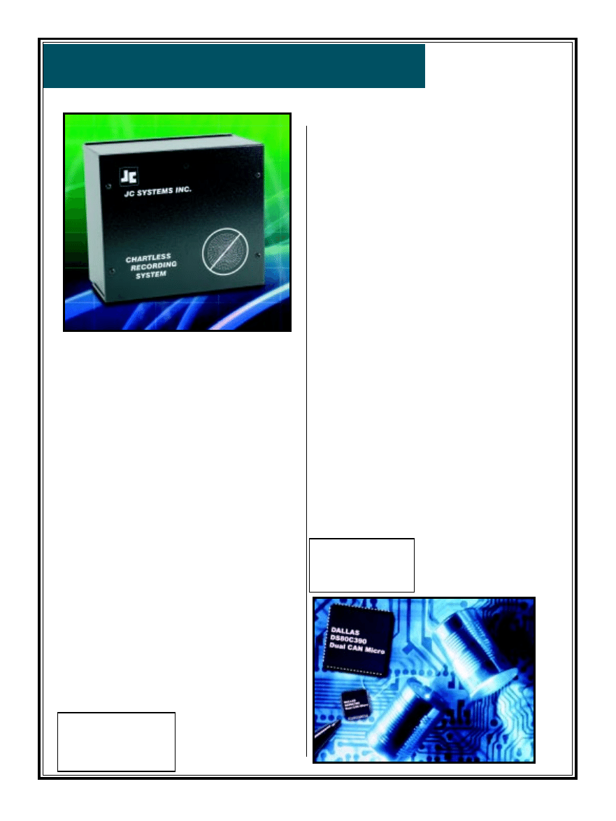
CHARTLESS RECORDING SYSTEM
The model CL2001 ChamberLog is a complete
hardware/software system that provides an alterna-
tive to circular chart recorders for logging tempera-
ture data and other physical measurements in
environmental test chambers, heat-treating furnaces,
and related applications. ChamberLog can mix and
match up to four individually configurable inputs per
chamber. Inputs can be mV, V, mA, and J, K, T, E, R,
S, or B Type thermocouples. Up to 20 ChamberLogs
(total of 80 channels) may be serially linked via RS-
485 network to any local or remote Pentium-class PC.
ChamberLog eliminates conflicts with other hard-
ware by using an independent serial network. Node
configuration and setup is as easy as providing a file
name for each chamber and the input types for chan-
nels 1–4 of each ChamberLog hardware unit on the
network. Each channel provides user-settable high
and low setpoints, with alarm indication in the form
of an audible signal and alarm message on the host
PC screen.
Users can program ChamberLog to read data at
variable scan rates up to every five seconds. Actual
logging can occur continuously, only during alarm
conditions, or at other intervals determined by the
user.
Pricing for the ChamberLog starts at $1695 and
includes hardware, software, manual, and a 3-year
warranty.
JC Systems, Inc.
(858) 793-7117
Fax: (858) 793-1931
www.jcsystemsinc.com
DUAL CAN MICROPROCESSOR
The DS80C390 dual CAN high-speed micropro-
cessor is a high-performance 8051 processor that
integrates two CAN (controller area network) bus
controllers with a host of peripherals. It exceeds
previous memory barriers by addressing 4 MB of
external data memory and 4 MB of external program
memory. The CAN protocol, a 1-Mbps serial stan-
dard, enables multiple devices to communicate in
real time along a simple bus medium in high-noise
environments. All error detection/correction, trans-
mission and reception are carried out in hardware by
the CAN controllers.
The DS80C390 delivers up to three times the
processing capability per clock cycle as a standard
8051 because of a redesigned processor core that
provides higher efficiency and eliminates wasted
clock cycles. At a maximum crystal speed of
40 MHz, the DS80C390 has an apparent execution
speed of 120 MHz.
The DS80C390 uses high-level integration to re-
duce a system’s component count and therefore, its
cost. Besides standard 8051 resources (three timer/
counters, serial port, and four 8-bit I/O ports), the
DS80C390 integrates an additional 8-bit I/O port, a
second serial port, seven additional interrupts, pro-
grammable watchdog timer, brownout monitor/inter-
rupt, powerfail reset, and a programmable IrDA clock.
In addition, 4 KB of on-chip SRAM can be configured
in various combinations of memory functions.
The DS80C390 is packaged in 64-pin LQFP and
68-pin PLCC options and sells for $7.40 in quantities
of 25,000.
Dallas Semiconductor
(972) 371-4448
Fax: (972) 371-3715
www.dalsemi.com
CIRCUIT CELLAR
®
Issue 115 February 2000
9
www.circuitcellar.com
NEW PRODUCT
NEWS
VOICE DIALING IC
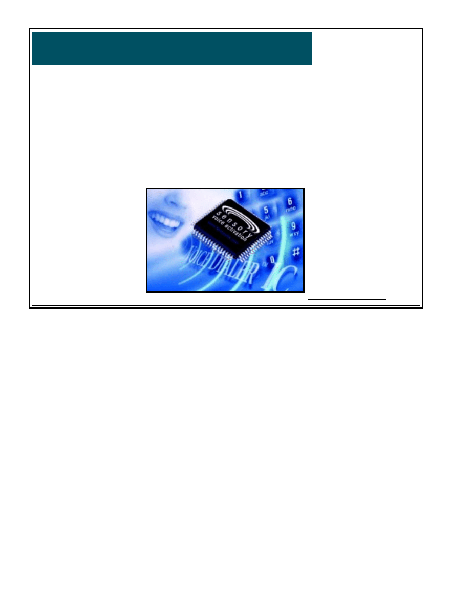
The Voice Dialer 364 ASSP adds voice dialing to hands-
free car kits, telephone handsets, PDAs, or other personal
electronics devices. The chip is a third generation prod-
uct that uses Sensory Speech 5.0 Technology and boasts a
40% increase in accuracy, lower power operation, and
many features that reduce cost and increase speed.
The Voice Dialer 364 manages a full telephone direc-
tory of names, speech recognition templates, and phone
numbers. Features include a 60-name telephone directory,
digit dialing, user-friendly
speech synthesis prompting,
digital recording and playback
for directory confirmation,
DTMF generation, and speaker-
dependent recognition for dial-
ing by name.
The Voice Dialer 364 can be
integrated into existing prod-
ucts or used to develop new
innovative applications. It
contains full software to create
a voice dialing system and is
designed to work by calling up modules that handle all
user interfacing and dialog. Using a simple 3-wire inter-
face, the Voice Dialer 364 ASSP is designed for use as a
slave chip controlled by an external host processor and
offers built in flash memory and serial EEPROM interface
drivers for storing voice recordings and phone numbers.
A Voice Dialer development kit supports Voice Dialer
364. The kit includes a suite of development tools includ-
ing Voice Dialer development kit hardware, Voice Dialer
364 software, Voice Host soft-
ware, speaker, microphone,
cables, and a manual.
The Voice Dialer IC is avail-
able as either die, or in a 64-pin
10 × 10 TQFP package and sells
for $2.65 in volumes of 100,000
(die form).
Sensory, Inc.
(408) 744-9000
Fax: (408) 744-1299
www.sensoryinc.com
Logic Analyzers
10
Issue 115 February 2000
CIRCUIT CELLAR
®
www.circuitcellar.com
NEW PRODUCT
NEWS
ETHERNET MODEM
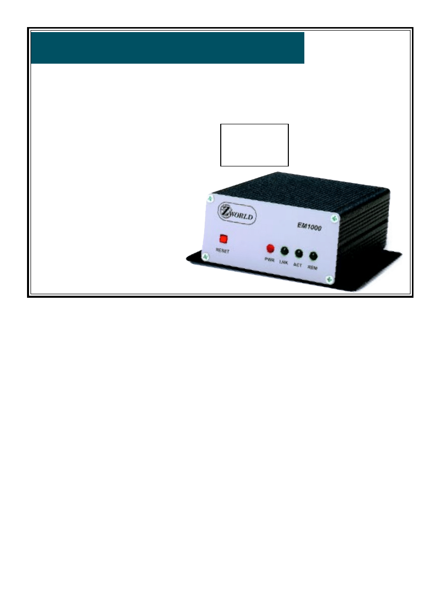
The EM1000 is an industrial-grade Ethernet modem
that allows fast communication between an RS-232 de-
vice and an Ethernet-based network. The unit provides a
dynamically reconfigurable point-to-point logical connec-
tion to other Ethernet enabled devices. It’s ideal for fac-
tory floor setups in plants with existing Ethernet
networks. Other applications include interfacing devices
such as scanners, printers, PCs, and barcode readers over
Ethernet.
The modem permits program downloads and infor-
mation exchanges between PCs, RS-232 devices, or
other mechanisms like bar-code readers and serial opera-
tor interfaces via Ethernet connections. The modem
can act as either a listener, or it can establish links
automatically or on-demand. Properly formatted
messages from controllers may also be transmitted
as e-mail, eliminating the problem of distance be-
tween the communicating devices.
The EM1000 features an RS-232 data/con-
figuration port; RS-232 configuration port;
10BaseT Ethernet port; status LEDs for
power, bus active, local active, and remote connec-
tion; and 9–32 VDC power input. Other features include
remote configuration via Telnet, multi-slave networking
ability to allow on-the-fly changes to target addresses, and
a restricted security-access mechanism.
The EM1000 sells for $299.

CIRCUIT CELLAR
®
Issue 115 February 2000
11
www.circuitcellar.com
READER
I/O
HOLD THE MISSION
In the “Asimov II” article (Circuit Cellar 113) there
was a error in Figure 1. With regard to the output cap
on U10 (LM2949-T), OUT must be at least 22 µF to
maintain stability (according to the datasheet).
I noticed the error only because I had the same
problem bite me recently!
Mike McQuade
mmcquade@aa.net
CANDLEPOWER
I enjoyed Randy Heisch’s article “Thermoelectric
Micropower Generation” in the December issue. I
tried this procedure with my thermoelectric ice chest
some years ago (ice in chest against sunny outside)
and was equally underwhelmed though interested—
now I know it’s about 0.35% efficiency.
On the milliwatt power subject, I’ve used a number
of stepper motors as generators with a hand crank. I
put a full wave bridge on each phase into two capaci-
tors, and then series them. The results are variable, but
I’ve seen 0.1 to 3 W and up to 24 VDC. Bigger motors
put out much better than the disk-drive variety.
I also cut some plastic bike pedals down to a sleeve
and bearing, and then drilled a hole in an aluminum
bike crank and fastened that into an old permanent
magnet tape handler motor. The result was 12-W output
with a fair amount of arm-warming activity.
S. Premena
premzee@juno.com
Editor’s Note: Several readers have contacted us regard-
ing the “Poisson Network” article in December’s issue.
After battling with multiple sclerosis, author Carl
Huben passed away in late November of 1999. There is
no one at Huben Consulting who can handle questions
about the article and, out of respect for the family’s
wishes, we will not forward e-mail messages or provide
family contact information at this time.

12
Issue 115 February 2000
CIRCUIT CELLAR
®
www.circuitcellar.com
Practical Analog
Circuit Design
FEATURE
ARTICLE
Craig L. King
i
Understanding a few
basic analog design
issues can go a long
way in circuit design.
Forget that old text-
book, Craig’s project
will take you from sig-
nal amplification to
calibration using a
standalone 12-bit
ADC with an 8-bit
MCU.
think it’s safe to
say that there are
some sensors out
there that wreak havoc
for certain designers. And if “op-amp
savvy” isn’t a phrase you typically
associate with yourself, then perhaps
a refresher course in analog circuit
design should be in your future. But,
who wants to spend hours with a
dusty old textbook instead of a few
hands-on hours at the bench?
Putting the fun-time on the bench
aside, practical analog circuit knowl-
edge can be crucial in many ways.
Sensor performance, cost of produc-
tion, and calibration methods can
ultimately depend on the analog front
end chosen for your application. Un-
derstanding a few basic building
blocks of analog design can go a long
way. An example of interfacing a
small signal sensor to a
stand-alone A/D con-
verter is a perfect start.
Handling a small
signal sensor with huge
errors can be difficult
when trying to maxi-
mize the resolution of
your ADC. If individual
calibration is too
costly, then careful
circuit design must
ensure that even the
sensor with the largest specified error
will still not fail.
Once you’ve maximized your ADC
resolution, you must still interpret the
data. Given a linear sensor and the
luxury of a microcontroller, a few
post-design calibration steps can turn
this into a relatively easy task. These
problems and possible solutions will
be discussed below.
A load cell is my choice for a sen-
sor, and I want to measure the force
applied to this device. I will use an
instrumentation amplifier (IA) to
amplify my signal, and control and
calibration will be done using a
microcontroller and EEPROM. Along
the way I’ll cover the signal condi-
tioning details using the IA, error
analysis of the sensor to determine a
safe gain for the amplifier, and cali-
bration methods to correct for offset
and gain errors.
CIRCUIT SUMMARY
Figure 1 shows a load-cell applica-
tion modeled by a resistive Wheat-
stone bridge. The op-amp circuit that
follows is the signal conditioning
circuit—an instrumentation amplifier.
The amplifier is built using
Microchip’s MCP602 dual op-amp.
The AD680 voltage reference from
Analog Devices is also used to condi-
tion the signal (which I’ll discuss in
detail later). Next you’ll find the
MCP3201 stand-alone 12-bit A/D
converter (ADC). Control of the con-
verter is handled by a PIC16C63,
which is connected to an EEPROM
device on the SPI bus.
As pressure is placed on the load
cell, a differential voltage appears
across the two output terminals rela-
tive to the strain on the sensor. This
Figure 1
—In the pressure-sensing circuit, the load cell is represented by the
Wheatstone bridge on the left. The instrumentation amplifier was built using the
MCP602 dual op-amp package and the AD680 was used as the offset voltage.
The MCP3201 12-bit ADC is the converter, using V
DD
as the reference voltage.

CIRCUIT CELLAR
®
Issue 115 February 2000
13
www.circuitcellar.com
voltage is the input to the IA circuit,
which introduces gain and offset volt-
ages to condition the ADC signal. The
resulting voltage is then sampled by
the ADC, which sends the resulting
digital word to the microcontroller for
data interpretation and processing.
THE LOAD CELL
So how does this device work? As
mentioned earlier, the sensor outputs
a differential signal relative to the
pressure placed on the device. This
differential signal is small, <20 mV
full-scale output in either direction
for a 5-V system. Bending the load cell
in one direction causes a differential
voltage to appear across the two out-
puts. Bending the cell in the opposite
direction reverses the polarity on the
output. Table 1 lists some of the load-
cell specifications. Keep in mind that
we are designing the analog front end
to accomodate the sensor with the
largest specified error.
You will notice right away the
huge errors of this device, especially
the 20% full-scale error and zero-
balance error. The signal output from
this device is so small compared to
the input range of our ADC that sig-
nal gain will be necessary.
INSTRUMENTATION AMPLIFIER
For those of us unfamiliar with
designing-in an IA, it should be noted
that using an IA isn’t as daunting a
task as you might think. Neverthe-
less, before you ask how, let me first
address why. You know that the sen-
sor outputs a differential signal on a
relatively small scale (<20 mV full-
scale output in either direction). The
resistance of the load cell is specified
as 1200-
W
±
300 (see Table 1).
The IA is an excellent
solution for isolating the
sensor from the ADC. The IA
has two high-impedance
inputs that minimize current
loss from the sensor, protect-
ing us from the resulting
voltage drop across the sensor.
The amplifier’s low im-
pedance output also buffers
the ADC input pin. But, it is
the differential high-imped-
ance inputs of the IA that
make it a prime choice to amplify this
sensor’s output. The load-cell sensor
requires an offset voltage and a signal
gain. Using the IA, a single resistor
can be used to change the gain.
As shown in Figure 1, this is a two
op-amp IA built using the MCP602
single-supply op-amp. The difference
between the two inputs is gained by
whatever the gain is set for the cir-
cuit. This result is also offset by
whatever the reference voltage is.
This reference voltage is not ampli-
fied, it merely passes through and is
added to the output.
For example, assume the gain for
the IA is set for 300 and the difference
between the outputs (IA+ minus IA-) is
1.5 mV. Therefore, the 1.5 mV is
gained by 300, yielding 450 mV. Then
the offset of 2.5 V is added to get
2.95 V. This offset voltage can be used
to position the output around a central
voltage, as we will see with the ADC.
The IA circuit handles the signal
conditioning for the sensor. As dis-
cussed, offset voltage and a gain factor
can both be introduced to the signal
using the IA. Let us compare the raw
signal coming from the sensor to our
intended output as it reaches the
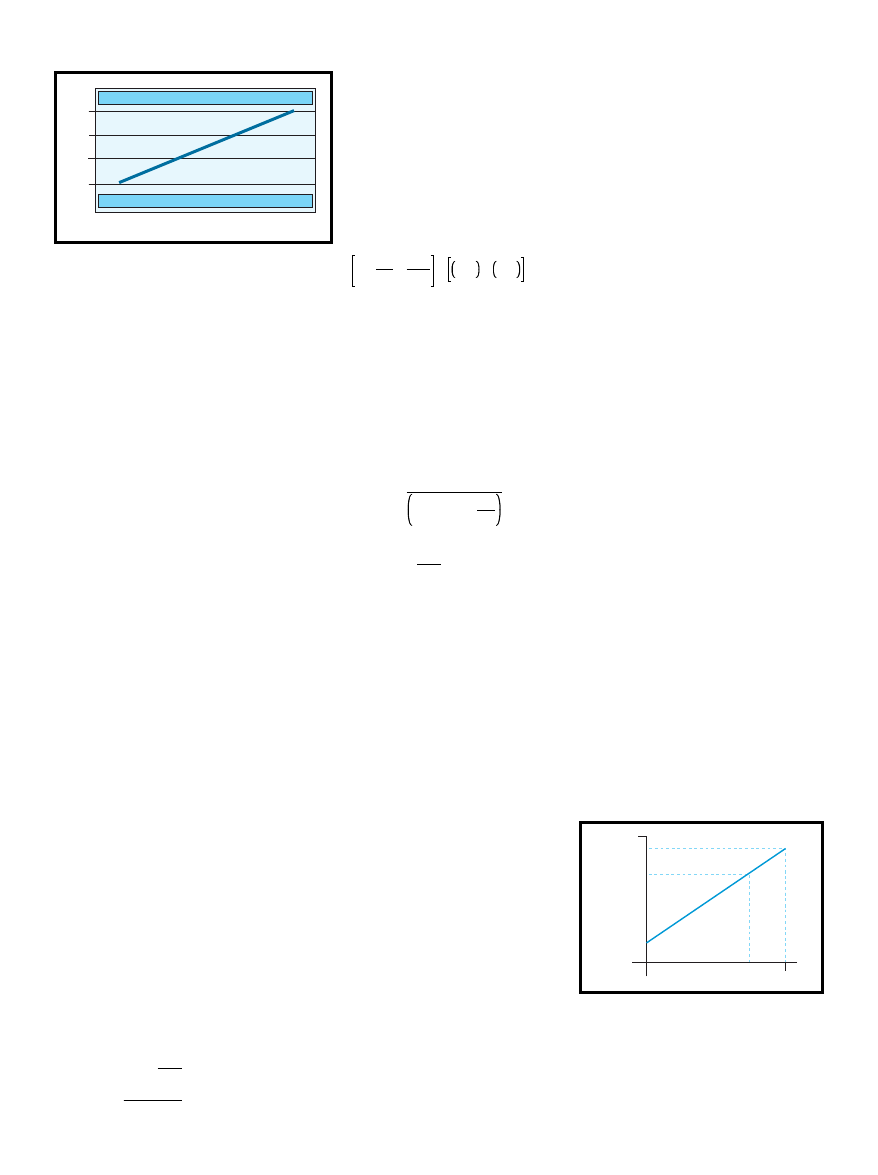
ADC. Figure 2 shows this graph. The
left side y-axis represents the output
of the signal directly from the
sensor. The right side y-axis
represents the intended IA out-
put going into our ADC.
For this example, I intend to
measure the load-cell deflection
resulting from pressure from
either side. Due to the nature of
the resistive bridge, the differen-
tial voltage between the outputs
will be positive or negative de-
pending on the direction of the
deflection. Therefore, the signal re-
quires an offset of 2.5 V to center it
between the input rails of our ADC,
which is 0–5 V for this example. The
gain that is applied will then expand
the signal to the 0–5-V range of the
ADC. So, how do I determine exactly
what the gain should be?
GAIN: BETTER SAFE THAN SORRY
As we discussed, the IA gains the
difference between its two inputs and
offsets this value by whatever the
reference voltage is. This transfer
function for this dual op-amp instru-
mentation amplifier can be written as:
IA output =
Gain × Difference + Offset
IA output =
1 + RI
R2
+ 2R1
Rg
×
IA+ – IA– + V
ref1
Notice that the gain is a function
of all three resistors in the IA circuit.
It’s your job to determine what the
gain should be.
Recall from our discussion the
sensor errors that are associated with
this load cell. Each load cell has a
possible 20% error. It’s our goal to
ensure that every load cell on every
system, regardless of its error, will
work in our circuit up to full scale.
If the decision is made not to indi-
vidually calibrate the gain, then you
must design-in a gain that will be
suitable for all systems. You must
take into account the errors associ-
ated with the sensor, and design your
gain using the worst-case full-scale
output based on these errors.
So, what would the worst-case full-
scale output be? A simple error analy-
sis of our sensor will solve this
Table 1
—The rated output and zero balance errors will affect your
instrumentation amplifier gain calculation.
Specification
LCL-816G
Rated capacity
32 oz (896 g)
Excitation
5 VDC to 12 V (max)
Rated output
2 mV/V ±20%
Zero balance
±mV/V
Operating temperature
–55° to 95°C
Compensated temperature
–5° to to°C
Resistance
1200
W
±300
W
Safe overload
150%
Full-scale deflections
0.01
²
to 0.05
²
Figure 2
—The left-hand data series represents the output of
the sensor on a scale of mV. The right-hand data series repre-
sents the input range of the ADC (in volts) that you are attempt-
ing to use. As you can see, both an offset voltage and a signal
gain will be necessary to make this transition.
50
0
–50
–100
100
6
5
4
3
2
1
0
–FS Deflection FS
Sensor output (mV)
Ideal A/D input (V)
14
Issue 115 February 2000
CIRCUIT CELLAR
®
www.circuitcellar.com
problem. Relevant specifications from
the load-cell data sheet (see Table 1):
Full-scale (FS) output: 2 mV/V
±
20%
Zero balance:
±
0.3 mV/V
(2 mV/V ) × (5 V) = 10 mV
(0.3 mV/V) × (5 V) = 1.5 mV
For this 5-V system, the resulting
worst-case full-scale output is
11.5 mV. Do any op-amp specifica-
tions affect the gain calculation? Yes.
Any offset voltage associated with an
op-amp will be amplified and will
appear in the output.
The relevant specification from the
op-amp datasheet is:
Offset voltage:
±
2 mV at 25°C
Because the IA uses two op-amps,
you must include both worst-case
offset errors in your calculation,
which results in a possible total of
4 mV offset error to be included.
Therefore, our new worst-case full-
scale output is 15.5 mV.
Figure 2 shows the relation be-
tween the sensor output and the A/D
input range. You can see now that the
reference voltage offset of the IA will
help you in shifting the differential
signal up to an entirely positive range.
By shifting the differential signal
by 2.5 V, you are able to gain the sig-
nal. You are now centered between
the rails of the ADC range of 0–5 V.
Using the above worst-case full scale
output, you can calculate your gain as:
V
out
V
in
= Gain
(5.0
2.5)
15.5 mV
= 161.3
So, how can you implement
this value in the circuit? As
discussed, the dual op-amp IA
for this application uses the
following transfer function:
IA output =
Gain × Difference + Offset
IA output =
1 + RI
R2
+ 2R1
Rg
×
IA+ – IA– + V
ref
The first set of parenthesis repre-
sents the gain. Keeping R1 and R2
constant, you can use Rg as your gain
selector. Using 1% values of 30k and
10k for R1 and R2, respectively, you
can then calculate a value for Rg
based on our previous gain calculation
of 143.
Rg =
2R1
Gain – 1 + R1
R2
Rg = 20k
90
= 123
Ω
Now, keep in mind that this gain
was calculated for a worst-case sce-
nario. Our design approach was to
accomodate the worst-case signal,
instead of spending the money for a
post-production calibration step. Fig-
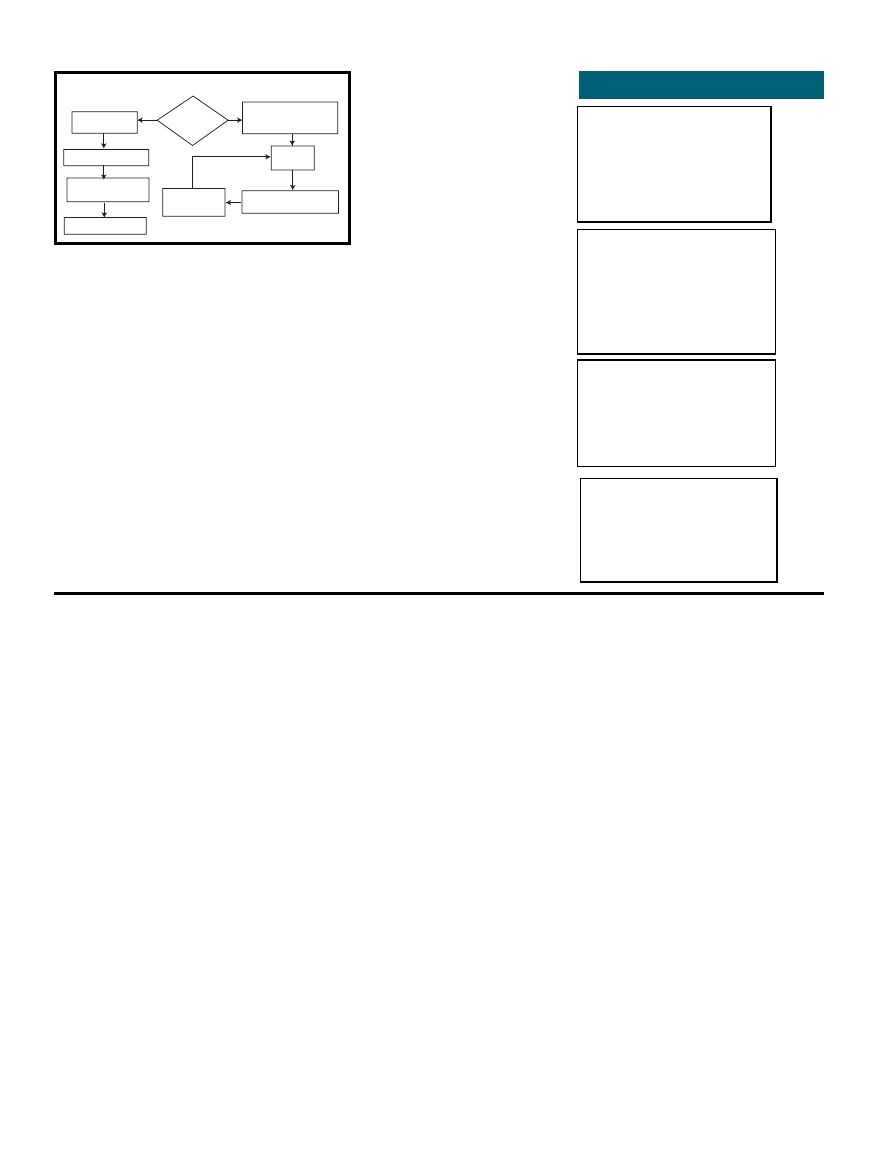
ure 3 shows how the huge errors asso-
ciated with this gain calculation can
affect the resolution of the ADC. The
bands at the top and bottom of the
ADC range show the resolution lost
due to this error compensation. How-
ever, the error compensation was
necessary to ensure that every load
cell would still work in the circuit at
full scale.
Given the luxury of post-produc-
tion gain calibration, you could easily
adjust the gain on each board sepa-
rately by using a 500-
W
potentiometer
in place of Rg. A production specialist
could then place a full-scale positive
reference pressure on the load cell and
then adjust the gain of the IA until
the output approaches the ADC refer-
ence voltage of 5 V.
Of course, the tradeoff would be an
increased cost per unit to make up for
the post-production calibration step.
However, if this is not an option, you
can rest assured that the original gain
calculation will still accommodate
even the worst sensor.
THE DIGITAL SIDE
Now that the analog front-end is
complete, you can concentrate on the
digital domain (i.e., how you interpret
the digital data from the ADC). Are
there better methods of calibrating
your system using firmware?
Can this calibration step also be
used to form a relationship between
the ADC data and the output of our
system (pressure)? Depending on the
output of the sensor, the answer could
be a resounding “Yes!” And for this
sensor, you’re in luck. The output of
this system is extremely linear. In
fact, it’s close enough to a straight
line that you could use two-point
linear interpolation.
And how exactly could this be
done? Given two known pressures
from the load cell and their resulting
digital words—any other value would
fall on, or close to, a straight line
passing through the two points (see
Figure 4). Two points define a line,
and by taking two ADC samples at
known forces, you then have the equa-
tion for your line. Storing these values
in EEPROM enables you to individu-
ally calibrate each system one time.
The linear interpolation process
requires a few simple math operations
to determine the resulting data. Be-
cause of the 12-bit word length from
our converter, the 16-bit unsigned
math routines from the PICmicro
Figure 4
—Linear interpolation enables you to deter-
mine the pressure/deflection of the load cell based on
the two endpoints of the line. Calibration is performed
by saving (to EEPROM) the ADC code of the two
endpoints, which is measured using known reference
pressures. Y
full
and Y
zero
are the stored calibration
constants. A sampled ADC code ( Y
sampled
) can then be
used to calculate the resulting load-cell deflection.
Y
full
Y
samlpe
ADC
digital code
Y
zero
0000
0 Zero scale
X?
4095
Full scale
Figure 3
—This graph shows the output of the instrumentation
amplifier for an ideal load cell using the gain calculated through
error analysis. The unused voltage areas at the top and bottom
of the graph are necessary for that worst-case sensor.
5
4
3
2
1
0
– FS Deflection FS
Possible sensor error
Possible sensor error
IA output (V)
CIRCUIT CELLAR
®
Issue 115 February 2000
15
www.circuitcellar.com
Figure 5
—This example firmware flow uses linear interpolation to
display the correct pressure, which is possible because of the
linearity of the sensor.
Measure zero
reference
Write to EEPROM
Measure full
scale reference
Write to EEPROM
Enter
calibration
mode?
Read calibration
values from EEPROM
Sample
A/D
Use calibration values
to determine deflection
Display
correct value
Yes
No
RESET
SOURCES
Load cell
Omega Engineering, Inc.
(800) 826-6342
(203) 359-1660
Fax: (203) 359-7700
www.omega.com
AD680
Analog Devices
(800)-ANALOGD
(617) 329-4700
Fax: (617) 329-1241
www.analog.com
SPI
Motorola
(512) 328-2268
Fax: (512) 891-4465
www.mot-sps.com
MCP3201, MCP602
Microchip Technology Inc.
(480) 786-7200
Fax: (480) 899-9210
www.microchip.com
Craig L. King is an applications engi-
neer for Microchip Technology’s
Microperipheral Products division.
You may write to him at craig.king
@microchip.com
math library could be used to simplify
firmware development.
Figure 5 shows example calibration
steps. This example uses zero and
positive full scale as the endpoints for
the line. The values are saved to
EEPROM once during calibration and
the microcontroller reads these values
during normal operation on reset.
SCRATCHING THE SURFACE
Depending on the desired accuracy
of the system, a simple offset and gain
correction, along with an appropriate
method of calibration, can be most of
the work. But, if your applica-
tion requires getting 11+ bits
out of your 12-bit ADC, there
are many other issues that
cannot be ignored. Safe layout
practices, ground planes, by-
pass capacitors, and device
positioning are just a few noise
issues that could easily sink
your circuit design if not paid
proper attention.
Before you spend the time
squeezing those last few bits
out of your converter, you must first
have a circuit to squeeze. A simple
instrumentation amplifier circuit
might be the perfect place to start
your design. Remember that there are
entire books written on some of the
topics discussed, so you probably
shouldn’t run right out and have that
T-shirt made that says “Op-amp
Savvy” just yet.
I

16
Issue 115 February 2000
CIRCUIT CELLAR
®
www.circuitcellar.com
Build An AVR
Programmer
FEATURE
ARTICLE
Stuart Ball
i
If you’ve been looking
for an inexpensive
way to program
Atmel’s AVR micro-
controllers, then
Stuart’s project is just
what you need. With
a little work and only
six ICs, you can build
a programmer that is
perfect for working
with AVR parts.
f you’ve wanted
to experiment with
the Atmel AVR-series
microprocessors but
needed a cheap way to program them,
this project is for you. Using only six
ICs, you can start programming and
experimenting with the AVR parts.
The AVR 90S-series microproces-
sors from Atmel are RISC-based
microcontrollers. There are currently
four parts in the family, the
AT90S1200 and ’S2313 (in 20-pin
packages), and the AT90S4414 and
’S8515 (in 40-pin packages). Table 1
shows the key differences between the
parts. For a brief description of the
AVR architecture, see “What’s the
Count” in Circuit Cellar 112.
All AVR devices have 32 general-
purpose registers. On the AT90S1200,
this is the only RAM available. The
other devices in the series have addi-
tional RAM, as indicated in Table 1.
The AVR parts use flash memory
to store programs. The flash memory
can be electronically erased and repro-
grammed, so there’s no need to have a
UV eraser sitting by the programmer.
Atmel provides two methods to
program the flash memory—serial and
parallel. The serial method uses three
pins on the device and does not re-
quire any power supply other than the
normal 2.7–6-V supply voltage. The
serial method is suitable for program-
ming the devices in-circuit. However,
there is a fuse (SPIEN) in the device
that can be set to disable serial pro-
gramming. If this fuse is programmed,
serial programming and reading of the
device cannot be performed.
The parallel programming method
uses eight data lines and seven control
lines. This method also requires that
+12 V be applied to the reset pin to
enable programming. The parallel
method requires more hardware but
works regardless of the state of
SPIEN. The programmer design for
this project uses the parallel method.
Programming the AVR in parallel
mode redefines the normal pin func-
tions as shown in Table 2. Unlike a
PROM, the AVR processor doesn’t
have separate address lines to select
the location to be programmed. In-
stead, the address is written as two 8-
bit data values using the data lines.
The eight data lines get the program-
ming address, programming data, and
commands that tell the AVR what
programming operation to perform.
The AVR drives –BUSY low when
it starts to program a byte, and back
high when programming is finished.
This provides a means for the pro-
Table 1
—The four AVR devices have different amounts of on-chip RAM and flash memory. The 40-pin devices have
more internal memory than the 20-pin devices, as well as more I/O pins.
AT90S1200
AT90S2313
AT90S4414
AT90S8515
Pins
20
20
40
40
Flash memory
1 KB
2 KB
4 KB
8 KB
EEPROM
64 bytes
128 bytes
256 bytes
512 bytes
RAM
32 bytes
128 + 32
256 + 32
512 + 32
I/O Pins
15
15
32
32
8-bit timers
1
1
1
1
16-bit timers
0
1
1
1
UART
0
1
1
1

CIRCUIT CELLAR
®
Issue 115 February 2000
17
www.circuitcellar.com
grammer to determine when a byte is
finished programming.
The –OE signal goes low to enable
the AVR outputs for reading. The
–WR signal tells the AVR to start
programming a byte and is pulsed low
after the command, address, and data
have been loaded.
BS selects either the low or high
bytes of address and data. When BS is
low, the low address or data byte is
read or written, and when BS is high,
the high byte is read or written. XA0
and XA1 determine whether the data
on the data lines is a command, ad-
dress, or data byte. XA0 and XA1 are
defined as:
XA1
XA0
0
0
Address
0
1
Data
1
0
Command
Finally, the clock pulse on the crys-
tal input pin clocks the command,
data, and address bytes into the chip.
The AVR devices also have an
EEPROM that can be written by the
processor under program control or
programmed externally. There is also
a device signature that identifies the
device type and a pair of lock bits.
The lock bits can be used to prevent
anyone from reading the contents of
the device. The lock bits and SPIEN
fuse can be cleared only by erasing the
entire device.
The Atmel parallel programming
mode supports chip-erase, program-
ming and reading of the flash memory
and EEPROM, and reading the fuse
and lock bits along with the device
signature bytes.
Programming a location in the
AVR involves placing a command on
the data bits, setting XA0/XA1 to
two, and toggling XTAL1. Then, the
high address is placed on the data bits,
XA0/XA1 is set to 0, –BS is set to 1,
and XTAL1 is
toggled again. A
similar procedure
is followed to load
the low address
byte and the data
byte. Then –WR is
pulsed low to start
programming.
When program-
ming is complete,
the AVR drives the –BUSY bit high.
Although the AVR has a program
word that is 16-bits wide, the word is
programmed one byte at a time. Fig-
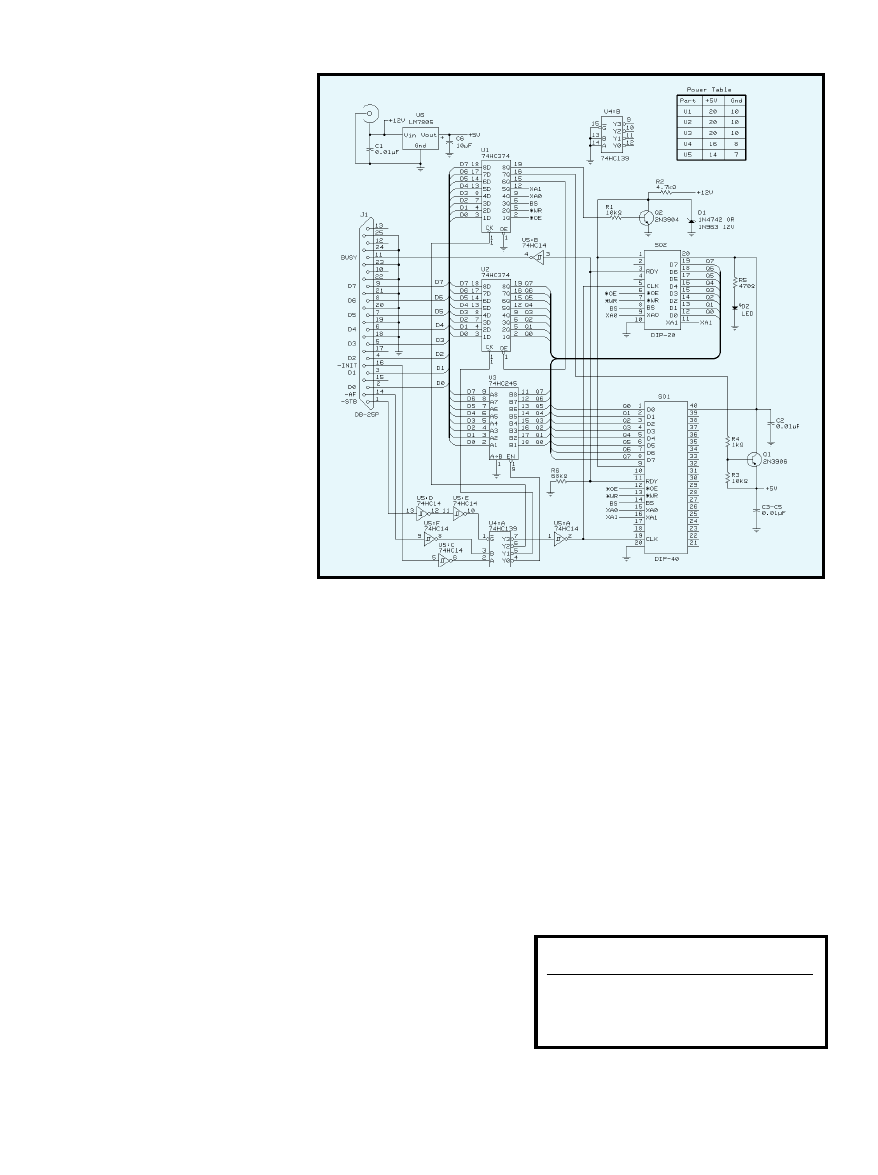
ure 1 shows the waveform used for
programming the low byte of the
word. The same sequence is followed
for the high byte except the BS line is
high when the data byte is loaded.
The process of reading the AVR
device is similar to writing, except
that the read command is issued and
the –OE signal (instead of –WR) is
pulsed low to enable the AVR out-
puts. Before programming, the pro-
grammer software erases the device
using the erase command. The AVR
does not use the –BUSY bit to indicate
when the erase is complete so erase
timing is up to the programmer.
Command bytes are 0x80 to erase
the chip, 0x10 to program the flash
memory, and 0x02 to read the flash
memory. The AVR commands for
reading/programming the EEPROM
and for reading/programming the fuse
and lock bits are not implemented on
this project.
You can download an assembler for
the AVR microcontrollers from the
Atmel web site.
PROGRAMMER FEATURES
The AVR programmer provides
capability to program all four of the
Atmel AVR devices. Two ZIF sockets
are provided, one for 20-pin and one
for 40-pin parts. The programmer
plugs into the parallel printer port of a
PC. Windows 95 software to use the
programmer is available on the Cir-
cuit Cellar
web site.
The programmer circuit connects
to the parallel printer port of a PC. As
you can see in Figure 2, U2 is a 74HC-
374 that latches and buffers the data
bus to the AVR. U3 is a buffer that
allows the data bus to be read. U1
drives the control inputs to the AVR
device. U4 decodes the control lines
from the printer port to latch data,
read data, or clock data into the AVR.
The printer signals –AF and –INIT
are used to select which register on
the programmer is written or read.
These pins are defined in Table 3.
To perform one of these operations,
the –AF and –INIT lines are set to the
correct state, and the –STB signal (pin
1) is pulsed low. This causes the ap-
propriate output of U4A to pulse low.
To read data, the programmer has
to turn off the printer port output
buffer and the data register on the
programmer. If the data buffer on the
port was left enabled, there would be
a bus conflict with U3, and if the data
register on the programmer was left
enabled, there would be a bus conflict
with the AVR device when it turns on
its outputs.
The printer port buffer is disabled
by writing to a bit in the printer port
control register (different from the
programmer control register, U1). To
disable the programmer data register,
Figure 1
—The timing diagram
for programming a single byte
in the AVR device is shown
here. Data, address, and
commands are written to the
device using the 8-bit data bus.
PB0–PB7
0x10 (PROGRAM COMMAND)
ADDR LOW
ADDR HIGH
DATA LOW
XTAL 1
*WR
BS
XA1, XA0
10
00
00
01
Table 2
—In programming mode, the pins of the AVR device are redefined as shown.
Program mode is entered by bringing the V
PP
pin to +12 V.
Pin
Definition
PB0–PB7
Data and command input/output
PD1
–BUSY feedback bit
PD2
–OE (Output Enable)
PD3
–WR (Write Enable)
PD4
–BS (Byte Select, selects high or low byte)
PD5, PD6
XA0 and XA1, address inputs
Crystal1
Clock pulse
18
Issue 115 February 2000
CIRCUIT CELLAR
®
www.circuitcellar.com
bit 5 of the programmer control regis-
ter is set high, driving the output-
enable pin (pin 1) of the programmer
data register (U2) and tristating the
outputs.
The read data buffer, U3, is a bidi-
rectional device, but the direction pin
(pin 1) is grounded, allowing transfers
in only one direction. Because the
AVR programmer uses the printer
port data lines for both reading and
writing, a bidirectional printer port is
required.
The bits in the control register (U1)
are defined in Table 4. The –BUSY bit
from the AVR is buffered by U5B
(pins 3 and 4) and drives pin 11
of the printer port connector.
This is the printer BUSY signal
and is monitored by reading
the printer port status register.
SO1 and SO2 are 40- and 20-
pin ZIF sockets for program-
ming the AVR device. Q1
supplies +5 V to the AVR
socket and the LED (D2) lights
when +5 V is applied.
The input power supply is a
12-VDC wall-wart transformer. Be
sure to use a supply with a DC out-
put, not AC.
Twelve volts is enabled by Q2.
When output D7 of the control regis-
ter (U1–19) is high, Q2 is saturated
and the voltage at the 12-V pin of the
AVR is 0 V. The actual voltage is the
saturation voltage of Q2, but that will
typically be 200 mV or so.
When output D7 of the control
register goes low, Q2 is turned off and
resistor R2 pulls the AVR 12-V input
up to the 12-V supply. The AVR
doesn’t draw significant current from
Figure 2
—Because the AVR programmer requires only six ICs and two transistors, you can build this programmer
and start experimenting with AVF parts in no time.
Table 3
—The –AF and –INIT pins on the printer connector (pins
14 and 16) select which programmer register will be written or
read. The –STB signal (pin 1) is driven low to actually read the
data or clock the register.
Pin 14
Pin 16
(–AF)
(–INIT)
Function
0
0
Pulse AVR clock input
0
1
Write control register
1
0
Write data register
1
1
Read data from AVR
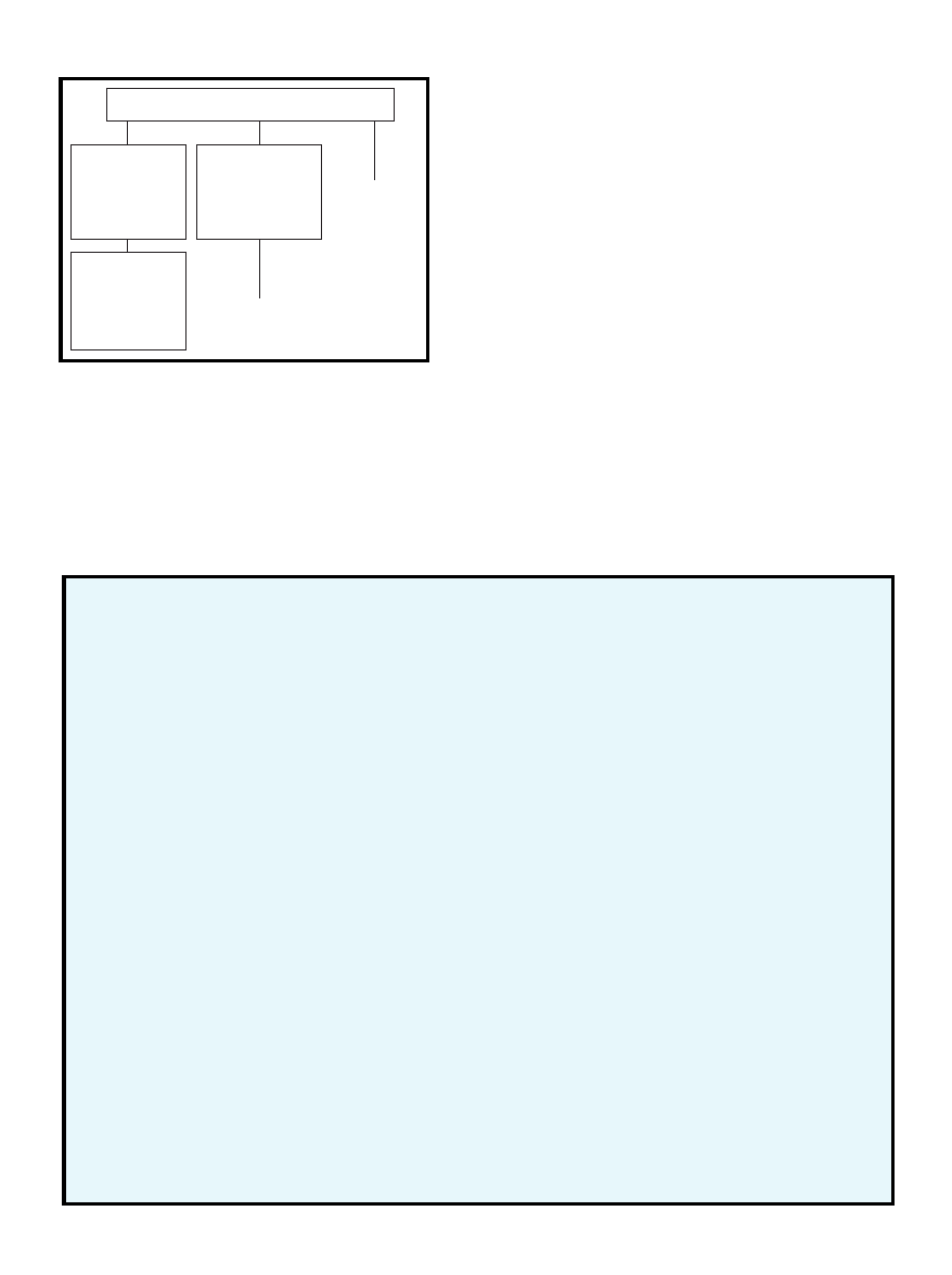
20
Issue 115 February 2000
CIRCUIT CELLAR
®
www.circuitcellar.com
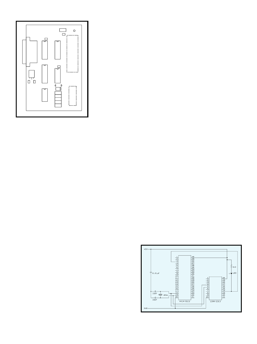
Figure 3
—The software inter-
faces uses a standard Windows
dialog box. The software is
partitioned into low-level code
that communicates with the port,
AVR-specific code that performs
device-level functions, and code
that communicates with Windows.
Windows dialog application
AVR support routines
Power on/off
12 V on
AVR read
AVR write
Erase
Hex file support routines
Get record length
Get address
Get record type
Get data word
C++ file open dialog
C++ CFile functions
Low-level interface
Write command register
Write data register
Read data
Wait for not busy
Convert ASCII to hex
Pulse AVR clock
File Formats
The Intel-format hex file was developed by Intel
in the early days of microprocessors, when data was
typically read from a paper-type reader attached to a
teletype machine. The file consists of a series of one-
line records, terminated by an end-of-line character.
All the data is in ASCII, and each record uses the
following format:
:LLAAAATTDDDDDDDDDD….CC
where the colon character (:) starts each line, LL is
two hex-ASCII characters that define the number of
data bytes, AAAA is the starting address for the data
on the line (four hex-ASCII characters), TT is the
record type (00 for data record, 01 for the last record
in the file), DD is the data (two characters per byte),
and CC is a one-byte checksum.
The AVR microcontrollers use a 16-bit wide flash
memory, so the data is ordered as pairs of bytes to
make a word. The low byte of each pair is sent first,
followed by the high byte.
A line from a hex file for the AVR devices looks
like:
:100020000EBD00E00BBD08EC0ABD00E000E00DBD18
This line describes a hex record with a length of
16 bytes (10h), starting at address 0020 (hex). The
record type of 00 indicates that this is a data record.
This is illustrated by:
10 (length) 0020 (starting address) 00 (record type)
The first few bytes of data for this line are 0E BD 00
E0 0B BD 08 EC. These would be programmed into an
AVR device as words, like:
BD0E E000 BD0B EC08
The one-byte checksum at the end was an important
feature when data was sent using electromechanical
paper tape readers. In a disk-based system, a bad read
will result in a CRC error from the disk controller. The
checksum in the file is redundant, and the software for
the AVR programmer ignores it.
The four character address value limits the Intel for-
mat to a maximum of 64k addresses. There is also an
extended Intel hex format that provides a larger address
space by defining a third record type.
Although the programmer software doesn’t support it,
the Atmel assembler is capable of generating Motorola-
format hex files. The Motorola format looks like:
S1LLAAAADDDD…CC
where S1 is the start sequence, LL is the length of the
record (in bytes), AAAA is the address DD is the data,
and CC is a two-byte checksum.
the +12-V input, the high voltage is
used to put the device into parallel
programming mode. Most 12-VDC
transformers produce an output of
15 V or so when lightly loaded, so D1
clamps the voltage to 12 V at the AVR.
Transistor Q1 is a PNP type,
2N3906. When output D6 of the con-
trol register (U1–16) is high, resistor
R3 pulls the base of Q1 to +5 V, turn-
ing Q1 off. When control register D6
goes low, the base of Q1 is pulled
toward ground through R4. This satu-
rates Q1 and applies +5 V to the AVR
sockets. This also turns on the LED.
R6 ensures that the –BUSY bit will
be low if no AVR device is installed in
either socket, which will produce a
device error. Without R6, an attempt
to program an empty socket may not
detect the error until verify.
Finally, U6 (a 7805) regulates the
+12-VDC input to produce 5 V for the
logic and the Atmel devices.
ABOUT THE SOFTWARE
The software was written in
Microsoft Visual C++, as a Win 32 app
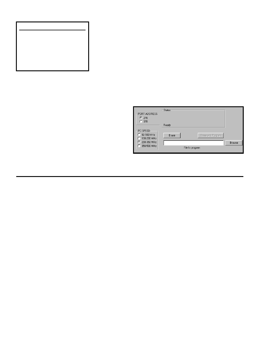
for Windows 95. Photo 1 shows the
dialog box for the programmer soft-
ware. Two clickable buttons are pro-
vided, one to Erase and one to Erase
and Program. The Erase button issues
an erase command to the device. No
erase verification is performed.
To program a device, a file must be
selected. The programmer software
requires an Intel-format hex file (see
the File Formats sidebar for more
information). The Atmel assembler
enables you to select either Motorola
S-record or Intel-format files. The
CIRCUIT CELLAR
®
Issue 115 February 2000
21
www.circuitcellar.com
filename may be typed into the edit
field or you can click the Browse but-
ton to bring up the standard Windows
95 open-file dialog box to select a file.
The Erase and Program button is
grayed out until you select or enter a
filename. Clicking this button will
erase the device and then program it
with data from the selected file. If you
enter a file that doesn’t exist, you will
get a file error.
The software provides radio but-
tons for selecting the port address
(0x278 or 0x378) and a speed-compen-
sation value for the speed of your
CPU. The speed compensation con-
trols the amount of settling time
between successive operations to the
printer port and the timeouts for de-
tecting device errors and erasure. The
compensation value isn’t critical, but
if you get device errors while pro-
gramming, try a different value.
Finally, the software provides a
4-line status box where messages are
displayed. The box will display the
current address as each hex record is
programmed and the location of any
errors that occur. Messages scroll up
during operation
and the last four
are displayed.
The software
doesn’t check for
the correct device
size, so if you try
to program 8 KB
of data into a 1-
KB device, it will
let you. Of
course, you’ll get
a verify error. The
Table 4
—U1 controls various programmer functions.
Five bits connect directly to the AVR sockets, one
enables the data register, and two turn the +5-V and
+12-V on and off.
Bit
Definition
D0
Drives AVR –OE signal
D1
Drives AVR –WR signal
D2
Drives AVR BS signal
D3
Drives AVR XA0 signal
D4
Drives AVR XA1 signal
D5
1 disables data register U2
D6
0 turns on +5 V to AVR
D7
0 turns on +12 V to AVR
Photo 1
—There are only five user functions—selecting a file, erasing a device,
erasing/programming a device, selecting the parallel port address, and selecting the
compensation value for CPU speed.
software also doesn’t check that the
file you select is a valid hex file, al-
though almost any other type of file
will produce file or device errors.
The software was created using the
Microsoft C++ wizards to format the
dialog box and buttons. The program-
ming code was originally developed as
a console application, then the pro-
gramming routines were incorporated
into the Windows dialog shell.
Figure 3 shows the software struc-
ture. The Windows dialog application
passes control to other, lower-level
functions when you click on a button.
22
Issue 115 February 2000
CIRCUIT CELLAR
®
www.circuitcellar.com
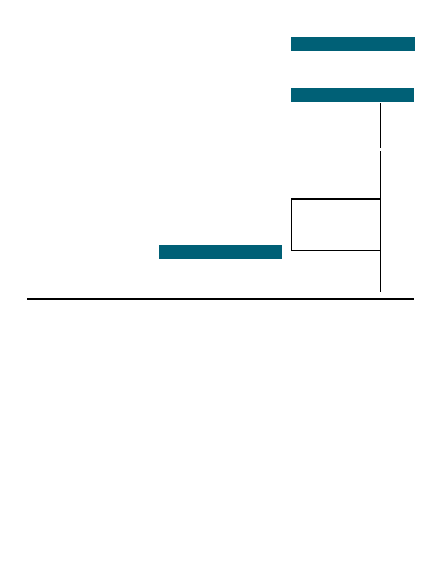
Figure 4
—Note that SO1, SO2, and the LED are
mounted on the back of the board to simplify mounting.
J1
U1
U3
U2
U6
U5
U4
SO1
SO2
LED
C2
R5
C1 C3
Q1
Q2
C5
R2
R1
R4
R3
R6
D1
C4
Figure 5
—If you program the test files, TST2313.HEX or TST4414.HEX, into
the appropriate device and plug it into this test circuit, the LED will blink. This
test will show you if the programmer is wired correctly.
The AVR support routines provide
functions such as programming a
single location, reading a location,
etc. These functions call lower-level
routines that actually read and write
the hardware registers on the pro-
grammer via the parallel port.
CIRCUIT CONSTRUCTION
The prototype was constructed on
perfboard and wired point-to-point.
Figure 4 shows the parts layout that
was used and the parts list is available
on the Circuit Cellar web site. Use a
grid of copper EMI tape under the ICs,
or some other means to get a good,
low-impedance ground. SO1 and SO2
are located on the bottom of the board
to make final mounting easier. The
completed project was mounted in a
plastic case with holes cut in the top
for the ZIF sockets and LED.
The power supply is a 12-VDC
wall-wart transformer. Anything that
can supply 300 mA or more will be
adequate. A 2.1-mm coaxial jack is
mounted on the plastic case for con-
nection to the supply. The schematic
shows 74HCxxx parts. You can use
74HCT or 74ACT as well.
The two ZIF sockets, SO1 and SO2,
are mounted on the back of the board
to simplify mounting the board in the
case. The 40-pin ZIF sockets are
manufactured by 3M, Aries, and other
manufacturers, and are readily avail-
able from numerous sources, such as
Digi-Key. As for the 20-pin ZIF sock-
ets, they were common when a lot of
PLDs were in 20-pin DIP packages.
3M/Textool still makes them and
they are listed in the Digi-Key catalog.
If you can’t find the 20-pin socket,
or you want a lower-cost alternative,
you can substitute a 24-pin socket and
use only the lower 20 pins. If you do
this, be sure to route the connections
to the right pins and select a socket
(such as the Aries24-65xxx series) that
accepts an IC that’s 0.3
²
wide.
If you don’t plan to program many
devices, you can use machined-pin
sockets for SO1 and SO2. They obvi-
ously won’t last as long as the ZIF
sockets. And, if you plan to work only
with the 20-pin devices, you can leave
off the 40-pin socket and vice-versa.
TESTING
Three test files are provided—
TST4414.HEX
, TST2313.HEX, and
TST1200.HEX
. TST4414.HEX is for
’90S4414 and ’90S8515 devices,
TST2313.HEX
is for ’90S2313 devices,
and TST1200.HEX is for the ’90S1200.
All of the files just blink an LED to
verify that the programmer works.
Figure 5 shows a circuit that con-
nects a 40- and 20-pin socket to use
the test software. The crystal on the
test board isn’t critical—anything
from about 3 MHz up to 10 MHz will
work. If you’re confident in your wir-
ing abilities, you can skip the test
circuit.
Using the programmer is fairly
simple. Plug the programmer into the
parallel port and plug in the 12-V
supply. When you
connect the program-
mer to the computer,
use a short cable, 6
¢
or
less. Avoid ribbon
cable because the
crosstalk between the
wires tends to be high
and may cause errors.
From Windows
Explorer, double click
on the AVRBURN.EXE
file to start the pro-
grammer software.
Select the file you
want to program and
install the AVR device
into the appropriate socket. Click the
Erase and Program button and the
programmer will erase, program, and
verify the part. If you just want to
erase a device, don’t select a file.
Even though there are two sockets,
you can only program one part at a
time. Using two sockets eliminates
the need for a set of jumpers that
would be required to configure a
single socket for both device types,
but it doesn’t allow programming of
two devices at once. If you try to do
that, you’ll get bus contention on the
–BUSY bit as both devices try to drive
it, and bus contention on the data bus
when the software tries to verify. And
besides, what practical program
would you ever want to put in both
20-pin and 40-pin devices?
ABOUT PARALLEL PORTS
The programmer requires a bidirec-
tional parallel printer port to operate.
In bidirectional mode (also called PS/2
mode), one bit of the control register
is used to turn off the data buffer so
the data lines can be used as inputs.
Most IBM PC-compatible mother-
boards include an integrated printer
port, and these usually support ad-
vanced modes such as ECP and EPP,
as well as the simpler bidirectional
mode. Some motherboards (e.g., the
one I used to develop this project)
ignore the bidirectional control bit
when in ECP or EPP mode. These
ports must be configured (in the BIOS)
as bidirectional to use them with the
programmer, and this disables the
ECP/EPP modes.
24
Issue 115 February 2000
CIRCUIT CELLAR
®
www.circuitcellar.com
SOURCES
AT90Sxxx micros
Atmel Corp.
(408) 441-0311
Fax: (408) 436-4200
www.atmel.com
ZIF sockets
Digi-Key Corp.
(218) 681-6674
Fax: (218) 681-3380
www.digikey.com
3M
(800) 364-3577
(651) 737-6501
Fax: (800) 713-6329
www.3m.com
Aries Electronics, Inc.
(908) 996-6841
Fax: (908) 996-3891
www.arieselec.com
SOFTWARE
The software and parts list for this
project are available for download
via the Circuit Cellar web site.
RESOURCES
Parallel Technologies,
ftp.lpt.com/parallel
Simtel, www.simtel.net
Stuart Ball works at Organon
Teknika, a manufacturer of medical
instruments. He has been a design
engineer for 18 years, working on
projects as diverse as GPS and single-
chip microcontroller designs. He has
also written two books on embedded-
system design. You may reach him at
sball85964@aol.com.
Another drawback to using the
motherboard-based printer port is the
possibility of damaging the port while
debugging. Damage can occur if you
leave the project’s read buffer turned
on while the parallel port outputs are
turned on. If the output drivers on the
printer port are destroyed, the
motherboard is ruined.
I’ve debugged the programmer
project and you may not plan to ex-
periment with other parallel-port
projects, but it’s still possible for a
wiring error to cause bus contention.
You can also get bus contention if you
plug the programmer into a port that
isn’t bidirectional.
That’s why I connected the pro-
grammer to a separate printer port
board that costs about $20 and plugs
into an ISA slot. The motherboard
printer port is addressed at x378 and
the add-in card is addressed at 0x278.
If one of my experiments damages the
output driver on the add-in card, I can
just throw it away and put in a new
one. The add-in card doesn’t support
ECP or EPP modes, but it does sup-
port bidirectional mode, which is all
this project requires.
PARAxx.ZIP
(xx is the version
number) is a program that checks the
parallel ports and tells you what
modes they operate in. The program is
available from the Parallel Technolo-
gies web site. You can also get it from
any of the Simtel sites. (Simtel is a
collection of Internet shareware.)
That’s all there is to it. Now you
can begin experimenting with the
AVR-series microcontrollers.
I

26
Issue 115 February 2000
CIRCUIT CELLAR
®
www.circuitcellar.com
Table 1
—Here’s
a look at some of
the mechanical
properties of
various metals.
Bridging the Gap
FEATURE
ARTICLE
Dana Romero
m
Although thermo-
couples and ther-
mistors may be
familiar, Dana heads
into the great un-
known (or at least un-
familiar) and explains
how to interface
lesser-known sensors
such as strain gages
and resistance tem-
perature detectors.
any people are
familiar with sen-
sors such as thermo-
couples, thermistors, and
even IC temperature, pressure, and
photo sensors. Yet they are, at best,
vaguely familiar with others, such as
strain gauges, and to some extent
RTDs (resistance temperature detec-
tors). I want to show how these unfa-
miliar sensors (especially strain gages)
are interfaced with minimal errors.
As you remember from your basic
Physics class, Hooke’s Law describes
the behavior of a spring under an ap-
plied force, F. The spring extends (or
compresses ) in a linear manner, as in:
F = k
D
x
where
D
x
is the change in length and k
is known as the spring constant. Un-
der proper conditions of applied force,
a solid bar or rod will act as a spring,
following this same relationship. With
a cross-sectional area, A, you can get:
F
A
= kx
A
∆
x
x
Now, F/A has units of pounds per
square inch in the English measure-
ment system and is usually repre-
sented by
s
. The quantity
D
x/x
is
dimensionless and is usually repre-
sented by
Î .
It is typically expressed
as a multiple of one-millionth or one
microstrain. If
D
x << x, which is most
often the case, x is essentially con-
stant and thus so is kx/A, and we can
write:
s
= E (
Î
)
This is known as Young’s Law,
where
s
is the applied stress,
Î
is the
resulting strain, and the constant E is
called Young’s modulus. It’s the fun-
damental relationship governing the
(one-dimensional) force-deflection or
stress-strain behavior of mechanical
objects and structures—from simple
bars and beams to aircraft and naval
vessels. Two- and three-dimensional
formulas follow from this and are
naturally more complicated. Young’s
modulus for some common materials
is given in Table 1.
The stress (
s
) can’t be measured
directly because it’s a calculated
value. The strain (
Î
) can be measured
with a device that is central to me-
chanical design—the strain gage. Early
strain gages were as simple as a wire
attached to an object at two points
separated by a length (L) known as the
gage length. Under applied stress, this
length changes by an amount (
D
L
).
Because the resistance (R) of a wire is
related to its length (L), cross-sec-
tional area (A), and resistivity (
r)
by:
R =
ρ
L
A
we get an equation relating resistance
and strain:
Material
Young’s modulus,
Expansion coefficient,
10
6
psi
10
-6
in./ in. per deg. F
Aluminum alloy
10–11
13
Steel alloy
28–30
6
Steel, Stainless, 304, 310
28–30
8.0–9.5
Titanium
14–15
4.8–5.0
Brass
15
10–11
Interfacing Resistive Sensors
CIRCUIT CELLAR
®
Issue 115 February 2000
27
www.circuitcellar.com
∆
R
R
= GF
∆
L
L
= GF
ε
where both
D
L
and
D
R
are very
small and GF (known as the gage
factor) usually ranges from about
2 to 4 for metals. Those of you
with a mathematical leaning
might feel that GF must be 1 by
derivation. However, without
going into the finer points of the
resistive behavior, experience has
shown that it is not.
ELEGANT SOLUTIONS
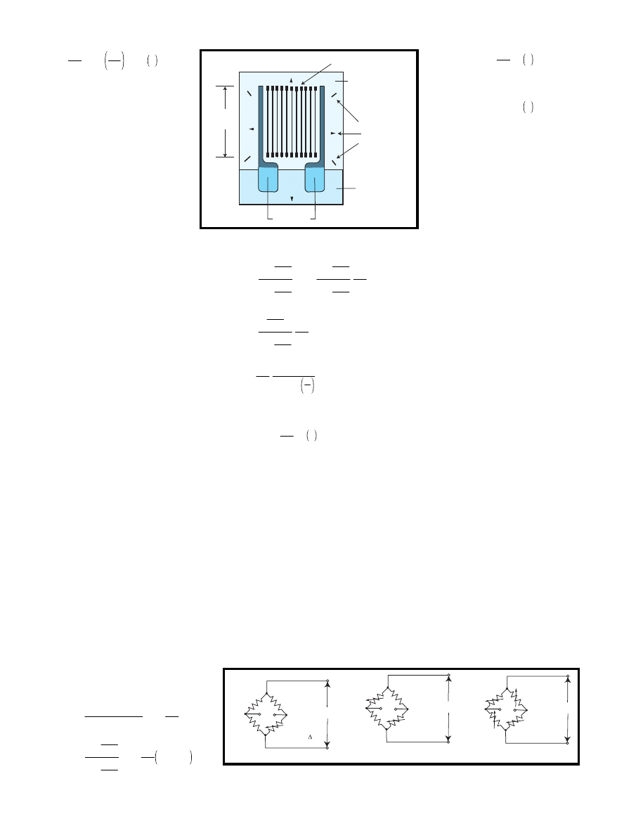
Modern strain gages are con-
figured as a metal foil grid that is
entirely bonded to the object
under test, as shown in Figure 1.
There are many variations of this
basic grid, in fact, too many to cover
here. Common values for R are 120,
350, 500, and 1000
W
. Because the
resistance change is usually small, it
can’t be accurately measured using
just a voltmeter.
A classic, time-proven solution is
the Wheatstone bridge, as shown in
Figures 2a, b, and c. Named after Sir
Charles Wheatstone, 1802–1875, the
Wheatstone bridge was actually in-
vented by Samuel Christie 10 years
earlier in 1833. A supply voltage:
Vin = (V+) – (V–)
is applied to the bridge consisting of
R1, R2, R3, and R4 (where R4 = Rg,
the gage resistance).
With little observation, it’s intui-
tive that if R1/R3 = R2/R4 then the
bridge will be balanced and Vb will be
0. Although they needn’t be, it’s com-
mon to have all four resistors equal to
one of the nominal values above when
no stress is present. For now, let’s
assume that this is the case.
Under an applied stress, Rg will
change by an amount
D
Rg
. The bridge
becomes unbalanced [1], and:
=
1 +
∆
R
g
R
g
2 +
∆
R
g
R
g
V
in
–
2 +
∆
R
g
R
g
2 +
∆
R
g
R
g
V
in
2
=
∆
R
g
R
g
2 +
∆
R
g
R
g
V
in
2
=
V
in
4
GF
(ε)
1 + GF
ε
2
so
V
b
≈
V
in
4
GF
ε
Since
Î
<< 1
This is known as a quarter-bridge,
because only one of the four resistors
changes, as shown in Figure 2a. Half-
and full-bridges are shown in Figures
2b and 2c, respectively. These bridges
assume that gages on opposite arms of
the bridge are under the same condi-
tions of stress (e.g., R1 and R4 of the
half-bridge are identical gages and
both are under the same tension or
the same compression). However,
there are many other circuit arrange-
ments, depending on the placement of
each gage [2], [3]. If we use the same
techniques that we used for the quar-
ter-bridge, we would get:
V
b
=
V
in
2
GF
ε
for the half-bridge and:
V
b
= V
in
GF
ε
for the full-bridge.
Even though the bridge circuit
gives a differential measure-
ment, Vb still needs amplifica-
tion so the final voltage can be
read by less expensive devices,
such as panel meters or the more
common ADCs. Figure 3 shows
the circuitry to amplify Vb as
well as potentiometers for set-
ting the span and offset for a
quarter bridge. The gain will be
N
multiplied by a fraction determined
by P2. V
AD
can now be connected to a
meter, converter, or a microcontrol-
ler. There are other ways to imple-
ment a bridge, but the above method
is straightforward and easy to analyze.
FEELING THE STRESS
One of the more difficult applica-
tions of strain gages is the strain sur-
vey, where many, possibly hundreds
of gages are measured under different
conditions of external loading. A good
example is the testing of aircraft. It’s
important to know the response of the
wings and fuselage, especially under
different conditions of applied stress.
A typical test uses several hydrau-
lic rams placed at strategic positions
as well as gages at areas where the
strain is expected to be significant.
The load-strain data is input to com-
puter programs that calculate a field
from the discrete measurements, thus
allowing the engineers to interpolate
or extrapolate the strain in other ar-
eas. Two of the better-known pro-
grams are NASTRAN and ANSYS,
which use the numerical technique of
finite-element analysis [5]. Modern
Figure 1
—Here’s a look at the typical construction of a modern foil-
grid strain gage.
Gage
length
Resistive grid
Alignment
marks
Bondable substrate
Solder tabs
Encapsulating
material
Figure 2
—When it comes to strain gages, you can have quarter bridges (a), half bridges (b), and full bridges (c).
–V
V
in
R
1
R
3
V
b
+V
R
4
= R
g
+ R
g
R
2
= R
g
V
in
R
1
R
3
V
b
R
4
R
2
V
in
R
1
R
3
V
b
R
4
R
2
a)
b)
c)
V
b
=
R
g
+
∆
R
g
R
2
+ R
g
+
∆
R
g
V
in
–
V
in
2
=
1 +
∆
R
g
R
g
2 +
∆
R
g
R
g
V
in
–
V
in
2
R
2
= R
g
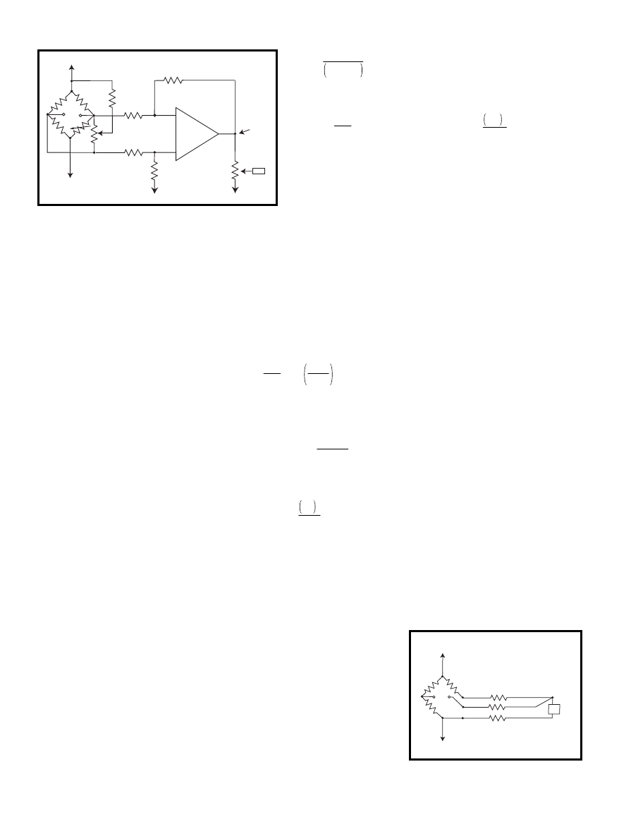
28
Issue 115 February 2000
CIRCUIT CELLAR
®
www.circuitcellar.com
PCs are so powerful that many analy-
sis programs are now available for the
desktop environment.
Such a test requires accurate data,
namely resistance changes in the
gages that are due only to strain.
There are many sources of potential
error, but the two most significant are
added resistance from long lead wires
and resistance changes as a result of
temperature variations of the gages.
Lead wire resistance is cancelled
using the method in Figure 4, a rather
ingenious scheme known as the three-
wire system. Still assuming equal
resistance in each bridge arm with no
applied stress, observe that point P of
the bridge (this junction is actually at
one of the gage’s solder tabs) will be
at a voltage of Vin/2 because:
R
2
+ R
L
= R
g
+ R
L
the third lead resistance goes to what-
ever instrument or circuit measures
Vb and has no effect on the balance of
the bridge.
A method for switching different
gages with long lead wires is shown in
Figure 5. In a manual system, S would
be a triple-throw X-pole switch,
where there are no more than X gages.
In systems with large numbers of
gages, banks of relays would switch
the gages based on address-decoding
circuitry, where the addresses are
generated by a PC or a
microcontroller.
This is all nice, but the lead-wire
resistance causes another problem.
The same change in resistance (
D
Rg
)
now causes the rest of the system to
see a percentage change of:
∆
R
g
R
g
+ R
l
instead of:
∆
R
g
R
g
The solution is to
use shunt calibration
resistors to produce a
known
D
Rg/Rg. These
resistors are jumpered
in parallel with a gage
at the gage’s solder
tabs to give a lower resistance than
the nominal. The gain of the system
is adjusted to read what it would have
read without the added lead resis-
tance. For example, with a 350-
W
strain gage and a gage factor of 2.0,
you might want to simulate a strain
of 5000 microstrain by a resistor (Rs)
in parallel:
∆
R
g
R
g
= 2.0 5000
10
6
= .01
∆
R
g
= 3.5
Ω
In general:
∆
R
g
= R
g
R
g
R
s
R
g
+ R
s
then:
R
s
=
R
g
2
∆
R
g
– R
g
For 5000 microstrain, Rs would
equal 34,650
W
. Similarly for 1000
microstrain, Rs would equal
174,650
W
. So, the best procedure
would be to connect 34,650
W
in par-
allel with the selected gage and adjust
the system’s gain so the final result is
a reading of –5000 microstrain. This
arrangement would indicate compres-
sion, since the resistance at the gage
has decreased.
BEATING THE HEAT
The other major cause of false
readings is temperature. Self-heating
effects depend on the current through
the gage and on the properties of the
material to which it is bonded. Limit-
ing the current through the bridge is a
necessity to avoid self-heating. For a
bridge with four arms, each of nomi-
nal resistance (Rg), the total power
dissipated will be:
V
in
2
R
g
and the power dissipated by a single
gage is one-fourth of this. So, if 5 V is
applied to a 350-
W
bridge, the power
in a single arm will be 18 mW. Dou-
bling the supply to 10 V will double
the bridge output for a given strain,
but it will quadruple the 18 mW to
72 mW. For this reason, you are better
off keeping the excitation low and
making use of good amplifiers to get
reasonable signals.
To minimize errors from thermal
resistance changes other than self-
heating, a basic method uses a second
strain gage that is subject to the same
temperature as the first. One way is
to use a dummy gage bonded to a
piece of the same material as in the
object to be tested. The dummy gage
is kept at the same temperature as the
object and is connected in an adjacent
arm of the bridge. Note here that
thermally induced resistance changes
will be the same in both arms, so they
will cancel and not contribute to
bridge unbalance.
The other technique is to take
advantage of the geometry of the ob-
ject. Figure 6a shows a cantilever
beam under an applied force (F). If
gages R4 and R2 are placed directly
opposite each other and along the long
axis of the beam, the positive resis-
tance change of R4 will be equal in
magnitude to the negative change of
R2
(assuming proper axial alignment).
Instead of using the circuitry in
Figure 3
—This is a common circuit for amplifying and zeroing the differential
voltage, Vb.
Figure 4
—The three-wire system cancels the effect of
long lead wires.
V
A
R
1
R
3
V
b
R
5
R
2
SPAN
NR
0
P
2
V
AD
R
0
R
0
NR
0
P
1
ZERO
R
4
= Rg
–V
+V
U
1
–
+
R
1
R
3
V
b
R
L
R
2
R
L
R
L
–V
+V
Rg
P
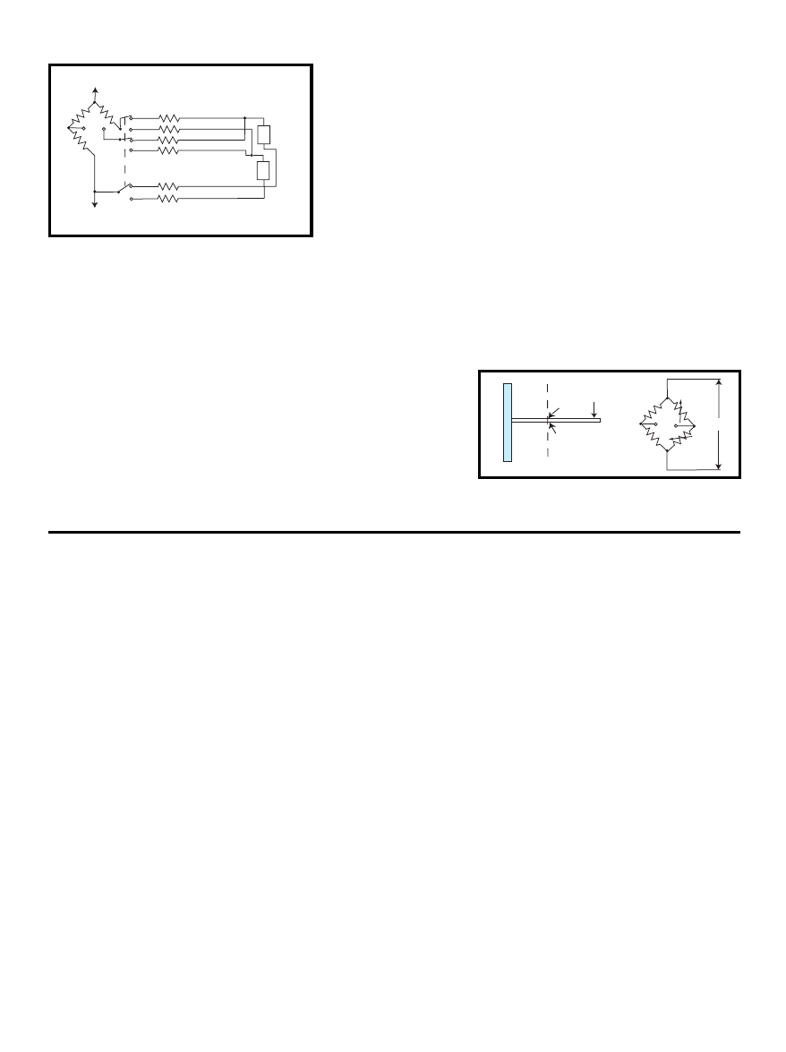
CIRCUIT CELLAR
®
Issue 115 February 2000
29
www.circuitcellar.com
Figure 2b, the gages are made into a
half-bridge as in Figure 6b. Now any
resistance changes due to temperature
will be of the same magnitude and
sign and will cancel, whereas the
strain-induced changes will add.
When these methods aren’t conve-
nient, the easiest overall solution is to
again take advantage of modern tech-
nology. Gage manufacturers have
developed metal alloys to the extent
that they are now available with tem-
perature coefficients of expansion that
are nearly the opposite of certain ma-
Figure 5
—Here you can see the result of switching multiple gages
when the gages have long lead wires.
terials [2], [3] (see Table 1 for
some common values).
CARRYING THE LOAD
Having covered all this
detail, you’re probably won-
dering how gages can be used
in everyday applications.
Well, this is actually where
strain gages find their greatest
utility. Today, load cells for
weighing and force measure-
ment, and pressure sensors for
monitoring industrial pro-
cesses are almost always made up of
strain gages and are specially config-
ured for given ranges and working
environments. Being made from full-
bridge connections, their out-
puts are relatively stable over
wide temperature ranges.
One type of load-cell geom-
etry (not necessarily the most
common) is shown in Figure
7a and an example of a pres-
sure transducer is shown in
Figure 7b. Note the similarity
in the tension and compression
areas and in the way they are sensed
by the bridge (refer back to the draw-
ing in Figure 2c). These two types of
transducers are definitely the work-
horses of the strain-gage family. Less
common are transducers such as
torque sensors, tension links, and
accelerometers [4].
There have been many approaches
and configurations over the years, and
the really solid designs have re-
mained. Others, such as accelero-
meters and certain low-pressure
sensors, have largely been displaced
by piezoelectric and semiconductor
sensors. For those interested, the
references listed offer the quickest
way to investigate these further.
R
1
R
3
V
b
R
2
–V
+V
R
La
R
La
R
Lb
R
Lb
R
Lb
R
La
P
1
R
g2
P
2
R
g1
S
1
R2
R4
F
R
1
R
3
V
b
R
2
R
4
V
in
a)
b)
Figure 6
—In this application of a cantilever beam with tension
and compression (a), the circuitry (b) cancels temperature effects.
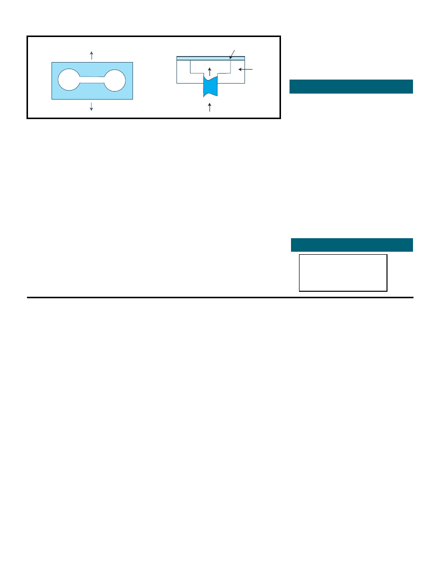
30
Issue 115 February 2000
CIRCUIT CELLAR
®
www.circuitcellar.com
REFERENCES
[1] Analog Devices, Inc., The
Transducer Interfacing Hand-
book
, 1980.
[2] The Measurements Group,
www.measurementsgroup.com/
guide/tn/tn505/505stc.htm.
[3] Omega Engineering, Pressure
and Strain Handbook
, 1998.
[4] C. Perry and H. Lissner, The
Strain Gage Primer
, McGraw-
Hill, New York, 1955.
[5] T.R. Chandrupatla and A.D.
Belegundu, Introduction to Finite
Elements in Engineering
, Prentice
Hall, Englewood Cliffs, NJ, 1996.
Dana Romero spent 13 years working
with sensors and their electronic
interfaces in an Air Force laboratory
and currently works at Phonex Broad-
band Corp. developing wireless prod-
R
1
R
3
R
2
R
4
F
Figure 7
—Two common types of transducers are the load-cell design (a) and the diaphragm pressure transducer (b).
a)
b)
R
1
R
2
R
3
R
4
Diaphragm
Body
Fluid inlet
IN GENERAL
What has been said about strain
gages applies also to other resistive
sensors, such as RTDs, thermistors,
and whatever others you may encoun-
ter. For all the detail and diversity of
the ideas that have been touched on,
they still fall into just one aspect of
the Wheatstone bridge. After all, it
was developed before the advent of
strain gages, and was intended to
measure differences in resistors using
a DC excitation voltage.
The bridge concept was expanded
to the measurement of impedances.
With the resistors replaced by general
impedances and the bridge supplied by
an AC source, you can measure small
changes in inductance and capaci-
tance. This idea appeared in the form
of R-L-C impedance bridges, which
can give accurate values when an
unknown impedance is compared to a
known one.
So, the next time you find yourself
faced with a measurement problem of
this sort, think Wheatstone bridge, and
don’t be afraid of the unfamiliar.
I
ucts for home telephony, modem
communications, and sound systems.
You may reach Dana at
dromero@phonex.com.
SOURCE
Omega Engineering, Inc.
(800) 826-6342
(203) 359-1660
www.omega.com
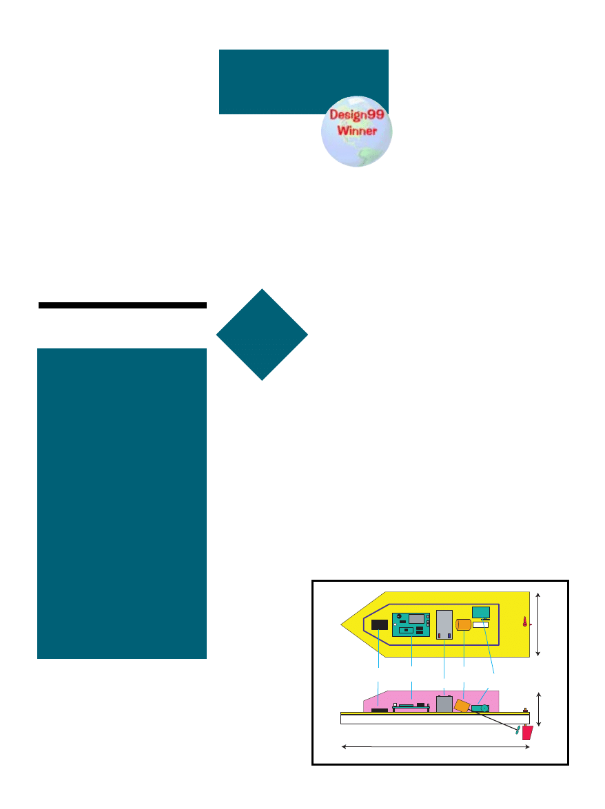
32
Issue 115 February 2000
CIRCUIT CELLAR
®
www.circuitcellar.com
Launching the Roboat
FEATURE
ARTICLE
Riccardo Rocca
t
Riccardo’s first-prize-
winning Design 99
project tests the feasi-
bility of an autono-
mous GPS-guided
model. Step aboard
for this stem-to-stern
review of everything
from the details of
construction to the
software required for
its maiden voyage.
his project aims
at testing the feasi-
bility of driving an
object using a GPS and a
digital compass. In this case, the ob-
ject is a model boat that can sail au-
tonomously along a course planned in
advance.
At the core of the Roboat is the
M68HC908GP20 (the quad flat plastic
pack version) controller that stores
the coordinates of the waypoints to
follow and, according to the data re-
ceived from the GPS and from the
digital compass, controls the electric
motor for the propeller and the pro-
portional servo for the rudder. Three
switches enable the test modes (dis-
abling the control of GPS and/or com-
pass), and a potentiometer allows you
to trim the rudder center position.
A MON08 interface allows the
connection with the ICS08GP20
board, in order to control the Roboat
directly from a PC for testing purpose
and when new waypoints need to be
stored.
A 12-V lead battery supplies power
to the devices. The electric motor of
the propeller is driven by 12-V di-
rectly, while the other circuits receive
a 5-V power supply through a suitable
regulator.
MECHANICAL ASSEMBLY
The structure of Roboat is simple,
so that it can be easily modified and
adapted. It is made of a sheet of poly-
styrene foam (4 cm thick) cut in the
shape of a boat with a thin sheet of
plastic on top, on which all the de-
vices (i.e., battery, electronics, elec-
tric motor, propeller, servo, and
rudder) are mounted, as you can see in
Figure 1. While sailing, all the devices
are covered with a case that protects
them from exposure to water.
The area chosen for the first
Roboat test was Lake Idroscalo, which
is close to Linate airport, 5 km east of
Milan, in northern Italy (see Figure 2).
It is an artificial lake, once used as a
“runway” for seaplanes. These days
the lake is primarily used by rowboats
and sailboats, which makes it rather
quiet, and thus safe for testing pur-
poses.
The test journey was about 1.5 km
and it is described by four waypoints
and their corresponding coordinates.
The coordinates of the four waypoints
Figure 1
—The Roboat
features a straightforward
design mounted on a
polystyrene foam board
platform.
Navigation by GPS and Digital Compass
80 cm
30 cm
10 cm
GPS
antenna
Electronic
board
Battery
Electric
motor
Proportional
servo
Rudder
Propeller
Top
view
Side
view
Protective
case
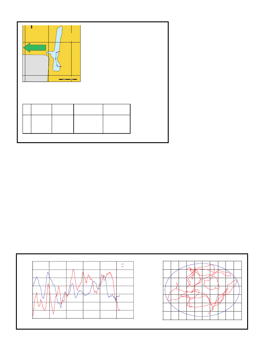
CIRCUIT CELLAR
®
Issue 115 February 2000
33
www.circuitcellar.com
45˚ 28'
45˚ 27'
9˚ 18'
9˚ 17'
9˚ 16'
Linate
Airport
MILANO
5 km
“Idroscalo”
lake
1
2
3
4
Start
North
Arrive
Longitude east of Greenwich
Latitude
north
1 km
Point
Longitude
Latitude
Long.
Lat.
Long.
Lat.
N.
deg
min
deg
min
dec
dec
hex
hex
1
9˚
17,3365
45 ˚
27,6986
5573365
27276986
550AF5 1A036BA
2
9˚
17,3135
45 ˚
27,4959
5573135
27274959
550A0F 1A02ECF
3
9˚
17,3750
45 ˚
27,2838
5573750
27272838
550C76
1A02686
4
9˚
17,4327
45 ˚
27,2635
5574327
27272635
550EB7 1A025BB
X & Y = (degrees × 60 + minutes) × 10000
Xcf = meters/minutes of longitude
= 1300 dec.
= 514 hex
Ycf = meters/minutes of latitude
= 1860 dec.
= 744 hex
are shown at the bottom of Figure 2.
They are expressed in:
• degrees, minutes, and decimals (GPS
NMEA format)
• integer decimals (to normalize de-
grees, minutes, and decimals into a
single number)
• integer hexadecimal numbers (to
store the coordinates, these are the
numbers that appear in the software
listing)
GPS
The accuracy of this method for
the basic, commercial GPSs, is said to
be within 100 m for the 99% of the
measurements collected in the same
place during an sufficient interval of
time. (For more information on GPS
and its accuracy, see the series of
articles by Ingo Cyliax in Circuit
Cellar
109–111.)
A test was done with the GPS
mounted on the Roboat. A number of
measurements were collected at the
same spot over a period of 50 min.,
and then plotted to obtain the dia-
grams shown in Figures 3a and b. As
you can see, the measurements actu-
ally fluctuate in time with periods of
roughly 5–10 min. and variations of
±
50–60 m.
These results confirm that the
degree of accuracy for this GPS is
actually in the order of tens of meters.
That information was taken into ac-
count when planning the course, so
the Roboat never approached any
obstacle (island or a shoreline) at a
distance closer than 100 m.
The GPS device used in the
projects is a Garmin GPS25-LVS with
the preamplified antenna GA27A. It
sends a string of ASCII data, according
to the NMEA format, through the
serial output once every second, at a
rate of 4800 bps (see Figure 4).
The string is terminated by the
ASCII codes “13” (carriage return) and
“10” (line feed). Once a string is re-
ceived, it is checked for reliability by
testing the checksum byte and by
verifying that the acquisition code is
“A”.
The data that the program actually
reads and uses are the latitude and the
longitude. Both latitude and longitude
are output by the GPS in the form of
degrees, minutes, and fractions of
minutes, therefore the program first
converts them into “deci-milli-min-
utes of degree,” in order to obtain a
single integer number, without the
troubles associated with degrees,
minutes, and fractions of minutes.
This process is accomplished using
the formulas:
latitude = (dd × 60 + MM.mmnn) ×
10000
longitude = (Ddd × 60 + MM.mmnn) ×
10000
In assembler, the formulas are
actually split into smaller bits be-
cause the strings of ASCII data are
first converted into binary bytes (two
Figure 2
—The Idroscalo lake test site was
chosen for its low volume of traffic and the
absence of motor craft, which would cause
wakes that complicate test-course naviga-
tion. The designated waypoints are defined
in the table.
-70
-50
-30
-10
10
30
50
70
0
10
20
30
40
50
60
time (minutes)
swing (meters)
N-S
E-W
-80
-60
-40
-20
0
20
40
60
-50
-40
-30
-20
-10
0
10
20
30
40
50
E-W swing (meters)
N-S swing (meters)
Figure 3a
—GPS accuracy wanders slightly more than expected when plotted against time of day. b—Position variances are also to be expected.
a)
b)
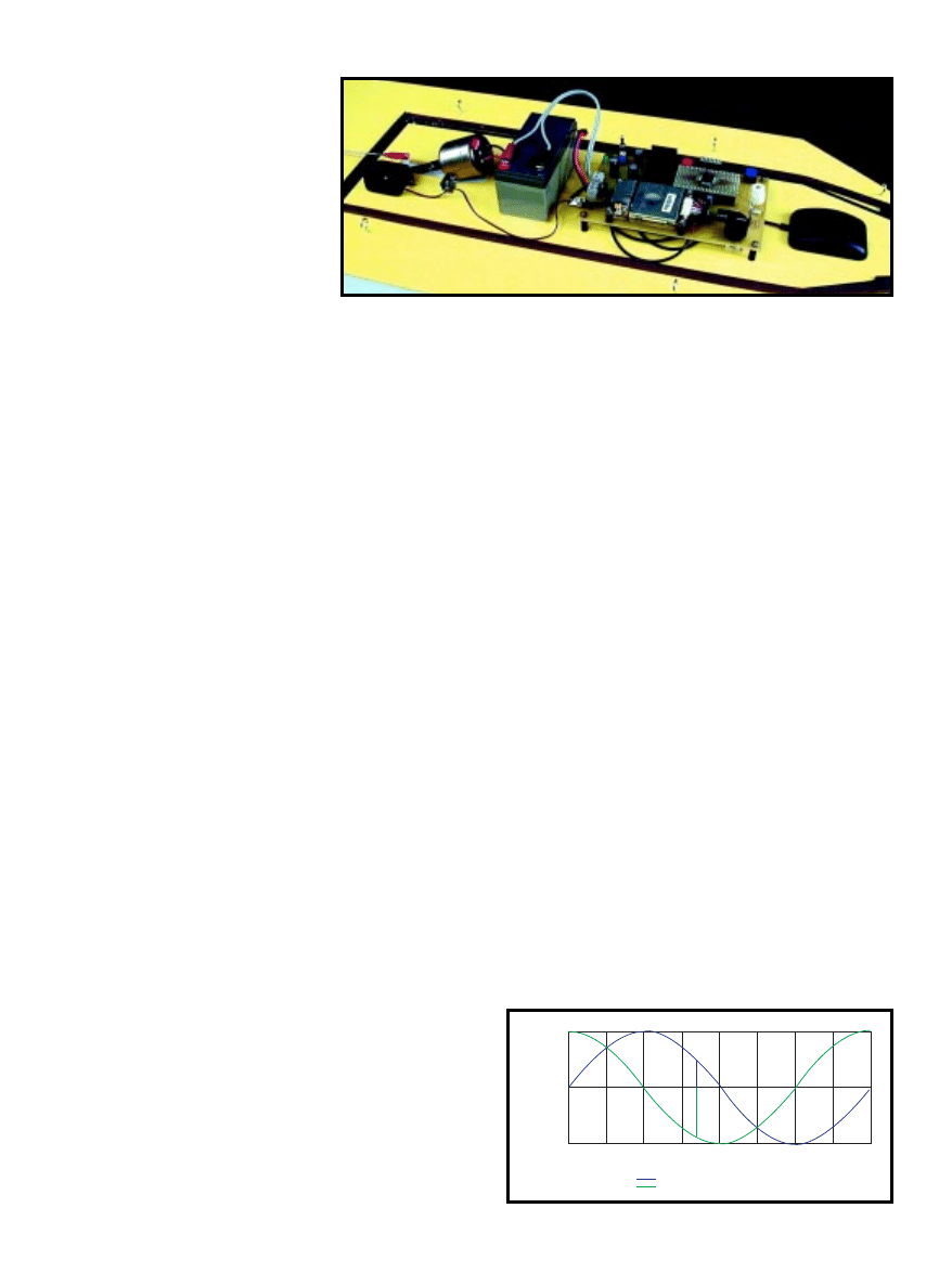
34
Issue 115 February 2000
CIRCUIT CELLAR
®
www.circuitcellar.com
characters at a time). Therefore, the
actual formulas are:
latitude = ((dd × 60 + MM) × 100 +
mm) × 100 + nn
longitude = (((D × 100 + dd) × 60 +
MM) × 100 + mm) × 100 + nn
The coordinates of the GPS are
then compared to the coordinates of
the next course point, and the linear
distances to it are calculated ex-
pressed in meters, such as:
dX = |longitude – course_point_long| ×
Xcf/10000
dY = |latitude – course_point_lat| ×
Ycf/10000
Xcf and Ycf are the conversion
factors and should be chosen accord-
ing to the geographical area where the
Roboat is going to sail. The factors are
computed as:
Xcf = meters/minutes of longitude
($512 in the test area shown in
Figure 2)
Ycf = meters / minutes of latitude
($744 in the test area)
There is no checking done for east
or west longitude, or for north or
south latitude, so the rest of the
Roboat program works properly only
with positive longitudes and latitudes
(as in most parts of Europe, Asia, and
North Africa).
DIGITAL COMPASS
The Roboat uses a digital compass
sensor analog model 6100 (distributed
by Pewatron) to determine which
direction the Roboat is heading (azi-
muth). This sensor has the shape of a
small cylinder that is 15 mm high and
13 mm in diameter, and contains a
tiny magnet and two Hall-effect sen-
sors. The magnet is free to rotate
around its vertical axis and point
north under the influence of the
earth’s magnetic field.
The two Hall-effect sensors are
mounted around the tiny magnet, 90°
apart from each other. When the
magnet rotates, the outputs of the
two sensors describe the sine and
cosine curves that, using a power
supply of 5 V, have an average value
of 2.5 V and range between 1.8 and
3.2 V.
The Roboat azimuth (degreed) can
then be computed as the ArcTangent
of the ratio of the displacements of
the two curves from the average (see
Figure 4).
Figure 4
—The Roboat
determines its location from
the ArcTangent of the ratio of
the displacements of the two
curves shown here.
1.80
2.50
3.20
0
45
90
135
180
225
270
315
360
Azimuth
(degrees)
Output voltage
Dcosine
Dsine
sine
cosine
Azimuth = ArcTangent (Dsine / Dcosine)
North
East
South
West
North
Photo 1
—The GPS and antenna are situated far forward, ahead of the circuit board and power plant. A 12-V battery
powers the motor and electronics.
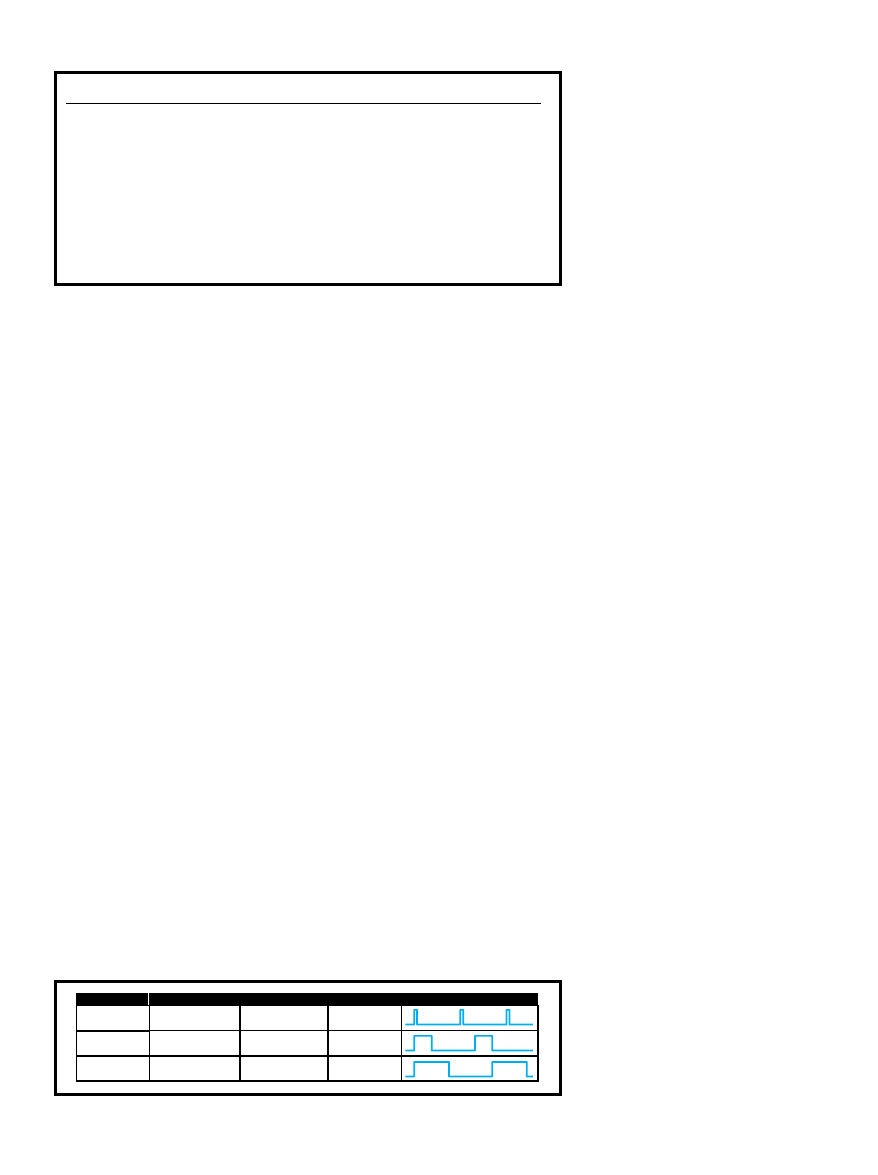
CIRCUIT CELLAR
®
Issue 115 February 2000
35
www.circuitcellar.com
Pin
Function
PTA1
SW5 disables GPS course updates (Roboat test mode)
PTA2
SW4 disables compass course updates (Roboat test mode)
PTA3
SW3 copies the present compass course into the GPS course (Roboat test mode)
PTB0
analog input from the trimmer that adjusts the central position of the rudder
PTB1
analog input from the digital compass Hall sensor 1
PTB2
analog input from the digital compass Hall sensor 2
PTC2
output, switches the electric motor and propeller (1 = off, 0 = on)
PTC4
output, powers down the GPS (1 = off, 0 = on)
PTD4
output, controls the proportional servo and rudder
PTD6
output, blinks the red LED each time correct data from GPS are acquired
PTE1
input, receives serial data from GPS
PROPORTIONAL SERVO
The rudder is controlled by a pro-
portional servo of the same type used
in radio controls for models. The
servo wheel turns under control of a
periodic positive pulse and the
amount of rotation (±90°) of the
wheel is proportional to the pulse
width (see Figure 5).
The pulse is generated at pin 4 of
Port D, under control of Timer 1,
which is set in a PWM-buffered mode.
In this mode, the pulse width is under
control of Timer 1, Channel 0, and
Channel 1, alternatly. While one
channel controls the pulse, the other
channel can be updated. The change
will appear in the next pulse only, so
there is no danger of applying undes-
ired changes in the middle of a pulse.
The alternating selection of chan-
nels is done automatically by the
hardware. The software uses bit 1 of
register T1SC1 as a flag bit. The bit
toggles at every overflow of T1SC0
and its value indicates which channel
is to be written next.
The unconventional use of T1SC1 is
possible because the register isn’t used
in buffered PWM mode. It is T1SC0 that
controls both channel registers.
CIRCUIT DESCRIPTION
The electronic circuit receives
power from the 12-V battery through
Figure 5
—The control pulse geometry for extremes in rudder postion drives the sailing direction of the Roboat.
the main switch SW1. When SW1 is
on, the green LED (D1) lights to show
that the power is on.
Twelve volts are applied directly to
the electric motor, under control of
IC4-PTC2, through the buffer IC3f
and the electronic switch TR1. C11
helps reduce the noise generated by
the motor when in use.
The rest of the circuit is powered
with 5 V through the voltage regula-
tors IC1–C2 and IC2–C3. The reason
for using two identical regulators is to
isolate the servo so the noise spikes
that it generates are not passed to the
rest of the circuit. So, IC2 powers just
the servo and IC1 powers the rest of
the circuit.
The M68HC908GP20 (IC4) is the
core of the circuit. The Roboat’s con-
troller works with a frequency of
4.9152 MHz generated by the oscilla-
tor X1, IC3a, R3, C7, C8.
C4 and C5 are mounted close to
the power-supply pins VDD and
VDDA, to prevent noise problems. A
stronger filter for the pin VDDAD is
provided by R4 and C6, in order to
prevent noise that might affect the
A/D conversion.
SW2 and C7 provide the manual
reset to IC4. The pins IRQ, RST,
PTA0,7, and PTC0,1,3 of IC4 are con-
nected to the MON08 connector,
which provides a link (via a 16-wire
Servo wheel rotation
Pulse width (ms)
Value in Timer 1
Control signal
-90˚
0.2
$0200
central position
1.25
$0C00
+90˚
2.3
$1600
Rudder position
Full left
Center
Full Right
Table 1
—Here’s a look at the pin assignments for the M68HC908GP20 onboard the Roboat. Serial GPS data for
heading calculations is on PTE1.

36
Issue 115 February 2000
CIRCUIT CELLAR
®
www.circuitcellar.com
flat cable) with the ICS08GP20
board. This arrangement enabled me
to control the Roboat directly from a
PC for testing purposes and whenever
new waypoint coordinates need to be
loaded.
When the link isn’t in use (i.e.,
when the Roboat is sailing autono-
mously), a proper socket must be
fitted to the connector instead of the
flat cable. IC4-PTD4 pin generates the
PWM signal that controls the servo
and is connected to the control input
of the servo through the buffer IC3b.
The IC4-PTE1 pin receives the
serial signal from the GPS after the
signal is inverted by IC3d. IC4-PTC4
pin controls the GPS powerdown
mode through the buffer IC3e. IC4-
PTD6 controls the red LED (D2)
through the buffer IC3c and lets it
flash every time the GPS receives a
valid position.
The digital compass analog out-
puts, as well as R8 (the trimmer for
centering the rudder), are connected
to the A/D converter inputs of IC4
(pins AD0, AD1, AD2)
through the low-pass fil-
ters R5-C10, R6-C11,
R7-C12.
The construction of the
PCB has some peculiari-
ties. First off, IC4 is
mounted on a custom
socket that converts the
44-pin QFP geometry into
a 22 + 22 pin DIL, with the
more practical pin spacing
distance of 0.1
²
.
The socket is built with
a small PCB (32 × 57 mm),
single sided, with the
copper traces facing up-
wards. IC4 is soldered on
top of the PCB and two
rows of 22 pins are sol-
dered at its sides, facing
downwards. This assembly
is mounted on the main
PCB, in the two rows of 22
+ 22 SIL sockets.
The GPS is mounted on
the PCB main board with
four screws, bolts, and
spacers. The GPS standard
output is made of 12 indi-
vidual wires, only 10 of
which are actually used. To obtain a
cleaner assembly, the 10 wires were
assembled into a 5 + 5 flat-cable
socket. The socket is finally con-
nected with the 10-pin connector (K4)
on the main PCB.
The soldering instructions pro-
vided with the digital compass warn
to take special care in soldering the
device, because overheating will
damage the sensor. To avoid any risk,
the digital compass used in this
project was not soldered, but rather it
was mounted into a couple of 3 + 3
SIL sockets previously soldered in
the main PCB.
When the Roboat works
autonomously and isn’t
linked to the ICS08GP20
board, suitable jumpers
must be fitted on the
MON08 connector instead
of the flat-cable connector.
This is more easily accom-
plished by a double row of
16-way sockets soldered on
a tiny PCB 20 × 5 mm.
The potentiometer R8 is fixed to
the PCB with washers and its termi-
nals are soldered directly to the PCB
copper tracks.
SOFTWARE
The main actions handled by the
Roboat’s software are:
• start the propeller and the GPS
• acquire data from the GPS and the
digital compass
• compute present course and position
• compute any course corrections
needed to reach the next waypoint
• apply any course corrections to the
rudder
• stop the propeller, GPS, and the
controller when the last waypoint is
reached
The main devices controlled by the
software are the GPS and aerial GA27,
the digital compass sensor analog,
proportional servo, and the 12-V elec-
tric motor. Table 1 shows the pin
assignments of the ’GP20CFB.
The flow chart in Figure 6 de-
scribes the program that runs in the
’GP20CFB and controls the devices.
After initialization, the program is
basically a continuous loop that is
periodically interrupted by four rou-
tines that control data acquisition
from the GPS (IntSCI), data acquisi-
tion from the digital compass
(IntADC), PWM pulse to the propor-
tional servo (IntTIM1), and the status
of SW3 (IntKBD).
TEST MODES
Test modes are controlled by SW3,
SW4, and SW5. When SW5 is closed,
data from the GPS is disabled, thus
the Roboat sails under control of the
digital compass only. Pushing SW3
Figure 6
—The program for piloting the Roboat makes use of stored
ADC values for the two digital compass sensors and the rudder trigger.
Initialize: SCI (to receive CGS messages)
DAC (to read digital compass & rudder trimmer)
Timer 1 (to control the rudder servo with PWM)
Timer 2 (to blink the red LED)
PORT-A (to acknowledge comtrol switches)
PORT-C (to switch the propeller on)
Loop waiting for interrupts:
- if (course point = last one) stop the propeller
power down the GPS
stop the processor
Serial communications interface interrupt:
- read the GPS
- if reading is reliable:
- blink the red LED
- reakon the planned course
- update the planned course if SW5 enables to do so
- reakon the distance to the next waypoint
- if (distance < close_dist) select further waypoint
Timer1 interrupt:
- read the digital compass values
- reckon the present Roboat course
- update the Roboat course if SW4 enables to do so
- reckon the difference between planned and present course
- set new PWM pulse according to the rudder trimmer
- adjust the PWM pulse according to courses difference
- apply the new PWM cycle to the rudder servo
Analog-to-digital converter interrupt:
- read sequencially at each new interrupt the ADC value from:
- rudder trigger
- digital compass Hall sensor 1
- digital compass Hall sensor 2
and store them in memory (ADC0, ADC1, ADC2)
Keyboard interrupt (from SW3) :
- copy the compass course into the GPS course
Table 2
—The ArcTangent computation formulas for the various compass
sectors become navigation data.
Keyword
Sector
ArcTangent formula
001
$00 – $20
$00 + $20 × DX/DY
000
$20 – $40
$40 – $20 × DY/DX
010
$40 – $60
$40 + $20 × DY/DX
011
$60 – $80
$80 – $20 × DX/DY
111
$80 – $A0
$80 + $20 × DX/DY
110
$A0 – $C0
$C0 – $20 × DY/DX
100
$C0 – $E0
$C0 + $20 × DY/DX
101
$E0 – $00
$00 – $20 × DX/DY
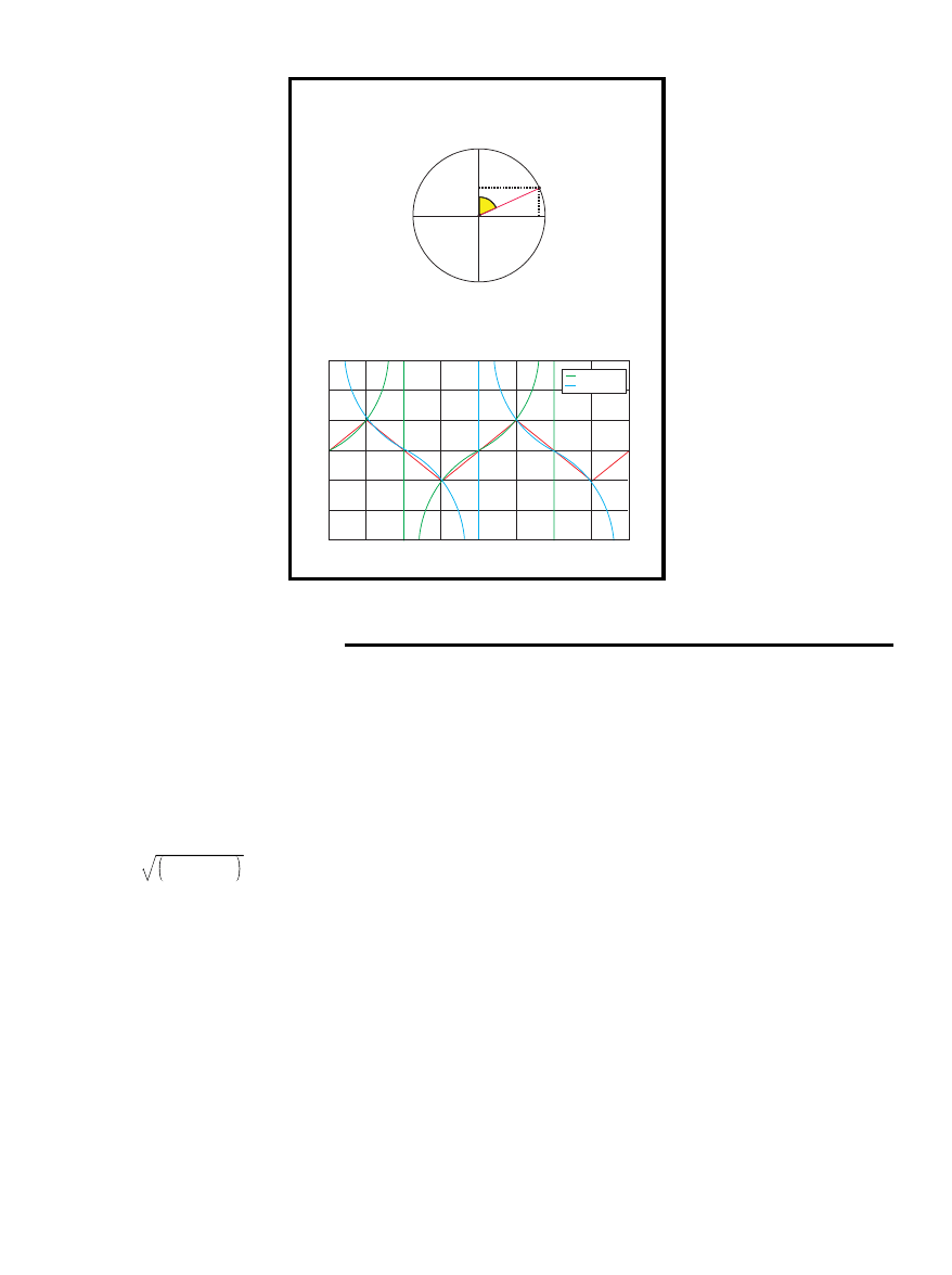
CIRCUIT CELLAR
®
Issue 115 February 2000
37
www.circuitcellar.com
–3
–2
–1
0
1
2
3
0
32
64
96
128
160
192
224
256
00
20
40
60
80
A0
C0
E0
00
DX
DY
North
South
West
East
$00
$20
$40
$60
$80
$A0
$C0
$E0
X0,Y0
X1,Y1
Cotangent
Tangent
stores the direction the
Roboat is presently heading
to as the reference course so
the Roboat will sail straight
along a fixed direction. This
is how the compass is tested.
When SW4 is closed, the
compass is disabled, which
allows the rudder to be con-
trolled by only the potenti-
ometer (R8) and thus it can
be adjusted for the Roboat to
sail straight.
Because the Roboat soft-
ware was written directly in
assembler, all the needed
mathematics deals with inte-
gers only. Latitude and longi-
tude data need four-byte
integers to be wholly repre-
sented. A few basic opera-
tions were developed to deal
with such long numbers, in
the form of the subroutines:
COMPAB, SWAPAB, ADDAB,
SUBAB, MULAB, and DIVAB.
These subroutines are a de-
velopment of the basic as-
sembler commands (cmp,
mov, add, sub, mul, div) and refer to
the four byte registers REGA, REGB,
REGC and REGD.
The subroutine
DIST compares the
distance to the next waypoint (located
at the coordinates DX,DY) with a
reference distance (RANGE), to define
if the waypoint is close enough to be
considered reached.
The formula for distances is:
DX
2
+ DY
2
But, to avoid dealing with square
roots, and because we only want to
compare distances, DX
2
+ DY
2
is com-
puted without the square root and
RANGE is squared instead. The for-
mula used in DIST then becomes (DX
× DX) + (DY × DY) compared to
(RANGE × RANGE).
More discussion is in order for
ATAN operation, which computes the
ArcTangent of the ratio DX/DY.
First of all, azimuths are repre-
sented with a one-byte value, that
indicates: North=$00, East=$40,
South=$80, West=$C0, as shown in
Figure 7a.
Figure 7a
—Azimuths are defined with a one-byte value. b—Here are the
approximations of tangent and cotangent values for navigation.
a)
b)
In order to work with inte-
gers only, the curves of the
tangent and cotangent func-
tions are approximated to a
sequence of straight segments
that describe the functions
quite closely in the range –1,
0, and +1 (see the solid red
line in Figure 7b).
The program works on the
coordinates of two points
(X0,Y0) and (X1,Y1), and
starts determining the sector
that contains the direction
(X0,Y0) -> (X1,Y1), by setting
the following flags:
if (X0>=X1) then (flag2=0) else
(flag2=1)
if (Y0>=Y1) then (flag1=0) else
(flag1=1)
if (DX>=DY) then (flag0=0)
else (flag0=1)
The value of flag2, 1, or 0
is entered in Table 2, the
corresponding keyword is
found and the appropriate
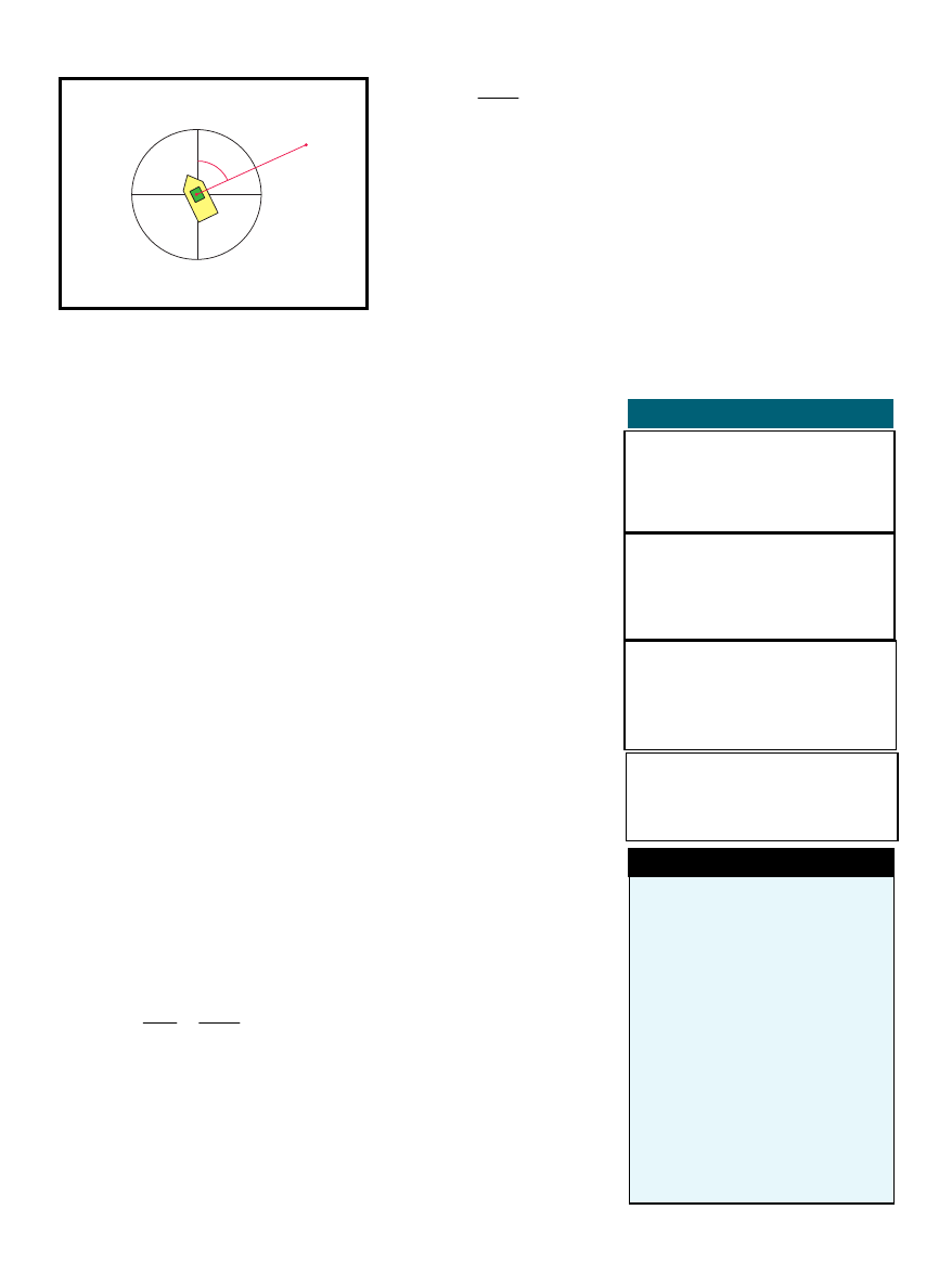
38
Issue 115 February 2000
CIRCUIT CELLAR
®
www.circuitcellar.com
SOURCES
GPS25, GA27
Garmin International, Inc.
(913) 397-8200
Fax: (913) 397-8282
www.garmin.com
6100 digital compass sensor analog
Pewatron AG
+41-1-830-2944
Fax: +41-1-830-5157
www.pewatron.com
MC68HC908GP20CFB
Motorola
(512) 328-2268
Fax: (512) 891-4465
www.mot-sps.com
Proportional servo
Futaba Corp. of America
(847) 884-1444
www.futaba.com
formula is selected to finally compute
the value of ArcTangent.
Another operation that deals with
simplified trigonometry is the compu-
tation of adjustments for the rudder
(see Figure 8). The program compares
two azimuths (the GPS course in the
direction of the next waypoint to be
reached and the compass course in the
direction where the Roboat is actually
heading) and then computes the new
position for the rudder inorder to steer
from the present heading towards the
next waypoint.
The position of the rudder is con-
trolled by the length of the pulse that
controls the proportional servo. This
value is computed starting from a
reference value (rudder_trim) that is
given by the rudder trimmer (R8).
The reference value can be adjusted
to set the rudder in the central posi-
tion and it can vary between $0500
and $1100 (±45° rotation of the servo
wheel).
Then (course_diff) is computed as
the absolute value of (GPS_course –
compass_course). This difference sets
the amount of rudder steering left or
right. Until the difference between
the two azimuths is small, as in:
45
+ 45
or
$20
+$20
the rudder steering is controlled pro-
portionally. At the difference value of
–$20 or +$20, the rudder reaches its
full right or left position and can’t
turn any further so the software con-
strains the difference value. When the
difference value increases outside the
range of:
Riccardo Rocca is a Senior Geophysi-
cist with an oil company in Italy. He
honed his skills in electronics while
experimenting in his home labora-
tory. Riccardo particularly enjoys
applying hardware and software in
the development of autonomous mo-
bile microrobots. A detailed descrip-
tion of his work is available at http://
users.iol.it/riccardo.rocca. You may
reach him at riccardo.rocca@ioil.it
Figure 8
—Course computation takes place based on readings
from the compass sensors and the retrieved GPS data, resulting
in a new steering value for approaching the next waypoint.
North
South
West
East
$00
$20
$40
$60
$80
$A0
$C0
$E0
GPS
course
course
Next
waypoint
Compass
$20
+$20
the software simply cuts it to
one edge of the range of +/–$20.
The final formula depends
on the comparison between the
GPS course and the compass
course:
if (GPS_course >
compass_course) then:
pulse_length = rudder_trim -
(course_diff × $28)
if (GPS_course <
compass_course) then:
pulse_length = rudder_trim +
(course_diff × $28)
For example, consider Figure 8
where:
compass_course = $F0
GPS_course = $30
course_diff = | GPS_course –
compass_course | = $40 and is fi-
nally cut to $20
Consider rudder_trim set at the
middle value = $0C00, then the for-
mula becomes:
pulse_length = $0C00 + ($20 × $28)
= $1100
This pulse value turns the rudder
completely to the right, so the Roboat
also starts steering right, thus heading
towards the next waypoint.
CROSSING THE ATLANTIC
After all the testing and a success-
ful maiden voyage on Lake Idroscalo,
the Roboat was ready for a bigger
journey. Actually, the Roboat’s trip
across the Atlantic had more to do
with being chosen as a Design99 con-
test winner. The only additional hard-
ware required for the trans-Atlantic
voyage was some well-placed card-
board and lots of styrofoam packing
material and then it was off to Circuit
Cellar
headquarters to be photo-
graphed.
As you can see in Photo 1, the trip
was successful. Although the Roboat’s
Atlantic voyage was made via airmail,
combining GPS and digital compass
technology with parts such as the
Motorola M68HC908GP20 can pro-
vide a world of opportunity when it
comes to design projects.
I
If you missed out on Design99,
there’s not much we can do now—
except tell you about the current
Circuit Cellar contest, Design2K!
Just build an innovative and high-
quality project using the Philips
51LPC family of 80C51-based
microcontrollers and you could win
$5000, a Sony VAIO laptop com-
puter, or a Philips PC external CD-
rewritable kit. The deadline is May 15
so visit our homepage for the details
and get started on your entry today.
Hopefully, we’ll be reading an
article about your award-winning
project next year!
DON’T MISS THE BOAT!

40
Issue 115 February 2000
CIRCUIT CELLAR
®
www.circuitcellar.com
Save Your Voice
FEATURE
ARTICLE
Duane Perkins
t
Tired of repeating
yourself? With
Duane’s project, you
won’t have to worry
about that because
he uses a PIC16C73
to make a sound
board for your PC.
Now you can record
speech and music
signals with almost
radio quality.
here are many
possible uses for a
voice-messaging sys-
tem. Announcements in
public facilities could provide blind
users with instructions or informa-
tion. Message files could be com-
pressed and sent to a recipient with a
sound board and passages in the mes-
sage could be frozen and displayed on
an oscilloscope for analysis of voice
characteristics.
In this article I explain how to
build a sound board that can record
and play back voice messages on a PC.
The sound board connects to the PC
via a bidirectional parallel port. A
PIC16C73 does the A/D conversion
and a DAC0801 chip does the D/A
conversion. A DTMF decoder detects
touch-tone signals when recording
from a telephone line.
Figure 1 shows the basic layout of
the sound board. The PIC16C73 uses
a 20-MHz crystal for the clock oscilla-
tor. Of the various pins connected to
the parallel port through J2, some are
inputs for status signals and some are
outputs that send control signals.
As you can see in Figure 2, there
are three 8-bit 74LS373 latches. U3 is
the input latch, U4 is the output
latch, and U5 is the DAC latch.
The PC controls the sound system
functions by way of three control-
register bits, SELIN, INIT and
AUTOFD (all active low). The port
must be truly bidirectional, with the
direction controlled by a bit in the
control register. I used a PIOC from
B&B Electronics.
When recording, the ACK line is
pulsed to send a byte. The PC pulses
the STROBE line as soon as the byte
is received. When playing, the PC
pulses the STROBE line to send a byte
and the PIC16C73 pulses the ACK
line when the byte is received.
The exchange is similar to a game
of table tennis. Each player reacts
when the ball is on his side. The
PIC16C73 and the PC both use FIFO
buffers to hold the data waiting to be
acted on. This setup allows asynchro-
nous data transfer while ADC or DAC
occurs at a 19,531-Hz sample rate.
Table 1 shows the setting of the
PC’s control register for the pro-
grammed functions. When set to AB
(SAFE), all data lines are hi-Z and all
control lines are low, assuring no
current flow if the board isn’t pow-
ered. These settings remain at all
times, except when the PC is running
a program that communicates with
the sound board.
To record, SELIN and INIT are
inactive (high) and AUTOFD is active
(low). Accordingly, PLAY (RC2) is
low, the output of U4 is on the I/O
bus, and the output of U3 is tristated
(hi-Z). The PIC samples and converts
the audio input at 51.2-µs intervals.
A Digital Sound Board
Table 1
—Here are some of the
settings of the parallel port’s
control register for the pro-
grammed functions. You can see
the state of the control lines and
whether interrupts are enabled.
Function HEX
SELIN
INIT
AUTOFD
PLAY
IRQ
Record
B6
H
H
L
L
Y
Play
1C
L
H
H
H
Y
Test
A4
H
H
H
L
N
Stop
AA
L
L
L
H
N
Pause
A6
H
H
L
L
N
Safe
AB
L
L
L
H
N
N/A
A0
H
L
H
H
N
N/A
0C
L
H
H
H
N
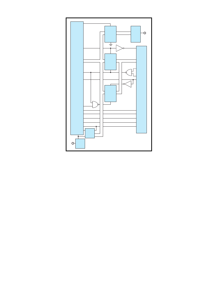
CIRCUIT CELLAR
®
Issue 115 February 2000
41
www.circuitcellar.com
PC that the data is a touch-
tone code. It waits 51.2 µs
before it tests T0IF and
_AUTOFD.
If T0IF or _AUTOFD is
clear, it pulses the ACK line
again, and continues until
TOIF and _AUTOFD are both
high (or the watchdog timer
times out). The PC captures
the data, verifies that the
high-order four bits are the
complement of the low-order
four bits, sets _AUTOFD low
and STROBE high, then waits
for _ERROR to go high. If the
data does not verify, the PC
simply sets the STROBE line
low while leaving _AUTOFD
high, thereby telling the
PIC16C73 to try again.
THE SOUND BOARD
The sound board has four
connectors. There’s an 8-pin
PCB connector block for
power, audio input, and the
level-control potentiometer, a
26-pin header for the parallel
port, a 3-pin header for a jump-
er or a connector to a switch,
and a 2-pin PCB connector for
audio output.
U7 (a TL082 dual op-amp)
is connected as an amplifier for re-
cording. It’s designed to accept a 300-
W
dynamic microphone, but a 600-
W
microphone can be used (R2 should be
changed to 560
W
).
The circuit has a variable gain
amplifier controlled by R1, followed
by a lowpass amplifier with a gain of
11 rolling off at 6 dB per octave start-
ing at about 3 kHz. Higher frequency
components that would not be cleanly
converted at the sampling frequency
are attenuated.
J3 can be jumpered for microphone
(upper two pins) or line input (lower
two pins). Line input should not ex-
ceed 160 mV RMS. The output is
coupled to a voltage divider (R12 and
R13), biasing the line to 2.5 V, which
is coupled to RA0 through R14 so the
source impedance is not lower than
Microchip specs. RA0 is protected by
diodes to Vdd and Vss and will clip the
audio signal if it exceeds either.
As long as the FIFO buffer
is empty, the ACK line is
pulsed, latching the ADC
result in U4. The PC captures
the data and stores it in its
FIFO buffer, then sends a
strobe pulse. If the PIC doesn’t
receive the strobe pulse
within 51.2 µs, it stores the
ADC result in its FIFO buffer.
When the strobe pulse is
received, the PIC retrieves the
earliest result from its FIFO
buffer, and latches it in U4 by
pulsing the ACK line. If the
PC is fast enough to receive
two bytes within 51.2 µs, it
will eventually empty the
FIFO buffer in the PIC. When
the buffer in the PC is more
than half full, the full half of
the buffer is written to the
hard drive.
To play a recorded voice
message, SELIN is active (low)
while INIT and AUTOFD are
inactive (high). The result is
that the output of U3 is put on
the data bus under the control
of the RECV pin (RC1) and the
output of U4 is tristated.
The PC starts by filling its
FIFO buffer before beginning
to send, and refills each half of
the buffer when it’s exhausted. After
storing the first byte in the data regis-
ter, it pulses the STROBE line, latch-
ing the data in U3. The PIC reads the
data, stores it in its FIFO buffer, and
pulses the ACK line. The PC sends
the next byte as soon as it can and the
exchange continues, with pauses
when the buffer in the PIC is full.
At 51.2-µs intervals, the PIC re-
trieves the next byte in its buffer and
latches it in U5. When the FIFO
buffer in the PC is less than half full,
it reads from the hard drive and fills
the half that is empty.
If SELIN, INIT, and AUTOFD are
inactive (all high), the ADC result is
latched in U5 and the DAC0801 con-
verts it back to analog. The audio
signal is amplified and passed to the
output. This process is useful for
testing and adjusting the gain. If
SELIN, INIT, and AUTOFD are active
(all low) the system idles.
The SELECT, _ERROR, PAPER,
and BUSY lines are controlled by the
PIC. SELECT is normally inactive
(low) but can be brought high by RA2.
_ERROR is normally inactive (high).
The PC can detect that the PIC
isn’t ready if _ERROR is low, which is
the case if the board isn’t powered.
BUSY and PAPER are used as flags by
the PIC, and can be used by the PC to
detect the current state of the PIC.
Touch-tone signals are decoded by
U8. When a valid tone pair is de-
tected, StD drives RA3 high. While
recording, the PIC and the PC verify
that the correct code is transferred,
repeating the exchange until it’s all
correct (error checking and correction).
The ’16C73 captures the data (low-
order four bits) and sets the high-order
four bits to the complement of the
low-order four bits, asserts _ERROR,
then pulses the ACK line, thus latch-
ing the data in U4 and signaling the
RC5
U1
Sound
PIC17C73A
Ack
RC4
Port B
RC2
Data bus
Play
RA4
Strobe
U5
Sound bus
U6
DA0801
Audio
out
RC4
ACK
Ack
E
D
Q
74LS373
*OC
U3
E
D
Q
74LS373
*OC
U4
U2C
U2A
10
17
16
J2
U2B
U2D
Data
I/O bus
1
15
14
12
11
13
SELIN
INIT
Strobe
E
D
Q
74LS373
*OC
RC1
RC0
RC6
RC7
RC3
RA2
RA5
RA0
RECV
*ERROR
*AUTOFD
Paper
Busy
Select
Error
AUTOFD
Paper
Busy
Select
DTMF
Decoder
Audio
in
Amp
Out
In
U5
Figure 1
—The sound board connects to the parallel port’s data, status, and
control lines via J2. The PC controls the sound board by setting the control
register as shown in Table 1.
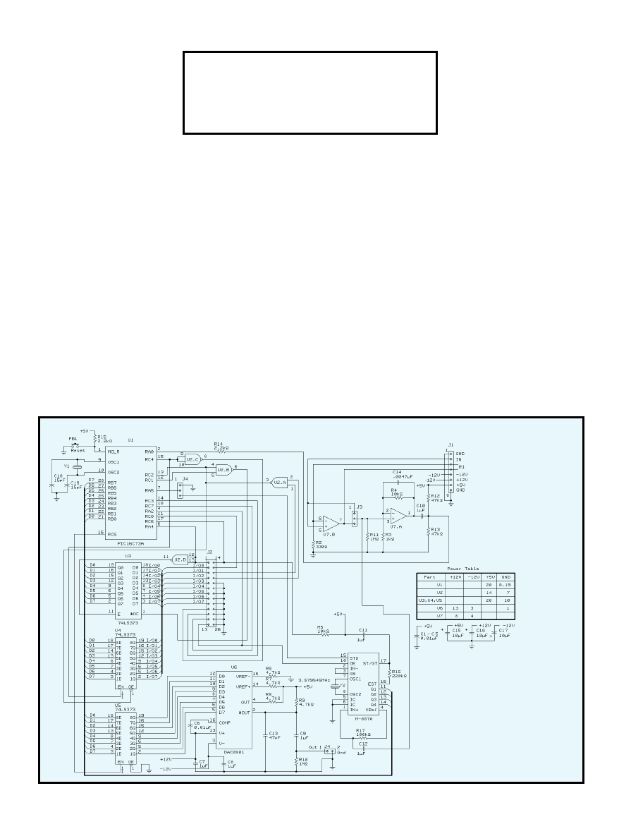
42
Issue 115 February 2000
CIRCUIT CELLAR
®
www.circuitcellar.com
U6 (a DAC0801) is driven
by the output of U5. The
audio output is taken from
pin 2. C11 and R9 filter out
the high-frequency compo-
nents, and C9 blocks DC.
Two gates of U2 are used
as inverters, one for the ACK
line and one for the STROBE
line. One gate holds PLAY low when
SELIN and INIT are both inactive
(high). The other gate enables the
PIC16C73 to tristate U3, except when
reading input from the PC (controlled
by RECV).
U8 receives the audio signal from
the line through C12. R17 feeds the
signal to the noninverting input (IN+).
GS is connected to the inverting input
(IN-) for 100 percent feedback, result-
ing in no amplification of the audio
signal. When SELECT is asserted, the
outputs of U8 are on the data bus (hi-
Z, otherwise).
THE POWER BOARD
Figure 3 shows the schematic for a
suitable power supply. It provides
+5 V, +12 V, and –12 V. The input
must be 12.6 VAC, which can be
connected to pins 5 and 6 of J5 or to a
power jack at J6. A heat sink is re-
quired for VR1.
The first step in construction is to
make the PC board. Registration is
critical during exposure. The cross
marks are provided for this purpose.
You will need a 7 × 10
²
, two-sided
photosensitized board, such as Kepro’s
S2-710G. Make two negatives, one for
each side. Punch small holes at the
registration marks with a sharp tack.
Using a wooden board as a base,
place a blank PC board on the base
and one of the negatives on top of the
board, emulsion side down, so the
pattern is within the borders of the
board. Mark one of the regis-
tration holes with a sharp
awl and drill it with a #60
bit. Use a plastic-headed tack
to hold the negative in place,
then mark and drill the other
registration hole. Remove
the tack and clean the debris
from the board and negative,
then re-pin the negative to the board
with two tacks.
Place a clean sheet of glass on the
negative with the edge against the
tacks (to hold the negative in contact
with the board). Expose the board
according to the directions for the
material used. Remove the glass and
negative, flip the board, and repeat the
process with the other negative. Be
sure the emulsion side is down.
Enlarge the registration holes to
5
¤
16
²
and drill
5
¤
16
²
holes at the other
two corners. Place
1
¤
4
²
6-32 machine
screws in the holes and secure them
with machine nuts to enable the de-
veloper and etchant to flow under the
board. Develop, etch, and tin the
board, then remove the screws and
Figure 2
—The PIC16C73 is
programmed to set T01F when
the Strobe line goes low.
O CCC B6
Pin 6 should be high, pins 13 and 17 should be low.
O CCC 1C
Pins 6, 13, and 17 should be high.
O CCC A4
Pins 6 and 17 should be high, pin 13 should be low.
O CCC AA
Pins 6 and 13 should be high, pin 17 should be low.
O CCC A6
Pin 6 should be high, pins 13 and 17 should be low.
O CCC AB
Pin 13 should be high, pins 6 and 17 should be low.
Table 2
—When you run DEBUG, substitute the port-control register address
(
DDD+2
) for
CCC
.

44
Issue 115 February 2000
CIRCUIT CELLAR
®
www.circuitcellar.com
cut the board along the outside rect-
angle. Use a #60 bit to drill holes
through all pads.
Solder in the vias (feed-through
conductors). Use 24 AWG bare
tinned copper wire. Place a piece of
conductive foam (like that commonly
used to ship ICs) under the solder
side. Press the wire through one of
the via holes completely through the
foam, and clip off the wire about
1
¤
4
²
above the board.
Place a number of vias in the board
(not all at the same time), then solder the
component side. Remove the foam and
place it on the component side, then
solder the solder side. Clip the wires
after both sides have been soldered.
Be careful not to solder a via or pad
intended for a component lead. Vias
always connect traces on both sides of
the board, but some pads are intended
for component leads. Because none of
the vias are under a component, the vias
can be soldered in after the components,
but that approach is more difficult.
Make good solder connections,
poor connections are difficult to trace.
Remove the rosin with acetone. Let
the acetone drip off the edge and then
check for good solder joints.
Solder in the components, from
smallest to largest. Again, be careful
to make good solder joints with no
bridges. Don’t solder ICs directly to
the board, use sockets.
Using the Sound Board
sound.exe, linked from the object modules compiled/
assembled from
sound.c, menu.c, and parcom.asm,
control the sound board.
dictate.bat executes
sound.exe. The command line is:
sound [filename] [noise]
where
[filename] is the name (with extension) of the
message file and
[noise] is a parameter that determines
the audio signal noise band. The filename defaults to
MMDDhhmm, where MM is the number of the current
month, DD is the day of the month, and hhmm is the hour
and minute of the current time. The filename must be
stated if the noise parameter is stated.
dictate.bat can be executed from the command line:
dictate <filename> [noise]
where
<filename> is required but cannot have an exten-
sion (default
.snd) and [noise] is optional. A file named
sound.cnf must be in the current directory. It must con-
tain two lines in ASCII format:
PPP
ZZ
where
PPP is the hex address of the parallel port and ZZ is
the noise parameter. A comment can follow the parameter
in each line if it is preceded by a space. A typical configu-
ration file might look like:
278 LPT2
16 noise band = 16/128
The noise parameter in the configuration file will be
ignored if the command line has the noise parameter
stated. This parameter is the range of the audio signal
level (in units of the ADC result) that will not be exceeded
by noise. Because this figure will never be absolutely zero,
it’s necessary to establish a range that will be exceeded
only when a user is talking or there is audio input from
other than a microphone.
The maximum sound level is 127, thus a parameter of
16 is
1
¤
8
the maximum level. When recording, each block of
16,384 bytes is stored in the
.snd file only if it contains at
least one byte with a value outside the noise band. A noise
parameter of zero will result in continuous recording, including
long silent intervals.
When
sound begins execution, the file is created if it
doesn’t exist, or opened for appending if it does exist. A menu is
displayed as:
Record Play Backup Forward reWind Erase Loop De-
lete Test Quit
Pressing the key corresponding to the uppercase letter in-
vokes the appropriate response:
• Record begins recording at the current block
• Play begins playing at the current block
• Backup backs up the file pointer one block
• Forward advances the file pointer one block
• reWind sets the pointer to the beginning of the file
• Erase sets the file size to zero and sets the pointer to the
beginning of the file
• Loop repeatedly plays the current block
• Delete writes data to the current block that plays back as
a 305-Hz tone
• Test invokes the test mode whereby the audio input is
heard from the speaker
• Quit terminates execution
Pressing any key while playing, recording, or looping will
halt the current function and display the menu, but will not
select a function even if it is a menu function key.
Select Test to set the recording level if using the micro-
phone input. Select Record to start recordingThe block counter
should begin to increment, indicating that recording is in
progress. While recording, long silences are effectively deleted
by not being recorded.
Pressing any key while recording will stop at the current
block. Recording will resume at the current block when record
is selected. The backup, forward, rewind, and erase functions
can be used to reposition the file pointer to any block.
To play the file, press W to rewind the file then select Play.
The current block number is displayed on the monitor, allow-
ing the file pointer to be positioned quite precisely to within
0.84 s by using the backup, forward, and rewind functions. A
single block can be played repeatedly by selecting Loop. The
current block can be bleeped by selecting Delete.
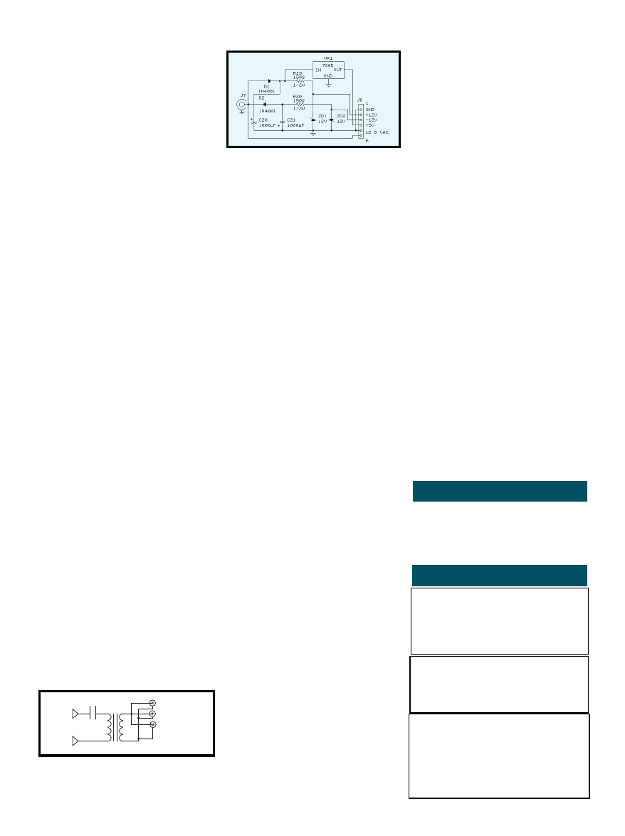
46
Issue 115 February 2000
CIRCUIT CELLAR
®
www.circuitcellar.com
THE PARALLEL PORT
Test the parallel port before con-
necting it to the sound board. Run
DEBUG as
D 40:8.
The display will show the base
address of up to three parallel ports
with the low-order byte first (7830 is
port address 378). Determine which is
the port that will be connected to the
sound board and proceed as follows,
where
DDD is the three-digit hex ad-
dress of the data register (base address)
and
CCC is DDD+2 (the address of the
control register):
O DDD 0 O CCC 0C I DDD
The display should show 00, indi-
cating the data register output is on
the pins:
O CCC AB I DDD Q
The display should show
FF, indi-
cating that the data register is
tristated. Also, the control register
pins will all be low. Leave the port in
this condition so all pins will be ei-
ther high impedance or near ground.
When the PC is powered up or
reset with the sound board connected
(powered or not), POST will probably
not recognize the port as a printer port
and will set the control register to
EBh so the data register is tristated
and all control lines are low. If it does
not recognize the port this way,
autoexec.bat should run INITPORT
DDD where DDD is the base address.
TESTING
Connect the power supply and
sound board. With no chips in the
sockets, check for correct voltages at
the Vdd/Vss pins and –12 V at pin 3 of
U6 and pin 4 of U7. Insert U2 in its
socket but do not connect any of the
other chips. Next, you should con-
nect the parallel port and apply power.
After you’ve applied power, run DE-
BUG as shown in Table 2.
Next, disconnect the parallel port.
Jumper pins 1 and 2 of J3, insert U7 in
its socket, and then apply power.
Apply a signal to the audio input jack
and test at pin 1. An audio signal gen-
erator and oscilloscope would probably
be useful but are not necessary.
The output signal can be measured
with a multimeter, set for an AC
range of 5 V or higher. Use a 0.1-µf
capacitor to block DC. Adjust R1 for
appropriate gain, depending on the
level of the input signal. The maxi-
mum output voltage with no clipping
is about 7-V RMS.
Program a PIC16C73 from
sound.
hex then insert the remaining chips
and connect a power amplifier with a
speaker to the audio output jack and a
microphone to the input jack. When
power is applied, the ADC and DAC
should be functioning and sound from
the microphone should be heard
through the speaker. Connect an au-
dio signal generator to the input and
select a level of about 100 mV. Adjust
R1 for the maximum gain that’s just
short of clipping. The output should
measure about 1.7 V RMS (5 V peak-
to-peak).
After you connect the parallel port,
run
SINE on the PC to create sine.
snd then run sound sine.snd and
select Play. You should get a 77-Hz
sine wave output. Run
sound test.
snd and select Test. Sound going into
the microphone should be heard from
the speaker. When you select Record,
the audio signal should be stored in
test.snd. After you are done record-
ing, rewind, select Play and the re-
cording should play back.
A TELEPHONE INTERFACE
A passive telephone interface is
shown in Figure 4. This simple inter-
Figure 4
—For the telephone interface, C1 blocks DC
and T1 tranfers the signal in both directions while
isolating the circuit from the line.
face is needed to run the telephone-
answering program,
telefone.exe.
See
telefone.doc for full instruc-
tions. Complete specs for a power
amplifier/telephone interface are avail-
able on the Circuit Cellar web site.
PROGRAMMING TIPS
Both the PIC16C73 and the PC
must be programmed efficiently in
order for them to operate fast enough
to achieve the high sampling rate and
exchange data rapidly. Interrupt-
driven processing is essential. The
source code for the programs I dis-
cussed earlier can serve as the basis
for further development of the sound
board. A 33-MHz 386 PC is the mini-
mum recommended.
I’d be glad to supply patterns for
the PC boards or transparent film, as
well as the software programs, but
please check the
REQUESTME.TXT file
that’s posted with the software for the
contact details.
I
Figure 3
—Here’s a look at the power supply I used for
this project.
T
el.
line
C1
.1
T1
1:1
Audio in
Audio out
Amplifier
250 V
Duane Perkins is a self-taught engi-
neer who has made computers and
electronics his avocation since retir-
ing in 1980. In recent years he has
specialized in PIC microcontrollers.
You may reach him at (717) 964-3536
or at dmperkins@compuserve.com.
SOFTWARE
The software, parts list, board tem-
plates, as well as additional appli-
cations are available for download
via the Circuit Cellar web site.
SOURCES
Kepro boards and film
Kepro Circuit Systems, Inc.
(800) 325-3878
(314) 426-2600
www.kepro.com
PIOC
B & B Electronics
(815) 433-5100
www.bb-elec.com
PIC16C73
Microchip Technology, Inc.
(888) 628-6247
(480) 786-7200
Fax: (480) 899-9210
www.microchip.com
48
Nouveau PC
edited by
Harv Weiner
50
Real-Time PC
A Matter of Time
Part 2: Using IRIG Codes
Ingo Cyliax
57
Applied PCs
A Personalized Virtual Web
Fred Eady
Photo courtesy of JK microsystems
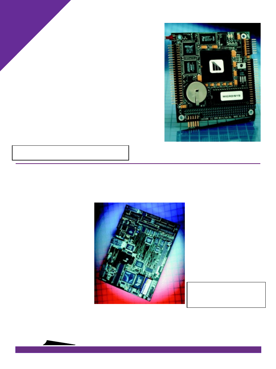
CIRCUIT CELLAR FEBRUARY
2000
48
NPC
www.circuitcellar.com
INDUSTRIAL SBC
The EPC-350 is an industrial computer that features the most
often needed I/O. It integrates serial, parallel, disk, analog,
digital, counter/timer, PC/104 expansion, and networking I/O
with a low cost-per-function. It is ideal for distributed control where
a number of computers are networked
through Ethernet. The variety of I/O
allows the EPC-350 to perform in a wide
range of applications.
The computer features a 386SX micro-
processor running at 40 MHz, supports
up to 16 MB of EDO DRAM, and includes
1 MB of flash memory. Support is also
provided for 512 KB of battery-backed
SRAM and a 144-MB DiskOnChip. I/O
consists of four 16C550-compatible se-
rial ports configured as RS-232/422/
485; a bi-directional ECP/EPP parallel
port; EIDE support for two hard disks;
SanDisk and CD-ROM drives; and 24-bit
programmable lines of digital I/O. The
unit also features eight channels, single-
ended (four differential) analog input,
two analog output channels, two 16-bit
PC
Nouveau
edited by Harv Weiner
PC/104 FORMAT 486 COMPUTER
The SBC1486 is a PC/104 form factor computer based
on the 486DX 32-bit microprocessor core that features up to
64 MB of RAM, 72 MB of flash memory, AT-compatibility, and a
SuperVGA output. SBC1486 systems can run large applications
without any mechanical disk drives, offering high reliability real and
protected mode operation. The computer can boot DOS, Windows 95/98/
NT, Linux, Windows CE, and other PC-compatible operating systems.
The SBC1486 core includes the 486DX processor at speeds from 66 MHz to
133 MHz, onboard cache, 64-bit DRAM, hardware floating point, and AT-
compatible interrupt, timer, and DMA. Onboard I/O includes COM1, COM2,
LPT1, SuperVGA, and a touchscreen or matrix keypad interface. The SuperVGA
is capable of driving CRT monitors and flat panel displays, with resolutions to
1024 × 1024. I/O expansion can be added onto the PC/104 connector, which
accepts 8-bit and 16-bit PC/104 cards. A free development kit is available that
includes cables, sample software, and full documentation.
The 72-MB flash memory space provided on the SBC1486 provides solid-state
storage for large applications. Micro/sys installs a ready-to-run firmware system on
the SBC1486 at no cost. This firmware includes a complete industrial BIOS, and
creates a DOS-like execution environment immediately upon power-up.
The basic SBC1486 is $495 in single quantity.
Micro/sys, Inc. • www.embeddedsys.com
(818) 244-4600 • Fax: (818) 244-4246
counters, real-time clock, support for two floppy drives, keyboard
connector, and PC/104 expansion connector.
The EPC-350 is designed for a temperature range from –40° to
85°C and can withstand high shock and vibration. The card has a
remotely read ambient temperature sen-
sor that is accurate to ±3°C over the full
temperature range. The low power con-
sumption allows the card to be placed in
sealed enclosures without the use of a
fan. The simple operator interface of a
keypad and 4-line LCD display is fully
supported with driver software. The EPC-
350 is 5.75
²
× 8
²
(EBX outline).
The card comes with DOS 6.22
installed in flash memory, and supports
QNX and Linux. The single quantity
price is $595.
Octagon Systems
(303) 430-15O0
Fax: 303-412-2050
www.octagonsystems.com
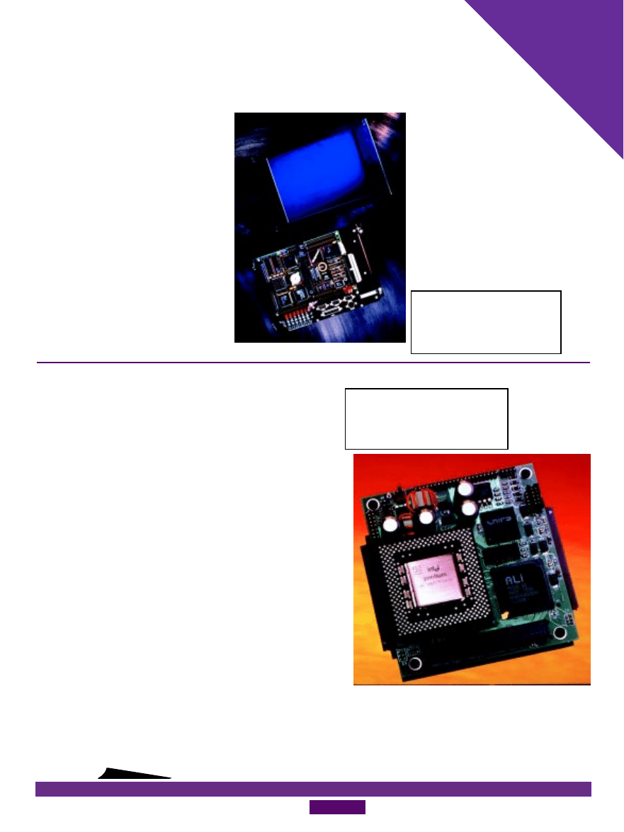
FEBRUARY
2000
E
MBEDDED
PC
49
NPC
www.circuitcellar.com
PC
Nouveau
The TFT panel provides high luminance
(250 cd/m
2
) and 640 × 480 pixel resolution with
262,144 colors. A wide viewing angle of 50° up, left
and right, plus 35° down permits
easy placement and maximum op-
erator viewing flexibility. The contrast
ratio is 300:1.
The back of the Panel PC is designed for
easy access and connection to I/O and
power cables. Simple terminal strips are
provided for the power source. A separate
panel terminates the LPT, keyboard, and
COM channels for easy hook up to industry
standard cables.
A Panel PC that includes the 133-MHz
LBC-586Plus and 10.4
²
AM color TFT
panel lists for $2795.
WinSystems
(817) 274-7553
Fax: (817) 548-1358
www.winsystems.com
FLAT PANEL DISPLAY PC
WinSystems’ Panel PC is a compact, full-featured PC that
includes a 640 × 480 flat panel VGA display, 133-MHz Pentium-
class PC with Ethernet and PC/104 expansion, plus optional
touchscreen. The Panel PC is built upon a black
anodized aluminum frame that holds the 10.4
²
Active Matrix TFT LCD panel, backlight in-
verter, touchscreen and controller, single board
computer, plus the video adapter card and
cables. It is designed as an open frame unit for
mounting inside a customer’s enclosure. Appli-
cations include test instrumentation, medical
devices, machine control, and kiosks.
The computer consists of the WinSystems’
LBC-586Plus-133 SBC. It is a 133-MHz 5x86
with 256 KB of cache, video, four serial ports,
LPT port, 10 Mbps Ethernet, IDE and FDC
controllers, 48 digital I/O lines, and solid
state disk support up to 144 MB using
DiskOnChip. The LBC-586Plus is a fully x86-
compatible embedded PC. It supports stan-
dard operating systems, real-time executives,
utilities, and standard drivers.
PC/104-PLUS SBC
The Panther is a performance-oriented processor board in a compact
PC/104-Plus format. It is a complete single-board computer that can be
used alone or with expansion modules. It is fully compatible with Windows
NT/95/98, Windows CE, Windows NT Embedded, QNX, Linux, RT-
Linux, OS-9, and other RTOSs.
The processor module supports standard socket 7 (MMX/3D class)
CPUs up to 400 MHz, including Pentium, K6, K6-2, K6-III, and the low-
power K6-2E for fanless operation. This is made possible by its unique two-
board design with PC/104-plus interconnect. The Panther is designed to
mount at the top of a PC/104 stack due to fan/heat sink height.
The Panther accepts up to 128 MB of low-power system RAM and up
to 72 MB of bootable DiskOnChip flash memory. It includes 512 KB of
Level II cache. A pair of high-density I/O connectors supports standard I/O
including floppy and IDE interface, CRT/flat panel interface, two COM
ports (one configurable as RS-232/422/485), LPT, and dual USB ports.
The 10/100 autodetect Ethernet interface is ideal for systems that are
running at 10 Mbps now but may be upgraded to 100 Mbps in the future.
Additional features include a watchdog timer, Ethernet remote boot
option, single voltage (+5 V) operation, voltage sensing reset circuit, and
reprogrammable BIOS.
Panther versions include AMD K6-2 3D Now CPUs in 266 or 400 MHz.
Both are priced under $1000 in low OEM quantities. A fanless low-power
266-MHz version will be available in about the same price range.
VersaLogic Corp.
(541) 485-8575
Fax: (541) 485-5712
www.VersaLogic.com

RPC
CIRCUIT CELLAR FEBRUARY
2000
50
www.circuitcellar.com
Table 1—IRIG formats vary by the pulse/bit rate. Faster codes
are used for higher resolution.
R
eal-
T
ime
PC
I
ngo Cyliax
A
Matter of Time
Part 2: Using IRIG Codes
L
Ingo sets out to explain the ins and outs of working with one of the most
popular time codes—IRIG. Once you understand the details, you'll have your
PC clock synchronized with an existing time standard in no time.
ast month, I introduced you to time
issues. We learned that most PC clocks
are not accurate and that you need at
least a temperature compensated or even
a Cesium or Rubidium time standard to
achieve any sort of high-accuracy clock.
If you don’t have the budget for that, you
can approximate the accuracy and stabil-
ity by synchronizing your PC to an exist-
ing time standard, like a radio clock
signal or perhaps the global positioning
system (GPS).
Finally, we learned that most time
standards use a time code to transmit time
information. I want to show you one
of the time code standards in detail
and look at a sample application
that generates a time code signal
with a PC and how to synchronize
the PC to an external time standard.
Of all the time codes, IRIG is the
most popular. It was developed in
the ’50s to synchronize various test
and tracking instruments for missile
testing. There are actually several variet-
ies of IRIG time codes. They differ in the
format, precision, and encoding. IRIG
codes can be transmitted via coax, twisted-
pair cables, RF, and then recorded on
analog tape recorders. It’s also easy to
decode in hardware, if necessary.
IRIG codes are transmitted serially by
encoding bits into a pulse-width coded
symbols. The bit rate of the code is de-
fined by the format of IRIG code used as
summarized in Table 1.
There are three types of symbols—
Zero, One, and a position identifier. A
Zero is defined as a pulse that has 20% of
the bit time. So, an IRIG-A code for zero
that has a 1000-pulse per second (pps)
rate or a bit time of 1/1000 (i.e., 1 ms),
is 0.2 ms long. A One is 50% and a
position identifier is 80%, or 0.5 ms and
0.8 ms respetively, in a IRIG-A code.
Each frame is divided into 10-bit words.
The last bit of each word is a position
marker, which leaves nine bits of payload
data. There are 10 such words in each
frame, except for IRIG-D and IRIG-H for-
mats, which have six words. At the start of
the frame, there is also a reference marker.
This reference marker is just like a
position identifier. So, if you see a
sequence of two 80% pulses, you
know that the second pulse just
started the frame.
The data transmitted in IRIG code
conveys the time and other data,
such as configuration information.
Time data in each frame identifies
the time at the start of that frame.
Format
Bit rate
Bits per frame
Frame rate
A
1000 pps
100
10 fps
B
100 pps
100
1 fps
D
1 ppm
60
1 fph
E
10 pps
100
6 fpm
G
10 pps
100
100 fps
H
1 pps
60
1 fpm

FEBRUARY
2000
E
MBEDDED
PC
RPC
51
www.circuitcellar.com
The current time since the beginning of
the year is encoded in BCD. The resolu-
tion of the data depends on the code
format, because the frame rate is different
for each format. For example, in IRIG-H
format the frame period is 1 min., so the
data within the frame only counts the
minutes.
Optionally, the SBS (straight binary
seconds) count indicates the seconds that
have elapsed at the beginning of the
frame since the beginning of the day. This
data is encoded as a binary number and
not BCD. The optional configuration data
can be used to transmit other data be-
tween instruments and is vendor specific.
Table 2 shows the word encoding for
the IRIG-B code I’ll be using. As I showed
you in Table 1, IRIG-B has 100 bits in a
frame, which lasts one second. This means
that each bit is trans-
mitted at a 100-pps rate.
A Zero is 2 ms, a One is 5 ms,
and a position identifier is 8 ms
long. The time being referenced is
at the rising edge of each pulse. In
IRIG-B, the rising edge of the first bit in the
frame thus identifies the exact second,
and the rising edge of each pulse identi-
fies the hundredths of a second.
IRIG codes can be transmitted in three
different modulation schemes. One is DC-
level pulse-width encoding, where we just
transmit the IRIG signal as digital pulses.
Each bit is a digital pulse with specific
width depending on the bit value being
transmitted. Transmitting IRIG in this way
works best when we want to transmit it
over short distances.
Another way to send IRIG codes is by
amplitude modulating a carrier frequency.
The carrier frequency is derived from the
master oscillator of the time code genera-
tor and thus locked to the actual time code
being transmitted. This means that a zero
transition of the carrier indicates the start
and stop of the pulse being transmitted.
The length of the pulse is a whole number
of carrier waves.
By using a synchronous carrier like
this, you can extract a higher resolution
time signal than actually transmitted by
the pulses in the time code. The accuracy
is limited to how well you can lock onto the
carrier and determine the zero-crossing
points. Because the carrier frequency is
typically 10× higher then the bit rate, an
AM-modulated IRIG signal will take more
bandwidth to transmit a record.
Finally, IRIG codes can be transmitted
via Manchester digital codes. Manches-
ter offers a compromise between DC-level
pulse codes and AM-modulated carrier.
Using the Manchester codes requires twice
the bandwidth of a pulse-width code, but
allows better resolution and a way to
recover a clock signal from the datastream.
Like the AM modulation scheme, Manches-
ter codes have a zero DC bias and are not
polarity sensitive.
Figure 1 shows how a sample word is
encoded in the three different modulation
schemes. To make it easy to identify which
IRIG code a piece of equipment can
generate or decode, there is an identifica-
tion scheme for IRIG codes. I’ve already
shown you that we use letters to identify
the speed/precision of the code. In addi-
Listing 1—The initialization function (needed by a RT-Linux real-time module) lets you
initialize the task control block and a timer.
RT_TASK bitwrtask;
/* task control block*/
int init_module(void)
{
printk("Starting IRIG Module\n");
/*disable interrupts on the parallel port*/
outb(0x00,LPT_PORT+2);
/*setup a task*/
rt_task_init(&bitwrtask, irig_wr, 1, 3000, 4);
/*arrange it to run the task at a rate of 1000 Hz*/
rt_task_make_periodic(&bitwrtask, rt_get_time(), PERIOD);
/*everything OK*/
return 0;
}
Listing 2—Here’s a look at the main code for generating an IRIG-B on the parallel port.
unsigned int ticks;
int ten,sec,min,hrs,day;
void irig_wr(int t) {
register int bit,cycle;
register unsigned char out;
register val = 0;
ticks = 0;
out = 0;
val = ZERO;
while (1) {
outb(out,LPT_PORT);
bit = ticks/10;
cycle = ticks % 10;
switch(bit){
case 0:
/*reference bit*/
val = REF; break;
case 9:
/*position markers*/
case 19:
case 29:
case 39:
case 49:
case 59:
case 69:
case 79:
case 89:
case 99:
val = MARK; break;
case 1: val = (sec & 0x1); break;
case 2: val = (sec & 0x2)>>1;
break;
case 3: val = (sec & 0x4)>>2;
break;
case 4: val = (sec & 0x8)>>3;
break;
(continued)

CIRCUIT CELLAR FEBRUARY
2000
52
www.circuitcellar.com
Listing 2—continued
case 6: val = (sec & 0x10)>>4; break;
case 7: val = (sec & 0x20)>>5; break;
case 8: val = (sec & 0x40)>>6; break;
case 10: val = (min & 0x1);
break;
case 11: val = (min & 0x2)>>1; break;
case 12: val = (min & 0x4)>>2; break;
case 13: val = (min & 0x8)>>3; break;
case 15: val = (min & 0x10)>>4; break;
case 16: val = (min & 0x20)>>5; break;
case 17: val = (min & 0x40)>>6; break;
case 20: val = (hrs & 0x1);
break;
case 21: val = (hrs & 0x2)>>1; break;
case 22: val = (hrs & 0x4)>>2; break;
case 23: val = (hrs & 0x8)>>3; break;
case 25: val = (hrs & 0x10)>>4; break;
case 26: val = (hrs & 0x20)>>5; break;
case 30: val = (day & 0x1);
break;
case 31: val = (day & 0x2)>>1; break;
case 32: val = (day & 0x4)>>2; break;
case 33: val = (day & 0x8)>>3; break;
case 35: val = (day & 0x10)>>4; break;
case 36: val = (day & 0x20)>>5; break;
case 37: val = (day & 0x40)>>6; break;
case 38: val = (day & 0x80)>>7; break;
case 40: val = (day & 0x100)>>8; break;
case 41: val = (day & 0x200)>>9; break;
case 45: val = (ten & 0x01);
break;
case 46: val = (ten & 0x02)>>1; break;
case 47: val = (ten & 0x04)>>2; break;
case 48: val = (ten & 0x08)>>3; break;
default: val = ZERO; break;
}
/* -- on -- */
if (cycle == 0){
if(val == REF)
out = 0x03;
else
out = 0x01;
}
/* -- zero -- */
if (cycle == 2 && val == ZERO){
out = 0x00;
}
/* -- one -- */
if (cycle == 5 && val == ONE){
out = 0x00;
}
/* -- mark -- */
if (cycle == 8){
out = 0x00;
}
/*
wait for next tick
*/
ticks = (ticks + 1)%1000;
rt_task_wait();
}
}
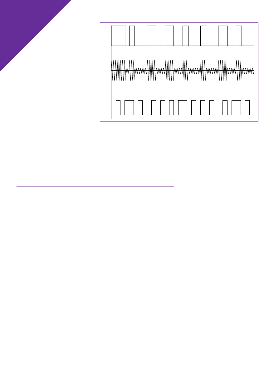
RPC
CIRCUIT CELLAR FEBRUARY
2000
54
www.circuitcellar.com
Mark
0
1
1
1
0
0
0
Figure 1a—IRIG code without modulation is essentially pulse-width modulation represented as
DC levels with a modulation ratio of 10:3. b—In AM-modulated IRIG, the pulse modulates the
amplitude of the carrier, which is 10× the bit rate. The ratio of on/off can range from 3:1 to 6:1.
c—With Manchester-coded IRIG, the pulse code is XORd with a clock signal that is twice the bit
rate. To decode, you XOR the received signal with a recovered clock signal.
a)
b)
c)
tion, there is a three-
digit identifier that in-
dicates the type of data
the code includes, the modu-
lation type, and the frequency/
resolution used.
SOFTWARE TO KEEP TIME
Got all that? Let’s look at some soft-
ware for generating an IRIG-B000 code.
Remember, this is a 100-pps format code
that is transmitted as a DC-level pulse
train, and I’ll send the current time as BCD
encoded data.
A couple of months ago, I discussed
using the PC parallel port hardware to do
a few things. This month, I’m using the
parallel port to generate an IRIG code. I
like using the parallel port on PCs. It’s
always there and most of my projects
don’t use a printer anyway.
Let’s recap. The parallel port on a PC
has three registers. The data register lets
you send eight bits of data out of the
computer. There are also four control pins
in the control register that can be used as
output (and input), and five input pins that
are normally used as status signals from
the printer. The port has one pin that can
be configured to generate an interrupt.
To program the parallel port, I just
have to use inp/outp instructions. There’s
nothing I have to do to initialize the
parallel port hardware, unless I want to
use the interrupt request feature.
I will send the IRIG code on the d0 line
of the parallel port. Also, on d1, I’ll send
a pulse-per-second output, which signals
the beginning of a new frame. This pps
signal is not part of the IRIG spec, but it’s
nice to have—especially during debug-
ging, when you can use it to trigger an
oscilloscope or logic analyzer.
For this project, I’m going to use RT-
Linux, although any RTOS-like operating
system will work if the interrupt latency for
the timer service is acceptable for your
application. I’ve written about RT-Linux in
the past. It’s a real-time extender for the
Linux OS. The real-time processes (or
threads) are loaded as modules into the
Linux kernel address space. Once they
are there, they have access to all of the
hardware resources and physical memory.
There is also a library of services that
can be loaded with the RT-Linux applica-
tion modules. These services provide an
API for thread management, timer ser-
vice, communication services, and inter-
rupt vector management.
The RT-Linux extender manages all of
the real-time threads, timer hardware,
and interrupts. When there are no real-
time threads to run, the scheduler invokes
the Linux operating system as the lowest
priority thread. Real-time threads can
communicate with Linux processes using
FIFOs or shared memory. These FIFOs are

FEBRUARY
2000
E
MBEDDED
PC
55
www.circuitcellar.com
Figure 2—With format/modulation identifier
systems for IRIG codes, in theory, equipment
with matching designators can communicate.
Coded Expressions
0 - BCD, CF, SBS
1 - BCD, CF,
2 - BCD,
3 - BCD, SBS
Frequency/Resolution
0 - No Carrier
1 - 100 Hz/10 ms
2 - 1 KHz/1 ms
3 - 10 KHz/0.1 ms
4 - 100 KHz/10 s
5 - 1 MHz/1 s
Mod. Frequency
0 - None use pulse width
1 - sine wave, amplitude mod.
2 - manchester encoding
Format
A - 1 K pps
B - 100 pps
D - 1 ppm
E - 10 pps
G - 10K pps
H - 1 pps
special device entries under Linux and are
an API under RT-Linux.
Shared memory is a little more compli-
cated to use. Basically, you reserve some
physical memory that the Linux kernel
doesn’t know about. RT-Linux threads have
access to this memory region, and Linux
processes can also map the memory into
their virtual address space. You must use
your own locking protocol to protect criti-
cal regions when using shared memory.
I’ll only use the interrupt vector and
timer services out of RT-Linux for this project.
For the IRIG-B format, I must generate
pulses at a 100-Hz rate. The pulses need
to have pulse lengths of 2 ms, 5 ms, and
8 ms. To get these pulse lengths, I need a
timing resolution of 1 ms, which is easily
done with a 1000-Hz timer interrupt.
To start the ball rolling under RT-Linux,
I have to provide an initialization routine.
The routine in Listing 1 creates a real-time
thread by allocating a stack of 3000
bytes to it. I also specify to pass an
argument of “1” to it, although it’s not
used. Finally, I assign a priority of 4 to the
task. This priority is arbitrary because it’s
the only task running, for now.
The task-control block (bitwrtask) is
allocated globally in our example, al-
though it doesn’t have to be that way.
Finally, I set off the timer to schedule my
IRIG task once every 1 ms (1000 Hz). A
return code of 0 means that everything is
OK and to keep my module resident.
At this point, my task wakes up once
every millisecond. The first time it wakes
up, the task intializes variables. One

RPC
CIRCUIT CELLAR FEBRUARY
2000
56
www.circuitcellar.com
Word position
Description
0
BCD time of year (seconds)
1
BCD time of year (minutes)
2
BCD time of year (hours)
3
BCD time of year (days)
4
BCD time of year (days)
5
CF control functions
6
CF control functions
7
CF control functions
8
SBS time of day (seconds)
9
SBS time of day (seconds)
Table 2—These are the word assignments for an IRIG-
B–format time code.
REFERENCES
Range Commanders Council, “IRIG Serial Time Code
Formats”, IRIG Standard 200-98, http://
tecnet0.jcte.jcs.mil:9000/RCC/oldoc.htm
Datum, Inc., “Timing & Time Code Reference”,
www.datum.com/res_technical.html
Ingo Cyliax has written for Circuit Cellar
on topics such as embedded systems,
FPGA design, and robotics. He is a re-
search engineer at Derivation Systems Inc.,
a San Diego–based formal synthesis com-
pany, where he works on formal-method
design tools for high-assurance systems and
develops embedded-system products.
You
may reach him at cyliax@derivation.com.
variable is the tick
counter, which is
incremented once every
time the task is awakened.
You can use the tick counter to
compute the current bit position
you’re on. There are ten ticks for each
bit period. Finally, there is a variable that
represents the state of the current symbol
and another variable that represents the
current output state of the signal. After
that, the task stays in the big
while() loop.
Each time through the loop, I set the
output pin of the parallel port to the state
that was computed in the previous loop
execution. This might seem odd at first, but
to reduce the jitter in the IRIG signal, I
want to reduce the uncertainty in the
interrupt latency when the timer goes off.
If I set the value right after I wake up, I
reduce the uncertainty that the code intro-
duces when computing the value. This
computation is now done at the end of the
process, where it won’t affect the latency.
Each bit time has a case entry associ-
ated with it. There are four general classes
of cases—the position identifiers, the mark
position, the bit positions with varying
data, and all of the bits that are
always zero. You use the macros
MAR, REF, ZERO, and ONE to
assign a symbol value. Once you
set the symbol value for the current
bit, you drop to the pulse-width
timing section.
This section is executed on each
clock tick. I compute a cycle that is
the relative tick position inside a bit
period. The cycle can go from 0
(the beginning) to 9 (the end).
At cycle zero, the output value
gets set to a logic one level be-
cause you always have a rising edge at
the beginning of each pulse. Depending
on the symbol value, you reset the pulse.
This would be at cycle two for a ZERO,
cycle five for a ONE, and cycle eight for
either a MARK or REF. The output state for
the next tick is now set and you make a
call to
rt_task_wait(), which will suspend
this task until it is awakend again by the
timer. Then it all starts over again.
Once again, I’ve run out of time. Next
month, I’ll to show you how to hook up an
external timing reference and how to
synchronize an IRIG stream to it.
RPC.EPC
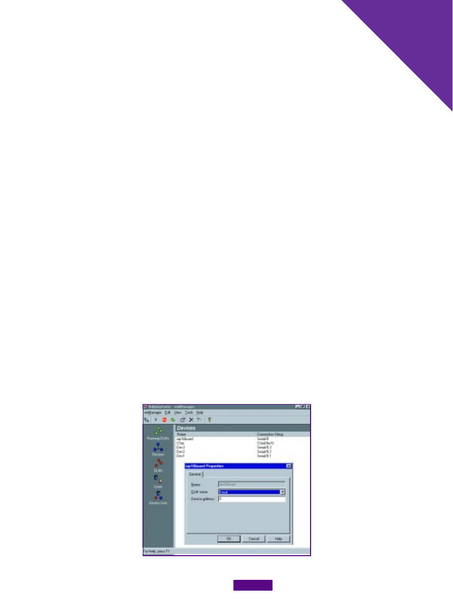
FEBRUARY
2000
E
MBEDDED
PC
APC
57
www.circuitcellar.com
A
pplied
PC
s
F
red Eady
Putting source code and CAD copy on the ‘Net is a good thing for all, but what
if you wanted to pass “physical” information between a couple of pieces of
hardware? Fred uses EMIT and a PIC to show us just how easy that can be.
H
ave you noticed that everything seems
to be going to the Internet in one way or
another? Even this time-honored publica-
tion has an Internet cohort. (And a good
one at that. If you haven’t already visited
Circuit Cellar Online, you should.)
Don’t get me wrong. The Internet is
thriving and I think that’s great. As you
can probably deduce from my e-mail
address, I have my own domain on
this aged-but-very-popular medium, too
(mainly to “give away” code, sche-
matics, PC board layouts, and ideas
from past and present).
Being able to put source code and
CAD copy on the ’Net is a good thing
for all of us, but what if you want to use
the Internet as a conduit to pass physi-
cal information between a few pieces
of hardware? Not just any old John or
Jane hardware, but hardware you
designed and built.
If you don’t have the funding for the
interface equipment or the right con-
tacts, you can’t do that on the real
Internet. OK, let’s assume you’re Internet
poor and don’t know the right people to
fund your lift on the web. That means you
can’t gather that temperature or humidity
data from your wine cellar (or anybody
else’s) over the ’Net.
Don’t fret, you can use the same
“Internet” tools to get your data’s worth
via dial-up, an Ethernet LAN, or direct
serial connection. Best of all, the Internet
tools that help you do this are free (via the
Internet, of course).
LED AT THE END OF THE
TUNNEL
A problem I often have when do-
ing these articles is guessing what you
will want to do with the information I
present. Some of you will want to
measure the angle of deflection of a
particle beam bounced off a piece of
Kryptonite. Others will want to know
how much water is in the basement
after a hard rain. And, some of you
will want to turn on the coffeepot while
checking the morning’s e-mail. Well,
in this how-to segment, I will supply the
basics for doing all of the above.
I’ll use two levels of embedded
technology (an embedded sandwich
if you will) to show you how to move
A
Personalized Virtual Web
Photo 1—The name is what you want it to be but the DLM must
match your physical connection.
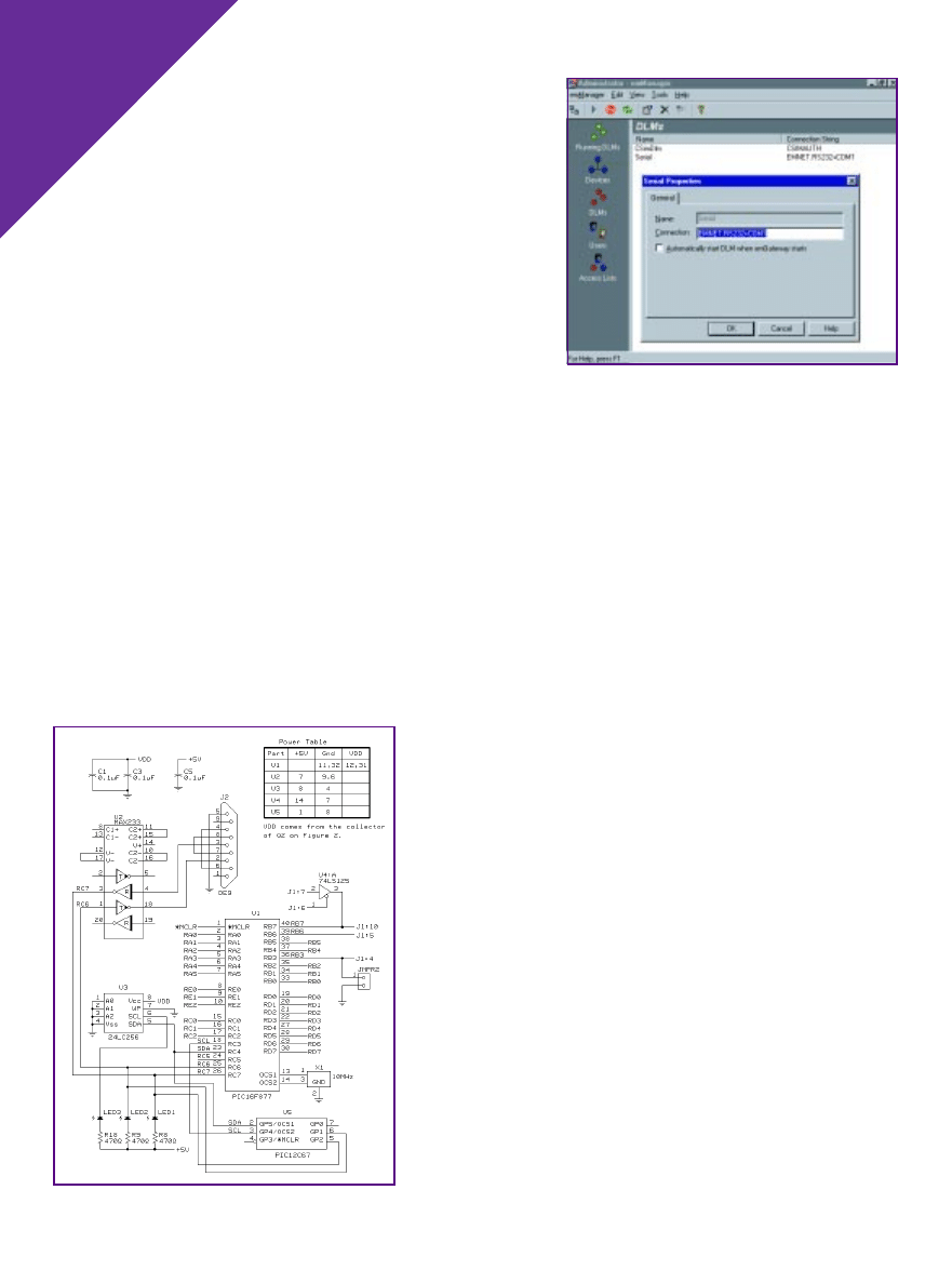
APC
CIRCUIT CELLAR FEBRUARY
2000
58
www.circuitcellar.com
WHY THIS AND THAT
Because this is an embedded
PC forum, you’re probably won-
dering if I made some sort of
deal with Bill in that I’m using
Win9X. The reality is that
emWare’s development pack-
age is designed to be universal
as well as easy to install and
bring up. Most of us have a copy
of Windows and the free
downloadable emWare modules
run on Win95/98 and NT with
service pack 3. If you have spe-
cial OS needs, contact the
emWare technical support folks.
You may also be wondering
why PIC. Well, because I have
all of the tricky stuff for PICs. The concepts
here also apply to Hitachi, Philips, Intel, or
any other micro you can stuff bits into. If
PIC is not your thing, download the EMIT
code package for your processor of choice.
Another reason for choosing the
PIC16F876 is that you can program it on-
the-fly in-circuit without +13 VDC pro-
gramming circuitry. The “F” in PIC16F876
stands for flash memory and this part is a
grown-up PIC16F84 with 8k words of
program flash memory, 368 bytes of user
RAM, and 256 bytes of user EEPROM.
More importantly, the PIC16F876 in-
cludes a 5-channel 10-bit ADC
and at least 10 available digi-
tal I/O lines. An internal USART
provides our portal to the vir-
tual internet and internal I
2
C
communication hardware al-
lows the addition of external
serial EEPROM or other I
2
C
slave devices if they are
needed.
Not only do you know
“why,” but you’ve probably
figured out “what,” as well.
Our virtual internet is really a
direct-connected and properly
terminated CAT 5 cable, a
dial-up phone connection, or a
private Ethernet LAN physically
connected to an embedded PC.
The embedded PC, our vir-
tual router, ties directly to the
PIC server via a standard se-
rial connection. At the server
end of our virtual Internet will
be the PIC16F876 device filled
with EMIT supervisor code and
some user-written PIC code to gather “pol-
len” from sensors and switches. This sen-
sor data is processed by the EMIT/user-
written code combination and placed on
the virtual ’net using an embedded PC as
a virtual router.
Just like on the real Internet, John and
Jane Doe access the EMIT-enabled
PIC16F876 server by jumping on the
virtual ’net and contacting the virtual router.
A URL that points to the EMIT-enabled PIC
server is entered and data is transferred to
and from the server device. Unlike the
dedicated servers you find on your tradi-
tional Internet, the PIC server can also be
instructed to drive its digital I/O from the
web browser interface and the status of
the digital I/O pins can be sensed at the
web-browser level.
VIRTUAL WEB COMPONENTS
As you’ve already seen, on the out-
side, our little virtual ’net is much like the
real one. The routers, servers, and hosts
are identical, they’re just using addresses
relevant to a private internet rather than a
public Internet. Each web component has
a purpose that’s defined by its internal
operating code. Let’s start by taking a look
at what makes up the PIC16F876 server.
The operation of the PIC16F876 is
dictated by the EMIT algorithms it ex-
ecutes. This code is formally known as
emMicro. It works in tandem with user-
written code to process data derived from
functions, events, and user-defined variables.
To make data transfers more efficient,
emMicro uses Microtags to abbreviate the
data passed from its internal registers to
the virtual router or gateway device. Us-
Internet-less informa-
tion from the switch and
sensor to a web browser.
Put simply, I’m going to as-
semble a virtual internet using
LAN cabling that you can buy or
assemble in your living room.
The first level of embeddedness con-
sists of any embedded PC capable of
running Win95 or Win98 in a minimal
configuration. The second embedded level
belongs to Microchip in the guise of the
PIC16F876.
A basic edible sandwich consists of
two pieces of bread with some middle
ingredients, like a meat product and some
veggies. The meat and veggies of our
embedded sandwich is EMIT—emWare’s
any-device, any-network application.
EMIT version 3.0.3 is on the streets and
there seems to be a new sheriff in town.
The PIC support is greatly enhanced and
the documentation is more thorough. Ver-
sion 3.0.3 doesn’t come with “paperware”
because the entire documentation is
downloadable as an Adobe PDF docu-
ment. All you have to do is go to the
emWare web site and download all of the
info and software to EMIT-enable a
PIC16C73. Then continue with the next
section to learn how to apply your newly
acquired tools to a PIC16F876.
Figure 1—Simple, elegant, effective.
Photo 2—The idea here is that, in standard serial mode,
you can have as many devices as you have physical
serial ports.
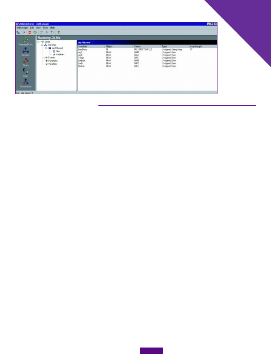
FEBRUARY
2000
E
MBEDDED
PC
APC
59
www.circuitcellar.com
ing the Microtag approach also allows
the PIC server to serve up documents as
well. These documents are standard HTML
content and can be stored in the PIC server
itself using the EEPROM I mentioned ear-
lier or in the gateway device. Data is
transferred from the PIC server to the
gateway device using emNet, which re-
sides on both the server and the gateway.
Each device or server may communi-
cate with the gateway as a serial device,
a multidrop device, or LAN device, and
must be configured accordingly. In our
virtual internet environment, the server
communicates with the gateway serially.
This is defined using emManager.
As you see in Photo 1, I’ve named our
server “iap16board” and assigned a con-
nection string of “Serial/0”. This desig-
nates a single serial connection between
the server and gateway devices.
If I wanted to add other iapboards in
this fashion, I would have to define each
separately and have a serial port on the
gateway for each connected server de-
vice. For multiple servers, RS-485 multidrop
is a better way to go. The “DEVx” devices
you see in Photo 1 designate multidrop
devices addressed as 1, 2, and 3. For the
time being, I’m going to stick with the
single serial connection.
Notice also in Photo 1 that the DLM
name for the iap16board is “Serial”. DLM
is the acronym for device link module.
Each device must have a corresponding
DLM. The DLM helps finish the connection
definition I started and defined in the
device-definition portion of emManager.
Photo 2 shows that the Serial DLM ties
the emNet connection to our PIC server as
an RS-232 serial connection on COM1 of
the gateway device. For a server device
to communicate using emNet, its corre-
Photo 3—If you want
to see it or manipu-
late it, it must be
listed here.
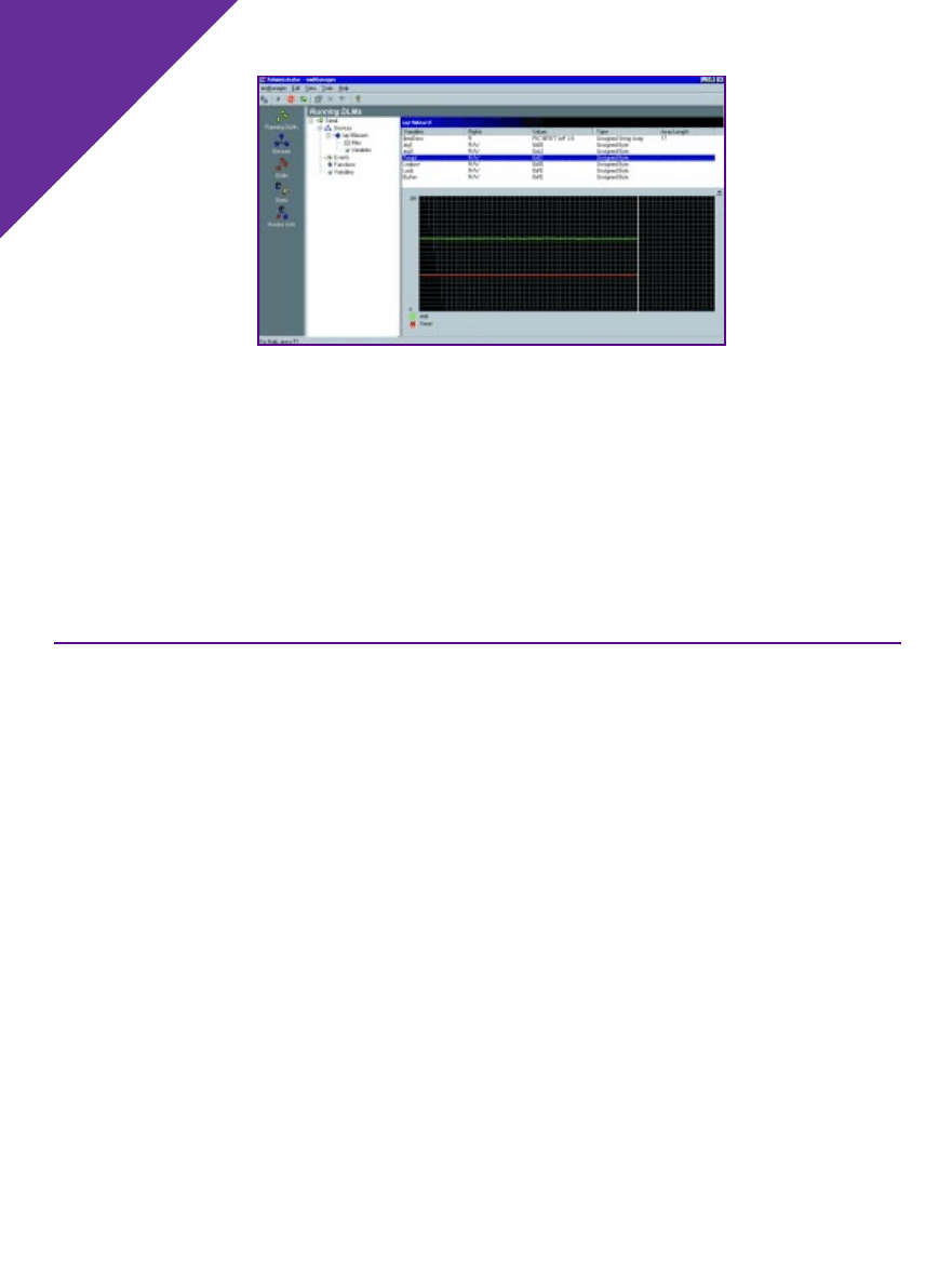
APC
CIRCUIT CELLAR FEBRUARY
2000
60
www.circuitcellar.com
sponding DLM must be loaded and run-
ning on the gateway device.
Photo 3 is a screenshot of our Serial
DLM running and connected via emNet to
our PIC16F876 server. Note the range of
variables in the variables column. These
are actual variables in the PIC server code
that I have defined and used to collect
temperature data.
The purpose of these variables here is
twofold. First, they are required here if
they interact with the web browser’s Java
interface. Second, if I want to monitor their
values while the PIC server is serving, I
can subscribe to them. Subscribing to a
variable enables me to see its value
change dynamically as the PIC server
code executes.
The screenshot in Photo 4 shows the
relationship between the final tempera-
ture value,
Tempf, and the original raw
captured value,
arg0. Not too shabby for
a country boy, huh? Note the hierarchy in
this screenshot. Our Serial DLM is running
and is talking to our device, the
iap16board, which contains variables
arg0, arg1, Tempf,
Ledport, Leds, and
Button.
The data transferred
by emNet and interfaced
by the DLM is sent to the
device access service for
transportation across the
virtual ’net. In addition,
the gateway (which is
running emGateway and
emManager) is also an
HTTP server. While the
device access service
interfaces with the web
browser’s Java interface, the HTTP server
serves up emObjects, which are used by
JavaScript to make pretty pictures on the
client’s browser.
Other things are going on here, too.
Remember the Microtags? Well, if they
are transferred to the browser machine,
they are expanded at the gateway level.
That’s how it works on the conceptual
level. We still have to build a GUI inter-
face and write some PIC code. I still have
to show you how to program that ’876,
too. As Garth would say, “Let’s git after it!”
Photo 4—
The tempera-
ture is 0x51, or
about 81°F. Not too
bad for a Florida No-
vember morning.
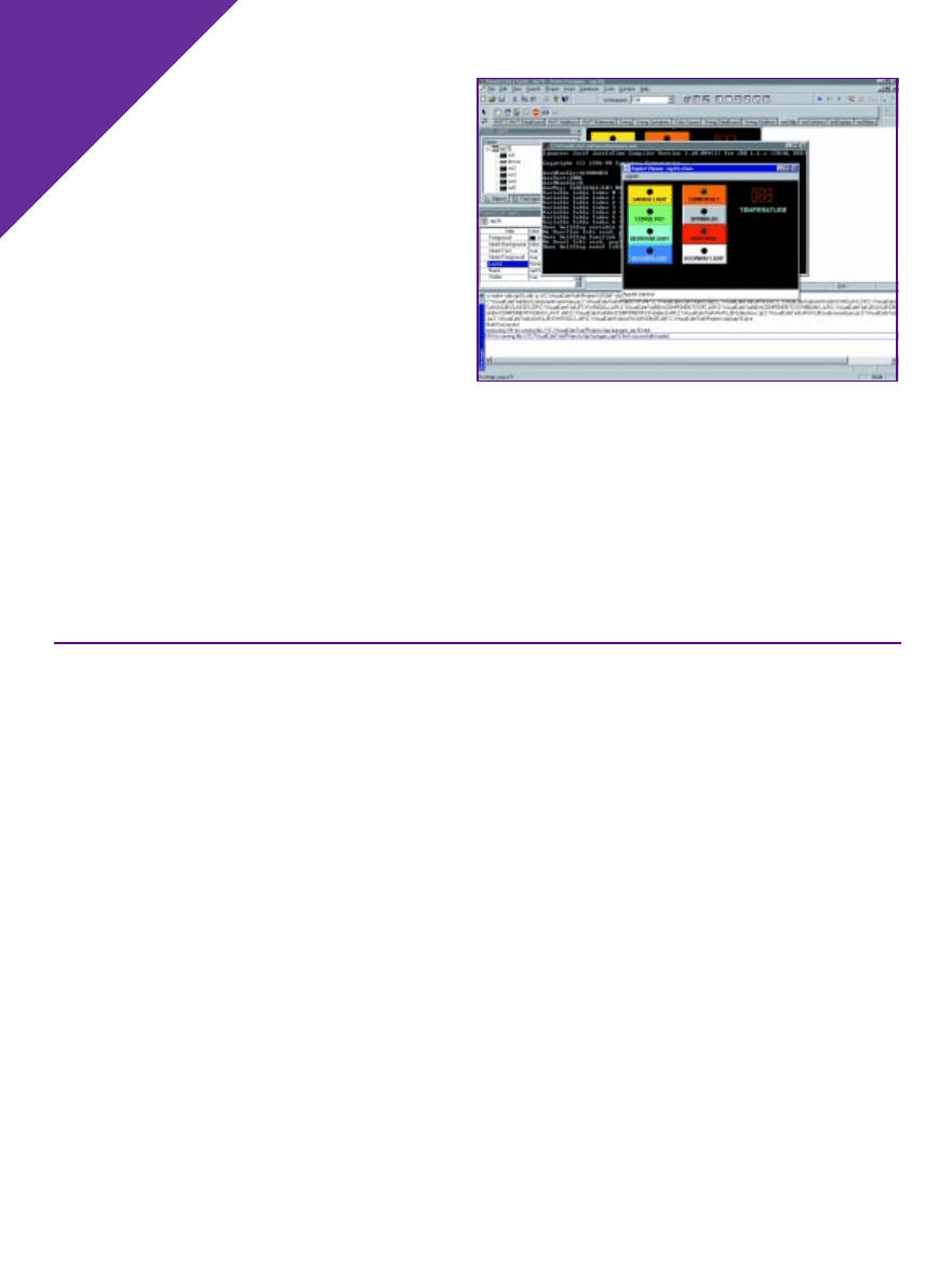
APC
CIRCUIT CELLAR FEBRUARY
2000
62
www.circuitcellar.com
doesn’t disappear before the editors can
get to it, you can see it in its raw form
(Visual Café applet mode) in Photo 5.
It wasn’t hard to put this together. It’s all
truly visual and you install the emObjects
when you go through the setup process for
EMIT. Although I have a bad taste in my
mouth for Visual Café’s trialware, I must
say that if you want to learn JavaScript on-
the-fly, Visual Café is much like Bill’s
Visual stuff in that it anticipates and cor-
rects when it can. I used this feature to
write some of the value manipulation
routines by hand. (Look, Ma, no manual!)
There’s too much code to show you in
one sitting, but I want to point out the
connecting lines of JavaScript. Those con-
necting lines are the key to seeing how it
all works together.
Listing 1 infers that TCP/IP is lurking out
there somewhere, too. Well, that’s one of
the things that make this virtual ’net work.
Photo 5—This is
quite busy but could
be a very powerful
tool if Symantec
would turn it loose.
Visual Café is the
only software that
is not truly free.
MAKE IT PRETTY
There are many ways
to effect the final user inter-
face. ActiveX, JavaScript, and
roll-your-own HTML are a few
methods I tried. I ended up using
JavaScript. Why? It was (kind of) free.
Symantec’s Visual Café Database Edition
is the package used in the tutorials and the
only package offered in the free down-
load area.
I’ll be honest. I think the Visual Café
download is too crippled to be of much
use as a demo here. It often loses its ability
to generate code and is not a pleasant
thing to integrate into the EMIT package.
I tried to use some of the bells and whistles,
only to be told I couldn’t. If it did let me, it
would sometimes fail to execute and tell
me I had violated security. The real killer
is that it goes dead after its trial period.
The good news is that the emWare code
is free for the asking after the trial period.
You simply send in your “I like it” request
via e-mail. (Bill, are you listening?)
Anyway, I managed to produce a
good-looking picture despite being chal-
lenged all the way by Visual Café. If it

63
www.circuitcellar.com
FEBRUARY
2000
E
MBEDDED
PC
Photo 6—Okay, so it’s
83° F outside. The little
black hole in each of the
switches is a status LED.
The SHOP HVAC LED is
green while all of the oth-
ers are red.
The line containing the reference to the
localhost and EMNET ties it all together.
The “localhost” is actually 127.0.0.1.
So, by entering http://localhost/
iapboard16/iap16.html as the URL, I get
the applet screen shown in Photo 5 on a
web browser. That’s assuming I’m on the
gateway machine and the localhost set-
ting is truly 127.0.0.1. Now, if I’m not on
the gateway machine and the gateway
machine’s IP address is set to 10.10.0.10,
and if the gateway machine is on my local
Ethernet LAN, http://10.10.0.10/
iapboard16/iap16.html will yield Photo 6.
Now it all makes sense, the virtual
Internet is really my wires connected to
emWare gateways connected to PIC EMIT-
enabled servers. The beauty of this is that
within a Microsoft Ethernet LAN environ-
ment using Win98 or WinNT, I can set up
dial-in configurations enabling me to dial
up the gateway or virtual router and specify
a URL to get to a device on the gateway.
Of course, I could also do this on a
LAN-connected host. A snippet of code
that shows how the PIC code is interlaced
with the EMIT code is shown in Listing 2.
GETTING ON THE VIRTUAL WEB
The groundwork has been laid. You
probably already have a virtual web in
your home or office. Now, what about
using the power of that PIC server at the
end of the chain?
As you see in Listing 2, it’s just a matter
of inserting your code in the right places
in the EMIT skeleton. The designer of that
code did a good job. It’s by far the best
example code I have ever seen. If you
can’t read, then you can call him at
emWare and he will explain to you just
how it works. How do I know that?
Hmmm….
But, before you sign on to your virtual
web, you have to get your golden code
into the PIC server IC. Behold, Photo 7. As
you can see, it loads, it reads, it pro-
grams, and it’s free! Never mind what’s
under the GUI you see, it uses the parallel
port of the iap16board to do things to the
PIC16F876’s program flash memory and
EEPROM.
I’ve been holding back. Did you notice
that Figure 1 shows a PIC16F877 and a
PIC12C67X? Well, that program GUI you
java.net.URL baseURL = getDocumentBase();
/* check if applet is loaded as a local file or served up by
emGateway */
if( baseURL.getProtocol().equals(file) ) {
/*applet is being loaded as a local file or by an applet
viewer.
emGateway must be running on the local host and the device
connected to COM1.*/
EmitJri.connect(emComUtils.initTCP(http://localhost/
EMNET.RS232+COM1/0/));
}
else {
/*Applet is served by an emGateway. Connection established
using document base.*/
EmitJri.connect(emComUtils.initTCP(baseURL));
Listing 1—I just wanted to show the link between the Java machine and the emWare
definitions.

CIRCUIT CELLAR FEBRUARY
2000
64
www.circuitcellar.com
;#define
__16C73
;#define
__16C73A
;#define
__16C73B
;#define
__16C74
;#define
__16C74A
;#define
__16C74B
#define
__16F877
The __16F876 entry was added to setup the config words and includes.
IFDEF
__16F876
LIST
p=16f876
include <P16f876.inc>
__CONFIG _LVP_ON & _BODEN_ON & _CP_OFF & _PWRTE_ON & _WDT_OFF & _HS_OSC
__IDLOCS H'1199'
ENDIF
IFDEF
__16C63
LIST
p=16c63
include <P16c63.inc>
__CONFIG ( _BODEN_ON & _CP_OFF & _PWRTE_ON & _WDT_OFF & _HS_OSC )
ENDIF
********************************************************************************
Here's where the variables are allocated.
;*******************************************************************************
; emAPP.asm - Allocate application variables.
;*******************************************************************************
CBLOCK
; Allocate application variables here.
Button
Leds
Ledport
Tempf
AARGB0
AARGB1
AARGB5
BARGB0
REMB0
LOOPCOUNT
TEMP
arg0
arg1
ENDC
********************************************************************************
This is the code for reading the A/D and computing the actual temp in degrees
Fahrenheit.
gettempf
banksel ADCON0
bsf
ADCON0,GO
gettingtempf
btfsc
ADCON0,GO
goto
gettingtempf
banksel
ADRESH
movfw
ADRESH
banksel
AARGB1
movwf
AARGB1
banksel
arg1
movwf
arg1
banksel
ADRESL
movfw
ADRESL
banksel
AARGB0
movwf
AARGB0
banksel
arg0
movwf
arg0
movlw
2
banksel
BARGB0
movwf
BARGB0
call
FXD1608U
banksel
AARGB0
movfw
AARGB0
banksel
Tempf
movwf
Tempf
return
Listing 2—Basically, I added the ’877 definition and inserted my unique code in the
designated places. The only requirement is that your code give up time for the EMIT code
to run.
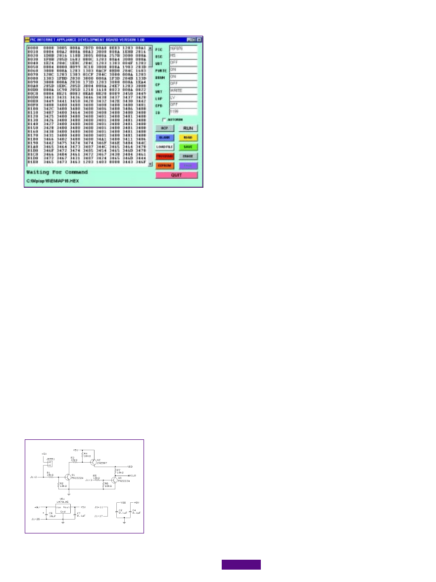
65
www.circuitcellar.com
FEBRUARY
2000
E
MBEDDED
PC
Fred Eady has over 20 years’ experience as
a systems engineer. He has worked with
computers and communication systems large
and small, simple and complex. His forte is
embedded-systems design and communica-
tions. Fred may be reached at fred@edtp.com.
see in Photo 7 can do both the ’876 and
the ’877. Just use the corresponding ’876
pins to build up the ’876 version. The
difference is that the ’876 is a smaller 28-
pin skinny package, has fewer digital I/O
pins, and lacks five A/D port pins compared
the ’877, but the rest is the same.
Here’s how the iap16board hardware
works. The MAX233 does standard serial
stuff. The 24LC256 is optional but neat to
have because the example code emWare
provides shows you exactly how to use it.
The 74LS125 is a buffer to disconnect the
PIC’s program lines from the parallel port
write port during read operations.
Notice there is no +13 VDC circuitry.
J1:4 controls the program mode and the
high voltage is generated within the
PIC16F876/877. Voltages are controlled
using parallel port pins directing transis-
tors Q1–Q3, and jumpers 1 and 2 allow
the disconnection of the parallel cable for
standalone operation (see Figure 2).
Write the PIC code using Microchip’s
MPLAB (which you can also get for free)
and you have the full virtual Internet pack-
age. emWare provides the connectivity,
Win9X provides the remote access, Mi-
crochip provides the server, Symantec
provides the user interface, and you pro-
vide the application.
At your disposal you have abundant
digital I/O (depending on your choice of
PIC processors), up to 10 channels of A/D
conversion, capability of remote access to
the digital I/O and A/D functions, an
embedded gateway that can be used for
other concurrent processes, and a private
addressable network structure.
LOGGING OFF
With minimal cash and some thought,
you can implement your own private
internet. The PIC devices have so much
I/O, you could deploy a single PIC server
in an area and control and monitor up to
15 digital I/Os and 10 analog inputs. If
you don’t need that much I/O, use the
baby PIC. As Led Zeppelin might say,
“The Code Remains the Same.” By the
way, the switches you see in the web GUI
individually control each PORTD I/O on
the PIC16F877 in any combination!
This technology is used at the largest of
companies and yet is available to us all.
Follow the little red ball. emWare recently
announced the addition of an Ethernet
DLM. If it’s not complicated and it’s em-
bedded, you’ll see it here.
APC.EPC
Photo 7—This is really a
full-blown serial PIC pro-
gramming package with
the fat trimmed to ac-
commodate the flash-
memory parts only.
Figure 2—The 13 VDC for programming is
generated within the PIC.

66
Issue 115 February 2000
CIRCUIT CELLAR
®
www.circuitcellar.com
1
2
Rapid Gratification
with FPGA Design
MICRO
SERIES
Tom Bishop
h
With cur-
rent tools
and the
technology of today’s
FPGAs, the process
of designing and de-
veloping systems is
getting easier and
faster. Don’t get left
behind. Listen up as
Tom gets us up to
speed on the topic.
ave you ever
wanted to proto-
type a design
quickly? What if you
could sketch a block diagram of a
fairly complicated system in the
morning, define, refine and simulate
the design during the afternoon, and
have working hardware by evening?
With today’s technology, it’s possible.
Computer tools are available from
field programmable gate array (FPGA)
vendors that enable you to quickly
develop systems. With these tools and
the modern design techniques they
support, a one-day development
project is within reach.
The software used to develop
FPGAs can seem complex. Indeed, the
number of new things to learn (e.g.,
software, internal structure of FPGAs,
and the new methodology involved)
can be daunting.
For many hardware designers, in-
timidation will prevent FPGAs from
being used at all. The companies that
supply the chips and the design soft-
ware understand this, and that’s why
ease of use has been a high priority.
Xilinx and Altera, the two leaders in
the field, have worked hard to provide
a pushbutton flow to the tools.
I’ve been experimenting with
quickly prototyping hardware using a
Xilinx FPGA demonstration board
that contains two FPGAs, switches,
displays, and support functions. The
results have been surprisingly good.
Also, taking an idea from concept to
working circuit in such a short time
is incredibly gratifying, not to men-
tion lots of fun.
One of my most recent experi-
ments involved a practical application
project. I live in a subdivision that has
a small water system that supplies
about 100 houses. I was helping set up
some new filters, and we found that
some of the equipment didn’t inter-
face very well.
The plant uses turbine meters in
the water mains to measure the total
flow. These meters have a tiny reed
switch that is momentarily closed
once for each gallon of water that
flows through the meter. The reed
switches connect to electronic con-
trollers that backwash the filters ev-
ery few hundred thousand gallons.
The controllers also display a flow
rate and other information used to
tune the operation of the plant.
The problem is that the controllers
are built to work with a much higher
flow rate than our plant can generate,
or with meters that produce many
pulses per gallon. We filter around 40
gallons per minute, which produces
about pulse rate at 0.7 Hz. The con-
troller datasheet indicates that we are
well within the pulse rate limits of
zero to 400 Hz. At this flow rate, the
controller alternates between two
values in its display—0 and 120 GPM.
This tells me that the controller is
counting pulses in a 0.5-s sample
period (1/120 min.), because there are
either 0 or 1 pulses in that time.
There are many possible ap-
proaches to solve this problem. The
best solution would be to fix the soft-
ware in the controllers. (There were
other software bugs that we discov-
ered, as well.)
I called the controller manufac-
turer and discussed the possibility of
fixing the software, but they had no
plans for any future software up-
grades. I even offered to fix the bug in
the ’68HC11 assembly language for
free, but they did not want an outsider
to view their code. If the cryptic
manuals that came with the control-
Getting Up to Speed
Part
1
2
of
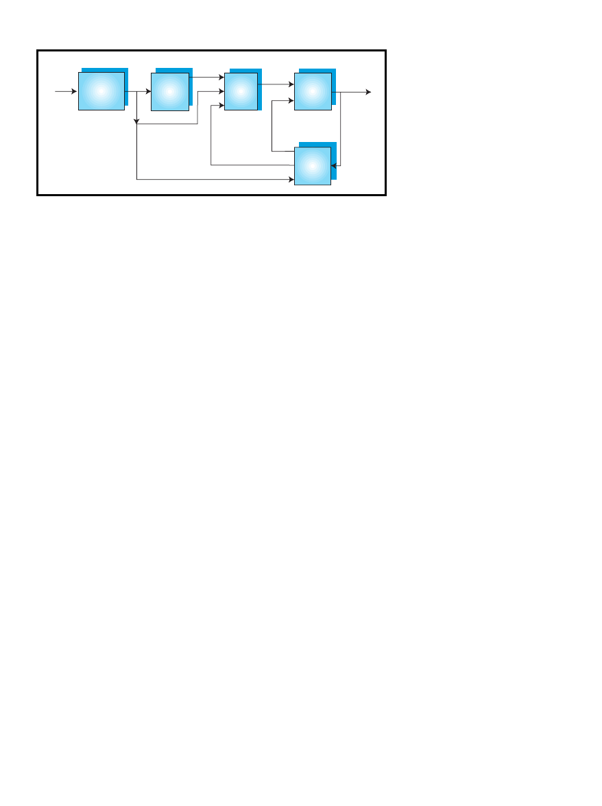
CIRCUIT CELLAR
®
Issue 115 February 2000
67
www.circuitcellar.com
lers are any clue, I’m probably fortu-
nate that they didn’t accept my offer.
The pulse multiplier was designed
to make the flow meter operate prop-
erly. My goal was to make a simple
piece of hardware that could take in a
low-rate pulse stream and produce a
multiple of the input frequency (see
Figure 1). I can change the scale factor
in the controller to cope with a differ-
ent number of pulses per gallon. By
producing enough pulses in each 0.5-s
sample period, we could then display
a good, and fairly accurate flow rate
on the display.
The circuit must be able to respond
to contact closures at a frequency of
0.1–3 Hz, and it must produce some
integer multiple of evenly spaced
pulses at the output. Also, the total
count of output pulses is important
because the controller is recording the
total flow through the filters. No
matter how the input rate changes,
the circuit must produce the exact
multiple of output pulses—no more
and no less.
How can a circuit multiply the
input frequency? As with most engi-
neering problems, there are many
possible solutions. You might use an
analog phase-locked loop. But, the
ratio of input frequencies is 30:1,
which is wider than the lock range of
most PLLs. Besides, my expertise is
more digital than analog.
An approach that appealed to me
was to measure the input pulse width,
then set a counter to cycle at a mul-
tiple of that rate. By using a local
clock with a relatively high fre-
quency, we could count clock cycles
between two input pulses, load an-
other counter with a fraction of that
number, and then allow it to count
down. When the second counter
reaches zero, we toggle the output,
reload the counter, and repeat.
For example, suppose we want to
multiply the incoming pulse rate by
10. We would divide the input count
by 20 because we need to toggle twice
to produce a full cycle of output. If
the circuit counted 600 clock cycles
between two input pulses, it would
load an initial value of 30 into the
output counter. The output counter
would count down to zero, then re-
load the starting value.
Each time we reload the counter,
we would toggle the output value. If
the flow remained consistent, we
would toggle the output 20 times,
producing an even pulse stream at 10×
the input rate.
I decided on an even better algo-
rithm than just a simple counter. A
line drawing algorithm used in com-
puter graphics is an integer digital
differential analyzer (integer DDA).
This algorithm attempts to draw a
line on a computer screen by drawing
a pixel at each point along the longer
axis. At each point, it looks at the
accumulated error to decide whether
to increment the position on the
shorter axis as well. This method can
be used as a multiplying operation.
We can consider the number of
clocks between input pulses to be the
longer axis and the desired number of
toggles to be the shorter axis. At each
clock tick, we can then decide
whether or not to toggle the output.
The result is that we can generate an
arbitrary number of toggles in what-
ever number of clock ticks we want,
without any round-off errors or loss
of precision.
This is convenient for another
reason. We need the multiplier to
produce an exact multiple of the in-
put pulses. If the flow rate is increas-
ing, the duration between input
pulses will be decreasing. Unless we
apply a correction, we will consis-
tently produce less toggles than we
require. Our total capacity measure-
ment would be wrong.
We’ll restart the DDA when after
detecting each new input pulse. At
that time, we can add the number of
toggles that remain for the previous
input cycle. The integer DDA lends
itself to this application. The simple
down-counter approach described
would require a general-purpose di-
vider or other method to apply error
corrections, which would greatly add
to the total circuitry.
The requirement to produce an
exact multiple of input pulses works
the other way, as well. After we gen-
erate the multiple of input pulses, we
have to stop the circuit from toggling,
even if new incoming pulses do not
occur. A counter that detects toggles
on the output, and inhibits the rest of
the circuitry can provide this function
and resolve the issue.
THE DESIGN ENVIRONMENT
Now that the system architecture
is specified, let’s capture the design.
The design environment and setup
used to bring this design to fruition
were the most exciting parts of the
project for me.
There are a number of ways to
capture a design. This project was a
mixture of schematic sheets and
VHDL text files (for more information
on VHDL, see the “What is VHDL”
sidebar). Another project might cap-
ture part of the design as state ma-
chines diagrams.
Most designers are used to entering
a schematic into a computer as the
basis of a design. The schematic is
then used to generate a net list that is
used as the main source file. For me,
schematic generation was always a
fun part of the design process. Gener-
ating the schematics is the main inte-
Figure 1—
This is the block diagram of the pulse-multiplier circuit. The input is a low-frequency pulse train. The
output pulse train will have an exact multiple of the number of input pulses.
Input
pulse
Edge detector
Start
Counter
DDA
multiplier
Toggle
Output
generator
Hold
Error
Error
accumulator
Output
pulse
Input
duration

68
Issue 115 February 2000
CIRCUIT CELLAR
®
www.circuitcellar.com
What is VHDL?
VHLD is an acronym for VHSIC hardware description language.
VHSIC is in turn an acronym for very high-speed integrated cir-
cuit. Engineers like acronyms, but even engineers generally don’t
stack them two layers deep!
VHDL is a special language developed under contract for the US
Air Force so a circuit could be described in a precise language. The
VHDL description would then specify exactly how that circuit
should operate. When technologies became obsolete, devices were
redesigned that would match the functionality of their predeces-
sors. With long life-cycle products, redesignability was an impor-
tant requirement.
How is VHDL different from most computer languages? Most
languages enable us to efficiently write code that is easily readable
by a human, and is at a high level. A compiler or interpreter can
then translate that code into machine instructions. VHDL is also
meant to enable us to write at a high level.
Instead of being designed for easy translation into machine
language, VHDL is designed to accurately model logic circuits.
One key difference is that with a computer program, the order in
which the instructions are executed is precisely known. With a
logic circuit, each gate reacts whenever its inputs change and
there is no clear order of operations. This method is called concur-
rent processing, which means that gates are all operating at the
same time. The ability to model the function of a concurrent cir-
cuit is a fundamental characteristic of the VHDL.
VHDL was designed as a language that could be simulated in a
computer. A simulator could execute the model, and a user could
observe the circuit’s operation. This enables you to operate, de-
bug, and modify your design before ever touching hardware.
VHDL is a high-level language (i.e., complex circuits can be
designed efficiently). VHDL can model logic gates. You might find
it useful to model some logic gates as a tool to learn about the
language. Otherwise, almost all design work with VHDL will be
done at a higher level.
For instance, assume we have three buses (A, B, and C) that
carry values and we want to add them together. Typing D <= A + B
+ C would assign the result to the bus called D and spare you
most of the tedious details of this operation.
VHDL was originally used as an executable specification for a
design. Logic circuits would then be designed to perform the
specified functions. If the logic circuit and the VHDL model pro-
duced the same outputs for every set of inputs, the specification
was satisfied.
Sometime after VHDL was designed, computer tools were de-
signed to synthesize a gate-level logic circuit directly from a
VHDL description. This revolutionary step enables designers to
write, debug, and verify a VHDL model, then instantly convert
that model into gates.
That design process results in a high level VHDL model that
humans can read and (hopefully) understand, a simulation of the
VHDL model to demonstrate and verify the circuit operation, and
a gate-level net list that can be easily implemented.

CIRCUIT CELLAR
®
Issue 115 February 2000
69
www.circuitcellar.com
gration step for turning the block
diagram into working circuitry.
After designing the schematic,
there’s generally a PCB design and
fabrication step that takes a month or
more. If a design is urgently needed,
this cycle could be shortened to about
two weeks before testing could begin.
Using the FPGA demo board, a
schematic can be turned into a work-
ing circuit in minutes and you can
start the debug process. The resulting
design can be downloaded into the
FPGA demo board, inputs and outputs
connected as needed, and then tested.
Insight Electronics now sells a set
of prototyping boards with up to 300k
gates on a single chip. The demo
board I used is available from Xilinx
for $350 and demonstrate the ease of
design of Xilinx FPGAs. It contains
PLCC sockets for two FPGAs (one
each of the 4003E and older 3020A
devices), dip switches for program-
ming configuration and user-defined
functions, 16 LEDs, three 7-segment
displays, and three pushbuttons.
There are also header strips that con-
nect to each pin of the FPGAs for
connection to external logic analyzers
or other circuitry. Lastly, there is a
prototype area, with a 24 × 35 plated
holes on 0.1
²
centers. For the fre-
quency multiplier, I used only the
displays and pushbutton switches, as
well as connecting test equipment to
the header strips.
In operation, you complete a design
as any mixture of schematic sheets,
VHDL or Verilog files, and state-ma-
chine diagrams. Most of the opera-
tions to compile and download a
design from the Xilinx computer tools
are performed with a mouse click
from the GUI. Synthesis, optimiza-
tion, and place-and-route operations
all occur with a single button push.
With the pulse-multiplier design,
those three steps take around 40 s on
my PII-450 computer.
Next, you connect an adapter from
a serial or parallel port on your com-
puter to a pair of header strips on the
demo board. Another button push
downloads the design from the host
computer to the demo board. It takes
between one and four seconds to
download a design. As soon as the
70
Issue 115 February 2000
CIRCUIT CELLAR
®
www.circuitcellar.com
SOURCES
FPGAs
Xilinx, Inc.
(408) 559-7778
Fax: (408) 559-7114
www.xilinx.com
Altera Corp.
(800) SOS-EPLD
(408) 544-7000
Fax: (408) 544-6403
www.altera.com
ModelSim
Model Technology, Inc.
(877) 435-4255
(503) 641-1340
Fax: (503) 526-5410
Tom Bishop has been a design engi-
neer for 18 years, specializing in
FPGA and ASIC design and verifica-
tion using VHDL and Verilog. As a
consultant for nine years, his larger
projects have involved computer
graphics, video, telecom systems,
processors, PCI and FireWire busses,
and customer training. You may
reach Tom at tbishop@asiccess.com.
download completes, the circuit is
reset and placed into operation.
The price of the design environ-
ment varies depending on the features
required. Xilinx sells a schematic-only
base package that works with designs
of up to 10,000 gates for $95. Adding
VHDL synthesis to these features
brings the price to $495. The full
package for all parts with VHDL syn-
thesis is $4995. These prices include
only gate-level simulation.
I think a behavioral simulator is
necessary and have used Model
Technology’s ModelSim product ex-
tensively. I also have Aldec’s Active
VHDL simulation environment,
which is similar, but adds a few fea-
tures. Both of these products cost
around $4000. The cost might seem
high, but they’ve paid for themselves
many times over. Not to long ago, a
simulation and synthesis design envi-
ronment on a workstation cost well
over $100,000.
In part two of this article, I’ll take
a detailed look at the steps involved
in FPGA design and programming.
I
Active VHDL
Aldec, Inc.
(800) 487-8743
(702) 990-4400
Fax: (702) 990-4414
www.aldec.com
NEW TO FPGAs?
With programmable logic devices be-
coming more common among designers, we
want to provide you with the information
you’ll need to keep up with the technology.
That’s why we introduced a bimonthly
column in
Circuit Cellar Online that focuses
on FPGAs and CPLDs. Who better to pro-
vide the information than
Circuit Cellar
columnist Ingo Cyliax, who discovered the
benefits of FPGAs long before they were
considered mainstream.
The first two articles in the Learning the
Ropes column provide a background tour of
FPGAs. You’ll find
Circuit Cellar Online under
the Ezines button at www.chipcenter.com and
from there all you have to do is take a look at
the archived articles from November and
January and you’ll be ready to use FPGAs in
your next design project.
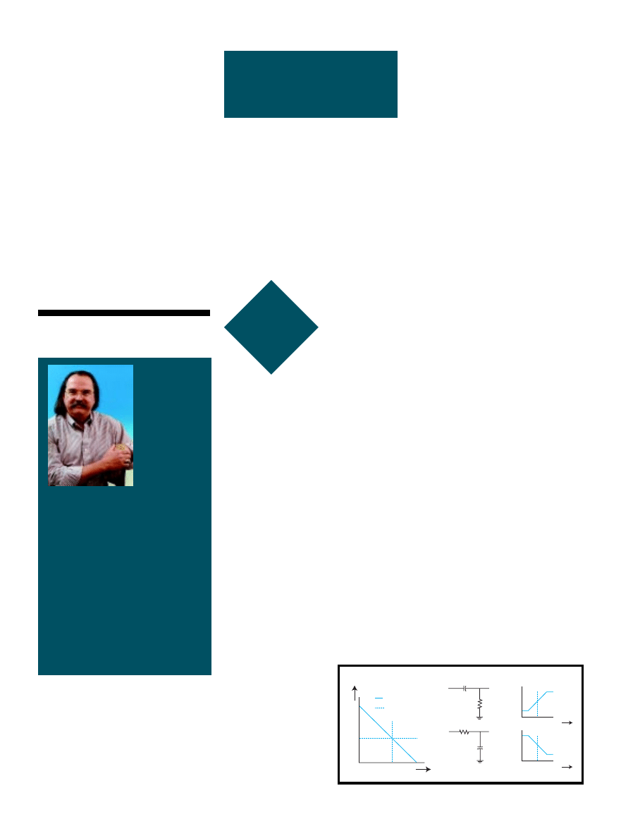
72
Issue 115 February 2000
CIRCUIT CELLAR
®
www.circuitcellar.com
FROM THE
BENCH
Jeff Bachiochi
In Theory and in Practice
This
month,
Jeff
starts
off with
a bit of filter theory
and before long
he’s designing a
clock-tunable digital
filter using Linear
Technology’s
LT1068.
never thought
of filtering as
something I con-
stantly use. However,
after a bit of thought, I realized that
without filtering, our lives would be
even more confusing than they are
already.
Certainly the news would extend
beyond the usual half hour if someone
weren’t responsible for filtering out
all but the top stories. Food shopping
would be much more difficult if the
grocer didn’t keep the number of
manufacturers to a minimum. Radio
and TV would be unintelligible if
filters weren’t used to separate station
reception. Our drinking water is fil-
tered to remove all sorts of matter,
improving both taste and, in some
instances, smell.
All sorts of filtering is taking place
in the backgrounds of our lives. I
guess I’ve taken it for granted. In elec-
tronics, filtering is one of the most
basic needs. It seems as if there are
always signals we want to eliminate.
For years, the only way to do this was
with a passive analog filter.
Passive analog filters are comprised
of one or more frequency-dependant
components. They come in two basic
varieties—the low-pass and high-pass
filter. The simplest filter is a resistor/
capacitor divider.
Refer to these two first-order (num-
ber of active components) configura-
tions in Figure 1. Notice how only the
capacitor’s impedance changes over
frequency. The frequency at which the
impedance of the capacitor and resis-
tor are equal is considered the F
c
(cut-
off frequency). The impedances of
each device are the same at the cutoff
frequency, so therefore both circuits
have an equal affect on an input of F
c
.
The output of each circuit will be
0.707× the input. But, all of this
changes with a shift in frequency. As
the input frequency goes up, the im-
pedance of the capacitor goes down at
a fixed rate of the inverse of the fre-
quency change (C
IMP
=
1
¤
2
p
FC). This
amount of change is 6 dB/octave.
You can see that in the two circuits
in Figure 1, as the frequency (and
capacitor’s impedance) changes, the
effect on each of the dividers is oppo-
site. As frequency increases above F
c
each of the capacitors will experience
a lowering of its effective impedance.
In the high-pass circuit, the lower
impedance has the affect of raising the
output above F
c
. In the low-pass cir-
cuit, the lower impedance has the
affect of lowering the output below F
c
.
These circuits are passive because
their output will always be lower than
their input.
Inductors can be used in filters as
well as capacitors. Inductors have the
opposite characteristics of capacitors.
Part 1: Digital Filters
Figure 1
—As frequency
changes, a capacitor’s imped-
ance also changes while a
resistor’s impedance (resistance)
remains constant. The point
where these values are equal is
considered the cutoff frequency.
This is the frequency where the
component with the major
influence will shift to a minor
influence.
i
0
Frequency
I
m
p
e
d
a
n
c
e
Capacitor
Resistor
In
Out
In
Out
High pass
O
u
t
p
u
t
0 Frequency
O
u
t
p
u
t
0 Frequency
Low pass
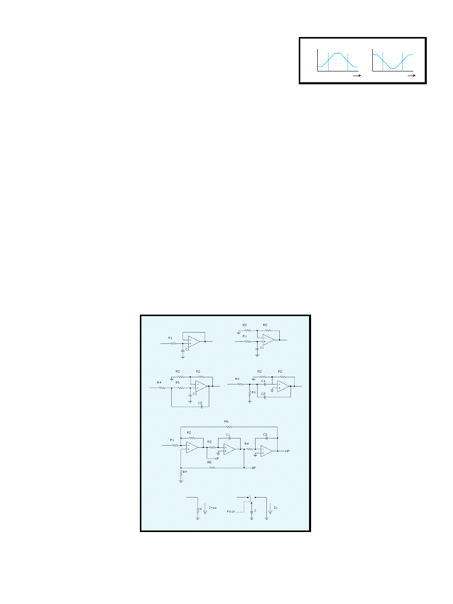
CIRCUIT CELLAR
®
Issue 115 February 2000
73
www.circuitcellar.com
filter to provide buffering. This non-
inverting arrangement also offers the
advantage of providing gain by replac-
ing the feedback path with a resistor
pair, as in Figure 3b.
Second-order filters can also be
formed with a single op-amp, as
shown in Figure 3c. This configura-
tion has a 12-dB/octave transition
slope. To produce higher than second-
order filters, multiple filter stages
must be used. Designing a third-order
filter using a single op-amp has stabil-
ity concerns because the resulting
phase changes can create reinforcing
oscillations.
As I mentioned earlier, low- and
high-pass filters can be combined to
produce band-pass or band-reject fil-
ters. It’s possible to combine these
into a second-order (single pole)
single-op–amp band-pass (or
band-reject) filter. In this con-
figuration, the filter sections
are split into a single-order low-
pass and a single-order high-
pass filter (see Figure 3d). The
resultant slopes will be
1
¤
2
of
second-order low-pass or high-
pass filter, or ±6 dB/octave.
A variation on the second-
order filter, which uses three
op-amps, is the state variable
filter. This configuration (see
Figure 3e), while using multiple
op-amps, offers simultaneous
outputs of low-pass, band-pass,
and high-pass. An offshoot of
the state variable filter is the
active-switched capacitor filter,
which uses switched capacitors
to simulate internal resistors.
These capacitors are switched
via an external clock at a rate of
25–200× that of the filter’s cen-
ter frequency.
The charging and discharging
of the capacitor simulates the
current flow through the substi-
The phase change for these circuits
is based on frequency. The low-pass
filter’s output phase change will begin
at about zero below F
c
, lag by 45° at
F
c
, and approach a lag of 90° above F
c
.
The high-pass filter’s output phase
change will lead by about 90° below
F
c
, lead by 45° at F
c
, and approach zero
above F
c
.
Because of the resistive component
in the above passive example, the
phase change is not linear with re-
spect to the frequency change. There-
fore, the
D
phase/
D
frequency or group
delay is not a constant.
Without getting into a discussion
of poles and zeros in the filter’s trans-
fer function, I’ll just say that adding
poles increases the steepness of transi-
tion regions and also increases the
oveall group delay. The placement of
the poles on the complex plane affects
both the linearity of the phase re-
sponse and the amount of ripple in the
passband.
ACTIVE FILTER TRADEOFFS
Referring to Figure 3a, an op-amp
can be used with a first-order passive
Although inductors are not necessar-
ily more expensive than capacitors,
the capacitor is the component of
choice for most filters. There is also
some resistance associated with in-
ductors, which is not affected by fre-
quency yet must be taken into
account. For the purpose of this col-
umn, I will be using only capacitors.
When the filtered output must not
be attenuated (reduced), an amplifier
is used to raise the output back up to
the required level. Transistors were
the first active circuits to be used as
filter-gain stages. However, with the
introduction of op-amps, active filters
began taking on unique configurations.
BUILDING BLOCKS
The low- and high-pass filter con-
figurations can be combined to create
other useful circuits. Refer to Figure 2
to see how these can be combined to
produce both band-pass and band-
reject configurations. Note that both
new configurations have multiple F
c
s.
There are a few terms that are
important to know and are used to
more technically define filters (see
Figure 4). The passband is the
group of frequencies that is
permitted through the filter.
The amplitude deviations
within the passband are called
passband ripple. The stopband
is the group of frequencies that
are considered rejected or at-
tenuated by the filter.
Between the passband and
the stopband is an area known
as the transition band. The
transistion slope is determined
by the configuration of the
filter. Referring back to
Figure 1, notice the slope of
this first-order passive filter is
6 dB/octave.
Up to this point, I’ve only
mentioned gain alterations as a
result of frequency changes
through a filter circuit. There
are also phase changes that
take place. The resistors in
Figure 1 don’t affect the phase
of the signal, however, the
frequency dependant capacitors
will add or subtract a phase
transition about F
c
.
Figure 2
—By combining low-pass and high-pass filters,
band-pass and band-reject filters are created. The F
c
s
of each filter determine the filter type.
Band-pass
Output
0
Frequency
0
Frequency
Band-reject
Output
Figure 3a
—Op-amp buffer isolates changing impedance. b—Op-amp with
gain compensates for passive filter loss. c—Second-order filter has 12 dB/
octave. d—High-pass and low-pass filters combined to produce band-pass
filter. e—State variable filter offers multiple filter outputs. f—Switched capaci-
tor filter uses a capacitor as a variable resistor.
a)
b)
c)
d)
e)
f)
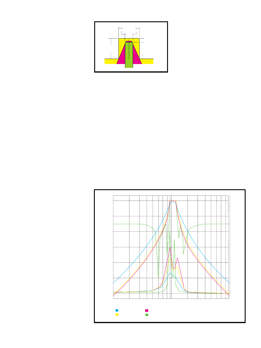
74
Issue 115 February 2000
CIRCUIT CELLAR
®
www.circuitcellar.com
tuted resistor (see Figure 3f). By using
CMOS switches on each end of the
capacitor, the charge on the capacitor
can be inverted as necessary in the
state variable filter implementation.
Note that if the clock frequency is
changed (effectively altering the “R”
associated with the F
c
calculation),
the center frequency of the filter is
proportionally moved.
The Linear Technology LTC1068
has four such universal filter blocks
within a single package. The device
can be operated from dual 5-V sup-
plies or a single 5- or 3.3-V supply. A
master clock input provides center
frequency tuning to all blocks. Each
block can be configured in a number
of modes that offer specialized func-
tions such as notch or all-pass.
Linear Tech offers FilterCAD soft-
ware to help design your own particu-
lar filter. Not only does this software
take you step by step through choos-
ing the appropriate parameters, it also
graphs the resulting response curves.
Even if you aren’t designing a filter,
it’s a great educational tool for explor-
ing what-ifs.
DEFINING PARAMETERS
For this project, I’m looking for a
fairly narrow low-frequency band-pass
filter. Let’s take a look at how this
would be specified. The first decision
has already been made—I’ll need a
band-pass filter.
Next, I need to indicate the center
frequency (F
c
) of the filter. This design
needs to pass frequencies around
10 Hz, so the design will use 10 Hz as
the F
c
. The next parameter to deter-
mine is the passband width (i.e., the
frequency extremes above and below
F
c
) that will also be passed.
Because the filter has a transition
band between passing and rejecting
Figure 4
—Filter designers must consider certain
parameters to properly define any filter.
Figure 5
—Here are some filter responses and their respective group delays.
Passband
ripple
Stopband
Passband
Stopband
attenuation
F
C
0db
–20db
–40db
–-50db
–80db
–100db
–110db
1Hz
10Hz
100Hz
1.2s
1.0s
0.8s
0.6s
0.4s
0.2s
0.0s
Bessel
Butterworth
Chebychev
Elliptical Filter
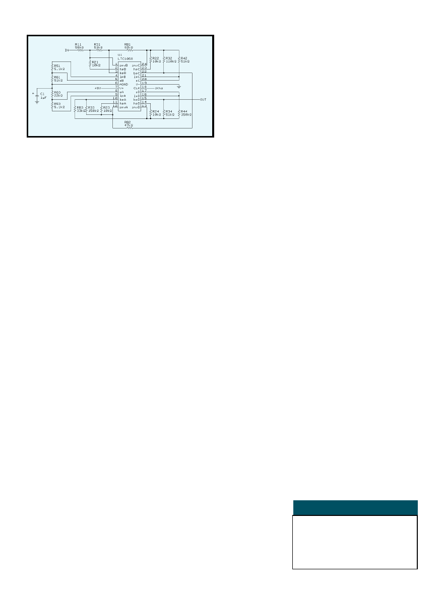
CIRCUIT CELLAR
®
Issue 115 February 2000
75
www.circuitcellar.com
Figure 6
—Four second-
order filter blocks are
contained within Linear’s
LTC1068. The clock input
sets the filter’s center
frequency.
Jeff Bachiochi (pronounced“BAH-key-
AH-key”) is an electrical engineer on
Circuit Cellar’s engineering staff. His
background includes product design
and manufacturing. He may be reached
at jeff.bachiochi@circuitcellar.com.
SOURCE
LT1068, FilterCAD
Linear Technology
(408) 432-1900
Fax: (408) 434-0507
www.linear-tech.com
unwanted frequencies, there must be
some reference point to indicate the
extremes of the passband, which are
independent of the transition slope.
This –3-dB reference point is where
the output of the filter drops to 50%
of the input. I would like this to be a
fairly narrow band so I’ll use 4 Hz
(±2 Hz) as the passband width.
Now comes the interesting param-
eter—establishing the transition band.
The transition band is the slope of the
transition area and is defined by the
stopband width at a given attenuation.
The stopband width is similar to
passband width. Frequency extremes
above and below the F
c
will be re-
jected. Unlike the passband, the
stopband doesn’t have a fixed dB point
associated with it. With the passband
frequency limit (at the –3-dB point) as
the upper point of a slope and the
stopband frequency limit (at the user-
provided stopband attenuation point)
as the lower point of a slope, you can
now visualize a frequency plot of the
filter (see Figure 4).
After looking at Figure 4, you
might think that the stopband fre-
quency and attenuation level might
actually be designated anywhere along
the slope. That is somewhat true, but
notice that the floor of the design
frame would move up as the stopband
attenuation point is reduced.
Although we think of filters as
having transition regions that extend
and attenuate infinitely, there are
designs that attenuate only to a spe-
cific level. So, the stopband attenua-
tion level designates the filter’s floor.
DESIGNING WITH FilterCAD
Because I’m using the entire
LTC1068 for this filter, I want to
adjust the filter parameters to get the
best possible use from its elements.
The four second-order filters will be
cascaded to give the best eighth-order
flat response band-pass filter possible.
Although the FilterCAD software
has a quick design feature, some pa-
rameters can not be altered in this
mode. I chose to use the enhanced
design mode, which gives a user more
control over which parts and filter
response is used. The four basic filter
responses are Bessel, Butterworth,
Chebychev, and Elliptic.
Although each filter will have the
same transition rate (dB/octave), the
initial steepness of the transition
region is different for each filter. The
shape of the filter’s transition region
is a trade-off between transition rate
and passband ripple. While a flat pass-
band and gradual rolloff are typical of
the Bessel filter, the Chebychev filter
trades quicker rolloff for ripple in the
passband.
Because most real-world filters
have dynamic input signals, a filter’s
phase response may be of importance.
In general, heavy damping gives linear
phase response. The filter’s transient
response characteristics are quantifi-
able as group delay (
D
phase/
D
frequency). Here a linear phase re-
sponse will be a constant. The trade-
off is linear phase response for quicker
rolloff.
Figure 5 shows each of the four
filter responses and their respective
group delays. Note that the design
criteria were adjusted for each of these
filters to maximize the abilities of the
digital filter for each type of filtering
method.
Figure 6 shows the filter I chose to
prototype. The FilterCAD program
creates a schematic complete with
component values at either the actual
or closest standard value. In testing
the filter, I found it to be quite close
to design specs.
The clock noise (feedthrough) I
measured with my scope was down in
the mud, about 1 mV or so. The
datasheet states 0.1 mV @ 1 MHz
using a bipolar 5-V supply. Consider-
ing the use of a unipolar supply and
the open construction I’ve used for the
layout with no ground plane, this
doesn’t surprise me.
WHY DIGITAL?
Certainly this filter could have
been constructed using op-amps and
discretes. In fact, FilterCAD will give
you the F
c
and Q factors for each stage
of a filter design. With these numbers
available, you can work through all of
the equations necessary for designing
an analog filter with the same result-
ant response.
In my case, there’s a good reason
for using a digital filter. If the answer
I’ve hinted at here isn’t obvious to
you, don’t worry, it will become so
next month, when I add a few compo-
nents on either side of the filter.
In any event, you probably have
and will most likely continue to use
filters in many of your designs. Al-
though active filters can be complex
in their theory, they are all based on
fundamental passive filters. So, don’t
get too excited when filter design
becomes necessary. If you can desig-
nate the parameters needed for your
design, you’ve already won. Whether
it be textbook equations or filter-
design software you seek, there are
plenty of tools available for assisting
with filter design.
I
76
Issue 115 February 2000
CIRCUIT CELLAR
®
www.circuitcellar.com
n
o doubt, and
quite fitting, that
2000 is the year the
embedded Internet really
starts gathering steam. Yeah, the PC
makes a great terminal for e-com-
merce, web surfing, and such, but
there’s so much more neat stuff to do.
Those of you who follow Circuit
Cellar Online
recall November’s SU
Online, in which I reviewed develop-
ments at the second annual Embedded
Internet Workshop— notably, the
emergence of a crop of under-$100
solutions to webify an embedded app.
Now, if you’re working for a
bigshot OEM on a brand new design
and have a huge engineering staff and
budget, it may be worth rolling your
own ASICs, using a
commercial
(RT)OS, TCP/IP
stack, and so on.
But what if you’re a
little guy, without
the means or will
to embark on a huge engineering exer-
cise? What if the product is relatively
low-volume and you’re less concerned
about squeezing every penny out of
the cost than the fact you needed it
yesterday.
What the world, or at least the
little guy, needs is a relatively low
cost, but quick and easy way to retro-
fit basic Internet functionality onto an
existing design. The silicon wizards
hear this plea and are concocting the
needed chips even as we speak.
The latest, and a good example, is
the iChip from ConnectOne. Priced at
$25 in quantities of 1k, it’s more proof
that double-digit (versus triple-digit)
pricing for embedded Internet solu-
tions is where the action is.
Before I get under the hood, let me
observe that most of the embedded
Internet excitement seems to revolve
around web servers. However, I per-
sonally think another option—e-
mail—hasn’t received the
consideration it should.
The web-server approach has ad-
vantages and disadvantages. Pros in-
clude the graphical interface for
handling hundreds or thousands of
browsers at a time and (in the case of
a full-blown client and server setup)
the ability to extend functionality
with tools like Java and XML.
However, the web-server approach
does incur costs as a result of hard-
ware and software complexity. Fur-
thermore, the strengths may not be
compelling, or may in fact be weak-
nesses. For instance, is there any rea-
son you’d want to give thousands of
EZ-Mail Engine
While
much of
the
embedded
internet
buzz focuses on web
servers, everyone is
ignoring a far more
cost-effective
solution— e-mail
capabilities. Stop
surfing for a second
and read on.
SILICON
UPDATE
Tom Cantrell
Figure 1
—The iChip from
ConnectOne is a black-box
e-mail engine that packs a
CPU, flash memory, RAM,
as well as host and modem
ports into a 68-pin PLCC
form factor.
CPU
core
Internal flash memory
128K x 16 or
256K x 16
Internal RAM
128KB x 8
Three 16-bit
timers
Interrupt
controller
DMA
controller
WDT
Local b
us interf
ace unit
UA
R
T
U
A
R
T
with
auto tr
ansf
er
Local address
bus 20 bit
Data bus
16 bit
WR
RD
Rx,Tx,
CTS,RTS,DTR,DSR,
RI,CD
Rx,Tx,
CTS,RTS,DTR,DSR,
RI,CD
RAM expansion
CS

CIRCUIT CELLAR
®
Issue 115 February 2000
77
www.circuitcellar.com
WWW users simultaneous access to
the innards of a vending machine?
By contrast, e-mail is a much
leaner and meaner solution, especially
when the audience is (or should be)
limited. Unlike HTML, simple status-
and-control information can be con-
veyed in a few bytes of ASCII. Less
complexity and eye candy streamlines
the required platform at both ends of
the wire. Witness the emergence of e–
mail-capable pagers and phones while
a web setup (at least one compatible
enough to be useful) calls for a lot
more intelligence, bandwidth, and a
high-resolution display.
Consider the vending machine
example. Let’s say it monitors itself
for problems such as temperature out
of range and reports any difficulties to
headquarters. Yes, it would be lovely
to have a web page with an animated
view of the vending machine ther-
mometer, unless the extra hardware
and software costs mean you don’t get
a raise. Me, I can live with a short and
sweet “Machine XYZ reports temp
out of range” message in my mailbox.
From the embedded perspective,
another nice thing about e-mail is its
send-and-forget nature.
Presuming the embedded
app has something better to
do besides serve up web
pages, it raises a latency
issue much like the differ-
ence between polling and
interrupts. To wit, the app
would have to refresh the
web page often enough to
convey information in a
timely manner. For e-mail,
a message can be sent at
the convenience of the app and need
only be sent once.
MAIL CALL
The bottom line is that it would be
great to have a basic e-mail add-on
that minimizes up-front engineering
effort and runtime silicon and software.
Enter the iChip which, as shown in
Figure 1, incorporates a ’186, 128K ×
16 or 256K × 16 flash memory for the
internal program and parameter stor-
age, 128K × 8 RAM for data and both
host-side (i.e., your app) and ’Net-side
interfaces. There’s also a local bus
comprising a 20-bit address bus and a
16-bit data bus for external memory
expansion if necessary. In the current
version, the iChip is basically a black
box that sits between your app and a
modem.
The host-side interface is a serial
port that includes the usual handshak-
ing lines (RTS, CTS, and DTR) and
handles transfer rates between 300
and 115.2 kbps. The modem-side in-
terface comes in serial and parallel
versions (see Figure 2). In essence, the
iChip looks like a serial modem to
hardware. The clever thing about the
concept is that it looks like a serial
modem to software, too.
The iChip has four modes of opera-
tion. In Transparent mode (the default
Figure 2
—Two versions of the iChip are available that differ only in
their incorporation of either (a) serial or (b) parallel connection to the
modem.
Embedded
CPU (host)
Serial
iChip
Serial
Data
modem
Tel.
Embedded
CPU (host)
iChip
Data
modem
Tel.
D0-7
A0-2
Serial
RD
WR
IRQ
CS
a)
b)
AT+i
I/OK
AT+iISP=9,4357701
(Number to dial)
I/OK
AT+iUSRN=someuser
(Account)
I/OK
AT+iPWD=ApassWord
I/OK
AT+iDNS=192.15.201.55,192.15.201.101
(Major, minor DNS)
I/OK
AT+iSMTP=mail.domain.com
(SMTP server name)
I/OK
AT+iXRC=0
(Blind dial)
I/OK
AT+iTOA=sombody@domain.com
(Define recipient address)
I/OK
AT+iFRM=iChip@domain.com
(Define originator address)
I/OK
AT+iTOA~onetimeaddress@somewhere.com
(Temporary recipient)
I/OK
AT+iSBJ~Hello form iChip
(Temporary subject)
I/OK
AT+iEMA:These characters will be sent in
(E-mail body)
the email body. Intervening CR/LF characters are allowed
to format the lines of the e-mail. The maximum number of
characters allowed in a single e-mail transmission is 96 KB.
.
(Terminator line)
I/OK
AT+iRP2
(Request status)
Connecting to ISP
AT+iRP2
Establishing SMTP connection
AT+iRP2
Sending message
I/DONE
(Message sent)
a)
b)
AT+iRMM
(Request retrieve)
I/OK
(iChip acknowledge)
These characters will be sent in (Retrieved message) the e-mail body.
Intervening CR/LF characters are allowed to format the lines of the e-mail.
The maximum number of characters allowed in a single e-mail transmission is 96 KB.
End of Message
(End of message)
No More Messages
(End of mailbox)
I/DONE
(Exit Internet mode)
Figure 3
—Much like establishing an ISP ac-
count, the first step with iChip (a) is setting
parameters to specify which number to call and
account to use. Next, an e-mail is sent (b) by
entering the ASCII message followed by a CR/
LF+“.”+CR/LF terminator. The AT+iRP2 com-
mand tracks the iChip status as it sends the
mail. Retrieving e-mail (c) is as simple as issuing
the AT+iRMM command.
c)

78
Issue 115 February 2000
CIRCUIT CELLAR
®
www.circuitcellar.com
mand), originator (FRM command),
and recipient (TO command). Note
the nonvolatile parameters contain a
default recipient address (TOA param-
eter) and up to five CC addresses
(CCn, n = 1 to 5).
Next, use the EMA: command to
define the body of the e-mail. As
shown in Figure 3b, the body is just
free-form ASCII (up to 96-KB limit),
everything up to a CR/LF followed by
a period and another CR/LF, which
serves as a terminator. Once the iChip
detects the terminator, it takes over,
goes online, and sends the mail.
As Figure 3c shows, retrieving e-
mail is just as easy, with a few embel-
lishments. You can retrieve either the
entire message or just the headers.
Furthermore, the FLS parameter de-
fines an optional string that filters e-
mail, retrieving only messages with
the filter string in their header.
WIRED
Hooking up an iChip is simple. If
you want, ConnectOne can do it for
you with an iModem (see Photo 1)
The iModem combines the Connect-
There is also a Remote Update
command that puts the iChip in Firm-
ware Update mode. Like Internet
mode, the iChip handles the transac-
tion autonomously. It waits for an
incoming phone call (i.e., ring mes-
sage from the modem), answers the
call, and downloads the new firmware
into a holding area. After the down-
load is complete, the iChip authenti-
cates and verifies the new firmware. If
everything checks out, it self-pro-
grams the new firmware into its flash
memory and restarts.
RAIN, SLEET, SNOW…
Now, let’s see what’s involved in
getting e-mail from here to there and
vice-versa (see Figure 3a). First, using
the Parameter Database commands,
key data items (see Table 2) such as
the ISP phone number and password,
DNS address, and mail server names
are initialized. This part of the process
is quite similar to setting up an ISP
account for your PC.
Sending an e-mail message is easy.
The first thing you need to do is,
specify a subject (using the SBJ com-
Table 1
—ConnectOne defines AT+I e-mail extensions to the standard modem AT command set.
after powerup), the iChip simply pass-
es the usual AT command and data
traffic to and from the modem with-
out intervention. Further, the host
serial-port handshake lines (RTS,
CTS, and DTR) track those from the
modem. From the host perspective,
the iChip isn’t there at all and, if an
app works with a serial modem, it
should work exactly the same with
the iChip-plus-modem combo.
The iChip becomes non-transpar-
ent when it enters Command mode
and uses AT+i extensions to the tradi-
tional AT commands (see Table 1).
Some of these commands (Host Inter-
face, Parameter Database, Status Re-
port) handle the housekeeping tasks.
The e-mail send and retrieve com-
mands cause a transition out of Com-
mand mode and into Internet mode. At
this point, the iChip takes over control
of the modem and does everything
required to get online and accomplish
the requested transaction. In other
words, it dials the ISP, negotiates the
connection, logs in and gets authenti-
cated (e.g., passwords), sends or re-
ceives the mail, and then hangs-up.
Command
Function
Parameters/Description
AT+i
Command prefix
Required to precede all commands.
Host interface
En
Echo mode
n=0—do not echo host characters
n=1—echo all host characters
This command is equivalent to and interchangeable with ATEn.
Parameter database maintenance
<par>=
value or
Set parameter
value stored in parameter <par> in
<par>:
value
nonvolatile memory. <par> will retain set value across power down,
indefinitely. For description of all available parameters see section 4.3.
<par>~
value
Assign single session parameter value
value is assigned to parameter <par> for the duration of a single Internet
session. Following the session the original value is restored.
<par>?
Read parameter
Parameter value is returned.
<par>=?
Parameter what?
Returns the allowed values for this parameter.
Status report
RP<i>
Request status report
Returns a status report value or sets a status report mode based on <i>
Email send
SBJ=<
subject>
Set subject
Permanently defines the contents of the e-mail subject field.
FRM=<
from>
Set originator
Permanently defines the string value in the e-mail's
from field.
TO=<
To>
Set destination
Permanently defines the string value in the e-mail's
to field.
EMA:<
text>
Send textual e-mail immediate
Defines the textual contents of the e-mail body. Following this command
several text lines may be sent in sequence. The text body is terminated by
sending a CR.CR (line containing only a period). After termination the e-
mail is sent automatically. Total <text> size is limited to 96 KB.
Retrieve e-mail from mailbox
RMH:<i>
Retrieve header
Retrieves only the e-mail header part from the <i>'th e-mail in the mailbox.
RMM:<i>
Retrieve e-mail
Retrieves all e-mail contents (header + body) of the <i>'th e-mail in the
mailbox.
Remote update
FU
Firmware update
In a modem configuration, enters firmware update mode.

80
Issue 115 February 2000
CIRCUIT CELLAR
®
www.circuitcellar.com
Parameter
Type
Range
Default
Description
LVS
Byte
0–1
1(YES)
Leave on server: 1(YES) 0(NO)
HDL
Byte
0–32
0(no limit)
Limit number of header lines retrieved
XFH
Byte
0–1
1
Transfer e-mail headers. 1(Enable) 0(Disable)
FLS
String
62 chars
NULL --
Filter string must exist in message
(no filter)
header to qualify for retrieve.
TOA
String
32 chars
NULL
Primary addressee, to whom e-mail will be sent
CCn
String
32 chars
NULL
Alternate addressee (CC: field) <n>:1..5
ISP
Phone #
15 chars
NULL
ISP's phone number
ATH
Byte
0–2
1(PAP)
Use CHAP(2), PAP(1) or Script(0) authentication
USRN
String
NULL
ISP connection user name
PWD
String
NULL
ISP connection password
DNS
IP address
0.0.0.0
Domain name server IP address
SMTP
String
NULL
SMTP server name
POP3
String
NULL
POP3 server name
MBX
String
NULL
Mailbox user name
MPWD
String
NULL
Mailbox password
RDL
Byte
5
Number of redial tries
RTO
Byte
180
Timeout before redialing
BDR
Byte
0–7
5 (9600)
Defines default baud rate on host connection
Note: Default is reset to 5 every power up.
XRC
Byte
0–4
4
Extended return code. Same as ATXn.
Table 2
—The AT+i SET and READ
commands access nonvolatile parameters
that specify the details of the e-mail
connection such as the ISP phone num-
ber, passwords, and mail server names.
One iChip with the SocketModem
from a company called Conexant. If
you’re not familiar with Conexant,
you will be. Not yet a household
name, they’re the $1.2 billion spinoff
of Rockwell’s IC division and a major
player in modem ICs.
It takes more than a modem chip
to get on the ’Net. Notably, a data
access arrangement (DAA) that
handles the actual interface between
the fragile ICs and the down and dirty
of the phone line is a must. Because
the march of silicon has done its num-
ber on the chips, the tradi-
tional “big iron” DAAs with
their transformers and relays
and such, loom ever larger as
a cost and board-space
bottleneck. By contrast,
Conexant SocketModems
feature unique all-silicon
DAA technology that takes
care of isolation, off-hook
relay, impedance matching,
ring detection, and so on.
Exploiting the transpar-
ency of the iChip, the iModem mod-
ule cleverly mimics a SocketModem
by stacking the two in such a way
that the module retains the Socket-
Modems pinout and sub-3
²
square
footprint. For existing SocketModem-
based designs, the hardware upgrade
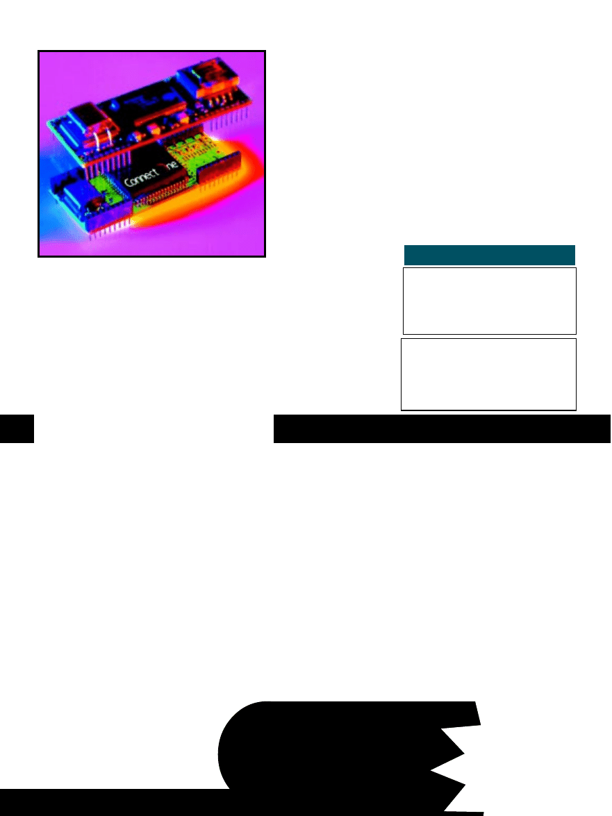
82
Issue 115 February 2000
CIRCUIT CELLAR
®
www.circuitcellar.com
CIRCUIT CELLAR
Test Your EQ
CIRCUIT CELLAR
What’s
your EQ?
—The answers and 4
additional questions and answers are
posted at www.circuitcellar.com.
You may contact the quizmasters
at eq@circuitcellar.com.
8
more EQ
questions
each month in
Circuit Cellar Online
see pg. 2
Tom Cantrell has been working on
chip, board, and systems design and
marketing in Silicon Valley for over a
decade. Reach him by e-mail at
tom.cantrell@circuitcellar.com, by
telephone at (510) 657-0264, or by fax
at (510) 657-5441.
SOURCES
CO560AD-S/P iChip
Connect One Ltd.
972-9-766-0456
Fax: 972-9-766-0461
www.connectone.com
SocketModem
Conexant Systems, Inc.
(800) 854-8099
(949) 483-6996
www.conexant.com
THE MAIL WILL GO
THROUGH
In the future, I-way
connections will find
their way into all kinds of
chips, much as serial
ports (UART, SPI, I
2
C,
etc.) have migrated onto
peripheral ICs, sensors,
and memory chips (e.g.,
serial EEPROM).
That will be fine tomorrow, but
today the race is on to get embedded
apps on the ’Net ASAP. Emerging
solutions like the iChip offer design-
ers a convenient way to add Internet
features to their products without a
lot of up-front expense, risk, and most
importantly, time. Yes, it may not be
as elegant as a bottom-up redesign,
but you can ship tomorrow and do
something whizzier later.
Photo 1
—The embedded iModem
module ($110 in 1k quantities) com-
bines an iChip with a SocketModem
from Conexant for a fully integrated
solution.
to add iChip e-mail capabilities is
literally a plug-and-play proposition,
assuming there’s enough headroom to
accommodate the higher profile
(0.866
²
) of the two-board stack.
Otherwise, pick your favorite mo-
dem module and have at it. If tiny and
tidy packaging isn’t a must, just add
an RS-232 chip and find a deal for a
truckload of fire-sale priced commod-
ity external modems.
Should designers add ’Net features
to embedded applications? Does the
world need a wired vending machine?
The answer from iChip and other
emerging low-cost embedded ’Net
solutions is, now that it can be done,
it will be done.
I
Problem 2
—Why can a flash loader program that receives Intel-hex or Motorola S
records safely discard any record in which every byte to load is a 255?
Problem 3
—Engineer George built a battery-voltage monitor using a 5-V-only
ultra-low-power op-amp as a unity gain buffer and one channel of a four channel
multiplexed A/D on a PIC16C71. Sample time was set to 15 µs. Typical slew rate
(SR) for the op-amp was 0.025 V/µs at 5 V with an output impedance of <500
W
.
Input leakage current for the microprocessor pins was specified at ±1µA max with
leakage to ground increasing by 500 nA during A/D sampling.
The monitor works correctly if the input voltage into the buffer (Vin) is over 2.5 V,
Problem 1
—This function was written to read several values from an A/D converter
and average them together to reduce signal noise. However, subsequent observation
showed no change in the noise characteristics whether sample averaging was used or
not. Can you identify the problem in this code?
unsigned short read_adc(void) {
static unsigned short *p_adc = (unsigned short *)0x8000;
unsigned short i, sum;
sum = 0;
for (i=0; i<10; i++) {
sum+= *p_adc;
}
return (sum/10);
}
but returns low readings for voltages below 2.5 V.
Inspection of the buffer output reveals a –0.5-V pulse 20
µs in duration when the voltage is sampled by the A/D
with no corresponding waveform on the buffer input.
PCB layout ensures little or no noise is entering the
circuit via ground, power supply, or EMI. What is the
problem and solution?
Problem 4
—Johnny implemented a PWM controller in an FPGA as a countdown
timer. The timer is reloaded from a PWM table in memory each time it reaches 0. A
state machine implemented elsewhere in the FPGA determines the reload value. The
equations for the most significant bit of the 6-bit timer are,
tmr_5 = ((tmr_5 & !tmr_load) $$ ((!tmr_load & !tmr_4 & !tmr_3 &
!tmr_2 & !tmr_1 & !tmr_0) # (tmr_load & reload_5)))
tmr_load = (!tmr_5 & !tmr_4 & !tmr_3 & !tmr_2 & !tmr_1 & !tmr_0)
tmr_load
is the reload signal for the timer and is also used as a clock signal to
increment the PWM controller state machine.
Reload_5
is bit 5 of the next value to
be loaded into the timer, determined by the PWM controller state machine.
tmr_5
through
tmr_0
are a set of D registers (clocked by the system clock) that hold the
current count. Operators are: $$ = Boolean XOR, & = Boolean AND, # = Boolean OR.
Johnny was having trouble fitting his design into the FPGA so, to conserve a few
macrocells, he changed the equations to the following,
tmr_5 = (tmr_5 & !tmr_load) $$ ((!tmr_load & !tmr_4 & tmr_a) #
(tmr_load & preload_5))
tmr_load = (!tmr_5 & !tmr_4 & tmr_a)
tmr_a = (!tmr_3 & !tmr_2 & !tmr_1 & !tmr_0)
Equations for bits 0 through 4 were implemented in a similar way using
tmr_a
as
an intermediate value. Johnny found out later that some units in the field worked
properly but some had problems with the state machine advancing through its cycle
too rapidly. What is the source of the problem and what are some possible solutions.
96
Issue 115 February 2000
CIRCUIT CELLAR
®
www.circuitcellar.com
lthough I generally don’t procrastinate forever, that’s exactly what I did when it came to updating my home-
control system. It’s my opinion that when something ain’t broke, it usually will be by the time you get done "fixing" it!
It’s not that my HCS system is so elaborate mind you, it’s just that there are wires going everywhere! Even though I
mentioned fixing it six or seven months ago, it took me two months just to find the wire list.
Another obstacle to “fixing” my system was that it was never a standard configuration. When it comes to HCS II systems, 99% of them
use a single-board controller called a DX board. Direct I/O expansion is accomplished with simple piggyback boards. Network expansion is
done with an RS-485 twisted pair. Everything is quite straightforward.
The bad news is that I emulated the HCS system using a much more expensive variety of industrial-control boards rather than a
standard DX. Because I owned the company that made all the stuff, my cost of ownership was basically zero anyway, so why not? Instead
of a single-board controller with fixed expansion capability, I have an electro-maze wall full of boards, and a hundred direct-wired opto-
isolated inputs and relay outputs (wired to who knows what).
Now that I don’t own the company anymore, converting my custom HCS to a more traditional configuration is traumatic, to say the least.
I wouldn’t care, except that when you’ve lived in an automatic environment for years, it’s a shock to be without it. I didn’t install a 14-kW
diesel generator just so I could work in the Circuit Cellar during a hurricane. I installed a continuous-duty generator because when you live in
an electronic house, it’s either on or off! There’s no middle ground.
I admit that I took the coward’s way out with a dual repair strategy—program accomodation and system surrogates. The latter was
easiest, of course. All this aggravation was about a calendar change, right? What if my HCS never knew it was 2000? Could I squeak a little
more time out of the present configuration? I dusted off an old ’386 running DOS and put it on the filing cabinet next to the HCS. The
machine booted perfectly. It even still had all the HCS software on the hard drive. All I did was load the latest compiled program and attach
the serial cable from the ’386 to the HCS. My control program doesn’t actually care what the calendar date is. I don’t have any parameters
that are day-of-the-month sensitive, and I’d chuck my one weekend-dependent schedule in the interest of accomodation. My HCS chokes if
the PC talking to it tries to download a 2000+ date. Set the ’386 to any date before that and the program loads fine. The HCS may think it’s
1980, but a day in 1980 is the same 24 hours as a day in 2000!
If accomodation failed, I’d have to fix this bucket of transistors real fast (not a pleasant thought). Rather than just ripping things off the
wall, I configured a second HCS system using currently available hardware. I figured if I could string a few critical I/O connections to the
second system, I could at least keep the X-10 modules running should “fixing” the wall ultimately prove fatal to the patient.
I configured a second HCS and paralleled a bunch of direct I/Os from the old system (motion detectors and door switches) to it. I loaded
the automatic lighting section of my program. To make sure I could tell the new code from the old system, I placed X-10 modules (with light
bulbs) in the appropriate rooms. Simple enough to test the new system, just walk in the rooms and the X-10 lights should go on. Simple in
theory. I spent hours inspecting and changing my program. I even hooked a scope up to the X-10 transmitter. The HCS saw the motion
detector and transmitted fine, the signal just wasn’t getting there. The old system was turning the lights on but the new one seemed dead.
The wiring system in our house is an electrician’s nightmare. Every new addition required another breaker panel. Throw in generator
cross-over switches and about five miles of wire in the four buildings and six electrical panels, and it’s a wonder it ever worked. Suspecting
that signal loss had finally gotten too much, I installed active couplers in two of the panels and bought an X-10 signal strength meter. It still
didn’t work. Were the old system’s receivers still loading down the signal? After three days of checking all the variables, I was still stumped.
Finally, I disconnected the X-10 modules from the old system. My wife took a walkie-talkie up to the solarium and sat next to one of the new
modules while I stood next to the HCS in the cellar.
“I just made another program change, Dear. Wave your hands in front of the motion detector and tell me if the light goes on.” Of course,
when you’re married to a crazy inventor you expect to have to do things like this occasionally.
She waved and nothing happened. “Are you sure you sent the signal?”
“I have the laptop sitting here with a PL-Link monitoring the power line and it just said ‘module B4 on’. I know it was transmitted!”
There was a long pause then she answered back, “B4? The switches on the front of this module say A4.”
At that point I knew it was going to be a long Y2K conversion.
“Thanks, Dear. I think we’re done for now.”
PRIORITY
INTERRUPT
steve.ciarcia@circuitcellar.com
You’ve Got to be Y2Kidding
a
Wyszukiwarka
Podobne podstrony:
circuit cellar1995 02
circuit cellar1991 02,03
circuit cellar1994 02
circuit cellar2003 02
circuit cellar2004 02
circuit cellar2002 02
circuit cellar1993 02
circuit cellar1997 02
circuit cellar1990 02,03
circuit cellar2001 02
circuit cellar1996 02
circuit cellar1992 02,03
circuit cellar1992 02,03
circuit cellar1993 02
circuit cellar1991 02,03
circuit cellar1994 02
więcej podobnych podstron