wisdom holds that
embedded applications require special embedded
controllers and interfaces, we’re starting to see that
wisdom challenged. When cost, not size, is the primary
concern, off-the-shelf solutions from the desktop arena often offer a better
price/performance ratio than their semicustom cousins.
A good example is Ed’s embedded ‘386SX series. He’s been able to
show that by using inexpensive, “jelly-bean” motherboards instead of tiny,
specialized controllers, costs stay down without sacrificing performance.
I had occasion in the past few weeks to come across another example,
though with a much smaller market. Caller ID, a service provided by the local
phone companies across the U.S., provides the called
with the caller’s
phone number (and sometimes name) before answering the phone. Caller
ID boxes that display and record the data are available from many
electronics suppliers in a price range of
Most of these units are
stand-alone devices, though. Interfacing them with a computer to make
further use of the information is a costly and
proposition.
Some of these boxes do have a serial port tacked on the side, but it
drives the price up well over $100 for the unit. There is a better alternative.
If you can do without the fancy display (e.g., your application uses a
voice to notify you who’s calling), many modems on the market today offer
Caller ID as an additional feature to the normal data and fax capabilities.
Why pay over $100 for a box that does nothing but Caller ID when you can
get a modem to do the whole deal for under
Another good example of reusing other solutions can be found in one
of our articles this month. Infrared-based printers intended for use with
intelligent calculators are inexpensive and readily available. Using them in
an embedded application is a simple matter of knowing what codes to
send. Why pay triple the price for a special-function, battery-operated printer
when a low-cost, canned solution exists?
Such economies of scale helped put a virtual end to build-your-own
PCs (though no amount of monetary savings could match the pleasure many
of our readers derive from making their own). This trend is now moving into
the embedded peripheral market where A/D converter boards, Caller ID
boxes, and tiny printers have so many features included that it doesn’t make
sense to roil your own. The functional& is already there! And who has the
time or money, anyway?
There will always be a place for custom and semicustom solutions,
especially with constraints on size, weight, power usage, and so forth. Such
engineering is our lifeblood. We just have to be sure to keep an open mind
when design specs aren’t tight.
CIRCUIT
T H E C O M P U T E R A P P L I C A T I O N S J O U R N A L
DIRECTOR
PUBLISHER
Steve Ciarcia
Daniel Rodrigues
EDITOR-IN-CHIEF
PUBLISHER’S ASSISTANT
Ken Davidson
Sue Hodge
TECHNICAL EDITOR
CIRCULATION COORDINATOR
Janice Marinelli
Rose
ENGINEERING STAFF
CIRCULATION ASSISTANT
Jeff Bachiochi Ed Nisley
Barbara
WEST COAST EDITOR
CIRCULATION CONSULTANT
Tom Cantrell
Gregory Spitzfaden
CONTRIBUTING EDITOR
BUSINESS MANAGER
John Dybowski
Jeannette Walters
NEW PRODUCTS EDITOR
ADVERTISING COORDINATOR
Weiner
Dan Gorsky
ART DIRECTOR
CIRCUIT CELLAR INK, THE COMPUTER
Lisa Ferry
JOURNAL
published
monthly by Circuit Cellar Incorporated. 4 Park Street.
GRAPHIC ARTIST
20, Vernon, CT 06066 (203) 675.2751. Second
Joseph Quinlan
One-year issues)
rate U.S.A. and
PRODUCTION STAFF
John Gorsky
$49.95. All
orders payable
I
” U.S.
James Soussounis
funds only,
postal money order
check drawn on U.S. bank.
orders
CONTRIBUTORS:
and
related
Cellar INK
Jon Elson
P.O. Box 696, Holmes. PA 19043.9613
Tim
call
269-6301.
Frank Kuechmann
POSTMASTER, Please send address changes to
Kaskinen
P.O.
Holmes,
PA
Cover photography by Barbara Swenson
PRINTED IN THE UNITED STATES
ASSOCIATES
NATIONAL ADVERTISING REPRESENTATIVES
NORTHEAST
MID-ATLANTIC
Barbara Best
(908) 741-7744
Fax: (908)
SOUTHEAST
Collins
(305) 966-3939
Fax: (305) 985-8457
MIDWEST
Nanette Traetow
(708)
Fax: (708) 789-3082
WEST COAST
Barbara Jones
Shelley Rainey
(714) 540-3554
Fax: (714) 540-7103
300112001240019600114 4k bps.6
1
24001
9600 bps Courier HST, (203)
All programs and schematics
been carefully
to
transfer by subscribers
any
these
programs schematics for the consequences any such
Furthermore. because of possible
the
and condition of materials and workmanship of reader-assembled projects,
INK
disclaims any
the safe and proper
of reader-assembled projects based upon from
plans,
published in Circuit Cellar INK.
contents
1995 by
Cellar Incorporated All rights reserved.
of
public&on whole in
consent from
Cellar Inc.
2
Issue
February 1995
Circuit Cellar INK

1 4
1 8
2 2
3 0
3 6
5 0
6 0
6 8
7 6
Interfacing Flow Meters to High-speed Counters
by Bill Payne
Use Infrared to Make Embedded Printing Easy
by
Fisher
It’s Not Just for Memory Anymore
An Introduction to PCMCIA
by Lalo Gastriani
Speeding and Slimming Your Port Access
A Different Way of Reading from the PC Parallel Port
by
Lee Kok-Leong Ong
Battery-operated Power Supplies
Selecting the Right Battery and Supply for Your Application
by David
q
Firmware Furnace
Journey to the Protected Land: Infrastructure Improvement
Ed Nisley
q
From the Bench
Fitting 10 oz. into a
Package
An Application for Highway Safety
Bachiochi
q
Silicon Update
I Sync, Therefore I DRAM
Tom Can
Letters to the Editor
New Product News
q
Embedded Techniques
Downsizing
1
Flash-based Microcontroller
Dybowski
edited by Harv Weiner
Circuit Cellar INK
Issue
February 1995
NEW COVER-A STEP UP
I got the latest INK today-very professional
looking. It reminds me of
Science
or such. Of
course, the contents are much better than those other
magazines!
Hope y’all have a great ‘95
Russ
CT
PRAISE AND FIXES
I really enjoy Ed Nisley’s series on protected-mode
programming. At the moment, my only application is
writing assembly language subprograms to run under
Lahey FORTRAN
which runs under the
Pharlap DOS extender. Even so, I’ve found several
helpful nuggets of information. If Ed wants to explain
how to write an interrupt service routine for IRQ2
(vertical retrace) running in protected mode under
Pharlap, I wouldn’t mind at all.
As an ancient controls engineer (MIT
I noticed
that Tom Cantrell’s PID-pong control loop has the
gains set wrong. The response shown in Figure 5 (INK
50)
is much too oscillatory. You can see, not quite
hidden by the noise, a slowly decaying sine wave in the
fan plot starting after each change in the position
setpoint.
The frequency of the sine wave is the natural
frequency of the entire system; it shouldn’t be so
prominent in the responses. In a well-designed system,
it would damp out in a couple of cycles or less after a
change in setpoint. With this design, the motor has to
work too hard and there is little stability margin. A few
decibels gain increase (temperature or whatever) could
make the design unstable.
To improve the response, set the gain to zero. Try
reducing the gain or increasing the D gain. Up to a
point, increasing the D gain allows for higher values of
the gain without making the response too oscillatory.
Once you get good values for the and D gains,
increase the I gain as far as possible without spoiling
the transient response. Small test inputs should be used
in this stage. Finally, adjust the nonlinear parameters
for the largest inputs you expect.
James C. Wilcox
Palos Verdes Estates CA
P.S.: Thanks for sending a replacement for the issue
that the postal service mangled.
Editor’s Note: The March issue features fuzzy logic and
will be offering two fuzzy-pong designs. Be sure to pick
up a copy so you can compare Tom’s technique with a
fuzzy approach.
FOR YOUR INFORMATION
Thank you for featuring
Microchip
Technology
new fuzzy logic development tool, in
your December ‘94 issue. Several readers have asked us
how to obtain more information about Inform Software
Corporation, Evanston, Ill., who developed the fuzzy
logic tool suites for this device. Inform Software can be
reached at (800) 929-28 15. The
product
is available only through any Microchip worldwide sales
office and authorized dealer or by calling (602) 786-7668.
Eric Sells
Public Relations Manager
Microchip Technology, Inc.
Contacting Circuit Cellar
We at Circuit Cellar
communication between
our readers and our staff, so have made every effort to make
contacting us easy. We prefer electronic communications, but
feel free to use any of the following:
Mail: Letters to the Editor may be sent to: Editor, Circuit Cellar INK,
4 Park St., Vernon, CT 06066.
Phone: Direct all subscription inquiries to (800)
Contact our editorial offices at (203) 875-2199.
Fax: All faxes may be sent to (203)
BBS: All of our editors and regular authors frequent the Circuit
Cellar BBS and are available to answer questions. Call
(203) 871-1988 with your modem
bps,
Internet: Electronic mail may also be sent to our editors and
regular authors via the Internet. To determine a particular
person’s Internet address, use their name as it appears in
the masthead or by-line, insert a period between their first
and last names, and append
to the end.
For example, to send Internet E-mail to Jeff Bachiochi,
address it to
For more
information, send E-mail to
6
Issue
February 1995
Circuit Cellar INK
Edited by Harv Weiner
MINIATURE CCD CAMERA
A miniature breadboard-type CCD black white camera
(1.26” x 1.26”
x 0.75”)
is available from Edmund Scientific. The camera can be used for
home and office security, robotics, machine vision, and instrumentation
applications.
The unit produces video output with an automatic electronic shutter
and features a 3.7-mm pinhole lens built into the breadboard assembly. The
field of view is 45” vertical x 60” horizontal with 32-mm x 32-mm dimen-
sions. Miniature details can be observed on a TV monitor from a range of
only inches up to 15’ with a
minimum illumination. Resolution is
380 TV lines horizontal by 350 lines vertical. The unit uses
input.
Edmund Scientific Co.
Dept.
Edscorp Bldg.
l
Barrington, NJ 08007
(609) 573-6259
l
Fax: (609) 573-6295
EMBEDDED SYSTEM DEVELOPMENT TOOLS
Lap’s new TNT Embedded
delivers a total solution for
embedded-systems development on
the Intel
family of microprocessors. The suite offers an easy and cost-effective, one-stop solution for building
embedded applications using popular DOS and Windows compilers. Supported compilers include
C/C++
products from Borland, Microsoft, and
The
components include the TNT Embedded Kernel, Visual System Builder, LinkLoc (a
linker
and locator), and CVEMB and TDEMB shells for embedded cross-debugging. Full support for C/C++ run-time librar-
ies, an MS-DOS-compatible file system, and a floating-point-emulation library are also included.
The TNT Embedded Kernel provides a simple operating system for running embedded programs. Its two main
functions are to initialize
protected mode and provide the foundation for running a C/C++ run-time library.
These functions can save development time since developers don’t have to set up their own protected-mode environ-
ment or learn new run-time libraries. The Kernel can be loaded from ROM or diskette. The Kernel also includes a
floating-point emulator, native MS-DOS file system, and a remote file system.
The Visual System Builder enables developers to configure and customize the TNT Kernel to match their
hardware setup through an easy-to-use Windows utility. Developers can specify where memory is located in the
target, how the kernel is loaded into memory, and how the target system communicates with the debugger.
As a sophisticated one-step linker/locator,
LinkLoc builds embedded applications that run
on the TNT Embedded Kernel. LinkLoc includes
a rich set of command switches to control the
entire link process. It can provide full symbolic
information for C/C++ source-level debugging
with
or Turbo Debugger. In addition,
it can output files for an in-circuit emulator or
PROM programmer.
The TNT Embedded
sells for
$2995. Requirements include a PC-compatible
host computer running DOS and Windows 3.1.
Phar Lap Software, Inc.
60 Aberdeen Ave.
l
Cambridge, MA 02138
(617) 661-l 510
l
Fax: (617) 876-2972
Issue
February 1995
Circuit Cellar INK
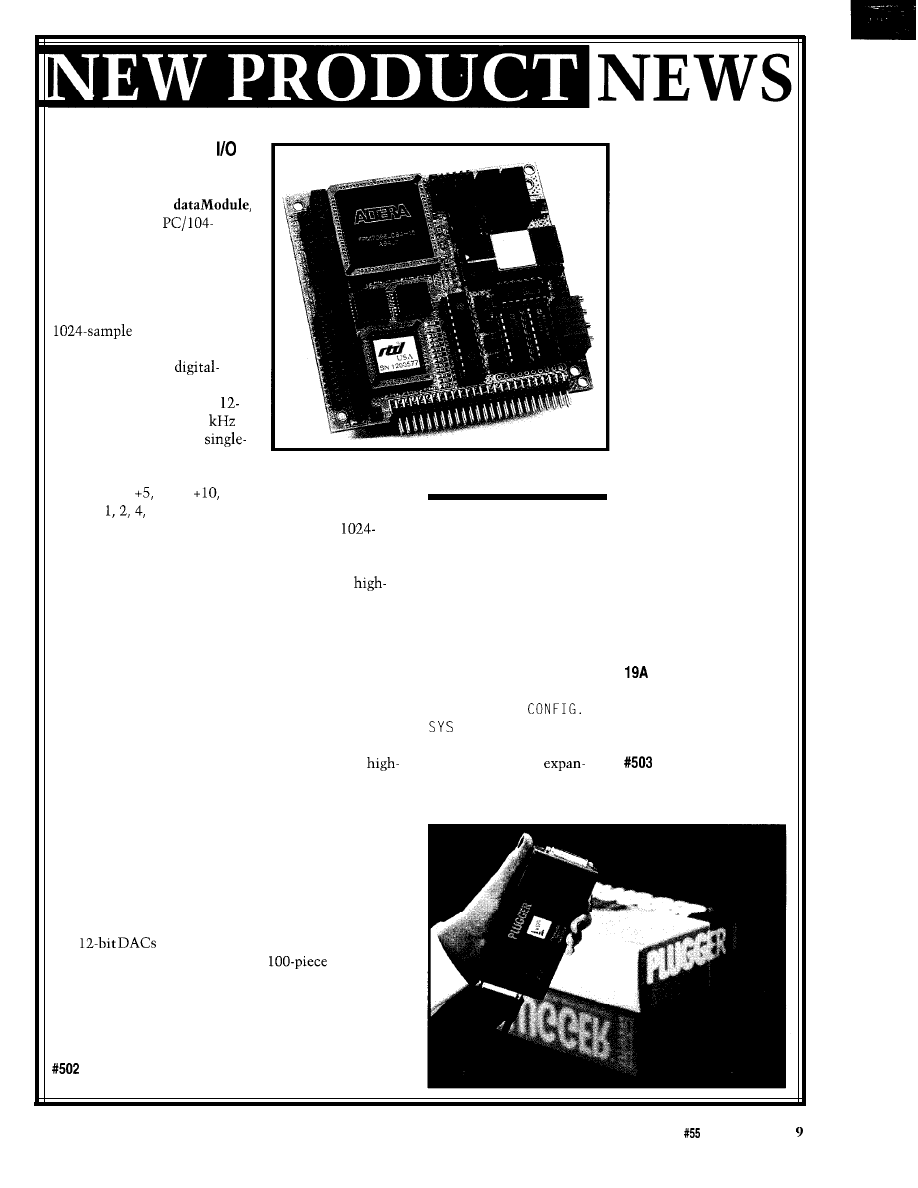
HIGH-SPEED ANALOG
MODULE
Real Time Devices intro-
duces the DM5408
an ultracompact,
compliant data acquisition and
control module for OEM
embedded and portable applica-
tions. The DM5408 features
channel-gain scan memory,
A/D buffer, and
bit-programmable digital I/O
with two advanced
interrupt modules.
The DM5408 features
bit A/D converter at 200
with 8 differential or 16
ended channels. Inputs are
jumper configurable for three
ranges: -5 to
-10 to
or 0 to 10 V. Programmable
gains of
and 8 can be combined with the input
ranges to optimize gain/resolution tradeoff. A
sample buffer provides an interface between the A/D
PARALLEL PORT
converter and PC to enhance triggering and storage
HARD DRIVE
capabilities and to maintain data integrity. Four
Computer Connections
speed, digital-input lines, synchronized to the conversion
America has introduced
rate and stored in the buffer, can be used as a 4-bit data
Plugger,
a
2.5”
hard drive
or trigger marker without interrupting conversion.
that installs on any parallel
The channel-gain scan memory offers channel
printer port. Plugger does
sampling in any order with a different gain on each
not require additional
channel at high speeds. A skip bit is included to support
hardware for DOS and OS/2
different sampling rates on different channels, thereby
systemsandno
saving memory and eliminating the need to discard
changes are needed.
unwanted data. Digital output lines are also provided to
Plugger is an ideal solution
control TMX32 analog-input expansion boards for
for mobile storage
speed scanning of up to 5 12 random channels. The
sion, file transfer, backups,
DM5408 has several triggering and conversion modes
and PC installations.
supported through the hardware and software including
pre-, post-, and about-trigger, channel scanning, and
random- and multiburst.
The bit-programmable digital I/O lines support two
advanced digital-interrupt modes. An interrupt can be
generated when the lines match a programmed value or
when any bit changes its current state. There are also
two
and two 16-bit timer counters.
The DM5408 sells for $450 in
quantities.
Real Time Devices, Inc.
P.O. Box 906
l
200 Innovation Blvd.
State College, PA 16804
l
(814) 234-8087
l
Fax: (814) 234-5218
Capacities range
from 170 to 810 MB and
access time is 12 ms.
The unit weighs only 11
oz. and is less than 1” x
3” x 6” in size. Pluggers
are EPP compliant and
pass printer information
through untouched. The
Plugger ships as a
complete kit, which
includes a carrying case,
DOS and OS/2 drivers,
keyboard and mouse
power adapters, AC wall
plug, and installation
guide. No controller card
is needed. Pluggers
support Stacker and
Double Space which
increases capacity to well
over 1 GB.
Plugger list prices
range from $499 to $999
and have a two-year
warranty.
Computer Connections
America
Crosby Dr.
Bedford, MA 01730
(617) 271-0444
Fax: (617) 271-0873
Circuit Cellar INK
Issue
February 1995
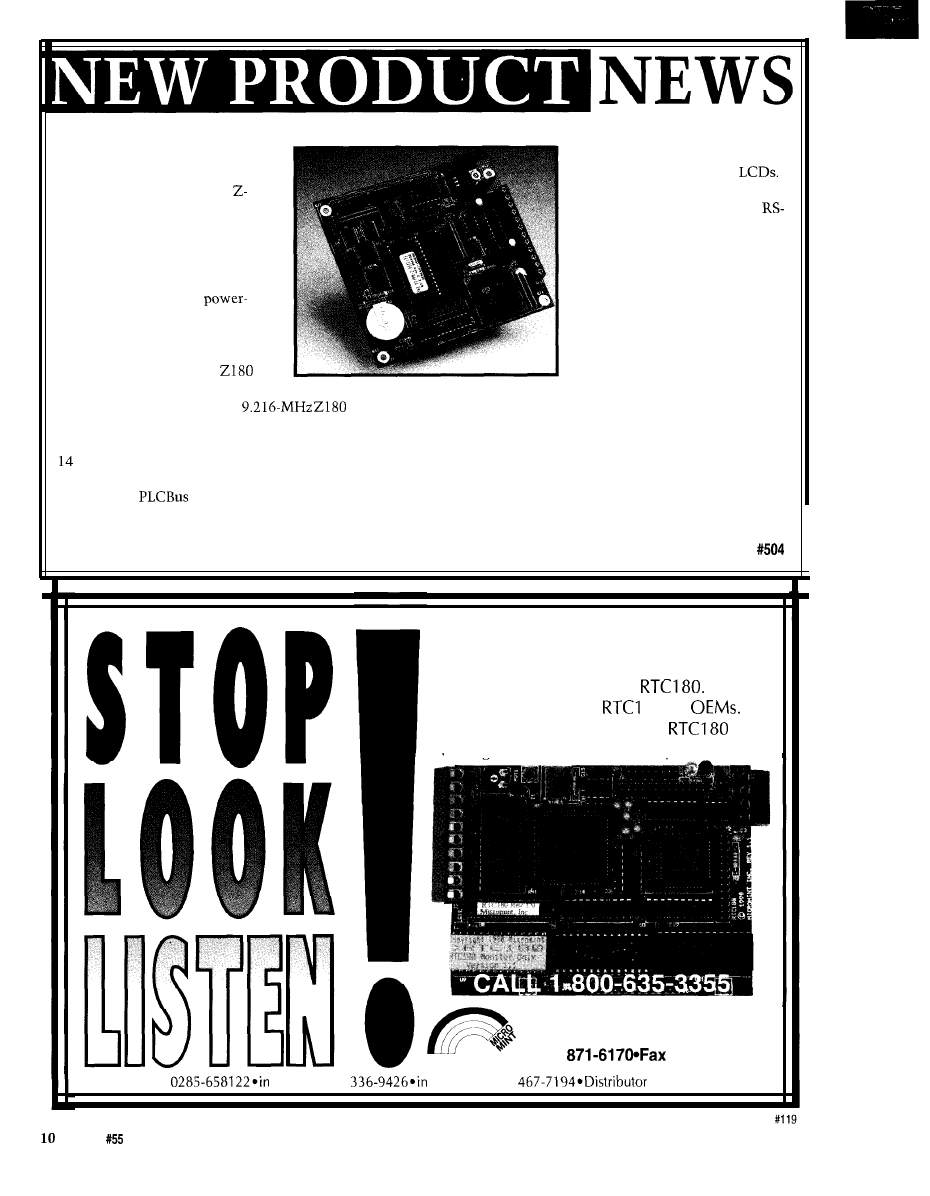
C-PROGRAMMABLE
CONTROLLER
The
Little Genius from
World is a compact, low-cost con-
troller appropriate for control and
data-acquisition applications.
Standard features include a battery
backup for RAM and real-time
clock, watchdog timer,
failure interrupt, EEPROM for
system constants, up to 5 12 KB
RAM and up to 512 KB EPROM
(32 KB standard), and two
DMA channels.
The Little Genius uses a
micro-
controller and is packaged on a 4.5” x 4.2” board. Fully
populated, the Little Genius provides 12 digital inputs,
digital outputs, serial communication, programmable
timers, back-up battery, and large memory space. A con-
nector to the
provides room for expansion
boards; a piggyback prototyping board is being developed.
solenoid actuators, solid-state
relays, and many kinds of
There are two asynchronous ports
that can be configured as two
232 channels or one RS-232 and
one RS-485 channel. The ports
operate up to 57.6 kbps.
The Little Genius is sup-
ported by Z-World’s Dynamic C
development system which com-
bines a text editor, fast compiler,
and symbolic debugger. Dynamic
C comes with dozens of function
libraries (including a real-time
kernel] and sample programs in source code. It is avail-
able for DOS and Windows.
The Little Genius sells for $149 and includes a sche-
matic, manual, and wall transformer. Other configura-
tions and options are available.
Z-World Engineering
The unit has been designed to accommodate key-
1724 Picasso Ave.
l
Davis, CA 95616
pads or arrays of contacts of up to 84 elements, relays,
(916) 757-3737
l
Fax: (916) 753-5141
Odds are that some time during the day you
will stop for a traffic signal, look at a message
display or listen to a recorded announcement
controlled by a Micromint
We’ve
shipped thousands of
80s to
Check out why they chose the
by
calling us for a data sheet and price list now.
MICROMINT, INC.
4
Park Street, Vernon, CT 06066
(203)
(203) 872-2204
in Europe: (44)
Canada: (514)
Australia: (3)
Inquiries
Welcome
Issue
February 1995
Circuit Cellar INK
NEWS
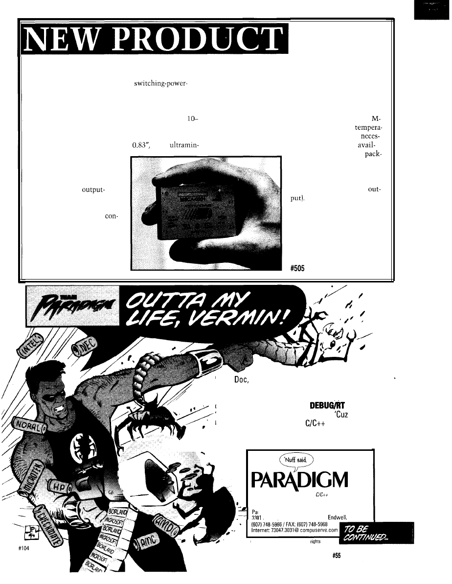
ULTRAMINIATURE SWITCHING POWER SUPPLY
The M-Series of AC/DC switching modules provide
Designed to meet the compact
input-to-output isolation of 3750 VAC and are available
supply requirements of portable systems, embedded
in both commercial and low-leakage UL-544 medical
controls, and medical equipment, the M-Series AC/DC
versions. The modules meet UL, CSA, and TUV safety
switching power-supply modules
from Astrodyne accept
and FCC and VDE Level B EM1 requirements. They also
universal input over the ranges of 85-265 VAC and
1
include output-overvoltage protection circuitry. The
340 VDC as well as providing single, dual, and triple
Series power supplies operate over the ambient
outputs in voltage ranges of 3.3-24 VDC.
ture range of 0-50°C without the output derating
Measuring just 2.55” x
1.77” x
these
sary when using convection cooling. Models are
iature modules provide power
able in a wide variety of
densities of up to 2.8 W per
aging and interconnection
cubic inch and include unique
styles.
features such as an integral
M-Series power supply
potentiometer for
prices start at $59 (single
voltage adjustment and an
LED power-status indicator.
Remote power on and off
Astrodyne
trol is provided via a single
412 High Plain St.
logic-level control pin, making
Walpole, MA 02081
the M-Series ideal for use in
(508) 668-2311
energy-saving designs in which
Fax: (508) 668-9942
auto shutdown of power is
desirable.
If, like
you think bugs belong six feet under, then step
up to
Paradigm DEBUG
and get the right weapon for the
toughest
‘186
or V-series embedded application. Take ‘em
on by yourself with
Paradigm
or gang up on
em with a popular in-circuit emulator.
no matter what
kind of Borland or Microsoft
vermin you’re fightin’,
ya better not go in empty-handed or firing blanks from
inferior weapons. Ya just might not live to regret it.
Proven Solutions for Embedded
Developers
I-800-537-5043
radigm Systems
Country Club Road, Suite 2214,
NY 13760
01994 Paradigm Systems. Inc. All
reserved.
Circuit Cellar INK
Issue
February 1995
11
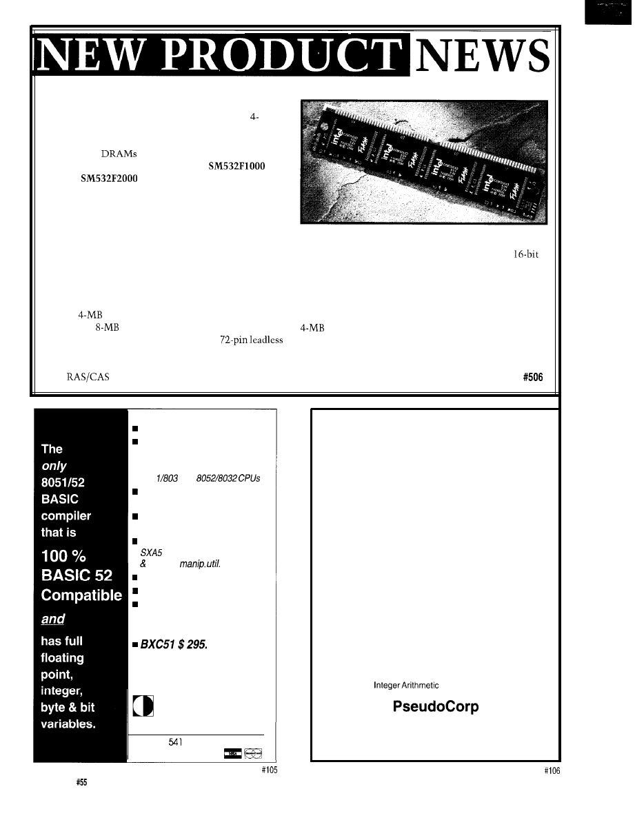
FLASH-MEMORY MODULES
Smart Modular Technologies has developed and 8
MB SIMMs using Intel’s new embedded flash-RAM
integrated circuits which combine the high-speed
readability of
with the nonvolatile update
capabilities of flash. Designated as the
(4
MB) and
(8
MB), the new CMOS flash
modules are targeted at high-performance embedded
applications which previously stored programs or
executable files in ROM or on disk and downloaded
them into volatile DRAM for operation.
The flash-RAM modules are ideal for storing
instantly executable programs such as BIOS, DOS and
other operating systems, Windows application packages,
fonts for printers, and other executable code. The
modules thus save space on a system’s hard drive while
offering instant-on operation.
The
module is organized as 1 megaword by 32
bits, and the
module is organized as 2 megawords
by 32 bits. Both modules are packaged in
SIMMs. Control signals are also DRAM standard. The
SIMMs incorporate a DRAM interface, which accommo-
dates
signals and multiplexed address lines.
The SIMMs are therefore capable of working with
existing DRAM controllers. Control lines permit
word control.
Because the flash-RAM chips are nonvolatile, no
refresh cycles are needed to retain data, a factor that
further lowers CPU overhead and saves power.
Pricing of the new flash-RAM SIMM is $149.85 for
and $279.65 for 8-MB (in quantity).
Smart Modular Technologies, Inc.
45531 Northport Loop West
l
Fremont, CA 94538
(510) 623-l 231
l
Fax: (510) 623-l 434
Memory mapped variables
In-line assembly language
option
n
Compile time switch to select
805
1 or
Compatible with any RAM
or ROM memory mapping
Runs up to 50 times faster than
the MCS BASIC-52 interpreter.
Includes Binary Technology’s
1 cross-assembler
hex file
Extensive documentation
Tutorial included
Runs on IBM-PC/XT or
compa tibile
n
Compatible with all 8051 variants
508-369-9556
FAX 508-369-9549
Binary Technology, Inc.
P.O. Box
l
Carlisle, MA 01741
Cross Assemblers
l
Local Labels and Cross Reference
l
Powerful Macro Substitution Capability
l
Machine Cycle Counting
l
32 Significant Character Labels and Symbols
l
Unlimited Include File Capability
l
Selectable Intel Hex or Motorola Hex Object File
Simulators
l
Source View Symbolic Debugging
l
Attach Keyboard, Screen or Data Files to Simulate I/O
l
Machine Cycle Counting
l
Ten User-definable Screens
l
Unlimited Breakpoints, Memory and I/O Mapping
l
Trace File to Record Simulator Session
l
Ability to Step Backward through Simulation
Disassemblers
l
Automatic Substitution of Defined Label Names for All Jumps
and Branches
*Automatic Insertion of Supplied Comments and Expressions
Application Source Libraries
l
16 and 32 bit
and Numeric/String Conversion
921 Country Club Road, Suite 200
l
Eugene, OR 97401
(503) 683-9173
Fax: (503) 683-9186
BBS (503) 683-9076
12
Issue
February 1995
Circuit Cellar INK
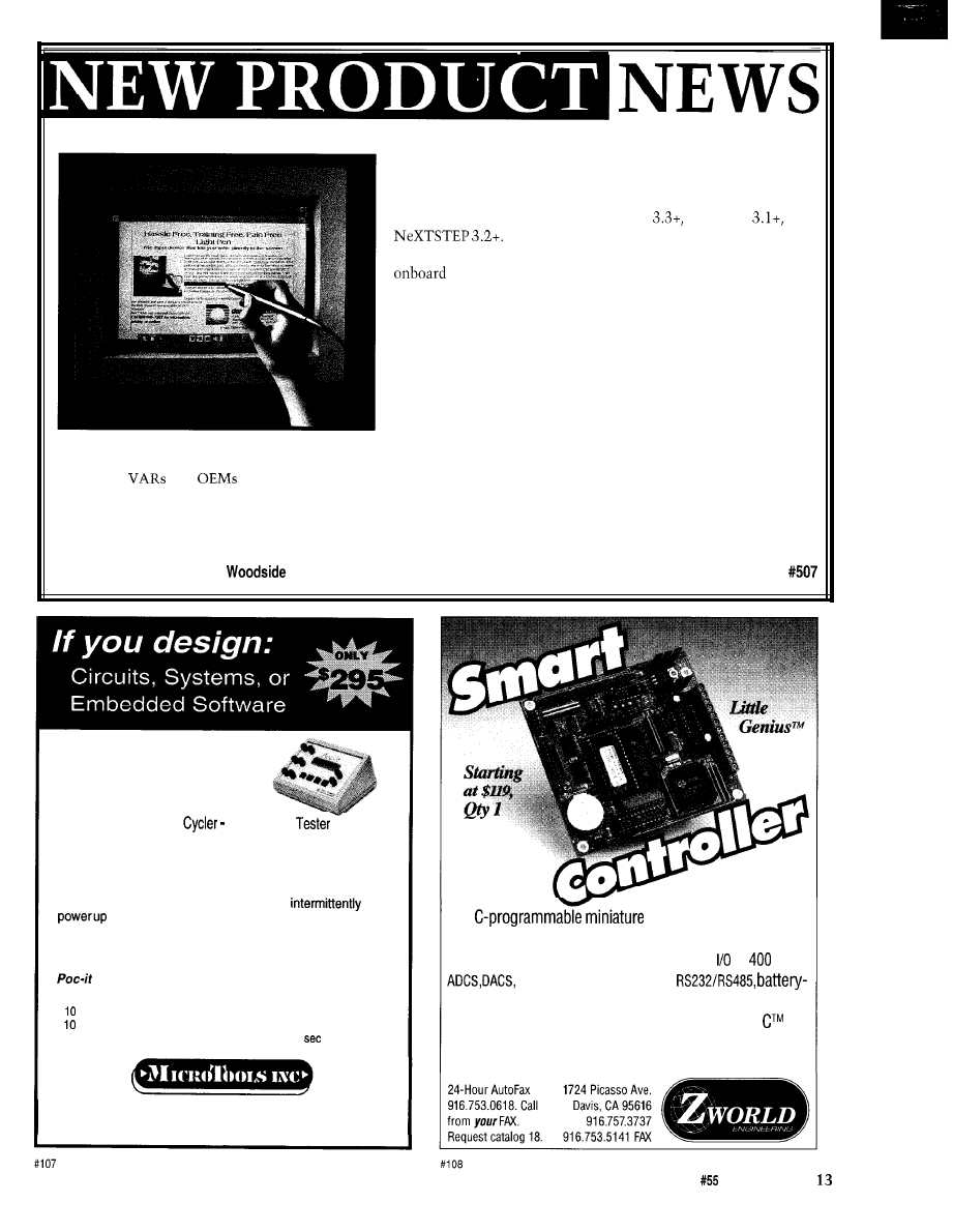
JITTER-FREE LIGHT-PEN INTERFACE
Design Technology has introduced a unique light-pen
interface board. The all-digital DT360 offers fast, smooth opera-
tion. The light pen is available for DOS
Windows
or
The DT360 is a complete system on a board and features an
processor and clock crystal. With much less reference to
the CPU, the DT360 is faster, more accurate, and has much
smoother cursor moves. Because the jitter has been designed out,
there is no lag normally associated with the smoothing process.
In some modes, the smoothness is visibly superior to the mouse
cursor.
The DT360 features locking-function options that prevent
the installation of any other pen or board in the system. The
DT360 can send and receive codes so that if an unauthorized
replacement pen is plugged in, it simply won’t work. Similarly, if
the proprietary software sends a code when an unauthorized interface board has been installed, it won’t work either.
This gives
and
better control of what gets installed in their systems.
The DT360 interface accepts all Design Technology styles of light pen from the basic black anodized aluminum
to a double side-switch, stainless-steel model.
Evaluation systems start at $188 with a money-back guarantee.
Design Technology
l
11489
Ave.
l
Santee, CA 92071-4724
l
(619) 448-2888
l
Fax: (619) 448-3044
Then you need:
Poc-it
Power-On
Intermittent
The circuits, boards, and systems we design today are complex.
We are using more complex components to create these
designs. Thus, we must test these components over a wide
range of scenarios. For example, we have found VLSI chips,
software libraries and hardware designs that
fail to
properly. Tominimizecostly re-workandembarrassing
failures, we must test these designs across a large number and
wide variety of power-up scenarios. Will your design power up
every time?
is designed specifically to help you test your design
for just these scenarios. Featuring:
l
amp
120 VAC receptacle
l
One IO-30VDC sense input
l
amp relay
l
Outputs easily programmable
l
Two 5 VDC high speed inputs
from 0.01
to 100 min.
714
Hopmeadow St., P.O. Box 624, Simsbury, CT 06070
(800)
651-6170
FAX: (203) 651-0019
Our
controllers are
ideal as the
brains for control applications, data acquisition, and test
and measurement. Features include digital to lines,
relays, solenoid drivers,
backed
RAM
,
clock, watchdog,
LCDS
,
keypads, enclosures
and more.
Use
our simple, yet powerful, Dynamic de-
velopment system ($195 integrated editor, compiler and
debugger) for quick project completion!
Circuit Cellar INK
Issue
February 1995
FEATURES
Interfacing Flow Meters to
High-speed Counters
Use Infrared to Make
Embedded Printing Easy
It’s Not Just for Memory
Anymore
Speeding and Slimming
Your Port Access
Battery-operated
Power Supplies
Interfacing
Flow Meters
to
speed
Counters
Bill Payne
amount of fluid
dispensed in a customer
application. The project involved
interfacing a high-speed digital counter
on an embedded controller with a
electromechanical flow meter, an
application commonly found in
beverage, medication, and fuel dispens-
ing systems. You find some type of
flow meter anywhere fluid flow must
be measured. The problems, however,
start when mixing the analog signals
from the flow meters with high-speed
digital systems.
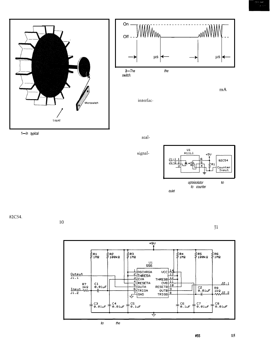
Figure 1 depicts a basic flow
meter. It consists of a paddle wheel
attached to a cam which opens and
closes a switch as it rotates. By placing
the paddle wheel into the fluid flow, a
pulse rate is produced which is
proportional to the flow rate.
Electromechanical flow meters
can be purchased in two basic models.
The newer versions use a rotating
magnet and a Hall-effect transducer.
These are straightforward since the
switch element is a semiconductor
device. The more common type of
flow meter uses a rotating magnet and
a magnetic reed switch. Figure 2
depicts the waveforms at the opening
and closing of the reed switch. As
shown, the reed switches are bouncy
on both opening and closing.
The majority of flow meter
applications do not operate at a high
rate of speed. As an example, the flow
meters in a gasoline dispenser only
provide ten pulses per gallon. Just
think of how long (in microprocessor
cycles) it takes to pump a gallon of gas
into your vehicle’s gas tank.
14
February 1995
Circuit Cellar INK
Paddle wheel
flow
Cam
Figure
a
fluid-flow measuring system, a reed switch is closed on
each
revolution of the paddle wheel.
Unfortunately, most semiconduc-
tor systems do not care about such
low-speed environments. Instead, they
count every bounce of the magnetic
reed switch as a pulse transition.
When you realize that the reed switch
may open and close more than one
hundred times and your flow rate is
only ten pulses per gallon, the problem
becomes obvious.
Open
bounce
75
Close
bounce
75
Figure
jagged pattern marks opening and closing contact bounce for a magnetic
reed
is fine for high-speed
one timing resistor and one capacitor.
communications
It can sink or source up to 200
of
systems, but it is not a
current from or to an output device,
virtue when
which is more than enough current to
ing with slow-speed
drive the LED in an optoisolator. It can
devices such as flow
operate over a 5-15-V range. And most
meters.
importantly, the internal timing
The design in
operation is fairly insensitive to power
Figure 3 has several
fluctuations. This enables the device
limitations in an
to be used in environments that don’t
interface with
have much filtering on the supply.
world analog systems.
There are two different environments
to consider when designing
conditioning circuits for high-speed
counters: one which has fairly clean
signal and power leads and the other
which has AC waveforms capacitively
coupled to the signal and power leads.
Figure 3-A simple
can be
used
DC ENVIRONMENT
interface a flow meter a
in a
relatively slow
and
environment.
The signal conditioning necessary
Figure 3 depicts a common
in a DC environment is usually related
The circuit in Figure 4 can be used
interface to a high-speed counter. The
to the bounce of the magnetic reed
to clean up the output from the reed
digital counter is a standard Intel
switch. One technique used quite
switch in the flow meter. This circuit
This device has a maximum
effectively debounces the reed switch
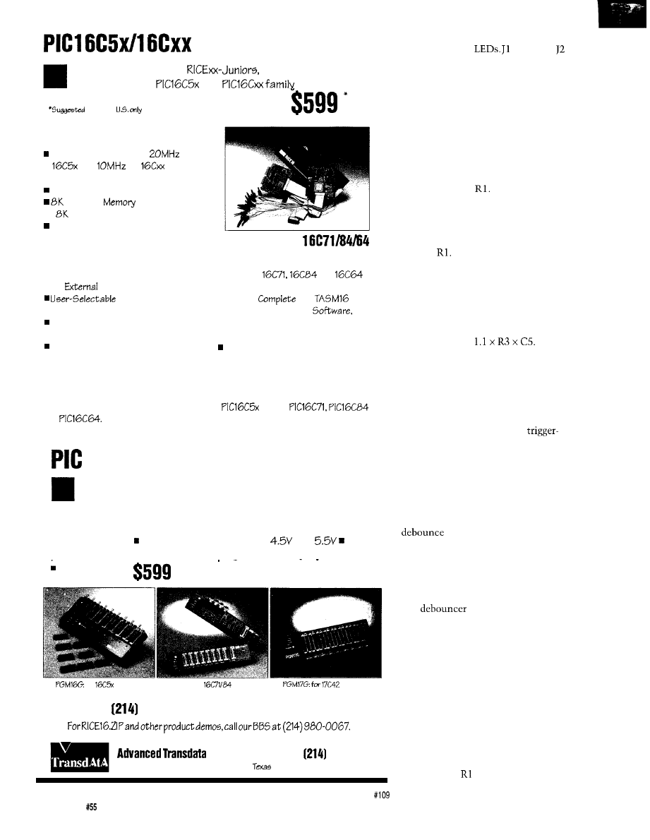
uses a dual 555 timer IC referred to as
counter-input frequency of MHz.
with a 555 timer IC.
a 556 IC. Both timer circuits in the 556
The counter is connected to the
This device can be set to virtually
IC are configured the same. pin 1
outside world through an optoisolator.
any time span through the selection of
and J2 pin 1 are the outputs that drive
In my opinion, this is a
requirement when
working with any control
system. The optoisolator
provides a separation
between the noisy analog
(real world) system and
the digital system.
D S C H R G B
The opto also pro-
vides security for the
digital system in the event
of a catastrophic failure
on the analog side. Some
of the newer optoisolators
have internal Schmitt
triggers to increase their
frequency response. This
Figure 4-A 556 can be used clean up raw flow-mefer signals and generate clean, square pulses.
Circuit Cellar INK Issue
February 1995
Real-time Emulators
Introducing RICE16 and
real-time in-circuit
emulators for the
and
microcontrollers:
affordable, feature-filled development systems from
Retail for
RICE16 Features:
Real-time Emulation to
for
and
for
n
PC-Hosted via Parallel Port
Support; all oscillator type5
Program
n
by 24-bit real-time Trace Buffer
Source Level Debugging
n
Unlimited Breakpoints
n
External Trigger Break with either
“AND/OR” with Breakpoints
n
Trigger
Outputs on any
Address Range
n
12
Logic Probes
Internal
Clock from
40 frequencies or External Clock
Single Step, Multiple Step, To Cursor,
Step over Call, Return to Caller, etc.
On-line Assembler for patch instruction
n
Easy-to-use windowed software
Emulators for
available now!
n
Support
and
with
Optional Probe Cards
n
Comes
with
Macro
Assembler, Emulation
Power
Adapter, Parallel Adapter Cable and
User’s Guide
30-day Money Back Guarantee
n
Made in the U.5.A.
RICE-xx Junior series
RICE-xx “Junior” series emulators support
family,
or
They offer the same real-time features of RICE16 with the
respective probe cards less real-time trace capture. Price starts at $599.
Gang Programmers
Advanced Transdata Corp. also offers PRODUCTION QUALITY
gang programmers for the different PIC microcontrollers.
n
Stand-alone COPY mode from a master device
n
PC-hosted mode
for single unit programming
n
High throughput
n
Checksum verification
on master device Code protection
n
Verify at
and
Each
program cycle includes blank check, program and verify eight devices
Prices start at
for
family
PGM47: for
Call
980-2960 today for our new catalog.
Corporation
Tel
9802960
14330
Midway bad, Suite 120. Dallas.
75244
Fax (214) 980-2937
the optoisolator
pin 2 and
pin 2 are connected to the reed
switches within the flow meters. This
circuit can operate over a 5-15-V DC
range. Using 12 V increases the noise
immunity for the reed switch over
long distances.
CIRCUIT OPERATION
Prior to the closure of the reed
switch, capacitor C3 is charged to 12 V
through resistor
The closing of the
reed switch rapidly discharges capaci-
tor C3 through resistor R7. All bounce
from the reed switch is removed by the
integrating action of capacitor C3 and
resistor
This clean, negative-going spike is
then fed into the trigger input of the
555 timer through capacitor Cl. This
trigger pulse fires the 555 timer
generating an output pulse of
Time=
This output pulse then drives the LED
within the optoisolator. On release of
the reed switch, capacitor C3 recharges
to 12 V and the circuit waits for the
next switch closure.
The time constants and
input filtering send a single pulse for
each closure of the reed switch. With
this design, the circuit does not
retrigger when the reed switch is held
in the closed position. Instead, it
outputs a single pulse and waits for the
next trigger pulse. You can tune the
period by simply altering the
values of the timing resistor and
capacitor.
AC ENVIRONMENT
The circuit in Figure 4 works fine
as a
for the magnetic reed
switch in a low-noise environment.
When put into an environment such as
Figure 5, the circuit can fail miserably.
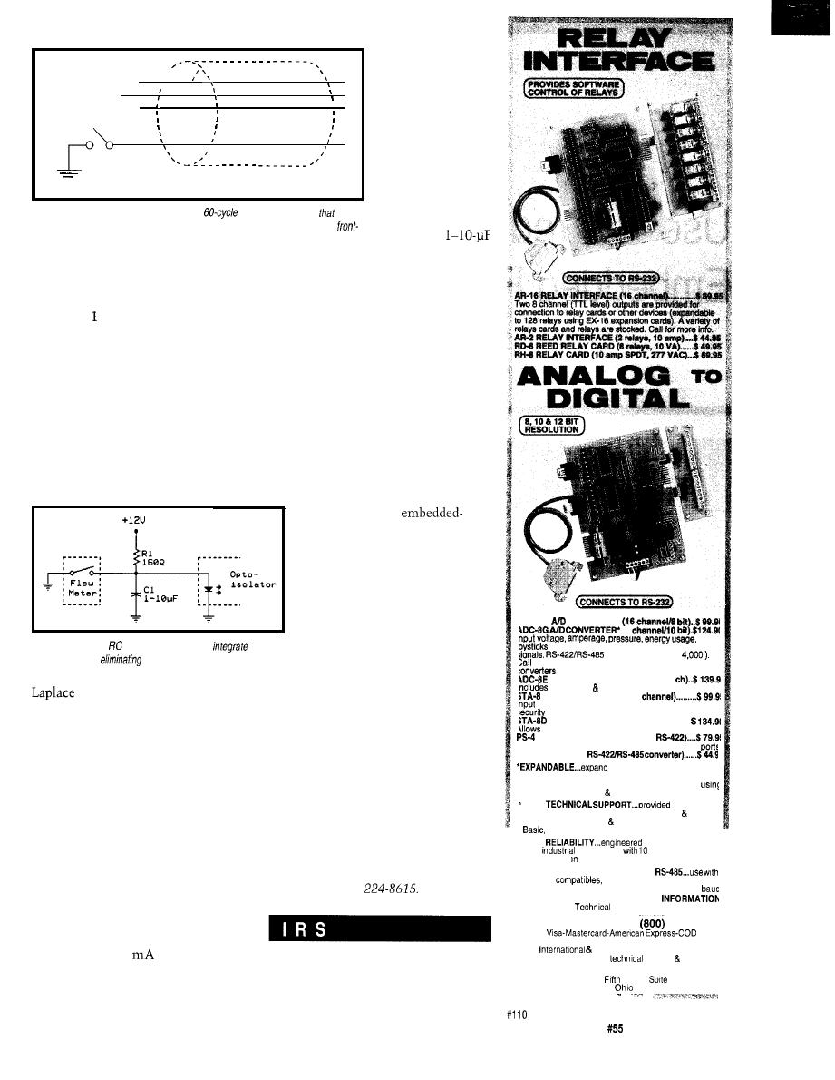
The flow-meter signal lead becomes a
low-impedance antenna when the
magnetic reed switch is open. The
induced AC waveform on the signal
lead can be as much as 2530 VAC
during this time. The waveform occurs
because of the capacitive coupling
between the conductors encased in the
conduit. The integrator input section
composed of and C3 in Figure 4
16
Issue
February 1995
Circuit Cellar INK
120 VAC
control
120 VAC hot
120 VAC
neutral
Flow
meter
250’
conduit
Figure 5-h industrial control applications,
noise from AC lines
are
often contained in the same conduit as the raw flow-meter output adds to the
able to dissipate up
to 0.9 W of heat
energy. I recom-
mend using a 5-W
resistor to keep the
temperatures
down.
The require-
ment of smoothing
of the AC wave-
form itself still
end filtering problem.
cannot handle this type of noise. This
inability combined with the AC
coupling of the 555 trigger input
through C means you are counting
60-cycle AC when the reed switch is
open.
Figure 6 is a simple, yet effective,
way to counter the induced noise from
the other conductors in the conduit.
You can calculate the exact values for
the pull-up resistor and filter capacitor
by mathematically modeling both the
signal conductor and the magnetic
reed switch. You can then solve their
remains. A
capacitor can do
this job, providing that you use just
enough capacitance to guarantee that
the LED in the optoisolator remains
biased in the on state when the
magnetic reed switch is open. The
pull-up resistor and smoothing
capacitor form an integrator for the
reed switch. This integrating action
removes the bounce on the opening
and closing of the reed switch.
CONCLUSION
When you interface counters to
real-world devices, you must be aware
of the environment you’re
Figure 6-A simple
circuit can be used to
the
flow-meter signal,
much of the induced AC noise.
transforms. This calculation
works quite well, but sometimes there
is a simpler way which yields the same
results.
But, these inputs can drive
you crazy when working with
high-speed counters. Sometimes
when it gets down to getting dirty, the
simpler the solution the better.
q
The problem is with the induced
AC waveform, which could be damped
out by placing a shunt resistor to
ground at the end of the signal lead.
Using a shunt resistor would work,
except it would have to be very small
and have a large current-carrying
capacity.
The other alternative is to simply
place a DC bias voltage on the signal
lead, which gives an offset to the AC
signal. A 160-R resistor tied to 12 V
provides up to 75
of current to
drive the LED in the optoisolator. Be
aware that the resistor will have to be
working in. Most
controller boards provide only
basic signal conditioning on their
optically isolated inputs. Unfor-
tunately, optically isolated
inputs are only fine when all
you’re looking for is an on/off
condition.
Bill Payne holds a B.S. in Computing
Sciences from the University of
Oklahoma, College of Electrical
Engineering. He has 12 years experi-
ence in the design of computer-based
equipment. He holds two semiconduc-
tor patents and has four others
pending. He is also a Novell Certified
Netware Engineer (CNE). He can be
reached at (918)
401 Very Useful
402 Moderately Useful
403 Not Useful
WC-16
CONVERTER*
(8
and a wide variety of other types of analog
available (lengths to
for info on other AID configurations and 12 bii
(terminal block and cable sold separately).
TEMPERATURE INTERFACE’ (8
term. block 8 temp. sensors (-40’ to 146’ F).
DIGITAL INTERFACE* (8
on/off status of relays, switches, HVAC equipment,
devices, smoke detectors, and other devices.
TOUCH TONE INTERFACE’................
callers to select control functions from any phone
PORT SELECTOR (4 channels
Converts an RS-232 port into 4 selectable RS-422
CO-485 (RS-232 to
your interface to control and
monitor up to 512 relays, up to 576 digital inputs. up to
128 analog inputs or up to 128 temperature inputs
the PS-4, EX-16. ST-32 AD-16 expansion cards.
FULL
over the
telephone by our staff. Technical reference disk
including test software programming examples in
C and assembly are provided with each order.
HIGH
for continuous 24
hour
applications
years of proven
performance the energy management field.
CONNECTS TO RS-232, RS-422 or
IBM and
Mac and most computers. All
standard baud rates and protocols (50 to 19,200
Use our 800 number to order FREE
PACKET.
Information (614) 464-4470
24
HOUR ORDER LINE
842-7714’
Domestic FAX (614) 464-9656
Use for Information,
support orders.
ELECTRONIC ENERGY CONTROL, INC.
360 South
Street,
604
Columbus,
432155438
Circuit Cellar
INK
Issue
February 1995
17
Jeff Fisher
Use Infrared to Make
Embedded Printing Easy
i. This is Mr.
We really like your
Frapdoodle 2000. Work us up a quote
on a container-ship load right away. By
the way, there’s just this one
there some way that it can print a log
of fraps on a little printer? Remember,
cost is our number one concern!”
“Sure, no problem. I’ll have a
quote for you in the morning.”
Click. Groan. Data logging.
Let’s see, a UART plus glue for serial
data (PC board re-layout!), a DE9
connector (case modifications!), a cable
to connect to the printer.. . Now,
where did I see those surplus
register printers advertised? I wonder if
I can find a case for them. Oh yea, and
a power supply. Groan.
“Where’s the aspirin?
Have you ever needed a little
printer for your stand-alone project?
We went through this recently and
discovered that it is more difficult and
expensive than it sounds. But instead
of telling you all the reasons you can’t
do it, I’ll tell you how some lateral
thinking may achieve the desired
results in an inconspicuous way.
CALCULATING AN APPROACH
You’ve seen these new personal
information managers
and
powered calculators? Many have
optional printers. All these printers
have a nonstandard method of connec-
tion. Many plug into the calculator or
PIM with a custom connector and
receive clocked-serial, TTL-level data.
But Hewlett-Packard uses a
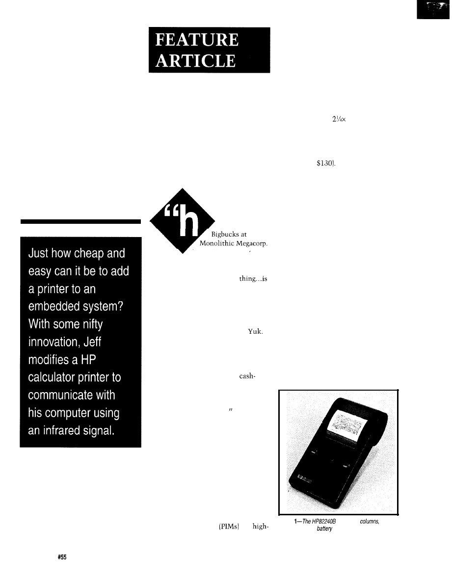
unique approach. Their HP82240
calculator printer (see Photo 1)
receives infrared signals from the
calculator. The printer has 24 col-
umns, prints on a
thermal-paper
roll, can operate on internal batteries
or a simple external power supply, is
available anywhere that sells HP
calculators, and is relatively inexpen-
sive (around
What could be better than a
wireless connection? All I need is an
infrared LED poking out somewhere, a
single bit from the micro to drive it, a
little software, and behold the printed
word! The interface cost is so low that
I could build it into every unit, and
then offer the printer as an option.
First, a little reverse engineering.
Now, I happen to know as much about
infrared as any other human being
alive, which is almost enough.
Nobody ever knows “enough”
about infrared. But, my tools served
me well in deciphering the infrared
codes, and I did
eventually
figure out
what the heck those extra bits on each
character were. Having done the hard
work, it turns out that the codes are
relatively easy to create.
ANATOMY OF A CHARACTER
Like most printers, the HP82240
receives eight-bit characters. The
Photo
printer-24
graphics capable,
or AC powered, wireless
infrared operation
18
Issue
February 1995
Circuit Cellar INK
lower 128 are standard ASCII charac-
ters. The upper 128 are special charac-
ters that include various symbols,
foreign characters, accent marks, and
so on. Escape codes offer expanded
(double-wide] printing, underlining,
and even dot-addressable graphics.
(This is all explained in the printer’s
manual.) If you are unfamiliar with
infrared, you should read the
on infrared communications before
going any further.
Character
Character “1”
Character “CR”
10.92 ms
ms 10.92 ms
10.92 ms
LRC Nibble
Data Byte
Character
840
Clock Bit
Data Bit
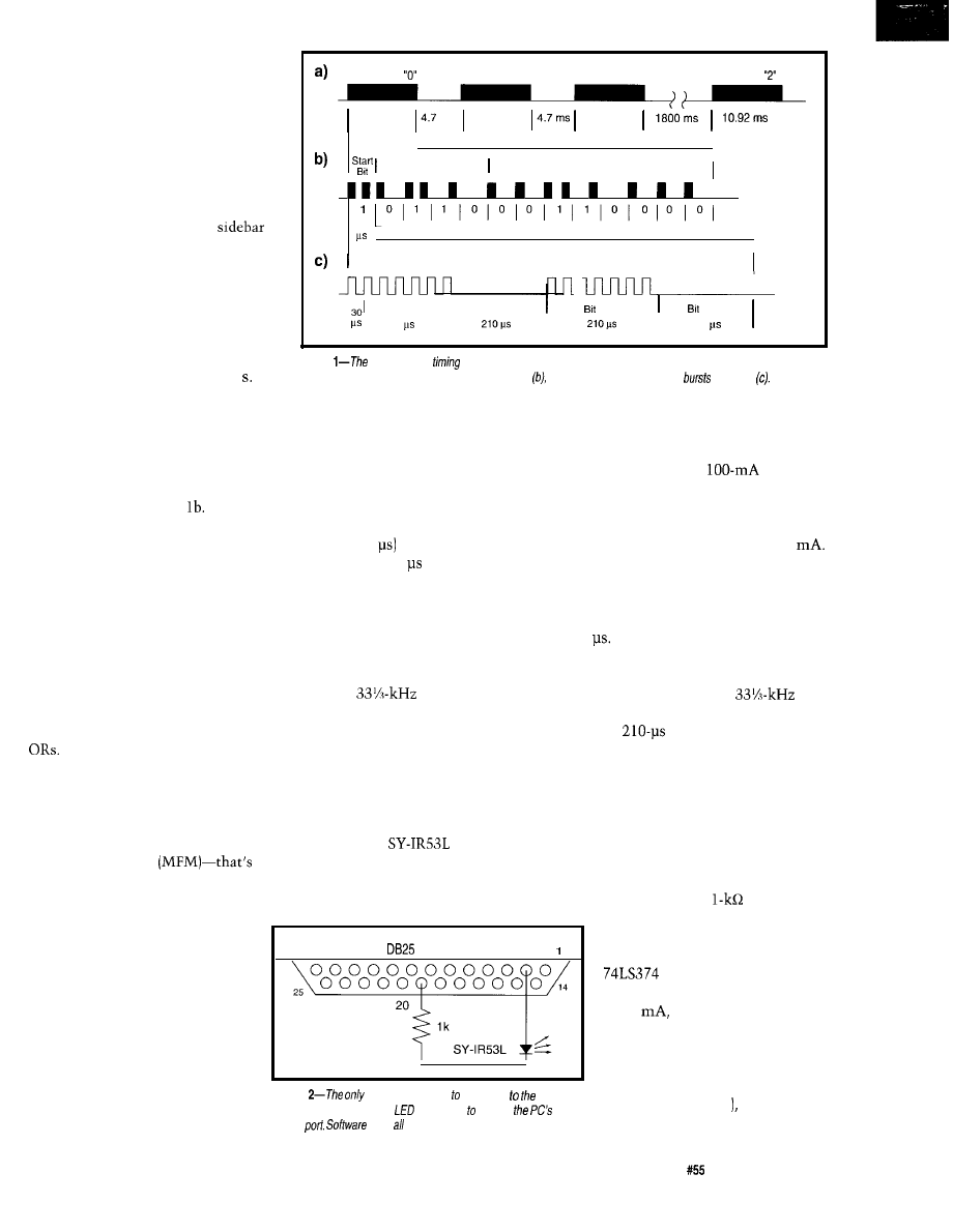
It takes 10.92 ms to transmit a
character (see Figure la). Each charac-
ter is followed by at least 4.7 ms of no
carrier. A carriage return causes the
printer to output the line and advance
the paper, which takes about 1.8
Since there is no feedback from the
printer, output must be paced so it
doesn’t overrun the meager printer
buffer. (Note that when the printer is
operated on battery power, it runs
slower as the batteries discharge.]
Bit cell 1
Bit cell 2
cell 3
cell
4
210
210
Figure
transmission
can be successively broken down into finer and finer pieces. Complete
characters
(a) can be divided info a series of bits
which are further described by
of/R
light
Now look at Figure Each
character consists of 13 bits. The start
bit (always a one) is followed by four
bits of longitudinal-redundancy check
(LRC) and eight bits of character. The
LRC and character bits are transmitted
high bit first. The LRC is calculated
using only the byte it is attached to.
There’s probably some kind of
giant polynomial expression that could
be used to create the LRC, but I
ignored this. Instead, I created a simple
procedure using bit tests and exclusive
(One of the advantages of reverse
engineering is that you get to avoid all
the theories and math that went into
the original design.)
bit cell (840
is divided into four
l
for a clock pulse, if the previous bit
pieces, each 210 long. The second
and fourth piece always have no carrier
was zero, if it is the start bit, or if
present. The third piece is the data bit
and has a carrier present if the data bit
the previous bit was the start bit,
is on. The first piece is where the
clock pulse goes, but it is only inserted
turn the carrier on at the start of the
if the preceding data bit is zero.
bit cell.
As you can see in Figure lc, each
The
carrier can run
seven cycles in 210 us, which is just
long enough for the detector to trigger
and the main reason that the printer
only works at desktop distances from
the transmitter.
results (over three feet) at only 2.5
use an appropriate series resistor to
So, all you need to drive a printer
from your embedded system is a single
TTL output bit and a processor fast
limit the current. Alternatively, you
enough to turn the bit on and off every
can use some discrete parts to drive
15
If you can’t dedicate your pro-
cessor to driving the LED during print-
ing and 15 us is too fast to handle with
the LED closer to its
rating.
interrupts, you can add a
oscillator, which you enable and dis-
Just be aware that stronger is not
able on
intervals. The fre-
necessarily better in the bizarre world
quency doesn’t have to be precise, so a
555 or ceramic oscillator is adequate.
of infrared. I obtained successful
The bits are transmitted using a
technique similar to modified fre-
quency modulation
right, the same scheme used in many
disk drives! The advantage of MFM is
that it is self-clocking, well
understood, and reliable. Note
that MFM modulates the fre-
quency of pulses, not the fre-
quency of the carrier. The rules of
this peculiar style of MFM are:
INFRARED LEDS
I like the
infrared LED
available from Radio Shack (276-143).
You can drive this LED satisfactorily
from many TTL parts as long as you
A SIMPLE EXAMPLE
So much for theory. Now to really
do something.
13
Male
2
l
for a data pulse, if the data bit is
one, turn the carrier on in the
middle of the bit cell. Other-
wise, leave the carrier off in the
middle of the bit cell.
For this example, we used an IBM
PC-compatible computer. We connect
the infrared LED and
series
resistor to data bit zero of the
parallel port (see Figure 2). Most
PCs use an octal latch such as the
for the parallel port’s
data bits. This part can source up
to 2.6
which is adequate for
this example. The hardware is
that simple! Software in the PC
can now drive the infrared LED.
Figure
hardware required send data infrared
printer is a resistor and an
connected a bit on
printer
does the work.
Character
Bit
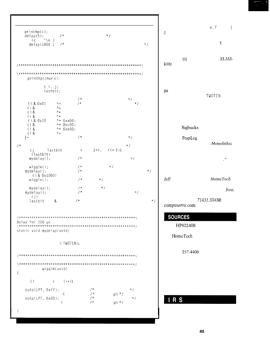
The example program,
p
r i n t
h p (Listing 1 is written in
Turbo C. It reads input and sends
Circuit Cellar INK
Issue
February 1995
19
You heard right. A quality C
compiler designed for the 8051
microcontroller family, just $99,
including the Intel compatible
assembler and linker.
And a
s o u r c e
level simulator is also
available,
just $79.
A great
companion to our fine Single
Board Computers, like those
below.
CALL NOW!
a ‘51 Compatible Micro
40 Bits of Digital
8 Channels of 10 Bit A/D
3 Serial Ports
or
2 Pulse Width Modulation Outputs
6 Capture/Compare Inputs
1 Real Time Clock
64K bytes Static RAM
+ UVPROM Socket
512 bytes of Serial EEPROM
1 Watchdog
1 Power Fail Interrupt
1 On-Board Power Regulation
Priced at just $299 in single
quantities. Call about our
C Development Kit, just $449.
versions of the
hove processors
vith on-chip capture registers,
EEPROM, A/D
more. Call or ftp for o list!
as as $49
Equipment Corp.
S i n c e 1 9 8 3
( 6 1 9 ) 5 6 6 - 1 8 9 2
info@hte.com
Internet ftp:
INFRARED COMMUNICATIONS
The most confusing part about infrared data transmission is that there
are three frequencies involved.
The highest frequency, more appropriately called wavelength, is the
infrared light emitted by the LED. For most consumer remote controls [and
this calculator printer), the wavelength is around 880 nm. This wavelength
is in the near infrared band-somewhere between visible light and actual
heat radiation. You should choose an infrared LED that emits in a range of
850-900 nm.
The next highest frequency is that of the carrier. The carrier more
reliably detects the infrared turning on and off at a known frequency than
trying to detect a steady state on or off. This makes sense since everything
emits infrared energy, so the background level is constantly going up and
down. Typical carrier frequencies range from 20
to 80
with 40
being most common. Since the receiver circuits are pretty simple, the
carrier can often vary by as much as 20% and still works.
The next lowest frequency is used for the pulses that carry the actual
information. Most infrared data is transmitted by turning the carrier on
and off at times determined by the data. This method results in pulses of
the carrier, followed by no carrier, and is called Pulse Code Modulation
(PCM).
Both the on and off times can vary to carry data, so the frequency of
the pulses is not necessarily constant. Usually, only the on or off time is
varied to keep things simple. Since it may take many cycles for the
receiver to react to the carrier, the on times are usually at least ten times
longer than the carrier wavelength. Thus, the pulses are usually measured
in hundreds of microseconds of on and off time.
Listing
l--This sample program
printing on the
printer. reads from
standard input.
#include
Ox378
Ox278
LPT
#define THIRTY 6
which printer port to use
adjust to get
carrier
#define
55
adjust to get 210 delay
static unsigned short counter:
/XX************
static void
static void
static void
\****************x*****************************************,
int
char
char c;
initialize the delay system
+ 2,
enable output on parallel port
while
!=
(continued)
Issue
February
1995
Circuit Cellar INK
Listing l-continued
if ==
intercharacter gap
add about 1.8 seconds delay after CR
return 0;
Print a single character on the HP infrared printer
void
unsigned int i
static int
i = c;
put in the character
if
i 0x300: put in the check nybble
if 0x02
i
0x500;
if 0x04
i
0x600;
if 0x08
i
0x900;
if
i
if 0x20
i
if 0x40
i
if 0x80
i
0x700;
i 0x1000:
put in the start bit
rotate it all out: start-bit, check-nybble, char
for = 0,
= 0; j 13;
i
if
no clock pulse needed
else
clock pulse
wait until middle of bit cell
if
on bit
else
off bit
fourth part of bit cell
if
= i 0x1000; save bit for clocking next pass
counter = 0;
while (counter++
Wiggle the output bit 7 times to create a carrier
static void
int i:
for = 0; i 7;
counter = 0;
turn the bit on
while (counter++ THIRTY/Z); wait 15
turn the bit off
while (counter++ THIRTY);
wait 15
each character to the printer. It is
meant to be used as filter in a com-
mand-line pipe (e.g., type
i 1 e
r i n t. h p).
The main routine handles
the reading of characters and gross
timing issues. The routine p r i
n h p
encodes and outputs the characters.
The
mydel ay
routine pauses for 210
ps, and w i
1 e
creates a brief
carrier pulse.
Ifyouwanttorunprinthp,you
need an oscilloscope or logic analyzer
to calibrate the two routines. First, get
the carrier cycle length as close to 30
as possible by changing the
TH I RTY
definition. Then, adjust
so
the
gap between the first two carrier
pulses is as close as possible to 210 ps.
This should get your printer working.
THENEXTDAY
“Mr.
again. Thanks for
the quote and the demonstration of
your new
option last week.
But, uh, about the order..
Megacorp was just bought out by
Polylithic Gigacorp. It seems that
Polylithic just don’t give a frap..
Click. Oh, well. At least some of
our real customers will appreciate it.
q
Fisher is president of
Solutions, a home automation
manufacturer and retailer in San
California. He may be reached at
(408) 25 7-4406 or
The
printer is available
from:
Solutions
10570 S. De Anza Blvd.
Cupertino, CA 95014
(408)
Fax: (408) 257-4389
Hewlett-Packard
Portable Computer Division
1000 NE Circle Blvd.
Corvallis, OR 97330
(503) 757-2000
404
Very Useful
405 Moderately Useful
406 Not Useful
Circuit Cellar
INK
Issue February 1995
21
It’s Not Just
for Memory
Anymore
An
Introduction
to PCMCIA
J. Gastriani
t
was
around the
curious musicians started
wondering about those “funny little
connectors” found on the back panel
of high-end synthesizers and sampling
keyboards. Accessory catalogs were
studied; inquiries were made.
Soon, they learned that expansion
cards could be obtained and plugged
into those sockets. By issuing the
correct commands, keyboard param-
eter sets or “patches” as well as wave-
form data could be saved to the small
memory cards and recalled later. The
fact that these cards could be inserted
or extracted while the unit was run-
ning made them even more attractive.
The offspring of those funny little
sockets have now found their way
onto virtually every notebook com-
puter made today. The devices, which
plug into these sockets, grew out of
the JEIDA (Japan Electronics Industry
Development Association] standard
and are now known as personal com-
puter cards or simply PC cards. These
credit-card-sized peripherals contain
anything from real-time global posi-
tioning systems to tiny hard drives
with rotating media. Even more preva-
lent now are high-speed modems,
which enable people on the road to
“jack in” to that Infobahn we keep
hearing about.
The computer industry is just
beginning to see the benefits and
potential of PC cards. For about the
last three years, the standard for these
devices and the system software that
controls them, collectively referred to
as PCMCIA (Personal Computer
Memory Card International
tion), have quickly become more
known to both manufacturers of
computers and end-users alike. As it
now rolls into its latest 3.0 incarna-
tion, the specification has endured the
test of time and public scrutiny.
After a slow start, great strides
have been taken in discovering the
essential criteria which enable the
cards to operate on a particular host
and also provide the foundation for
successful real-world, cross-platform
operation. Although we’re not there
yet, this achievement will provide us
with what is known in the industry as
interoperability.
Already, we are at the point that a
notebook computer is considered
stripped down if it doesn’t contain at
least one PCMCIA socket. What’s
more, PCMCIA cards are sold every
where from giant, computer-ware-
house stores in your neighborhood to
the shop-at-home cable channels.
Consumers are asking manufacturers
of desktop systems to provide PC-card
capability as part of their solution on
subnotebooks as well as desktops.
Perhaps, we may soon see sockets on
everything from automobiles to public
telephones.
In the embedded world, PCMCIA
sockets and cards offer a whole new
breed of device. Designers can simply
add a socket or two to their designs
along with the proper enabling firm-
ware, and flexibility and future expan-
sion is possible.
But, let’s take a closer look at
PCMCIA.
HARDWARE
Sockets are the basic receptacle
PC cards are inserted into and removed
from. The socket connector itself
normally rests inside the host com-
puter and consists of a plastic housing
with a double row of 34 pins giving a
Thickness (mm)
3.3
II
5
10.5
IV
13.5
Table
Type
is a nonstandard form factor,
which
rejected,
but is used by some manufacturers.
22
Issue
February 1995
Circuit Cellar INK
Photo
Type
card
houses the
media
hard drive.
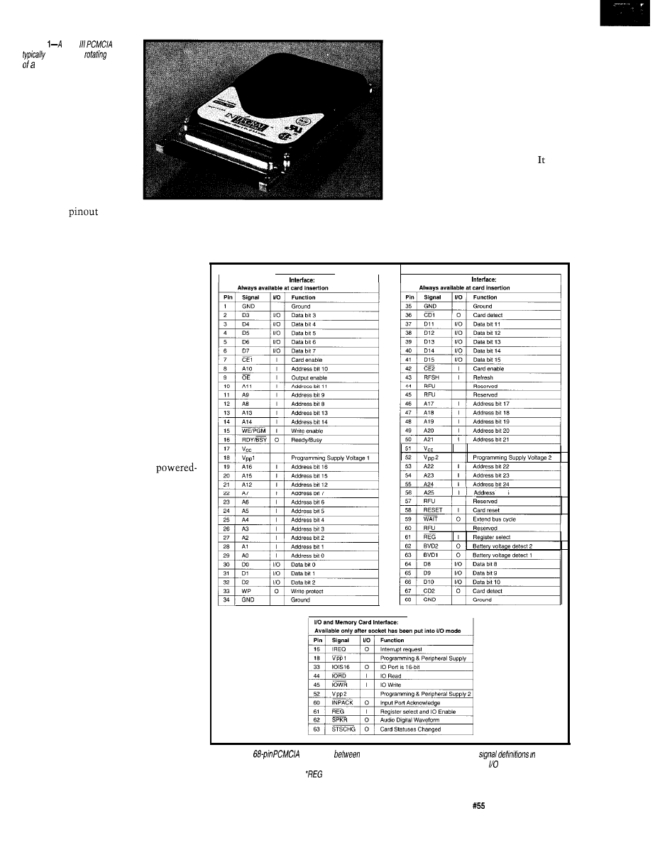
total of 68 pins, each
spaced 1 mm apart.
Photo 1 and Figure 1
illustrate the pin layout
in a PCMCIA card end.
The exact
of the
socket can be found in 4.2-4.3 of
PCMCIA PC Card Standard Release
2.01.
Cards are inserted into and ex-
tracted from the sockets while the
host’s system power is active, a tech-
nique also known as hot swapping.
Hot swapping and the whole notion of
temporal devices in personal comput-
ers is a fairly new concept and as such
has its own unique set of problems.
These problems center mainly on the
fact that, until now, system resources
were allocated to devices present at
system bootstrap. The devices stayed
present throughout the duration of the
computing session, remaining nearly
entirely static until the session was
terminated.
Plugging a PC card into a
up system and expecting the function-
ality of the card to suddenly become
active is quite an expectation. How
this is done is where the real magic of
technology lies.
If you were to look crosswise at
the socket pins, you’d see that some of
the pins do not protrude as far as
others. The power rails are located on
the outermost pins and are the longest
of the pins. When a card is inserted,
they make contact first. Similarly,
when it is extracted, they retain the
longest. This power arrangement
enables buses to be powered up and
tristated when (or very soon after) the
card is inserted.
In addition to data and address
lines, there are also control lines,
battery indicators, a single interrupt
line, and a card-detect line, which can
indicate card insertions and extrac-
tions.
To be able to insert a modem card,
have the OS recognize and configure it,
spawn a communication program,
connect to an on-line service, down-
load E-mail, and then disconnect is an
amazing series of events. To make the
scenario even more interesting, re-
move the modem card and insert a
120-MB, rotating hard drive containing
a customer database, which launches
an invoice program.
The interface between the
socket’s 68-pin bus and the host is
known as the socket controller.
manages the low-level aspects of the
socket (i.e., power, interrupt routing,
memory and I/O window allocation,
etc.) according to program control.
On desktop and notebook sys-
tems, the socket controller is typically
a dedicated chip which is part of some
Memory
Only
Card
Memory Only
Card
bit 25
Figure l--The
interface
a PC card
and its socket shows the
memory
mode. The lower tab/e describes those pins whose functions change when the socket is in mode. The mode is
determined by the state of the
signal.
Circuit Cellar INK Issue
February 1995
2 3
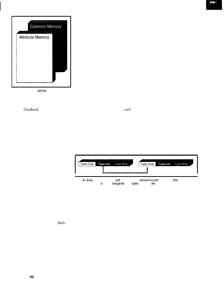
Figure 2-Common and
memory share the
same address space. The client selects which one is
active.
sort of host
adapter.
The Intel 82365SL
and the
86082 are examples
of popular socket controllers.
In embedded systems, the socket
controller can be implemented with
discrete logic, as one of the standard
pieces of silicon, or as a single task
running along with other tasks in the
microprocessor. As another possible
route, you could use a dedicated
microcontroller like the PIC.
RESOURCES
As I mentioned, the key to en-
abling PC cards in a system is to
provide them the resources they
require. However, before I talk about
how a card tells the system what
resources it needs, let’s take a look at
the various categories of resources
available on a host.
Power is the most obvious and
most basic resource. It is provided to
the card via the power rails and is
typically 3.3 or 5 V, depending on the
host system. A typical socket control-
ler may be requested to provide higher
voltages for certain cards (e.g.,
memory cards, which usually require
12 V for programming). To switch the
power rails to the card, the socket
controller either has built-in active
switches or external MOSFET devices.
To interface a particular card’s
function to the rest of the system,
memory windows are created which
map a particular region of the card’s
address space into the host system’s
address space. The exact place within
the host map is determined by system
software. The size of the memory
window as well as its attributes are
usually also programmable.
On systems with I/O space, a
card’s I/O decoding might require
connection to a particular range of I/O
locations. This is particularly critical
when a PC card is set up to emulate a
static device.
Another important resource
sometimes applicable is the PC card’s
interrupt routing. Refer again to Figure
1.
Notice that a card has only a single
IREQ line which can be routed
through the socket controller to any
host interrupt line. This routing is
usually programmable, allowing for
flexible compatibility.
The IREQ signal from the card
should not be confused with the
detect interrupt from the socket,
which is used for insertion and extrac-
tion detection and has nothing to do
with the card’s IREQ signal. Instead,
the IREQ line is to be used by the card
in a card-specific manner.
While the currently released
PCMCIA specs do not include support
for DMA to and from a PC card, the
fourth type of card, which they call
Type IV. Although the Type-IV form
factor was rejected by the PCMCIA
committee, the 13.5mm slot can be
found on some Toshiba models. Table
1
shows the correlation between
thickness and type.
MEMORY SPACE
As Figure 2 illustrates, there are
two types of memory space on a PC
card: common and attribute. Even I/O
cards must implement attribute
memory for this is where the card’s
CIS (card information structure) is.
The CIS contains the card’s “biogra-
phy” as well as its “wish list” for
system resources.
By definition, when a card is
powered up, it initializes in memory
mode. This ensures that as each card is
inserted, it begins in a known state.
This state can best be characterized as:
l
memory mode active [as opposed to
I/O mode active)
l
attribute memory active (as opposed
to common memory active)
Attribute and common memory share
the same address space (64 MB), but
only one can be active at a time. The
Figure
card has information
info if detailing ifs
number, and
items. The
information is conveyed fhe host
use of
which form basis for a linked list of data objects
next release (version 3.0) accommo-
dates it. Socket controllers are already
appearing which have the ability to
provide DMA channels to and from
the card’s address space. Until the
DMA functionality of the PCMCIA
software layers are standardized, DMA
implementations are ad hoc.
CARD FORM FACTORS
There are currently three types or
configurations of PC cards recognized
by the standards: I, II, and III. The
primary difference between the types
is the thickness of the card.
The Japanese consortium of card
standards (JEIDA) has taken a small
lead in this area having designated a
socket controller provides the means
to select one of the two memory
spaces.
Attribute memory is typically
(although not always) nonvolatile,
contains the CIS, and if applicable, the
configuration registers. Attribute
memory must begin at offset 0, but
need not be in a single contiguous
region. Most cards implement their
CIS and configuration registers at
fairly low offsets in attribute space
(according to PCMCIA guideline),
which ensures addressability by all
hosts. This also minimizes that
amount of page mapping required by
the system software to access these
regions.
26
Issue
February 1995
Circuit Cellar INK
A quirk of attribute space is that it
is a
interface only. In other
words, when reading CIS information
or writing configuration registers, only
the even bytes are considered valid
data. Likewise, on write cycles, the
card is only obliged to handle writes to
the even bytes.
Mass storage PC cards have a
separate memory space called common
memory, which provides the main
write/read memory space for the card.
In a 4-MB SRAM card, for instance,
common memory is viewed as a
linear region. By setting up a mapping
window and by manipulating the
offset addressed by this window into
common memory, any byte contained
on the card can be accessed.
Common memory is treated as an
S-bit array of bytes. Both the even and
odd bytes are valid.
CARD INFORMATION
STRUCTURE (CIS)
The Card Information Structure is
implemented in a format known as the
metaformat.
As mentioned, the CIS is
the card’s biography, which contains,
among other things, the:
l
manufacturer
l
part number
l
voltage and current requirements
l
absolute maximum ratings
l
one or more configuration scenarios
(I/O cards only)
In theory, when a card is inserted,
system software powers up the card
and starts looking at the CIS. As the
CIS is traversed and parsed, more
information about the card may be
obtained.
This information is conveyed to
the client through the use of
Tuples form the basis for a linked list
of data objects which provide enough
information about the card that it may
be properly enabled and used. Figure 3
presents the layout of a tuple.
As you can see, layer
1
offers the
basic compatibility tuples. The first
byte contains the tuple code and may
fall into the range of
(hex). The
values between
and 3F are re-
served for future expansion. Layer 2 is
for data recording format and lies
HUGE BUFFER
FAST SAMPLING
SCOPE AND LOGIC ANALYZER
C LIBRARY W/SOURCE AVAILABLE
POWERFUL FRONT PANEL SOFTWARE
DSO Channels
2
Ch. up to 100
1 Ch. at
4K or 64K
Cross Trigger with LA
125 MHz Bandwidth
Logic Analyzer Channels
$1799 DSO-28204 (4K)
$2285 DSO-28264 (64K)
8 Ch. up to 100 MHz
4K or 64K
Cross Trigger with DSO
PAL
GAL
EPROM
EEPROM
FLASH
MICRO
etc..
Free software updates on BBS
Powerful menu driven software
up to 128 Channels
up to 400 MHz
up to
Samples/Channel
Variable Threshold Levels
8 External Clocks
16 Level Triggering
Pattern Generator Option
LA12100 (100 MHz, 24 Ch)
LA32200 (200 MHz, 32 Ch)
LA32400 (400 MHz, 32 Ch)
$2750 LA64400 (400 MHz, 64 Ch)
Call (201) 808-8990
Link Instruments
369
Passaic
Ave, Suite 100, Fairfield, NJ 07004 fax: 808-8786
Circuit Cellar INK Issue
February 1995
27
between 40 and 45, Layer 3 provides
the CIS and a configuration scenario
data organization and is in the range of
which makes sense for the host at that
and Layer 4 offers
particular time. After configuration is
specific features and is found in
selected and set, an I/O card then
The special value FF present as either a
assumes I/O mode. The changeover at
tuple code or a link marks the end of
the socket level between memory and
the tuple list. Table 5.2 of section 5.7
I/O mode causes a few pins to be
of the PCMCIA PC Curd Standard
redefined. Consult Figure
1
for the
describes all tuple codes and their
differences in pin definitions between
meaning.
memory and I/O mode.
This scheme is quite flexible and
allows for simple or complex CIS
structure. Special tuples (long links)
allow the CIS to span attribute and
common memory space, thereby
enabling elaborate CIS schemes to be
implemented.
Lately, some of the newer cards
coming out have two or more separate
and distinct functions. For example,
Card Clients
CARD FUNCTIONS
Memory cards are the simplest of
PC cards to configure. They typically
require only power for reading, writ-
ing, and mapping a window. In the
case of nonvolatile memory like flash,
special programming of voltage and
current requirements can be found in
the card’s CIS.
Layer
I/O cards are the most prevalent of
PC cards. By far the most popular I/O
card is the modem or fax/modem card.
I/O cards may or may not require I/O
windows to be set up for them through
the socket controller. When I/O is
needed, only certain I/O locations are
allowed to be decoded by the card.
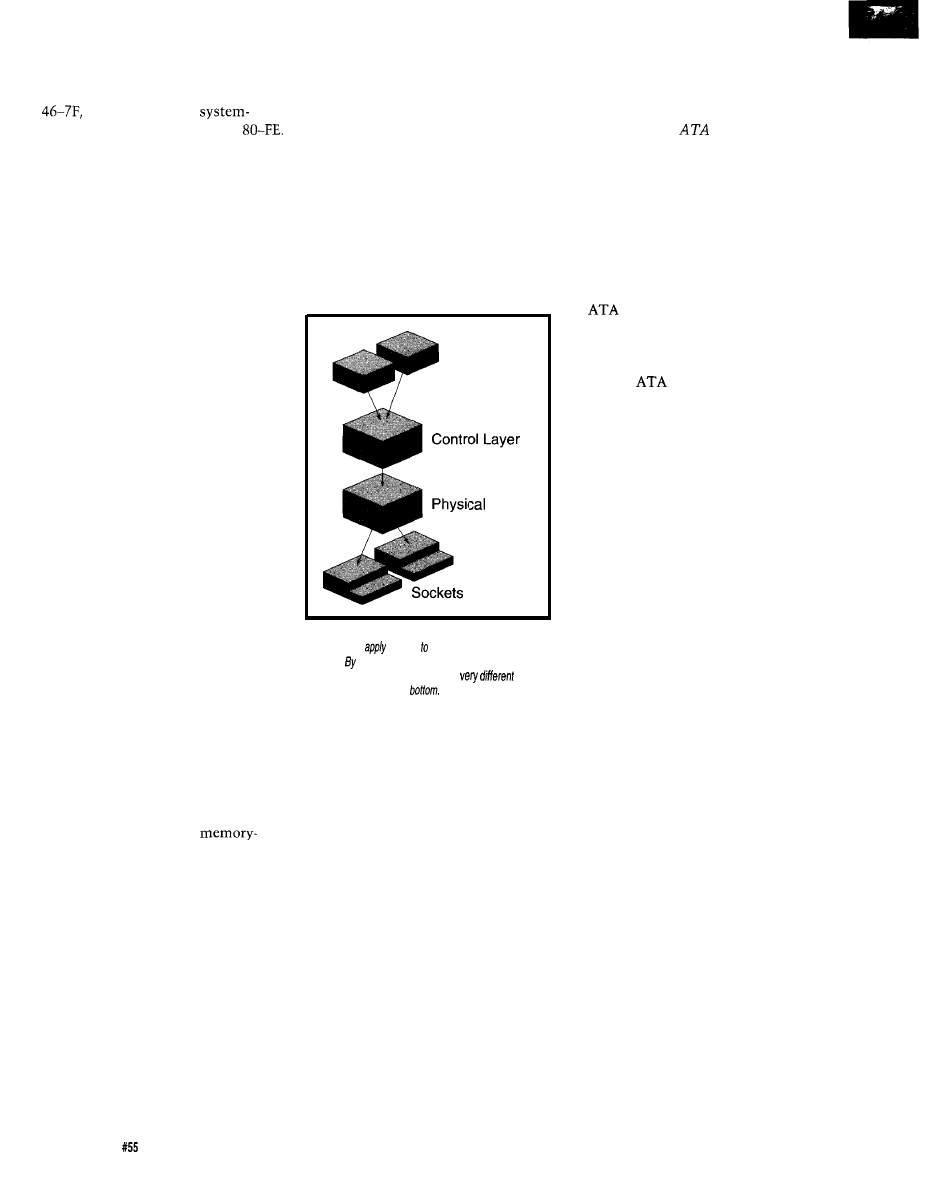
Figure
4-PCMCIA
software is broken
into several
layers which
mostly desktop and notebook
systems. using separate layers, it’s possible to have
a common interface at the top and
physical devices at the
This technique enables a PC card
to look like any device that would
normally be attached to a particular
host’s bus. By setting up the proper I/O
windowing, the I/O card’s register set
can be made to respond to host bus
requests within certain ranges.
Xircom has developed an Ethernet/fax-
modem card, which combines a minia-
ture Ethernet adapter and a high-speed
fax/modem. Through this type of
arrangement, both of the card’s func-
tions share the same socket.
Some I/O cards have
mapped registers, which are present in
either the card’s common or attribute
memory space. By supporting this kind
of operation, a particular card can
ensure interoperability (or at least a
higher chance of achieving it) by
working in systems that have I/O
space (e.g., the Intel x86 series) or
those that do not (e.g., the Motorola
68k series).
This multifunctionality poses
some challenges in the area of inter-
rupt routing since there is only one
IREQ pin from the card. This one
IREQ pin, which is routed to one of
the host’s interrupt lines, must be able
to signify an interrupt from two or
more separate sources.
All cards, when first powered up,
assume memory mode. This facilitates
the reading and parsing of the card’s
CIS. The client selects a particular
configuration based on information in
Some new proposals are being
discussed by PCMCIA which include
the use of virtual sockets to “house”
the second and subsequent functions
on a particular card. However, at this
time, there have been no ratified
extensions or enhancements to the
specifications for multifunction cards.
28
Issue
February 1995
Circuit Cellar INK
Still another class of PC cards are
those that appear to the system to be a
standard peripheral known as an AT
attachment or an
device. These
cards may contain solid-state memory
or rotating media. When the card’s
resources are properly configured, the
card appears as a hard drive.
In a typical desktop or notebook
application, these devices are con-
nected to the host file system by a
device driver and appear as another
logical device. In an embedded system,
an
device could contain the
operating system (with a virtual
memory-storage partition) and/or extra
storage.
Many
devices contain
programmable watchdogs. These
enable the power management aspects
of a particular OS to set timeout
values for spinning down the drive
during periods of inactivity.
SOFTWARE
Whether the environment is
desktop, notebook, or embedded, the
general intent of PCMCIA software at
large is universal:
l
enable cards within sockets
l
protect systems from bad cards when
possible
l
encapsulate the details of socket
electronics
l
allow many clients of sockets to
coexist
l
manage resources
l
provide interoperability and compat-
ibility
How these goals are best achieved
is almost entirely platform specific.
But, the basic tenets are the same. By
breaking up the software into layers
and by defining each layer’s boundaries
and the part that layer serves greatly
simplifies the conceptual visualization
of implementing solutions.
PCMCIA software is broken up
into two basic areas: clients and serv-
ers. The server layers provide the
services to the socket controller.
Clients, on the other hand, interact
with the servers and other clients in an
effort to configure the cards and keep
them running.
Layers, outlined in the PCMCIA
documents under socket services and
card services, apply mostly to desktop
and notebook systems. Figure 4 pre-
sents the various layers which make
up PCMCIA software.
The physical layer controls the
hardware registers or other program-
ming model of the socket controller(s)
on a particular platform. In essence,
this layer reports the capabilities of
each socket controller and enables the
encapsulated manipulation of them.
A simple interface to higher-level
layers allows these higher layers to
deal with logical sockets. The
PCMCIA standard calls this layer
socket services. There may be one or
more of them in a system, each han-
dling one or more socket controller(s).
Above the physical layer lies the
control layer which reacts to events,
manages resources, and interacts with
the card clients in a system. This layer
is part of the operating system and
contains further abstractions that, at
this level, enable memory technologies
to be encapsulated according to their
topology and power requirements.
Each client makes resource re-
quests to this layer. Each request is
weighed against collisions with other
system components; collisions cause
rejections. This layer is called card
services in PCMCIA’s standards. There
is only one case of it in any system.
Clients are tasks at the top of the
PCMCIA food chain. When a card is
inserted, the ensuing interrupt is
handled by the physical and control
layer. This eventually causes an inser-
tion event or message to be broadcast
to all clients registered with the con-
trol layer.
At this point, a client typically
parses the card’s CIS looking for either
recognizable “landmarks” within the
manufacturer’s ID tuple or moving
right into the configuration tuples.
Once it starts configuration, it con-
structs resource requests and passes
them off to the control layer.
This process continues until a
particular configuration scenario is
accepted by the control layer, at which
time it is latched and the card is
enabled. The card remains in this state
until it is either extracted or some sort
of power-management message is
broadcast, forcing the card and socket
into a lower-power state.
Extracting the card reverses the
process so that resources are freed and
given back to the host.
CONCLUSION
PCMCIA technology opens doors
in many areas of desktop, notebook,
and hand-held computing. This intro-
duction provides a foundation for
further study. In a follow-up article, I
will focus more intensely on embed-
ded systems, detailing an actual appli-
cation of PCMCIA.
Lalo Gastriani is a consulting
engineer based in Southern California.
Since 1982, he has concentrated on
real-time software architecture and
design. Since 1990, he has been
involved in PCMCIA. Lalo may be
reached at
or P.O.
Box 80801,
Santa Margarita,
CA 92688.
PCMCIA specifications:
Personal Computer Memory
Card International Assoc.
(
P C M C I A
)
1030G East Duane Ave.
Sunnyvale, CA 94086
(408) 720-0107
Fax: (408)
PCMCIA peripherals:
Integral Peripherals, Inc.
5775 Flatiron Parkway, Ste. 100
Boulder, CO 80301
(303) 449-8009
Fax: (303) 449-8089
Xircom
26025 Mureau Rd.
Calabasas, CA 9 1302
(818) 878-6423
Fax: (818) 878-7630
407 Very Useful
408 Moderately Useful
409 Not Useful
P
RECISION
F
RAME
G
RABBER
Corporation
Vision Requires Imagination
800-366-9131
97075 USA
,
the CXlOO
video frame
grabber OEM, industrial and
applications. With sampling jitter of only
and video noise less than one WB,
breaks new ground in imaging price/perfor-
mance. The CXlOO
is a rugged, low power, ISA
board
rock solid, crystal controlled
timing and all digital video synchronization.
A
Software developers will appreciate the simple
software interface, extensive C
and clear
documentation. The CXlOO is a
com-
patible, drop-in replacement for our very
popular Cortex I
grabber.
A
today
for complete specifications and volume pricing.
F
OR
CXlOO FEATURES
n
Crystal
Image Accuracy
. Memory Mapped, Dual-Ported Video RAM
n
Programmable Offset and
. Input, Output and Overlay
n
Resolution of
5 12x486 or Four Images
of 256x243 (CCIR 512x512 256x256)
. Monochrome, 8 Bit,
Tie
Grabs
. Graphics Overlay on
or Still Images**
n
External Trigger Input
. RGB or
Hz Interlaced Display
.
Auto Detect, Auto Switch
. VCR and Resettable Camera Compatible
. Power Down Capability
n
BNC or RCA Connectors
. Built-In Software Protection**
Function C Library with Source Code
. Text Graphic Library with Source Code
. Windows DLL, Examples and Utilities
. Software also available free on our BBS
. Image File Formats:
PIC,
and
COST
*
Circuit Cellar
INK
Issue
February
1995
2 9
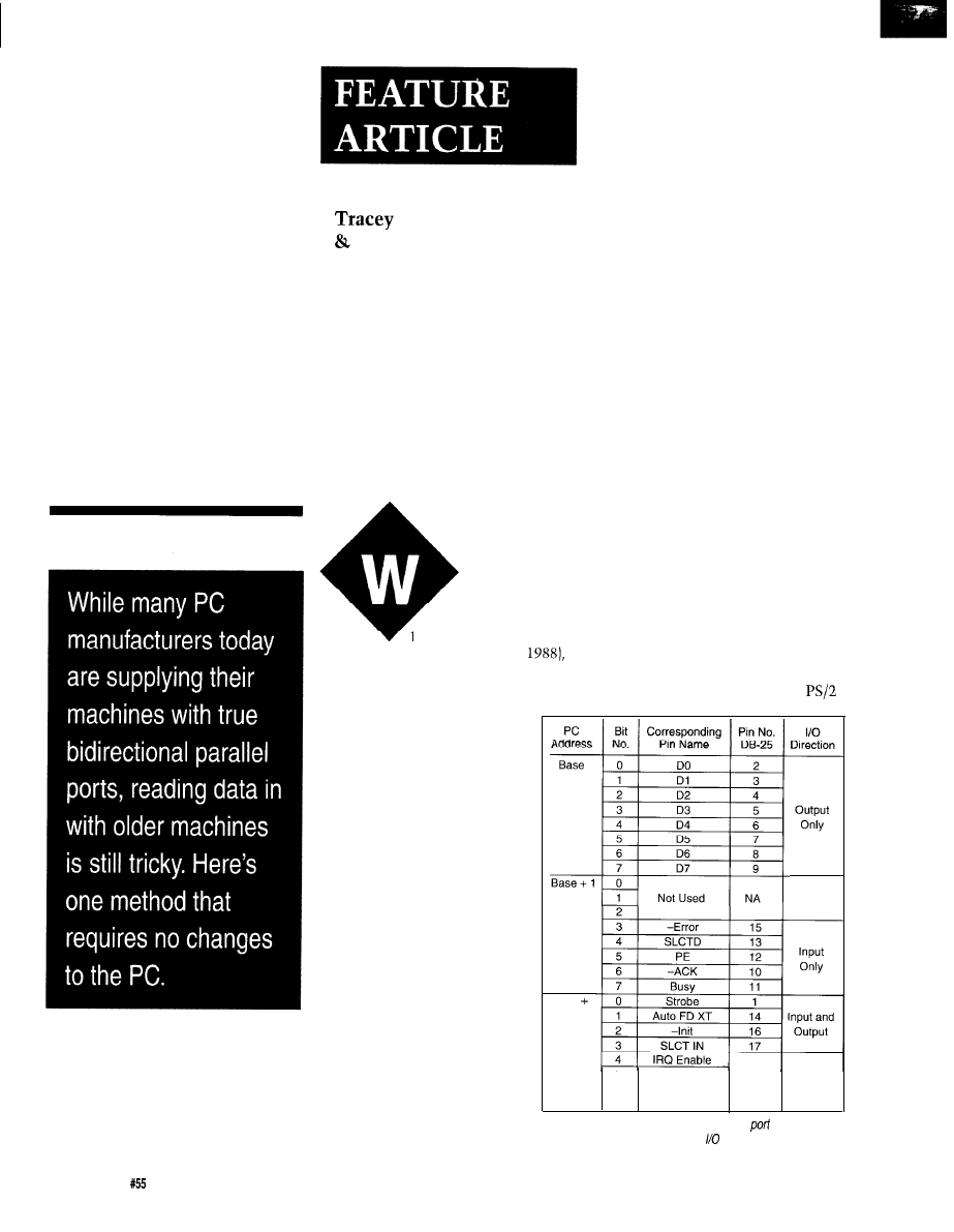
Lee
Kok-Leong Ong
Speeding and Slimming
Your Port Access
A Different Way of Reading
from the PC Parallel Port
hen we came
across the DDT-5 1
805 1 emulator project
presented by Steve
Ciarcia several years ago (BYTE
we decided to improve on his imple-
mentation. The DDT-51 communi-
cates with the PC using its
parallel printer port. Steve
modified a standard port for
bidirectional operation, but we
wanted to use an unmodified
port. We decided to forego the
soldering iron in favor of a
software solution.
We chose to read data a
nybble at a time, using one of
the other parallel port pins to
indicate which of the two
nybbles transferred. Of course,
the software later combines
both nybbles. This method
slows down data transfer,
especially if the software is
written using a high-level
language, and uses one extra
pin of the port interface. What
is more important, however, is
that the port and device have
to make that one extra connec-
tion. This means that cable
and connectors have to be one bit
wider.
To accomplish this variation,
software handling the transfer needs to
generate a READ signal using one of
the parallel port pins. We explored the
possibility of using this signal to
indicate the order of nybble read.
Assuming a negative logic READ, our
solution was to use the low level
(active) to indicate one nybble and to
use the high level (inactive) to latch
the data and gate the next nybble to
the interface.
Thus, we save the two instruc-
tions needed to manipulate the nybble
indicator bit in Steve’s approach. We
also save on one extra connection and
do not have to perform surgery on the
parallel card as suggested by Steve.
By the way, although we use the
DDT-5 1 as our example, we under-
stand that it has been discontinued as
a product. The techniques described in
this article, however, can be applied to
parallel ports in general or with other
devices that interface to the PC in a
similar manner.
THE PARALLEL INTERFACE
Before getting into the details of
the solution, let’s take a look at the PC
parallel-port interface. Enhancements
to the interface starting from the
NA
Base 2
5
NA
6
Not Used
NA
7
Table 1 --The functions on original PC parallel
interface are
accessed through three consecutive ports.
30
Issue
February 1995
Circuit Cellar INK
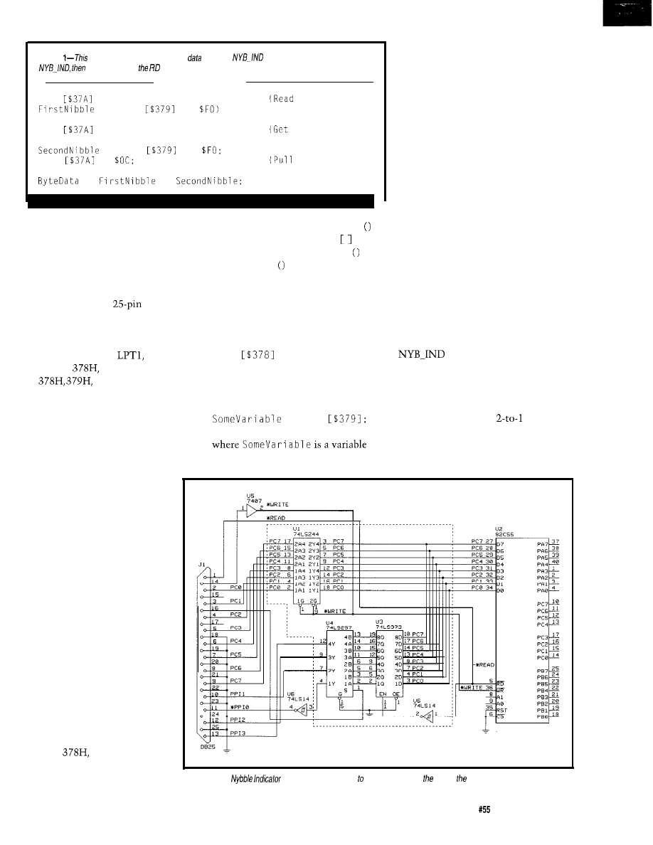
Listing
sample code reads in a byte of
using the
technique. If pin 16 is used as
pin
17 becomes
pin and bofh pins are negative logic.
Port
:= $00;
first nybblel
:= (Port
And
SHR 4;
Port
:= $08;
next nybblel
:= Port
And
Port
:=
RD high1
:=
Or
{Combine the nybblesi
series of computers have enabled
access) function was included as well!
bidirectional S-bit data transfer.
Recently, a DMA (direct memory
However, we will restrict our-
selves to the “original” parallel port,
which consists of a
D connector
(for pin assignments, see Table 1). Each
port has three addresses associated
with it in the I/O map of the PC. The
first parallel port, or
has a base
address of
so its addresses would
be
and 37AH. Each
address allows us to read or write
certain data to the parallel port to
control the logic state of each pin.
out
p o
r t b
functions in C enable the
direct manipulation of the parallel port
Features such as OUT and I N P
through these addresses.
instructions in BASIC, P o r t arrays
in Turbo Pascal, and i n
p o
r t b
and
Due to the design of the standard
parallel port, certain pins have nega-
tive logic while others use positive
logic. Port 379H involves
inversion of certain bits while
port 37AH does not when used
for input. As noted, we use port
378H to output 8 bits, port
379H to input up to 5 bits, and
port 37AH to input or output up
to 5 bits.
For faster access and greater
flexibility, software should
directly access these parallel
ports through the three ad-
dresses associated with it. As
used in the PC, parallel port 1
has address 378H for writing a
byte of data to output to the
parallel port pins, address 37AH
enables writing control signals,
and address 379H gives input
signals from a device. Therefore,
to output a byte of data, the
program writes a character to
address
and input may be
done at address 379H and
For example, to write the hex
value 27 to port 378H in Turbo Pascal,
we can write:
Port
:= $27;
Thus, to read data, we use the state-
ment:
= Port
capable of storing a byte of data
THE NYBBLE INDICATOR
APPROACH
Assume for a moment that we are
exchanging data between two comput-
ers using the parallel port. The
receiving computer needs to read data
from the parallel port, but can only do
so five bits at a time. This is an
inconvenient quantity, so we will just
use four of these bits for a nybble of
data.
Typically, when you manipulate
nybbles with software, you designate
one pin of the port to act as a nybble
indicator. The sending program is
responsible for splitting the data into
two nybbles and transfers it via four of
the five input pins on the parallel
interface.
One example of such a software
transfer may be seen in the code
segment in Listing 1. If the sending
party is a piece of software, then the
receiving program indicates with the
pin which nybble is to be
sent.
IN HARDWARE
If instead hardware is used to
transmit data, a quad
multi-
plexer solves the problem. Figure 1
shows the schematic connecting the
device to a standard parallel interface.
37AH.
Figure l-/n fhe
approach, a bit is used designate whether high or low nybble is being transferred.
Circuit
Cellar INK
Issue
February 1995
3 1
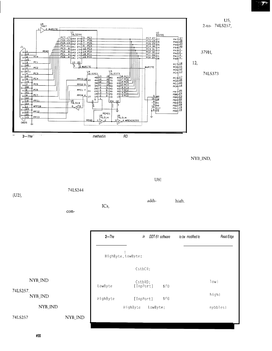
Figure
Read Edge approach differs from the previous
its use of the
line.
In our example, the nybble indicator
uses pin 16, which corresponds to bit 2
on port address 37AH.
Looking at the original DDT-5
1,
the data bus consists of pins 2-9 on the
parallel-port connector-it became
bidirectional through hardware
modifications. If the port is left
unmodified, we have to add a
which is used to isolate the data
bus of the 8255 from the parallel port.
THE READ EDGE APPROACH
Now,
let’s take a look at what we
did. For reasons that will be apparent
later, we will call this the Read Edge
method.
Figure 2 shows the schematic
with the new circuitry. We use a pair
of Schmitt-triggered inverters (U7,
to clean up the READ line. The
difference between the methods hinges
primarily in the use of the READ
signal. Here, together with the
low. This causes
a
quad
1
to
output the low byte to
the input portion of the
parallel port. (Again, we
are using bits 7, 6, 5, 4 of
port
which
correspond to pins 11, 10,
13 on the parallel
port.) The signal causes
U4, a
latch, to
pass data through to U5.
On receiving the
READ8255 signal, the
8255 places the data on
the bus, which connects
to U4. Since U4 is a
transparent latch, data
passes through it when
LE, which is connected to
the READ1 signal, is
high. This allows the data
to appear at the input of
U5, which selects the
lower four bits of the byte and outputs
this nybble. The READ signal, which
acts like the
goes to the
-A/B input of the multiplexer to
determine which nybble to place on
the input pins. In this case, it is low
for the lower nybble and high for the
higher nybble. These nybbles are
stored in the PC.
The software then pulls the READ
line
The LE on U4 then goes low
U2 is required as the DO-D7 pins on
tional
as shown in the figure, it is
the standard parallel port are
as the first Schmitt-triggered inverter
also used as the nybble indicator.
(U7) reverses the logic level of the
stantly outputting data to the data bus,
When the software needs to read a
which causes problems during an
signal. The falling edge of this signal
byte of data, it pulls the READ line
latches the output from the 8255.
input operation. Pins 11, 10, 12, and
13
are now used for input to the PC,
which correspond to bits 7, 6, 5, and 4
Listing
READ8255 routine the
has
work with the
on port address 379H.
hardware.
The dotted area in Figure 1 shows
the change to the original circuit. In
Function 8255 Byte:
this approach, the sequence of reading
Var
Byte:
a byte begins by setting the READ line
Beqin
high. To initiate a read operation, the
Port [CTLPortl :=
DDT-51 port values)
line changes to low., The software then
Port [CTLPortl := Cread:
pulls the
(active) high and
reads the first nybble from the
Port [CTLPortl :=
Pull RD
:= (Port
And
SHR 4
It then saves the nybble and
pulls the
low to read in the
Port [CTLPortl := Cnull;
Pull RD
next nybble. The read operation ends
:= Port
And
by setting the
and READ to
Read8255 :=
Or
Combine
high again. The -A/B pin of the
is connected to the
End:
pin on the parallel port.
32
Issue
February 1995
Circuit Cellar INK
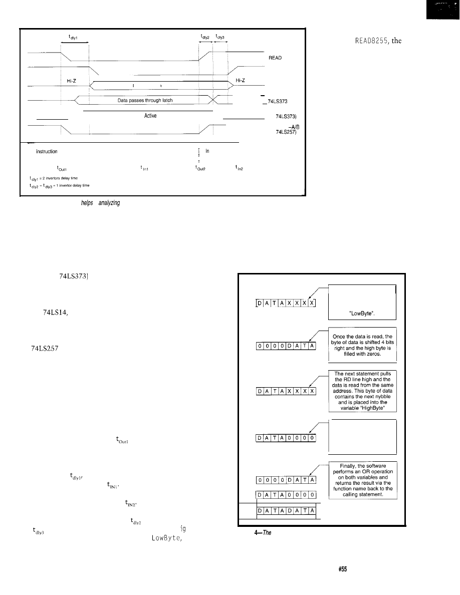
READ8255
Data
available
Data from
8255
Data latched
Data of
at output
Latch
I n a c t i v e
Latch
READ1 (to LE
of
Out
In instruction reads first nybble
Out instruction
instruction
causes READ
causes READ
reads in next
to go low
to go high
nybble
READ
(to
of
but we have demon-
strated that it does
The inverter delays are on the
work. Incorporating the
order of 10 ns using standard LS logic.
circuitry into a PLD
may lessen some of the
An I N instruction takes hundreds of
layout problems.
nanoseconds to execute for a PC. Some
of you may frown at using delays to
achieve our objectives,
Depending on the state of
the READ signal, the software either
shifts the nybble four bits to the right
or no shifting is performed at all.
As you can see in Listing 2, the
first nybble read represents the low
Since each read opera-
tion at address 379H yields
a byte of data, the software
ignores any unused bits in
the byte of data and zeros
them before storing them
into the variables. From
Table 1, we see that the four
input pins lie in the upper
four bits of the byte.
Figure 3-A timing diagram
in
the Read Edge approach for any possible delay problems.
When a statement calls
the
function
READ line on the parallel
port goes active (low). This
causes the hardware to
respond with the lower
nybble at the input pins.
The software then reads the
nybble from the input pin
through the address 379H.
After the rising edge of the
READ8255 signal, the 8255 releases
the data bus to a high-impedance state
at the same time or before U4 is able
to latch the data. The second inverter
(U8) delays the READ8255 signal so
that U4 (the
has time to
latch the data.
Latching is done before the
READ1 signal propagates through the
second
which pulls the
READS255 line at the 8255 high.
When this happens, the output from
the 8255 floats. Looking now at U5,
the
multiplexer, the high
READ signal outputs the high byte of
the data. The software reads the
nybble and then combines them to
form the final byte. Figure 3 shows the
timing diagram for the read operation.
TIMING ANALYSIS
Let us
analyze the timing of the
signals to see the potential and limits
of this approach. Look at time
in
Figure 3. After the CPU brings the
READ line low, an I N instruction
reads in the first nybble. Because of the
timing delay of
the first nybble
must be ready to be read by
However, the read for the second
nybble always finds data ready at
Now, if the CPU wants to do a
write to the 8255 instead, the time
and
causes the 8255 to change
from a READ state that is much
slower.
THE SOFTWARE
So far, we have been
talking about the
hardware that converts
bytes into nybbles for
the PC parallel port.
However, the approach
of reading such a byte of
data also requires the
use of software to
generate the necessary
read signal and assemble
the two nybbles into a
byte.
In the DDT-5 1
project, we modified the
READ8255 function to
achieve this. Listing 2
shows the code samples
written in Turbo Pascal.
Note that there are two
variables H
h By t e and
both of the
data type BYTE.
Software executes a read
to
obtain a byte of data
from address 379H and
places it into variable
Software next fills the low
byte with zeros.
+
Figure
nybble manipulations needed to recover a byte of data when
on/y four bits of the data are transferred at a time are readily coded in most
languages.
Circuit Cellar INK
Issue
February 1995
33
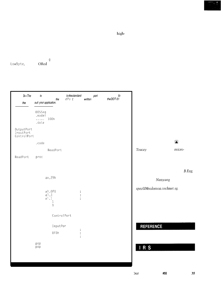
byte. The software shifts this nybble
four bits to the right and fills the upper
nybble with zeros. It then pulls the
READ line high to read the next
nybble. The second nybble, which
represents the high byte, need not be
shifted at all since it is already in its
correct position. The lower nybble is
then filled with zeros.
Once the software stores the two
nybbles in the variables
H i h Byte
and
they are
together. The
last statement in the function then
places the result into the function
name, which returns the value to the
calling statement. Figure 4 illustrates
the process of the software performing
the read and assembling the two
nybbles.
ASSEMBLY LANGUAGE
Writing the code using a
level language to read the nybbles and
assembling it to form the final byte of
data may be too slow for certain
applications. To solve this, you can
use an optimizing compiler to produce
a faster routine or simply write the
READ8255
function in assembly
language to begin with.
We have converted the
READ8255
function to C and used Borland C++
3.1
to
compile the program. By turning
on the speed-optimization option, the
Listing
routines
read and write data
PC parallel
are generic enough be
useful for most applications. However, Re a
r routine is
specifically for
project.
Modify code fo
small
stack
equ
378h
equ
379h
equ
37Ah
public
push dx
push cx
mov
dx,ControlPort
mov
out
dx,ax
mov
dx,InputPort
in
al,dx
and
shr
shr
shr al,
shr al,
mov ch, al
mov
dx,
mov
ax, 08h
out
dx, ax
mov
dx,
in
al, dx
and al,
or
al, ch
cx
dx
ret
endp
end
: assert RD line low
; read the nybble
zero the lower nybble
faster to do 4 * 1
bit shifts
; save nybble
; pull read line high
read upper nybble
zero lower nybble
merge nybbles into bytes
compiler was able to generate a fast
routine for the read operation that was
almost as fast as one we hand-opti-
mized in assembler.
Turbo Pascal, however, produces a
final assembly listing with some slight
overhead in the code. The overhead
may be avoided by simply writing the
assembly version. We provide a sample
of the assembly version of our
READ8255
in Listing 3.
CONCLUSIONS
Although the Read Edge approach
allows the software to read a byte of
data using a standard parallel port with
a single READ signal, it cannot be
used on two PCs without this hard-
ware between them.
But, this method is one of the
many ways to read data using a
parallel port. Its main advantage lies in
the use of the READ signal to differen-
tiate the nybbles in the data byte. This
saves one pin on the parallel port
which may be used for other purposes
such as a control line for the attached
device. Furthermore, this technique
reduces the complexity of the software
as less coding is required.
Lee
specializes
in
systems in the Department of Elec-
tronics, Computer, and Communica-
tions Engineering at the Singapore
Polytechnic. He worked for IBM
Singapore for 8 years and has a
from Singapore University and a
M.Eng. from
Technology
University. He may be reached at
Kok-Leong Ong recently finished his
studies at the Singapore Polytechnic
where, together with two other
students, he worked on a final year
project entitled “8051 Emulator.”
Ciarcia, Steve. “Why Microcon-
trollers?” BYTE, Aug.-Sept., 1988.
410
Very Useful
411 Moderately Useful
412 Not Useful
Cellar INK
Issue
February 1995
operated
Power
David Prutchi
Supplies
Selecting the Right Battery and
Supply for Your Application
hen designing
or isolated
‘instruments, one of the
main concerns is often the power
source for the system. These applica-
tions usually can’t rely on a
operated power supply and thus a
battery-operated source becomes
necessary.
A number of battery, charger, and
DC/DC technologies are currently
available. However, careful consider-
ation of many factors is imperative in
selecting the right kind of battery for a
given application.
On one hand, the electrical
attributes of the battery constitute
the design constraints of the power
supply, along with the load character-
istics, power demand, and required
operation time. On the other hand,
physical and safety conditions restrict
the number of technologies that
conform to the electrical specifica-
tions. Finally, battery price and
maintenance costs narrow the remain-
ing alternatives.
In addition, the mission objectives
for the instrument must be carefully
analyzed to determine whether a
nonrechargeable battery (also called a
primary battery)
or a rechargeable
battery (secondary battery] should be
used.
Once a battery matches the
required specifications and is selected,
an appropriate DC/DC converter must
be designed to supply the various
subsystems of the instrument with the
voltage levels each requires. If re-
chargeable batteries are used, charging
and maintenance circuitry must be
designed.
This article discusses proper
battery system design for self-con-
tained microcomputer applications.
Battery selection considerations as
well as power-conversion design is also
addressed.
PRIMARY BATTERIES
Primary batteries convert chemi-
cal energy irreversibly into electrical
energy. As such, they are not meant to
be recharged. The main advantages of
these batteries are their high-energy
density, good shelf life, wide availabil-
ity, and maintenance-free operation
Standard zinc-carbon
cells-have
a thin, solid zinc (Zn) casing for an
anode. This is surrounded by a moist
cake of manganese dioxide powder
and an electrolyte solution of
granulated carbon and zinc chloride
blended together with ammo-
nia (NH,). A carbon-rod electrode is
introduced into the solution.
Energy for the discharge current is
obtained by turning zinc into zinc
diammino chloride
and
by reducing the manganese dioxide to
manganese oxyhydroxide
through the reaction:
Zn
Zn
+ 2MnOOH
(1.5 V)
Standard zinc-carbon cells have not
changed all that much since they were
introduced over 100 years ago by
Their main advantage is
that they are the cheapest batteries
that can be bought. Their main
disadvantage is that their voltage drops
and their internal impedance increases
steadily as the battery is used. More-
over, their capacity is severely reduced
when used at high currents.
36
Issue
February 1995
Circuit Cellar INK
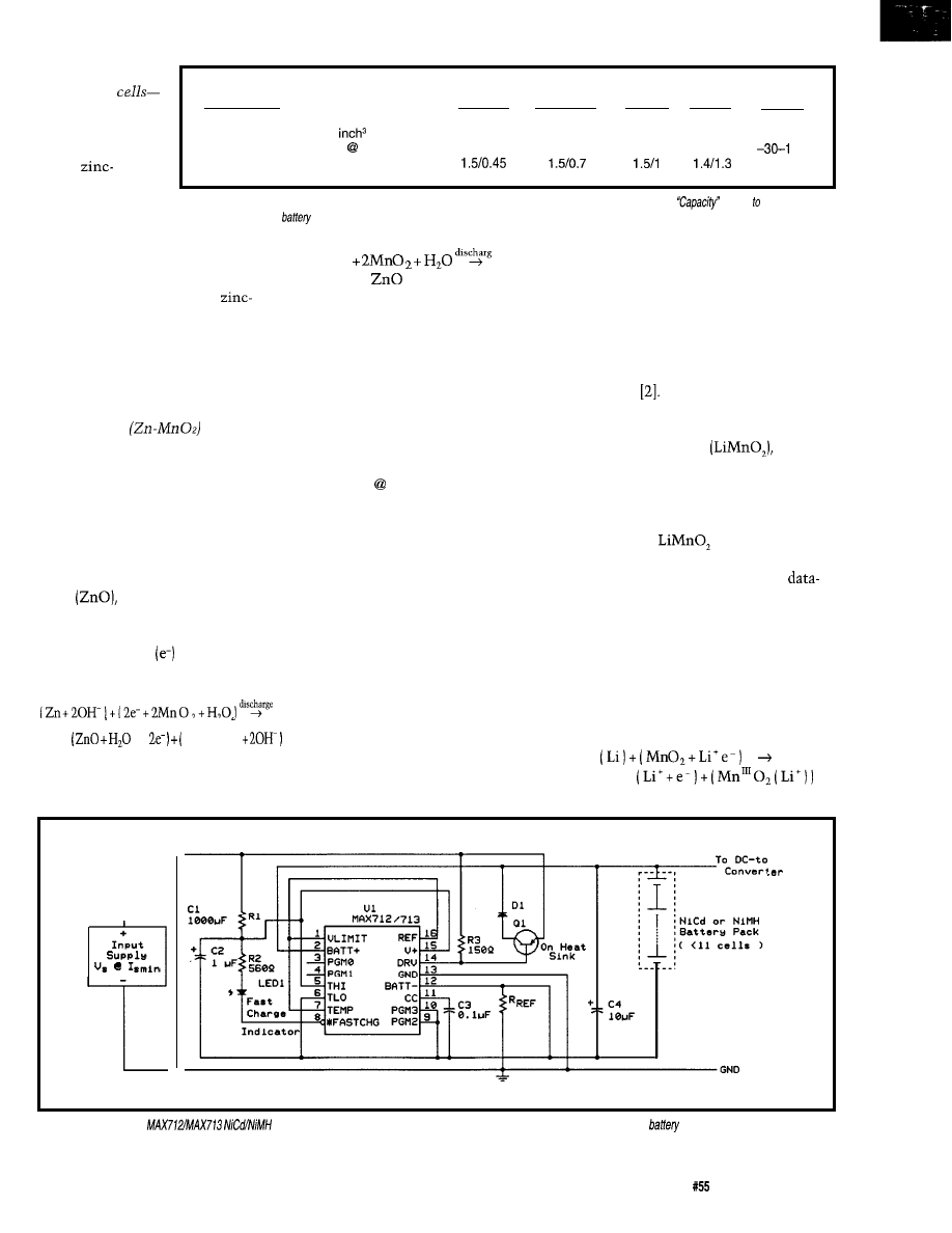
Heavy-duty
zinc-carbon
are improved
Leclanche cells
which incorporate
higher
chloride content
and modified
design to cope
with higher gas
Zinc-Carbon Zinc-Carbon
Lithium
Characteristic
Standard
Heavy Duty Alkaline
Mercury (various)
Capacity (Ah max., largest available)
3
5
20
1
8
Energy Density (Wh per
max.)
2
2.5
3.5
7
8
Temperature Range (0°C 85% capacity)
1 o-55
5-65
2-70
3-75
00
Cell Voltage (V, full/empty)
413.8
Table l--Typical primary batteries vary in their charge capacity, current-supplying capability, and cell voltages.
refers the
largest
standard commercial
that is wide/y available.
generation during operation. Although
their energy density is only slightly
higher than that of standard
carbon cells, their capacity is not as
strongly affected by high-current
operation. In addition, the tolerance of
heavy-duty cells to temperature is
somewhat better than that of standard
cells.
Alkaline
cells-are the
most widely used household batteries
today. Inside them, zinc is used as the
anode material and manganese dioxide
as the cathode. Electrochemical
activity takes place through a potas-
sium hydroxide electrolyte. The
energy-producing reaction involves
oxidizing the zinc anode to form zinc
oxide
while reducing the
manganese dioxide to manganese
oxyhydroxide. This reaction, which
supplies electrons
for the discharge
current, can be expressed as:
Zn
+ 2MnOOH
(1.6 V)
Because of their low internal resis-
tance, low currents can be drawn from
alkaline cells for very long periods of
time, and they have a moderate energy
density. As with zinc and carbon cells,
their main disadvantage is a sloping
discharge curve. In addition, the
largest serial-connection battery packs
can achieve a maximum current of
about
1
A 4 Ah using D-size cells.
In general, alkaline batteries are
very inexpensive, widely available, and
have relatively good shelf life. These
characteristics make them the favorite
choice for household battery-powered
equipment, but their degraded perfor-
mance at low and high temperatures
should be of real concern to designers
of equipment exposed to harsh
environments.
Lithium
cells-are one of the
newest commercial primary cells
their wide temperature range of
operation, extraordinary shelf life, and
very good discharge voltage regulation.
One large disadvantage of lithium cells
is that they still present a safety
hazard because of their extremely high
energy density and the toxicity of their
contents
One of the most common lithium-
cell chemistries is based on lithium
manganese dioxide
which
comes in a variety of packages.
Because of their long shelf life, these
batteries are commonly used as
memory backup supplies. However,
high-power
cells are used
today as the main power source for
intelligent cameras, flashlights,
acquisition packages, test and measur-
ing instruments, and so on.
Similar to alkaline batteries, the
energy-producing reaction involves
metallic lithium (Li) and manganese
dioxide. The exact reaction path is still
unknown, but it has been suggested as:
anode
cathode-
t
2MnOOH
exhibiting very high energy density.
anode
cathode
Although there are various lithium-
discharge
based chemistries available, the
which is simplified to:
common advantages to these cells are
r
Input
-DC
Figure l--Maxim’s new
battery fast-charge controllers can be the basis of a low-cost,
low-parts-count
charger circuit. S ee the article for
guidelines on how to pick values for the unspecified components.
Circuit Cellar INK Issue
February 1995
37
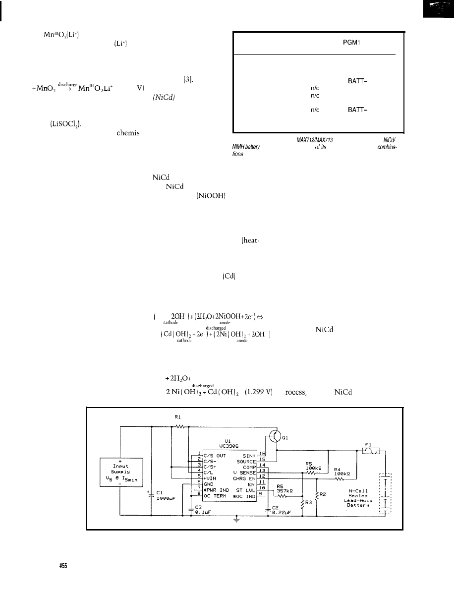
where
represents the
introduction of a lithium ion
into
the manganese dioxide crystal lattice.
This last equation is simplified for the
overall cell reaction to:
Li
(3.0
Another kind of lithium cell in
use today is based on lithium thionyl
chloride
This cell is replac-
ing older alkaline and lithium
tries in military instruments.
Other primary batteries-with
different chemistries are commercially
available. However, unless a critical
design constraint demands their use,
the best idea is to select the most
widely available batteries and to avoid
hard-to-get types. Two battery chemis-
tries that should nevertheless be
mentioned because of their extensive
use in miniaturized instruments are:
l
silver oxide cells-These batteries
are typically used in watches and
cameras. They have very flat
discharge characteristics, but have a
shorter shelf life than lithium
batteries.
l
zinc-air batteries-These generate
the life of the product
they empower and
provide an effective
method of storing
energy for cordless
operation
Nickel-cadmium
cells-take
advantage of a revers-
ible electrochemical
reaction in which the
active electrode
materials change in
oxidation state
Number of Cells PGMO Connection
Connection
(n)
(Pin 3)
(Pin 4)
1
V+ (pin 15)
2
V+ (pin 15)
3
V+ (pin 15)
4
V+ (pin 15)
5
6
7
n/c
8
9
REF (pin 16)
10
REF (pin 16)
V+ (pin 15)
n/c
REF (pin 16)
(pin 12)
V+ (pin 15)
n/c
REF (pin 16)
(pin 12)
V+ (pin 15)
n/c
Table 2-“Programming” the
to charge an n-celled
is done by connecting two
input
pins in different
without any physical
deterioration. This property gives
cells a relatively long life.
cells use a nickel
oxyhydroxide
anode, a
cadmium (Cd) metal cathode, and a
potassium hydroxide (KOH) electro-
lyte. During the charge cycle, the
anode is reduced to nickel hydroxide
(Ni( OH),) in an endothermic
absorbing) reaction. During discharge,
the anode returns to its primary state,
while the cadmium metal is oxidized
to cadmium hydroxide
OH),),
releasing electrons to the load. These
reactions can be expressed as:
electricity through a chemical
charged
reaction which uses the oxygen in
Cd +
the air. They have extremely high
power density and, for this reason,
have started to gain ground as a
replacement for mercury batteries in
which is simplified to:
hearing aids, medical telemetry
equipment, and pagers.
charged
Cd
2NiOOHo
Table 1 offers a summary of the
primary batteries
discussed.
SECONDARY
BATTERIES
Secondary
batteries are
designed around
chemical reac-
tions with
electrochemical
reversibility,
which makes
them recharge-
able. These
batteries offer
cost savings over
The endothermal characteristic of
the charging reaction offsets the heat
produced by the inefficiency of the
charging process, resulting in an
almost constant battery temperature
during the charge cycle. However, on
completion of this cycle, cell over-
charge leads to a sharp increase in
battery temperature. A sensor moni-
toring this temperature change may
use this as a signal to terminate
battery charging. This temperature
shift is often used in the control of fast
charging. High charging current must
be reduced immediately at the mo-
ment of temperature rise to prevent
the development of excessive gas
pressure.
When
cells move into the
overcharge region, the voltage peaks
and then begins a clear-cut decline.
Detection of the resulting negative
slope of the voltage curve can also be
used to terminate charging. Depending
on the design and manufacture
p
modern
cells can be
Figure 2-A UC3906 is at the core of fhe design of a sealed-lead-acid battery charger which implements an optimal charging and maintenance
algorithm. Again, see the article for component-value selection guidelines.
38
Issue
February 1995
Circuit Cellar INK
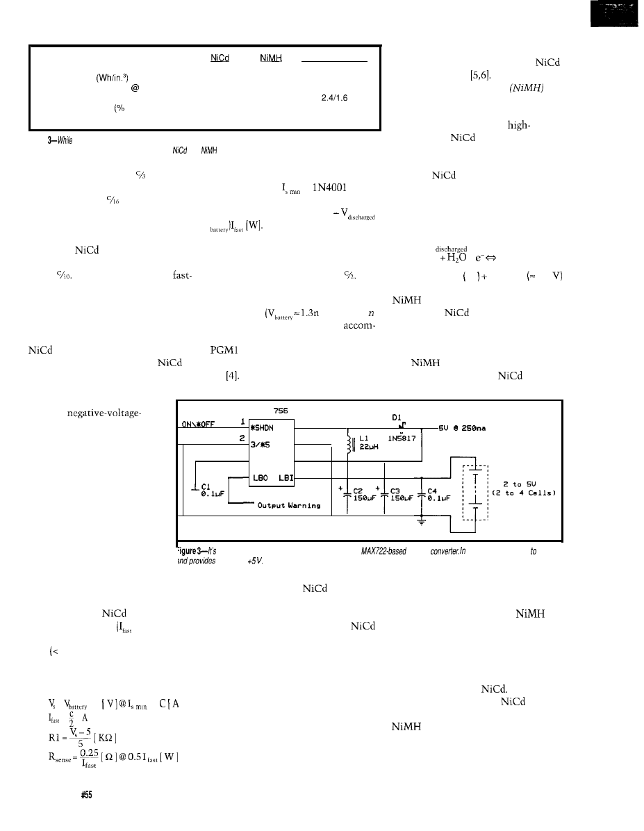
Sealed Lead-Acid
Capacity (Ah max., largest available)
5
8
25
Energy Density
1.2
1.8
1
Temperature Range (“C, 85% capacity)
-15 to 40
-20 to 45
-50 to 50
Cell Voltage (V, full/empty)
1.3511
1.411.1
Self-Discharge Rate
per month)
25
30
6
Number of Full Cycles
800
500
200 to 2000
Table
sealed-lead-acid batteries might appear to be the device of choice when selecting
a secondary
battery, they are much larger and heavier than
and
batteries.
fast-charged at rates
from (where C
Note that Dl’s minimum current
is the rated battery capacity) up to 4C.
handling equals
(a
is
After this point, a
trickle-charging
usually suitable) and Q l’s minimum
rate should be used to maintain full
power dissipation equals (V,
battery capacity during idling condi-
tions.
Nickel-metal hydride
cells-are starting to appear in the
market. These batteries have similar
characteristics to those of
performance
types, but have as
much as 30% higher energy density
(almost twice the energy density of
standard
cells). Their operational
principle lies on the ability of certain
metallic alloys to reversibly absorb
hydrogen atoms into the metallic
structure of the alloy:
Older
cells, on the other
hand, do not accept high charging rates
above
It should be noted that
charging rate selection is critical
because rates higher than those
specified for a cell cause electrolyte
seal leakage and gas-bubble formation.
plished by strapping lines PGMO and
Connecting lines PGM2 and
according to Table 2. For design
PGM3 to BATT program the MAX712
to timeout in a period of 264 minutes
and to use a fast-charge rate of
In
specifics of the MAX712 and MAX713,
addition, the MAX712 must be told
how many cells there are in the
see
battery pack
[V] where
is the number of cells). This is
alloy
+
charged
alloy H OH-
1.2
Figure 1 presents the circuit of a
battery-pack charger. The heart
of the circuit is Maxim’s new
battery fast-charge controller IC, the
MAX713. It is capable of
charging up to 16 series cells
and uses
slope detection and an internal
timer to switch automatically
from fast to trickle charging.
batteries are similar in con-
used to form the metal hydride
struction to
batteries, except
that proprietary alloy formulations are
cathode instead of cadmium.
charging methods are
similar to those used on
cells.
MAX
8
L X
.
Under a different circuit
configuration, the MAX713
can also use temperature
sensing to terminate fast
charging. In addition, the load
can be powered while charging
the batteries without affecting
the controller’s response. Of
course, the input supply
should be capable of supplying
enough current for both battery
charging and powering the load.
7
G N D
3 6
REF
OUT
4 5
T
Low Battery
possible to achieve 87% efficiency with this
DC-DC
this case, it runs on 2 4 cells
regulated
their performance and useful life.
The discharge of
batteries
When the load is connected to a
battery, the cell voltage should not be
should be monitored to maximize
allowed to drop under 1.1 V as this
may result in permanent plate and/or
electrolyte damage. Monitoring can be
accomplished through a simple
comparator circuit that disconnects
the load at the right time.
must take into account that
However, the selection of charging
batteries heat up during charging.
Although they exhibit a sharp tem-
perature increase on overcharge, the
control and termination parameters
negative slope to the voltage curve at
the end of charging is much less
marked than that of
capacity will fall. For an in-depth
review of how to charge and use
batteries, refer to
For a simple
charger with a
fast-charging current
[A]) of less
than 0.6 A and a battery of less than 11
cells
15
V), unregulated DC input
supply can be selected for the circuit of
Figure 1 using the following:
=
+ 3
= I
= I 1
40
Issue
February 1995
Circuit Cellar INK
Further, the battery should be
allowed to completely charge and
discharge (down to 1.1 V per cell) at
least 60% of the time or the battery’s
The circuit charging
batteries can also be used to charge
batteries by replacing the
MAX713 with a MAX712, which
takes into consideration these differ-
ences.
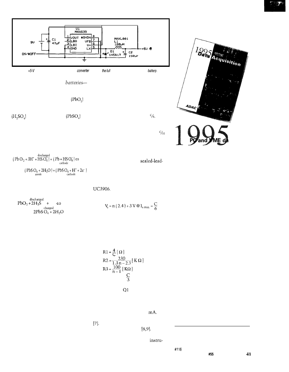
FREE
7 5 m A
Figure
4-A
output,
94% efficiency DC-DC
exploits
capacity of a
9-V
alkaline
Sealed lead-acid (SLA)
share the same chemistry of automo-
tive lead-acid batteries. During the
discharge cycle, a lead dioxide
anode and a metallic lead (Pb) cathode
react with the sulfuric acid electrolyte
to form lead sulfate
and water. The electrons are given to
the discharge circuit.
During the recharge cycle, the
same reactions are reversed. These
reactions can be expressed as:
anode
charged
which can be simplified for the overall
cell reaction as:
0, Pb
(2.041 V )
SLA batteries differ from
“flooded” lead-acid batteries in that a
minimum amount of electrolyte is
used. Their maintenance-free opera-
tion is the result of a gas-recombina-
tion technique in which the oxygen
and hydrogen generated within the cell
are recombined to maintain the
amount of water needed for operation.
SLA cells have a very low internal
resistance, which allows them to
source a high current. Their primary
advantage is their cost and the high
number of cycles they can withstand.
They have good storage-capacity
retention and discharge-voltage
regulation. In addition, the tempera-
ture range for their operation exceeds
that of most other secondary batteries.
The main disadvantage of SLA cells is
their relatively low energy density,
which makes SLA batteries much
heavier and voluminous than other
secondary batteries of the same
capacity.
During the charge cycle, a SLA
battery is typically brought up to
overcharge at about 2.4 V per cell
under a bulk charging rate of When
the final charging voltage is reached,
charging current through the battery is
slowly dropped to a trickle rate of
to maintain a float voltage of 2.25-2.3
V per cell. Without this trickle charge,
stored or idling SLA cells lose a
considerable amount of their capacity.
Unitrode’s UC3906
acid battery-charger chip implements
an optimal charging algorithm for
these batteries. The circuit in Figure 2
is a typical application for the
The circuit is supplied with
unregulated DC at:
where n is the number of cells in the
battery and C is the nominal 20-h rate
capacity of the battery. A simplified
set of equations to select component
values for the circuit is:
Fuse rating= [A] slow- blow
Transistor should be chosen to
meet charging current and voltage
requirements, taking into consider-
ation that the output drive current of
the UC3906 is limited to 25
For
detailed design information, refer to
Specific applications using the
UC3906 can be found in
Other secondary batteries-are
used to power self-contained
Data Acquisition
Catalog
ta
acquisition catalog
from the inventors of
plug-in data acquisition.
Featuring new low-cost
A/D boards optimized
for Windows,
DSP Data Acquisition,
and the latest
Windows software.
Plus, informative
technical tips and
application notes.
Call for your free copy
l-800-648-6589
ADAC
American Data Acquisition Corporation
70 Tower Office Park, Woburn, MA 01801
p h o n e 6 1 7 - 9 3 5 - 3 2 0 0 f a x 6 1 7 - 9 3 8 - 6 5 5 3
Circuit Cellar INK Issue
February 1995
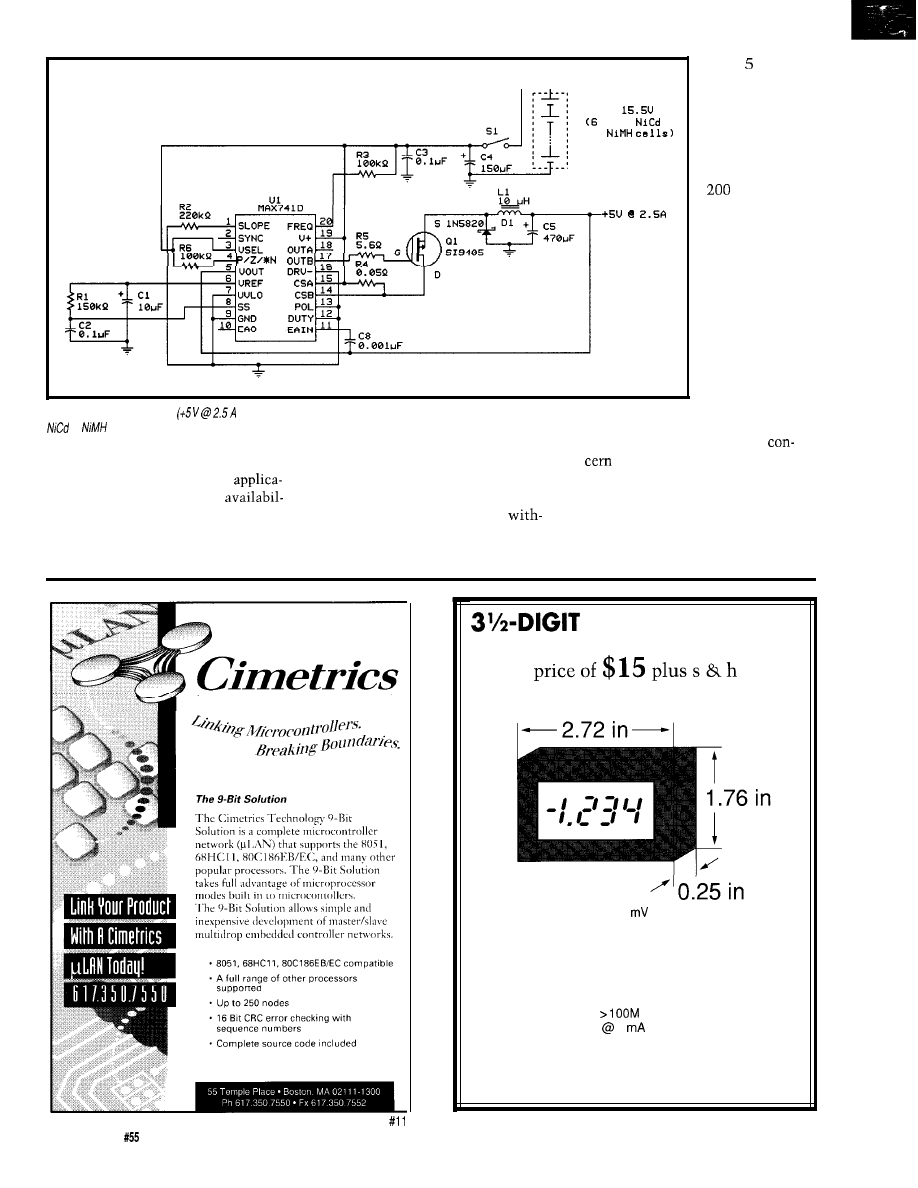
6 t o
t o 8
o r
Figure 5-A medium power
max.) DC-DC converter can be used to power a notebook-type microcomputer using a rechargeable
or
battery pack.
about years.
Once they are
loaded with a
liquid potassium
hydroxide elec-
trolyte, they can
be charged up to
times within
a two-year life
period. Although
they are expen-
sive, require
considerable
maintenance,
and have a rela-
tively limited
life, they are the
battery of choice
for applications
in which weight
and volume are
the main
ments. However, these are not cur-
*
Silver-Zinc cells
are usually used for
because of their attributes.
rently available for consumer
military and aerospace applications
They provide large energy density,
tions. Their cost and lack of
and are not common in commercial
excellent capacity retention, and
ity should deter the experimenter from
markets. These cells are kept
almost-flat discharge characteristics.
their use. Nevertheless, two other
out electrolyte until the day they are
.
Lithium-ion batteries
were only
technologies are worth mentioning:
put to use. Their dry shelf life is
recently introduced to the market.
T
E
C
H
N
O
L
O
G
Y
LCD PANEL METER
-Available now at an unheard of
N e w ! N o t s u r p l u s !
Specifications:
Maximum input: f199.9
additional ranges provided through
external resistor dividers
Display: 3%digit LCD, 0.5 in. figure height,
jumper-selectable decimal point
Conversion: Dual slope conversion, 2-3
readings per sec.
Input Impedance:
ohm
Power: 9-l 2 VDC
1
DC
Circuit Cellar, Inc.
4 Park Street, Suite
12, Vernon, CT 06066
Tel: (203) 875-2751
Fax: (203) 872-2204
42
Issue
February 1995
Circuit Cellar INK
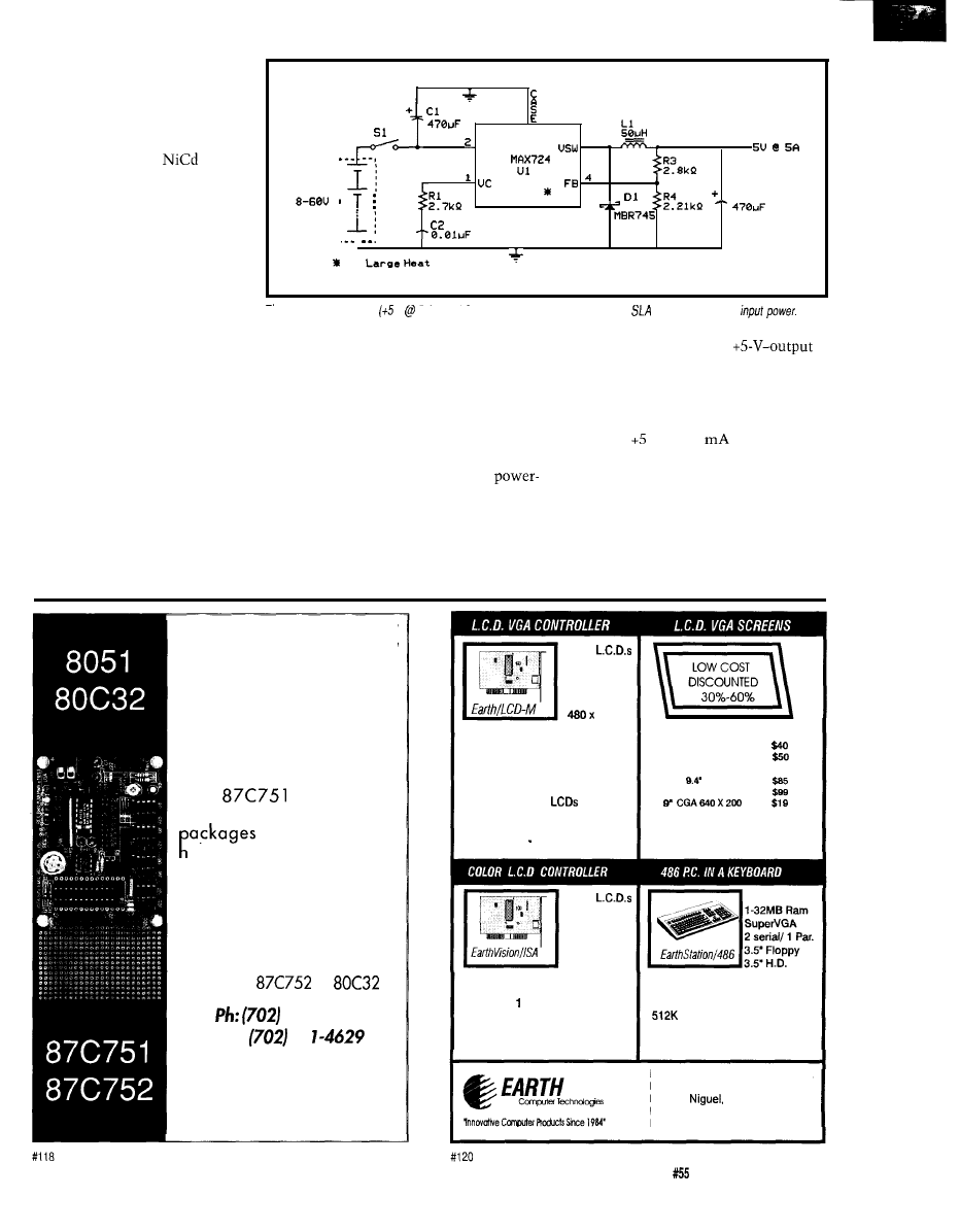
These rechargeable batteries,
with 3.6 V per cell, have
similar characteristics to those
of primary lithium batteries,
and feature about twice the
energy density of
cells.
These batteries are worthy of
special note particularly because
the first is often encountered in
government-issue equipment
and is of interest to the surplus
hunter, and the second has great
potential.
A summary of secondary
battery technology is in Table 3.
GND
UIN
3
T O - 3
_ _ c 3
__
O n
S i n k
DESIGN OF BATTERY-OPERATED
POWER SUPPLIES
Many battery-powered instru-
ments are designed to operate directly
from the battery without further
power transformation or regulation.
This design approach offers a low parts
count and a very high power effi-
ciency, but unfortunately is seldom a
viable option. Power conversion or
regulation is generally required.
Figure 6-A
high-power
V
5 A
max.)
DC-DC
converter uses high-capacity
batteries to provide
Whenever step-down regulation is
One of the simplest
DC-DC converters for battery-powered
applications is depicted in Figure 3. Up
to 87% efficiency can be obtained by
using this circuit. Maxim’s MAX756
delivers V at 250
from 2 to 4
cells and even includes an on-chip,
MOS, digitally controlled power
switch and a power-fail signal to warn
the microprocessor when the output
falls out of regulation.
required, three-terminal linear regula-
tors may be used to keep the circuit
cheap and small since they are widely
available, simple to use, and don’t
require support components, except for
decoupling capacitors. However, linear
regulators are seldom used in
conscious designs because they are less
efficient than modern switching
regulators. In addition, linear regula-
tors cannot step up or invert battery
voltages.
The 9-V “1604” batteries are
appealing to hand-held instrument
Use one of our embedded
controllers to save time and
money.
They are ideal for
developing products, test
fixtures and prototypes.
We offer a complete line of
c o n t r o l l e r b o a r d s a n d
software tools for the 8051
a n d
f a m i l i e s o f
microcontrollers. Complete
are available to
e l p y o u d e v e l o p y o u r
projects.
Features:
l
Breadboard area
l
Flexible I/O arrangement
l
Powerful controller
BASIC
for the
or
83 I-6302
Fax:
83
Iota Systems, Inc.
POB 8987
l
Incline Village,
NV
89452-8987
ISA 8
BIT
PC. COMPATIBLE
Mono
Supported:
640 x 480
640x200
320 x 200
128
WINDOWS DRIVERS
HARDWARE PANNING
RUNS VGA PROGRAMS
ON LOW RES
INCLUDES 10% OFF ANY
LCD PANEL DISCOUNT
LOW COST $149
Color
Supported:
Single Scan
Dual Scan
TFT
ISA 16 BIT VGA
WINDOWS ACCELERATOR
512K OR M RAM
CHIPS &TECH 65545
FASTEST LCD CHIP
LOW COST $299
MONO REFLECTIVE
VGA 9.4’ [IN A CASE!!]
VGA 7’
MONO BACKLIT
VGA
250 MS
VGA 9.4’ 150 MS
COLOR BACKLIT
VGA 9.4’ SNGL SCAN
$99
VGA 9.4” DUAL SCAN
CALL
VGA TFT 9.4”
CALL
33 Mhz 486SX
101 KEYBOARD FOOTPRINT
FULLY PC AT COMPATIBLE
ONE 16 BIT ISA SLOT
FLASH DRIVE AVAILABLE
ETHERNET DISKLESS FROM
$849 RETAIL!
Earth Computer Technologies, Inc.
P.O. Box 7089
Laguna
CA 92607
Phone: (714) 448-9368
Fax: (714) 448-9018
Circuit
Cellar
INK Issue
February 1995
43
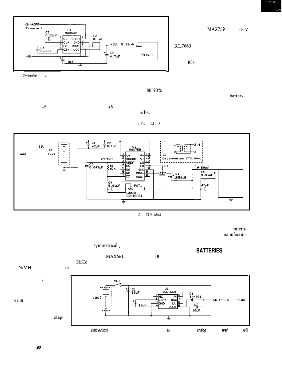
input. Symmetrical output is easily
obtained using the industry-standard
operating within the circuit
F l a s h
in Figure 9.
C l
Finally, full-function portable
_
power
such as Maxim’s MAX714,
‘715, and ‘716 chips, combine mul-
Figure
volts
power is supplied by dedicated DC-DC converters to program flash memory in such
instruments as palmtop computers and stand-alone data loggers.
tiple-voltage DC-DC regulators,
backup-battery switchover, and
microprocessor-supervisory functions
designers because they are small,
5 A with efficiencies in the
in a single package to simplify the
readily available, and easy to connect
range.
design and manufacturing of
to. A MAX639 provides a very elegant
Not all circuits in an application
powered, microcomputer-based
way of getting V out of one of these.
require V, and DC-DC converters
instruments.
Using a 9-V alkaline battery with the
are available to produce
voltages.
These are only a few examples of
circuit of Figure 4, more than 40%
For example, some flash-memory
the many possibilities available to the
extra battery life is possible using the
programming requires
V,
designer. Check data books and
flash memories. As shown in Figure 8,
0 to -24-V LCD-bias voltage can be
obtained using a
from a
4 t o
to 6
c e l l s
regulated
0 t o - 2 4 U
CONTRAST
C 6
LCD
LCD
Figure
8-Negative LCD contrast voltage can be generated using this DC-DC converter with to
MAX639 instead of a low-dropout
linear regulator!
For higher power requirements in
instruments which integrate a com-
plete microcomputer, high-efficiency
step-down switching regulators can be
used to convert the power of 6-8
or
cells in series to V. The
circuit in Figure 5 reaches
93 % efficiency providing
a maximum current of up
to 2.5 A. If you have higher
current requirements, the
V obtained from
sealed-lead-acid batteries
can be used with a
MAX724 high-power
down DC-DC converter as
shown in Figure 6. This
power IC can supply up to
display contrast controls require
voltages down to -24 V, and bipolar
A/D and D/A converters require
Dower.
application sheets provided by
power DC-DC converter
ers for more information.
The circuit in Figure 7 makes use
BACK-UP
of the
a 5-12-V input
Back-up batteries are normally
DC converter, which produces a
used to maintain volatile memory and
regulated +12-V output to program
real-time clock devices which operate
+Ub
1.5 to
c 2
to
C A P -
0
Figure
9-This
creates a symmetrical voltage about ground power dual-supply
circuits, as
as bipolar
and D/A converfers.
44
Issue February 1995
Circuit Cellar
INK
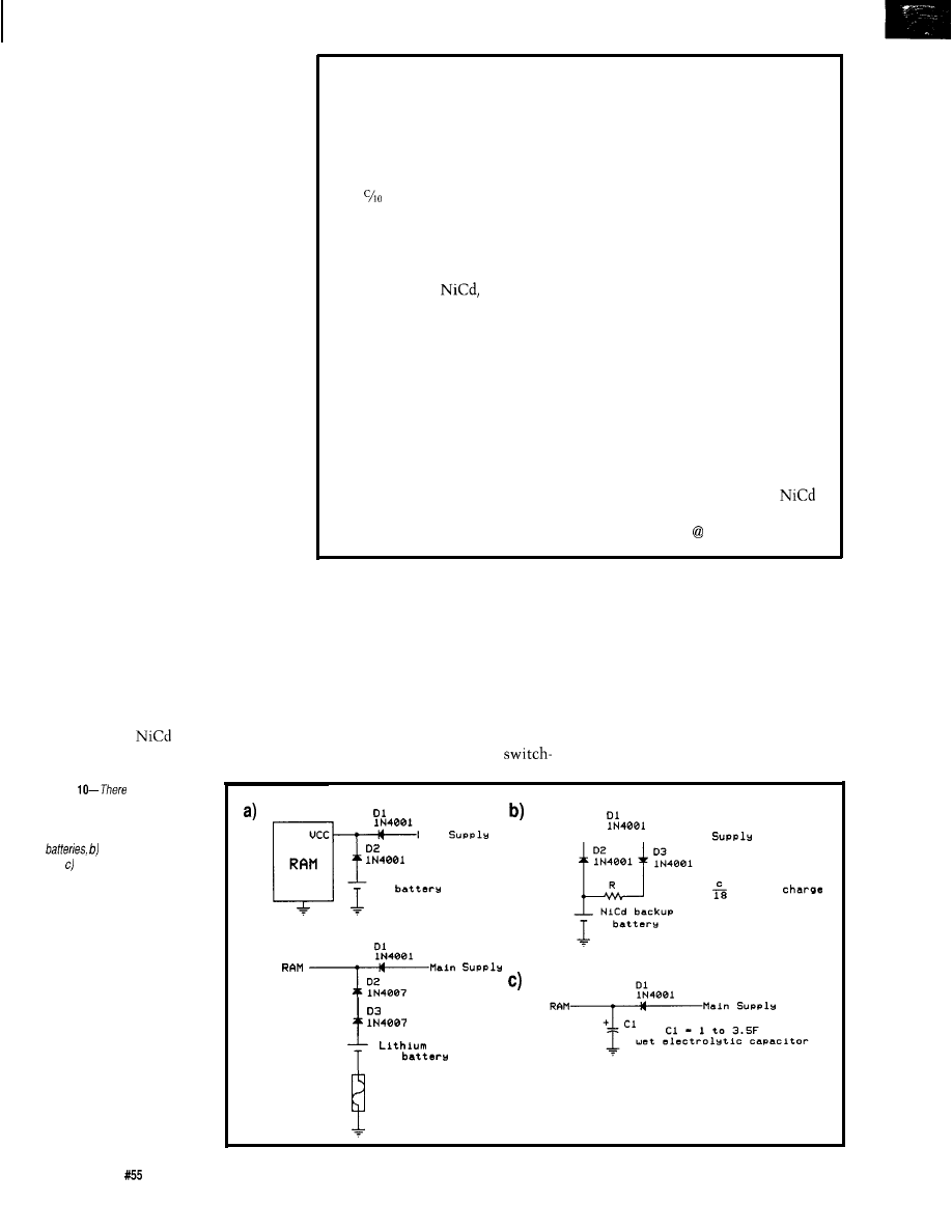
after the main power has been,
willingly or accidentally, turned off.
Figure 10 shows three possible meth-
ods the designer can choose to keep a
device powered.
The first makes use of a primary
battery, which must be isolated using
a diode to prevent charging the battery
by the main supply. The second option
involves using a rechargeable battery,
which is trickle charged by the main
power supply. The last option uses a
very large (capacitance-wise) capacitor
as the back-up energy storage device.
With the recent advent of the
small 5.5VDC capacitors with super
high capacitance (up to 3.5 F), the
latter option becomes the most
convenient. They are highly reliable,
compact, and have superior stability
over repeated charge and discharge
cycles. Rechargeable batteries work in
this application very much like a large
capacitor, but a simple trickle-charge
circuit can hardly take advantage of
the battery’s full life, which leads to
relatively low reliability.
The use of primary batteries is the
most popular today, not only for the
simplicity of the design, but also
because they permit a much larger
period of data retention. When used
with a modern micropower CMOS
RAM, an alkaline or lithium battery
maintains data for a period which
approaches its shelf life, while a
capacitor or a
battery requires
periodic charging.
Figure
are several
backup-power options for volatile
memories and CMOS micropro-
cessors including a) primary
secondary batteries,
and large energy-storage
capacitor.
Battery Glossary
Bulk Charging Rate-current flow through a secondary battery forced by
the charger during the fast-charging part of the cycle.
Capacity (C)-the ability of a fully charged battery to supply current over a
certain time period. Capacity is measured in ampere-hours [Ah]. Capac-
ity, as marked on batteries, is usually defined for a battery-discharge rate
of at a constant 20°C temperature. Capacity changes drastically as a
function of discharge rate, temperature, and state of charge.
Discharge Voltage Regulation-stability of the voltage across the battery as
a function of discharge. For example, zinc-carbon, alkaline, and lead-acid
batteries slowly decrease in voltage as they discharge. There are others,
however, like
mercury, and lithium that maintain an almost
constant operating voltage over the entire discharge cycle, with a sudden
drop at the end.
Float Voltage-voltage at which a rechargeable battery cell may be held
indefinitely without damage.
Overcharge Voltage-voltage which must be reached during the charge
cycle of a secondary battery to achieve full capacity.
Primary and Secondary Batteries-Primary batteries are used only once
while a secondary battery is a storage device that can be discharged and
recharged to its full capacity many times.
Self-Discharge-is the rate at which an idling (or stored) battery loses
capacity as a function of temperature. For example, an unattended
battery loses all of its charge in about 3 months, while a solid-state
lithium battery has a shelf life of more than 20 years 70°C.
Most primary batteries can be
over can be implemented using a
used for backup. However, if the
application demands the use of
lithium technology, it is better to
isolate the battery from charging
currents using two diodes in series as
well as a low-current fuse on the
ground side. If noise-free back-up
battery switching is required, a
glitchless, high-performance
dedicated IC such as the MAX1259
battery manager.
Another type of battery backup is
required for applications in which
surge currents can exceed battery
capacity. Such surges can weaken the
battery so much that power supply
circuits stop operating, causing
complete system failure. For example,
M a i n
R
A
M
-
M
a
i
n
P r i m a r y b a c k u p
b a c k u p
S e l e c t R f o r
t r i c k l e
4 6
Issue
February 1995
Circuit Cellar INK
rundown primary batteries are often
unable to supply the peak power
demands of EEPROM programming or
electromechanic actuation, although
their capacity suffices for the other-
wise normal operation of the system.
As well, miniature
capacitance
do not help in
this situation because their internal
resistance is high enough to make
them incapable of delivering high
currents. In these cases, one solution is
to use a small
battery as a
capacitor to handle surges.
FUSES, CIRCUIT BREAKERS,
AND WIRING
Fuses and circuit breakers used in
battery-powered instruments must be
sized to protect not only the electronic
circuits, but also the main power wires
and the battery itself.
Primary-battery-powered supplies
generally provide low currents, and for
this reason, fusing is seldom used in
their circuits. However, most second-
ary batteries have extremely low
internal impedance. For example, a
D-size cell delivers up to 50 A
for short periods. Currents of this
magnitude make these cells severe fire
hazards under short-circuit conditions.
As a rule of thumb, many design-
ers choose a fast-blow fuse or circuit
breaker rated twice the maximum
expected current draw. A slow-blow
fuse (or breaker with long trip delay]
should be used to protect circuits that
require high instantaneous currents.
Wire sizes should be chosen to
withstand currents larger than those
handled by the fuses. The wire’s
current-handling characteristics
depend on its gauge and the thermal
rating of its insulation. Table 4
provides a convenient method for wire
size selection.
BATTERY CASING
Modern sealed batteries designed
for electronic applications are far more
reliable and better sealed than early
transistor-radio batteries. They seldom
ooze corrosive fluids. Nevertheless,
damage to equipment in the near and
not-so-near proximity of the battery is
still a real possibility which must be
accounted for.
,&..‘“,,
Data Genie offers a full line of test measure-
ment equipment that’s innovative, reliable and
very affordable. The “Express
Series”
of stand-
_ ,
alone, non-PC based testers are the ultimate
in portability when running from either battery
or AC power.
Data Genie products will be
setting the standards for quality on the bench
or in the field for
to come.
HT-28
The HT-28 is a very convenient way
of testing Logic
and
Tests
most
74,
and DRAM’s
It can
also identify unknown numbers on
74 and CMOS
series with the
“Auto-Search” feature.
$189.95
14
The HT-14
EPROM writer
with a super fast programming speed
that supports devices from 27328 to
27080. with eight selectable pro-
gramming algorithms and six pro-
gramming power
selections.
$289.95
P-300
The Data Genie P-300 is a useful device that allows you to quickly install
on cards or to test prototype circuits for your PC externally. Without having to
turn off your computer to install an add-on cards, the P-300
com-
plete protection for your motherboard via the built-in current limit fuses.
$349.95
M i c r o s y s t e m s
Division of MING P.
17921 Rowland Street
City of Industry, CA 91748
TEL (818) 912-7756
FAX (818)
for
dealer
near
you.
l-800-473-6606
Data Genie products are backed by a full
lyear limited factory warranty.
Circuit Cellar INK Issue
February 1995
4 7
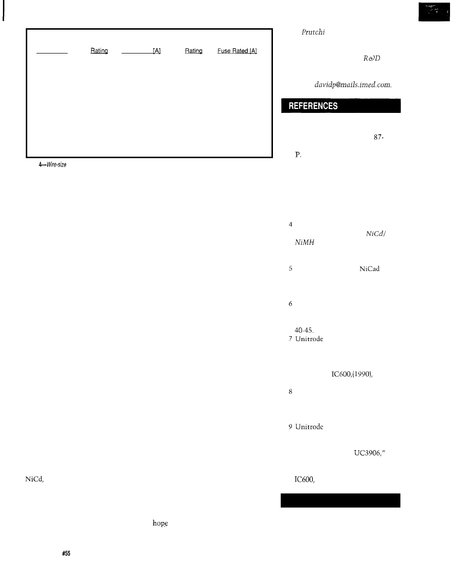
1 5 0 ° C
1 7 5 ° C
Max. Current
Min. for
Max. Current
Min for
Wire Gauae
Fuse Rated
2 6
12
4
14
4
2 4
13
5
15
5.5
2 2
18
7
2 0
7.5
2 0
2 4
9
2 7
10
18
3 5
14
3 9
15
16
3 8
17
4 2
19
14
5 6
2 3
6 2
2 5
12
6 2
3 3
6 8
3 6
10
8 0
4 2
9 0
4 8
8
120
6 0
130
6 9
6
170
8 7
180
9 5
4
2 2 0
120
2 5 0
145
2
2 7 0
160
3 0 0
180
0
370
2 4 0
4 0 5
280
Table
selection is very important in fuse-protected, battery-operated equipment. Minimums are the
absolute lowest recommended values and may cause considerable heating of wires.
Electronic
circuits of small,
primary-battery-powered instruments
can usually be protected by keeping
the batteries in a plastic battery
compartment. For this reason and the
convenience, custom-made enclosures
for consumer products often incorpo-
rate an isolated battery compartment.
The same approach can be used by
the experimenter. A layer of RTV
silicone sealant can be applied to the
walls of the battery compartment to
better protect electronic circuits from
eventual battery leakage. Also, it is a
good idea to use a good-quality battery
holder or battery clip because the
white deposits that alkaline and
mercury batteries develop on their
terminals damage the connectors,
making them unreliable.
Regardless of the rather liberal
design considerations for most primary
batteries, the casing of lithium
batteries deserves great consideration
because of the explosive hazard they
pose. The enclosure of secondary
batteries should be of greater concern
to the experimenter because the risks
involved are chemical and physical.
The current these batteries deliver can
cause wires to heat to the point that a
fire hazard exists.
Although modern sealed-lead-acid,
and silver-zinc batteries
incorporate leak-proof seals and cases,
they seldom can handle the enormous
pressure and heat that develops under
flawed charging (e.g., a high-rate
overcharge) or discharging (e.g., a
continuous short with full charge).
48
Issue
February 1995
Circuit Cellar INK
Good design calls for the use of an
isolated battery box in which all of the
cells of the battery are firmly secured.
All interior surfaces of the battery box
must be coated with a nonconductive,
electrolyte-resistant material. All
unused space must be filled with
absorbent material in case the electro-
lyte leaks. The box must be strong
enough to be able to contain an
explosion. In addition, if the box is
constructed of a conductive material,
the main battery fuses should be
placed inside the box.
Rechargeable batteries often
produce corrosive and/or combustible
gases which must be vented to avoid
concentrating them to the point where
an explosive mixture is generated.
Instruments built for outdoor applica-
tions frequently use a water-tight
enclosure. In these, adequate venting
of gases to the atmosphere must be
ensured. This is especially compelling
when lead-acid batteries are used
because hydrogen and oxygen mixtures
produced during charging are highly
explosive if inadequately diluted.
EVERY DAY LIFE
The use of batteries in portable
electronic equipment is ever more
important in this day of cellular
phones, laptops, and embedded
controllers. Knowing what kinds of
batteries are available and how to
design with them can spell the success
or failure of a product on the market. I
I’ve provided you with a good
starting point for your next design.
q
David
has a Ph.D. in Biomedi-
cal Engineering from Tel-Aviv Univer-
sity. He is an engineering specialist at
Intermedics, and his main
interest is biomedical signal process-
ing in implantable devices. He may be
reached at
1. C. D. S. Tuck, CDS:
Modern
Battery Technology (New
York:
Ellis Horwood Ltd.,
1991)
185.
2.
Horowitz and W. Hill.
The
Art
of
Electronics,
2nd ed.
(Cambridge: Cambridge Univer-
sity P, 1989) 924-926.
3. Gates Energy Products, Inc.,
Rechargeable Batteries Applica-
tions Handbook
(Boston:
Butterworth-Heinemann, 1991).
Maxim Integrated Products,
MAX712 and MAX713
Fast-Charge Controllers,
Data Sheet 19-0100 (October
1992).
D.W. Potter, “Those
Batteries and How to Charge
Them!”
QST
October 1981: 34-
35.
K. Stuart, “Getting the Most
Out of Nickel-Cadmium
Batteries,”
QST
February 1992:
Corporation,
“UC2906 and UC3906 Data
Sheet,”
Linear Integrated
Circuits Data and Applications
Handbook,
4.219-4.229.
W. Dion, “A New Chip for
Charging Gelled-Electrolyte
Batteries,”
QST
June 1987: 27-
29.
Corporation, “Appli-
cations Note: Improved Charg-
ing Methods for Lead-Acid
Batteries Using the
Linear Integrated Circuits Data
and Applications Handbook,
(1990) 9.87-9.97.
413 Very Useful
414 Moderately Useful
415 Not Useful
Firmware Furnace
From the Bench
Silicon Update
Embedded
Ed Nisley
Journey to the Protected
Land: Infrastructure
Improvement
recommended a
‘74 Valiant’s engine
troubles: “Jack up the radiator cap and
drive a new car underneath.” Nearly a
decade later, I sold that Turkey Valiant
for $400; both parties to the transac-
tion thought they got a great deal.
In our last installment, we left a
pair of trivial taskettes swapping
control back and forth in a corner of
the vast expanse of RAM above
1
MB.
This month, we’ll jack up the
taskettes, drive a whole new support
structure underneath, and lower them
gently on a firm foundation.
Each taskette will get a separate
Local Descriptor Table (LDT) with
unique segments, including data
segments allocated on the fly. The task
dispatcher will sprout several new
features, including the ability to
handle an arbitrarily large number of
tasks and a video status display.
If we call our job information
infrastructure improvement, we
can
also be 100% buzzword compliant.
BUILDING AN ISOLATION WARD
It
should come as no surprise that
the ‘386 CPU isolates protected-mode
tasks using segmentation. Restricting
each task to a unique set of segments
ensures it cannot “reach” storage used
by another task. The same CPU
Issue
February 1995
Circuit Cellar INK
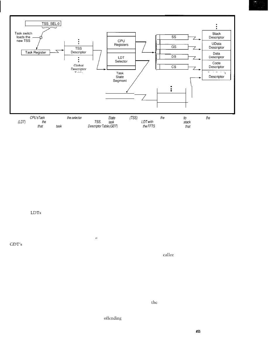
JMP FAR
Table
LDT Register
.
Task Switch
Segment Registers
Local
LDT
D e s c r i p t o r
.
:
Descriptor
Table
Figure l--The
register contains
for the current Task
Segment’s
descriptor. When CPU switches a task, if loads Local Descriptor
Table
register and CPU segment registers from the new
Each
can have a separate
unique code, data, and
segments. The CPU includes
privilege level checks
prevent a
from loading Global
selectors, although
code has not activated
hardware yet.
hardware preventing an errant program
from corrupting its own code works
equally well for tasks. All we need to
do is set things up properly to put that
CISC CPU on our side.
The key to the isolation ward is a
Task State Segment (TSS) field that we
left unused last month-the task’s
LDT selector. The CPU loads this field
into its LDT register during every task
switch. By definition, all tasks have
access to Global Descriptor Table
(GDT) descriptors, but only the
current task may directly access its
LDT. If the
are unique and their
segments don’t overlap, the task is
pretty well bottled up.
The ‘386SX plugs this hole in
grand CISC style by assigning a
privilege level to every segment. Each
descriptor includes a two-bit field
defining the Descriptor Privilege Level
(DPL) and a similar field in each
selector sets the Requestor Privilege
Level (RPL). The DPL field of the
current code segment (the one in the
The alert reader will find no
CS register) sets the task’s Current
reason why a task cannot misuse a
GDT descriptor. For example, the
Privilege Level (CPL).
data alias descriptor grants the
ability to scribble all over the system’s
GDT, a kamikaze gesture that a viral
task might enjoy.
Every time an instruction loads a
segment register, the CPU hardware
verifies that the task is privileged
enough to use the corresponding
descriptor. The most privileged code
runs at Level 0, the least privileged at
Level 3, and there are two intermedi-
ate levels for special purposes.
You may think the levels are
numbered backwards, and I’d have to
agree. The following strangled sen-
tence from the Intel documentation
demonstrates the confusion caused by
inverting the obvious numeric values:
“Instructions may load a segment
register only if the DPL of the segment
is the same or a less privileged level
(greater privilege number) than the less
privileged of the CPL and the selector’s
RPL.
Got that?
Basically, here’s how it works.
“Most privileged” kernel code has
unlimited access to all system facili-
ties, including all GDT descriptors.
Lowly tasks have a “least privileged”
level matching their LDT descriptors.
When a task attempts to access a
“more privileged” GDT descriptor,
hardware triggers a protection excep-
tion, and the operating system termi-
nates the
task.
OK, quickly now, if CPL = 3, DPL
= 2, and RPL = 0, may the task use the
segment?
GDT descriptors may have any
privilege level. For example, your code
might require a shared data segment
available to any task. A “least privi-
leged” GDT descriptor covering that
chunk of storage grants unrestricted
access with no interference from the
hardware privilege checks.
I will punt the entire subject of
privilege levels until we begin working
with tasks in Virtual 86 mode. Split-
ting the Firmware Furnace Task
Switcher (FFTS) code into various
privileges introduces several side
effects that are devilishly hard to
explain without more background, and
this is hard enough already.
FFTS will, however, be structured
along the general lines required by the
privilege hardware. For example, the
tasks use call gates to access system
code even though both the caller and
are both “most privileged” code.
It isn’t exactly safe computing, but at
least we know where our code has
been....
Some manuals describe the
protection-privilege levels as rings.
Typically, there’s a figure showing a
bull’s-eye target with kernel code at
the center and user code on the
periphery. Gaining access to “Ring 0”
in, say, Windows is a coveted achieve-
ment because you can do all manner of
interesting and dangerous things.
Circuit Cellar INK
Issue
February 1995
51
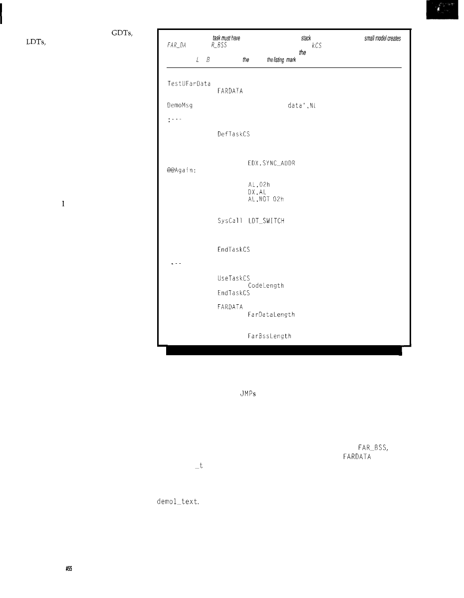
When you understand how
and privilege levels work you
will understand why access to Ring 0
is hard to come by.
But, before all that, we must
create an assortment of unique
segments for our tasks.
SEGMENT SELECTION
Every nontrivial task requires at
least a code segment, stack segment,
and data segment. If the task uses
initialized variables, as most tasks do,
the FFTS task set-up code must create
the data segment and copy the initial
values from the binary diskette image
to the proper addresses. The task may
use other segments requiring addi-
tional set up, as well.
Figure shows how the various
selectors, descriptors, and tables fit
together for a single task. The CPU’s
Task register and LDT register hold
the current task’s TSS and LDT
selectors. The segment-register fields
in the TSS contain selectors referring
to LDT descriptors. Those descriptors
cover the storage segments dedicated
to the task.
In INK 52, I described how the
assembler, linker, and Locate work
together to create the kernel segments
using the small memory model. The
protected-mode start-up code generates
GDT segments that match the usual
real-mode assumptions and allow us to
use ordinary simplified segment
directives. Refer back to that column
to refresh your memory of segment
names, combination attributes,
classes, groups, and suchlike if the
following discussion is too terse for
comfort.
Our tasks, sad to say, cannot use
the small model because each task
must have its own code segment. The
kernel’s single code segment holds all
of the instructions from all of the
source files with offsets relative to the
start of the combined segment. The
code offsets within each task must be
relative to the start of their unique
segment, not the kernel segment, thus
they cannot be combined with the
kernel’s segment.
Apart from that restriction,
though, the small model is ideal for
tasks. The larger memory models
Listing l--Each
unique code, data, and
segments. The
standard
TA
and FA
segments for each source file. The De f Ta s
macro mimics the separate
code segment used in larger memory models without affecting
default near branches in the small
model.
The three A EL directives at bottom of
the length of each segment.
UFARDATA
DD
?
DB
'Demo1 FAR
DB
EOS
endless task loop
PROC
TaskProc
MOV
IN
AL,DX
OR
OUT
AND
OUT
DX,AL
JMP
@@Again
ENDP
TaskProc
mark the end of each segment
LABEL
LABEL
BYTE
UFARDATA
LABEL
BYTE
automatically create a separate code
segment for each source file, which is
good. Within those files, however, the
assembler defaults to
FAR
and
CAL Ls,
which use the real-mode
segment addresses rather than our PM
selectors.
So, I used the small model with a
few macros to create a unique code
segment for each task file. The
segment names are the file name
suffixed with
e x t
in the same
manner as the larger memory models.
For example, the code in
demo 1. a sm
resides in the segment named
The intricacies of MASM and
TASM macro programming are well
beyond the scope of this column. Refer
to Jim Mischel’s Macro Magic with
Turbo Assembler for guidance in this
arcane field. Simple macros are tricky
enough, complex macros keep you
awake at night, and just thinking
about Jim’s macros gives me the
shakes.
Small model programs normally
access the default near data segment
using the DS register. They also have
access to a pair of far data segments
named
FAR-DATA
and
selected with the
and
U FA RDATA
directives, respectively. The
former holds up to 64 KB of initialized
variables and the latter holds up to 64
KB of uninitialized variables. These
two segments sport the
P R I VAT E
combination attribute, preventing the
linker from combining them with
segments from other source files.
That’s exactly what we want for the
task’s data segments!
52
Issue February1995
Circuit Cellar
INK
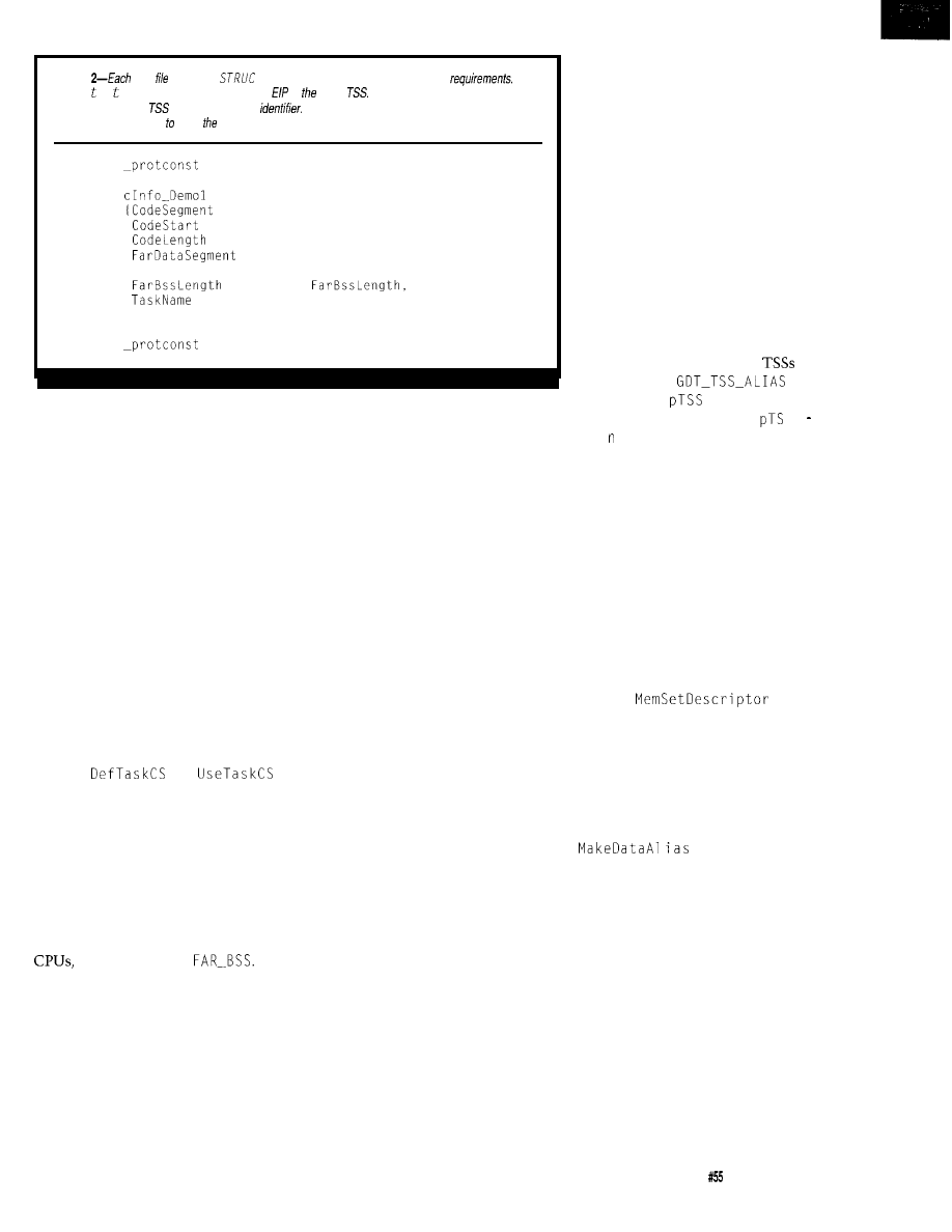
Listing
task contains a
similar to this one summarizing its storage
The
Code.5 a r value supplies the initial value of
in task’s
The initialization code a/so copies
Task Name info the
as an easy-to-read
The real-mode segment and offset addresses
provide enough information create PM addresses
used in the PM segment descriptors.
SEGMENT
LABEL
TASKINIT
TASKINIT
= SEG
TaskProc,
= OFFSET TaskProc,
= OFFSET Codelength,
= SEG
FarDataLength,
FarDataLength
= OFFSET FarDataLength,
= OFFSET
= "Demo Task 1"
ENDS
There is one potential complica-
tion-data accesses must use different
segments depending on whether the
variable is initialized or uninitialized.
Keeping track by hand of which
variable is where can be a major
headache. The assembler is bright
enough to handle the bookkeeping if
we tell it which register points at each
segment.
The normal small model setup
uses DS for the near data in DATASEG,
and the two far data segment selectors
must be loaded as they’re needed. In
our application, the tasks will not have
access to the near data in the kernel’s
segments. Given the limited number
of segment registers, there is no reason
to waste one on inaccessible data.
The
and
macros in Listing 1 include
ASSUME
directives that associate a segment
with each of the segment registers.
The CS register, of course, selects the
source file’s unique code segment. DS,
normally pointing at the near data in
DATASEG, is redirected to FAR-DATA.
GS, one of the additional segment
registers available on ‘386 and higher
selects the task’s
The
assembler automatically uses the
register corresponding to the variable’s
segment and generates a segment
override opcode if necessary.
Although it’s not strictly proper,
each task also has access to the
kernel’s constant-data segment
through the FS register. A truly secure
system will not allow even read-only
access to kernel information. In our
case, the tasks are basically friendly
and won’t attempt to peek at data they
don’t own. They can’t overwrite it in
any case.
Should you feel the need for a
separate constant segment in each
task, use macros similar to those in
Listing 1 with a smidge of task set-up
code to create a read-only data seg-
ment. As with the kernel segment’s
constants, you need not copy them to
a different location because they’re
never changed.
Apart from the macros around the
code segment, Listing 1 resembles any
ordinary real-mode program. Study the
linker map and Locate’s output when
you reassemble these file to see how
they arrange all the segments.
SLICING STORAGE
Before a task is ready for its first
switch, the FFTS kernel must create
GDT and LDT descriptors for each of
its segments, set up the TSS, and
prepare the initialized variables. The
TASKINIT STRUC, showninListing2,
provides all the information FFTS
needs to get the addresses and sizes
right.
Because each task is contained
entirely within a single source file, the
labels at the bottom of Listing
1
mark
the end of their respective segments
and, thus, the segment lengths. The
linker inserts padding between the
data at the end of one segment and the
start of the next segment to ensure
each segment begins on a paragraph
(16-byte) address boundary. The length
of the protected-mode segment
excludes that padding to prevent use of
any “unauthorized” storage.
The best way to see what FFTS
does while creating a task is to study
the big loop shown in Listing 3. Prior
to this loop, the kernel has just
initialized its own TSS to receive the
state of the CPU during the first task
switch. The loop starts out by creating
pTaskInit,apointertocTaskTable,
which is an array of pointers to the
TASK I N I T
structures that are shown in
Listing 2.
As you saw last month,
form
anarrayinthe
segment. The
variable points to
the current TSS in that array;
S
L
i e
a r holds the equivalent linear
address required in descriptor base
address fields.
Each TSS in the array requires two
GDT descriptors: one for the TSS and a
second for the LDT. For simplicity,
each task’s descriptors are consecutive
in the CDT, making the LDT selector
numerically equal to the TSS selector
plus 8. For example, I defined the first
task’s TSS selector as 1000 (hex) and
its LDT selector as 1008. This makes
the task selectors easy to remember:
1000, 1010, 1020, and so on.
The
function
initializes a descriptor in the system
GDT or a task’s LDT. It uses the
descriptor’s selector number as an
index into a data-alias segment
covering the descriptor table to write
the fields. Each LDT requires a
separate data alias, so I wrote
Mem
tocopyadescriptor’s
contents into an unused GDT entry,
set its flags to allow read-write data
access, and return the alias’s new
selector.
The descriptor in LDT[O] is a new
item: a
cull gate.
The CPU protection
hardware prevents a “least privileged”
task from calling a “most privileged”
kernel routine directly. Call gates are
the approved way to pass control
between privilege levels while preserv-
ing protection. They will become vital
when our tasks run at Level 3 instead
of Level 0. We might as well prepare
for that day.
Circuit Cellar INK Issue February 1995
5 3
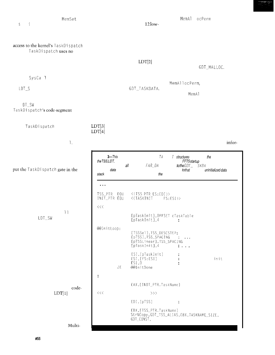
As you can see from
De c r p t o r's
parameters, a call gate
contains the segment selector and
offset address of the privileged kernel
routine. In this case, the gate grants
routine.
parameters, a simplification that I’m
grateful for because I’m running out of
space in this column. We’ll cover the
general case in a month or so.
The
1 macro in Listing 1
creates a
FAR CALL
instruction with
the
W I TC H
selector in the
segment part of the address. When the
CPU executes this instruction, it reads
the
L
I TC H
selector, extracts
selector and offset from the descriptor,
and begins execution at that address.
When
executes a
RET
instruction, the CPU unstacks the
return address and resumes execution
immediately after the Sy s C
a 1
Call gates may live in the GDT
where they are accessible to all tasks
that meet their privilege requirements
or in an LDT for use by a single task. I
LDT primarily to demonstrate that
you can do it this way. One applica-
tion for an LDT gate is providing
different task dispatchers for various
types of tasks. Each LDT would
contain a gate to the appropriate
dispatcher even though the tasks
would use the same Sy s C a branch
with the same
I TCH
selector.
A call gate restricts access to a
single privileged entry point in the
kernel’s code segment. The task
cannot access either the GDT or LDT
descriptors as data (at least when the
proper privilege levels are in effect!)
and, thus, cannot alter the gate
descriptor’s contents. The only two
pieces of information the task needs to
use a kernel routine are its call-gate
selector and the proper parameters.
The remaining LDT descriptors
are more familiar. Creating the
segment descriptor in
requires
converting the task’s real-mode
segment address into the correspond-
ing protected-mode linear address. The
linker and Locate adjust the segment
addresses based on the final location of
the code in the binary image.
plying the segment by 16 (by shifting
left four bits) and appending
order zeros gives the segment’s
starting byte address. The FFTS
diskette loader puts the binary image
at 1 MB, which means the final linear
address is 1 MB plus the real-mode
byte address.
The data segment in
requires a similar computation. In this
case, however, the FFTS start-up code
has already copied the block of far data
from the binary image to a separate
segment covered by
The linear address of the task’s data is
the PM block’s starting address plus
the difference between the real-mode
addresses of the task’s segment and the
far data class.
The uninitialized data segment in
and the stack segment in
are easier. All the task needs is
a segment-register value pointing to an
appropriately sized chunk of storage. I
wrote
1
to
carve the vast
expanse of storage above the FFTS
kernel into useful chunks.
The FFTS kernel extends from the
l-MB line up through the end of the
64-KB block reserved for the task
initialized-data segments. All of the
remaining storage between 00150000
and the end of RAM falls into a single
segment called
There
will eventually be two memory
allocators at work in that block:
whichassigns
“permanent” segments from the top
down, and
1 o
C
,
which parcels
out temporary segments from the
bottom up.
A header preceding each new
block of memory describes the
contents. I include the creator’s task
ID, a short string comment, and a
serial number along with the usual
block address, length, and so forth.
There’s no way to display this
Listing
code steps through an
array of SKI N T
and extracts values
needed for
segments, and
register contents of each task. The
code has a/ready copied fhe
initialized variables in of the tasks’
TA segments TA
TA segment. This code
creates a
segment covering on/y a single task’s contribution
block. The
and
segments are allocated from RAM above
kernel’s fixed locations.
shorthand for the standard pointers
PTR
considerable code omitted >>>
MOV
SUE
correct for pre-inc
ADD
step to next selector
ADD
and TSS entry
ADD
ADD
and table entry
MOV
get pointer to table entry
MOV
get pointer to
info
CMP
if zero, we're done
show task name and copy the string into the TSS
LEA
display code omitted
MOV
set up ES:EDI as TSS ptr
LEA
CALL
\
EAX
(continued)
5 4
Issue
February 1995
Circuit Cellar INK
Listing 3-continued
create the TSS descriptor and pop it into the dispatching array
CALL
\
SIZE TSS,
0
MOV
MOV
MOV
+
MOV
+
(MASK
+ MASK
INC
create LDT selector, descriptor, and LDT data alias
MOV
ADD
MOV
MOV
ADD
PTR
CALL
\
MOVZX
CALL
MOV
set up task switch gate in
CALL
\
set up
and create code segment in
MOV
MOV
MOV
CALL
our CS
MOVZX
convert task seg
SHL
to linear
ADD
EAX,EBX
code seg + task seg
CALL
\
set DS and create the task's data segment in
the startup code copies the initialized values into
all we do is set the starting point and length of our data
MOV
MOV
SUB
MOVZX
SHL
CALL
ADD
far data seg base
BX,SEG
far data class base
EBX,BX
convert to linear
EAX,EBX
MOV
CALL
set GS and allocate the task's uninitialized data seg in
if allocation fails the task fails with a data segmen t error
MOV
SOLID STATE DISK $135”
Card
2
Emulator
EPROM,FLASH
Program/Erase FLASH On-Board
Total, Either Drive Bootable
25MHZ 386DX CPU
Compact AT/Bus or Stand Alone
IDE, FDC, 2
Drives to
Cache to
DRAM to 48M
TURBO XT
w/FLASH DISK
To 2 FLASH
Total
DRAM to 2 M
FLASH On-Board
CMOS Surface Mount, 4.2” 6.7”
2
Par, Watchdog Timer
Tempustech VMAX products are
PC Bus Compatible. Made in the
J.S.A., 30 Day Money Back Guarantee
*QTY 1,
breaks start at 5 pieces.
TEMPUSTECH, INC.
634-0701
Fax for
fast response!
295
Airport Road
Naples, FL 33942
Circuit Cellar INK
Issue
February 1995
yet, but we’ll be glad it’s there
when we need it!
You have surely seen this method
of memory allocation in real mode.
The nice thing about protected-mode
allocators is that they can create a
segment descriptor that exactly covers
the block of storage. The descriptor
does
not
include the header, so there is
no way to corrupt the kernel’s infor-
mation. As always, the CPU triggers a
protection exception when the task
attempts to write beyond the bounds
of the segment.
I’ll have more to say about
memory allocation later on when the
tasks need dynamic memory. An
obvious application will be replacing
the static message buffer in St r
Format with a temporary buffer that’s
allocated on each call.
After the LDT is complete, the
start-up code sets the task’s FS register
to the rot c o n s t segment, puts the
TSS selector in its EAX register, and
displays the finished TSS and LDT.
The task is finally ready for its first
activation!
Complex, yes, but from the task’s
point of view the setup is entirely
invisible. Each task gets control on the
first task switch with its segment
registers preloaded, a clean stack, and
all the variables it needs. Tasks invoke
the dispatcher with a FAR CALL (using
the C a 1 1 macro) and regain control
as though the whole kernel is just a
function.
Now, for that first task switch..
CENTRAL DISPATCHING
Once you allow more than one
task in your system, a decision rears
its ugly head: which task to run next!
There are at least as many solutions as
operating systems, each optimized in a
different direction.
Although the buzz phrase nowa-
days is “preemptive multitasking,”
we’re going to start out with a much
simpler method-cooperative multi-
tasking with round-robin dispatching.
Although it’s not at the cutting edge, it
will serve our purposes for quite a
while.
“Cooperative multitasking”
means each task runs until it returns
control to the Ta s k i pa t c h routine.
Listing 3-continued
CALL
\
\
allocate task
if allocation
CALL
stack with
descriptor, set
fails, the task fails with a stack segment error
\
MOV
allow unused DWORO
MOV
; set the remaining task registers
MOV
global constants
MOV
tell task its TSS
MOV
; discard the LDT alias and display the complete TSS
CALL
CALL
show what we did
JMP
do another task
The advantage is that the task itself
determines when it should yield
control to the dispatcher, thus elimi-
nating much of the need for sema-
phores and operating-system inter-
locks. The disadvantage is that a single
task can fall on the ball, never call
and wedge the entire
system.
Lest this sound entirely too fragile
for words, it’s how Windows works.
We’re starting with simpler and
behaved tasks than your average
Windows application, increasing the
odds that things will keep clocking
along as desired.
“Round-robin dispatching” means
the task dispatcher iterates through all
the tasks in a fixed order. This algo-
rithm gives every task the same
priority and, not coincidentally,
eliminates a lengthy discussion of
priority management. Idle tasks may
return to the dispatcher immediately,
hardworking tasks may gnaw through
a large chunk of computation, and
everybody gets a share of the CPU at
least once in a while.
Listing 4 shows the new Ta s k
i s pa t c h routine. The task set-up
code loads D
i
r ray with the TSS
selectors and control flags as it creates
each task. The kernel task occupies
D i s r ray 0 and passes control to
onthefirst
task switch. The dispatcher continues
through each entry until it finds a zero
Tas
flag, at which point it
resets D i p I n d e x and starts over again
with the kernel task.
provides a way to skip a task that
doesn’t need dispatching. Some
functions, such as error and interrupt
handlers, require separate tasks that
should not be dispatched by the
operating system. This flag comes in
handy next month when we explore
those topics. For now, it’s just a
placeholder. All our taskettes are
eminently dispatchable!
If your system has a video display,
you can watch the task dispatcher in
action. Each pass through Ta s k
i pat
c
h updates a status line on the
bottom of the CRT with the current
56
Issue
February 1995
Circuit Cellar INK
D
i p I n d e x,
TSS selector, and cumula-
tive number of task switches. Bit 15 of
the FDB DIP switches turns this
display off. Watch the FDB LED digits
to see how that affects
ing performance.
The
trace outputs reveal
that one iteration of each trivial
this month requires about 40
us on a
‘386SX. Computing
and writing the status values to the
screen adds about 700 to each task
switch. A single pass through the four
Di
entries thus requires 160
us with tracing disabled and 3 ms
when you watch the numbers blurring
on the screen.
The video status requires an
unseemly proportion of time simply
because the tasks aren’t doing any-
thing. Keep this in mind when you
start writing your own code.. .and keep
that scope handy!
IS IT WORTH IT?
By
this time, your head is un-
doubtedly reeling from all the
(Three-letter Acronyms), segments,
selectors, descriptors, pointers, and
whatnot. Indeed, the single biggest
challenge of this entire series has been
explaining how the myriad segments
fit together. You’ve certainly wondered
why I didn’t opt for flat
PM
programming-set the segments to
span all of the PC’s storage and be
done with this nonsense!
Most of the articles and columns
you’ve read elsewhere deal with PM
programming for a particular operating
system. Whether the author uses
the long-awaited
Windows, a
DOS extender, or one of the *NIX
crowd, the conditions under which the
code runs are fixed. If the OS sets up
the segment registers so the user code
runs in flatland, well, then they write
flat
protected-mode code.
In our case, the FFTS
is
the
operating system, rudimentary though
it may be. If I were writing a single
protected-mode program on bare
silicon, we’d be done now-flip into
32-bit protected mode, set a few GDT
segments, ignore memory protection,
bypass multitasking, and go!
But, that treats the ‘386 as a
glorified
and limited. If
your problem is complex enough to
justify a ‘386 embedded controller
running in protected mode, it’s
probably also complex enough for
multitasking. If it’s
complex,
those tasks should be protected from
each other. The ‘386 has that protec-
tion built right into the hardware.
So, here we are with all those
segments. It’s a dirty job, but
somebody’s gotta do it.
And that’s why I’m going through
this exercise. You can tear off what-
ever chunk of FFTS fits your require-
ments. The code in INK 52 can serve
as the basis for a flat
program if
you twiddle the GDT descriptors just a
bit. The code last month is the
simplest possible hardware-assisted
multitasker. The
this month lay
the groundwork for a more robust
multitasker that makes the tasks
easier to debug.
Just wait until we get closer to
Virtual 86 mode because the CPU
requires paging to run more than one
I
__
6" x 7". HAL
is sensitive enough
to even distinguish different conscious states-between concentrated
mental activity and pleasant daydreaming.
HAL
gathers all relevent alpha,
beta, and theta brainwave signals within the range of
4-20
Hz and presents
it in a serial digitized format that can be easily recorded or analyzed.
HAL’s
operation is straightforward. It samples four channels of analog brainwave
data
64
times second and transmits this digitized data serially to a PC
at
4800
bps. There, using a Fast Fourier Transform to determine
amplitude, and phase components, the results are graphically displayed
HAL-4
KIT...... N
E W
P
A C K A G E
P
R I C E
$279
Contains HAL-4 PCB and all circuit components, source code on PC diskette,
serial connection cable, and four extra sets of disposable electrodes.
to order the HAL-4 Kit or to receive a catalog,
CALL:
(203) 8752751
OR FAX:
(203) 8752204
C
I R C U I T
C
E L L A R
K
I T S
l
4 P
A R K
S
T R E E T
S
U I T E
1 2
l
V
E R N O N
l
C T 0 6 0 6 6
-The Circuit Cellar
Level detector is presented as an
example of
the
techniques used
brainwave signals.
Hemispheric Activation Level detector is
not a
approved
no medical claims are made for
device, and it should not be used for
medical
purposes. Furthermore, safe use requires HAL be battery operated
Circuit Cellar INK
February1995
Listing
task initialization code Listing 3 creates
an array of
selectors and control
with
the kernel task as the first entry. The kernel task
this
to switch to the next task in the array and
the process continues each time control returns here. Each pass reads the
switches to
control the
video status output through the r c I f and
c En d I f macros.
CODESEG
PROC
FAR
USES
set up DS to kernel's data to reach the dispatching variables
MOV
MOV
CALL
sample the switches for tracing
select and dispatch the next task
a simple round-robin run through all the tasks in the array
; we dispatch the kernel task (index = every time
MOV
get current task index
INC
EBX
step to next task in array
MOVZX
+
TEST
EAX,MASK
entry in table?
JNZ
1 = yes, so do it
XOR
EBX,EBX
; 0 = no, hit the end
JMP
always run kernel!
TEST
OK to run this task?
JZ
no, skip it
MOV
save new task index
update the trace display
MOVZX
+ EBX*SIZE
CALL
CALL
do the task switch
MOV
mark the start in the old task
IN
OR
OUT
DX,AL
MOV
aim at new task pointer in table
JMP
PTR
+
IN
AL.DX
mark the end in the new task
AND
AL,NOT
OUT
INC
count this task switch
return to the new task
the FAR PROC forces this to be a FAR RET...
RET
ENDP
V86
task. Although I don’t plan to use
virtual memory, paging allows us to
run each task in, yes, absolutely flat
3%bit protected mode. It doesn’t get
simpler than that, even though the
behind-the-scenes code is something
fierce.
And, that sounds like something
worth knowing!
RELEASE NOTES
The code this month builds three
trivial taskettes in addition to the
kernel. Each step in the process sends
a torrent of trace messages to
make sure you turn on your
program’s screen capture! Once
everything is ready, the four taskettes
run in round-robin order while the
dispatcher updates a status line on the
bottom of the video display.
If your system has a Firmware
Development Board, you can selec-
tively throttle the torrent of informa-
tion by flipping DIP switches 15
through 11. Bit 15 controls the video
status display. Watch the FDB
to
see the effect of turning the status off!
The remaining switches control
various tracing options in the task and
memory routines.
Next month, we’ll make the call
gates more formal, add a conforming
code segment, and run into a brick
wall or two. Stay
q
Ed Nisley, as Nisley Micro Engineer-
ing, makes small computers do
amazing things. He’s also a member of
Circuit Cellar INK’s engineering staff.
You may reach him at
or
Software for this article is avail-
able from the Circuit Cellar BBS
and on Software On Disk for this
issue. Please see the end of
in this issue for
downloading and ordering
information.
416
Very Useful
417 Moderately Useful
418 Not Useful
Circuit
Cellar INK
Issue February 1995
5 9
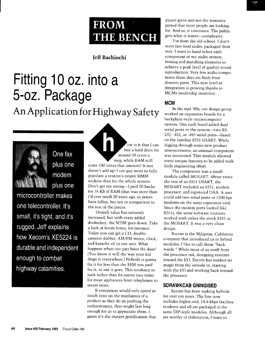
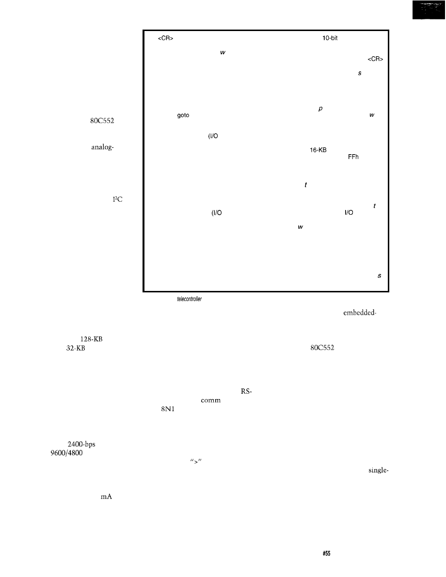
introduce you to a new level of
integration-the XE5224 series
module. This telecontroller incorpo-
rates a micro along with the UART,
modem, and DAA into a packaged
module measuring 2.75”
x
1.38”
x
0.5”
(see
Photo 1).
Although future plans include a
number of different processors, the
first to be released is an 8031 core.
Actually, it’s a Signetics
processor. The Signetics microcontrol-
ler has an S-input, IO-bit A/D con-
verter built-in, so it adds
sensing capabilities to the XE5224.
The 26 additional I/O bits fill out the
digital portion with many of the lines
providing alternate functions. These
functions include real-time clock/
calendar, two PWM outputs, an
bus, a console serial port, watchdog
enabie, and external interrupt and
counter/timer inputs.
As most of you know, the 8031
can access 64 KB of data space and 64
KB of program space. The XE5224
includes a 32-KB SRAM for the lower
portion of the data space and a 32-KB
ROM (with programmed monitor and
telecontroller software) for the lower
portion of program space.
The upper 32-KB space is over-
lapped into a combined data and
program space. It is composed of 32
KB of flash memory. The flash
memory is actually a
device,
broken into four
pages. These
pages can be switched in and out of the
lower 32 KB of program space and/or
the upper 32 KB of data and program
space. The configuration of the RAM,
ROM, and flash memory is set through
external pins. The variety of memory
combinations this setup produces
makes this module flexible in form
and function.
In addition to the processor,
Xecom embeds a
modem and
an optional
send/receive
fax. The included DAA enables legal
connection to the phone line for
instant product acceptance.
Current consumption at 5 V for
the XE5224 is less than 100
with
the modem active and about half that
with the modem in sleep mode.
Although the hardware clock/calendar
requires an external source (battery or
A x
analog
input (O-7)
monitor displays
conversion of
analog channel x
c w
change address
monitor displays address wand allows
user to change, <space> to skip,
alone to end
D s e
display data-memory contents
monitor displays from address to
address e
E s e
display program-memory contents
monitor displays from address s to
address e
F s e p
fill data memory with pattern
monitor fills from address s to address
e with pattern
G w
address w
monitor jumps to program address
and executes
H
on-line help
monitor displays these commands
I X
digital input
address)
monitor displays byte read from
address x
K x
kill flash section (O-3)
monitor fills
section x of active
flash memory pages with
L s e t
load data space from program space
monitor moves a block of program code
starting with address sand ending with
address e to data space starting at
address
M s e t
move data block
monitor moves a block of data starting
with address sand ending with address
e to data space starting at address
O x d
digital output
address)
monitor outputs byte d to
address x
R W
read in a hex file
monitor accepts Intel hex file and applies
offset prior to storage in the program
space
T
“AT” command mode
monitor enters the modem command
mode. No command prompt, #to exit
back to monitor
V
version information
monitor displays version banner
W s e
write out a hex file
monitor writes an Intel hex file of the
program space starting with address
and ending with address e
Table
l--The
comes with built-in debug and monitor commands to aid in program development
supercap), the use of nonvolatile flash
memory eliminates this need for data
and/or program storage.
it, external modems are
processor based.
PRELOADED TELECOM
FIRMWARE
Xecom provides a terminal
emulator program for the PC which
allows you to talk directly to the
XE5224 through a user-supplied
232 interface. (Any
program
using
parameters works.) The
auto-baud feature looks for a space
character and returns a sign-on
message indicating a link is made and
the debugging monitor is active. Data
rates from 300 to 38,400 bps are
supported. The
character prompts
you to input a command string. Table
1 gives a sample of the monitor
commands.
This is exactly the concept Xecom
uses. Although it looks like an I/O
device to the
processor, the
modem port is actually an embedded
microprocessor which shuffles parallel
information and acts like a Hayes
modem with the standard AT-com-
mand set (see Table 2). This takes
much of the load off the ‘552, freeing it
to do its own thing. The fax com-
mands operate on Class 1 protocol and
can be found in Table 3.
ENVIRONMENTAL RUGGEDNESS
Many personal computers today
use multiple processors. Each proces-
sor is responsible for an individual
function such as video or audio.
Although most of us may not realize
Neglecting the telecontroller’s
most obvious advantage (its size), what
makes it so different from other
board micros? I get the same feeling
handling one of these modules as I do a
DC/DC converter or a high-power,
solid-state switch module-a sense of
ruggedness and power. Potting com-
pound encapsulates every component
into a single mass. The potting
Circuit Cellar INK Issue
February 1995
61
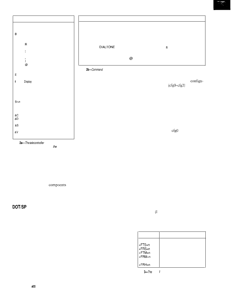
AT Commands
AT
Command-line prefix
A
Answer incoming call immediately
Al
Reexecute last command line
Answer tone
Dn
Dial telephone number n;
P Pulse dialing
Originate call in answer mode
T Touch-tone dial
Return to Command Mode
after dialing
Pause
0.5-s hookflash
Wait for silence
W Wait for dial tone (default
30 s; see register S7)
Command
Echo
H
Off-hook control
product code
L
Volume control
M
Speaker control
0
On-line control
Q
Result codes (default)
Sr?
Read and display value of register r
Set register r value to n
V
Word/numeric result codes
X
Response set
Z
Reset
DCD control
DTR control
&F
Load default
DSR control
&T
Test modes
Displays active user
selected profiles
Table
supports a standard
Hayes A T-command set to minimize programmer
learning curve.
provides physical protection from the
environment and a platform in which
all components remain at a stable
temperature.
When equipment has to withstand
severe environmental extremes, it is
prudent to design with
most likely to survive. I believe our
interstate highway system would
benefit from technology such as this.
The Department of Transportation
in conjunction with the State Police
act as a medical team to keep our
asphalt arteries clean and unrestricted.
If it were not for these dedicated
personnel, civilization as we know it
would certainly collapse. To help these
professionals respond with the speed
and intuition of an oracle, I wish to
suggest an Auto Informer-an alterna-
tive to the present data-collection
systems.
We are beginning to see the use of
inductive pickups because of their
simplicity. They are weather and
Digit
Code
Word Code Meaning
0
OK
Successfully executed command line
1
CONNECT
300 bps connection established
2
RING
Ring signal detected
3
NO CARRIER
Carrier not detected within Register S7 detect time
4
ERROR
Error found in command line: returns to command line
5
CONNECT 1200
1200 bps connection established
6
NO
No dial tone detected within 5 after going off-hook
7
BUSY
Busy signal detected after automatically dialing a call
8
NO ANSWER
Five seconds of silence was not detected when using
the
command in the Dial command line
10
CONNECT 2400
Connection established at 2400 bps
Table
responses also match those used by most A T-type modems, so ease code development.
minimum of signal conditioning
traffic resistant. The sensor’s signal
hardware.
output determines mass and even the
speed of a moving body by examining
the waveshapes it produces. Multiple
lanes can be easily monitored using a
The telecontroller monitors these
lanes, keeping track of the traffic’s
speed, relative spacing, and the
numbers of cars and trucks using a
specific lane. The telecontroller stores
and/or reports this information with
time and date stamps.
Analog inputs monitor air and
road temperatures as well as humidity
and precipitation. Large message signs
can instantly relay driving conditions
to motorists via a serial interface from
the telecontroller.
flash memory using the “K” command
code space at OOOOh with the
and download an Intel hex file into it
using the “R 8000” command. The
ration jumpers
set to 000.
8000 is a hex offset used to place an
object file (created to run at OOOOh)
This places flash memory page 0 at
into the flash memory (page 0) at
8000h. When the
jumper is
changed, the flash memory (page 0) is
8000h.
relocated to OOOOh, replacing the
monitor. The program in memory
With the monitor, I can erase the
executes automatically after reset (or
powerup).
Most important, the telecontroller
can make telephone and fax calls to
report dangerous situations like
stopped traffic or icy conditions. This
action may be a simple fax to the
headquarters notifying them of the
situation or, in a highly integrated
system, the action may modem a
central processor. This computer
would collect and correlate informa-
tion from each telecontroller. It could
determine alternate routes for traffic or
necessary changes to posted speed
limits. Suitable messages would
be relayed back to the appropriate
telecontrollers by modem and
displayed for the motorists.
QUICK AS A FLASH
I wanted to experiment with
the telecontroller’s use of flash
memory for program storage and
execution. The telecontroller’s
ROM-based debugger occupies a
In addition to being relocated, the
flash memory is now write protected,
which makes development a breeze.
There are no EPROMs to burn. Hey!
Wait a minute. Did I just suggest that
writing a program in assembler or C
was a breeze?
If you follow this column on a
regular basis, then you know I can’t
stand spending hours and hours at a
terminal writing code. And, when I
can get away with it, I like to use
BASIC understand a future version of
the telecontroller may be available
with embedded BASIC). In addition,
the user has at his disposal a multitude
Command
+FCLASS=n
+FTH=n
Table
Class
various fax features.
Description
Select fax class
Stop transmission and wait
Receive silence
Transmit data
Receive data
Transmit data with HDLC framing
Receive data with HDLC framing
command set offers control of
the
62
Issue
February 1995
Circuit Cellar INK
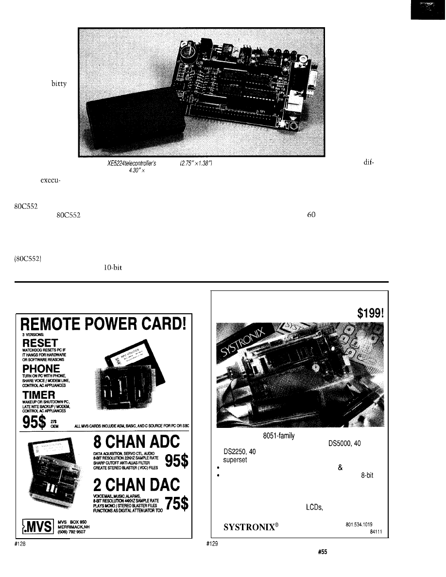
of C library
routines. How-
ever, to put this
hardware through
its paces today, I
am forced to get
down to the
gritty. Well,
almost.
A few years
ago, I did a column
on magnetic
levitation and
used a BASIC
compiler for
speed-speed in
development and
speed in
the highway’s
road bed. (I think
this would be a
great project for
fuzzy logic using
only single lane
sensors, but
that’s not my
intent-at least
not in this
article.)
Using dual
sensors allows for
easy speed and
size detection.
Photo l--The
small size
influenced the
development board’s maximum
allowable dimension of
2.60”.
The time
ference between
tripping the first
tion. It’s time to pull this back off the
shelf and try integrating it with the
to create an executable file.
Since the
is an offshoot of
the 803
1
core, I can compile a BASIC
program and execute it as an 803
1.
However, I need some assembly
routines for accessing any on-chip
functions that I might wish
to take advantage of
(e.g.,
the
A/D converter). The BASIC compiler
allows in-line assembly code to be
integrated right along with the BASIC,
so it isn’t entirely a hodgepodge.
MONITORING OVERVIEW
In our highway application, speed
and volume monitoring is based on
timings calculated from dual, buried
mass sensors installed in each lane of
sensor and the second sensor gives the
speed of the passing mass. If the
sensors are offset by four feet, a vehicle
travelling at mph passes the
sensor’s trip points in 44 ms.
The length of time the mass
spends over the first sensor in com-
parison to its speed determines the
size of the mass. In gross terms, if the
same vehicle remains over the first
CTLVOLT
5 YEAR LIMITED WARRANTY
F R E E S H I P P I N G I N U S A
NEW! UNIVERSAL DALLAS
DEVELOPMENT SYSTEM
from
l
It’s a complete
single board computer!
l
One board accommodates any 40 DIP
SIMM
SIMM DS2252, or 72 SIMM DS2251, 8051
processor! Snap one out, snap another in.
Programs via PC serial port. Program lock encrypt.
LCD interface, keypad decoder, RS232 serial port,
ADC, four relay driver outputs, four buffered inputs.
l
Power with 5VDC regulated or 6-13 VDC unregulated
l
Large prototyping area, processor pins routed to headers
l
Optional enclosures, keypads,
everything you need
l
BC151 Pro BASIC Compiler w/50+ Dallas keywords $399
TEL: 801.534.1017 FAX:
555 South 300 East, Salt Lake City, UT, USA
Circuit Cellar INK
tssue
February 1995
6 3
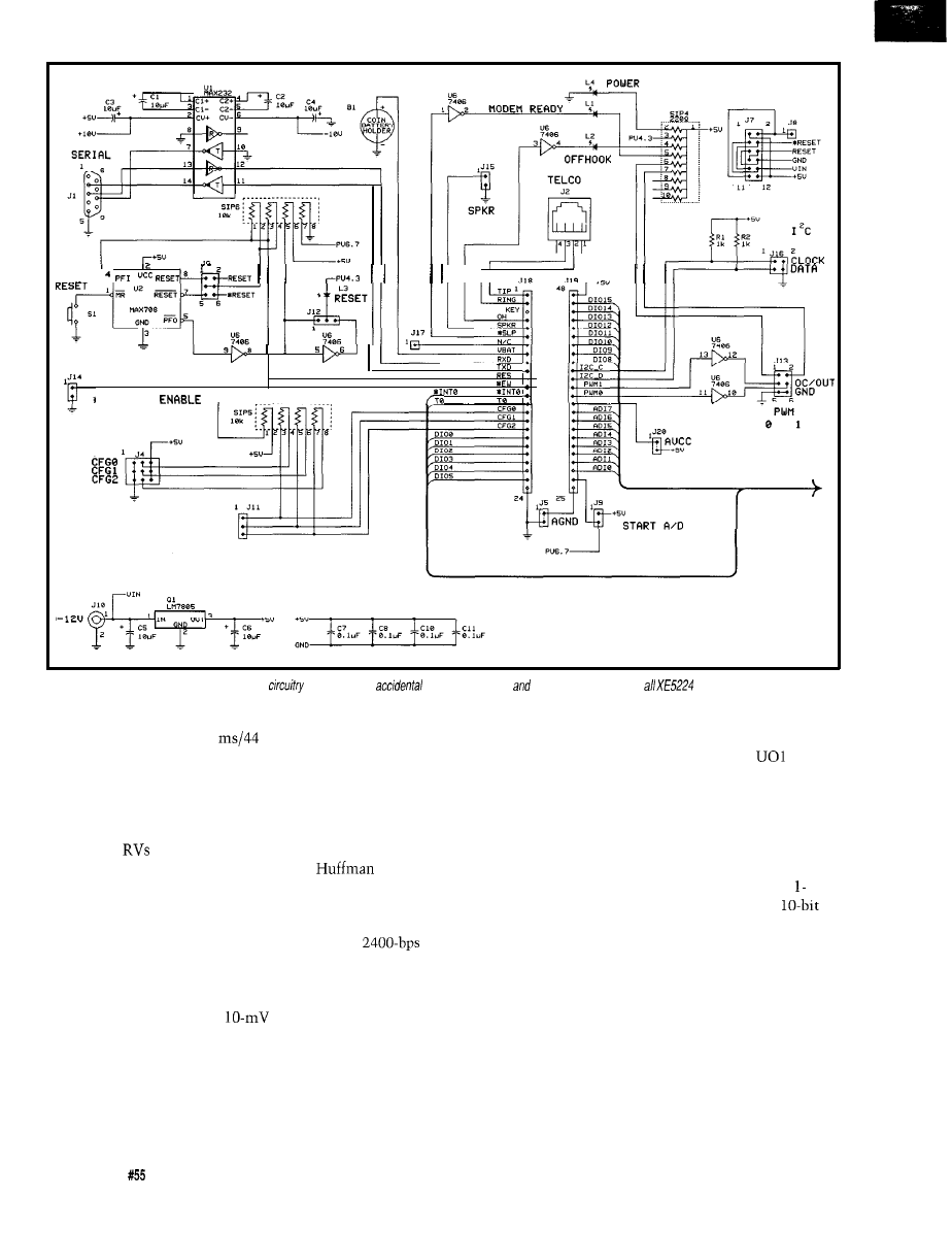
I
I i
*WATCHDOG
CONUERSION
Figure 1 a--The development board adds support
which prevents
module destruction
provides easy access to
functions.
sensor for 132 ms, it is three time
units by four feet (i.e., 132
ms x
4’) or twelve feet. The high, low, and
average speeds are saved for each lane.
The volume is broken down into three
groups: autos and motorcycles are
recorded as small vehicles, single-box
trailers and
as medium vehicles,
and double-box trailers and some
hauled, heavy-construction equipment
as large vehicles.
Monitoring the air and road-bed
temperature is extremely important in
this application. Your choice of sensor
determines what (if any) sensor
calibration may be necessary. Silicon
temperature sensors output
per
degree (negative output for negative
temperatures). By adjusting the offset
and gain of the incoming signal to take
full advantage of the A/D converter’s
O-5-V input, it’s possible to get 0.5”
resolution.
PUTTING IT ALL TOGETHER
command strings since they are a mix
Although I wanted to use the
of text and values. (An output driver
optional fax modem for sending
accessed through BASIC’s
command would make this operation a
breeze.)
recorded data, I did not want to go
through the hassle of breaking down
the data characters into line-scan bits.
The line-scan bits, of course, have to
be converted into the modified
code necessary for facsimile
transmissions. Ugh, another potential
article.
This time, I’ll be satisfied with
simple
data modem trans-
missions. The telecontroller makes a
call to the central computer at hourly
intervals or whenever a dangerous
situation occurs. The central office can
also call the telecontroller to ask for
the latest data.
The modem’s AT command set
(Table 2) allows the micro easy access.
The most difficult part of modem
communications is parsing the output
WRAP UP
All told, I’m really impressed with
this little package. There is an estab-
lished core audience for this 803
family device. The digital and
analog I/O are ample for most applica-
tions. The inclusion of the hardware
clock/calendar and integrated modem
complements the processor’s power
rather nicely.
I liked this module so much I
designed a small 2.5” x 4” interface
board (see Figure 1) to help in the early
stages of software and hardware
development. I know before you
develop a piece of hardware that uses
the telecontroller, you will want to
64
Issue
February 1995
Circuit Cellar INK
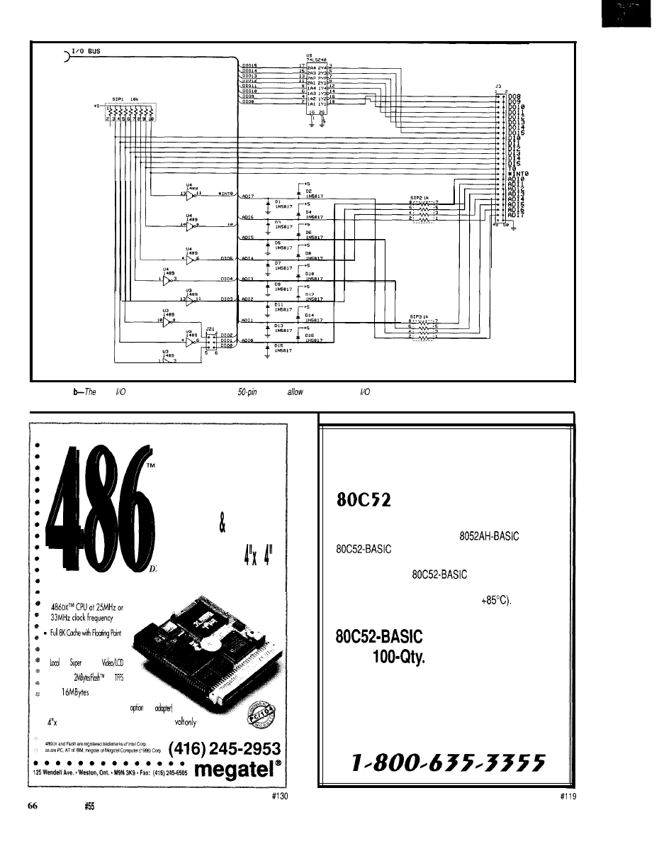
Figure 1
digital is brought out to an industry-standard
header to
the use of external backplanes.
l
WORLD’S SMALLEST
Embedded PC with
Floating Point,
Ethernet Super
X
VGA Only
The
PC/II +i
includes:
l
l
Ethernet local Areo Network
l
Bus
VGA
l
Up to
with
l
4 or
User DRAM
l
PC/l
04 or ISA Bus compatible
[with
.
4” Format; 6 watts power consumption at t5
MOVE OVER INTEL
MICROMINT SOURCES
CMOS BASIC CHIP
Micromint has a more efficient software-compatible suc-
cessor to the power-hungry Intel
chip. The
chip was designed for industrial use and
operates beyond the limits of standard commercial-grade
chips. Micromint’s
chip is guaranteed to
operate flawlessly at DC to 12 MHz over the entire
industrial temperature range (-40°C to
Available in
40-pin DIP or PLCC
chip
$19.00
OEM
Price
$12.00
BASIC-52 Prog. manual $15.00
MICROMINT, INC.
4 PARK ST.
l
VERNON, CT 06066
TO ORDER CALL
Issue February1995
Circuit Cellar
INK
play a bit with it. Well, this will get
you started at full throttle.
The DE9 connector and RS-232
interface enable developers to make an
easy console connection. The
5-V regulator and power jack make
stringent regulated-power-supply
requirements unnecessary.
Xecom hints at using other micro
cores in the future. To prepare for that
possibility, I chose to use a MAX708
hardware reset. This ensures suitable
reset timing and both polarities of
reset for future products. Four
indicate status of reset, power,
modem ready, and off-hook conditions.
To reduce the potential damage to
the telecontroller, I added protection
to both the TTL and analog I/O.
During the development stages, TTL
I/O is protected by buffering the inputs
for high-voltage
The outputs
are buffered or inverted by using either
a ‘240 or a ‘241. Analog inputs are
protected by
resistors and
diodes tied to the
supply rails. All I/O is available on a
header that is compatible with
industry-standard I/O racks.
connections are through a standard
11 connector.
All together, it’s a pretty nifty
combination.
q
Bachiochi
AH-key”) is an electrical engineer on
Circuit Cellar INK’s engineering
staff.
His background includes product
design and manufacturing. He may be
The following are available from:
Xecom, Inc.
374 Turquoise St.
Milipitas, CA
(408) 9456640
Fax: (408) 942-1346
Micromint, Inc.
4 Park St.
Vernon, CT 06066
(203) 871-6170
Fax: (203)
XE5200 (Blackjack 552)
(controller only) $
1
3
9
(Blackjack 552DM)
Telecontroller
(with data
modem) . . . . . $199
(Blackjack 552FD)
Telecontroller
(with fax and
data modem) Call for pricing
Blackjack Protective Demo
Board . . . . . . . . . . . . . . . . . . . . . . . . . . . . . . . . . . $99
The XE5200
family is available
second
by Micromint
under the tradename Blackjack 552.
BC15 1 BASIC Cross-Compiler
(integer math)
Systronix, Inc.
754 East Roosevelt Ave.
P.O. Box 526398
Salt Lake City, UT 84152
(801) 487-7412
419
Very Useful
420 Moderately Useful
421 Not Useful
Bar Code Sensor
Battery Controllers
Clock/Calendars
Digital Power Drivers
DTMF Phone Interfaces
Firmware Furnace Widgets
HCS-II Hard-to-find Parts
Bus
Photodiodes
Data Link Parts
Remote Control
Laser Diode Controllers
Linear Hall Effect Sensor
Multiplexers Crosspoints
Power Op Amp
Remote Temperature Sensor
Stepper Motor Drivers
Watchdogs Power Monitors
8051 Information
and
more!
Use a soldering iron? Get the parts!
UPS.
day $6 5019.00 to 48 US states, COD add $4.50 PO Boxes and
addresses: $6 for USPS mall. Check, MO, or COD only; no
cards,
no open
NC
add 6% sales tax.
at five parts.
Data sheets included with all parts.
Call/write/fax for serious/y tempting catalog...
Unobtainium
Your unusual part5 source
13109 Old Creedmoor Road
Raleigh NC 27613-7421
FAX/voice (919) 676-4525
The BCC52 controller continues to be
Micromint’s best selling single-board com-
puter. Its cost-effective architecture needs
only a power supply and terminal to become
a complete development system or
board solution in an end-use system. The
BCC52 is programmable in BASIC-52, (a
fast, full floating point interpreted BASIC), or
assembly language.
The BCC52 contains five RAM/ROM
sockets, an “intelligent” 27641128 EPROM
programmer, three
parallel ports, an
auto-baud rate detect serial console port, a serial printer port, and much
more.
PROCESSOR
CMOS processor
counter/timers
*Console RS232
detect
Line
RS-232
Three B-bit parallel ports
EXPANDABLE!
BCC
boards
B C C 5 2
Controller board
BASIC-52 and RAM
$189.00
Low-power CMOS
the BCC52
$ 1 9 9 . 0 0
-40°C to
temperature version
$ 2 9 4 . 0 0
Low-power CMOS, expanded
RAM
$ 2 5 9 . 0 0
CALL FOR OEM PRICING
MICROMINT, INC.
Europe
Canada, (514)
Welcome!
Circuit Cellar INK Issue
February 1995
6 7
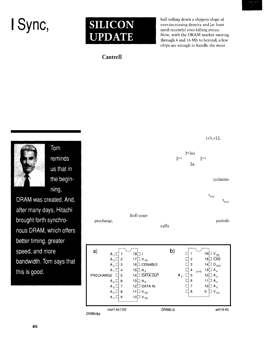
Therefore
I DRAM
READ/WRITE
V ss
D
IN
W E
RAS
A *
A ,
V
D D
Tom
bloated software upgrades without
blinking a bit.
The modern DRAM era began in
the late ’70s with a 16-Kb DRAM such
0
as the Intel 2116 illustrated in Figure
lb. More important than the technical
features, acceptance of a standard
kicked off multisourced DRAM as a
hese days, Intel
commodity. The subsequent brutal
is mainly known as
battles for sockets had great benefits
the company that, in
for users, but drove many suppliers
concert with Microsoft,
(including Intel) from the business.
controls what goes on inside most
PCs. Their commanding position has
served them well, propelling them to
the top of the IC business.
After a decade of PC and x86
hoopla, it’s easy to forget Intel’s earlier
contributions at the dawn of the
silicon revolution. Long before the
x86, Intel invented a chip that is
arguably even more important-the
DRAM.
Looking back at chips like the
early ’70s’ Intel 1103 (see Figure la) is
always good for a laugh. Imagine what
your typical 1 -MB PC would be like if
it had 8000 of these little puppies.
Forget the mini- and maxi-tower
enclosures; the Trump tower is more
like it. You’d better beef up your
power supply too since each 1103
burned a half watt or so.
own
inverted DOUT, and
DRAM101
Though the 2116 came (and went)
before the x86, most of its features
persist to this day. Thankfully, a single
supply replaces the three
and
-5 V) of yesteryear, but otherwise
DRAM
S
haven’t changed that much.
A typical
DRAM is orga-
nized as
rows and
columns. As
shown in Figure the row address is
strobed into the DRAM with RAS*
[row-address strobe). Next, the column
address is strobed with CAS *
address strobe], which also clocks the
data in or out depending on the WE*
pin. The timing parameter
denotes
the access time of the DRAM (i.e.,
is 70 ns for a “70-ns DRAM”).
To refresh your memory (ho-ho),
DRAM
S
store each bit on a capacitor
that leaks. Thus, they must be
16-V I/O levels just add to the fun.
refreshed, usually a row or two
Nevertheless, as feeble as it now
(limited by power considerations) at a
seems, the 1103 started the DRAM
time. Typical specs call for the entire
Figure 1-a) The
DRAM was one of the first
The modem DRAM era started
the 2116.
68
Issue
February 1995
Circuit Cellar INK
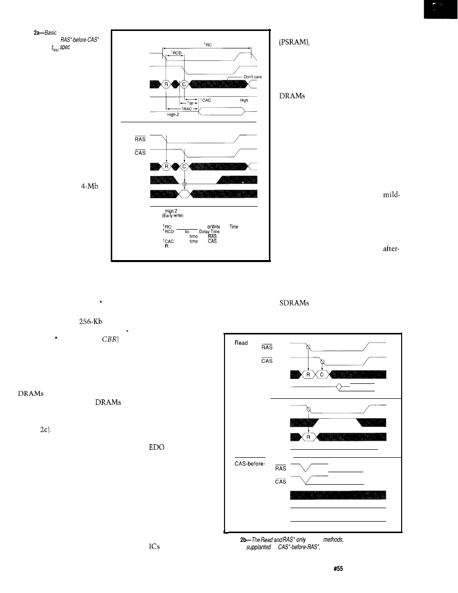
Figure
DRAM read and
write cycles use
a
technique. The
determines
the access speed of the DRAM.
Read cycle
RAS
CAS
Address
W E
Dout
Write cycle
DRAM to be refreshed
hundreds of times per
second, though those
pesky capacitors often
prove surprisingly more
bitworthy than that.
On average, a refresh
cycle needs to occur every
15 us or so (i.e., l-Mb
DRAM needs 5 12 refresh
cycles every 8 ms, a
DRAM requires 1024
cycles every 16 ms, etc.).
But, there’s nothing that
says you can’t group all
your refresh cycles in a
burst.
Figure 2b shows the
popular types of refresh
cycles. The first is simply
to read a location in each row, a
scheme well-suited to graphics
applications or software-refresh
schemes. The similar RAS -only
refresh cycle was the most widely used
on the 16-, 64-, and
DRAM
S
.
Address
WE
Din
Dout
Random Read
Cycle
RAS CAS
‘RAC: Access
from
Access
from
Row Address
C.
Column Address
Starting with 1 -Mb DRAM
S
, CAS
l
before-RAS (also know as
refresh was offered and has since
become popular. With an integrated
refresh-address counter, CBR doesn’t
require an external address.
Address
About the same time as the l-Mb
came into existence, the
formerly simple-minded
started to get brainy with the addition
of high-speed access modes (shown in
Figure
All modes rely on the fact
that once a row is accessed, it’s
possible to access different columns
quickly, without requiring a new
R A S ’ c y c l e .
others, page mode
has proven the
market favorite.
Recently, a variant
of page mode called
Extended Data Out
(EDO) has been
introduced, which
quickens page-mode
cycles by leaving the
output driver on
between CAS *
pulses. It looks like
is going to be
widely adopted,
further cementing
page mode’s position
as the high-speed
access mode of
choice.
Subsequently,
DRAM technology
has migrated into a
faster than page mode. Static-column
mode, as the name implies, offers
speedy SRAM-like access to the
column depending solely on the
address, not CAS’.
Though a little slower than the
RAS-only
refresh
Page
mode repeats only the CAS
l
cycle for each new column address,
cutting access and cycle time nearly in
half. Note that the column address
need not be sequential. Nybble mode
latches four columns for subsequent
access by CAS * Since access is always
RAS refresh
Address
RAM, TV line memory, pseudo-SRAM
and so on. Nevertheless, the
plain old, xl or x4 page-mode DRAM
reigns supreme in the marketplace.
Now, fueled by the insatiable
demand for more bandwidth (for less $,
of course), a whole raft of clever new
are crawling out of the lab.
One particular model appears headed
for success-thanks not only to good
features, but also to the warm, fuzzy
glow multisource standardization
imparts. Say “Hello” to the new kid
on the block, the synchronous DRAM,
otherwise known as SDRAM.
ROCK ‘EM, CLOCK ‘EM
JEDEC (Joint Electron Device
Engineering Council), a formerly
mannered international standards
committee, has emerged as a powerful
force in the memory market.
Originally, they, like many
standards organizations, reacted to
market realities by documenting
the-fact standards. However, as the
demand for standardization has grown,
their mediation and blessing has
become very important. JEDEC played
a major role in making commodity
a reality by forging a peace
agreement between headstrong
contenders.
Dout
RAS
CAS
Address
Dout
Dout
W F
sequential, no column address is
variety of specialized
Figure
refresh
which require an address,
required, making nybble mode even
including video
are
being
by
which doesn’t.
Circuit Cellar INK Issue
February 1995
6 9
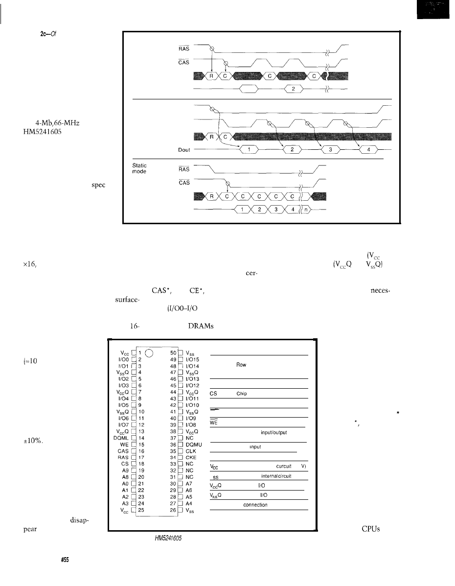
Mb SDRAM) fits in a
footprint about the
same as the old DIP
x 20 mm) and just a
little thicker (1.2 mm)
than a business card.
narrow xl and x4 DRAM
S
. So far, it
finer geometries. In any case, for the
connected together on the PCB
looks like SDRAMs (4 Mb and 16 Mb)
same speed and power reasons,
anyway. The SDRAM features separat
will initially be offered in x4, x8, x9,
whatever the SDRAM connects to is
power for the memory array
and
and x18 configurations. Later, I
increasingly likely to be 3.3 V too.
V,,) and I/O pins
and
to
expect we’ll see (64 Mb) x32.
Otherwise, the pin names
help isolate noise.
SDRAMs reflect the modern
tainly look familiar. There’s RAS*,
DQMU and DQML are individual
downsizing trend in their use of TSOP
WE*,
and multiplexed
byte enables for the data bus,
(Thin Small Outline Package)
addresses just like before. The data
sary to support an atomic, byte-write
mount technology. Thanks to TSOP,
lines
15) are bidirectional,
operation. Otherwise, a byte write
the miniaturization possibilities are
but the separate DIN and DOUT lines
would require a word read, byte mask,
truly impressive--% MB (2 MB for
of the plain
were usually
word write sequence.
It’s the clock pin
(CLK) and its enable
Pin name
Function
(CKE) that are most
AO-A9
Address input
a d d r e s s
AO-A8
important. After all,
Column address
AO-A7
Bank select address A9
that’s what the S in
SDRAM is all about.
11004015 Data-input/output
While a plain DRAM is
select
kind of passive, sitting
RAS
Row address strobe command
around waiting for
CAS
Column address strobe command
someone to tickle RAS
Write enable command
and CAS an SDRAM
DQMU
Upper byte
mask
is a rather nervous
DQML
Lower byte input/output mask
critter that wants to
CLK
Clock
blast some data on
CKE
Clock enable
every clock edge (see
Power for Internal
(3.3
Figure 4). With clock
V
Ground for
rates up to 66 MHz
Power for
pin (3.3 V)
available now and with
Ground for
pin
100 MHz just around
NC
No
the corner, an SDRAM
can handle the data
The easiest way to
move bits faster with
less power is to move
them less far, so
SDRAMs downsize the
power supply to 3.3 V
Now here’s a
place you need to check
an individual SDRAM
data sheet. It looks like
some SDRAMs may
achieve 5-V TTL
compatibility by
tweaking their AC
specs. However, this
capability may
in future-genera-
tion SDRAMs with
(Top View)
rates demanded by
superduper
and
Figure 3-The Hitachi
synchronous DRAM might be considered a New Age DRAM.
gee-whiz graphics.
Figure
the three high-speed
access modes, Fast-Page mode is most
wide/y used.
Fast Page
mode
Address
Let’s start by taking a
look at one of the first
SDRAMs out of the blocks,
the
Hitachi
(see Figure 3).
Thanks to JEDEC standard-
ization, most of the discus-
sion applies to SDRAMs
from other suppliers, though
you’ve always got to be on
the lookout for minor
differences.
The first thing you’ll
notice is it’s wide (x16),
thankfully easing the
frustration caused by the
Dout
Nibble
mode
RAS
C A S
Address
c o l u m n
Address
Dout
70
Issue
February 1995
Circuit Cellar INK
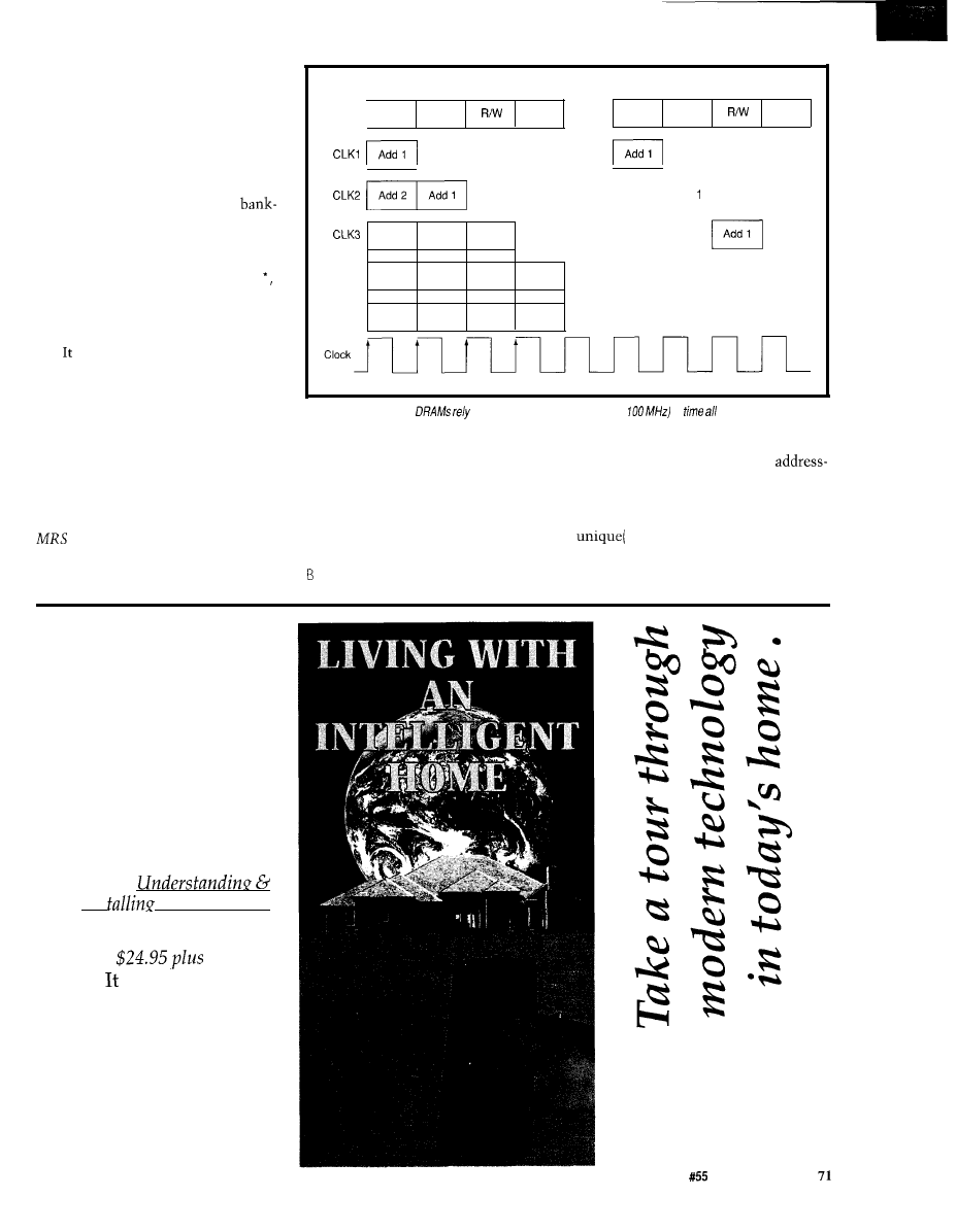
ELECTRONIC BANKING
Looking inside the SDRAM
(Figure 5) reveals differences hidden
behind the familiar-sounding pin
names. The most obvious difference is
that the memory array is split into two
banks (selected using A9). As we’ll see
later, this supports a ping-pong,
switching scheme which maximizes
bandwidth.
The other thing to note is that the
familiar-sounding pin names-RAS
CAS*, WE*, and so on-no longer
actually connect to latches and buffers,
but instead feed a control-logic block.
turns out these pins don’t
actually control the memory transfer
(remember, CLK does that), but should
be interpreted as bits in an opcode as
shown in Figure 6. The pins are
sampled at each CLK cycle and inject a
command into the SDRAM pipeline
unless in a DESL (CS
l
high) or NOP
(RAS’, CAS*, WE* high) state. The
first command to get familiar with is
(Mode Register Set) since it
defines the key SDRAM operating
characteristics (see Figure 7).
Synchronous DRAM (pipeline)
Standard DRAM
Add
Latch
Decode
Output
Add
Latch
Decode
Output
E
l
Add
Add 3
Add 2
Add 1
CLK4
Add 4
Add 3
Add 2
Add 1
El Add 1
CLK5
Add 5
Add 4
Add 3
Add 2
El Add 2
Figure 4-Synchronous
on a high-speed clock (e.g.,
66 or
to
commands and data
transfers.
Burst length
refers to how many
bursts.
Burst type
refers to the
data transfers and clocks are associated
ing order of the burst and is normally
with each READ or W R I T command, the
sequential, unless you’re connected to
choices being 1, 2, 4, 8, and full page
a ‘486 or Pentium, which feature a
(which, in this case, is 256). Shorter
!) interleaved, cache line fill.
bursts end automatically, while the
Write mode
offers the option of
ST command terminates full-page
burst read and write or burst read with
Find out how you can
add intelligence to any
home, at a cost that’s
within your budget.
LIVING WITH AN
INTELLIGENT
HOME
will change the way you live.
Written by David Gaddis,
author of
Ins
Home Sus terns
This VHS video cassette retails
for
$5 s&h.
is being offered to
Circuit Cellar INK
subscribers for only $17.95
plus $4 s&h (U.S.)
ORDER TODAY!
Don‘t let this exciting technology
opportunity puss you by!
l
l
Circuit Cellar, Inc.
4 Park St.
l
Vernon, CT 06066
Tel: (203) 8752752
Fax (203) 872-2204
Circuit Cellar INK Issue
February 1995
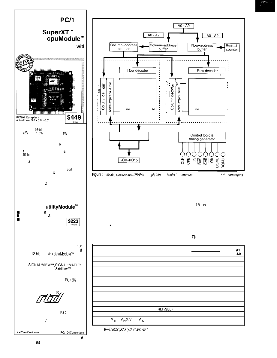
Replace Four
Conventional
04
Modules with
One
CMF8680
Embedded PC/XT Controller
Intelligent Power Management
n PC/XT compatibility with 286 emulation
n 14 MHz,
8086 CPU
n
only;
at 14.3 MHz,
at 7.2 MHz
n Intelligent sleep modes, 0.1 W in Suspend
n ROM-DOS and RTD enhanced BIOS
n Compatible with MS-DOS real-time
operating systems
n M bootable Solid State Disk free software
n
configuration EEPROM (2K for user)
n 2M on-board DRAM
n IDE floppy interfaces
n CGA CRT/LCD controller
n Two RS-232 ports, one RS-485
n Parallel, XT keyboard speaker ports
n Optional X-Y keypad scanning/PCMCIA
interface
n Watchdog timer real-time clock
Expand This Or Any PC/l 04 System
with the
CM106 Super VGA
Controller
Mono/color STN TFT flat panel support
Simultaneous CRT LCD operation
Resolution to 1024 x 768 pixels
n Displays up to 256 colors
Speed Product Development with the
DS8680 Development System
Your
DS8680 includes the CMF8680, CM102
keypad scanning/PCMCIA, CM104 with
85MB hard drive, CM106 SVGA controller
DM5406
100
in an
enclosure with external power supply, 3.5”
floppy, keyboard, keypad, TB50 terminal
board,
MS-DOS, SSD software
for just
$2950.
For more information on our
and
ISA bus products, call today.
Real Time Devices USA
200
Innovation Blvd.
l
Box 906
State College, PA 16803 USA
(814) 234-8087 Fax: (814) 234-5218
RTD Europa
l
RTD Scandinavia
a founder of the
72
Issue February 1995
Circuit Cellar INK
Memory array
Memory array
Bank 0
Bank 1
512
X 256 column X 16
512
X 256 column X 16 bit
Input
Output
buffer
buffer
are
two
for
performance. Many or me
have familiar names, but now, they are little more than the opcodes for an on-chip logic that controls the actual
memory access.
single write. The latter mode may be
rates demanding more delay. For
useful in graphics applications (e.g., a
instance, a particular-speed SDRAM
burst read refreshing the CRT and
may achieve
clock cycle and
single writes coming from the drawing
access times with CAS* latency 2, but
processor) or to support a CPU with
only 30 ns with CAS* latency 1. Figure
write-through cache.
8 summarizes the CAS
l
latency and
CAS latency depends on how
burst-length options.
many clock cycles elapse between a
As shown, a transfer is initiated
request and transfer, with higher clock
with an
A C
(activate) command,
CKE
Function
Symbol
n - l n
CS RAS CAS WE A9 A8
Ignore command
DESL
H
X
H
X
X
x x x x
No operation
NOP
H
X
L
H
H
H X X X
Burst stop in full page
BST
H
X
L
H
H
L
x x x
Column address and read command
READ
H
X
L
H
L
H V L V
Read with auto-precharge
READ A
H X L H L
H V H V
Column address and write command
WRIT
H
X
L
H
L
L v L v
Write with auto-precharge
WRIT
A
H X L H L L
V H V
Row address strobe and bank act
ACTV
H
X
L
L
H
H V V V
Precharge select bank
PRE
H
X
L
L
H
L v L x
Precharge all bank
PALL
HX L L H
L X H X
Refresh
H V L L L
H X X X
Mode register set
MRS
H
X
L
L
L
L
L
L
V
Note: H:
L:
or
V: Valid address input
Figure
pins encode the synchronous DRAM instruction set.
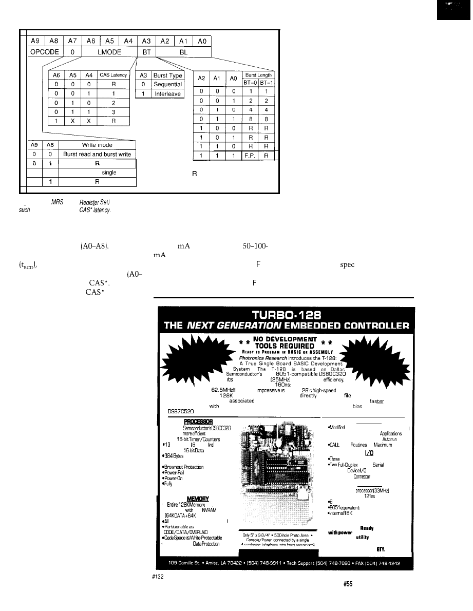
1 0
Burst read and
write
F.P. = Full Page (256)
is Reserved (inhibit)
1
Figure 7-The
(Mode
command defines synchronous DRAM basic operating characteristics
as burst length and
which is pretty much like the RAS*
cycle of old. In this case, it selects the
bank (A9) and row
This is
followed, after the requisite delay
by a READ or WRIT command
that specifies the column address
A7) as in yesteryear’s
After the
previously specified
latency, the
data is blasted on each clock edge.
The READ A, WRIT A, PRE, and
PALL commands all have to do with
precharge. Since precharge has been
automatic since the days of the 2116,
it might seem like a step backward to
make the system designer handle it.
Fortunately, if you’d rather not be
bothered, the A versions of the READ
and WRIT commands feature auto-
matic precharge. However, as in plain
DRAM, automatic precharge lengthens
the basic cycle time. Fortunately, overt
control of precharge in conjunction
with the bank scheme does offer the
opportunity for aggressive designers to
hide precharge in one bank while
transferring data from another.
That about covers the SDRAM
instruction set, except for our old
friend refresh, of which two variants
are offered, depending on the state of
the CKE pin. If CKE is high (i.e., the
clock is enabled), an AUTO REFRESH
mimics a plain DRAM’s CBR-refresh
cycle (i.e., an on-chip refresh counter
means no external address is required).
SELF REFRESH (CKE low) is kind
of a power-down mode, in which the
DRAM keeps itself refreshed while
consuming amazingly little power
(only 2
compared to its
active consumption). It’s tempting
to just leave the SDRAM in SE L
R E FRESH between accesses. Unfortu-
nately, however, exit from SE L
R E FRESH requires the issuance of 1024
cycles of AUTO REFRESH
to
update the
refresh counter, so SE L F R E FRESH is
only suitable for serious napping.
Figure 9, showing the allowed
instruction sequences, looks compli-
cated, but really isn’t if you talk it
through. When idle, the SDRAM
should be refreshed 1024 cycles every
16 ms. An ACTV command (think of it
as a RAS * cycle) selects a bank and
row for action. Once activated, the row
can be accessed freely, bursting data
both ways from random column
addresses. After all transfers are
completed (or if the row address
changes], exit is via a precharge cycle,
taking the SDRAM back to the idle
and refresh state.
Remember, the key point of the
two-bank scheme is that each bank
can be in a different state and the state
transition intervals are faster between,
rather than within, banks. For in-
stance, the minimum ACTV-to-ACTV
(i.e., cycle time]
within a bank is
110 ns while between banks it’s only
30 ns.
new
With
2X clock speed
and 3X cycle
an
instruction can execute in
an 8051 equivalent speed
of
Equally
the T-l
NVRAM
Interface. Any of the
RAM may be programmed
from a PC
through the console:
eliminating EPROMs and
tools
Program Development has never been
or more
convenient, even
the finest EPROM emulator The T-l 28 features PORT 0
and EA-select for
upgrade.
l
Oallas
l
30C%
than the 8051
*Three
Interrupts Ext. 7
*A second
Pointer
of Internal RAM
*Programmable Watchdog
Reset/Interrupt
Reset
BASIC520
BASIC-52 Interpreter [BASIC-520:
Now Fast Enough for New
*Stack BASIC Programs and
ASM
for
Speed
S-bit Parallel Ports
RS232
Ports
*Decoded
Strobes
l
5w?n Bus
supported by Franklin C51
l
Mao
populated
fast
CODE]
memory pmgrammed on-board
l
SatwfdleArt
UPGRADE
l
0S87C520
l
lnstruc00n cycle:
25 MIPS
82 5 MHz
ROM/l K SRAM
Comes
to Run
adapter/cable assembly.
Includes
diskette with
DETAILED TECHNICAL MANUAL
$199
in
Circuit Cellar INK Issue
February 1995
7 3
CAS Latency
CLK
Command
Active
Address
Row
Read
CL: CAS Latency
Burst Length = 4
Burst Length
CLK
Command
Address
BL = full
(256)
6
7
out 6
7
BL Burst Length
CAS Latency 2
Figure
not shown on figure, remember that higher
latency offers a faster clock
Short-burst transfers automatically terminate,
but full-page bursts
be explicitly terminated
the J command.
Issue
February 1995
Circuit Cellar INK
Connect via ROM Socket; DIP; PLCC; SMT
Emulate ROMs up to
in Size
Fastest Downloads Available:
Parallel; Serial; Ethernet
Run Industry Standard Debuggers
Target Processor Independent
Support
Targets
Host Software Sources Included
Shielded Cables for Reliable Operation
Money-Back Guarantee;
Year Warranty!
Unlimited Phone Support; 24hr BBS
Call Today 1
(1
n
800=776=6423)
Grammar Engine Inc.
921
Dr., Suite 122
l
Westerville, OH 43081
l
Fax
7
‘AD \
Automatic
after
of command
resulting from command input
Figure
synchronous
DRAM is
either idle or
reading and writing or
BURST OR BUST
You might think all this
and
talk implies some kind of
lo-times breakthrough in DRAM cell
speed. In fact, the speed of basic
memory operation really isn’t much
different (witness the 1
cycle
time mentioned above is about the
same as plain DRAM
S
). The SDRAM
simply blazes a faster trail to what’s
otherwise regular DRAM.
Thanks to the ping-pong feature,
even the simplest SDRAM setup
latency = 1, burst length = 1)
offers good potential. Note that the
parallelism can be extended across
multiple SDRAMs as well (i.e., you
can also ping pong between chips).
However, there’s no doubt that
bursty applications such as high-end,
32-bit
and graphics best match
the features of SDRAM. The tradeoff
between CAS
l
latency, clock rate,
burst length, number of chips, and so
on is hard to generalize.
Graphics applications will likely
shoot for maximum bandwidth (e.g.,
length = 3, burst length = full
page, CLK = 66 MHz). It then becomes
simply a matter of choosing the
number of SDRAMs to support a given
display. For example, a 1024 x 768 x 24
x
display calls for 170 MB per
second, while each 66-MHz SDRAM
offers 132 MB per second. Thus, a
SDRAM frame buffer easily handles
display refresh, leaving about 40%
bandwidth for drawing.
CPU main-memory applications
are a little more tricky. A simple
controller may just set the burst length
equal to the cache-block-refill size and
leave it at that. CAS
l
latency versus
CLK rate largely depends on
controller speed, cost and complexity
issues, and “hit ratio” tradeoffs (i.e.,
weighing greater latency penalty
against higher burst bandwidth).
More aggressive controller designs
are possible if you’re willing to sift
through the entrails of your program
and truly understand its behavior. It
might be wise to put instructions and
data in separate SDRAMs to take
advantage of locality. Often, instruc-
tion- and data-cache-refill sizes are
different, so each
burst
length could be set appropriately.
Another idea is to control burst
length dynamically, either by overtly
terminating full-page bursts or by
reprogramming the mode register. This
opens the door to really clever dy-
namic or “greedy” burst schemes,
which wring all possible bandwidth
out of the SDRAM.
No doubt, the prospect of rolling
your own SDRAM controller, espe-
cially a fancy one, is rather daunting.
The good news is I expect SDRAM
support will quickly migrate into
likely partners including
RISC
graphics
and PC chipsets.
Tom
has been an engineer in
Silicon Valley for more than ten years
working on chip, board, and systems
design and marketing. He can be
reached at (510) 657-0264 or by fax at
(510) 657-5441.
Hitachi America, Ltd.
Semiconductor and IC Division
2000 Sierra Point Parkway
Brisbane, CA 94005 18 19
(415) 589-8300
Fax: (415)
422 Very Useful
423 Moderately Useful
424 Not Useful
Circuit Cellar INK Issue
February 1995
7 5
Downsizing
John Dybowski
1
Flash-based
Microcontroller
I would never
someday I’d be a proponent of the 805
architecture. But, in light of the work
I’ve been doing lately with a variety of
805 1 derivatives, this must be exactly
the way I’m coming across. Quite
frankly, I’m not entirely comfortable
with the situation.
I still remember my first encoun-
ter with the 805 I immediately
recognized its utility as a Boolean
processor and was quite impressed
with the ease with which it handled
bit-oriented I/O. At the same time, I
was appalled by the seemingly random
architecture and the absence of some
rather fundamental instructions.
These idiosyncrasies continue to irk
me and appear all the more enigmatic
in light of recent microcontroller
advances.
Still, it pays to remember that
silicon was a much more precious
commodity at the time the 805 1 was
developed than it is today. Obviously,
the seemingly arbitrary exceptions and
bizarre architectural quirks were the
result of gut-wrenching decisions
made to bring the processor’s principal
features in line with a constrained
silicon budget. It’s not an uncommon
problem. I’m sure the consequences of
those unpleasant decisions were not
taken lightly.
Although the mechanics of
crafting silicon have changed, the
fundamental aspects of doing business
remain the same. And, this is the key
to the puzzle since this is, after all, a
business venture and not a science fair
project. As a case in point, consider
how this same scenario has replayed
over the years.
More recently, the same tough
choice between price, performance,
and features was played out with yet
another strange, but extremely
successful microcontroller-the much
maligned, Microchip PIC
To
me, this processor is the epitome of
business sense winning out over
technological constraints.
The thing doesn’t even have an
interrupt. Although technically a
brainer, adding an interrupt would
have resulted in totally blowing the
target price. Talk about tough choices.
As it turned out, the chip’s many
deficiencies were each countered by a
combination of skillful marketing and
imaginative technical support. They
even convinced a sufficiently large
number of engineers that they really
didn’t need that interrupt after all!
Both the 8051 and the
architectures have established them-
selves in their respective spheres of
application. As Microchip develops the
PIC series into larger, more capable
devices, it’s inevitable that the
architecture’s basic simplicity has
become somewhat obscure.
Ironically, the
big
brothers are starting to look a lot like
803 1 s, a rather questionable distinc-
tion. It’s also a dubious arena to
compete in since it is well-served by
some firmly established controllers.
To me, the original
is still the
soul of the PIC family. Warts and all,
this is the part I turn to when I need to
implement bare-bones functionality
and all I can afford is a $2 chip.
WRAP IT UP
Formerly, using a higher-level
language on 805 1 -class processors was
considered a disputable practice at
best. After all, the basic architecture
has little enough real stack space to
begin with and no stack manipulation
capability at all-obviously, a major
drawback with a stack-oriented
language. Combining these handicaps
with a meager instruction set and all
those overlapping code, data, and bit
segments, it’s no wonder that many
viewed using code generators on such
micros as nothing more than an
76
Issue
February 1995
Circuit Cellar INK
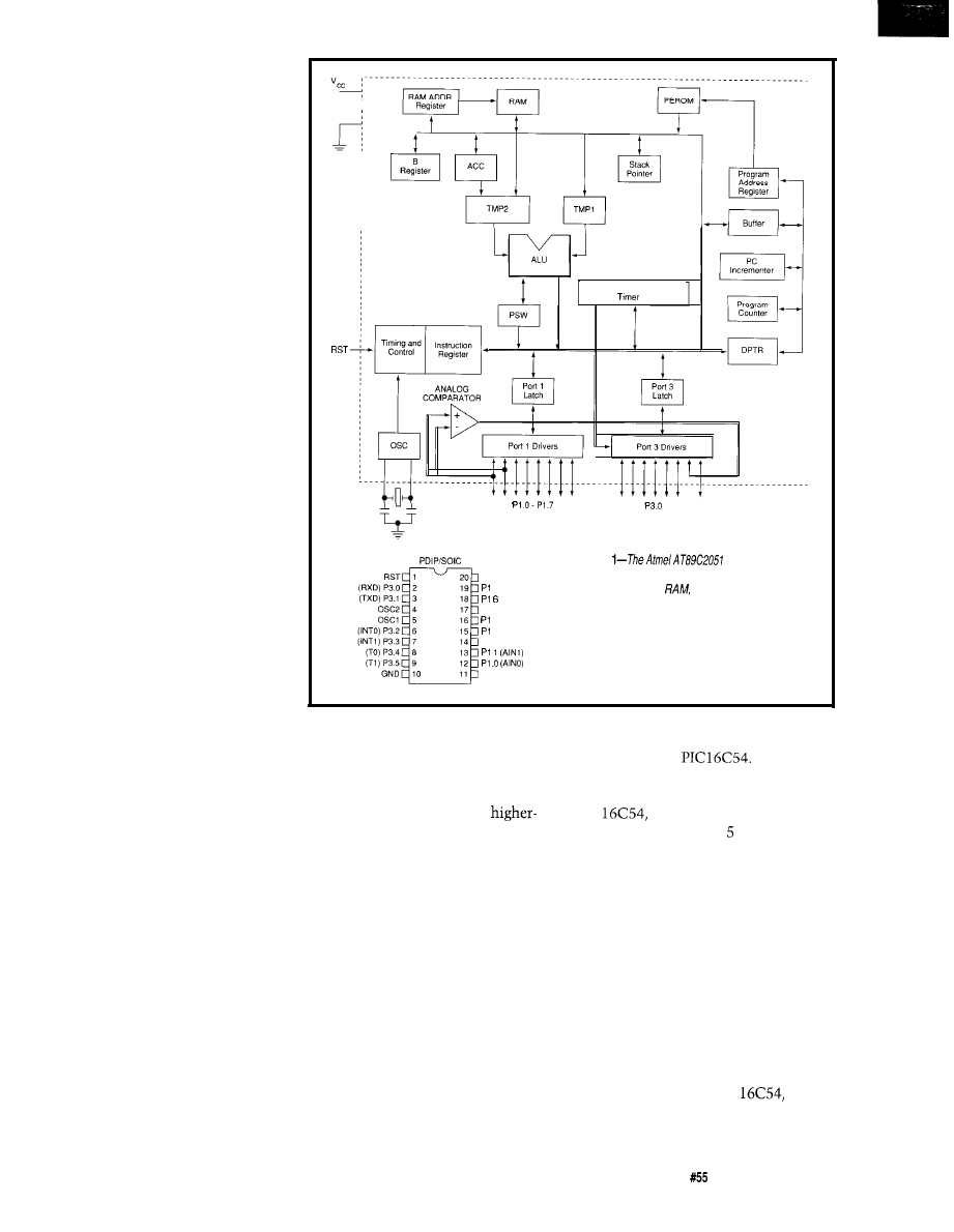
interesting diversion with little
practical consequence.
Evidently, in spite of these
obstacles, compiler developers have
managed to prevail. Actually, it could
be argued that it is because of these
obstacles that they have been so
successful. The fact is, placing a good
code generator between such an
architecture and yourself isn’t that bad
an idea. When I’m writing code, I don’t
mind dropping to the machine level
when it’s necessary or expeditious. I’m
also well aware of how counterproduc-
tive it is to remain at that level any
longer than necessary.
An analyses of the situation
reveals that some of the most popular
embedded-C compiler implementa-
tions run on some of the more “diffi-
cult” processors. This could be
construed as something of a paradox.
The implication seems to be that these
popular, although irregular, processors
assume a level of anonymity through
the insulating effect of the language
compilers.
From this, it follows that selecting
an appropriate architecture should be a
relatively straightforward and rational
exercise. This might be true if a typical
embedded program could be coded
entirely using a higher-level language.
That this is not the case, especially
with 8-bit processors, is evident by the
continued popularity of older architec-
tures like the ones I’ve been describ-
ing-so much for rational thinking. If
it looks to you like a case of the tail
wagging the dog, then you’re not
alone.
The fact is, as any embedded
developer well understands, portable
code is something that is extremely
elusive and difficult to accomplish in
most embedded applications. Usually,
system I/O turns out to be such a big
part of the overall picture that it is the
primary concern.
And, regardless of “proper” coding
techniques, embedded programs are
often laced with timing dependencies
that rely on the execution times of
various pieces of code. When doing
this type of programming, the bottom
line is that you have to know when to
get down to the machine level and you
must have a good understanding of the
GND
Interrupt. Serial Port.
and
Blocks
P3 5
vcc
7
P I . 5
4
3
P I . 2
P3.7
Figure
preserves
much of the original 8051 core, but adds f/ash
memory and more
plus is squeezed in a
smaller package.
quality of code your compiler is
generating.
Still, in spite of all the complicat-
ing issues, the productivity gains that
can be realized from using a
level language offer a compelling
incentive to rethink the way you’ve
been writing your embedded programs.
the more limited controllers and
processors.
Recently, some of the most
difficult C implementations have been
The benefits of using language
compilers can be perceived differently
depending on your particular needs.
Minimally, an efficient compiler can
function as a sort of stylized assem-
bler. This is especially true of the C
programming language which affords
excellent control of low-level func-
tions. The incentive for this category
of usage is pretty strong with many of
realized on resource-starved control-
lers such as the
Frankly,
when I first found out that engineers
were actually seeking C compilers for
the
I was a bit baffled. I mean,
with a two-level stack, 12 words of
program memory, and a few dozen
bytes of read/write storage, it didn’t
exactly seem like a good fit. It looked
like the compiler’s overhead alone
could swamp the processor’s meager
resources.
tried one yet but, having done a couple
of projects involving the
I’m
very interested. You see, one of the big
attractions of a language compiler for
It turns out that there are some
very smart software people and now
there are a number of C compilers
available for these minuscule proces-
sors. Reports from the field indicate
that this stuff really works. I haven’t
Circuit Cellar INK Issue
February 1995
7 7
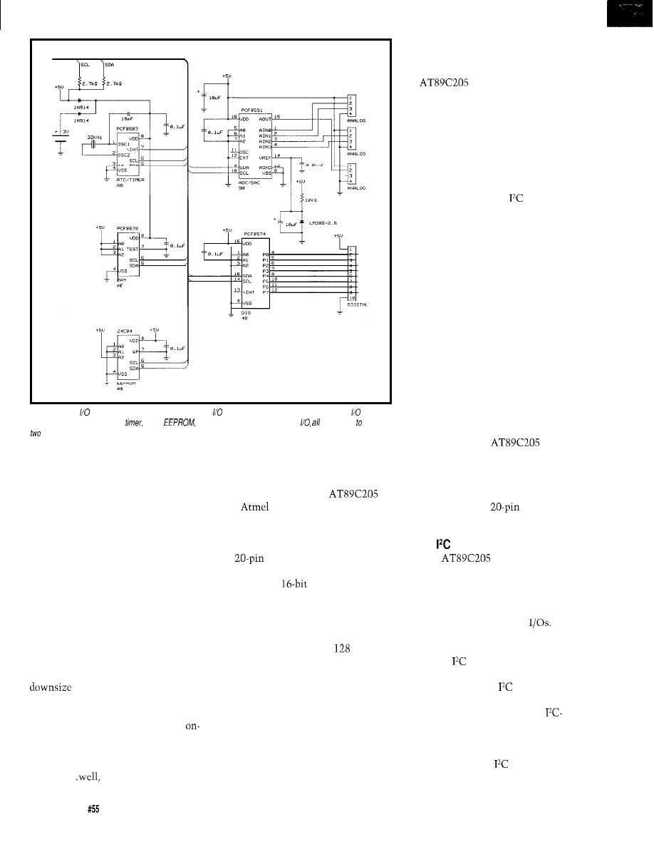
H O S T P R O C E S S O R
Figure Pa-Host bits are preserved by connecting most devices to a single pair of PC lines. The board
includes a real-time clock and
RAM,
analog in, analog out, and digital
connected just
wires.
me is its ability to handle many of the
tedious programming details. And,
there are many of these indeed when
working with very small processors.
Put another way-if it’s ugly, wrap
it up!
LISTEN TO YOUR CUSTOMERS
There’s also been a trend to
Recent evolutionary trends have
involved enhancing “standard”
the architecture. Downsizing
processor architectures. For better or
worse, the 805 1 is now perceived as
has led to a loss of some capabilities, a
standard indeed. In recent columns,
I’ve shown how this basic architecture
reorganization of the fundamental
has gained in performance and capabil-
processing core, and a reduction of
ity while retaining its standard
footprint and pinning.
chip memory. The high end has been
well served by a variety of capable
derivatives. The low end until recently
has been..
the low end. But
finally, someone has introduced a very
small 805 1 that doesn’t give up any of
its fundamental features.
It may not seem like a big deal at
first, but it is the inclusion of the full
The new, flash-based
1
from
is a welcome addition to
the 8051 family. More than just
128 bytes of internal RAM that opens
another scaled down 805 1, this
processor is a full-blown 805 1 housed
up substantial opportunities for using
in a
package. All the standard
this part with standard commercial C
805 1 peripherals have been retained
including two
timers along with
their gating controls and associated
compilers. While using a compiled
interrupts, two external interrupts, and
a full-duplex hardware UART. This is
language is certainly an option with
in addition to 2 KB of flash program
memory and the standard
bytes of
some of the more restricted 805 1
internal RAM.
derivatives, things naturally get quite
limited with the 64 bytes of RAM
most of these smaller chips offer. And,
if you’re worried about code efficiency,
the
1 specifies an operating
frequency from DC to 24 MHz. This
gives you the elbow room to handle
any reduction of efficiency that results
from using a code compiler.
Another area that competitive
products have consistently ignored is
the inclusion of a hardware UART.
Although many of the competing parts
offer hardware-assisted
interfaces,
it’s obviously of little consolation
when you have to provide for standard
asynchronous communications.
From where I sit, the outcry for a
hardware UART has been long, loud,
and clear. Needless to say, thus far, the
semiconductor manufacturers have
been totally unreceptive to what users
have been calling for. Their response
to these requests has simply been to
either say that you really don’t need it
or to suggest running one entirely in
firmware. I’m surprised this “what
we’ve got is what you need” mentality
has prevailed as long as it has.
As a result of this attitude,
manufacturers have left themselves
wide open, jeopardizing a significant
market share. If the
1
offered nothing more than just a
hardware UART, its success would be
ensured. The fact is it’s got a lot more
than that going for it. Figure 1 shows
the contents of this
processor in
block form.
I LIKE
The
1 possesses a full
805 1 architecture, it just happens to
have fewer I/O pins. Obviously, to
design a general-purpose embedded
computer around such a device, it’s
necessary to conserve these
The
most efficient way to hook up a lot of
peripherals using just a couple of lines
is over the
bus.
At first, it might seem that not
having any hardware
support
might prove to be a major liability in
what essentially amounts to an
based computer. But, with the excep-
tion of some very specialized applica-
tions, it is not a problem at all.
Remember that
defines a
synchronous protocol that is capable of
78
Issue
February 1995
Circuit Cellar INK
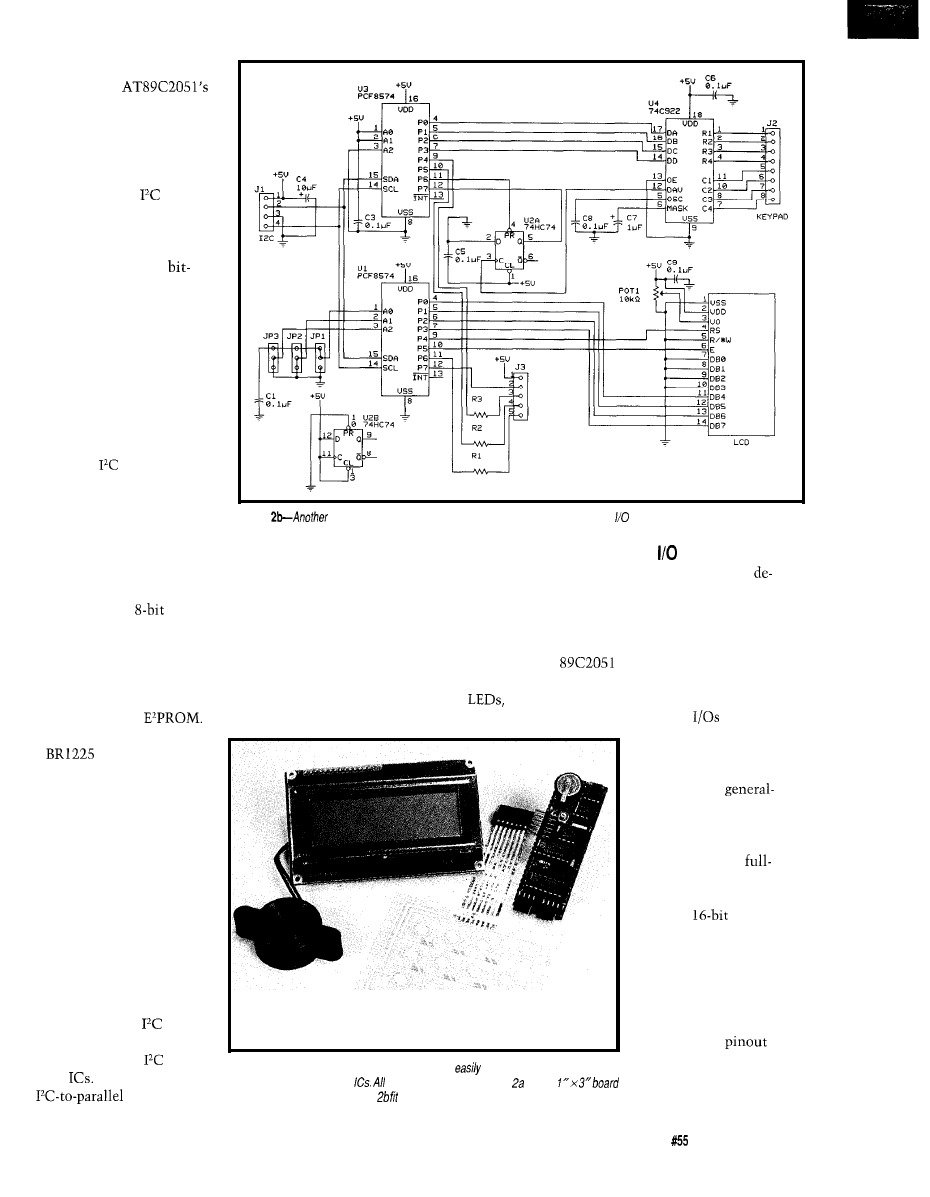
running all the way down to
DC. With the
complement of internal and
external interrupts, it’s easy
to arrange time-critical
processes to run entirely
under interrupts. This lets
you bit-bang the
and still
stay live to service your real-
time operations.
Obviously, this is luxury
you don’t have when
widdling asynchronous
communications, which by
definition must adhere to
relatively strict timing
constraints. Sure, you can
run asynchronous communi-
cations in the interrupts, but
there are serious limitations
to the maximum bit rate you
can reach.
Some
peripherals
come prepackaged and ready
to go. The small multifunc-
tion card shown in Photo 1
illustrates a number of such
Figure
interface board handles a 4 x 20 LCD, 4 x 4 keypad, and general over two wires.
useful functions. Figure 2 depicts the
and some support logic, a 4 x 20 LCD
PROCESSOR
card’s schematic. The I/O-related
functions include four single-ended or
two differential
analog inputs,
one 8-bit analog output, and eight
and a 4 x 4 keypad can be supported
So far, the I/O devices I’ve
using the same two I/O lines. The
scribed encompass all the peripheral
control card for this peripheral system
functions a very small embedded
attaches almost invisibly beneath the
computer might need. The beauty of
digital I/O points.
standard 4 x 20 supertwist LCD panel
this arrangement is that, although the
The card also provides a real-time
as shown in Photo 2. This arrangement
has only 15 I/O pins to begin
clock-calendar timer with 256 bytes of
leaves a number of general-purpose I/O
with, after accommodating all these
RAM, a dedicated 256 bytes of RAM,
lines free to drive a beeper,
and
functions we are still left with I3 for
and 5 12 bytes of
The RTC
other indicators.
general usage. These
can be
and RAM are backed using
a
lithium coin cell
that is also contained on
the card. The card, includ-
ing connectors, measures
only 1” x 3”. If your applica-
tion doesn’t need these
functions, then simply
don’t load the card. PC,
especially a firmware-based
implementation as used
here, carries very little
hardware overhead. Even
the requisite pull-up
resistors are located on the
card.
Higher-level
functions are realized using
a combination of
and
logic
Using a couple of
converters
Photo 1-A sample of the peripherals which can be
hooked up using a
combination of PC and logic
the devices shown in Figure fit on a
(upper right) while those in Figure under the LCD display.
Although the on-chip
I/O lines are for the most
part 805 1 compatible,
there are some important
differences. Refer again to
Figure 1. You can see the
familiar 805 1
nomenclature has been
preserved. From this
figure, you can also see
Circuit Cellar INK
Issue
February 1995
directly tested and set by
the processor and are
therefore very fast.
Among these
purpose I/O bits are two
external interrupts,
receive-and-transmit
connections to a
duplex UART, and the
gating signals for the two
internal
timers.
7 9
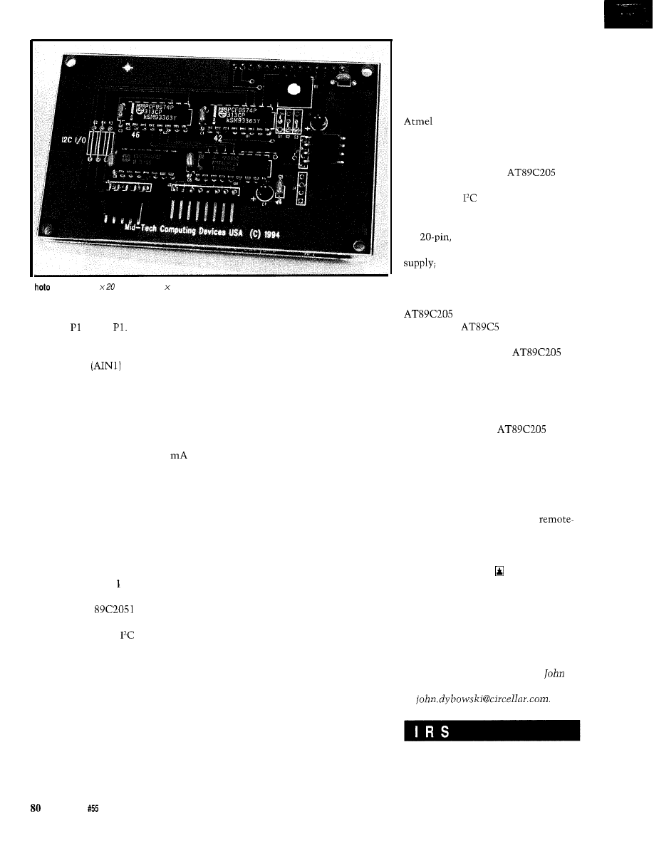
2-A standard 4 LCD display, 4 4 keypad, and PC interface are supported on a board that mounts on
the back of the display.
that pins .O and
1
are designated
as analog inputs. These high-imped-
ance inputs serve as positive (AINO)
and negative
inputs to the
built-in precision analog comparator.
P3.6 is not available externally and
instead takes the output of this
comparator as its input. To facilitate
interfacing to real-world loads without
the need for external buffers, ports
1
and 3 are rated to sink a full 20
when running at 5 V.
MAKE SENSE?
If you accept that the peripheral
mix I’ve described for my system is
not unusual, then perhaps I can offer
some insight from my own experi-
ences on issues like code portability,
code reuse, and the enduring success
enjoyed by the 805 architecture. In
this context, I will also elaborate on
why I feel the
is such a
significant processor.
Simply put, the
peripheral set
I’ve described has served me well in a
variety of configurations on a variety
of host systems for a number of years.
I’ve developed a fair amount of C code
to support these functions, but the
main low-level drivers are all, of
necessity, written in hand-tweaked
assembler.
This in itself represents a signifi-
cant investment of time and effort. To
this, of course, you must add the
Issue
February 1995
Circuit Cellar INK
“standard” overhead of the trade. This
overhead includes such things as
interfacing low-level code to the
compiled code (usually quite different
for each compiler you use); debugging,
testing, and validating functions;
documentation; and continuing
support. Underestimating these
associated tasks can have a deleterious
effect on your continued success in
this field!
Electronics means different things
to different people. To those of us that
have bills to pay, it’s a business. In this
context, the bottom line revolves
around spinning off applications.
Efficiency in doing so is what can
make or break it. Sure I could code up
a new set of low-level drivers for a
different processor in a relatively short
period (disregarding the overhead of
course). And, if I had to, I could take
all that C code and rewrite it in
assembler if the processor I was using
didn’t have the horsepower to handle a
compiled language.
Individually, these are fairly small
tasks. It’s only when you look at the
overall picture that it becomes evident
that a significant amount of time can
be spent on these tasks. And, I haven’t
even touched on things like regenerat-
ing all my interrupt-driven communi-
cation routines, timer-capture func-
tions, and the like. There comes a
point when you have to ask yourself
where you want (or can afford) to
spend your development time.
EMBEDDED TOOLS
I’m sure it’s obvious I have more
than just a passing interest in the new
processor. Next month, I’ll cut
through the fluff and devote my
attention to the design and develop-
ment of a very small, general-purpose
computer based on the
1.
Having defined the 1” x 3” form
factor for the
peripheral card, I will
use the same footprint for the main
processor card. This card will contain
the
flash-based processor; an
RS-232 and RS-485 interface; power
and prototype area.
The main focus of my column,
however, will be the associated
development system for the
1.
In this respect, I’ll also be
covering the
1
flash-based
processor that, with some hardware
assistance, emulates the
1.
The system works with a variety of
target systems since it uses a standard
umbilical cable hookup.
Of course, once you get an
application up and running, you’ll
want to program the
1
flash
memory. This will be accomplished
with the built-in flash programmer
contained right on the development
system. As usual, I’ll be calling on my
esteemed colleague, Dave Dunfield, for
his fine PC-hosted development tools.
I’ll be using his simulator and
debugging software to round out the
development system. For code genera-
tion, I plan to use his Micro-C and
assembler products.
John Dyhowski is an engineer in-
volved in the design and manufacture
of embedded controllers and commu-
nications equipment with a special
focus on portable and battery-oper-
ated instruments. He is also owner of
Mid-Tech Computing Devices.
may be reached at (203) 684-2442 or
at
425 Very Useful
426 Moderately Useful
427 Not Useful

The Circuit Cellar BBS
bps
24 hours/7 days a week
(203)
incoming lines
Internet E-mail:
We’re going to stray a from hard-core electronics
month
enter the more physical world. In the first thread, we look at cab/e
impedances, connectors, and fermination. The topic can be
something of a black art at higher frequencies.
In our only other thread, we look at some suggestions for
running a three-phase motor on single-phase power. The ideas run
the gamut of implementation complexity, and is a fun discussion
to read through.
Keep an eye out next month for the next version of TBBS (2.3).
promises to overhaul the file area support, plus adds some nice,
small enhancements throughout the rest of the system. you
more once we have if up and running.
Cable termination
5925
From: DAN HOPPING To: ALL USERS
Not being the video analogical type, I have a couple of
questions on the subject of video impedance and termina-
tion. I have a fancy video edit control system that brings the
video in from two player decks and outputs the mixed
signals and effects to the record deck. I have discovered that
there are short (less than 12”)
coax cables that bring
the video signals into the PC and back out.
My questions are: Would this short length of
cable make a difference to the video signal that, as I
understand it, should be terminated with 75 ohms?
What does it mean to have a
cable versus a
ohm cable? Are there different BNC connectors for
versus
cables? What does impedance mismatching
actually do to the signal?
5967
From: LEE STOLLER To: DAN HOPPING
A
cable is standard for video signals. The BNC
connector you use is determined by the actual cable type.
For runs that are not very long, cheap RG-59U cable works
out well enough, and there are
designed to mate with
it. For long runs in professional installations, type 724 cable
is often used. This is much thicker, and requires
designed for it. The cables going to the editor will probably
be terminated inside the editor. If there are two BNC jacks
for each cable, and there is no termination switch on the
82
Issue
February 1995
Circuit Cellar INK
editor, connect the cable to one jack, and then connect a
“75-ohm BNC termination” to the other. There is a similar
situation at the input to the record machine.
If, as you say, a cable takes video both to and from the
PC, the PC connection is a “loop-through,” and the neces-
sary termination would be located at the other end of the
“from” cable.
5933
From: RUSS
To: DAN HOPPING
The impedance of a cable (any cable, coax or otherwise)
represents its properties in propagating a wave down it.
Unlike DC signals, you must take this into account when
sending high-frequency signals down a cable.
Consider a line terminated in a variable resistance at its
far end. First take the two extremes of an open circuit and a
short circuit. With an open, there can be no current flowing
at the far end (no path for it to flow), but voltage can be
present. With a short, there can be no voltage developed at
the end, but current can flow. Impedance is the ratio of
voltage to current anywhere on the line.
If a voltage (or current] wave is propagating down a line
and sees the open or short, interesting things will happen.
In order to meet this “boundary condition,” a reflected
wave of suitable voltage/current magnitude will be created.
This wave will propagate back down the line from the far
end to the sending end, and will vectorially add to the wave
going in the other direction.
Recall that this propagation takes place at nearly the
speed of light, just a bit less depending on the “propagation
velocity” of the cable (often in the
range). This too
depends upon the cable’s physical properties such as
conductor size, spacing, and dielectric constant of the
insulation. The fact that the wave does not propagate
instantaneously
is why all these considerations are neces-
sary. For DC or very low frequencies, the propagation time
(on most length cables) is very short compared to a wave-
length of the signal. That’s not true at higher frequencies.
Returning to the open/short condition, what effect that
sort of termination has at the sending end (which is often
where you are most concerned) depends on the electrical
length (in wavelengths) of the line. For example, an “open”
placed any odd quarter wavelengths away from the sending
end will actually look like a short, while a “short” will look

like an open! Interesting, huh? At multiples of a half
wavelength, the load will reflect back looking exactly like
what it truly is. At in-between wavelengths it can look
capacitive or inductive. Life gets interesting!
When a wave propagating down a line sees a load equal
to its characteristic impedance, the voltage/current (hence
impedance) relationship all along the line is satisfied when
the wave reaches the far end. Thus the signal “sees” a line
that (electrically) appears to go on forever and ever! This is
what’s referred to as “matching impedances” and why a
ohm video source usually is sent over a cable with 75-ohm
characteristic impedance and is terminated in a 75-ohm
load. Ditto for
source,
TV twin-lead, or
even
twisted pair used in, say, RS-485.
What effect will a short cable of different impedance
have? It depends on the frequency (wavelength) of the
signal. For your video example, using a short
cable
of a few feet will usually have no effect. Same goes for
connectors.
The physical “length” of a connector is quite small, so
using the “wrong impedance connector” only becomes a
problem when that length is a substantial portion of a
wavelength. In practice, this means above 100 MHz or so.
Any BNC connector will suffice for
systems
below that frequency. But there
are
both
and
(with slightly different physical dimensions, usually
of the center pin area) for precise matching. You don’t have
to worry about it in your case.
Often, video equipment (such as monitors, etc.) include
a switch which permits the
terminating resistor to
be switched in or out. If you multidrop more than one
device on the cable, you want only the last or end device to
have the terminating resistor present (per the above discus-
sion), while the others operate in “high-impedance” mode
and have little effect on the signal as it passes by. Again,
same is true with RS-485 multidrop communication.
6037
From: DAN HOPPING To: RUSS
Thanks for your wonderfully detailed reply. Your
explanation helped a lot! I usually get a little lost before
I
see the entire picture because I really like to understand.
Let me put this in terms a digital guy can understand and
you tell me if I’ve missed it. I understand the process of
terminating an address line on a digital board to reduce
reflections and ground bounce. The same holds true for
local area networks and RS-485 communications. So, does
the following make sense?
The whole deal with impedance matching is to provide
a signal path that will not cause reflected waves from an
earlier signal to either attenuate or reinforce the actual
signal as it reaches a device in the signal path.
Assuming the previous to be true. If you had a video
transmitter at the start of the cable and a video monitor
(receiver] at the end of the cable, why couldn’t you just use
any shielded cable and terminate the line at the receiver
with a
resistor? Would the terminating resistor not
eliminate to ground any reflectable portion of the remaining
signal or must the entire length of the cable (assuming its
length is significant compared to the wavelength of the
signal) have the characteristic impedance to properly
eliminate the reflection? Finally, is there anything more
than reflected interference to be considered (assuming the
cable can handle the power)?
Msg#: 6057
From: RUSS
To: DAN HOPPING
Dan, you’ve pretty much got it. Yes, it’s precisely the
same as terminating address lines or RS-485 buses. By the
way, the same holds true for any wave propagation situa-
tion, not only electrical waves-acoustic, thermal, optical,
and so forth. But keep in mind that the medium (cable or air
or water or whatever) always has a characteristic impedance
of its own. If you match the transmitter and receiver to this
characteristic impedance, then there are no reflections in
the system.
So, your example of a video source (with
output impedance] connected to a video receiver (high
impedance) swamped by a 75-ohm terminating resistor is
quite correct. But, the cable that connects the two should
also have
characteristic impedance for everything
to match. If the run is very short (compared to a wave-
length] then there are still reflections, but they occur in a
very brief time, usually much less than any frequencies of
interest, and are essentially filtered out.
I might point out, this “wave mechanism” exists for
DC signals too. If you send a step function from a signal
generator (battery and “clean” switch) with a sending
impedance equal to the characteristic impedance of the
line, you can observe some interesting effects on a fast
scope as you vary the terminating impedance. The voltage
will propagate down the line, hit the mismatch, cause a
reflection, come back and vectorially add to the outgoing
wave, and repeat this over and over, creating interesting
patterns. Often this is taken to be the “ringing” people see
on digital signals (e.g., address lines) and is why termina-
tions and even “transmission line” circuit traces are used
with fast ECL logic, for example.
Another interesting property of impedance matching,
while we’re on the subject, is that two lines of different
characteristic impedances can be “matched” (connected
properly together) by a quarter-wave line with a characteris-
tic impedance which is the geometric mean (square root of
the product of the Z of the two lines). This capability is
Circuit Cellar INK
Issue
February 1995
used in many optical systems as well as in sonar systems,
say for matching a transducer to the characteristic imped-
ance of air or water. Just a matter of finding a material
(transmission medium) of the proper ZO = sqrt(Z1 *
and
making it the right “length” for a given frequency. It only
works at one frequency (and odd multiples of that freq), but
quite useful. Welcome to the fun world of RF.
different characteristic impedance. No knowledge often
leads people to do things incorrectly; a little knowledge can
sometimes be worse because it leads to unwarranted fears;
full knowledge (is there such a thing?) can put your mind to
rest that all is well-and will stay that way!
6076
Three-phase motor on single-phase power
From: DAN HOPPING To: RUSS
Thanks again, Russ. I understand the idea but I still
have one puzzler floating around in my mind. I understand
the idea of the medium damping the propagation of a wave
at a given frequency (air, water, whatever...]. What still
puzzles me is your phrase “isn’t the reflected wave of the
same frequency” and if so, why does the cable then tend to
attenuate the reflected signal?
From: PETE CHOMAK To: ALL USERS
Does anyone know of an easy and cheap way to run a
HP,
motor from single-phase power? No rotary
phase converters or fancy inverters, because it would be
cheaper to replace the motor considering its small size.
In all of the RS-485 designs I have done I use simple
gauge solid telephone T-wire. The characteristic impedance
of that stuff has to be all over the place. It gets twisted,
looped, and knotted by installers all the time, yet if I
terminate the final drop correctly I don’t have any problems
no matter how long the run. Am I just attenuating the
reflection enough to make everything work and still
actually have reflected noise on the line?
From: CALVIN KRUSEN To: PETE CHOMAK
From my experience, a
motor will run on single
phase. The problem is it won’t start off of single phase. The
cheapest thing to do would be to apply power to the motor,
then start it spinning in the direction you want. I have done
this in a bind. Also, I don’t know how much you would
have to derate the motor running on only single phase.
I have never looked at the signal with a fast scope to
see this (as I say, no problems, so I didn’t know I needed to
look). Would a cable with a specific characteristic imped-
ance (whatever it is for my data rate) be better than the wire
that is recommended? Maybe it’s just a cost thing, and my
wire works well enough.
For liability reasons, I suggest you do this as a test only!
Other than the above, or using an inverter, I don’t
know what to do.
From: PETE CHOMAK To: CALVIN KRUSEN
6084
From: RUSS
To: DAN HOPPING
Dan, “attenuation” is something quite aside from all
I’ve discussed. Reflections take place due to impedance
mismatch. Attenuation comes from lossiness (resistance or
radiation] of the medium. You can (and DO) have reflec-
tions, even from a
line (or other medium) if there is
a mismatch.
A while back someone said something about using
some kind of capacitor setup to “shift” a phase for small
motors, but that’s all I remember. Plus, because it is only a
motor, whatever I do has to be simple to be worth it.
Yes, T-cable is a somewhat inspecific ZO. It’s normally
taken to be around 100-150 ohms, and I often use
terminations in things like RS-485. You’re correct, a small
amount of mismatch does little harm, which is why it’s
always worked for you, and why you’ve never felt the
urgency to investigate further. Also, when the line is short
compared to a wavelength (which, so often, it is), the effect
isn’t very serious-though present.
As far as derating, it probably is not critical. The motor
is on a Bridgeport I just got, and I do have a three-phase
generator to use for power if
I
need to before I am able to get
some sort of power or new motor for permanent use. The
motor is a “Fairbanks-Morse” induction motor,
Hz,
V unit if that gives anyone any ideas.
From: MIKE TRIPOLI To: PETE CHOMAK
What you are doing is correct and works. Don’t get
overly concerned from all our discussion here. It just gives
you some background to further understanding. Remember,
this all started with you being concerned over use of lines of
have a friend that ran his machine shop out of his
garage when he started up. He had the same problem you
have in running his Bridgeport. You’ll need 220 VAC
available. Here’s how we addressed it. It’s going to sound a
little odd, but it works great. Here goes..
Get a washing machine motor and put a pulley on the
shaft. Mount it to a bracket and a hinge to hang it off the
wall. Attach a handle to this so you can “lift up” on it. Get
84
Issue
February 1995
Circuit Cellar INK
a relatively large
motor. We used a surplus
horsepower motor. Put a pulley on its shaft. Mount it to the
floor below the washing machine motor. Get a big loose
belt, put it between the two pulleys. That’s the mechanical
arrangement.
Wire the washing machine motor so you can plug it in
and turn it on and off. Wire the
motor through a
DPDT switch so you can turn it on and off. Wire the
respective phases of the motor to the 220 VAC (A phase and
B phase). Now, you’ll have a third phase left over off the
motor. Wire a
AC connector to the A, B, and C
phases. Plug your milling machine into this. You’ve now
constructed a Rotating Transformer Phase shifter.
In the morning, (or whenever) BEFORE you start your
milling machine, in the following order, do this: Start the
washing machine motor. Pull up on the handle to take up
the slack in the belt. This will start your big motor spin-
ning. As it (the big motor) comes up to speed, switch it on,
and release the tension on the handle to the washing
machine motor. Turn it (the washing machine motor) off.
You now have
220 VAC being supplied to the
milling machine. This will allow you to run your milling
machine normally. You will be able to start and stop at
will. Try not to start the mill “under load” (cutter buried in
some material!) or run the milling machine without the
RTP running, as you’ll burn it out. At the end of the day,
turn off the mill and then the RTP.
Now some caveats. I wish I didn’t have to say this,
because anyone participating on this BBS has some com-
mon sense, but attorneys love this sort of thing. The
preceding can be VERY DANGEROUS. If you don’t think
you can reliably construct it, DON’T. Having an open belt
between two motors has the potential to take off a finger or
two. The big motor must remain running all the time, and,
yes, I have seen visitors walk into the shop, not notice the
pulley spinning, and put a foot up on it. The three stooges
would have been proud. Also, the voltages present are
obviously lethal. Good luck.
From: PETE CHOMAK To: MIKE TRIPOLI
Well, that sounds interesting, but for one Bridgeport
with one l-HP motor, is it really cheaper than just finding a
l-HP single-phase motor to fit the Bridgeport? I imagine
that a
or even a
three-phase motor will cost a
fair amount used, probably more than a
single-phase
will used.
If anyone has any experience with three-phase inverter
design, I do have access to some of the
industrial
SCR packs that are used in the servo drives on large CNC
machines. Possibly a couple of these could be used to
generate the “B” and “C” phases to go with the single
phase? For now I will just drive the neighbors nuts with the
diesel generator and look around for a used motor.
From: RUSS REISS To: MIKE TRIPOLI
Mike, I’m intrigued by your idea. But can you explain
how you end up with
phase separation on A, B,
C when A and B are hardwired to 220 V with
difference? What am I missing?
From: JAMES MEYER To: RUSS REISS
Look at it like this:
Even if you have a real three-phase system and you just
look at any
wires, you always see a single phase.
Your use of the term “180 degrees” is a bit misleading when
you’re only talking about two wires. In a two-wire measure-
ment, there *isn’t* a
difference.
A residential
system does show a
degree phase difference between the two hot legs, but only
when you measure them with respect to neutral. And that’s
a three-wire system.
It’s only when you look at more than two wires at the
same time that you can see anything other than a single
phase no matter what sort of system you have.
If you do manage to get a three-phase motor running on
a single-phase supply, and the motor is lightly loaded, the
third phase is *generated* by the motion of the armature.
You’ve actually got a makeshift motor/generator setup.
From: MIKE TRIPOLI To: RUSS REISS
Jim’s right on the money. Using the scheme presented,
you get A (0”), B
and C (90”). There are schemes
where you can add banks of capacitors and inductors to
correct for the phase differences, but the motors used on
Bridgeports don’t seem to mind. We ran a small shop like
this for a couple of years, and never had a problem.
From: RUSS REISS To: MIKE TRIPOLI
OK. I see all that. But the actual “three phase” sent to
the motor does not then have
separation
between each phase, right? That’s what I was wondering. I
have no doubt it can run..
seemed that two of the
phases are still locked at
apart.
From: RUSS REISS To: JAMES MEYER
Jim, I was thinking more about your reply, and think I
grasp it all. You are driving just ONE leg of the three-phase
motor with AC (of arbitrary phase). The other TWO phases
Circuit Cellar INK
Issue
February 1995
(not just one as a single missing lead might at first imply)
are generated by the geometry and rotating
within the motor itself. OK? I got it? Disregard my other
note to Mike. His reference to 0, 180, 90 degrees made me
think something was still amiss. But I think I’m all clear
now.. thanks!
From: JAMES MEYER To: RUSS
Almost..
You are driving TWO legs of the three-phase motor
with ONE phase. Since you are using 220 VAC, and since
you are *not* using the neutral of the 220, you are driving
the motor with a single phase.
The confusion comes in when you make the assump-
tion that the phase of one leg of domestic 220 VAC is 180
degrees to the phase of the other leg. That is true *only*
when you reference the measurement on each leg to
neutral. In other words, *only* when you have a
wire connection. If you disregard the third leg (the neutral),
then you have a TWO-wire connection, and a TWO-wire
connection is a SINGLE-phase connection.
This is the way the “rotary transformer” works. The
house current neutral is NOT used. Lines A and B
of the motor are connected to the two
hot wires.
The third line, C, of the motor then provides the third
phase of a three-phase system.
Whenever you use the term “phase,” you must always
use it in reference to some other value.
With respect to the house AC neutral
the motor’s A leg
is 180 degrees ahead or behind the motor’s B leg.
However, at the same time, and without being contra-
With respect
to the motor’s C leg the motor’s A leg is
120 degrees ahead (or behind) and the motor’s B leg is 120
degrees behind (or ahead). Ahead or behind depending on
which direction the motor is spinning.
To confuse things even more, if the motor were “Wye”
connected, and you measured the phase difference from the
house neutral to the center point “neutral” of the
motor, you would find a
phase lead or lag. Hint:
From: PELLERVO
To: PETE CHOMAK
To run a 3-phase motor on a single-phase supply, you
need one AC-type capacitor of an appropriate value and
voltage rating. This capacitor should produce an adequate
phase shift for the third phase winding, while also not
dropping too much of the voltage. Given the often high
currents at the very low frequency, the capacitances tend to
be high.
86
Issue
February 1995
Circuit Cellar INK
Here is a sketch of what the connections look like:
Safety Ground
It may not be obvious, but by changing the incoming
power from the center leg B of the motor windings to the
bottom one (C), you get a reversed running direction. In
other words, as the capacitor remains between B and C, the
supply would be reconnected to the other end of the
capacitor.
The difficult issue, I gather, is the sizing of the capaci-
tor. This happens to be one of those questions where there
is no explicit answer. The motor is not operating in a linear
fashion, especially at very low speeds immediately after the
start. You may have heard the howling a motor gives then.
Part of that noise is due to the magnetic saturation that
both the
and the rotor experience at this time.
Incidentally, do not put anything magnetically sensitive
close to an AC motor that is about to start!
Luckily, the AC motor is quite robust. It can be
operated with very
supplies, both what concerns
the voltage level and the phase. This and the fact that
mostly we do not try to run the motor at precisely 100% of
its nominal load makes things easier for us.
I took your l-HP motor, assumed a 230-V supply, and
got the following numbers to put the task into perspective:
At 230 V,
the nominal current would be about 2 A
per phase. These of course are nominally 120 degrees apart
and add up to zero in the neutral. Therefore, a neutral wire
is not required. A safety ground of course is necessary for
other reasons. The
voltages are expressed as
between any two phases.
If you have a (center-tapped) 240-V single-phase supply,
you are basically home free as far as the voltage goes. No
transformer is required. What you need is at least a Starting
Capacitor. It is also helpful to have a Running Capacitor, or
you can combine the two for a simpler implementation. As
it turns out, the value of the Running Capacitor has a
definite effect on the power that the motor can produce.
The motor runs without a running capacitor, but is prob-
ably capable of only 2035 % of the nominal power. With a
capacitor you may double that number.
For the starting time, we definitely need a capacitor. It
also is higher in value than what normally would be used
for a Running Capacitor. Normally, dedicated Starting
Capacitors are special bipolar electrolytic capacitors for a
lower price. But they require some means of shutting off
after a start, such as a centrifugal speed switch. Oil paper or
polypropylene capacitors can be wired as I show above and
remain there, provided they are properly sized.
We only need approximate values, so let’s just say we
want to select a capacitor that would have the same
impedance as the motor winding represents during running.
This translates to the same 2-A current when 230 V is
applied to the capacitor only. At 60 Hz, this means some-
thing on the order of 20 microfarads. An AC capacitor of 15
300 V or more seems suitable. Newark (the only place I
checked) carries them for $28 or so.
I
actually ran some circuit analysis to verify this rule of
thumb. The selected value appears pretty good for the start
time. It is a little high for the run time, but then again, it
does not need any speed switches or other complicating
hardware.
I hope this answers your question. Ask if you need
more details.
From: PETE CHOMAK To: PELLERVO KASKINEN
Thanks for your reply, I dug through my trusty heap
and located a couple of
caps. I hooked one
of them up as shown, and tried it out, the results were:
1)
A nice loud
hum
2) Little or no movement of the motor
3) A manual kick start of the motor via the spindle
draw bar would get is turning, VERY SLOWLY, still
humming and showing no signs of speeding up.
You mentioned that the motor should draw about 2 A
per phase, but the motor nameplate lists it as 4.2 A 220
VAC, or 2.1 A 440 VAC. I decided to try using both of the
caps in parallel thinking that the value you listed might be
low by half. The results were:
1)
A nice softer
hum
2) The motor would start turning slowly, and not pick
upmuchspeed
3) A manual kick start would seem to get it over the
“hump” and it would accelerate and then settle in at what
appears to be the correct speed.
4) Some test cutting on a scrap block of steel showed
that the motor was producing a reasonable amount of
power, with no problems of stalling.
If you have any suggestions on the startup problem let
me know, but as it stands now it will work fine (and will
get a lot of use!). Thanks again for your help.
From: PELLERVO KASKINEN To: PETE CHOMAK
Interesting! I am not sure what caused me to state the
amount of expected current. But whatever it was, the
consequences are clear-if the nameplate current is double
from my estimate, then the capacitor value has to be
doubled.
You might also get one of those start-duty-only capaci-
tors, at least times the run-duty value, and have that
through a momentary push button in parallel with the run
capacitor. When you turn the power on, you would also
push the button for a couple of seconds to get the motor
“over the hump.” There apparently is too much friction in
your system for my suggested values to be on the mark.
From: PETE CHOMAK To: PELLERVO KASKINEN
Interesting, I was thinking of putting a larger cap on
with a run/ start momentary switch. There is not much
friction in the system, but the starting load will vary
depending on what speed the drive is set for. There are 8
speeds, with a
pulley and a
gear drive. A
starting cap will help, as it is difficult to get it going
manually at the extremes of the speed range. Thanks.
We invite you call the Circuit Cellar BBS and exchange
messages and files with other Circuit Cellar readers. It is
available 24 hours a day and may be reached at (203)
1988.
Set your modem for 8 data bits, stop bit, no parity,
and 300, 1200, 2400, 9600, or
bps. For information on
obtaining article software through the Internet, send
mail to
Software for the articles in this and past issues of
The Computer Applications
may be downloaded
from the Circuit Cellar BBS free of charge. For those
unable to download files, the software is also available
on one 360 KB IBM PC-format disk for only
$12.
To order Software on Disk, send check or money
order to: The Computer Applications Journal, Software
On Disk, P.O. Box 772, Vernon, CT 06066, or use your
VISA or Mastercard and call (203) 8752199. Be sure to
specify the issue number of each disk you order. Please
add $3 for shipping outside the U.S.
.
428 Very Useful
429 Moderately Useful
430 Not Useful
Circuit Cellar INK
Issue
February 1995
8 7

Once Every 27,000 Years
0
here are good and bad things about having a BBS. The good news is that it is a fast and convenient
communication vehicle. The bad news is the same. The sheer volume of mail is overwhelming. In fact, the
worse situation for me is sitting down to read all the Internet stuff right after a large lunch...
“Steve, we have a problem with one of the program listings in the latest issue,” Ken emphatically states as he paces back
and forth. “Our audience counts on our accuracy. This isn’t just any typo! Anyone entering and running this program occasionally
gets a rounding-off error out past the seventh decimal place!”
Wiping his brow, Ken contemplates the mass hysteria a seventh-digit rounding error could mean to a die hard Circuit Cellar
reader. Scandalous, at the very least.
could feel a rising queasiness in my stomach as Lionel, the corporate bean counter, and Janice come rushing in. Breaking
into our discussion with an urgency rarely observed, Janice pronounces, “It’s all over the Internet! A math professor in Virginia
entered our program listing and claims that it might be in error! If it’s true, he wants a new magazine with the listing corrected!”
I cringe at the thought of spending
to reprint and mail an issue, but...
Holding to financial reason, Lionel rebuts, “Wait, I looked at the problem and don’t see that we have to do anything!”
never understand why they call these bean counters “money people.” Money always seems to be the last thing they’re willing to
part with.)
Again he opines, “Look, an issue has more than a million characters, very few readers will notice a simple typo. Fewer
still will really use the program. If had to extrapolate the odds, let’s see...” It was as though his mind was one big spreadsheet.
His eyes glistened as he pounded on the pocket portable computer that he fondled like others do their pocket knife.
Suddenly, he looked up, satisfied with his results. “I calculate that the ordinary reader has a 9 billion to one chance of a
problem. Heck, what’s that? Once in 27,000 years? Let’s just forget about it!”
But, as the latest Internet news spewed from the printer, Janice erupts, “Some guys at IBM have entered the program and
are telling everyone else. Seems to me that if everyone is told about the error, then 9 billion to one degrades to about one in one.”
Even in such a critical situation as this, I could detect Janice’s exhilaration at getting the upper hand on the bean counter.
He instantly quips, “So what! OK, we’ll make some corrected copies, but I want the reader to swear he really needs better
than seventh digit accuracy before we send it to him!”
My heart raced as I contemplated this debacle. Asking readers to justify their use would be a public-relations disaster. That
was out of the question. Equally unappealing was going to the publishers office and suggesting to Dan that we might want to
reprint 50,000 magazines to correct a seventh digit round-off error.
Why couldn’t I have been in the software business instead. All their errors and
simply create a need for the next
software revision skillfully marketed as an “upgrade.”
“How about our next issue being called an upgrade...”
“Steve.. Steve..
Embarrassed at being aroused from an apparently sound sleep at my computer, I expressed a humiliated smile at Dan who
stood shaking my shoulder.
“The blues are in the conference room-last chance to proof the issue before it’s printed.”
Asleep or not, my heart was still pounding from my “near typo experience.” jumped up immediately and emphatically
responded, “You better believe it!”
96
Issue February 1995
Circuit Cellar INK
Wyszukiwarka
Podobne podstrony:
circuit cellar2000 02
circuit cellar1991 02,03
circuit cellar1994 02
circuit cellar2003 02
circuit cellar2004 02
circuit cellar2002 02
circuit cellar1993 02
circuit cellar1997 02
circuit cellar1990 02,03
circuit cellar2001 02
circuit cellar1996 02
circuit cellar1992 02,03
circuit cellar2000 02
circuit cellar1992 02,03
circuit cellar1993 02
circuit cellar1991 02,03
circuit cellar1994 02
więcej podobnych podstron