
CELLAR
www.circuitcellar.com
CIRCUIT
®
# 1 2 7 F E B R U A R Y 2 0 0 1
SIGNAL PROCESSING
DSP Application with the SHARC
Build a Remote-Control A/V Switch
A Digital Altimeter Project
All About the AVR
T H E M A G A Z I N E F O R C O M P U T E R A P P L I C A T I O N S
CIRCUIT CELLAR
®
Issue 127 February 2001
3
www.circuitcellar.com
ISSUE
INSIDE
127
127
Quirks and SHARCs
Michael Smith
An Altimeter for the Traveling Man
Radek Vaclavik
Enabling the Couch Potato
Building a Remote-Controlled AV Switch with S-Video
Jerry Wasinger
Working with AVR Microcontrollers
A Design Logic 2001 Primer
Stuart Ball
Micro Series: Fundamentals of Second-Order Systems
Part 2: The Tools of the Trade
David Tweed
Above the Ground Plane
Bring the Noise!
The Analog Side of X10
Ed Nisley
From the Bench
Car 54, Where (Exactly) Are You?
Adding E-Mail Capabilities to Your Project
Silicon Update
’51 Soldiers On
Tom Cantrell
6
9
11
83
95
96
E
MBEDDED
PC
Real-Time PCs
A Cup of Java
Part 3: Embedded and Real-Time Solutions
Ingo Cyliax
Applied PCs
One Thin DIME—Getting on the ’Net with DOS
Fred Eady

ASK
ASK
ASK
ASK
ASK
US
US
US
US
US
THE ENGINEERS
TECH-HELP
RESOURCE
Let us help keep your
project on track or sim-
plify your design deci-
sion. Put your tough
technical questions to the
ASK US team.
The ASK US research
staff of engineers has
been assembled to share
expertise with others.
The forum is a place
where engineers can
congregate to get some
tough questions an-
swered, or just browse
through the archived
Q&As to broaden their
own intelligence base.
★★★★★★★★★★
★★★★★★★★★★
★★★★★★★★★★
★★★★★★★★★★
★★★★★★★★★★
Test Your EQ
8 Additional Questions
RESOURCE LINKS
• Magnets
Bob Paddock
• Webcam’s
Rick Prescott
• 1 Ghz Chips
Brant Schroeder
HIGH-TEMPERATURE ELECTRONIC DESIGN
Part 1: What Are Your Options?
by George Novacek
Design options for temperatures beyond 125°C have been scarce in the past, but this month
George shows us that there are ways to get around the technical problems and risk and still
create state-of-the-art designs. Electronics from the common to the complex can benefit
from finding new alternatives geared for elevated temperatures. If you’re successful,
the result could be simpler designs that are more robust, economical,
and reliable.
January 2000
MONITORING THE REVOLUTIONS
A Pedal Cadence Counter
by Matt Meerian
Staying physically fit is a way of life for most today. To get an optimum workout, Matt
creates a design that combines two of his favorite hobbies, electronics and mountain biking,
to reach the ultimate workout goal. By combining low-level programming with high-level
language, you can tailor the cadence barometer for whatever activity suits your
interest. Any way you cut it, you can gauge for accuracy while doing the
exercises you enjoy.
January 2000
AN S-7600A/PIC16F877 JOURNEY
Part 1: Laying Out the Tools
by Fred Eady
Depending on the tools of the trade as well as the skill of the craftsman, Fred embarks on
an Internet engine journey this month. As he takes you through this series, you’ll see the
end result of a functional Internet communications device that speaks many
languages and interfaces. Laying out the tools seems a good place to start.
Skill is sure to follow.
January 2000
DESIGNING WITH VHDL
Learning the Ropes
—by Ingo Cyliax
Once something becomes mainstream, you better think about jumping on board. Such is
the case with hardware description languages (VHDL) for designing FPGAs and CPLDs.
Even if it’s new to you, Ingo explains that Xilinx’s WebPack makes digital design under-
standable. The benefits far outweigh the chore of having to learn the language. And,
because it’s at no cost to you, what more could you ask for?
January 2000
BEHIND THE SCENES
Lessons From the Trenches—by George Martin
A Comprehensive Look at ColdFire
George puts on a stage show of sorts with this installment, as he explores the PC/Internet
combination and, in particular, Motorola’s ColdFire processor. Taking its place as a
standard CPU model, the ColdFire design is outlined on Motorola’s web site, where all
manner of datasheet and manual information is made available. If you’re still not
convinced that the needed support is there, the addition of an extensive
discussion group should seal the sale for you.
January 2000
BEING MERRY WITH USB
Silicon Update Online—
by Tom Cantrell
Tom tries to stay positive as he reminds us of the familiar grief of the three-finger salute (Ctrl
+ Alt + Delete) and the agony of rebooting. Negativity aside, he looks for solutions to his
problem of two printers on a single parallel port in everything from calling tech support to
calling an exorcist. A USB interface helped to remedy the situation.
January 2000

www.circuitcellar.com
6
Issue 127 February 2001
CIRCUIT CELLAR
®
TASK
MANAGER
EDITORIAL DIRECTOR/PUBLISHER
Steve Ciarcia
MANAGING EDITOR
Rob Walker
TECHNICAL EDITORS
Jennifer Belmonte
Rachel Hill
Jennifer Huber
WEST COAST EDITOR
Tom Cantrell
CONTRIBUTING EDITORS
Mike Baptiste
Ingo Cyliax
Fred Eady George Martin
George Novacek
NEW PRODUCTS EDITORS
Harv Weiner
Rick Prescott
PROJECT EDITORS
Steve Bedford Bob Paddock
James Soussounis
David Tweed
ASSOCIATE PUBLISHER
Joyce Keil
CHIEF FINANCIAL OFFICER
Jeannette Ciarcia
CUSTOMER SERVICE
Elaine Johnston
ART DIRECTOR
KC Zienka
GRAPHIC DESIGNERS
Naomi Hoeger
Mary Turek
STAFF ENGINEERS
Jeff Bachiochi
John Gorsky
QUIZ MASTER
David Tweed
EDITORIAL ADVISORY BOARD
Ingo Cyliax
Norman Jackson
David Prutchi
Cover photograph Ron Meadows—Meadows Marketing
PRINTED IN THE UNITED STATES
For information on authorized reprints of articles,
contact Jeannette Ciarcia (860) 875-2199 or e-mail jciarcia@circuitcellar.com.
CONTACTING CIRCUIT CELLAR
SUBSCRIPTIONS:
INFORMATION: www.circuitcellar.com or subscribe@circuitcellar.com
TO SUBSCRIBE: (800) 269-6301, www.circuitcellar.com/subscribe.htm, or subscribe@circuitcellar.com
PROBLEMS: subscribe@circuitcellar.com
GENERAL INFORMATION:
TELEPHONE: (860) 875-2199 FAX: (860) 871-0411
INTERNET: info@circuitcellar.com, editor@circuitcellar.com, or www.circuitcellar.com
EDITORIAL OFFICES: Editor, Circuit Cellar, 4 Park St., Vernon, CT 06066
AUTHOR CONTACT:
E-MAIL: Author addresses (when available) included at the end of each article.
CIRCUIT CELLAR
®
, THE MAGAZINE FOR COMPUTER APPLICATIONS (ISSN 1528-0608) and Circuit Cellar Online are published
monthly by Circuit Cellar Incorporated, 4 Park Street, Suite 20, Vernon, CT 06066 (860) 875-2751. Periodical rates paid at Vernon,
CT and additional offices.
One-year (12 issues) subscription rate USA and possessions $21.95, Canada/Mexico $31.95, all
other countries $49.95. Two-year (24 issues) subscription rate USA and possessions $39.95, Canada/Mexico $55, all other
countries $85.
All subscription orders payable in U.S. funds only via VISA, MasterCard, international postal money order, or check
drawn on U.S. bank.
Direct subscription orders and subscription-related questions to Circuit Cellar Subscriptions, P.O. Box 5650, Hanover, NH
03755-5650 or call (800) 269-6301.
Postmaster:
Send address changes to Circuit Cellar, Circulation Dept., P.O. Box 5650, Hanover, NH 03755-5650.
ADVERTISING
ADVERTISING SALES REPRESENTATIVE
Kevin Dows
Fax: (860) 871-0411
(860) 872-3064
E-mail: kevin.dows@circuitcellar.com
ADVERTISING COORDINATOR
Valerie Luster
Fax: (860) 871-0411
(860) 875-2199
E-mail: val.luster@circuitcellar.com
ADVERTISING CLERK
Sally Collins
rob.walker@circuitcellar.com
Signal Corps
s
ignal processing is going on all around us, and
I don’t just mean in a technological sense. Almost
everything we say or do gives off some kind of signal.
Open any textbook for Sales 101 and you’ll find at least
one section on how to “read” the customer. You’ll also find a section or two
about how the sales representative’s body language can influence a poten-
tial customer in either a positive or negative way. If it seems like there could
be a lot riding on the blink of an eye or the twitch of a nose, you’re right.
But, the same could be said about the publishing business. There are a
lot of little variables that can influence someone’s opinion about a maga-
zine. In that sense, the staff at
Circuit Cellar is a lot like a division of the
signal corps. Every word we choose and every adjustment we make to the
magazine must be carefully considered because it’s a message that is
going to be interpreted by an audience of readers around the world.
One of the easiest ways for us to make sure
Circuit Cellar is sending the
right signals is by tracking the reader responses that come in. It’s an inter-
esting (and encouraging) fact that the majority of the feedback we get, even
when it’s about an error that was made, either begins or ends by saying
how much that reader enjoys the magazine. That’s not to say we let a few
positive words go to our heads. From time to time we have to stand up and
take some “Hey, idiot” feedback about an error that gets by.
Another way for us to make sure that
Circuit Cellar is sending the right
signals is by asking for our readers input, which is why we post surveys on
our web site. That’s also why we put together a reader survey every couple
of years. It’s been two years since our last reader survey, so this spring
we’ll be randomly choosing a number of subscribers who will receive our
reader survey.
Unlike most magazine surveys, we don’t do this so we can get more
information about you to sell to someone else. The answers to our reader
survey provide information that allows us to find out why you read
Circuit
Cellar and what interests you—for the sole purpose of keeping Circuit Cellar
by engineers, for engineers. Knowing what projects and technologies our
readers are interested in means that we can continue to provide you with
the editorial content you want.
So, if you receive one of our reader surveys, please don’t be confused
about our motives. The signal we’re trying to send is that your opinion
matters at
Circuit Cellar.
As for this month’s cover, don’t be confused about the signals we are
trying to send (er, not send) with our choice of signal flags. We don’t have a
man overboard, you are not running into danger, and this issue is not taking
in, discharging, or carrying dangerous cargo!
Circuit Cellar® makes no warranties and assumes no responsibility or liability of any kind for errors in these programs or schematics or for the
consequences of any such errors. Furthermore, because of possible variation in the quality and condition of materials and workmanship of reader-
assembled projects, Circuit Cellar® disclaims any responsibility for the safe and proper function of reader-assembled projects based upon or from
plans, descriptions, or information published by Circuit Cellar®.
The information provided by Circuit Cellar® is for educational purposes. Circuit Cellar® makes no claims or warrants that readers have a right to build
things based upon these ideas under patent or other relevant intellectual property law in their jurisdiction, or that readers have a right to construct or
operate any of the devices described herein under the relevant patent or other intellectual property law of the reader’s jurisdiction. The reader
assumes any risk of infringement liability for constructing or operating such devices.
Entire contents copyright © 2001 by Circuit Cellar Incorporated. All rights reserved. Circuit Cellar and Circuit Cellar INK are registered trademarks of
Circuit Cellar Inc. Reproduction of this publication in whole or in part without written consent from Circuit Cellar Inc. is prohibited.

READER
I/O
Editor’s note: In the December issue (125), there
were errors made in the following schematics:
• Figure 1 in “The QuizWiz: A Hand-Held Scoring
Device” by Paul Kiedrowski, pg. 33.
• Figure 4 in “Using a T6963 Controller-Based
Graphics LDC Panel” by Brian Millier, pg. 62.
• Figure 1 in “Sharing Technology with Mother
Nature: Out of State with an Internet-Compat-
ible Cell Phone” by Jeff Bachiochi, pg. 75.
The corrected schematics are available for
downloading at ftp.circuitcellar.com. We apolo-
gize for any inconvenience this may have caused.
WHAT MORE COULD YOU NEED?
I liked Steve’s editorial in the November
2000 (124) issue. I am continually amazed at
what the computer-buying public will put up
with these days. No one really needs a 500-
MHz computer unless they are creating detailed
animations or such. You are correct, the only
thing that demands a fast computer these days
is a sloppy operating system. I still do every-
thing I want on the 25-MHz Amiga 3000 that I
bought in 1992.
I wonder what would happen if the govern-
ment decreed that there should only be one
computer design and one operating system and
then demanded a $1000 hardware upgrade tax
each year. There would be rioting in the streets.
When Bill Gates does the same thing, people
throw money at him. Strange world!
Tom Napier

12
Issue 127 February 2001
CIRCUIT CELLAR
®
www.circuitcellar.com
w
hen developing
or using a new
embedded system, it
is important for the de-
veloping team to remember Murphy’s
Law. What is really happening when
things appear to be going well in the
early stages? Simple, the development
team doesn’t understand the project
well enough to recognize that things
are already going astray! This article is
a personal story about one such situa-
tion. I learned things the hard way, but
you can benefit from my experience.
Several years ago, I had to switch
from an advanced RISC processor
(AMD29050) to Analog Devices’
ADSP21061 SHARC processor for DSP
applications. There was an initial
learning curve associated with the new
SHARC architecture, particularly its
super-scalar instruction
capability and indepen-
dent data address-gener-
ating ALUs. But, many
of the ’29050 features
are present in the
ADSP21061.
The first year of
teaching my applica-
tions-oriented advanced
microprocessor course
on the ’21061 went well.
The C-like assembly
code syntax meant
fewer simple errors were generated
than with the 29k RISC assembly syn-
tax. The SHARC EZ-Lite evaluation
boards have an onboard CODEC,
which allows the development of in-
teresting audio projects. That first
year, I used the 21k’s floating-point
capability for developing DSP algo-
rithms without having to worry about
the overflow protection needed in
integer applications.
I became more adventuresome by
the second year of teaching with the
SHARC board. Certain items from the
initial course were dropped, leaving
more time for other concepts. The
class started exploring using the
’21061 processor’s integer capabilities
to demonstrate DSP programming
techniques for processors without
floating-point instructions.
It didn’t take a difficult algorithm
involving integers to cause a situation
where things didn’t work as expected!
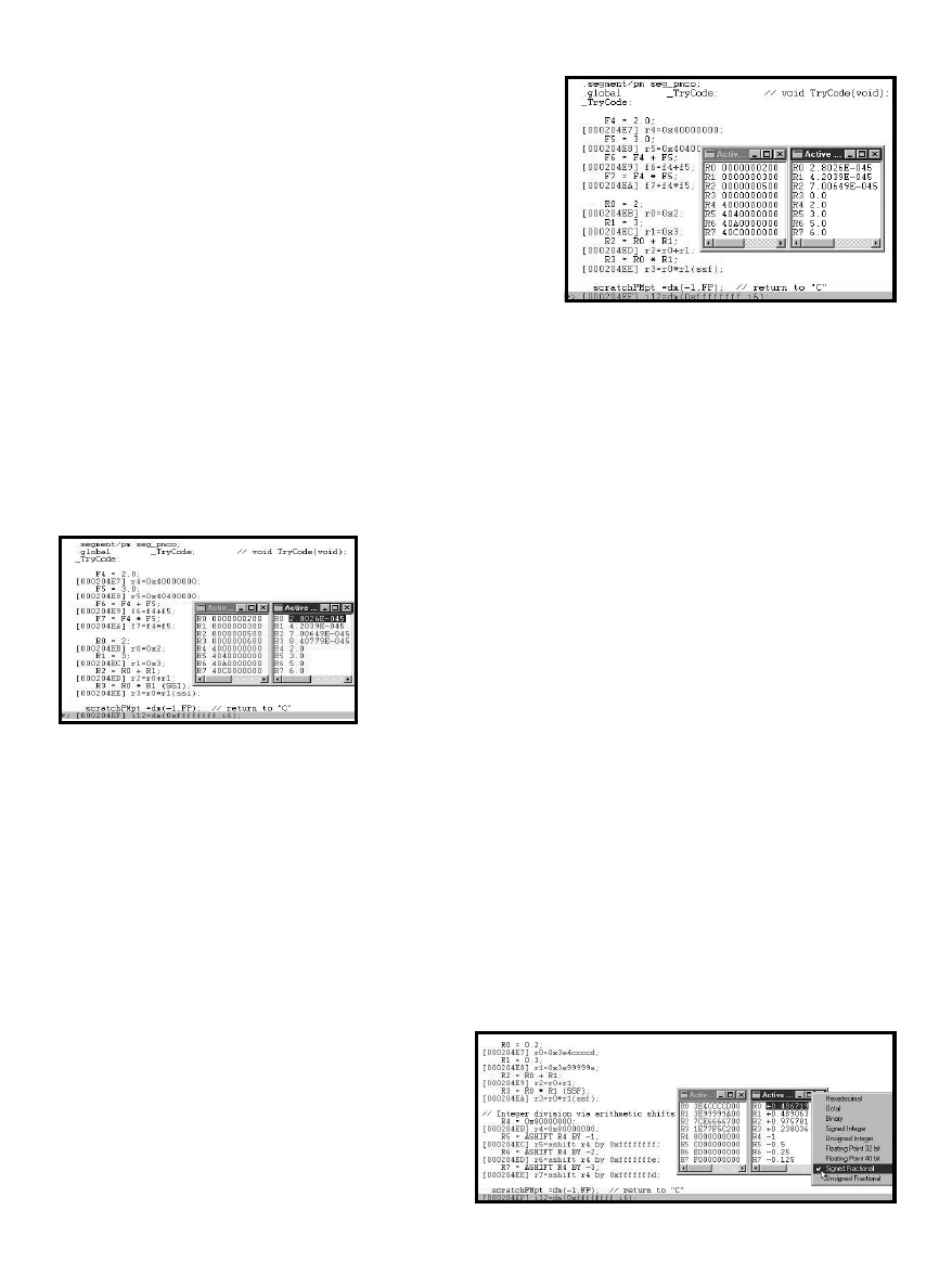
Photo 1 shows the White Mountain
VisualDSP SHARC simulator environ-
ment. The results are shown for several
basic assembly code operations. The
bit patterns in the data registers have
been interpreted using both integer
and floating-point formats.
Photo 1’s floating-point results
make sense (2 + 3 = 5 and 2 × 3 = 6).
But, the integer addition 2 + 3 = 5 has
been scaled by 0x100 to become:
0x200 + 0x300 = 0x500
Although unexpected, the addition
operation makes sense, unlike the 21k
integer multiplication operation,
which implies:
0x200 × 0x300 = 0
FEATURE
ARTICLE
Michael Smith
Just when you
thought it was safe to
continue on to the
later stages of DSP
application develop-
ment, Michael shows
us how quickly simple
problems can multiply
if left unresolved. The
right information can
be a lifesaver when
working with SHARCs.
Quirks and SHARCs
Photo 1—
Basic floating-point addition and multiplication operations on
the SHARC processor work as expected. However, even the simplest
integer addition and multiplication operations give incorrect results.
CIRCUIT CELLAR
®
Issue 127 February 2001
13
www.circuitcellar.com
As soon as you realize that there is one
thing about a processor that you don’t
understand, the floodgates open.
The AMD29k processor has a float-
ing-point instruction for division cal-
culations. It may be 11 times slower
than other 29k instructions, but it
exists, which is not true for the 21k
floating-point division instruction!
The 21k instruction set includes a
reciprocal instruction, but it doesn’t
appear to work as expected either.
The next issue involves fancy foot-
work with the internal operations of
the 21k processor to do something
neat—fast, single-cycle, floating-point
division. With any integer processor,
you can get fast division by powers of
two by using correct arithmetic shift
operations as shown by the following
68K instruction:
ASR #4, D0
gives D0 / 16
By understanding the bit representa-
tion of floating-point numbers, you can
perform comparable tricks to make
fast division (scaling) occur with float-
ing-point powers of two. This knowl-
edge could be particularly useful for
algorithms involving the FFT (fast
Fourier transform) algorithm. The
output from an inverse N-point FFT
requires scaling by a factor of N.
This fast division operation requires
checking and manipulating the float-
ing-point number’s binary component
bits. It’s more complicated to achieve
this on the 21k than on the AMD 29k
and Motorola 96000 processors (see
“Fast-Scaling Routine for Floating-
Point RISC and DSP Processors,” Cir-
cuit Cellar
52). The deep 21k instruc-
tion pipeline means there are several
cycle-stealing, delayed branch instruc-
tions associated with each
program decision (conditional
JUMP instruction). Some of
the problems can be overcome
by using the 21k super-scalar
and conditional compute in-
structions.
To get the most out of any
processor, you have to prop-
erly understand the conse-
quences of all aspects of that
processor’s architecture. De-
spite the apparently contradic-
tory characteristics of the 21k
architecture, they make sense.
There is a valid design decision
underlying every one of these
apparent ADSP SHARC processor
quirks.
MAKING 0X2 APPEAR AS 0X200
Because of the characteristics of the
68K processor architecture, a data
register showing bit pattern
0x800070FF can be interpreted in
different ways. For BYTE (8-bit)
operations, the register contains
the negative value 0xFF. The regis-
ter also can be considered as con-
taining the positive value 0x70FF
(16-bit word) or the negative value
0x800070FF (32-bit word).
In Photo 1, integer 0x2 appears
as the hexadecimal number 0x200
as a direct consequence of the in-
ternal architecture of the SHARC’s
data registers and ALU. Data regis-
ters are 40-bits wide to allow storage
of numbers in both the IEEE 754/854
standard 32-bit, single-precision, float-
ing-point format and an extended-
precision version of the same format.
Unlike the 68K processor, the sig-
nificant bits on the 21k data values are
at the high end of the register bit pat-
tern. This means that the last two
nibbles stored in a data register should
be ignored during interpretation or
when the value is written out to 32-bit
memory. The SHARC internal
memory architecture can be software
configured to handle both 32- and 40-
bit data memory operations.
GETTING 2 × 3 TO EQUAL 6
Because there are 32 significant bits
at the top of every 40-bit SHARC
register, it’s easy to understand why:
0x2 + 0x3 = 0x5
appears as operations using the values:
0x200 + 0x300 = 0x500
when the register contents are exam-
ined. But, it doesn’t explain why:
0x2 × 0x3 = 0x0
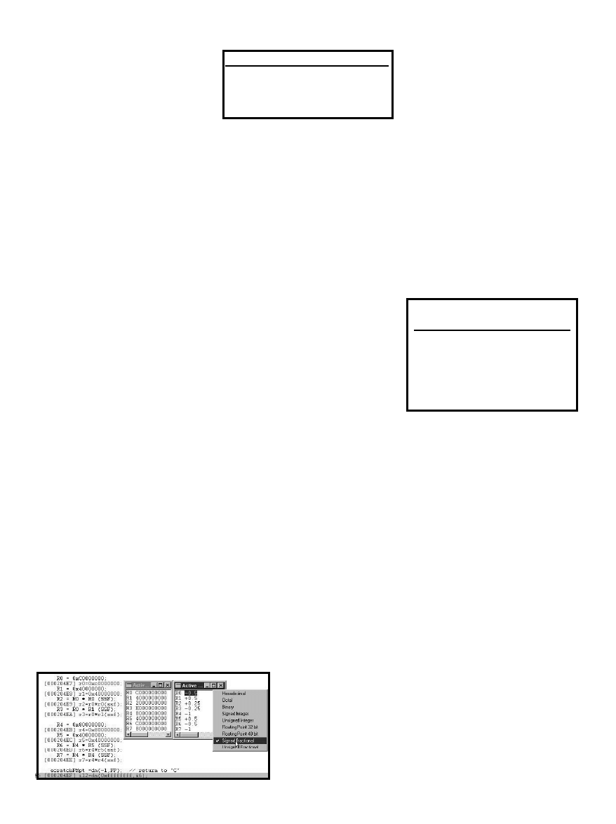
Photo 2 shows the program from
Photo 1. But, in this case, the display
mode for the VisualDSP development
environment is set to Mixed mode
rather than Source. During Mixed
mode, you see what you want to do
(source) and the bit patterns (assembly
code) associated with how the proces-
sor is interpreting those requests!
Photo 2—
The result of basic SHARC operations can be found in
the upper 32 bits of the 40-bit data register. Using the VisualDSP
development environment mixed mode display format, it can be
seen that the default SHARC integer multiplication instruction
expects a signed-signed fractional (SSF) number representation
rather than the standard two’s complement integer format.
Photo 3—
The SHARC processor starts acting like any
other processor after activating the signed-signed integer
multiplication operation rather than the default signed-
signed fractional format.
Photo 4—
Activating the
signed fractional inter-
pretation of the bit
patterns stored in the
integer data registers
shows that signed-
signed fractional opera-
tions are internally
consistent, even if they
don’t give the antici-
pated results.
14
Issue 127 February 2001
CIRCUIT CELLAR
®
www.circuitcellar.com
Let me explain why multiplication
operations appear to always give zero
or equivalent answers. Instead of per-
forming the intended standard multi-
plication operation R0 × R1, you
unintentionally activated R0 × R1
(SSF). SSF stands for the signed-signed
fractional form of the integer multipli-
cation instruction. [1]
The fact that an instruction comes
in both signed and unsigned forms is a
familiar concept. The 68K processor
has two types of multiplication opera-
tions, MULS (signed) and MULU (un-
signed). Many processors have three
forms of addition operations. The 29k
processor has ADDU and ADDS in-
structions, which cause exceptions to
the rules when the unsigned and signed
number representations overflow dur-
ing addition. And, ADD works when
you’re not worried about overflows.
The concept of a fractional repre-
sentation within an integer format
probably will send many overworked
developers back to old course notes.
But, it’s not what you need anyway, so
turn it off by using an explicit signed-
signed integer form of the 21k multi-
plication instruction, R0 × R1 (SSI).
Now the 21k processor is behaving
normally (see Photo 3). The 32-bit
operations 2 + 3 = 5 and 2 × 3 = 6 work,
even if the direct interpretation of the
32-bit values are distorted by storage
in the 40-bit SHARC data registers.
FLOAT OPERATIONS VIA INTE-
GER INSTRUCTIONS
In Photos 2 and 3, floating-point
operations of F4 = 2.0 are implemented
with the integer assignment that states
R4 = bit pattern for the constant.
Op-code bits aren’t used to describe
a floating-point assignment instruction
when the assembler can use an integer
assignment in conjunction with gener-
ating the bit pattern needed to repre-
sent a floating-point number.
This can cause a nasty consequence.
Suppose you write F4 = 2, where 2 is
an integer rather than a float (2.0). A C
language compiler would do the
equivalent of automatically casting
this expression as F4 = (float) 2 to give
F4
= 2.0. However, there is no equiva-
lent checking of context in the White
Mountain 21k assembler. The result is
R4 = bit pattern of integer 2. That
would give F4 a floating-point value
around 10
–45
, which wasn’t intended
(see Photos 1, 2, and 3).
This problem is more insidious
when initializing floating-point arrays
for filter coefficients with syntax:
.var array[3] = {1.0, 2.0, 3};
Two coefficients will be correctly
initialized, but the third coefficient
will be unintentionally too small. A
changed assembler operation would be
helpful so that warning messages are
issued. Perhaps a language extension
could be added to allow automatic
type casting, adding values 1.0, 2.0, and
3
to the array:
.var float array[3] = {1.0, 2.0, 3};
EXPERIMENTS WITH FRACTIONS
Don’t ignore this fractional integer
format. It must be useful within the
concept of DSP applications, otherwise
it wouldn’t be the default mode of 21k
multiplication operations.
The user manual for Analog De-
vices’ ’2106X indicates that the proces-
sor can support two 32-bit fixed point
formats. But, unless you have a text-
book to help you understand the mate-
rial, it’s best to experiment.
In Photo 4, an attempt has been
made to put fractional numbers into
integer registers and perform basic
addition and fractional multiplication
operations. The results in the data
registers are interpreted using the
signed fractional format available in
the VisualDSP development tool.
Now you’re heading in the right
direction. When compared to the ini-
tial signed fractional contents of the
registers, the final contents of the reg-
isters correctly indicate that:
0.4867 + 0.4890 = 0.9757
0.4867 × 0.4890 = 0.2380
The problem is that you were trying to
convince the processor to perform the
fractional operations:
0.2 + 0.3 = 0.5
0.2 × 0.3 = 0.06
FRACTIONAL INTEGERS
Setting the integer registers to frac-
tional values (R0 = 0.2 and R1 = 0.3)
doesn’t lead to the corresponding
signed fractional integer values (see
Photo 4). It’s strange that there isn’t a
built-in assembler directive to gener-
ate the bit patterns for fractional inte-
ger values. Miscalculating the
necessary hexadecimal bit patterns for
fractional values has been a constant
source of errors in my group.
But, a sensible relationship among
fractional integer values and their
hexadecimal representations has ap-
peared. Registers R5 to R7 contain the
results of applying a series of arith-
metic shifts (ASHIFT) to the greatest
negative 32-bit integer value
32-bit hex value
Fractional value
0x80000000
–1.0
0xC0000000
–0.5
0xE0000000
–0.25
0xF0000000
–0.125
Table 1—
Look at the relationship between the
internal hexadecimal representation and the 32-bit
integer value expressed as a signed fractional
value.
12-bit
Fraction of full-
hex value
scale A/D voltage
0x800
–1.0
0xC00
–0.5
0xE00
–0.25
0xF00
–0.125
0x000
0.0
0x100
0.125
…
…
Table 2—
The integer value from a 12-bit A/D
converter can be expressed as a signed value that
represents a fraction of the full-scale A/D converter.
Photo 5—
Most signed-signed
fractional multiplication operations
lead to the anticipated result.
However, the signed-signed frac-
tional multiplication of –1 and –1
would lead to the invalid result of
–1. The problem often can be
solved in an algorithm by using the
SHARC 80-bit accumulator associ-
ated with the integer multiplier.
16
Issue 127 February 2001
CIRCUIT CELLAR
®
www.circuitcellar.com
(0x80000000) in register R4. Using a
negative value with the 21k ASHIFT
operator produces an arithmetic right
shift, which is equivalent to signed
integer divisions by two (see Table 1).
A similar pattern of bits will be
familiar to developers who have spent
time hooking up a 12-bit A/D to the
data bus of a processor (see Table 2).
This equivalence suggests that one
way of looking at fractional signed
integers is to interpret the bit pattern
as a fraction of the magnitude that
can be represented in a signed, two’s
complement number representation.
Photo 5 shows that this is a con-
sistent interpretation with:
–0.5 × –0.5 (SSF) = 0.25
–0.5 × 0.5 (SSF) = –0.25
–1.0 × 0.5 (SSF) = –0.5
Photo 5 also hints that a deeper
understanding of fractional integer
representation is needed for proper
algorithm development because:
–1.0 × –1.0 (SSF) = –1.0
Fixing this problem in an algorithm
by using the 80-bit accumulator associ-
ated with the SHARC integer multi-
plier is the subject for another article.
21K FLOATING-POINT DIVISION
The AMD ’29050 processor has an
11-cycle, floating-point division in-
struction, FDIV. But, that instruction
complicates 29k assembly coding,
because it is slower than other 29k
floating-point operations and more
difficult to pipeline efficiently.
The majority of the 21k processor’s
instructions complete in a single cycle,
leaving no place for a slow, floating-
point division operation. The presence
of the 21k reciprocal instruction,
RECIPS, suggests a two-stage division
operation. First, the reciprocal of the
denominator is calculated in one cycle,
then the numerator is multiplied by
this reciprocal in a second cycle.
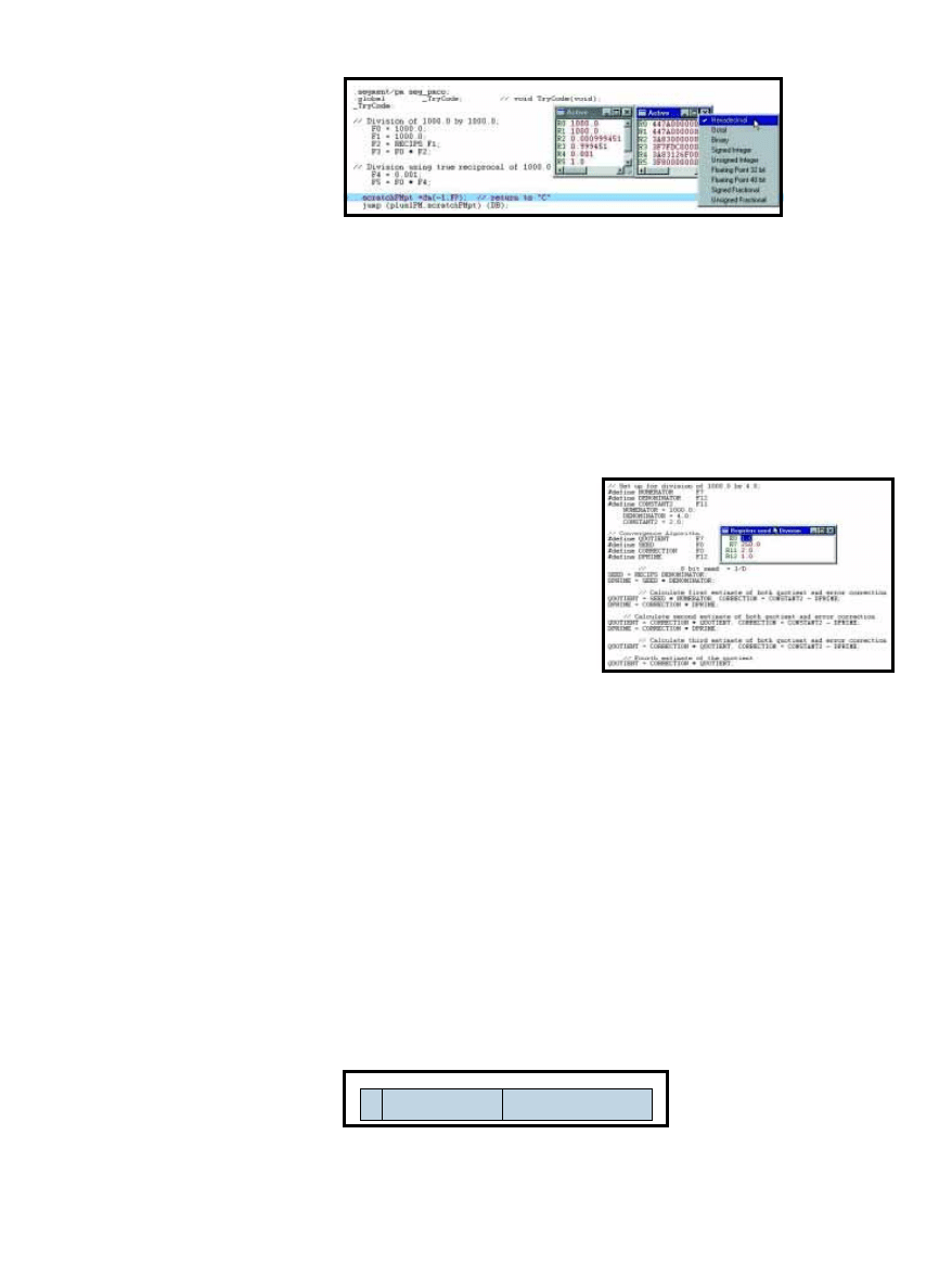
This approach doesn’t seem to work
using the RECIPS instruction (see
Photo 6). The approach, however, does
work if the reciprocal is directly evalu-
ated by hand.
This behavior is a result of the fact
that a ROM look-up table is needed for
reciprocals to be calculated in a single
cycle. High-accuracy reciprocals re-
quire an enormous amount of silicon.
Instead, a limited accuracy approxima-
tion (seed) of the reciprocal is calcu-
lated. For more information, read the
users manual. Comparing the hexadeci-
mal representations of the reciprocal
seed (F2) and the true reciprocal (F4)
reveals the limited accuracy of the
result from the RECIPS operation.
Photo 7 shows how a float-
ing-point division can be ob-
tained in eight cycles using the
super-scalar capability of the
SHARC processor and an itera-
tive convergence algorithm. [2]
A ±1-LSB accurate, single-preci-
sion quotient can be obtained
s
bexp—biased exponent
frac—fractonal field
31 30
23 22
0
Photo 6—
The
SHARC RECIPS
instruction provides
a limited accuracy
reciprocal seed
value in a single
cycle from a ROM
look-up table.
Photo 7—
A convergence algorithm is used to calculate
a floating-point division in eight cycles using the super-
scalar SHARC instructions.
Figure 1—
The representation of an IEEE standard floating-point
number takes 33 bits: one bit for the sign, 8 bits for the biased
exponent, and 23 bits for the fractional field. The thirty-third
normalization bit is hidden, not stored. s is the sign field, bexp
is the biased exponent field, and frac is the fractional field.
CIRCUIT CELLAR
®
Issue 127 February 2001
17
www.circuitcellar.com
after only six cycles. The choice
of data registers for the algorithm
is a consequence of the SHARC
architecture, which only allows
super-scalar operations among
certain banks of data registers.
CUSTOM DIVISION INTEGER
AND FLOATING POINT
As discussed, a fast, accurate
division instruction requires a
considerable amount of silicon.
Because most algorithms involve
only a few divisions, a compro-
mise is to have a slow instruction
(AMD 29k) or an iterative proce-
dure available (ADSP 21k).
One exception to this rule is
that division by powers of 2 (4, 8,
16…) happens frequently. Such
operations are needed to scale
integer inputs to ensure that the
algorithm does not overflow its
number representation, as
Laurence Turner and I discussed
in “Make Your Data Comfortable,
Get Bit Cushions,” (Circuit Cellar
125). Floating-point scaling by
Photo 8a—
Fast floating-point division by a factor of 2 can be imple-
mented via a single-cycle integer subtraction rather than an eight-
cycle iterative division. However, additional checks must be added
for accuracy.
b—
If the checks are incorrectly handled, the code
takes six or eight cycles as the SHARC’s instruction pipeline stalls.
a)
b)
powers of 2.0 is necessary for
outputs from algorithms such as
the inverse Fourier transform.
On the integer side, single-
cycle 21k arithmetic left and
right shifts can handle scaling by
powers of 2 (see Photo 4):
// Fast integer division R0 =
R1 / 16
R0 = ASHIFT R1 BY –4
However, floating-point numbers
are represented in a more com-
plex manner using three different
bit fields within a 32-bit register.
So, the shift approach for integers
must be changed to an equivalent
but different operation to achieve
floating-point scaling. This opera-
tion requires detailed under-
standing of the IEEE floating-
point number representation.
Figure 1 shows the 32-bit
representation of the three fields
of a floating-point number. Every
valid floating-point number can
be represented using format:
CIRCUIT CELLAR
®
Issue 127 February 2001
19
www.circuitcellar.com
SOURCE
ADSP21061 SHARC processor,
Analog Devices, Inc.
(800) 262-5643
(781) 329-4700
www.analog.com
REFERENCES
[1] Analog Devices, ADSP-2106x
SHARC User’s Manual
, 2d ed.,
1996.
[2] J. Cavanagh, Digital Computer
Arithmetic
, McGraw-Hill, New
York, NY, 1984.
Michael Smith is a professor at Uni-
versity of Calgary, Canada where he
teaches and researches introductory
and advanced microprocessor topics.
You can reach him at smithmr@
ucalgary.ca.
(–1)
s
× 1.frac × 2
(bexp – 127)
Figure 2 illustrates the transformation
of the decimal number 34.0 until it’s
stored as an floating-point value in
hexadecimal format.
Check out Table 3, which shows the
IEEE standard representation of pairs
of floating-point numbers. When bro-
ken into the three floating-point fields,
it’s easy to understand why pairs of
floating-point numbers that are scaled
by a factor of 16.0 differ by a fixed
value of four in their biased exponent.
With this information, a fast float-
ing-point scaling operation can be
handled through a single-cycle, sub-
traction integer operation that directly
adjusts the bexp bits of a floating-point
number (see Listing 1).
In principle, floating-point scaling
via integer operations can be imple-
mented on any processor, but does it
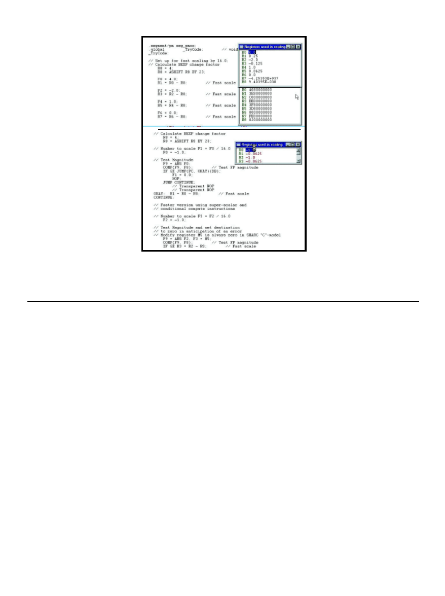
work? Photo 8a shows the code and
results for a series of floating-point
numbers divided by 16.0 in a single
cycle, rather than the eight cycles for a
standard SHARC division. The opera-
tion works well for scaling 4.0, –2.0,
and 1.0, but has a problem scaling 0.0.
The problem with 0.0 is that its
biased exponent is too small to allow a
valid floating-point number to be gen-
erated after four is subtracted to per-
form the fast scaling operation. This
problem didn’t occur with the integer
scaling operation using arithmetic
shifts. If the scaling factor was too
large, the significant bits were shifted
out of the value to leave zero. Some-
thing equivalent needs to happen for
the fast, floating-
point operations.
The scaling
approach works
when you can guar-
antee that every
number used has a
magnitude greater
than 2
(p –127)
, where
p
is the power of 2
by which you are
scaling. Photo 8b
shows two versions of a modified scal-
ing operation incorporated in the tests.
The first algorithm is slow (six cycles)
as the SHARC’s instruction pipeline is
exposed by the conditional jumps. The
second algorithm uses the SHARC’s
conditional compute and super-scalar
statements to avoid pipeline stalls
(three cycles).
You have now implemented an
accurate floating-point scaling opera-
tion that works faster at three cycles
than the standard eight-cycle SHARC
division. Was it worth the effort?
Nope! It’s just a neat party trick. If
you want to scale floating-point regis-
ters F0, F2, F4, and F6 by 16.0, the
simplest algorithm involving single-
cycle operations is:
F8 = 0.0625; // reciprocal of 16.0
F1 = F0 × F8;
F3 = F2 × F8;
F5 = F4 × F8;
F7 = F6 × F8;
WRAP UP
In this article, I discussed a number
of the characteristics of the Analog
Devices ’21061 SHARC processor.
These included internal representation
of integers, an unexpected default
setting for integer multiplication op-
erations, and a brief introduction to
fractional integers.
On the floating-point side, a tech-
nique was discussed for performing a
floating-point division in the absence
of a fast FDIV instruction. Details of a
faster, custom, floating-point scaling
operation were demonstrated using
conditional compute and super-scalar
instructions.
I
Author’s Note:
I thank Con Korikis of
Analog Devices University Support
and Tony Moosey of SHARC DSP
tools support.
Number
Internal hex
s
FP fields
FP representation
bexp
frac
1
0x3F80 0000
0
0x7F
0x00 00 00
16
0x4180 0000
0
0x83
0x00 00 00
–1
0xBF80 0000
1
0x7F
0x00 00 00
–16
0xCF80 0000
1
0x83
0x00 00 00
63.9625
0x427FD99A
0
0x84
0x7F D9 9A
1023.4
0x447FD99A
0
0x88
0x7F D9 9A
Table 3—
Floating-point numbers that differ by a scaling factor of 16.0 have
32-bit representations with biased exponent fields (bexp) that differ by 4. All
the other fields remain the same.
Conversion to binary value
34.0 = %100010
Conversion to 1.frac binary format
%100010 = %1.00010 × 25
Conversion to biased exponent format
%1.00010 × 25 = %1.00010 × 2(132 -127)
Identification of the 3 IEEE FP fields
s = %0 = 0x0
bexp = 132 = 0x84 = %1000 0100
frac = %000 1000 0000 0000 0000 0000
= 0x100000
Representation of 34.0 in 32-bits
= %0 1000 0100 000 1000 0000 0000 0000 0000
= %0100 0010 0000 1000 0000 0000 0000 0000
= 0x42080000
Figure 2—
The decimal number 34.0 goes through a
series of stages to identify the three floating-point
bit fields before being stored as the 32-bit value
0x42080000.
// Setup of BEXP adjustment factor
R0 = 4;
R0 = ASHIFT R0 BY 23
F4 = 1023.4;
// Integer operation to perform
// a single cycle FP division by 16.0
R4 = R4 – R0;
Listing 1—
Single-cycle FP division implements using integer operations.

20
Issue 127 February 2001
CIRCUIT CELLAR
®
www.circuitcellar.com
a
n altimeter is a
useful tool, espe-
cially for the outdoor
enthusiast. The
altimeter’s capabilities make it ideal
for trips, hiking, biking, and other
hobbies. In this article, I’m going to
describe an easy and inexpensive al-
timeter that includes a thermometer
and barometer.
This altimeter operates according
to the physical law that states atmo-
spheric pressure decreases with in-
creasing altitude. Both ambient
temperature and actual pressure can be
measured by the altimeter.
In addition, it has memory for 9 h of
data. So, when you return from a trip,
you can download the accumulated
data to a PC and read a profile of your
trip. The resolution
of the altimeter is
around 1 meter. It
recognizes if you lift
it from the floor to
your desktop! The
timing to make a
calculation is better
than with GPS tech-
niques, and it does
not need signals
from satellites.
One possible disadvantage is that
the altimeter can be affected by a baro-
metric pressure change. However,
experience shows it’s not a problem.
The altimeter is based on a P89C52
microcontroller, which collects and
calculates data from the temperature
and pressure sensors. Table 1 lists the
technical parameters.
CIRCUIT DESCRIPTION
The altimeter (see Figure 1) uses a
basic natural law that says atmo-
spheric pressure decreases with in-
creasing altitude. The basic formula is:
[1]
Three variables, T, p
0
, and p, have to be
measured. The first, T, is the ambient
temperature in Kelvins. p
0
is the atmo-
spheric pressure at zero level. And p is
the atmospheric pressure at the current
level. The remaining values are fixed
constants; R is the universal gas con-
stant (286 Joule/Kg/K) and g is the
gravitational acceleration (9.81 m/s
2
).
The altimeter measures T and p and
then recalculates actual pressure,
which is measured directly. Altitude
(based on Equation 1) is recalculated.
The ambient temperature could be
replaced by a standard value with
0.8
°
C decrease per 100 meters, but it’s
useful during a trip. Moreover, the A/D
converter has eight inputs available.
A similar principle can be used in
airplanes to measure speed using a
Pitot tube, but that was not the pur-
pose of this design.
The basic component in the altim-
eter is an MPX4115 absolute pressure
sensor. It provides calibrated output
voltage directly proportional to atmo-
spheric pressure. [1] Output voltage is
determined by:
FEATURE
ARTICLE
Radek Vaclavik
Whether you’re on
the road again or just
out to climb every
mountain, you’ll find
Radek’s digital altim-
eter project to be
quite practical. The
Design2K judges liked
it enough to award
him second place, so
take a look at what
went into the project.
An Altimeter for the
Traveling Man
Resolution of altimeter
1 meter
Usable altitude
0 to 2000 m
Barometer range
700 to 1100 hPa
Thermometer range
–30 to 30°C
Thermometer accuracy
1°C
Memory
10 h of data
Power supply
2.4 to 3.0 V, AAA batteries
Power consumption at 5 V
26 mA, 15 mA, 9 mA
DC/DC converter efficiency
70 to 80%
Table 1—
The basic parameters of the altimeter demonstrates a stable
resolution of 1 m.
CIRCUIT CELLAR
®
Issue 127 February 2001
21
www.circuitcellar.com
Value from altimeter
± difference
Absolute altitude
255
–1
368
1
1
369
0
0
369
0
0
369
2
2
371
253
–3
368
0
0
368
V
out
= V
s
(0.009 × P – 0.095) [2]
where V
s
is the supply voltage and P is
pressure in kilopascals (kPa).
The component’s sensitivity helps
determine the resultant resolution of
the altimeter. It is about 4.9 mV/hPa
for the MPX4115. Using Equation 1
and elementary mathematics, you can
determine that at a normal tempera-
ture, a 1-hPa drop is equal to about 8
meters. Conversely, a 1-meter change
in altitude causes about a 0.6-mV
change in output voltage.
All that remains is to determine the
necessary resolution of the A/D con-
verter. For a reference voltage of 5 V
and 1-meter resolution, you need:
[3]
This can be provided by a 13-bit con-
verter because 2
13
= 8192.
Many inexpensive 12-bit converters
are available. I used the AD7888 from
Analog Devices. If you use a 16-bit A/D
converter, theoretically you’ll get 14-
cm resolution. Remember that there
are more strict requirements for the
reference voltage stability, grounding,
blocking, and so on. Also, these convert-
ers are more expensive.
Another solution for better resolu-
tion is to amplify a signal from the
sensor using an op-amp. I use this
method in the altimeter.
The available power
supply limits this solu-
tion. With a 5-V power
supply and the required
altitude range, you can
use a maximum amplifi-
cation factor of 2.2.
Think about the
whole range of common
atmospheric pressure
(750 to 1100 hPa) and its
drop at an altitude of 2000 meters (see
Figure 2). The final range is from 600,
the lowest pressure at 2000 meters
with low atmospheric pressure, to
1100 hPa, the highest pressure at
0 meters with high atmospheric pres-
sure. When using Equation 2, you need
to process voltages from 2.3 to 4.6 V.
A complete diagram is shown in
Figure 3. The altimeter uses an
MC33502 op-amp IC6b. It is a
rail-to-rail type with a high-
input impedance. Its output
voltage can swing within 50 mV
of each power supply rail. Ampli-
fication is given by:
[4]
The input and output of IC6b
are measured relative to the
3.1625 VDC offset from the R3,
R2 divider at its non-inverting input.
The output is inverted, but isn’t a factor
because Equation 1 can be modified.
The resolution of the A/D converter
is increased by repeated measurement
and averaging of all values. The current
program version uses 256 cycles. Low-
pass filter R14 and C5 decreases the
noise of the sensor and maintains the
stability of the displayed value. [2]
The output is connected to the first
input of A/D converter IC2. The con-
verter uses a reference voltage equal to
4.6 V. The 4.6-V level
is a result of the altim-
eter’s power supply
level. Because you need
a few millivolts above
the reference voltage to
ensure good stabiliza-
tion, a 2.5-V program-
mable reference TL431
(D1) is used with am-
plifier IC6a.
The second input of the A/D con-
verter measures temperature. I used
the KTY81 (R13) sensor that forms a
divider with R12. R13’s resistance is
2000
Ω
at 25
°
C. The voltage reference
biases the divider. The output voltage
is proportional to ambient tempera-
ture. The basic resistance dependence
on temperature is approximated by a
second-order polynomial that’s calcu-
lated by microprocessor IC1. [3]
The third input is used for sensing
the 2.4-V power supply voltage. If the
battery voltage goes too low, then the
5-V power supply voltage will also
drop below 5 V. Values less than 5 V
will distort all measured data. If the
voltage is less than this limit, the al-
timeter will display a battery warning.
The A/D converter sends data
through a four-wire bus to the
microcontroller IC1 (P89C51), which
processes and calculates all formulae.
Equation 1 is easy to process on a cal-
culator, but not on a microcontroller;
programming is difficult if you use
only an assembler. Fortunately, com-
pilers can convert C language to binary
code, thereby making implementation
of a logarithmic function easier.
For the main program, I also used C
language in combination with assem-
bler routines for communication with
the display, memory, and A/D con-
verter. Figure 4 shows the flowchart.
All calculated data is displayed on
IC8, a 1 × 16 character display, which
is controlled via a 4-bit data bus and a
two-wire control bus. These wires are
shared with the A/D converter bus.
The display is the largest component
in the altimeter and could be replaced
by similar smaller types. The advan-
tage of using a common 1 × 16 display
is its availability and price.
Pressure
sensor
MPX4115
Amplifier
low-pass filter
DC/DC
Converter
MC33463
Battery
Display
1 × 16
RS-232
Interface
EEPROM
Microcontroller
P89C51UBPN
8-Channel
12-bit A/D
converter
AD7888
Reference and amplifier
Temperature
sensor
KTY81
5 V
2.4 V
4.6 V
0
500
1000
1500
2000
Sea level
1000
900
800
700
Pressure
Pressure (hP
a)
Altitude (m)
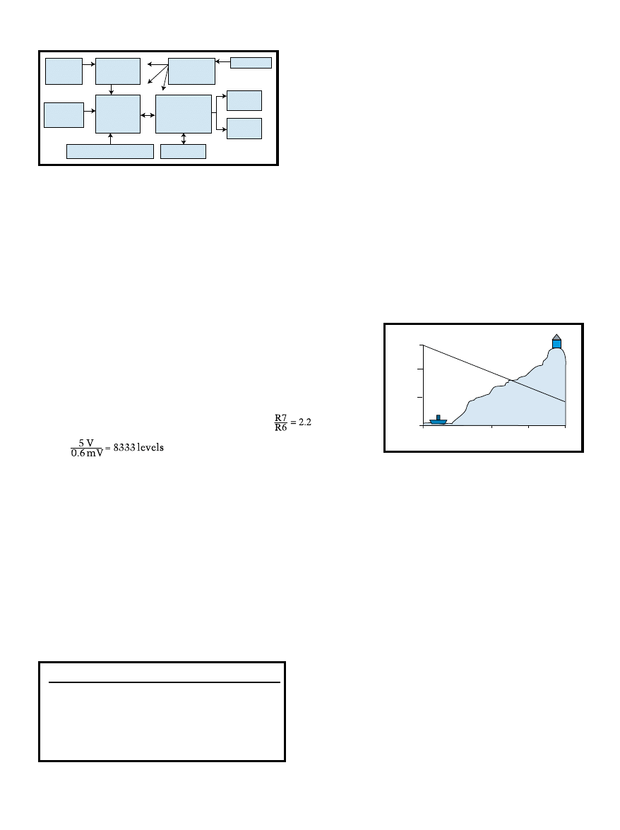
Figure 1—
The altimeter and Philips’s P89C51 microprocessor control
the display, memory, A/D converter, and RS-232.
Figure 2—
This illustrates the value of the pressure de-
crease with increased altitude based on Equation 1.
Table 2—
An example of data shows input value from the altimeter,
recalculated difference, and recalculated altitude.
22
Issue 127 February 2001
CIRCUIT CELLAR
®
www.circuitcellar.com
The altimeter provides the follow-
ing values: actual temperature, actual
atmospheric pressure, altitude, free
memory (as a percentage), and trip
duration in minutes. These outputs are
measured every 2 s and can be changed
periodically by pressing the Mode
button. Pressing the Set button while
any value is displayed sets a zero alti-
tude. Then, the altimeter switches to
show altitude (see Figure 5).
The altimeter also stores altitude
information and can download data to
your PC. Data is stored in EEPROM
memory IC9, which is controlled via
the I
2
C bus. Altitude data is stored
every 16 s; and with 2 KB of memory,
it can store 9 h of trip data. The sample
rate can be changed to a shorter period
of time, decreasing the capacity but
providing better resolution.
The Mem button is used to start
storing data in EEPROM memory. At
any time, you can interrupt or stop
storing data by pressing Mem again. If
data is being stored, an apostrophe is
shown in the display’s last position.
Also shown is the amount of free
memory. After exceeding maximum
memory capacity, the microprocessor
automatically stops storing data.
Data can be transferred simply to a
PC. T2 inverts the serial output from
the microprocessor. All common serial
ports are able to receive data with
levels of 5 or 0 V instead of ±12 V.
Importantly, this saves one integrated
circuit (i.e., MAX232).
Pressing the Mem button during
powerup initiates transfer of data to
the PC. After termination of the trans-
fer, the altimeter switches to its com-
mon function. Data format and data
processing will be described later.
There are two displayed values that
need calibration. First, you need to
calculate the correct value of R12 for
temperature. And, the atmospheric
pressure needs to be calibrated because
sensor IC7 varies from unit to unit.
The altimeter offers a special calibra-
tion menu that is started by pressing
Mode during powerup.
The calibration constants are in
integer format. You can increase or
decrease values by pressing the Mode
(+1) or Set (–1) buttons. When the cor-
rect value appears, pressing the Mem
button will switch to pressure calibra-
tion. Pushing it again will save data in
EEPROM memory and switch the
altimeter to common operation.
These constants are reloaded after
each start and are used for all calcula-
tions. The advantage of using EEPROM
is that you don’t need to modify the
master program or program the
EEPROM in a special programmer.
The best way to determine constant
values is to set them to zero, switch on
the altimeter, and write down the
difference between displayed values
and correct values. Then switch power
off and on and store these values in the
altimeter’s memory.
The altimeter can be powered by
2.4 to 3.0 V. IC3 is a DC/DC converter
MC33463 with a variable frequency.
[4] It uses accumulating coil TL1 and
filtering capacitor C6. This converter
doesn’t function with input voltages
greater than 5 V.
I use two rechargeable AAA, NiMH
batteries, but you can use AA depend-
ing on box size. Now, these batteries
have capacities as high as 550 mAh.
TL1’s resistance determines final
efficiency. A common SMCC choking
coil could be used. It gives about 75%
efficiency, but some special coils with
low resistance give about 80% effi-
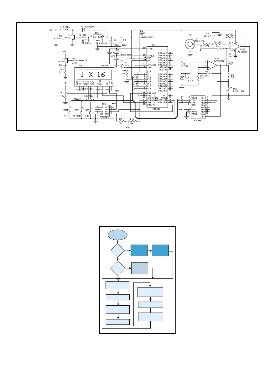
Figure 3—
This
detailed schematic
of the altimeter
clearly shows the
architecture from
Figure 1.
Start
Set?
Memory?
Input
calibration
data
Send
data to PC
Store
data to
EEPROM
Switch on
sensor BIAS
Measure data
Switch off
sensor BIAS
Calculate values
Display values and
store to memory
Idle mode
Wait 2 s
Figure 4—
The flowchart of the altimeter shows the
main tasks of the microcontroller. Tasks include
control of the power for the sensor and Idle mode.
24
Issue 127 February 2001
CIRCUIT CELLAR
®
www.circuitcellar.com
These short spikes are not visible in
Figure 6. Note that the current con-
sumption is about 9 mA. The cycle is
repeated every 2 s.
DATA PROCESSING
The altimeter sends data to the
serial port in standard format 8N1 (8
bits, no parity, 1 stop bit) at 9600 bps.
Any terminal program can receive
data; I use Hyperterminal from Win-
dows. The altimeter sends data sepa-
rated by a CR char (ASCII code 13). Set
the terminal to add an LF (ASCII code
10) so that data will be separated in
lines. Then, save the data.
The altimeter stores only the differ-
ence between the current value and the
last measurement because it saves
memory. Each value is 7-bits long and
the eighth bit is the sign. This means
that the altimeter can recognize a
change between the last two measure-
ments from –127 to 127 meters.
As I mentioned, I use Microsoft
Excel to process all of my data. Cur-
rently, I’m working on a macro that
will automatically process data and
create a chart. Soon it will be available
for free on my web site. For now, you
have to do it manually.
Now let’s look at an example of
data from my first trip. Two easy for-
mulae are implemented in the columns
of Table 2:
± Difference = IF(A1>127, (YES) A1-
256, (NO) A1)
where A1 is the cell with value from
the altimeter. The second formula is:
Absolute altitude = C0 + B1
where C0 is the previous altitude and
B1
is calculated difference.
You can use Table 2’s last column
to prepare a chart. Figure 7 is an ex-
ample of a profile of my first trip with
the altimeter.
BATTERY CHARGER
I also developed an easy-to-con-
struct fast charger for NiCd and NiMH
batteries used in the altimeter. I
looked for the simplest solution (see
Figure 8). The charger is based on an
MC33340, which was designed for
quick charges. This device uses nega-
tive slope detection for the end of
charging. Nickel cadmium and NiMH
batteries show a small drop in the
output voltage when they are 100%
charged. The MC33340 controls charg-
ing by detecting this decrease.
There is a backup solution to stop
charging in case the batteries are dam-
aged. The solution is an independent
timer that’s controlled by pins T1, T2,
and T3 and can be set up to 283 min.
Another possibility of how to stop fast
charging is detecting a high tempera-
ture of the battery.
The charger has two operating
modes. The first one is a Fast Charging
mode that is terminated by the meth-
ods just described. A blinking LED
diode signals this mode. The charger is
switched to the second mode, Main-
tain, when the batteries are powered
with a low current and the LED glows
steadily. This current covers self-dis-
charging of batteries so that they are
always ready for use.
The MC33340 can control the
LM317 voltage regulator, which is
useful because you don’t need a stabi-
lized power supply with an exact out-
put voltage. A power supply that
provides up to 18 V is enough.
You need to perform a few calcula-
tions to determine the values of the
resistors. These calculations are simple
and can be used for other applications,
as well.
Mode
Mode
Mode
Mode
Mode
Set
Mem
Temperature
Altitude
Altitude = 0
Start recording
Add to display
Free money
Pressure
Trip duration
Figure 5—
Three buttons,
Mem, Set, and Mode,
enable you to use all of
the altimeter’s functions.
The latest version of the
software offers more
capability.
Photo 1—
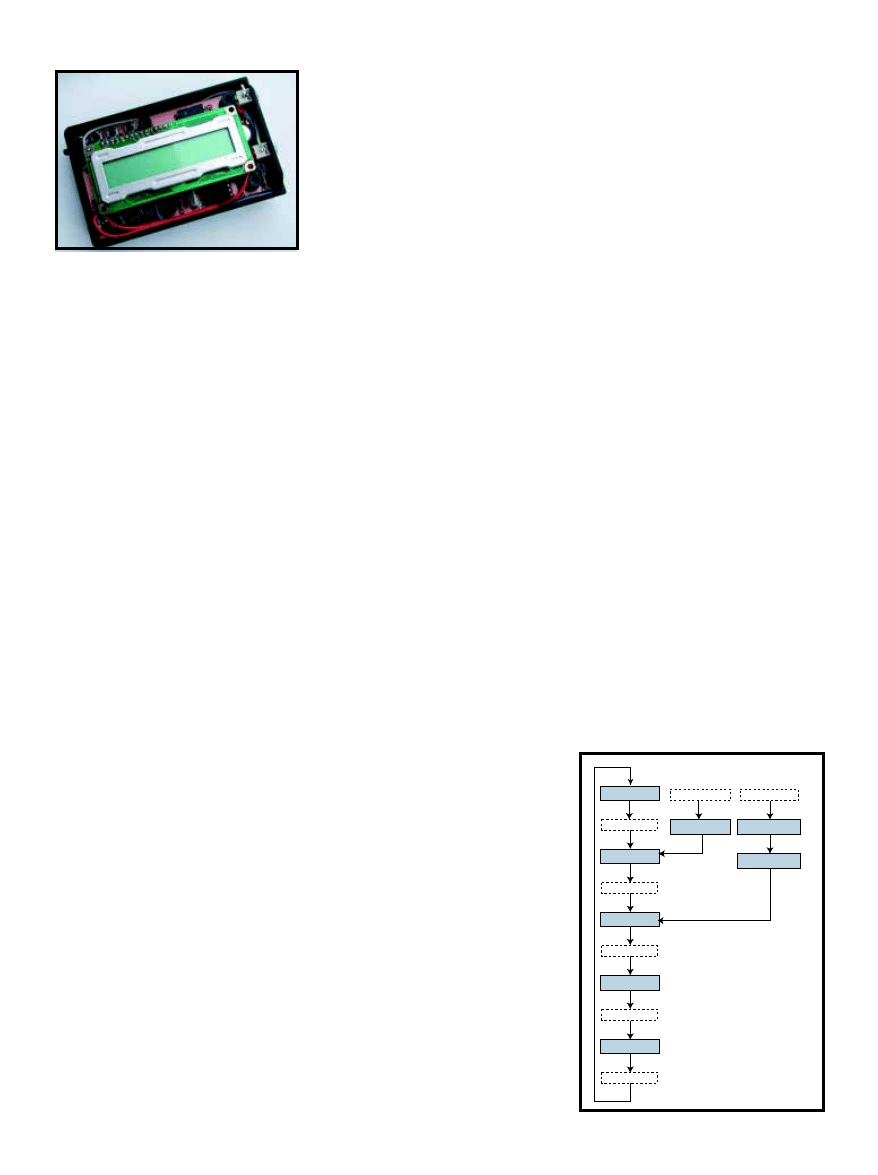
When looking at the display mounting,
the EEPROM is visible at the bottom. Also notice
that two white connectors are used for the RS-232
and charger.
ciency. Previous versions of the altim-
eter used a converter with an internal
switch and about 60% efficiency.
Of course, the altimeter’s power
consumption is important. I measured
these values without using power man-
agement. The A/D converter consumes
0.5 mA, the LCD consumes 1 mA, the
op-amp and sensor consume 8 mA, and
the microcontroller consumes 10 mA.
Notice that the sensor and op-amp
use a large portion of the energy, but
are not powered all the time. That’s
why I implemented PMOS switch T1
and simple power management. The
op-amp, pressure sensor, and reference
are powered only during measurement,
every 2 s. Delay loops are imple-
mented in the program to avoid bad
readings from the sensor. Also, the
microcontroller idles when possible.
T1 is a TMOS P channel transistor
from ON Semiconductor with low
resistance and can be controlled di-
rectly by the microcontroller. The
transistor is turned on with 5 V on its
gate and turned off with 0 V.
Figure 6 shows the current con-
sumption of the altimeter at 5 V. It
shows three phases of the work of the
altimeter. During phase 1, the altim-
eter also powers the pressure sensor
and collects data from the A/D con-
verter. The current consumption is
about 26 mA.
The sensor is not biased during
phase 2. At this point, the processor is
active and calculates all of the data. It
takes about 130 ms and 15 mA from
the 5-V power supply. During the final
stage of Idle mode (phase 3), the inter-
nal timer wakes it every 50 ms. During
this short time period, the processor
checks for pressed buttons.
26
Issue 127 February 2001
CIRCUIT CELLAR
®
www.circuitcellar.com
commence, thus protecting against bad
batteries. I selected R1 = 10 k
Ω
and R2
= 15 k
Ω
. These figures decrease the
battery’s 2.4 V to about 1.4 V, which
falls in the specified range.
Current drawn during the Maintain
mode should be about 0.03 to 0.05 of
battery capacity. I used cells with
500 mAh with 20-mA current. This
current is given by:
[6]
where V
in
is the input voltage and V
bat
is the voltage of the battery (2.4 V).
Then, with V
in
= 12 V and R5 = 455
Ω
,
you can use a 470-
Ω
resistor.
For the PCB, I decided to use a com-
mon DC connector with one switching
contact for the charger connection to
the altimeter. This contact unplugs the
altimeter’s electronics from the bat-
tery during charging.
ASSEMBLY AND DEBUGGING
The PCB is double-sided with a few
big holes for mounting it in a BOPLA
BOS-400 box. First, adjust the board’s
mechanical dimension with a file. The
box will need a few mechanical adjust-
ments, so use a knife to cut short pro-
trusions around the screws’ holes.
Then your PCB should match the box
exactly. The next step is to cut or mill
a window for the display, buttons, and
connectors. Dimensions for the win-
dow will depend on your materials.
After making the window, solder
the parts (except the microcontroller)
to the PCB. Connect the LCD via
Channel 1 500 mV
M 100 ms Channel 1
2.08 V
1–26 mA
2–15 mA
3–9 mA
Figure 6—
Simple power management was imple-
mented in the software. Period 1 represents pres-
sure measurement, period 2 shows calculations of
all variables, and period 3 marks the Idle mode.
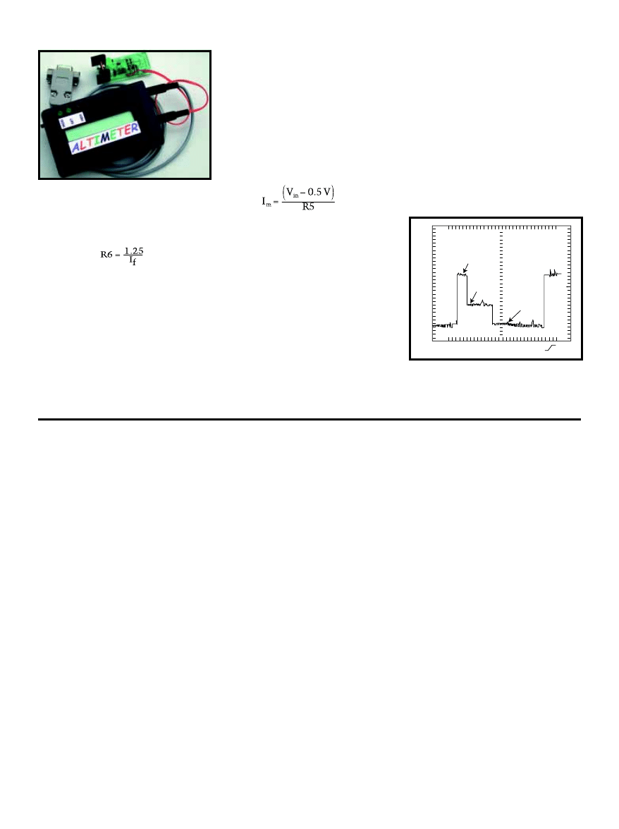
Photo 2—
Here’s the complete altimeter with
charger and cables.
Resistor R6 determines the fast
charging current and its value:
[5]
where I
f
is the charging current and 1.25
is the reference voltage of the LM317. It
should be chosen for a power dissipa-
tion of P = 1.25 × If. I selected 2 h of
charging with a current of If = 300 mA.
This gives R6 = 4
Ω
at 0.4 W.
R1 and R2 have to decrease the
battery’s voltage to 1 to 2 V. A voltage
outside of this range at pin 1 of
MC33340 won’t allow fast charging to
CIRCUIT CELLAR
®
Issue 127 February 2001
27
www.circuitcellar.com
SOURCES
AD7888
Analog Devices, Inc.
(800) 262-5643
(781) 329-4700
www.analog.com
Excel
Microsoft Corp.
(425) 882-8080
www.microsoft.com
Transistor, MC33340
ON Semiconductor
(602) 244-6600
www.onsemi.com
REFERENCES
[1] Motorola, Inc., MPX4115,
search.motorola.com/semiconduc-
tors/index.html.
[2] Motorola, Inc., “AN1646 Noise
Considerations for Integrated
Pressure Sensors.”
[3] Royal Philips Electronics,
KTY81-1,
www.semiconductors.com/pip/
KTY81.
[4] ON Semiconductor, MC33463,
SOFTWARE
The code and a parts list are avail-
golden pins and a precision socket (see
Photo 1) or with short cable. If you use
a socket for the microcontroller, you
may need to bend the display’s metal
holders.
There isn’t much space in the box,
so I use small audio jack 2.5-mm mono
connectors for charging and serial
output. This connector has contacts
that disconnect the altimeter from the
battery while it’s charging.
CHECKOUT
Connect the altimeter to a power
supply via an ammeter and check the
current consumption (see Photo 2). The
current shouldn’t exceed 50 mA at 2.4
V. Also, check the voltage at the out-
put of the DC/DC converter, which
should be 5 V. It’s important to take a
look at the 4.6-V reference at pin 1 of
IC6. Before taking measurements, tem-
porarily ground the T1 gate.
If everything is OK, solder the mi-
crocontroller or place it to the preci-
sion socket. After switching on the
power supply, the temperature will be
displayed and all functions of the al-
timeter should work. Next, perform
the necessary calibrations.
EVERYDAY USE
I developed this altimeter for a
hobby, not to compete with profes-
sionally made products. Professional
Figure 8—
The
MC33340 from
ON Semiconduc-
tor enables you to
charge the altim-
eter easily without
a stabilized power
supply.
Radek Vaclavik holds a college degree
in engineering. He is project leader at
ON Semiconductor Czech Design
Center. Radek is an active radio ama-
teur (call sign OK2XDX) and is inter-
ested in all aspects of electronics, from
DC to microwaves. You can find all of
Radek’s projects at his web site. He
may be reached at radek.vaclavik
@onsemi.com.
products are smaller but more expen-
sive. Moreover, I enjoyed constructing
the altimeter and seeing it work prop-
erly. The altimeter is easy to build and
debug and can be constructed by elec-
tronics beginners.
The parameters of the altimeter are
accurate, output values are stable, and
I achieved 1-meter resolution on all
units. Data storage is an interesting
option that enables you to see a profile
of the last trip. (There are visible
breaks where I stopped in some pubs.)
A GPS system will give you more accu-
rate values, but will cost more.
Other functions could be imple-
mented in the program. I’m working on
implementing an infrared port that
enables wireless transfer of data to a
PC. My next addition will process data
from a magnetic sensor on a bicycle
and enable gathering of profiles based
on traveled distance.
My latest altimeter version can
show altitude in feet, temperature in
Fahrenheit, and pressure in millimeters
of mercury. You can activate it by
grounding pin P3.6 of the microcon-
troller. Calibration must be done in
standard units, otherwise the software
will be difficult. An extended setup
menu lets you set your home altitude
and then the altimeter calculates the
absolute altitude.
You also can input an estimated
duration of the trip and the altimeter
will recalculate the internal constants
for better use of EEPROM memory. As
a result, you’ll get better resolution
because the altimeter will store the
altitude more often.
All new versions of SW require 8 KB
of program memory and use the 89C52
microcontroller instead of the 89C51.
The altimeter is a popular item at
my local cycle club because users can
compare achieved performance. After
0
1000
2000
3000
430
410
400
420
390
380
370
360
Time
Altitude
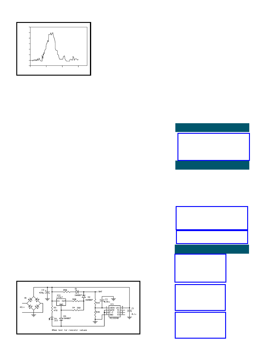
Figure 7—
When the prototype is ready, it’s time
to take a bicycle to the nearest hill and test it.
building this altimeter, I started an-
other project that I may write about in
the future. My newest creation is a
flying altimeter for use in model air-
planes. It transmits data down to the
modular. Keep an eye out for a story
about that project.
I

28
Issue 127 February 2001
CIRCUIT CELLAR
®
www.circuitcellar.com
a
fter the new
DVD player was
plugged into the big
screen TV and I saw the
image, there was no going back to
composite video. A few weeks later, I
purchased a programmable remote to
control my home theater system and
became a highly optimized couch po-
tato. But my happiness did not last.
A few months ago, I added a new
digital cable service. After installation,
I realized that the decoder box had an
S-video output. The problem was that
my TV had only one S-video input and
the DVD player was connected to it. I
found a manual S-video switch box at
Radio Shack. It saved having to switch
the cable behind the TV, but I was now
a sub-optimal couch potato.
Happiness (and optimization) could
only be found with a remote control-
led S-video switch. It was time to heat
up the soldering iron and write some
PIC code.
This project requires using a com-
mon IR format and detector so that an
off-the-shelf remote can act as the
controller. It needs to support four
input channels of S-video, composite
video, and stereo audio. There has to
be a learning mode so that codes other
than the programmed default can be
used to switch channels.
Also note that the mechanical form
factor should be no larger than the
Radio Shack mechanical switch. The
channels can be selected with front
panel switches and with a remote.
I researched the format of IR remote
controls and found that there are a few
major standards for IR protocols, in-
cluding the ubiquitous RC5 codes.
This format consists of 14 bits that are
transmitted using Manchester codes. I
settled on Sony’s remote control, also
known as the RECS 80 standard.
Sony’s protocol is simple and easy
to decode. And, Sony has a number of
excellent, after-market, universal re-
mote controls. Not to mention, I al-
ready owned one. In addition, it’s
logical to map the codes for the differ-
ent channels to the audio amplifier,
which I already owned as well.
Sony uses a 12-bit protocol that
consists of a 5-bit ID code followed by
a 7-bit command code. The data is
transmitted least significant bit first
after a start or AGC bit. On my oscillo-
scope, I observed that the start bit has
2.6-ms duration. A one was low for
1.44 ms, followed by a 440-µs termina-
tor. A zero was low for 760 µs, fol-
lowed by a 440-µs terminator.
The code to set a Sony amplifier to
the Video1 input is 822 hex (see Fig-
ure 1). Other observed codes for input
selection for a Sony amplifier are
stated in Table 1. For default codes, I
chose Video1, Video2, CD, and TV.
Note that you can teach the switch to
remember any combination of codes as
long as it adheres to the Sony format.
ENJOY THE CIRCUITS
The Panasonic PNA4613MOOYB
IR sensor, PIC16F84, and the Linear
Technology LT1204 4-input video
After upgrading his
home theater system,
only one thing hin-
dered Jerry from be-
coming the supreme
couch potato—the
manual S-video
switch for the TV. Not
to be deterred, he
built a remote switch
and continued his
quest for optimization.
Enabling the Couch Potato
Building a Remote-Controlled
AV Switch with S-Video
FEATURE
ARTICLE
Jerry Wasinger
Wasingerose
Figure 1—
Take a look at the Sony remote datastream observed at the output of the IR detector. This is the
code for 822 hex.
Start
0
0
0
0
0
0
0
0
0
1
1
1
CIRCUIT CELLAR
®
Issue 127 February 2001
29
www.circuitcellar.com
mux comprise this design. I used bicolor
LEDs to indicate the selected channel.
To modify this circuit to perform
tasks other than switching a video
mux, just tap off ADDR0 and ADDR1
with your own circuit. Or, use the LED
drivers as a set of one of four outputs.
The Panasonic IR sensor provides
the optical sensing, detection circuits,
40-kHz filtering, and amplification to
extract the signals from the remote.
The PIC has five pushbutton inputs,
one IR sensor input, four LED indicator
outputs, and two coded address selec-
tion outputs. Using an 8-MHz crystal
results in an instruction cycle of 500 ns,
or roughly two million instructions
per second, which is more than ad-
equate bandwidth for this application.
The LEDs have a circuit that allows
them to be controlled by one line. The
green LED is on and the transistor is off
when the input is high. The green LED
is off and the transistor turns on to
provide current for the red LED when
the input is low. The PIC outputs can
source up to 25 mA, which is more
than enough for an LED.
The LT1204 4-input video mux has a
30-MHz bandwidth that is adequate for
these signals. Here, you terminate the
inputs with 75
Ω
. So, you have to boost
the gain by two on the output. Other
devices, including Analog Devices’
AD8184 or the MAX454, can be substi-
tuted for this multiplexer. If the Analog
Devices part is used, a video amplifier
with a gain of two will have to follow
the outputs. For the audio switching, a
CD4052 dual 4:1 mux is used.
Power for the circuit is provided
with a 5-V linear regulator driven by a
common 9-VAC wall transformer. I use
a Linear Technology LTC660 inverter
to get the –5 VDC required by the
muxes. An LC circuit squelches re-
sidual switching noise from the in-
verter before going to the muxes.
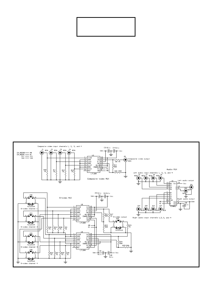
The three schematic diagrams illus-
trate the different sections of the cir-
cuit. Figure 2 shows the back end. The
front end consists of the muxes and
connectors (see Figure 3). And finally,
Figure 4 outlines the power supply.
SOFTWARE ANYONE?
The PIC program is straightforward.
After powerup, channel 1 is selected
by default. The code then goes into a
loop where it scans the buttons, main-
tains a timer, and waits for an inter-
rupt from the IR sensor. If a button is
pressed, it undergoes a debounce algo-
rithm before being processed. If an IR
signal comes in, each of the bits un-
dergo a timing analysis.
A bit is shifted into a buffer if it’s
valid. But, the process is aborted if a
bit is invalid. After 12 bits have been
shifted in, the code is compared to the
four values stored in EEPROM. If a
match is found, the PIC switches to the
appropriate channel. The program
button allows you to program any of
the four channels with code different
than the default. The new code is then
822h
Video1
81Eh
Video2
81Dh
AUX
821h
Tuner
825h
CD
Table 1—
The multiplexer uses four of the control
codes generated by the Sony remote. Here are nine
possibilities.
823h
Tape1
869h
Tape2
86Ah
TV
820h
Phono
Figure 2—
The circuit’s back
end shows all the muxes and
connectors used to route the
signals.
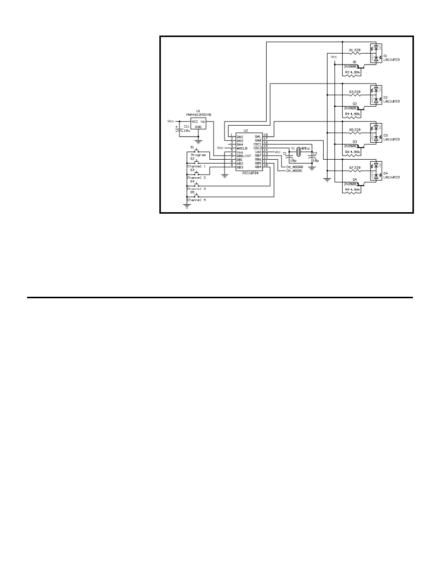
30
Issue 127 February 2001
CIRCUIT CELLAR
®
www.circuitcellar.com
stored in EEPROM and retained even if
power is removed from the circuit.
The code was written as a basic
multitasking system with interrupt-
driven events generating flags that are
detected and acted upon by an execu-
tive loop. The code in the interrupt
service routine (ISR) was kept short to
keep from blocking a concurrent event.
The core routines are the main loop,
interrupt service routine, button de-
coding, and IR data decoding. At
powerup, the PIC hardware is set up to
generate an interrupt on the falling
edge of the IR detector output. In addi-
tion, the timer is set up to generate an
interrupt every 128 µs. This period is
the basic tic used for debouncing the
switches, measuring the width of
pulses, and generating delays.
The main loop,
exec_loop, moni-
tors five of the bits in Port B to detect
if a button is depressed. If any of the
bits are low, the
button_scan routine
is called so that the depressed button is
isolated and debounced. This routine
returns a code that is then passed to
the
parse_buttons routine.
The switching of the signals going
to the LEDs and muxes is nested in
parse_buttons. The loop also moni-
tors the INCOMING_IR flag. This is
set by the ISR when the IR decoder
detects a falling edge. When a falling
edge occurrs, the
ir_decode subrou-
Figure 3—
The circuit’s front end
contains the IR detector, PIC chip,
buttons, and bicolor LEDs.
tine is called. If a valid IR code is re-
ceived, it’s encoded while
parse_
buttons is called again.
There is a special case during the
parse_buttons routine when the
program button is pushed. When this
occurs,
prog_butt is called, which
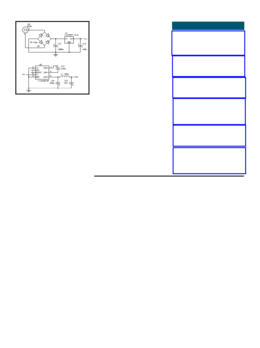
CIRCUIT CELLAR
®
Issue 127 February 2001
31
www.circuitcellar.com
SOURCES
Universal remote control, amplifier
Sony Electronics Inc.
(941) 768-7669
(800) 222-7669
www.sel.sony.com
PICSTART PLUS, PIC16F84
Microchip Technology Inc.
(480) 786-7200
www.microchip.com
PNA4613MOOYB IR sensor
Matsushita Electric Corp. of
America (Panasonic)
www.panasonic.com
LT1204 4-input video mux,
LTC660 inverter
Linear Technology Corp.
(408) 432-1900
www.linear-tech.com
AD8184
Analog Devices, Inc.
(617) 329-4700
www.analogdevices.com
MAX454
Maxim Integrated Products, Inc.
(408) 737-7600
(800) 998-8800
www.maxim-ic.com
Figure 4—
The power supply circuit uses a basic linear
regulator to generate 5 V and a Switch mode inverter to
generate the –5-V supplies.
Jerry Wasinger received his BSEE from
University of Oklahoma and his MSEE
from Colorado State University. Cur-
rently, he is director of engineering at
SpectRx, Inc. Jerry runs a web site for
electrical engineers called WebEE
(www.web-ee.com) and still enjoys
designing and assembling electronic
circuits. You may reach him at
webmaster@web-ee.com.
causes the LEDs to blink green and red
while waiting for you to push one of
the four channel select buttons.
After you select a channel, the next
routine to be called is
wait_4_ir. The
LED associated with the pushed button
is set to yellow by modulating it with
a 50% duty cycle while the processor
waits for an IR sequence from the
decoder. If a valid code is received,
parse_buttons calls save_code,
which stores the code in EEPROM.
The data in EEPROM is 10 bytes—a
high and low byte for each IR code and
two bytes of checksum data. If the
stored checksum does not equal the
value calculated from the four codes at
powerup, the software writes the de-
fault codes to the EEPROM.
The
ir_decode subroutine shifts
the 12-bit code from the remote into
the IR_H and IR_L registers. Monitor
the INCOMING _IR flag during this
process. The UP_COUNTER register
clears when the ISR sets the flag.
UP_COUNTER is incremented every
128 µs by the ISR.
The code then waits for the rising
edge of the IR signal. When this occurs,
the value in UP_COUNTER is com-
pared to the width of a zero and the
width of a one. A tolerance of two tics
is allowed for this measurement to
compensate for variations in remotes
as well as variations in the timing loop.
If the bit width is valid, its value is
shifted from the left into the IR_H and
IR_L registers. After 12 bits have been
shifted in, a 100-ms delay occurs to
allow any repeated or erroneous codes
to complete.
CONSTRUCTION TIPS
You’ll want to twist the signal and
matching ground leads from the S-
video connectors to decrease any pos-
sibility of radiation and make them
less susceptible to interference.
For packaging, I pulled out the me-
chanical switches from my switch and
placed my electronics inside. This gave
me a more aesthetic assembly with
being able to use all of the S-video and
RCA connectors on the back.
To program the PIC, you need a PIC
assembler and programmer. I used the
PICSTART PLUS development system
from Microchip Technology and it
works well.
I
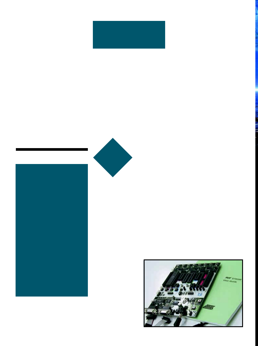
32
Issue 127 February 2001
CIRCUIT CELLAR
®
www.circuitcellar.com
t
his month, Cir-
cuit Cellar
and
Atmel are kicking off
the Design Logic 2001
contest. If you’re not familiar with
Atmel’s AVR family, follow along and
I’ll explain some of the details about
designing with the AVR microcontrol-
ler. The only thing left for you to do is
to request your sample part or order the
development kit (see Photo 1).
The AVR series is a RISC-based, 8-
bit microcontroller family with 20
devices that are available in package
sizes from 8 pins to 44 pins. The AVR
architecture is optimized for use with
high-level languages such as C.
The core processor in all AVR de-
vices is the same. All
devices have flash-based
program memory (except
the FPSLIC series) and
execute essentially the
same instruction set. The
AVR family is available
with an array of options;
some parts have a single 8-bit timer,
others have multiple 8- and 16-bit tim-
ers. Some parts have multiple channels
of 10-bit ADCs and some have one or
more UARTS for serial communica-
tion. Table 1 shows a breakdown of the
major features.
THE HARDWARE
The AVR parts share many common
hardware features. The program mem-
ory in most of the devices is stored in
flash memory. This permits you to
erase and reprogram the devices in-
circuit. Unlike EPROM, no UV light
source is required to erase the flash
memory . All AVR devices can be
erased or programmed using a serial
interface; the larger parts (20 pins or
more) also support a parallel program-
ming mode.
All AVR devices have some
EEPROM, ranging from 64 bytes to
4 KB. This memory can be written by
the software and retains its contents
even if power is removed. Writing to
the EEPROM isn’t like writing to the
internal RAM. The EEPROM requires a
specific sequence of events to prevent
spurious writes when the power is
changing or the state of the CPU is
otherwise unstable.
The EEPROM can be programmed
externally, using the same interface as
the flash memory. External program-
ming enables you to do things like add
compensation values for voltage refer-
ences when the circuit is tested on the
production line.
Another common feature of AVR
devices is 32 internal 8-bit registers. For
some of the smaller parts, this is the
only RAM the devices contain. Unlike
many microcontrollers with a dedi-
With great cash
prizes on the line in
the Design Logic
2001 contest, Stuart
offers his design ex-
pertise on Atmel’s
AVR microcontrollers.
There’s a whole prize
category devoted to
the AVR family, so
read up and then get
started on your entry!
Working with AVR
Microcontrollers
A Design Logic 2001 Primer
FEATURE
ARTICLE
Stuart Ball
Photo 1—
A development kit,
like this one for the STK500, is a
great place to start on your
contest entry.

34
Issue 127 February 2001
CIRCUIT CELLAR
®
www.circuitcellar.com
cated accumulator (or working) register,
the AVR architecture will let you
perform almost any operation on any
of the 32 registers.
That “almost” is an important con-
sideration. The register set is broadly
broken into two halves; the upper 16
registers support any register-based
operation. The lower 16 support only
some of these operations. Some of the
registers can be paired to do double
duty as 16-bit pointers. These paired
registers can be used as general-purpose
registers if the pointer function is not
needed (see Figure 1).
AVR registers are implemented as a
block of SRAM. Along with the 32
registers, most AVR devices have addi-
tional SRAM ranging from 128 bytes
to 4 KB located in a contiguous block
at the end of the register space.
The AVR processors execute one
instruction per clock cycle. Although
this may not seem like an important
architectural consideration, it is. Many
processors divide the external clock to
produce the necessary internal phases
for the CPU, resulting in an instruction
clock that is a submultiple of the input
clock. Microchip’s PIC processors, for
example, divide the external clock by
four, so a 20-MHz clock is required to
achieve a 5-MHz instruction rate. The
original 8031 divides its clock by 12.
The AVR processors execute one CPU
clock per input clock. A 10-MHz input
clock equals a 10-MHz instruction rate.
Like all microprocessors, some AVR
instructions take longer than one clock
cycle to execute. Immediate instruc-
tions take two cycles to execute, branch
instructions take one to three cycles,
and so on. But the one-clock-per-cycle
feature can reduce EMI in your system,
because you don’t need that 20-MHz
clock to get a 5-MHz instruction rate.
All microprocessors require a reset
after powerup to ensure that the hard-
ware is in the correct state. AVR pro-
cessors have a reset input, but they also
have internal reset logic that monitors
the power supply voltage and ensures
that the chip is correctly reset. External
reset components aren’t required.
When enabled, the AVR processor’s
watchdog timer generates a reset if the
CPU doesn’t refresh it before it times
out. The watchdog timer runs from a
separate 1-MHz internal oscillator. It
can be programmed to produce time-
outs from 16 ms to 2 s.
The simpler AVR devices have an 8-
bit timer. More sophisticated parts may
have an additional 8-bit timer as well as
16-bit timers. The 16-bit timers sup-
port input capture (capturing the value
of a free-running counter when an input
pulse occurs), output compare (generat-
ing an output or interrupt when a free-
running counter reaches a certain
value), and PWM output capability.
In some versions, internal UARTs
provide serial communication to the
outside world or to other processors.
Multi-channel ADCs are available
on some AVR devices. These use a
single ADC and an input multiplexer
to convert multiple input channels.
Some AVR devices provide an inter-
nal oscillator to eliminate the need for
an external crystal. This also frees two
pins for use as general-purpose I/O. The
internal oscillator is not as precise as a
crystal, so some of the parts provide a
means to adjust the clock when the
flash memory is programmed.
Most AVR general-purpose I/O pins
can sink up to 20 mA, so they can be
used to directly drive LEDs or other
devices that need high sink current.
The pins cannot be driven beyond the
positive supply (V
cc
), so they can’t be
used to drive high-voltage devices. If a
pin is used to directly drive a relay or
solenoid coil, be sure to add a zener or
clamp diode so the fly-back voltage
doesn’t destroy the AVR.
Using a direction register, you can
choose on a bit-by-bit basis whether a
pin is to be used as an input or output.
There is one direction register for each
I/O port and one bit in the register for
each I/O pin.
When you read a port, the AVR
architecture lets you read either the
state of the output register or the state
of the port pins. Execute an OUT in-
struction to write data to a port. Ex-
ecute an IN instruction to read data
from a port. IN Portx reads data from
the output register and IN Pinx reads
the external port pins.
Many AVR devices include an on-
chip analog comparator. This circuit
compares two analog voltages and sets
the output high if the positive input is
CIRCUIT CELLAR
®
Issue 127 February 2001
35
www.circuitcellar.com
higher than the negative input. The
output is low if the negative input is
higher than the positive.
The output of the analog comparator
can be directly read by the AVR soft-
ware or it can generate an interrupt.
The interrupt can be programmed to
occur when the comparator output goes
high, low, or changes state. On AVR
devices with timers that have input
capture capability, the comparator can
be programmed to trigger the input
capture function.
THE SOFTWARE
AVR processors execute an instruc-
tion set that consists of 118 basic in-
structions. The larger ATmega parts
have additional instructions to support
their extended memory addressing
range. Smaller devices with no internal
SRAM (other than the 32 registers) do
not support instructions that involve
accessing the additional memory.
AVR processors include special
function registers that control various
things such as the direction of the I/O
pins (input or output) and timers’ mode
of operation. The AVR instruction set
permits you to set and clear individual
bits in the I/O ports and in the special
function registers.
As mentioned earlier, six of the 32
registers can be paired as pointer regis-
ters for accessing either SRAM (in pro-
cessors that have SRAM) or program
memory. There are specific instructions
that access memory using these register
pairs and specific instructions that
permit simple 16-bit math for manipu-
lating each pair as a single entity.
Several instructions are dedicated
to moving data using the pointers.
These permit the pointer register pair
to be pre- or post-decremented (or
incremented) when a move is per-
formed. These special instructions
simplify the software and prevent
potential race conditions that could be
caused by an interrupt occurring be-
tween a move and increment/decre-
ment instruction pair.
AVR processors support several
interrupts. Which interrupts, of course,
depend on which peripherals are in-
cluded in your chip. Interrupt vectors
are located in the flash memory starting
at location 0000. The first vector is the
reset vector and the interrupt table
grows upward from there. Each vector
location is one-word wide, so the table
consists of a string of jumps to the vari-
ous interrupt service routines.
The AVR processors include a stack
to save return address for calls and
interrupt servicing. On smaller devices
without SRAM (such as the ’1200) the
stack is implemented in the hardware
and is of limited size. On devices with
internal SRAM, the stack is located in
SRAM and accessed via a stack pointer
register. On devices with less than
256 bytes of RAM, the stack pointer
register, SPL, is 8 bits. On devices with
more than 256 bytes of SRAM, the
stack pointer is a register pair (SPH and
SPL) to access the additional space.
The software must initialize SPH and
SPL (typically to the top of SRAM)
before enabling interrupts or executing
any subroutine calls.
On AVR devices that do not contain
internal SRAM, the stack is only three
levels deep and there is no stack
pointer to initialize. If you use nested
interrupts (an interrupt service routine
can be interrupted), be careful not to
overflow the stack. Also, the stack can
be used only to store return addresses;
the PUSH and POP instructions are not
operational on these parts.
TOOLS
Atmel provides a free AVR assem-
bler that can be downloaded. This
R31
R30
R29
R28
R27
R26
R25
R24
R23
R22
R21
R20
R19
R18
R17
R16
R15
R14
R13
R12
R11
R10
R9
R8
R7
R6
R5
R4
R3
R2
R1
R0
{
{
{
Z register
Y register
X register
Immediate instructions
(AND, OR, load, subtract)
and bit set/clear instructions
can be performed only
on these registers.
Figure 1—
Operations
such as add, subtract,
AND, OR, complement,
compare, increment,
decrement, XOR, and
load/store (direct and
indirect) are restricted to
the upper 16 registers.
The first six registers are
used in pairs as pointer
registers for indirect
addressing. Some 16-bit
arithmetic can be per-
formed on these six.

36
Issue 127 February 2001
CIRCUIT CELLAR
®
www.circuitcellar.com
package is a macro assembler that
produces object code (hex files)
ready to be programmed into an
AVR device’s flash and EEPROM.
Many of the low-level details
such as register management are
avoided if a high-level language is
used. C compilers for the AVR
processors are available from IAR,
ImageCraft, and SPJ Systems (see
Sources at the end of the article).
Atmel provides starter kits for
the ATtiny devices, the 20- and
40-pin parts, and a third kit for
the ATmega parts. Atmel also
provides emulators. The starter
kits include a basic AVR develop-
ment board and device program-
ming capability.
Third-party programmers for
AVR devices are available from
several companies (see Sources). A
’Net search for “AVR program-
mer” will reveal a number of web sites
describing parallel port-based program-
mers that take advantage of the serial
programming capability of the AVR.
DESIGN CONSIDERATIONS
Most of the AVR devices that have
an ADC use an external reference volt-
age. This voltage can be between 0 V
and the AVR supply voltage, V
cc
. Ana-
log input values can range between 0 V
and the reference voltage. The simplest
approach to generating a reference
value is to connect the reference to V
cc
.
This eliminates the need for an exter-
nal reference, but the precision of the
conversion is limited to the accuracy
of the V
cc
regulation.
The ATtiny15 has an internal
2.56-V reference for its ADC. Analog
inputs can range between 0 V and the
reference voltage. According to the
datasheet, the reference has a toler-
ance of about 6%, so this is the best
accuracy you can achieve with no
modifications.
You can apply your own reference
to the ATtiny15, but one way to get
better precision out of the internal
reference is to apply a known, precise
voltage to the chip when it’s pro-
grammed. If the software knows what
the ADC value should be with the
nominal 2.56-V reference, it can calcu-
late a correction factor for the actual
reference voltage using:
AVR
*Reset
Data out
Instruction in
Clock in
Clock in
Instruction in
Data out
Low-voltage programming
AVR
*Reset
Data out
Data in
Instruction in
Clock in
Clock in
Data, instruction in
Data out
High-voltage programming
+ 12 V
Resistor
2.2K
In-circuit programming when pins are also needed for I/O functions
During programming, apply serial programming signals to the AVR pin.
AVR
Figure 2—
There are two methods for serial programming.
(a)
shows
the low-voltage method while
(b)
shows the high-voltage method.
c—
During normal operation, if the AVR is an output, ground this point or
tie it high during programming to keep the programming wave form
from driving whatever logic connects here. If the AVR pin is an input,
you can leave it floating during programming.
a)
b)
c)
Device
Package pins,
Flash
RAM
EEPROM
Maximum
8-bit
16-bit
Other
I/O pins
(bytes)
(bytes)
(bytes)
frequency (MHz)
timers
timers
ATtiny10/11/12 8, 6
1024
0
64
8
1
0
ATtiny22
8, 6
1024
0
64
1.6
2
0
ATtiny15
8, 6
1024
0
64
1.6
2
0
Four 10-bit ADC channels
AT90S2323
8, 3
2048
128
128
10
1
0
AT90S2343
8, 5
2048
128
128
10
1
0
AT90S1200
20, 15
1024
0
64
12
1
0
AT90S2313
20, 15
2048
128
128
10
1
1
UART
AT90S2333
28, 20
2048
128
128
8
1
1
UART, six 10-bit ADC channels
AT90S4433
28, 20
4096
128
256
8
1
1
UART, six 10-bit ADC channels
AT90S4414
40, 32
4096
256
256
8
1
1
UART
AT90S8515
40, 32
8192
512
512
8
1
1
UART
AT90S4434
40, 32
4096
256
256
8
2
1
UART, eight 10-bit ADC channels
AT90S8535
40, 32
8192
512
512
8
2
1
UART, eight 10-bit ADC channels
ATmega161
40, 35
16,384
1024
512
8
2
1
Two UARTS, SPI
ATmega603
64, 32
64 K
4 K
2 K
6
2
1
UART, eight 10-bit ADC channels
ATmega103
64, 32
128 K
4 K
4 K
6
2
1
UART, eight 10-bit ADC channels
Table 1—
The comparison of parts in the AVR microprocessor family demonstrates a wide range of options that are suitable for almost any application.
Correction factor = Expected
ADC value/Measured ADC value
The correction factor is stored
in EEPROM and multiplied by all
subsequent ADC readings. Of
course, this requires that a pin be
available to put the device into
the special calibration mode. You
can do the same thing with an
external reference voltage. This
technique allows you to use a less
precise (and less expensive) refer-
ence for your application.
You can use a similar tech-
nique with other sensors. Ther-
mistors typically have a 5% or
10% resistance tolerance, which
translates directly into a tem-
perature measurement error. To
use this technique on a ther-
mistor, you have to hold the
thermistor at a precisely known
temperature for the calibration.
When you perform this type of
calibration, you can get correction
factors that are either greater or less
than one. To avoid doing floating-
point math in real time, you might
want to derive a multiply-and-shift-
right sequence to do the multiplication
with integer math. Another alternative
is to use a look-up table to correct the
ADC values.
The watchdog timer uses its inter-
nal 1-MHz oscillator. The exact fre-
quency of this oscillator varies with
supply voltage and temperature, and it
varies from one device to the next.
Consequently, you should allow for
variation in the value of the watchdog
CIRCUIT CELLAR
®
Issue 127 February 2001
37
www.circuitcellar.com
Sometimes you need more pins than
you have. A means to handle this is
shown in Figure 3. Here, one of the
pins is pulled high with a resistor. In
normal operation, this pin is used as an
output. To put the device into Calibra-
tion mode, the pin is grounded before
power is applied.
To use this scheme, the software
must check the state of the pin before
it programs the direction register to
make the pin an output. If the pin is
high, the code executes normally. If the
pin is low (having been externally
grounded to enable calibration) the
code enters the special Calibration
mode.
This example used an external pull-
up. You could accomplish the same
thing with the internal pull-up on the
port pin. However, these are large value
resistors, so the rise time will be slow
and the software may need to introduce
a delay before reading the pin.
Figure 3b shows how a single AVR
ADC input can be used to read two
switches. The analog input voltage has
four different values corresponding to
the four possible states of the switches.
The switches could be configuration
switches or user pushbuttons.
The AVR timers fall broadly into
two categories of 8- and 16-bit. All
AVR devices have at least one 8-bit
timer and some have two. The 16-bit
timers have more functionality than 8-
bit timers do. The timers can be
clocked from the CPU clock using a
programmable pre-scale value or from
an external pin.
timeout. For instance, if you program
the watchdog timer for a 2-ms timeout
and reset it using a 2-ms interrupt, you
may sometimes get a watchdog
timeout even though the reset is work-
ing properly. Or worse, the condition
may only occur at high temperatures
and not on all units.
Figure 2 shows how programming
the flash memory and EEPROM works.
All AVR devices without an internal
oscillator require that an external
crystal or clock source be connected
for programming. Devices with an
internal oscillator, such as the
ATtiny15, use that clock to time the
program operations.
There are two methods for serial
programming; low-voltage program-
ming is enabled by grounding the RE-
SET input and high-voltage
programming is enabled by applying
12 V to the RESET input. Not all of
the AVR devices support the high-
voltage mode. The timing diagrams in
Figure 2 are typical.
A problem you may run into with
in-circuit programming is the dual
nature of the pins. Ideally, you would
leave the ISP pins free for program-
ming, but this is not always possible.
This can make in-circuit programming
difficult.
One way around this problem is
shown in Figure 2c. A 2.2-k
Ω
resistor is
placed in series with the AVR pin. In
normal operation, the AVR pin can
drive external logic or it can function
as an input from external logic. During
programming, the control signals are
directly connected to the AVR pin.
This scheme requires that the pro-
gramming driver be able to drive both
high- and low-logic levels into the 2.2-
k
Ω
load, so a driver with suitable cur-
rent capacity is needed. Obviously, if
the AVR pin is being used as an output
that has to sink or source significant
current, this approach won’t work
because the series resistor will limit
the current available to whatever the
AVR is driving.
An alternative way to handle this
problem is to add logic external to the
AVR device that multiplexes the pins
between the normal function and the
ISP function. Of course, this compli-
cates the design of your circuit.
The simpler AVR timers are a
counter that can be clocked by a (pro-
grammable) pre-scale value from the
system clock or be clocked by an
external clock. These counters can be
loaded by software and generate an
interrupt when they roll over from FF
to 00. These timers have no provision
for a repeatable clock other than di-
vide by 256. If you want a divisor
other than 256, you have to reload the
timer each time the overflow inter-
rupt occurs. If you are using a /1 or /8
clock pre-scale, this can make the
time period vary by whatever your
interrupt latency variation is, because
the interrupt latency can delay inter-
rupt servicing until one or more timer
clocks have occurred.
Some AVR devices have more so-
phisticated 8-bit timers, which essen-
tially add an 8-bit compare register.
When the count reaches the compare
value, the compare register can generate
an output or interrupt the CPU. This
allows you to have a regular, repeating
interrupt generated in hardware.
Other AVR devices include 16-bit
timers. These include a compare func-
tion like the more complex 8-bit
counters. The 16-bit timers also have an
input capture function that captures the
AVR
V
CC
Resistor
2.2K
Output to
something
AVR
V
CC
R1
2.2K
Connect this pin to ground at
powerup to place AVR into
Calibration mode.
With V
CC
= 5 V:
S1 open, S2 open, V1 = 5 V
S1 closed, S2 open, V1 = 3.9 V
S1 open, S2 closed, V1 = 3.4 V
S1 closed, S2 closed, V1 = 2.9 V
(voltages are approximate)
R3
8.2K
R4
4.7K
S2
S1
V1
Figure 3—
Some-
times you need
more pins than the
device has, so
dual-purpose
inputs are handy.
(a)
shows using a
pin as a calibration
input and
(b)
shows using an
ADC input to read
two switches.
Timer value
Temporary register
Input capture register
Non-interrupt code
writes high byte
Non-interrupt code
writes low byte
Interrupt code
reads low byte
Interrupt code
reads high byte
?
? 53
53D7
22
2245
Interrupt occurs here
Timer value
Temporary register
Input capture register
Non-interrupt code
writes high byte
Non-interrupt code
writes low byte
Interrupt code
reads low byte
Interrupt code
reads high byte
?
?
53
22D7
22
2245
Interrupt occurs here
Figure 4—
Let’s say the non-interrupt code wants
to write a value of 53D7 hex to the timer registers
and the input capture register contains a value of
2245 hex.
(a)
shows how it’s supposed to work and
(b)
shows what happens when it doesn’t work.
b)
a)
b)
a)
38
Issue 127 February 2001
CIRCUIT CELLAR
®
www.circuitcellar.com
SOURCES
AVR devices
Atmel Corp.
(408) 436-4270
Fax: (408) 436-4314
www.atmel.com
AVR programmers
BP Microsystems, Inc.
(800) 225-2102
(713) 688-4600
www.bpmicro.com
Electrical Engineering Tools, Inc.
(408) 734-8184
Fax: (408) 734-8185
www.eetools.com
Needham’s Electronics Inc.
(916) 924-8037
Fax: (916) 924-8065
www.needhans.com
C Compilers
IAR Systems Software Inc.
(508) 485-2692
Fax: (508) 485-9126
www.iar.com
ImageCraft Creations Inc.
(650) 493-9326
Fax: (650) 493-9329
www.imagecraft.com
SPJ Systems
+ 91 20 5899048
www.spjsystems.com
AVR
Output
Q2
Q1
V
CC
V
CC
R1
Pull-up
R2
Pull-up
Figure 5—
Take a look at the AVR driving an H-
bridge. Make sure the power-up state of the pins
doesn’t turn on both transistors.
value of the free-running counter when
an input pin changes state. When using
input capture, the 16-bit timer can roll
over from FFFF to 0000. The software
must take this into account.
The 16-bit timers can switch an
output pin when the output compare
occurs. And, they can generate a PWM
output. Of course, any timer function
that uses an external pin makes that pin
unavailable for general-purpose I/O.
External clocking allows you to
operate the timer from a timebase
other than the CPU clock. The exter-
nal clock is internally synchronized to
the CPU clock, so the external clock
cannot be any faster than the CPU
clock. Some versions of the AVR allow
you to run a timer from a 32.768-kHz
crystal that is connected to two pins.
This allows you to use the timer as a
real-time clock.
Because the AVR is an 8-bit proces-
sor, the 16-bit timers must be loaded
in two operations. This is accom-
plished with a temporary register. The
software writes the most significant
byte of the register values, then the
hardware stores this value in the tem-
porary register. The software then
writes the least significant byte and
the hardware writes both bytes simul-
taneously to the timer registers.
Be careful if interrupts are used. The
16-bit timers have three registers, the
output compare, input capture, and
counter registers. There is only one
temporary register. So, if you use inter-
rupts and if the interrupts access the
16-bit registers, there is a potential for
a race condition when an interrupt
occurs (see Figure 4).
The timer register gets loaded with
the wrong value because the interrupt
occurred between the two timer writes
by the non-interrupt code. The result is
that the interrupt code modified the
temporary register before the non-
interrupt code could update the timer
registers. The way to avoid this is to
disable interrupts before the non-inter-
rupt code modifies the timer registers.
As with any design, make sure the
power-up state of the port pins does
not damage your hardware. For in-
stance, if you have two port pins driv-
ing both transistors in an H-bridge, be
sure that the power-up state doesn’t
turn on both transistors (see Figure 5).
In Figure 5, two port pins of the AVR
drive two MOSFET transistors in one
half of an H-bridge. At powerup, both
outputs are pulled high by the pull-up
resistors because the ports come up as
inputs (high impedance). Consequently,
both transistors turn on, making a short
between V
cc
and ground and probably
destroying one of the transistors. The
fix is easy, use an inverter to make one
of the transistors turn on when the
output is low. But it illustrates the
potential problem. Similar cases would
include two relays or two motors that
must not be turned on at the same time.
As mentioned earlier, the AVR pro-
cessors all have 32 internal registers.
Even when using a device with addi-
tional SRAM, many applications can be
implemented by using just the 32 regis-
ters. If you’re working in an HLL, the
compiler typically assigns the registers
for you. If you’re working in assembly,
there are a few things you can do to
make efficient use of the registers.
For example, when defining the
registers you’ll use, identify variables
that won’t be used with immediate
instructions and assign those functions
to the first 16 registers. Examples in-
clude counters that will be zeroed,
incremented, and decremented, but
never loaded with an immediate value.
Similarly, assign the registers that
need to be used in immediate instruc-
tions to one of the upper 16 registers. If
you have a general accumulator regis-
ter for some operations, make it one of
the upper 16 registers.
If you need several on/off flag values,
don’t use a complete register for each
flag. Instead, assign one of the upper 16
registers as a flag register, assign each
bit to be a flag value, and use the bit
set/clear/test instructions to manipu-
late individual bits. This can reduce the
number of registers you need.
For fast context switching, dedicate
registers for use in the ISR. By dedicat-
ing these registers, you avoid the time
needed to push and pop registers from
the stack. Of course, this won’t work if
the ISR needs a lot of dedicated vari-
ables or if you have a lot of interrupts,
because you will run out of registers.
THE BOTTOM LINE
AVR processors make a powerful
family of parts that are suitable for
many design tasks. With such a variety
of devices and options, you should be
able to find one for your application!
I
Stuart Ball, P.E., is an electrical engi-
neer with 20 years of experience. He
has written numerous articles and
three books about microprocessor-
based designs, all published by
Butterworth-Heinemann
(www.bhusa.com).

42
Issue 127 February 2001
CIRCUIT CELLAR
®
www.circuitcellar.com
EPC
R
EAL
-T
IME
PCs
Ingo Cyliax
A Cup of Java
Keeping it simple
has kept a couple of
spacecraft in orbit
for 30 years, but as
Ingo investigates the
issues of using Java
in embedded appli-
cations, he wonders
if the benefits of us-
ing Java might be
worth the added
complexity.
Part 3: Embedded and Real-Time
Solutions
i
recently read
something that
intrigued and inspired
me. NASA is going to
try to make contact with Pioneer 6, a
spacecraft that was launched in 1965,
to see if it still has a live connection.
Pioneer 6 is the oldest spacecraft that
is still functioning, and although most
of the scientific instruments on Pioneer
6 have since died, the probe was still
functioning in a stable orbit the last
time it was contacted in 1997.
The second oldest spacecraft is
Pioneer 10, which was launched in
1972 and is now seven billion miles
away, making it the next most distant
man-made object. Because of its range
we’ll probably lose contact with Pio-
neer 10 before it stops working. I don't
know about you, but I find it hard to
fathom that, in a time when Windows
crashes several times a day, something
can function in space for over 30 years
without a single service call.
For the last couple of months, I have
been exploring Java. In particular, I’ve
been looking at issues with respect to
using Java in embedded and real-time
applications. This month, I want to
look at what it takes to get into Java.
There are two components you need
to program and run Java applications.
First, you need a development environ-
ment and some kind of run-time envi-
ronment. Fortunately, coming up with
the development environment is fairly
easy. The de facto place to get your
Java development kit (JDK) is through
Sun Microsystems. The JDK (as well as
other Java components) can be down-
loaded for free from Sun’s web site.
There are two types of developers
kits available, the source development
kit (SDK) and the Java development kit
(JDK). In most cases, all you need is the
JDK. The JDK and SDK are available
for Win32, Linux, and Solaris, as well
as other Unix workstation environ-
ments. You simply download it for the
platform you’d like to develop on.
Because I’m a Unix and Linux guy, I
usually do most of my Java developing
under Linux or Solaris. Solaris is Sun's
operating system for its SPARC line of
workstations and servers.
After you download and install the
development kit for your platform,
you’re in business. You should be able
to write and run a small Java program.
The JDK and SDK include the Java run-
time environment (JRE) for your plat-
form because the Java compiler and
several of the Java development tools
are actually written in Java and need
the JRE to run successfully.
TINI (DEMITASSE CUP OF JAVA)
Now, you’re ready to look at some
embedded Java. I chose Dallas Semi-
conductor’s TINI Java platform to
illustrate some of the techniques and
issues involved in running embedded
Java applications.
TINI Java is a small Dallas 80390-
based microcontroller module. It’s a
complete system, including 512 KB of
flash memory, 512 or 1024 KB of bat-
Photo 1—
This is the TINI interface running on the
development host (Windows, Linux/Unix) and is
used to convert and download Java applications into
the Java module.
CIRCUIT CELLAR
®
Issue 127 February 2001
43
www.circuitcellar.com
tery-backed SRAM, an Ethernet con-
troller, and real-time clock all on a 72-
pin SIMM module. The module also has
two serial ports and a CAN controller
and runs from a 5-V power supply.
The firmware includes a loader that
allows you to download programs to
the flash memory on the module. You
can download your Java application
and even assembly language native
subroutines and they will run as soon
as you reset it the next time. There is
even a simple command line-based
interpreter and mini operating system
called the serial line user shell (slush).
With it, you can download programs
over the ’Net and modify files in the
on-module file system, as well as in-
stall passwords for users who want to
login via the network.
One nice feature is that this module
runs instantly. When the power is ap-
plied, the module is available. You can
drop your TINI module into an applica-
tion and it works when you turn it on.
The tool needed to download and
configure applications in the TINI Java
module requires an external API called
the communication API (CommAPI).
This API is a set of classes that can be
used to access serial and parallel ports
under Java in most run-time environ-
ments. CommAPI is needed on the
development host, so that the Java-
based download program can access
the local serial port to talk with the
module. This module is some-
what system-dependent and
there are different versions
available for Win32 and Solaris
(SPARC and i86). Notably miss-
ing is the Linux version of
CommAPI. At least Sun recog-
nizes this and points you to
some Linux resources. I decided
to go with the RxTx package.
RxTx is a GNU-based native
library that implements the
back end of the CommAPI inter-
face. This is installed as a shared
library that the Sun version of
JRE can use to access serial and
parallel ports under Linux. The
installation is not trivial, it
requires you to configure the
package and compile the librar-
ies before installing. It also
needs the Sun Solaris ’x86 ver-
sion of the CommAPI library for the
Java-based classes used to interface
with Java programs. The instructions
are good, and it was fairly easy to get it
running with the Java JRE included in
the JDK I downloaded. When CommAPI
and the native libraries are configured,
compiled, and installed, the TINI pro-
gram starts right up and is ready to use
(see Photo 1).
The TINI module from Dallas is
based on a JVM running on an 8-bit
microcontroller. Although there are
many JVM solutions available for 8-
and 32-bit processors, there are also a
few pure hardware solutions available.
These are known as direct byte code
execution processors and they imple-
ment the JVM instructions either di-
rectly in hardware or via microcode
extensions on the chip or hardware.
NEW GAME PLAN
I wanted to show you some example
applications running on the TINI Java
module, but unfortunately I broke it
and a replacement hasn’t arrived in
time to get this article out the door, so
I'll have to come back to it at a later
time. Instead, I want to look at a
sample weather station application
that comes in the development kit to
illustrate how Dallas APIs are used to
interface it to external devices and also
discuss some other Java hardware plat-
forms that are available.
Many of the native Dallas toolkits
have been written in assembly lan-
guage. This means that if one of the
methods in a class gets a call, it gets
vectored into an assembly language
subroutine to do its work. The devel-
opment kit, which is downloadable for
free from the Dallas web site allows
you to develop your own native func-
tions by providing an assembler and
linker for the ’390 microcontroller and
instructions. They do, however, warn
you about the potential to shoot your-
self in the foot. As the app note for the
native methods says, “We’ve given you
the gun and the bullets. Be careful
where you point it...and enjoy!” This
illustrates just how easy it is to become
complacent about worrying about
pointers and such in Java.
Dallas has collected some classes for
the TINI system. In particular, there
are classes to deal with interrupts,
serial posts, LCDs, CAN bus, and one-
wire and iButton-based peripherals like
thermometers. Photo 2 shows a shot of
the top-level class documentation
browser for the TINI classes.
One of the simple example applica-
tions that can be found in the TINI
development system is the LCD test
application. Listing 1 shows the com-
plete program. Note that this applica-
tion includes the
com.dalsemi.comm
class library. In general, the recom-
mended way to name your own class
libraries is to use your domain
name in reverse order. For ex-
ample, dalsemi.com would use
the
/com/dalsemi directory,
Sun Microsystems would use
/com/sun, or if I decided to
develop a class library, it would
be
/com/ezcomm. There are two
basic advantages to this. The
name is unique because only
unique domain names may be
registered, and if needed, you
could find the company on the
Internet.
One of the libraries that
Dallas provides is the comm, or
communication, library. This
library contains all of the gen-
eral communication interfaces
you may want to use. In this
case, you are interested in the
LCD library.
Photo 2—
Here’s the view from the TINI Class browser. This part of
the documentation lets you look at all of the available APIs.

44
Issue 127 February 2001
CIRCUIT CELLAR
®
www.circuitcellar.com
The program initializes the display
using the
LCDPort.sendcontrol()
method, which writes data into the
control port of the display. After ini-
tialization, the program uses
LCDPort.setAddress() to set the
character insertion point. It then needs
to convert the Java testing string to an
ASCII byte stream.
This may sound strange to you, but
remember that Java has a special type
it uses for the string data. It’s a 16-bit
quantity per character and uses
Unicode for encoding the string data.
Unicode is not compatible with the
LCD display, so you have to convert it
to standard ASCII bytes using the
String class getBytes() method.
When converted to bytes, you can use
the
LCDPort.sendBytes() method to
write the display data to the display.
This program illustrates one way to
use the native methods that have al-
ready been developed by Dallas and
added to the class library. Other classes
include
com.dalsemi.comm.CanBus,
which handles the CAN bus controller
and
com.ibutton.*, which takes care
of iButton peripherals.
import com.dalsemi.comm.*;
public class LCDTest
{
// on my LCD, 4 lines. The address of the beginning
// of each line(decimal) is 0, 40, 20, 84
public static void main(String[] args)
{
int addr;
System.out.println("Starting LCDTest");
if (args.length < 1)
addr = 0x00;
else
addr = (new Integer(args[0])).intValue();
System.out.println("Using address " + addr);
LCDPort.sendControl(0x38); //Set up the display mode
LCDPort.sendControl(0x0C); //Turn on display with no
cursor
LCDPort.sendControl(1); //Clear
LCDPort.setAddress(addr); //Set address of first
character
String s = "Testing"; //String to display
byte[] d = s.getBytes();
for (int i = 0; i < d.length; i++)
{
LCDPort.sendData(d[i]);
}
}
}
TINI represents an inexpensive way
to explore embedded Java. The TINI
module can be purchased on iButton's
on-line web store, and the development
software is free, even if Sun’s Java stuff
takes some effort to set up under Linux.
OTHER AVENUES
There are some other embedded Java
solutions. LavaCORE from Derivation
Systems is a direct execution processor
core that has been implemented on
FPGAs. The core can be parameterized
to exclude instructions that are not
used by a fixed application program to
reduce the size of the hardware. The
idea is to analyze the application and
generate customized core and system
components like timers and I/O to build
a system on a chip optimized to run a
specific application. Of course, you can
also build a general-purpose core.
aJile Systems has two Java chips, the
aJ-80 and the aJ-100. The aJ-100 is a
newer version of the aJ-80 chip and
includes extensions to run real-time
applications. Both chips are direct
execution JVMs, which means the code
doesn’t need to be translated to run.
Listing 1—
This simple program is used to test the LCD interface and API for the TINI Java system.
It prints “Testing” to the LCD display.

CIRCUIT CELLAR
®
Issue 127 February 2001
45
www.circuitcellar.com
aJile also offers a couple of evalua-
tion modules based on its chips. The
first one is the aJ-PC104, which is
based on the aJ-80 processor and in-
cludes Ethernet, serial ports, general-
purpose I/O, and a PC/104 stack
interface. aJile will soon offer a new
SBC based on the aJ-100.
Patriot Scientific took a slightly
different approach to executing Java.
The psc-1000A is a 100-MHz stack-
based machine with byte code-based
instructions similar to the JVM. This
makes it possible to translate Java
class codes one-to-one to run on the
Patriot CPU, maintaining similar code
density to Java byte code and faster
interpreted speeds.
The nice features of this chip in-
clude a virtual peripheral unit (VPU),
an I/O controller on the chip that can
be programmed independently to per-
form I/O operations. There are also
various general-purpose I/O pins and
memory controllers for DRAM,
SRAM, EPROM, and VRAM.
Patriot also has C compilers that
allow you to run compiled C programs
mixed with translated Java programs.
Also, Wind River’s VxWorks has been
ported to this chip, and evaluation
boards are available from Patriot.
One of the application areas for
embedded Java is industrial control,
where you need reliable processors and
systems. The increased safety that the
language and executing environment
can offer over traditional C/C++ imple-
mentations makes Java a good fit.
Also, consider that in applications
like industrial control, the systems
tend to have long lifetimes (sometimes
as long as 10 years). You want to be
able to make enhancements and up-
grade late in the life cycle of the prod-
uct if necessary. Because Java is an open
architecture, it will always be possible
to reverse engineer a Java-based system
and execute the software.
In contrast to closed systems, you
may have to make a snapshot of the
development environment, including
the hardware, if you plan to make en-
hancements down the road. As an ex-
ample, consider my plight a couple of
months ago when I tried to hunt down
a V. 5.0 Microsoft C compiler in order
to recompile a piece of software I
Ingo Cyliax is a computer and electri-
cal engineer (BSCEE) and the founder
of EZComm Consulting, which special-
izes in embedded systems and FPGA
design services as well as troubleshoot-
ing. Ingo has been writing about vari-
ous topics ranging from real-time
operating systems to nuts-and-bolts
hardware issues for several years. He
can be reached at cyliax@
ezcomm.com.
SOURCES
JDK, SDK, JRE
Sun Microsystems, Inc.
(650) 960-1300
www.sun.com
TINI Java, iButton
Dallas Semiconductor Corp.
(972) 371-4448
Fax: (972) 371-3715
www.dalsemi.com
LavaCORE
Derivation Systems, Inc.
(760) 431-1400
Fax: (760) 431-1484
www.derivation.com
aJ-80, aJ-100, aJ-PC104
aJile Systems Inc.
(408) 557-0829
Fax: (408) 557-8279
www.ajile.com
psc-1000A
Patriot Scientific
(858) 674-5000
Fax: (858) 674-5005
www.ptsc.com
needed to fix. To take this to an ex-
treme, I have old DOS CAD software
that will not run on a modern version
of Windows because it needs to have
access to dongles and has graphics
libraries for specific chipsets that are
not available for bus structures found
in more modern PCs.
Other industries are evaluating Java
architectures for control systems where
long system lifetimes, high reliability,
and perhaps remote upgrades are impor-
tant. Maybe future space probes will be
programmed in Java to run some variant
of Java hardware. On the other hand,
Pioneer 6 and Pioneer 10 owe their long
life in part to the KISS (keep it simple,
stupid) design philosophy.
I
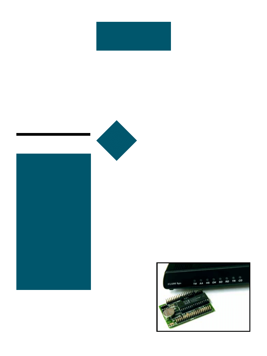
46
Issue 127 February 2001
CIRCUIT CELLAR
®
www.circuitcellar.com
EPC
Applied PCs
Fred Eady
One Thin DIME
Once again Fred
sets out to show us
that the rumors
about the death of
DOS may have
been greatly exag-
gerated. Although a
dime won’t get you
very far today, you
can travel the world
wide web with just a
DIME and a Stamp.
hen was the
last time you used
DOS to format a
diskette or hard disk?
When was the last time you issued a
DOS command in a wholly DOS envi-
ronment? Were you born with a
mouse in your hand and think DOS is
a window in WIN98?
Well, I can honestly tell you that I
formatted a hard disk drive with DOS
not long ago. I also issued some pretty
neat DOS commands in the process,
and I was around before the mouse was
invented. In fact, as a consultant and
writer I deal with DOS on a daily basis.
Why am I rambling about DOS? Every-
body knows DOS is dead. As musical
maiden Madonna would say, “Not!”
DOS still lives in multiple flavors
under the cover of embedded comput-
ers. As far as I’m concerned,
if DOS can get you on the
’Net, it ain’t dead. When
DOS was born, a dime could
buy a cup of coffee. Nowa-
days, a DIME is a DOS token
you can use to hitch a ride on
the Internet.
CAN YOU SPARE A DIME?
The “D” in DIME stands
for DOS Stamp. As you might
have guessed, the DOS Stamp
is a DOS-based miniature
single-board computer de-
w
signed specifically for embedded con-
trol applications. Although tiny in
size (2.6" × 2.0" × 0.625"), the DOS
Stamp is made up of I/O, storage,
processing, communications sub-
systems, and a real DOS operating
system. The DOS Stamp’s application
software may be written with familiar
DOS-based software tools like Borland
C and C++, Microsoft C and Visual
C++, compiled QuickBASIC, and
PowerBASIC to name a few. (Not only
do I use DOS every day, the Florida-
room library sports all of the afore-
mentioned programming tools, too!)
A standard DOS Stamp is powered
by an AM188ES CPU clocked at 40
MHz. Memory is organized as 512 KB
of SRAM with 256 KB of flash
memory organized as 128 KB of flash
memory disk with 128 KB reserved for
BIOS and DOS. A Disk-on-Chip is
available and the DOS Stamp has 8
MB of it as well as the optional 8-
channel, 12-bit ADC in the guise of a
MAX197. Dallas’s DS1689 keeps time
for the DOS Stamp.
Remember how (relatively) easy it
was to put a DOS executable to-
gether? You wrote the source code
using a QB or Borland C editor. Then
a compile process was invoked and
the bits came out the end of the tube
with an .
exe extension. Everything
you needed that wasn’t related to the
compiler was supplied by your
machine’s BIOS and the services of
DOS. Your new executable, or .
exe
file, was loaded into memory with the
assistance of DOS. When loaded, the
application could call on BIOS ser-
vices to provide the low-level inter-
face to the actual hardware. It’s still
Photo 1—
It’s even tinier than the diskettes that spawned its OS.
Getting on the ‘Net with DOS
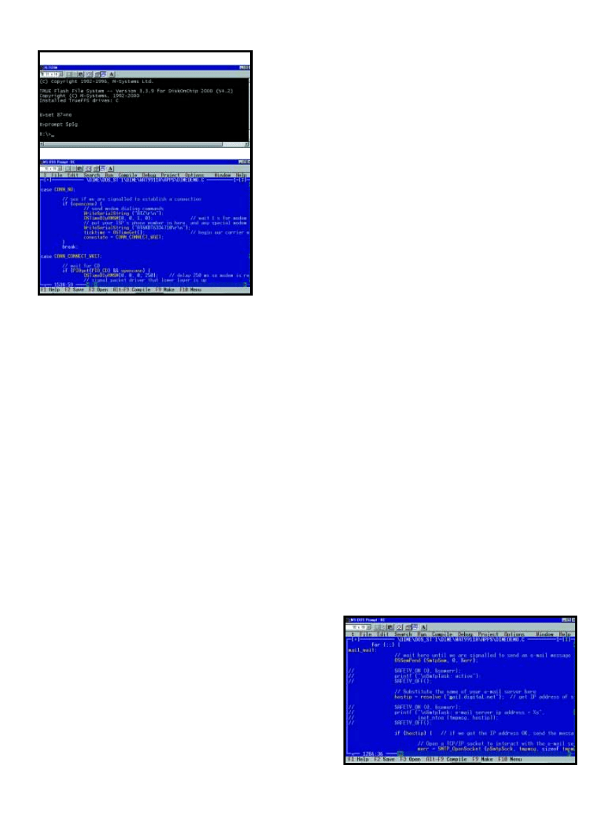
CIRCUIT CELLAR
®
Issue 127 February 2001
47
www.circuitcellar.com
that easy with the DOS Stamp, which
uses the BIOS and DOS resources just
like your ’386 did in the days of old.
As you can see in Photo 1, the DOS
Stamp is much smaller and prettier
than your ’386.
The “I” is for Internet. This makes
the DOS Stamp special. The DOS
Stamp is surrounded by a software
suite that allows the DOS operating
system to be used with an embedded
platform to access the Internet.
Like all good Internet players, the
DOS Stamp follows the standards that
comprise the Internet. To put the DOS
Stamp on the Internet, you need extra
DOS Stamp hardware and a C com-
piler. The DOS Stamp comes standard
with a second serial port to be used
for connecting the modem that came
with my version of the DIME. To
keep the source code as DOS Stamp-
compliant as possible and to avoid
having to scratch my head in confu-
sion, I’ll use the recommended Borland
C++ V.3.1. The bits will flow on the
DOS Stamp COM2 serial port. DTR
and DSR are not used and RTS is tied
to CTS. The RX and TX lines are used
as is and the RS-232-level DCD line is
regulated using a series resistor and
internal clamp diodes of the DOS
Stamp’s I/O pin.
In addition to the DOS Stamp hard-
ware and options and the Borland
compiler, I’ll need a couple of ISP
accounts with mail and
Internet Explorer to show
how the DIME does the
Internet. No problem be-
cause the Florida room is
equipped with Road Runner
and a standard dial-up ISP
account. For those of you
who don’t have access to
Road Runner yet, this is a
cable modem hookup.
On the Internet software
side, the DOS Stamp em-
ploys eTCP/WATTCP for
TCP/IP services. The DOS
Stamp is capable of TCP/IP
and UDP communications
and uses PPP and PAP for
dial-up connection to the
Internet. PPP is simple to
understand but difficult to
deploy, and is used to estab-
lish connection to the Internet. The
DOS Stamp does all of the magic I
discussed last time around.
PHASE IN, PHASE OUT
The PPP link starts out as dead. The
physical layer, which includes the
CPU’s UART, modem, modem cable,
and phone line, is then awakened and
the Establish mode is entered. After
the UART and modem establish com-
munications among themselves, the
ISP or remote peer is dialed. Upon
answering, the DOS Stamp and re-
mote computer become peers. Why
peers? Well, that means that neither
the DOS Stamp nor the remote com-
puter is in total control of the session.
At this point, LCP (link configura-
tion protocol) takes over and at-
tempts to negotiate the link
characteristics. These characteristics
may include the packet
size limits or the au-
thentication protocol.
The magic number may
also be used by LCP to
determine if the link is
in loop-back mode. If
terms can’t be agreed on,
the LCP terminates the
session and the PPP link
returns to dead mode.
After the Establish
phase has been success-
fully completed, the PPP
link moves on to the Authenticate
phase. This is an exchange of user
name and password in the DOS Stamp
world. If the user name and password
are valid at the remote peer, the Net-
work phase is entered. If the authenti-
cation fails, the PPP link goes dead.
The Network phase is the time
when data is allowed to flow between
the peers via the Internet. The peers
can speak AppleTalk, IP, IPX, or any
other language that can be supervised
by a network control program (NCP).
For instance, the DOS Stamp will
speak IP and, thus, use an NCP called
IPCP. IPCP, or Internet Protocol Con-
trol Program, negotiates to configure
the PPP link for IP. IPCP, like LCP,
negotiates. During the lifetime of
IPCP, the remote peer may assign an
IP address to the DOS Stamp.
The asynchronous data that flows
from the DOS Stamp under PPP con-
trol is transmitted in AHDLC frames.
These frames consist of a start flag
(0x7E), address field (0xFF), and con-
trol field (0x03). This PPP header is
followed by data and a CRC. To keep
the 0x7E and other control characters
from being mistaken in the data area,
these values are escaped by preceding
the value with a 0x7D and exclusive
ORing the actual data with 0x20. To
send 0x7E as a data byte, it would be
“escaped” to bytes 0x7D and 0x5E.
When the receiver sees this sequence,
it discards the 0x7D and exclusive-
ORs the 0x5E with 0x20 to get the
actual 0x7E data value. The CRC is
calculated using the original values
beginning with the address field.
The DOS Stamp in the DIME con-
figuration implements PPP with a
modified version of DOSPPPD.
Photo 2a—
XLTERM is the preferred communications package
for the DOS Stamp.
b—
How many times have you done this ditty?
a)
b)
Photo 3—
The resolve function turns mail.digital.net into an IP address.
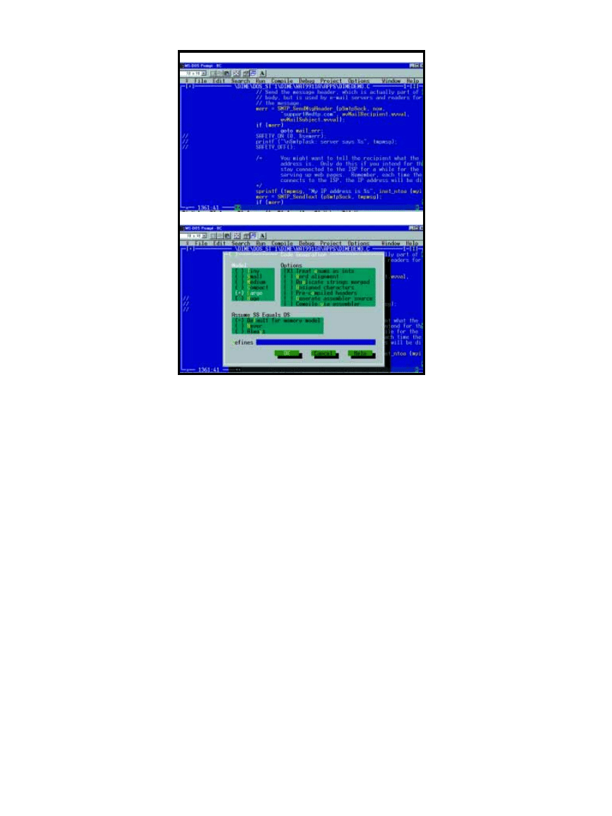
48
Issue 127 February 2001
CIRCUIT CELLAR
®
www.circuitcellar.com
DOSPPPD is a port of the
Linux PPPD program. The
original DOSPPPD has been
modified for automatic unat-
tended operation while run-
ning on the DOS Stamp. The
DOS Stamp version of
DOSPPPD is called DSPPPD.
DSPPPD differs from the
standard packet drivers in a
couple of ways. Normally,
packet drivers are physical
layer-oriented only. That is,
they perform only physical
layer functions. DSPPPD
works with the upper layers
of PPP such as LCP and IPCP
as well. And, DSPPPD shares
management of the physical
layer with the application.
UART is the only part of the
physical-layer DSPPPD that
uses commands. The rest of
the physical-layer functions
are controlled by the applica-
tion. The advantage of this
scheme is that you only
change the application to
accommodate different types of
modems or serial connections.
DSPPPD remains a constant.
On the DOS Stamp, DSPPPD
is a TSR (terminate and stay
resident) program that is in-
voked by the DOS command
line before the application is
kicked off. The command line
parameters are used to initialize
the UART. DSPPPD then goes
resident and waits for the appli-
cation. The application sends
the modem initialization string
to DSPPPD, which then passes
the string to the modem. The
application uses DSPPPD as the
courier between the modem and
application. For instance, the
application sends a modem
string to DSPPPD. DSPPPD
sends the modem string to the
modem. The modem responds
to the string and the application
queries DSPPPD for the status.
When a carrier is detected by
the modem and the application
via DSPPPD, the application
tells DSPPPD that the physical layer
is up and to begin the PPP process. If
all goes well through the Establish
and Authenticate phases, DSPPPD
will enter the Network phase and
inform the application that the IP
layer is up. It’s then up to the applica-
tion to transfer data and check the
integrity of the physical layer. If the
physical layer goes down, it is the
responsibility of the controlling appli-
cation to inform DSPPPD that the
physical layer is down. DSPPPD then
moves the PPP status to dead.
Now, let’s look at how a PPP link
is established using DSPPPD and the
DOS Stamp configured as a DIME.
SETTING THE STAGE
Before I jump into the Internet
wearing a DOS swimsuit, I’ve got to
prepare some Florida-room equipment
to handle the DOS Stamp program-
ming environment. Borland C++ 3.1
was written to work with Bill’s Win-
dows V.3.1. I really want to show you
the DIME’s Internet process by TV
rather than play-by-play radio. So, I
decided to try to load the Borland C
compiler into a WIN98 setup. This
b)
Photo 4a—
Twenty-four hours a day, seven days a week….
b—
It’s been a long
time since I’ve had to deal with this screen.
a)
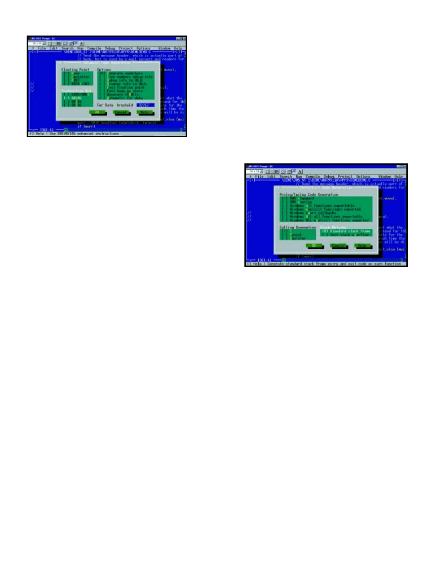
CIRCUIT CELLAR
®
Issue 127 February 2001
49
www.circuitcellar.com
way, I can capture the screens as I go
along. The Borland C++ 3.1 load con-
sists of 12 diskettes, and I’m hoping
they don’t have glitches. If the load
fails, I’ll move to V.4.0 and try it from
there. The problem is, Borland C++
4.0 is on 22 diskettes. Yikes!
As the Borland C++ 3.1 is loading,
I’ll tell you about some other goodies
that came with the DOS Stamp DIME
package. You’ve got to hook up the
DOS Stamp physically, and looking at
Photo 1, you could conclude that the
only way to do this is through the
header pins. The DOS Stamp comes
with a ribbon cable that is stripped out
to accommodate COM1, COM2, and
power. There’s also a crossover cable
to connect to the serial port of my PC.
Hooking up the 5-VDC wall wart,
you get the good news as shown in
Photo 2a. Ivan Baggett of Bagotronix, a
great help to me, also included some
utilities for the Disk-on-Chip, embed-
ded DOS-ROM, and DIME/uCII-
WATTCP. I got the Borland C++ 3.1
to come up in a WIN98 DOS window.
You’ll soon see if it actually works
there. Now that all of the prerequisite
software is loaded, let’s get DOS to
take us to the Internet.
I hooked up the modem supplied by
Bagotronix and snapped in my dial-up
line. First, you’re supposed to load
DSPPPD via the DOS command line,
but before you do that it may be wise
to see if you can compile a program
for the DOS Stamp. Photo 2b shows
an entry that is really my ISP’s phone
number. Because I would like to send
e-mail, an entry in the SMTP area
would be a good thing. The code in
Photo 3 shows that my mail carrier is
mail.digital.net. Now that my SMTP
mail server is defined, I’ll give the
program the data needed to
talk to the mail server. The
final address entry you see
in Photo 4a tells the SMTP
server who to send the
mail to. As you can see,
it’s a familiar address.
There’s still some work
to be done before you can
compile. The DIME user’s
manual asks that compiler
options be set with the
following attributes:
•
large memory model
•
no floating-point math
•
standard stack frame
•
no debugging info
•
80186 instructions
Photo 4b shows how
the Borland C++ 3.1 com-
piler takes care of the
memory model problem.
The next screenshot,
Photo 5, is multitalented.
Floating-point and instruc-
tion set requirements for
the DOS Stamp are satisfied on the
left side of the advanced code genera-
tion window. Bug spray is eliminated
on the right side of the window. All
that’s left on your compiler checklist
is the Stack setting, and that’s com-
pleted with an “X” in the appropriate
box in Photo 6.
After all of the compiler switches
are set, see if you can get a clean com-
pile and link running Borland C++ 3.1
under a WIN98 DOS window. Fortu-
nately, everything I knew years ago
came back and I finally got a good
Photo 5—
Notice there’s nothing for 80486 and above.
Photo 6—
Back then, I didn’t have a very good grasp of the DLL
concept. It was just like magic.
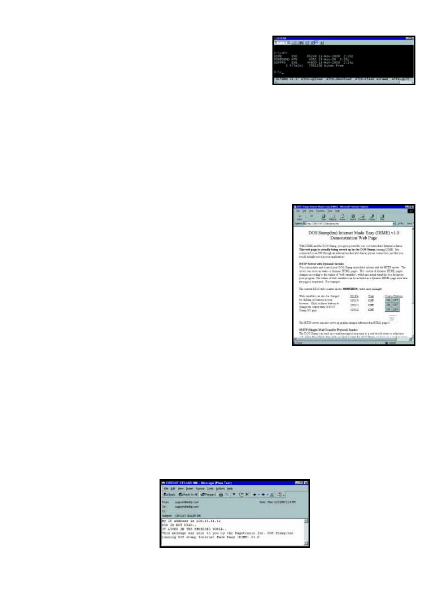
50
Issue 127 February 2001
CIRCUIT CELLAR
®
www.circuitcellar.com
Borland C++ 3.1 make file to
produce a usable
DIME.exe file.
The code for the make file is
shown in Listing 1. There was
some uCOS and DOS Stamp code
that needed to be linked to the
original code where I changed the
phone number and e-mail addresses
earlier. A separate
.CFG file holds all
of the compiler switch information,
which is accessed via pointers in the
DIME make file.
The next step is to get the execut-
able modules to the DOS Stamp vir-
tual disk space. That’s where XLTERM
comes in, it’s easier to use as far as
the DOS Stamp is concerned. To get
the
.exe files up to the DOS Stamp,
all I had to do was hot-key Alt+U and
enter the originating path. XLTERM
then moved the files up to the DOS
Stamp disk area you see in Photo 7.
Almost there. All that stands be-
tween you giving the command to dial
the phone is a single configuration file.
WATTCP must be configured before
you can open up and use the sockets.
The
WATTCP.CFG file is read by
WATTCP when the
sock_init()
function is called. Here’s what has to
be inside the
WATTCP.CFG file:
•
IP address assignment method
•
gateway IP address
•
net mask
•
name server IP address
I could have created this file some-
where else and uploaded it, but I de-
cided to create the
WATTCP.CFG file on
the DOS Stamp because it has full DOS
capabilities.
GATEWAY
I know that my ISP will dynami-
cally assign an IP address when I au-
thenticate. So, the first line of my
WATTCP.CFG file tells WATTCP that
I’ll get my IP address from the ISP via
DHCP. My ISP’s gateway address is
198.69.104.2. So, that’s my gateway
and I’m stickin’ to it. Because my
gateway address is a class C address,
it will need a class C subnetwork
mask, which will be 255.255.255.0.
Finally, I define my domain name
server (DNS), which happens to be
216.53.130.2. That should do it. Let’s
give it a whirl.
Remember that you must invoke
the DSPPPD TSR before you do any-
thing. So, I enter:
Dspppd 38400 local–crtscts
asyncmap a0000 user edtp passwd
xxxxxxx
I won’t show you this photo be-
cause I don’t want any of you writing
notes in my name! Trust me, the
positive acknowledgement to
the DSPPPD command line
entry reads: installed packet
driver handler at vector 0x60.
Next, I kicked off the
DIME.EXE file I modified
earlier. Just like Ivan said it
would, the modem came to
life. I heard a dial tone and
then 633-4710 toned out in
Photo 8—
You can also get this page served to you
by going to www.bagotronix.com.
Photo 9—
Pretty slick, and it’s done with DOS.
Photo 7—
Here is a directory of a no-spin hard disk.
CIRCUIT CELLAR
®
Issue 127 February 2001
51
www.circuitcellar.com
Fred Eady has more than 20 years of
experience as a systems engineer. He
has worked with computers and com-
munication systems large and small,
simple and complex. His forte is em-
bedded-systems design and communi-
cations. Fred may be reached at
fred@edtp.com.
SOURCES
DOS Stamp Internet Made Easy
(DIME)
Bagotronix Inc.
(850) 942-7905
Fax: (850) 942-7905
www.bagotronix.com
DS1689
Dallas Semiconductor
(972) 731-4448
Fax: (972) 371-3715
www.dalsemi.com
AM188ES CPU
Advanced Micro Devices
(408) 732-2400
(800) 538-8450
www.amd.com
MAX197
Maxim Integrated Products, Inc.
(408) 737-7600
(800) 998-8800
Fax: (408) 737-7194
www.maxim-ic.com
DTMF chords. Seconds later, I re-
ceived my ISP assigned IP address,
208.14.41.12. Turning to another PC
in the Florida room, I quickly brought
up an Internet Explorer browser and
entered the 208.14.41.12 IP address
followed by /dimedemo.htm. Again,
just as Ivan said, Photo 8 appeared.
The shot in Photo 8 is actually
being served via my ISP through the
Internet to my browser that’s con-
nected to the Road Runner service. In
addition, the HTML behind the
browser allows interaction with the
application program. That is, you can
actually use values you compute or
Listing 1—
I had to look at a few examples before the brain cells awakened from sleep mode.
.AUTODEPEND
.PATH.obj = C:\DIME
#
*Translator Definitions*
CC = bcc +DIME.CFG
TASM = TASM
TLIB = tlib
TLINK = tlink
LIBPATH = C:\BORLANDC\LIB;C:\DIME\LIB;C:\DIME\APPS
INCLUDEPATH =
C:\BORLANDC\INCLUDE;C:\DIME\INCLUDE;C:\DIME\APPS
#
*Implicit Rules*
.c.obj:
$(CC) -c {$< }
.cpp.obj:
$(CC) -c {$< }
#
*List Macros*
EXE_dependencies = \
dimedemo.obj
#
*Explicit Rules*
c:\dime\dime.exe: dime.cfg $(EXE_dependencies)
$(TLINK) /x/c/P-/L$(LIBPATH) @&&|
c0l.obj+
c:\dime\dimedemo.obj
c:\dime\dime
# no map file
cl.lib
|
#
*Individual File Dependencies*
dimedemo.obj: dime.cfg apps\dimedemo.c
$(CC) -c apps\dimedemo.c
#
*Compiler Configuration File*
dime.cfg: dime.mak
copy &&|
-ml
-1
-f-
-ff-
-vi-
-wpro
-weas
-wpre
-nC:\DIME
-I$(INCLUDEPATH)
-L$(LIBPATH)
-P-.C
| dime.cfg
acquire to make up the HTML that’s
served from the DOS Stamp. Pretty
clever for a tiny CPU complex that
runs on DOS, don’t you think?
I’m an e-mail junkie. I love getting
it and I love sending it. So, I had to try
out the e-mail capabilities of the DOS
Stamp in DIME mode. Photo 9 is an
actual note sent from the served web
page you see in Photo 8.
DOS IS NOT DEAD…
It lives in the embedded world.
With help from the uCOSII RTOS and
WATTCP, the DOS Stamp becomes a
formidable Internet tool. I have sim-
ply scratched the surface about
Internet capability that can be found
in the DOS Stamp’s hardware and
software. Not only is the hardware
good, the documentation that Ivan
and crew include with the DOS
Stamp is well laid out and informa-
tive. If you know nothing about how
the Internet works, you should get
your own DIME and documentation.
Reading the excellent documentation
and performing the hardware tasks
will give you a good understanding of
how to do it on the ’Net. The best
thing about the DIME is that if you
know DOS and a little bit of C, you’re
pretty much guaranteed success.
Oh, yeah. I never explained the
“M” and “E” in DIME. Those last
letters stand for “made easy.” Trans-
lation: It doesn’t have to be compli-
cated to be embedded.
I
52
Issue 127 February 2001
CIRCUIT CELLAR
®
www.circuitcellar.com
Part
2
3
Fundamentals of
Second-Order Systems
MICRO
SERIES
David Tweed
w
If you dig
equations
then you’ll
enjoy this article. If
understanding how
mathematical tools
affect second-order
systems is a source
of much headscratch-
ing for you, dig in and
enjoy the insight
Dave offers here.
elcome to Part
2. I’m presenting
some of the common
theoretical background
and mathematical tools for many of
the dynamic systems found in all
branches of engineering. These include
filters of various types and servo-
mechanisms such as phase-locked
loops and robotic positioners.
Part 1 covered the basic setup of
both mechanical and electrical second-
order systems. The former consists of a
mass, spring, and damper, and the lat-
ter consists of a coil, capacitor, and
resistor. Every quantity in each system
has an analogue in the other, and the
same math is used to describe both
systems. A simple numerical simula-
tion was also set up.
Now it’s time to take a deeper look
at the underlying mathematics and
derive more powerful ways of describ-
ing such systems. We’ll take a look at
how these systems can be used as fil-
ters, and then what happens when
negative feedback is added to the sys-
tem, as in servomechanisms.
I’m not going to spend a lot of time
talking about the Mathcad simula-
tions, but there are files that you can
download and play with for most of
the figures in this installment.
MATHEMATICAL MODEL
The mathematical formulae you
built so far are just stepwise numerical
simulations. But, what about a closed-
form, continuous solution? It turns out
not to be too difficult, and involves
only a little calculus. Bear with me and
we’ll get through it quickly.
Start by listing the constraints of
the components and constraints arising
from how they’re connected. The coil
develops a voltage in proportion to its
inductance and the time derivative of
the current through it:
The capacitor carries a current that is
proportional to its capacitance and the
time derivative of the voltage across it:
Or equivalently, the capacitor voltage
is the integral of the current through it
divided by the capacitance:
The resistor develops a voltage in
proportion to its resistance and the
current through it:
V
res
= R × I
The current, I, is the same every-
where in the circuit.
The voltages must sum to zero
around the circuit:
V
cap
+ V
res
+ V
coil
= 0
Or, after making these substitutions:
This final equation is the basic second-
order problem. If both sides of it are
differentiated once with respect to
time, you get a linear, second-order
homogeneous, differential equation:
Solving such equations is difficult.
However, note that here you need a
function that, when added to its first
and second derivatives, sums to zero.
Part 2: The Tools of the Trade
2
3
of
CIRCUIT CELLAR
®
Issue 127 February 2001
53
www.circuitcellar.com
The solution probably will be an expo-
nential function. Let’s try:
i(t) = Ae
st
The first and second derivatives are:
Making the substitutions, the differen-
tial equation becomes:
Solving this requires that the third
factor in parentheses be set to zero.
Because this is a quadratic equation,
there are two solutions:
By defining a couple of new constants,
you can write a simpler form:
α
is the damping coefficient, and
ω
0
is
the resonant frequency. In general,
ω
is used to denote a radian frequency,
which is related to a frequency f in
hertz by a factor of 2
π
. I’m going to
stick with radian frequency to keep
the formulae simple; if you want to
convert to hertz, just use the relation:
You’ll also find it useful to define the
damping ratio:
Look at the argument to the square
root: If this quantity is negative, then
the square root is an imaginary number
and the solution s is going to be a
conjugate pair of complex numbers. In
real terms, this means that the decay is
periodic. If it’s exactly zero, then the
circuit is said to be critically damped.
And if the quantity is positive, there
will be two real values of s in the
solution and the decay will be aperi-
odic. These three cases correspond to
the quantity
ζ
being less than, ex-
actly, and greater than 1, respectively.
It can be useful to
solve this expression
for how R relates to L
and C (see initial qua-
dratic solution):
• if R
2
= 4L/C, the
circuit is critically
damped
• if R
2
≥
4L/C, the
decay is aperiodic
• if R
2
< 4L/C, the
decay is periodic
The full form of the
solution can be written out
like this:
A
1
and A
2
are picked to
satisfy whatever initial
conditions are set up for
the circuit. If s
1
and s
2
are
two different real values,
the overall function is the
sum of two exponential
equations with two differ-
ent time constants.
In general, you’ll find
that A
1
and A
2
have equal values but
opposite signs, so you end up with a
function that is zero at t = 0 and at t =
infinity (see Figure 1a).
If s
1
and s
2
are a complex conjugate
pair, you can define a different fre-
quency, the natural frequency:
And, this allows you to write the solu-
tion as:
Euler’s Identity says:
E
jKt
= cos Kt + j sin Kt
Remembering that A
1
= –A
2
, you
find that the cosine terms cancel and
you’re left with an expression that
describes a decaying sinewave:
i(t) = 2A
1
e
–
α
t
j sin (
ω
Nt)
Figure 1a—
The aperiodic response of an overdamped, second-
order system consists of the difference between two exponential
decays.
b—
The periodic response of an underdamped, second-
order system consists of a sinewave with an exponentially
decaying amplitude.
Figure 2a—
A sinewave can be characterized by its amplitude and phase angle, or
equivalently, by the magnitudes of its in-phase (sine) and quadrature (cosine)
components. This vector can represent any sinewave quantity at a particular
frequency.
b—
Current is in phase with the applied voltage in a resistor, but it lags
by 90° in a coil and leads by 90° in a capacitor.
0.5
0.4
0.3
0.2
0.1
0
0
0.5
1
1.5
2
2.5
3
3.5
4
Time (s)
Current (amps)
Time (s)
Current (amps)
0
1
2
3
4
5
6
7
8
9 10 11 12 13 14
1
0.8
0.6
0.4
–1
–0.8
–0.6
–0.4
0.2
–0.2
0
a)
b)
+90˚
Quadrature
component
(cosine)
±180˚
Phase angle
In-phase
component
(sine)
–90˚
0˚
Amplitude
+90˚
C current
L current
Applied voltage
–90˚
0˚
R current
a)
b)

54
Issue 127 February 2001
CIRCUIT CELLAR
®
www.circuitcellar.com
+90˚
V
L
–90˚
0˚
V
R
V
C
I
Overall
sum
θ
forced response must be a sinewave at
the same frequency, but with a differ-
ent amplitude and/or phase.
Together these facts mean that if
you understand the response of a cir-
cuit or system to sinewaves of various
frequencies, you always can get the
response to arbitrary periodic forcing
functions. Any sinewave is character-
ized by just two parameters, its am-
plitude and initial phase. Together,
these parameters can be thought of as
a vector in phase space, also known as
a phasor (see Figure 2a).
Amplitude can be in units of any
physical quantity. This can let you
show the relationship between volt-
age and current for your components
(see Figure 2b). In the resistor, the
current always is in phase with the
applied voltage; or, if you apply a
current, the voltage is always in phase
with that. The relationship between
voltage and frequency is independent
of the frequency.
In the coil, the current always lags
the voltage by 90°, or equivalently,
the voltage leads the current by 90°.
did a simulation last
month, now it’s time
to derive the math
that describes this
aspect of the system.
This requires a
different set of math
tools from those used
so far. Here, phasors
and complex imped-
ances rule the day,
but first let me get a
few basic concepts
out of the way.
Remember that
the fast Fourier trans-
form shows that any periodic forcing
function can be expressed as a sum of
sines and cosines, or equivalently, as
a sum of sines whose relative phase
can be varied. Because you’re dealing
with strictly linear circuits here, you
can use the principle of superposition
to analyze the circuit response one
sinewave component at a time. And
you can derive the overall response by
summing the components at the end.
Also, because of the linearity, the
Figure 1b shows an example of this
type of response.
The Mathcad sheet for Figure 1 lets
you plug in values for R, L, and C to
see the effect on
α
,
ω
0
,
ω
N
, and
ζ
.
DRIVEN RESPONSE
This information provides insight
into the basic mechanisms of second-
order systems, but you’re probably
more interested in the response of the
system to periodic driving forces. You
Figure 3a—
Here’s the RLC circuit with a current source added in series.
To find the total voltage, the component voltages must be added
vectorially by placing the individual vectors end-to-end.
b—
At frequencies below
resonance, the capacitive component is larger than the inductive component,
resulting in an overall negative phase shift
θ
.
c—
At frequencies above reso-
nance, the overall phase shift
θ
is positive.
a)
V
L
+
–
V
C
+
–
V
R
+
–
I
+90˚
V
L
–90˚
0˚
V
R
V
C
I
Overall
sum
θ
c)
b)
CIRCUIT CELLAR
®
Issue 127 February 2001
55
www.circuitcellar.com
However, their magnitudes are related
by a function that depends on fre-
quency. If the voltage is held con-
stant, then the current decreases with
increasing frequency, or if the current
is held constant, the voltage increases
with increasing frequency. Because
impedance is defined to be the ratio of
voltage to current, the last statement
is the same as saying the impedance
of the coil increases with frequency.
Everything is reversed for the ca-
pacitor. Thus, the voltage always lags
the current by 90°, or equivalently,
the current leads the voltage by 90°.
Again though, their magnitudes are
related by a function that depends on
frequency. However, now, if the volt-
age is held constant, the current esca-
lates with increasing frequency, or if
the current is held constant, the volt-
age (and impedance) decreases with
increasing frequency.
Look at Figure 3a.
Because the current
is the same every-
where in a series
circuit, each of the
components has a
voltage across it
determined by the
effect of the current
on that component.
The voltage across
the current source is
the sum of the three
component voltages.
Figure 3b shows
how they add up. Because the voltages
are at different phase angles, use vec-
tor addition to add them. The fre-
quency of the current source is less
than the resonant frequency of the
circuit. The capacitor’s voltage is
greater than the coil’s voltage, so the
overall sum has a phase angle that’s
negative with respect to the current
source (which is arbitrarily set at 0°
for simplicity).
As the frequency is decreased fur-
ther, the C component continues to
grow while the L component shrinks,
causing the total vector to lengthen
and the phase angle to increase. In the
limit, the vector is infinitely long and
parallel to the –90° axis. This corre-
sponds to a DC current source charg-
ing the capacitor indefinitely.
Figure 3c shows the case where the
source frequency is greater than the
resonant frequency. Now, the coil’s
Figure 5a—
The sum of the R and L voltage components produces a high-pass filter function.
b—
The output voltage
and phase angle are given by the vector showing the partial sum of the R and L components.
c—
When the magni-
tude and angle of the R + L vector is plotted against frequency, you see the high-pass function.
a)
c)
b)
+90˚
V
OUT
–90˚
0˚
V
IN
A
B
C
D
E
V
IN
+
–
V
L
+
–
V
OUT
=
V
R
+ V
L
V
C
+
–
V
R
+
–
0
10
20
30
40
50
60
70
80
90
100
2.5
2
1.5
1
0.5
0
Radian frequency (1/s)
Amplitude (v
olts)
0
10
20
30
40
50
60
70
80
90
100
150
100
50
0
Radian frequency (1/s)
Phase angle (deg
rees)
Figure 4a—
If the current source is replaced by a voltage source, the
component relationships remain the same, but the diagrams must be
rotated to put the overall voltage on the 0° axis.
b—
Below resonance, the current
has a positive phase shift
θ
relative to the applied voltage.
c—
At a lower fre-
quency, the current is smaller and the phase shift
θ
is greater.
a)
c)
b)
+90˚
V
L
–90˚
0˚
V
R
V
C
θ
Overall
sum
θ
+90˚
V
L
–90˚
0˚
V
R
V
C
θ
Overall
sum
θ
V
IN
+
–
V
L
+
–
V
C
+
–
V
R
+
–
–
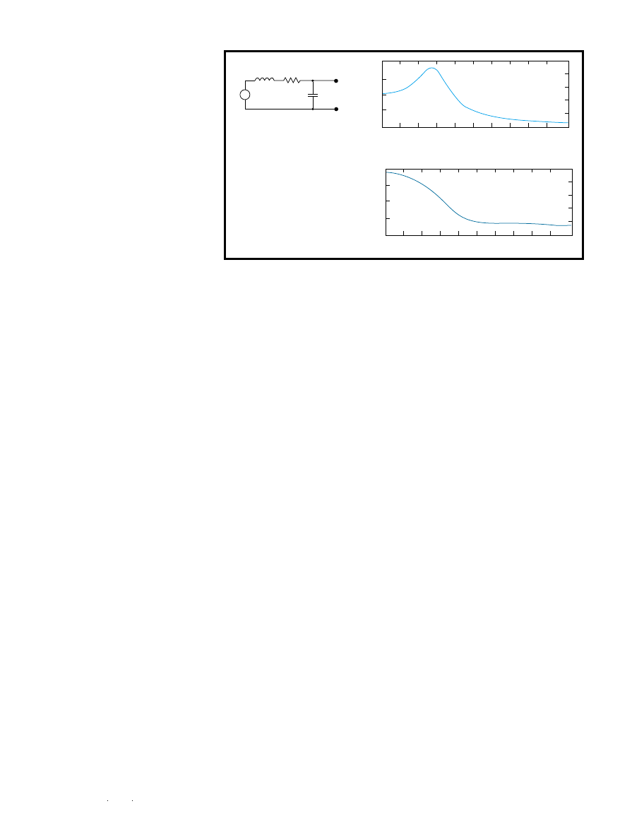
V
IN
+
–
V
C
+
–
V
OUT
=V
C
V
L
V
R
+
+
–
–
0
10
20
30
40
50
60
70
80
90
100
2.5
1.5
1
0.5
0
Radian frequency (1/s)
Amplitude (v
olts)
0
10
20
30
40
50
60
70
80
90
100
0
–50
–100
–150
0
Radian frequency (1/s)
Phase angle (deg
rees)
a)
b)
Figure 6a—
Swapping the R
and L with the C produces a
low-pass filter function.
b—
The
magnitude of the C vector is
the complement of the high-
pass response, and the phase
angles have the opposite
values.
voltage component is greater than the
capacitor’s component (i.e., the coil’s
impedance is greater than the
capacitor’s, because the current is the
same in both) and the phase angle of
the sum is positive. If the frequency
continues to increase, both the phase
angle and amplitude increase, as well.
As you might have guessed, the
resonant case is the frequency at
which the voltage (and impedance) of
the coil and capacitor cancel each
other, leaving only the resistive com-
ponent in the sum. At this point, the
total voltage is at a minimum and the
phase angle is 0°, which means that the
voltage is in phase with the current.
What happens if a voltage source is
substituted for the current source (see
Figure 4a)? Well, you have the same
sum of voltages as before, but now the
total voltage is constrained to match
that of the voltage source and the
current phase angle and magnitude are
free to vary.
Figure 4b shows what happens
when Figure 3b is rotated so that the
sum voltage lies along the 0° axis,
scaled so that the length of this vector
corresponds to the applied voltage.
The current is still the same every-
where in the circuit, and because it is
in phase with and proportional to the
voltage across the resistor, just look at
the resistive component of the voltage
diagram to see what it is.
The Mathcad sheet for Figures 3
and 4 lets you to plug in various val-
ues for R, L, C, and
ω
to see the effect
on the various component vectors.
SECOND-ORDER FILTERS
Second-order systems can be used as
filters of various types. As you saw, the
series RLC circuit has a notch in its
voltage response when driven with a
current source and a peak in its current
response when driven with a voltage
source. This gives basic band-stop and
band-pass capabilities, but what about
high-pass and low-pass functions?
Start by redrawing the circuit of Fig-
ure 4a (see Figure 5a), and take a look
at the sum of the resistive and induc-
tive components of the response. This
is simply a matter of drawing an addi-
tional vector in the phase sketch, as
shown in Figure 5b, which shows the
R + L component for several different
frequencies.
The curved, dotted line shows the
locus of points reached by this vector
for a wide range of frequencies. Note
that
ω
0
corresponds to point C on this
curve, but this isn’t where the V
OUT
vector is the longest, which actually
occurs at point D. Point D corre-
sponds to the
ω
N
calculated earlier.
Figure 5c shows the length (magni-
tude) and direction (phase angle) of
the R + L vector plotted as a function
of frequency. And sure enough, it
looks like a high-pass filter.
Go back to the physical mass-
spring-damper system, where the
spring corresponds to the capacitor,
the mass to the coil, and the damper
to the resistor. Recall that current in
the electrical system corresponds to
the motion of the mass (relative to
the anchor point) in the physical sys-

CIRCUIT CELLAR
®
Issue 127 February 2001
59
www.circuitcellar.com
RESOURCE
W. Hayt, Jr., and J. Kemmerly, Engi-
neering Circuit Analysis (McGraw
Hill Series in Electrical and Computer
Engineering)
, McGraw-Hill Higher
Education, Burr Ridge, IL, 1978.
SOURCE
Mathcad
Mathsoft, Inc.
(617) 577-1017 Fax: (617) 577-8829
www.mathsoft.com
Dave Tweed is an independent con-
sultant. He has been developing hard-
ware and real-time software for
microprocessors for many years. His
system design experience includes
computer design from supercomput-
ers to workstations, digital telecom-
munications systems, and the appli-
cation of embedded microcomputers
and DSPs. You may reach him at
dtweed@acm.org.
tem and that voltage corresponds to
physical force. The AC voltage source
in the electrical system is equivalent
to a cyclical mechanical force applied
to the anchor point of the mechanical
system (which is free to move).
If the cyclical frequency is high,
the mass tends to sit still because of
its inertia. The output voltage of the
electrical system is equivalent to the
total mechanical force across the
damper and the net force on the mass.
The damper resists high-speed mo-
tion, so it couples most of the input
force directly to the mass, and the
anchor point moves very little. This
means that there is insignificant force
across the spring, which requires a
strong physical motion of one end or
the other to develop significant force.
Any motion of the mass and anchor
point will be in phase with each other
and with the applied force.
If the cyclical frequency is low, the
mass moves in response to the forces
on it, and because the damper provides
little resistance to this low-velocity
motion, most of this force is coupled
by the spring. The anchor point moves
as well, and the magnitude of the mo-
tion of the mass relative to the anchor
point (corresponding to current) is
small. The damper plus mass force (the
analog of the electrical output voltage)
is negligible.
The low-pass function is con-
structed by realizing that whatever
input voltage doesn’t appear across
the R-L combination must be across
the C. So, if the R-L combination is
swapped with the C (see Figure 6a),
you get the inverse response shown in
Figure 6b. You can do the same sort of
vector analysis for the high-pass filter,
but then the output vector is the same
as the C component alone.
UNTIL NEXT TIME
Now you’ve seen some of the math
that describes the transient behavior
and steady state of second-order sys-
tems. If you’d like to learn more, read
the book listed in the Resources. It
covers the topic with more detail and
rigor, but in a very readable way.
Next month, I’ll talk about active
second-order systems and then move
onto the topic of servomechanisms.
I
60
Issue 127 February 2001
CIRCUIT CELLAR
®
www.circuitcellar.com
Diagnostics
HVAC
Charging
Electric
traction
motor or
internal
combustion
engine
Transmission
Cruise
Steeling
Dash
ABS
Fuel sensors
Fuel
pump
Auto
belt
Ride
control
Keyless entry
Wipers
Security
Memory
seat
Air
bag
Entertainment
Windows
Mirrors
Climate
Navigation
t
he Ethernet in
office automation
is analogous to the
CAN (controller area
network) in automotive applications.
The CAN bus system has penetrated
the automotive market and found its
way into other industrial applications.
These applications require a robust
protocol for communications because
most of the CAN nodes are located in a
noisy environment.
But, the CAN bus can be complex as
well as expensive to implement. So,
European automotive manufacturers
have defined a new protocol called the
LIN (local interconnect network)
protocol standard. This bus is a low-
cost, logical connection to the CAN
bus gateway and its implementation.
In a car, some nodes do not require
high-speed communications. For low-
speed communications, manufacturers
use different field bus systems. Because
these bus implementations are not
compatible, high redesign and main-
tenance costs often result. Tools for
support of the different buses created
problems, motivating European
manufacturers to develop the new LIN
bus protocol. The cost of a LIN is
significantly less than for a CAN node.
THE AUTOMOBILE NETWORK
The automobile network is broken
up into subnetworks—body control,
power train, door nodes, and so on (see
Figure 1). The power train and body
control both are CAN networks, and
door nodes are based on the LIN bus.
Because door nodes react slowly, the
maximum transmission rate for the
LIN bus is 20 Kbps, which translates
into a bit time of approximately 50 µs.
The LIN bus is a single master,
multi-slave bus that communicates on
a single-wire bus. The protocol is self-
synchronizing, allowing the slave
nodes to run from an RC oscillator.
The master transmits to the slaves,
but the slaves transmit only when
asked by the master, with one excep-
tion, when they want to issue a wake-
FEATURE
ARTICLE
Thomas Schmidt
If you’ve peeked un-
der the skin of a late-
model vehicle, you
know that there are
more than a few
inches of network
wiring that keeps ev-
erything running. The
environment presents
quite a challenge for
maintaining reliable
communications.
Enhancing Automotive
Subsystem Design with LIN
Implementing a LIN Protocol-to-CAN
Gateway
Figure 1—
Take a look at this automotive network that consists of small subnetworks like the LIN bus
network. The communication between the LIN bus and CAN bus networks is done via gateways.
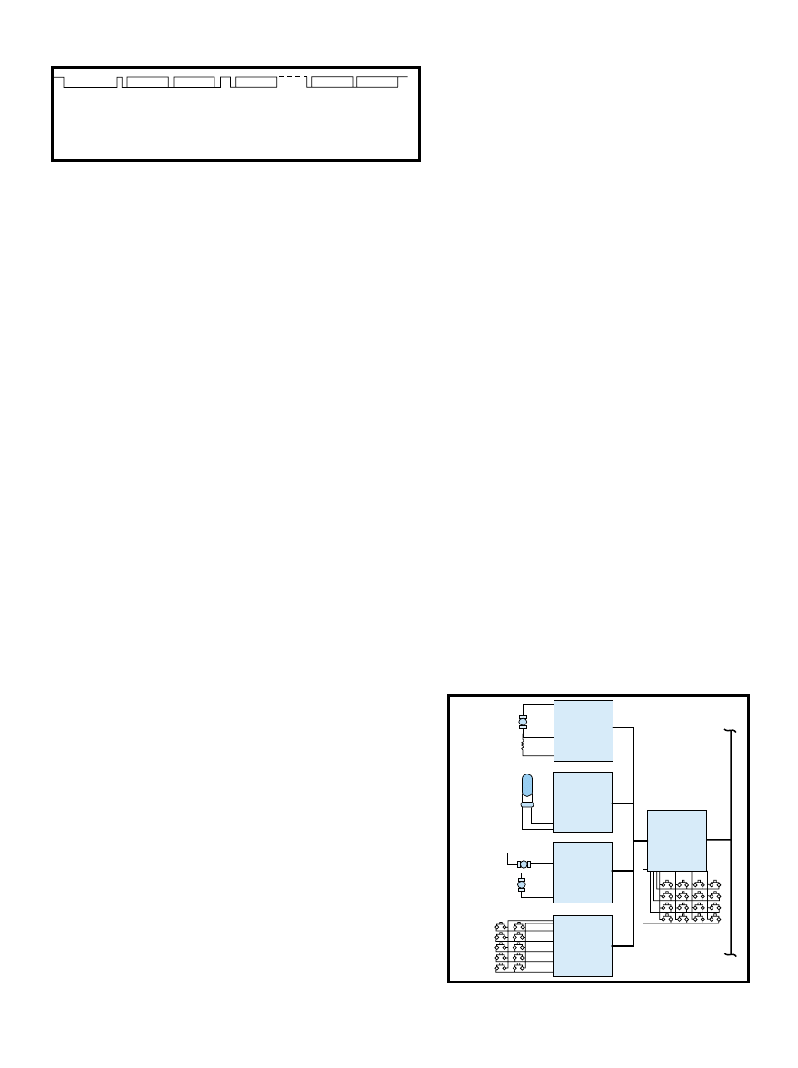
CIRCUIT CELLAR
®
Issue 127 February 2001
61
www.circuitcellar.com
up signal. The slave nodes identify
their messages by the identifier bits,
meaning that several nodes can receive
the same message (see Figure 2).
The standard data frame contains a
synchronization break that initiates
the communications process and is
followed by a synchronization delim-
iter of 1 to 4 T
bit
(1 T
bit
is the transmis-
sion time for 1 bit). After that, the
synchronization field is transmitted.
The purpose of the synchronization
field is to adjust the data rate to the
transmitted signal. After the synchro-
nization field is transmitted, the iden-
tifier field, which includes the
identifier bits and two parity bits, is
initiated. The latter are calculated for
the identifier field. The former tell the
slaves what to do with the data and
determine if the data is relevant. Other
identifier bits can designate the data as
calibration data. After the identifier
field is sent, either the slave node re-
sponds to the message or the master
keeps transmitting data.
The next stop is a look at the data
fields. The data frame ends with a
checksum, which is calculated over all
data bytes (not including the identi-
fier byte or sync field) using Modulo
256 calculation.
The LIN bus master also uses the
sleep frame, which puts the bus and its
nodes into a low-power mode. The
sleep frame basically looks like a data
frame, except that the identifier field
contains the value 0x80. When initial-
izing the sleep frame, you must trans-
mit data following the identifier field.
The bus gets out of the sleep mode
when a wake-up signal is sent by the
master or any slave.
When the master or a slave wants to
send a wake-up signal, it transmits
value 0x80 followed by a 4- to 64-T
bit
wake-up delimiter. Then, the master
sends a data frame. If the master fails
to transmit the synchronization break
after 128 T
bit
,
a new wake-
up signal is
sent. This
procedure
does not
exceed three
attempts.
THE LIN-CAN GATEWAY
The LIN-CAN gate has to perform
six tasks. It must receive the CAN
message and convert it to a LIN
message. Then, it decodes the CAN
identifier for the LIN identifier,
transmits the message to LIN nodes,
and reads data from the LIN node.
Lastly, it sends data from the LIN node
to a CAN message and transmits it.
The LIN-CAN gateway’s center-
piece is the PIC18C658 (see Figure 3).
It has an integrated CAN module and
several other peripherals. The receive-
and-transmit pins of the CAN
controller are connected to an 82C251
CAN transceiver that is hooked up to
the CAN network.
On the other side, the receive-and-
transmit pins of the USART are
connected to a Si9243 K-line driver,
which is the physical interface to the
LIN bus slave nodes. The LIN bus runs
off a 12-V power supply and the CAN
bus runs off a 5-V differential bus. The
microcontroller performs the primary
functions of the LIN CAN gateway.
An alternative solution is to use a
MCP2510 stand-alone
CAN controller with a
PIC16F873. The latter
directs communications
to the LIN bus and
controller, which handles
the communications. The
PIC16F873 communicates
via an SPI interface to the
MCP2510. The MCP2510
is connected to an
82C251 CAN transceiver
chip, which is basically
the physical interface to
the CAN bus.
On the LIN-bus side, a
Si9243 K-line driver is
used. The task performed
by the gateway can be
broken up into three
functional blocks—CAN
communication, data conversion and
data link, and LIN communication.
The CAN module of the PIC18C658
handles most of the CAN com-
munications (see Figure 4).
The CAN bus module consists of
the message-buffering unit and
protocol engine. The latter handles all
functions for transmitting and
receiving messages on the CAN bus.
Any message detected on the CAN bus
is checked for errors and then matched
against filters to determine if it should
be received and stored in one of the
two receive registers. The CAN
module supports standard data,
extended data, remote, error, overload,
and interframe space frames.
The message acceptance filters and
masks determine if a message in the
message assembly buffer should be
loaded into either of the receive
buffers. After the message assembly
buffer receives a valid message, the
identifier fields of the message are
compared to the filter values and an
interrupt is generated.
If there is a match, the message will
be loaded into the appropriate receive
buffer. The filter masks determine
which bits in the identifier fields are
compared to the filters. A truth table is
referenced to indicate how each bit in
the identifier is compared to the masks
and filters to determine if the message
should be loaded into a receive buffer.
The mask bit determines which bits to
Sync field
Identifier field
Interfr
ame response
Sync break
Sync delimiter
Data field 1
Data field 8 Checksum field
Figure 2—
The typical LIN bus data frame can be initiated by the LIN bus master. The
master or slave sends the data bytes. The master always sends the synchronization
break signal, synchronization delimiter, synchronization field, and identifier field.
PIC18C658
or
PI16F877 &
MCP2510
18-pin Micro-
controller
18-pin Micro-
controller
18-pin Micro-
controller
8-pin Micro-
controller
6 × 2 Key
matrix
Side view
mirror
motors
Door lock
actuator
Current
sense
Window
motor
Door control
panel
CAN b
u
s
LIN b
u
s
Figure 3
—
The LIN-CAN bus gateway is shown here. Communication
among the buses is handled by a PIC18C658 microcontroller.
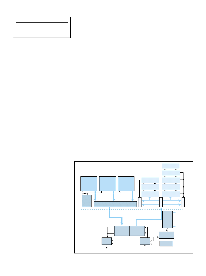
62
Issue 127 February 2001
CIRCUIT CELLAR
®
www.circuitcellar.com
it. For example, the LIN bus runs at
19.2 Kbps, where T
bit
= 52 µs. A synch-
ronization signal of 13 T
bit
has a
duration of 677 µs. Dividing this num-
ber by eight gives the bit time for the
synchronization signal, making the
data rate 11.8 Kbps. With the USART
transmit register loaded with 0x00,
transmitting this value at 11.8 Kbps
gives a synchronization signal of 13 T
bit
for a 19.2-Kbps network.
After the synchronization signal is
transmitted, the LIN-CAN gateway
sends the synchronization field,
allowing the slave nodes to adjust their
data rate using the field. After synch-
ronizing the slave nodes, the LIN-CAN
gateway sends the identifier field,
which contains the ID for the door
node and parity bits. The identifier
bits tell the door node controller to
open the door. If the command closed
it, it would mean the body controller
and LIN-CAN gateway had issued a
different appropriate identifier.
IMPLEMENTATION
There are different ways to
implement a slave node. One is when
the slave communicates via the
USART to the master. This requires a
stable oscillator frequency, because a
USART depends on an accurate input
oscillator frequency. Because most LIN
bus slave nodes perform easy tasks
such as reading a sensor or driving a
motor, small microcontrollers without
a USART are used. If a USART isn’t
available, slave communication has to
be implemented in the software.
In the following example, software
implementation is discussed for the
PIC12C672 microcontroller. After the
slave detects a falling edge on the GP2
pin, the software starts measuring time
for the synchronization break signal.
The measured time determines
whether this is a bus wake-up or
normal synchronization break signal. A
software counter measures the time. It
also generates the data rate for
receiving or transmitting data later.
TMR0 of the PIC12C672 is the system
clock and generates a time-out base
during the LIN bus communication.
After the sync break is measured,
the LIN bus master transmits the
synchronization field. The purpose of
this field is to synchronize the data
rate between the master and slave
controllers. The slave software counts
for five rising edges while the
transmission time is measured. Five
rising edges are equivalent to 8 bits of
data; so, the time measured equals the
transmission time for 8 bits.
MSGREQ
TXABT
TXLARB
TXERR
MTXB
UFF
Message
MSGREQ
TXABT
TXLARB
TXERR
MTXB
UFF
Message
MSGREQ
TXABT
TXLARB
TXERR
MTXB
UFF
Message
Acceptance mask
RXM0
Acceptance filter
RXF0
Acceptance filter
RXF1
Acceptance filter
RXF2
Acceptance filter
RXF3
Acceptance filter
RXF4
Acceptance filter
RXF5
Message
queue
control
R
X
B
0
R
X
B
1
M
A
B
Transmit shift
Receive shift
CRC generator
CRC check
Transmit byte sequencer
Receive
error
counter
Transmit
error
counter
Protocol finite
state machine
Transmit
logic
Bit-timing
logic
Bit-timing
generator
Acceptance mask
RXF1
Buffers
Protocol
engine
TX-pin
RX-pin
Data field
Identifier
Data field
Identifier
A
c
c
e
p
t
A
c
c
e
p
t
RXERRCNT
TXERRCNT
TXB0
TXB1
TXB2
Figure 4—
The CAN module consists of two blocks, the CAN protocol engine and buffers. The buffers
are the user interface to the CAN protocol engine.
ID4 ID5
Data length
00
2 bytes
01
2 bytes
10
4 bytes
11
8 bytes
Table 1—
This table states the decoding of the data
length. Bits ID4 and ID5 are located in the identifier
byte. The LIN bus master sends the identifier byte.
apply to the filter. If any mask bit is set
to zero, that bit will automatically be
accepted regardless of the filter bit.
The acceptance filter looks at
incoming messages for the IDE bit to
decide how to compare the identifiers.
The IDE bit in the CAN message tells
the CAN node if the message is using a
standard or extended identifier. If the
IDE bit is 0, the message is a standard
frame, and only standard identifier
filters are compared. If the IDE bit is 1,
the message is an extended frame, and
only filters with the extended
identifier are compared.
The receive buffer contains the data
bytes of the CAN message. In order to
find out which identifier was used for
the message, the filter-hit bits have to
be read. The identifier bits of the CAN
message determine which identifier
field will be sent to the LIN bus.
After the microcontroller receives
the message, the LIN-CAN gateway
determines for which node the message
is meant because there are many LIN
nodes connected to the LIN bus
network (see Figure 1). The firmware
does this by decoding the identifier
field and using a look-up table.
Three look-up tables are required for
a standard 21-bit identifier. The table
results determine which node has to be
addressed in the LIN bus network. If
only the lower 8 bits have to be con-
sidered, one look-up table is sufficient.
After the correct identifier for the
LIN node is found, the LIN-CAN
gateway transmits the synchronization
break. To accomplish this while this
signal is being transmitted, the LIN-
CAN gateway firmware calculates the
parity bits for the LIN bus identifier
field. For LIN bus communication, the
USART of the PIC18C658 is used.
The synchronization signal of the
LIN bus is 13 T
bit
. The USART is
configured to a slower data rate than
the standard LIN bus rate to generate

CIRCUIT CELLAR
®
Issue 127 February 2001
65
www.circuitcellar.com
SOURCES
SPI
Motorola, Inc.
(602) 952-4103
Fax: (602) 952-4067
www.mot-sps.com/sps/general/
Thomas Schmidt is senior automotive
application engineer for Microchip
Technology. He graduated in 1994
from the Fachhochschule Ostfriesland
in Germany. You may reach him at
thomas.schmidt@microchip.com
.
After measuring the time for 8 bits,
the transmission time for one bit has
to be calculated by shifting the timer
register of the software counter four
times. The counter register is 16-bits
wide in order to ensure that the
PIC12C672 can support all the LIN bus
committee proposed data rates—2400,
4800, 9600, 19.2 Kbps. In this example,
the PIC12C672 runs on the 4-MHz
internal RC oscillator, which is
sufficient to support all recommended
data rates.
After dividing the counter register
by eight, the slave receives the
identifier byte. This byte tells the
slave to receive more data, transmit
data, or ignore the message. The
sampling for the receiving data is
generated with a software counter. The
software counter uses the calculated
value from the previous reception
(synchronization field).
After the identifier byte is received,
the slave determines if data has to be
transmitted, received, or ignored by
decoding the identifier bits using a
look-up table. Decoding takes two
steps because the LIN bus specification
breaks the identifier into four groups
of 16 identifiers.
The four groups are determined by
data bits ID4 and ID5. ID0 to ID4 are
the identifier bits. First determine
which group has to be decoded. Then,
the identifier bytes are decoded. Now
decoding means setting the slave into
Receive, Transmit, or Ignore mode. No
action is taken at this point.
After the slave decodes the
identifier bits, you must determine the
length of the message to receive or
transmit. You can determine the data
length by decoding the ID4 and ID5
bits in the identifier byte (see Table 1).
After the slave node knows how
many data bytes have to be transmit-
ted or received, the slave goes into
either transmit or receive mode. After
communicating, the slave takes action
upon the identifier. During the com-
munication process, the controller can
be interrupted to do other things. En-
sure that the data rate doesn’t change.
So, now you know the details about
LIN. And, you understand its benefits;
not only does LIN work as a logical
connection to the CAN bus gateway, it
also costs less than the CAN node.
This, of course, helps the automotive
and industrial markets, which rely on
the CAN bus system.
I
- Xilinx CPLD
- Xilinx CPLD
- Xilinx CPLD
- Xilinx CPLD
- Xilinx CPLD
- 5V DC Power
- 5V DC Power
- 5V DC Power
- 5V DC Power
- 5V DC Power
- Clock/Calender
- Clock/Calender
- Clock/Calender
- Clock/Calender
- Clock/Calender
- RS232, RS485
- RS232, RS485
- RS232, RS485
- RS232, RS485
- RS232, RS485
- Dimensions 4.2" x 3.6"
- Dimensions 4.2" x 3.6"
- Dimensions 4.2" x 3.6"
- Dimensions 4.2" x 3.6"
- Dimensions 4.2" x 3.6"
Price Starting at
Price Starting at
Price Starting at
Price Starting at
Price Starting at
$229 qty 100
$229 qty 100
$229 qty 100
$229 qty 100
$229 qty 100
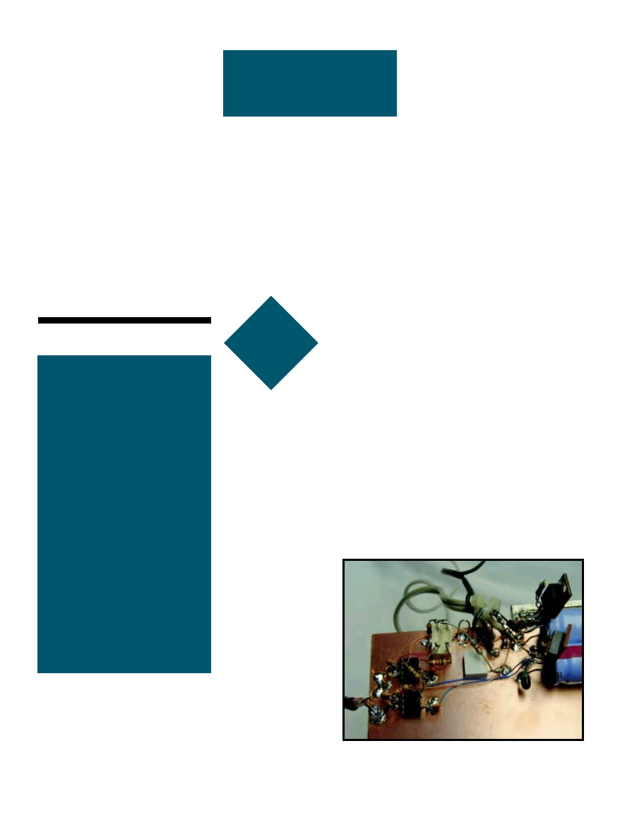
66
Issue 127 February 2001
CIRCUIT CELLAR
®
www.circuitcellar.com
l
et’s begin with a
survey. Everyone
who uses X10 power
line control gizmos put
your hand in the air. Now, lower your
hand if you’ve never experienced any
X10 poltergeists: lights blinking at odd
hours, modules that stop working for a
day, dead modules that start working
as soon as you think about replacing
them, a single outlet in a branch circuit
where X10 modules just don’t work,
and so on. Lots of hands waving in the
breeze out there. I thought this would
be an interesting topic!
Steve Ciarcia asked me to write a
column about “analog
and RF stuff.” What
better way to begin than
by looking at X10 com-
munications from the
analog side? Along the
way, I’ll examine an
active analog filter and a
construction technique
that makes analog
prototyping fast, func-
tional, and fun. Let’s
start by reviewing how
X10 is supposed to work.
THE DIGITAL SIDE
As you’ve read in
many Circuit Cellar
articles over the years,
X10 messages are sequences of 120-
kHz bursts sent through the 120-VAC
house power wiring. Although the
transmitter can drive up to about 5 V
onto the wiring at 120 kHz, an accept-
able signal at the receivers may be only
a few tens of millivolts.
An X10 message consists of a unique
two-cycle start code, a four-bit house
code, as well as a five-bit code that can
represent either a unit number or a
function code. The complete message
is 11 bits long, with each bit sent in
one 60-Hz power line cycle, and re-
quires 11 cycles.
Note that the raw data rate is
60 bits per second (or, if you’re in a
part of the world with 50-Hz power,
50 bits per second). The usable, or
payload, data rate is about 2/3 of the
raw rate, because each message re-
quires three “silent cycles” to give the
receivers time to process it. Obviously,
this is not the physical layer from
which house data networks arise.
Three 1-ms bursts that are synchro-
nized with a zero crossing of the AC
power line voltage represent each bit.
Photo 2 shows an All Lights On mes-
sage for house code P. With the excep-
tion of the start code, the three bursts
for each bit occur in the first half-cycle
for one bits and in the second half-
cycle for zero bits. The start code is
always nine bursts in three half-cycles,
followed by one half-cycle of silence.
Although each bit becomes three
bursts, X10 receivers detect only the
presence or absence of the first burst
To kick off his new
bimonthly column, Ed
decided to start with a
topic that would be of
interest to a lot of
readers. So, has any-
one ever experienced
quirks in their X10
system? Buckle up
and follow along as
Ed takes us above
the ground plane.
Bring the Noise!
ABOVE THE
GROUND PLANE
Ed Nisley
Photo 1—
The solid, gleaming, ground plane beneath the components in
this 120-kHz bandpass filter prototype helps reduce analog noise.
Mounting the op-amps upside down in dead bug style minimizes wire
length and reduces stray capacitance to ground.
The Analog Side of X10
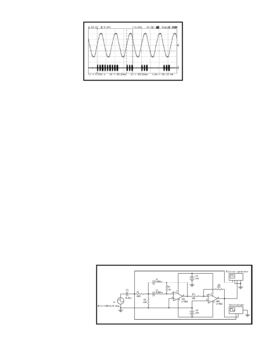
CIRCUIT CELLAR
®
Issue 127 February 2001
67
www.circuitcellar.com
after the zero crossing occurring
at the receiver. In a three-phase
power system, the transmitter
must send three bursts to ensure
that a burst occurs at the zero
crossing time of each phase, but
any given receiver can monitor
only its own phase, which may
lead or lag the transmitter. As a
result, X10 receivers cannot use
majority voting for error detec-
tion and correction.
There are some variations on
this format, but for the purpose
of this article, it’s enough to know that
there are neither parity bits nor error-
correction coding. X10 receivers can
reject messages when they detect an
incorrectly formatted data bit, but it’s
easy for noise to create bad messages.
But, why would there be any errors?
Photo 1 is unambiguous, isn’t it?
SEPARATING SIGNALS
In order to examine X10 signals
more closely, you must separate them
from the normal AC power line volt-
age found on the house wiring. You
want a circuit that will block 60-Hz
energy and transmit 120-kHz energy.
In the analog domain, that’s what fil-
ters do for a living, display a different
output behavior for input signals of
different frequencies.
Because the signals you’re interested
in differ greatly in frequency, a simple
filter will suffice. If the signals were
much closer together, the filter design
would become more complex. Let’s
start with a simple project and save the
tough stuff for later.
X10 modules use an inductance-
capacitance (known better by the ini-
tials of its electrical components, LC)
filter to isolate their control signals.
That filter, although adequate for the
task, was designed for a circuit built
inside an insulated plastic box, not one
exposed on a workbench.
Although X10 signal voltages are
harmless by themselves, inadvertent
contact with 120 VAC can be fatal.
Even though I enjoy writing this col-
umn, it’s not a job to die for! So, I used
a 24-VAC transformer to reduce the
line voltage to a manageable level at
the filter input and eliminate risk of
electrical shock. However, wall warts
designed for 60-Hz operation attenuate
120-kHz X10 signals. The wart from
my parts pile has an effective voltage
ratio of 4.2 at 60 Hz and 29.7 at
120 kHz, which means a 5-V X10 sig-
nal drops to 170 mV.
Obviously that means the filter
must not only separate X10 signals
from the power line voltage, but am-
plify them as well. The circuit shown
in Figure 1 does just that.
AR1 and the surrounding compo-
nents are an active bandpass filter,
with a 20-kHz bandwidth centered at
120 kHz. AR2 is a simple inverting
amplifier that boosts the filter’s volt-
age output by a factor of about five.
C3, at the input of AR1, acts as a high-
pass filter that reduces 60-Hz signals
by a factor of about 300.
Maybe that’s easy for me to say.
You may ask, “How do I get from
knowing what I want to do, to actually
having a working analog circuit?”
Good question! That’s what this
column is all about, getting from here
to there. You must venture far from
the digital domain to (cue dramatic
music) soar above the ground plane.
LIGHTING THE TORCH
After you’ve decided the rough
shape of the circuit you want (in
this case, a bandpass active filter
with a bit of amplification), the
next step is to consult the books.
You know what I’m talking about,
those books on your electronics
bookshelf. If you don’t have any
books, you’re doomed.
You can’t invent this stuff from
scratch for every situation you’ll
encounter. Take advantage of
engineers who have already fig-
ured things out, worked out the intri-
cacies, and tabulated the results.
The first book you must get is The
Art of Electronics
. This is one of the
few 1000-page technical books that
isn’t filled with fluff; every page has at
least one “I didn’t know that!” revela-
tion. It covers the basics of analog
circuitry, then explores low-level, low-
noise, high-frequency, RF, digital, dis-
crete, LSI, and, yes, even software
design. Just get it.
Next, you’ll need The ARRL Hand-
book for Radio Amateurs
. Not just for
hams, it contains a wealth of analog
design and construction techniques
that will make your life a lot easier, no
matter what you’re building.
While you’re at it, you should also
get a ham radio license. Anybody read-
ing this can probably pass the exam
cold, but I recommend looking up your
local ham radio club, signing up for a
license course, and discovering who
else in the area shares your interests.
Even if you have no desire to talk to
somebody in Tierra del Fuego, a ham
radio license permits you to experi-
ment with RF projects legally. The
Figure 1—
The first op-amp is a bandpass filter centered on the 120-kHz X10 signal frequency. Because the
wall wart transformer strongly attenuates X10 signals, the second op-amp boosts the filter output. Capacitor
C3 reduces the 60-Hz power line amplitude at the input to the filter while contributing significant phase shift.
Photo 2—
A pristine X10 signal from a nearby transmitter is shown
here. The sinewave comes from a transformer that isolates the
circuit from the power line. The filter enhances the X10 bursts.
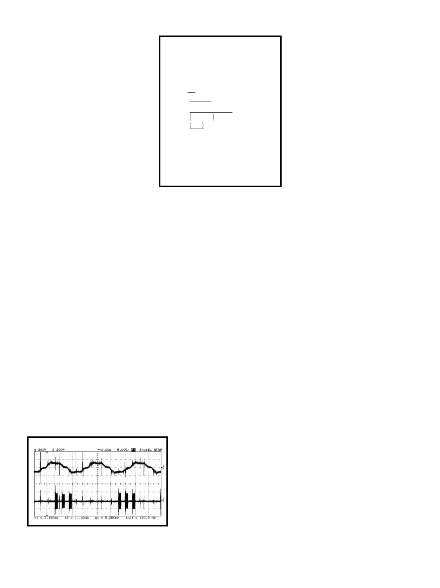
68
Issue 127 February 2001
CIRCUIT CELLAR
®
www.circuitcellar.com
ticket doesn’t require learning Morse
code and gives you access to ham
bands from 50 MHz on up.
The ARRL also publishes a variety
of special-interest books that may be
handy. Interested in spread-spectrum
wireless? The ARRL has the knowl-
edge! I’ll discuss some RF projects in
future colums, so if you’re not licensed,
you’ll miss some fun. Again, just get it.
Finally, semiconductor makers put
considerable time and effort into pro-
ducing their application notes. It’s
amazing that many engineers never
read them, because app notes are some-
times the only way to find out how to
design the circuit surrounding an IC.
Nowadays, all the app notes you
need are online. Given a dial-up ISP
account, I find it easier to download
the PDF documents (or order a CD-
ROM catalog), but your mileage may
vary. Set up Adobe’s Acrobat Reader,
then start trolling the ’Net.
FILTERING FUNDAMENTALS
The filter topology in Figure 1
comes straight from the ARRL hand-
book’s chapter on filters. I tapped the
design equations into the Mathcad
worksheet shown in Figure 2, plugged
in the desired performance, and it spat
out the resistor values. However, if
you compare the Mathcad results with
the resistors in Figure 1, you’ll see that
they don’t match. What gives?
In the digital domain, you can be
reasonably sure that a one is a one, a
zero is a zero, and what your design
equations predict is what will happen.
That’s true at least until your clock
hits the tens of megahertz, when you
discover that high-speed digital design
and layout require analog skills.
Here above the ground plane, in the
analog domain, you can be reasonably
sure that things are not as they appear
in the equations. Those equations in
Figure 2 assume you’ll build the circuit
from exact resistors, perfectly matched
capacitors, and ideal op-amps. The real
world is rarely so accommodating.
So, the next step in analog design
(for any nontrivial circuit) is dumping
the circuit into a simulator and seeing
what happens. I use an old version of
Electronics Workbench, but there may
be better SPICE simulators out there.
One thing that’s an eye-opener is
changing the type of op-amp in the
circuit. Start with an ideal op-amp, try
a good old 741, an LF441, then some-
thing with a better gain-bandwidth
product like the LF356 I used. Then go
read about why op-amps aren’t ideal in
The Art of Electronics
.
For this noncritical circuit, I used
5% carbon-film resistors, hand-
matched Mylar caps, and LF356
op-amps. The resistor values I
settled on (after iteration) produce
simulated center frequency and Q
values close to the desired values
shown in Figure 2.
Simulation is not the real
world. After you simulate the
circuit, you must build it and
measure its behavior to verify
that you didn’t leave something
out. I performed the verification,
and it’s pretty close.
But, how do you build an analog
circuit?
LET’S GET UGLY
First of all, those solderless bread-
boards you probably use are not a good
idea for analog circuitry. They have
high parasitic capacitance among pins,
lousy power distribution, and terrible
reliability. They’re OK for teensy digi-
tal projects, but leave them on the
shelf for anything you care about.
Photo 1 shows what Figure 1 looks
like in real life. The first thing you’ll
notice is parts sticking out all over.
Compared to a neat printed circuit
board, it’s, well, it’s ugly. Which is
precisely what this method of
prototyping is called—ugly construc-
tion. Another name, dead bug con-
struction, refers to the way DIP ICs get
mounted upside down with their legs
in the air. If you must impress your
boss, call it ground-plane construction.
Despite the informal look, ugly
construction actually is a good way to
build analog circuits that operate
through the high HF and low VHF
frequencies. Beyond about 50 MHz, the
size of the circuit elements and para-
sitic capacitances to ground start af-
fecting the circuit response. But, that
doesn’t eliminate many of the projects
you were thinking of, does it?
Off on the right of Photo 1 is the
±15-V power supply that doesn’t ap-
pear in the schematic. For the low
currents involved here, I used a pair of
half-wave supplies with LM317 and
LM337 regulators.
I did, however, use separate wall
warts for the DC supplies and AC sig-
nal, mostly because that let me use a
higher voltage for the signal trans-
former. You may use a single wart, as
long as you remember that both warts
must be AC-output units, without
built-in rectifiers and filters!
Although the directions for ground-
plane construction tell you to make
secure mechanical connections be-
tween components before applying
solder, no one does. For prototypes
like this, a secure solder joint is suffi-
cient; if you make bad joints, you’ll
smarten up in a hurry when they fall
apart. Although I don’t advocate struc-
tural solder, if the component leads
Photo 3—
Noise is more evident from this remote X10
transmitter. The sinewave comes from the right side of C3
and shows a 90° phase shift. Note the changed oscilloscope
scales.
Butterworth bandpass filter
Inputs:
f
c
= 120 × kHz Center frequency
K = 10 Gain
BW = 20 × kHz Bandwidth
C = 1 × nF C1 and C2
Equations:
ω
0
= 2
× π ×
f
c
Q =
f
c
BW
R1 =
Q
K
× ω
0
×
C
R2 =
Q
2
×
Q
2
– K
× ω
0
×
C
R3 =
2
×
Q
ω
0
×
C
Angular frequency
Quality factor
Results:
Q = 6.0
R1 = 795.775 × 10
0
Ω
R2 = 128.351 × 10
0
Ω
R3 = 15.915 × 10
0
Ω
Figure 2—
Take a look at the Mathcad worksheet
with design equations for the X10 bandpass filter.
Note that the resistor values do not match what
you see in Figure 1.
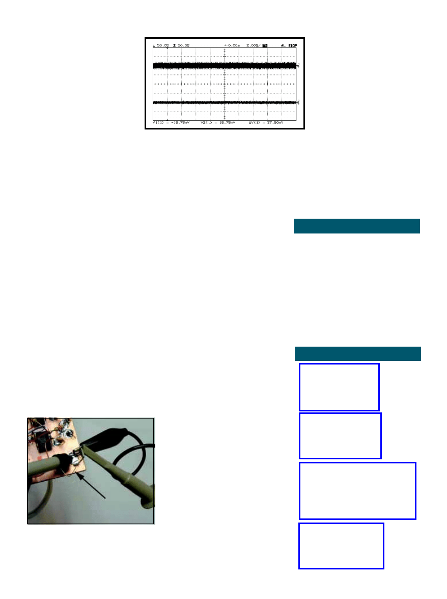
70
Issue 127 February 2001
CIRCUIT CELLAR
®
www.circuitcellar.com
SOURCES
SOURCES
Acrobat Reader
Adobe Systems Inc.
(408) 536-6000
Fax: (408) 537-6000
www.adobe.com
Mathcad
MathSoft, Inc.
(617) 577-1017
Fax: (617) 577-8829
www.mathsoft.com
X10 Modules
X10, Ltd.
(852) 2334-6848
Fax: (852) 2764-2437
www.x10.com
SOURCES
RESOURCES
K. Davidson, “The X-10 PL513
Power Line Interface Module,”
Circuit Cellar
3, 1988.
P. Horowitz and W. Hill, The Art of
Electronics
, 2d ed., Cambridge
University Press, Cambridge, U.K.,
n.d.
American Radio Relay League, Inc.,
The ARRL Handbook for Radio
Amateurs 2000
, American Radio
Relay League, Inc., Newington,
CT, November 1999.
Ed Nisley is an electrical engineer. In
addition, he is a ham radio hobbyist
(call sign KE4ZNU). You may reach
him at ed.nisley@ieee.org.
firmly contact each other and
aren’t under tension when you
apply solder, things will work fine.
I don’t recommend ugly con-
struction for circuitry that’s going
into active service though. If you
plan to make more than one of
them or if the gizmo is more than a
bench prototype, you should plan
on a printed circuit version. But,
for the first prototype or two,
remember, ugly rules!
Whenever a component con-
nects to ground, simply solder it to
the copper sheet. You can use high-
value resistors as standoffs. Unless
you’re working with high-impedance
circuitry, a 1-M
Ω
resistor is effectively
an open element that conveniently
holds a circuit node off the plane.
When you work with surface-mount
circuitry, you’ll look back on ugly
construction with fond memories.
MIND THE LOOP!
Photo 3 shows X10 bursts from a
transmitter on a different branch cir-
cuit than my workbench. The scope
voltage scales are 10 times more sensi-
tive and there’s more crud on the sig-
nals. Most impulse noise is synch-
ronized with the AC signal. Power
supplies and dimmable lamps contrib-
ute that sort of noise to the line; any
time you fire a triac or switch a diode,
a blast of noise enters the power line.
As the analog signals you’re inter-
ested in become smaller, the noise
becomes larger. And, measurement
techniques that you use for digital
circuitry will turn around to bite you.
As a simple example, both traces in
Photo 4 show ground potential at a
scale of 50 mV per division, but the
top trace is thicker. If you have such a
great ground plane (and you do), why is
it so noisy?
In order to understand the problem,
you must think in terms of current, not
voltage. The ground clip and long wire
on your favorite scope probe form a
loop. The wire and sheath of the probe,
right down to the tip, are a one-turn
coil. A varying magnetic field passing
through that loop will induce a voltage
across the scope’s input circuitry. And
it doesn’t take much current either.
The effective impedance at the
scope probe tip is 10 M
Ω
. The cursors
in Photo 4 indicate about 38 mV of
noise peak-to-peak, which means the
effective current is 3.8 nA
p-p
. I’ll let you
work out the conversion to your favor-
ite magnetic unit, but it’s small stuff.
In order to succeed in the analog
domain, you must change your habits.
Find the little bag of parts that came
with your scope probe, find the tip
with a ground wire coming out of the
side, and throw away the alligator clip.
In Photo 5, the arrow marks the ground
connection that produced the bottom
trace in Photo 4.
CONTACT RELEASE
I planned to show you a bestiary of
hideous X10 noise problems, but, after
I built this circuit and began monitor-
ing my power line, every one of my
X10 poltergeists vanished! All the
modules began working perfectly and
none of the lights blink in the middle
of the night. Life is good.
And that’s true even with the filter
unplugged and the scope turned off.
Talk about a successful project! I
will report back to you when the
poltergeists return, as they cer-
tainly will.
Until next time, gather an
assortment of circuit boards that
have not been etched, a handful of
parts, and get ugly. See what your
power line looks like through an
X10 bandpass filter, get some
experience measuring analog sig-
nals, and learn a few new tricks. It
can’t hurt, unless you forget the
isolating transformer!
I
Photo 4—
Measuring just the ground plane potential reveals a
common analog mistake. The only difference between the two
channels is the length of the connection to the plane.
Photo 5—
In the analog world, connections are not
always what they seem. The probe on the right
sports the usual alligator ground clip. The short
ground wire on the left probe, marked by the arrow,
produces the bottom trace in Photo 4. ’Nuff said?
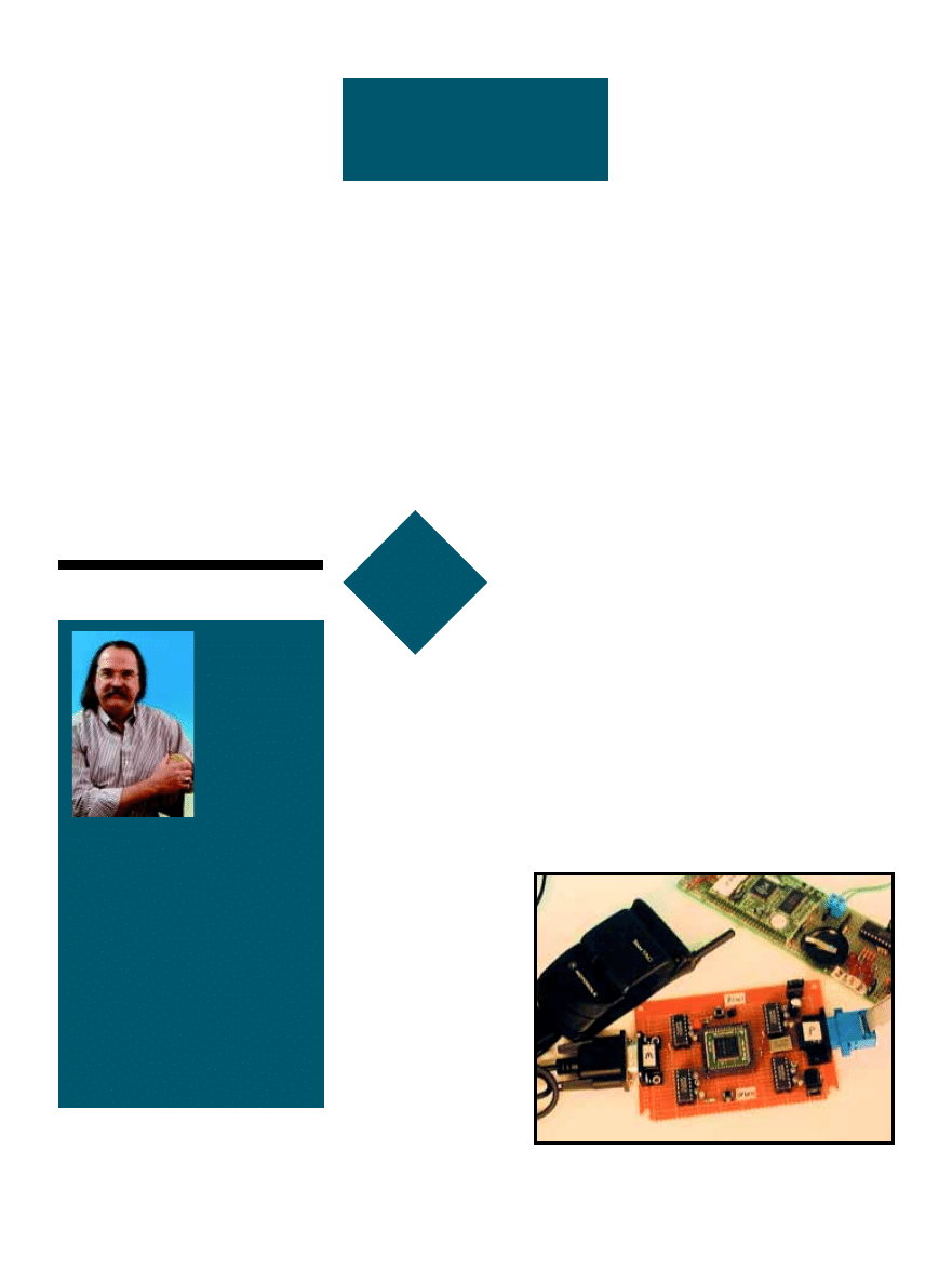
72
Issue 127 February 2001
CIRCUIT CELLAR
®
www.circuitcellar.com
FROM THE
BENCH
Jeff Bachiochi
Car 54, Where (Exactly)
Are You?
Adding E-Mail Capabilities to Your
Project
Last
month,
Jeff’s
project
was a
practical GPS appli-
cation for tracking a
vehicle. This month
he adds the power
of e-mail to make his
Autolocater even
more effective.
hat do you
mean you like
having your stolen
car report its position
directly to you, but don’t want to
dedicate a computer and phone line to
the task of waiting for your car to be
stolen? OK, so maybe your computer
doesn’t have to be dedicated because
your phone line is tied up by teenagers
for hours on end. Last month’s GPS
Autolocator project has just one short-
coming. If you aren’t around to re-
ceive its call, you’ll miss your chance
to quickly find your ve-
hicle. This month, I apply
one more link in the
chain to make this system
work whether you’re
home or not.
What you need is a
way to store messages so
they can be read at any
time from wherever you
wish. Sounds like e-mail,
doesn’t it? What does it
take to send an e-mail
message? In terms of
hardware it requires a
host processor with gobs
of memory to support all
the protocols. You’ve
w
probably seen Figure 1 before; it
shows the stack of protocols necessary
for dial-up Internet communications.
This wall of protocols begins with
your application running at the top and
ends with the physical hardware pro-
viding the transfer at the bottom. In
between are protocol layers that
handle various tasks depending on the
actual job. For this project, you need to
use the SMTP (simple mail transfer
protocol, RFC821) from the applica-
tions layer to handle the basic to/from/
text information. Next, the TCP (trans-
fer control protocol, RFC793) from the
transport layer “packetizes” the data.
Then the IP (Internet protocol,
RFC791) from the network layer wraps
up the packets for routing over the
Internet. Finally, the PPP (point-to-
point protocol, RFC1661) from the
link layer handles the actual hardware
interfacing (in this case, a modem).
With sufficient ROM and RAM, you
could study all of the protocols and
write an application to handle this,
but if you’re like me, you want an
easier way. Don’t get me wrong, I
enjoy the nitty-gritty but this is more
than a quick fix. How many of you
use your own hand-written protocol
for sending a file to another person?
You probably use established FTP
protocols and the AT command set
when dealing with a modem. Hayes
invented the AT command set for its
Smartmodem back in 1981. This de
facto standard is still used today by
every modem manufacturer. Hayes
implemented high-level functions
Photo 1—
Positioned between the processor and the modem (cell phone),
this circuitry allows a micro to do Internet-related tasks without the re-
sources normally associated with TCP/IP.
CIRCUIT CELLAR
®
Issue 127 February 2001
73
www.circuitcellar.com
Parameter
Type
Range
Default
Description
LVS
Byte
0…1
1 (yes)
Leave on server: 1 (yes), 0 (no).
HDL
Byte
0…255
0 (no limit)
Limit number of header lines retrieved.
XFH
Byte
0...1
1
Transfer e-mail headers. 1 (Enable), 0 (Disable).
FLS
String
62 chars
NULL (no filter)
Filter string must exist in message header to qualify for retrieve.
SBJ
String
96 chars
NULL
Contents of the e-mail subject field.
TOA
String
32 chars
NULL
Primary addressee, to where e-mail will be sent.
TO
String
96 chars
NULL
Addressee description/name in e-mail header.
REA
String
32 chars
NULL
Return e-mail address.
F R M
String
96 chars
NULL
Sender description/name in e-mail header.
CCn
String
32 chars
NULL
Alternate addressee (CC: field) <n>:1..4.
ISPn
Phone #
32 chars
NULL
ISP’s access phone number. <n>:1..2.
ATH
Byte
0…2
1 (PAP)
Use CHAP(2), PAP(1), or Script(0) authentication.
USRN
String
32 chars
NULL
ISP connection user name.
PWD
String
32 chars
NULL
ISP connection password.
DNSn
IP
address
0.0.0.0
Domain name server IP address: <n>:1..2.
SMTP
String
32 chars
NULL
SMTP server name.
POP3
String
32 chars
NULL
POP3 server name.
MBX
String
32 chars
NULL
Mailbox user name.
MPWD
String
32 chars
NULL
Mailbox password.
RDL
Byte
0…20
5
Number of redial tries.
RTO
Byte
0…255
180
Timeout before redialing.
BDR
Byte
1…8
‘a’ (auto data rate)
Sets the iChip to auto data mode.
*Retained for backwards compatibility.
BDRF
Byte
…8
‘a’ (auto)
Sets the iChip! host to a fixed data rate.
BDRM
Byte
1…8
‘a’ (auto)
Sets the iChip! modem data rate to a fixed rate.
FLW
Byte
0…1
0 (S/W)
Flow control mode.
XRC
Byte
0…4
4
Extended return code; same as ATXn.
MIS
String
126 chars
AT&FE0V1X4Q0...
Modem initialization string.
MT
Byte
0…4
4
(Application) Media type: 0-Text; 1-Image; 2-Audio; 3-Video; 4-
Application
MST
String
octet-stream
Media subtype string. For a list see appendix A.
BDY
Text
lines
NULL
Textual body contents for MIME encapsulated e-mail messages.
F N
String
None
Attachment file name (inc. extension). If a file name is not
defined, the iChip will generate a unique file name.
URL
String
128 chars
None
URL string used for subsequent +iRLNK and +iSLNK commands
to download/upload web pages and files.
that handled things like going off
hook and establishing a modem link
by simply using the ATDT# com-
mand. Feedback is returned through
simple text as well (e.g., “CONNECT
9600”). You ultimately need AT com-
mands that are Internet-related.
In Alan Singer’s article, “Internet
Connectivity” (Circuit Cellar 123), he
discussed the pros and cons of design-
ing an interface from scratch instead
of using an off-the-shelf solution. He
used Connect One’s iChip, which
comes in two varieties, a serial/paral-
lel and a LAN interface. When de-
signed in as a system peripheral, the
iChip handles an Ethernet LAN con-
nection or a dial-up or wireless mo-
dem. The fact that it contains flash
memory, CPU, and RAM plus local
and host interfaces is a wonder. But
that isn’t what makes this special.
Connect One added AT commands to
handle Internet dealings. Like AT
modems, the iChip has nonvolatile
memory that you can load with all the
pertinent data (see Table 1).
As the table explains, these are the
basic pieces of information needed for
any kind of transfer. Storing this data
simplifies the amount needed when
issuing one of the included com-
mands. This data and the iChips’s
command set are accessible using the
+I extensions to the AT command set.
The AT+I command precedes all of
Connect One’s inter/intra/extranet
commands. Because the iChip periph-
eral is positioned between the host
and modem (or LAN), commands that
don’t include the +I extension are
passed through the iChip to any con-
nected modem. In this way, the iChip
won’t affect AT commands meant for
the modem. But, commands that con-
tain the +I extension are eaten by the
iChip, and the appropriate commands
are issued to the modem to handle all
of the tough stuff. The iChip can
handle most protocols.
Take a look at the
AT+I command set in
Table 2. Notice the
last command. The
iChip firmware re-
sides in flash memory
so it can be updated
dynamically from
either the host or
through the Internet
connection. This
allows the iChip to
stay current if the
protocols change.
Last month, I used
my cell phone to
make contact with
my computer without
an ISP. The wireless
connection was used
to pass the current
time/date/location to
my computer, which
was acting as a host.
Although complete, it
requires the computer
to be on and available
to receive the call. By
inserting the iChip
between the micro,
(which has collected
time/date/location
information from a
GPS connected to it)
and using the cell
Table 1—
These nonvolatile parameters are used for defaults when not explicitly used in an immediate command. These parameters are
similar to the
init
string stored for most modems.
Photo 2—
The iChip is a compact 68-pin PLCC
multichip carrier. The iChip is one compact circuit, soon
to become an ASIC.

CIRCUIT CELLAR
®
Issue 127 February 2001
75
www.circuitcellar.com
Command
Function
Parameters/description
AT+i
Commands prefix
Required to precede all commands.
Host interface
E n
Echo mode
n = 0—Do not echo host characters.
n = 1—Echo all host characters.
This command is equivalent to and interchangeable with ATEn.
Parameter database maintenance
<par>=
value
Sets parameter
value stored in parameter <par> in nonvolatile memory. <par> will retain set value across power
or
down, indefinitely. For description of all available parameters see section 4.3.
<par>:
value
<par>~
value
Assigns single
session
value is assigned to parameter <par> for the duration of a single Internet session.
Following the parameter value session the original value is restored.
<par>?
Read parameter
Parameter value is returned.
<par>=?
Parameter what?
Returns the allowed values for this parameter.
FD
Factory defaults
Restores all parameters to factory defaults.
Status report
RP<i>
Requests report status Returns a status report value or sets a status report mode based on <i>.
E-mail send immediate
[!]EMA:<text>
Sends textual e-mail
Defines the textual contents of the e-mail body. Following this command
immediate
several text lines may be sent in sequence. Sending a CR.CR (line containing only a period)
terminates the text body. After termination, the e-mail is sent automatically. Total <text> size is
limited to 18 KB.
[!]EMB
:
<sz>,<data>
Send binary e-mail
Prefixes a binary datastream. The data is encapsulated as a base64 encoded MIME attachment.
Following this prefix, exactly <sz> bytes are streamed to the iChip. For values of <sz> greater than
256, iChip/iModem’s software flow control applies.
[!]E*
Terminates binary
Terminates a binary (MIME attachment) e-mail.
Retrieve e-mail from mailbox
[!]RML
Retrieves mail list
Retrieves an indexed, short form list of all qualifying messages in mailbox.
[!]RMH[:<i>]
Retrieves header
Retrieves only the e-mail header part from the <i>’th e-mail in the mailbox or the entire mailbox.
[!]RMM[:<i>]
Retrieves e-mail
Retrieves all e-mail contents of the <i>’th e-mail in the mailbox or the entire mailbox.
HTTP client download
[!]RLNK[:<URL>]
Retrieves link
RetrievesC a file from a URL on a web server. If <URL> is not specified, use the URL stored in the
URL parameter.
Socket interface
STCP:<host>,<port>
Socket TCP
Opens and connects a TCP socket. If the iChip is not online, the ISP will be connected.
The responding system is assumed to be a server “listening” on the
specified socket. Responds with a handle to the socket.
SUDP:<host>,<port>
Socket UDP
Opens and connects a UDP socket. If the iChip is not online, the ISP will be
connected. Responds with a handle to the socket.
SSND[%]:
<hn>,<sz>:<stream>
Socket send
Sends a bytestream of size <sz> to the socket identified by handle <hn>. ‘%’
flags autoflush socket.
SRCV:<hn>[,<max>]
Socket receive
Receives a bytestream from the socket identified by handle <hn>. Accept maximum <max>
bytes. If <max> is not specified, all available bytes are retrieved.
SDMP:<hn>
Socket dump
Dumps all buffered inbound data that has arrived in the socket identified by handle <hn>.
SFSH:<hn>
Socket flush
Flushes all buffered outbound data, sent to the socket identified by handle <hn>.
[!]SCLS:<hn>
Socket close
Closes the socket identified by handle <hn>.
Connection
BDRA
Auto baud mode
Forces the iChip into auto baud rate detection mode.
DOWN
Disconnect from
This command forces the iChip to terminate an Internet session and go offline.
Internet
Remote firmware update
F U
Firmware update
In a modem configuration, enters firmware update mode.
Table 2—
These commands are Connect One’s +I command extensions to the now standard AT command set. The extension commands allow you to ask the iChip
to perform Internet-related tasks, just as the AT command set controls modem functions.
phone as a wireless modem, I can send
an e-mail message to my ISP and re-
ceive that e-mail from anywhere.
TWO SERIAL PORTS
I’m using the iChip’s serial mode
to modify last month’s project and
make it a no-brainer. Looking at Figure
2, you can see the minimum circuitry
necessary to take advantage of the
iChip power. Most of the circuitry is
level shifters to interface with RS-232
signals (see Photo 1). Note that by
designing the iChip into the original
circuitry, you can eliminate the level
shifters. But, as a separate unit this
can easily be added to any existing
project, giving it Internet capability.
Code for this project is simplified
(assuming the nonvolatile registers are
pre-loaded with the necessary data).
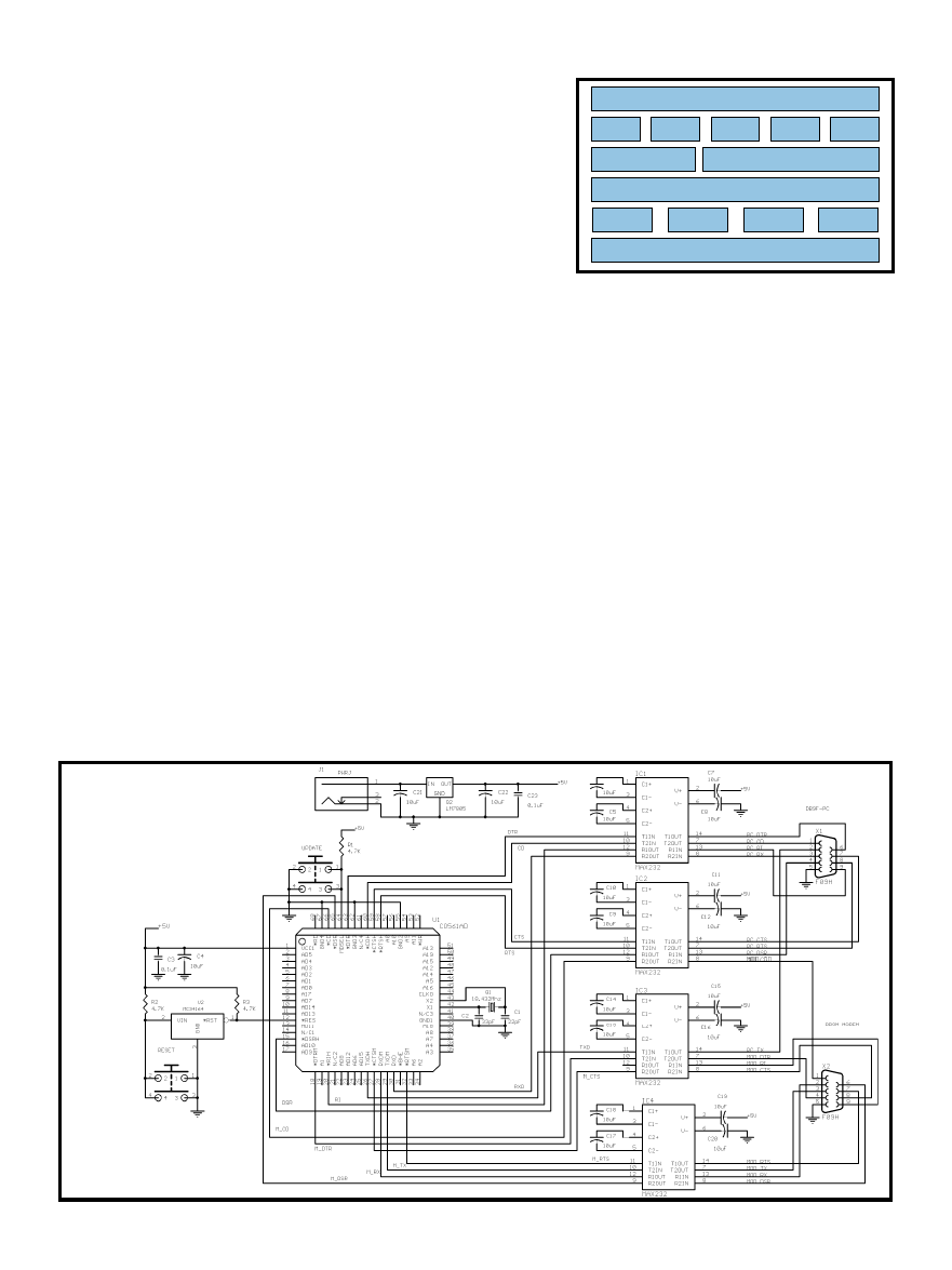
76
Issue 127 February 2001
CIRCUIT CELLAR
®
www.circuitcellar.com
My last article, “Where’s Waldo?”
(Circuit Cellar 126), employed the
following steps:
•
lower DTR TTL output (enable
StarTAC modem)
•
use ATDT command to dial modem
•
look for reply connection
•
send data
•
raise DTR TTL output (disable
StarTAC modem)
Take a look at this month’s steps:
•
lower DTR TTL output (enable
StarTAC modem)
•
use AT+IEMA: command to send e-
mail to ISP using SMTP
•
look for reply I/OK
•
look for reply I/DONE
•
raise DTR TTL output (disable
StarTAC modem)
Actually, the parameter data can
easily be included in your application,
giving you complete control (i.e., e-
mail Subject Field or e-mail Circuit
Cellar
address from Table 1). Each
parameter can be written to the iChip
as data to be saved to NV storage or
used as one-time data by appending an
approximation. For an example of
this, you should take a look at
<par>~value in Table 2.
HOW’D IT DO THAT?
When I issue the AT+IEMA:
command followed by the mes-
sage text closed with <cr>
<lf>.<cr><lf>, the iChip re-
sponds with I/OK. This re-
sponse indicates that it has all
the information it needs to
handle the rest of the e-mail
function. Using the parameters
in NV storage (or the immedi-
ate data when using ~), the
iChip establishes a connection
with your ISP by sending AT
commands to the modem. It
logs on by authenticating your user
name and password and then enters
the SMTP mail server by authenticat-
ing your mailbox username and mail-
box password. Then, the e-mail data
transfers and the mail server is sus-
pended. The ISP connection is broken
and the iChip responds with I/DONE.
This message lets you know that all
went well; other resultant codes are
possible depending on the outcome of
the operation (see Table 3).
TECH SPECS
The iChip provides for data rates
up to 57,600 bps (230,000 bps with
LAN-supported device) in an 8-N-1
data format. The firmware can be
updated directly through the modem
connect with a direct connection (PC
modem to iChip modem) or through a
phone line (PC modem to phone to
iChip modem). The firmware transfer
is done via the Y-MODEM protocol.
In a successful download, the iChip
transfers the new code into its flash
memory and reinitializes.
The iChip always interfaces to the
host processor through a full-duplex,
TTL-level serial communications
link. Full EIA-232-D hardware flow
control, including Tx, Rx, CTS, RTS,
and DTR lines, is supported. The host
processor can program the iChip to
use hardware flow control or wait/
continue software flow control be-
tween the iChip and the host CPU.
The flow control mechanism is based
Figure 2—
I used the iChip
in its simplest form, serial-
in, serial-out. MAX232-level
shifters are necessary only
when connecting via EIA-
232-D supported devices.
Application-specific protocols
DNS
TIME
SMTP
POP3
HTTP
UDP
TCP
IP
LCP
PPP
IPCP
PAP/CHAP/
SCRIPTS
Communications platform
Figure 1—
The dial-up Internet protocol stack is shown here as the
protocol layers necessary between your application and the
physical hardware. Every protocol in every layer has an Internet
standard associated with it. These protocol standards can be found
on the ’Net by searching for RFC.
78
Issue 127 February 2001
CIRCUIT CELLAR
®
www.circuitcellar.com
Jeff Bachiochi (pronounced BAH-key-
AH-key) is an electrical engineer on
Circuit Cellar’s engineering staff. His
background includes product design
and manufacturing. He may be reached
at jeff.bachiochi@circuitcellar.com.
SOURCE
on the RTS/CTS signals. Flow control
between the iChip and modem can be
individually programmed to hardware
flow control or no-flow control.
Connection to a dial-up modem
may be a full-duplex, TTL-level serial
(featuring EIA-232-D hardware flow
control including Tx, Rx, CTS, RTS,
and DTR) or an 8- or 16-bit parallel
configuration (using CE, read, write,
IRQ, and address).
The LAN iChip directly supports a
CS8900 IEEE 802.3 Ethernet controller
in 16-bit memory mode. Interrupt and
DMA requests are directly connected
to dedicated inputs. A small PLD or
discrete logic is required to generate
MEMRD#/MEMWE# and IORD#/
IOWR# signals from the iChip’s RD#
and WR# signals to simulate memory,
I/O, and DMA accesses.
Today, the iChip is a 68-pin PLCC
multi-chip carrier containing proces-
sor, RAM, and flash memory (see
Photo 2). Both 5.0- and 3.3-V versions
of the iChip are available. A power-
saving mode reduces the current from
160 mA (typical) to 10 mA.
DEVELOPMENT TOOLS
Connect One makes it easy to evalu-
ate the iChip. It offers a complete line
of evaluation units. The documenta-
tion comes on a CD and covers the
iChip, iModem, iChip software, and
AT+I command set. This support
made my task easier to accomplish. I
will use the iChip in future designs. It
has allowed this project to achieve a
state of merit without compromise.
WARNING
It’s easy to get carried away with
possibilities for a project that can be
used for tracking. I grew up worrying
about the potential for nuclear war
and Big Brother watching, and I’m not
looking to promote such a concept.
Each of us has different levels of para-
noia when it comes to our right to
personal privacy. Although we must
never relinquish those rights, there
are times when knowing where you
are can be used in positive and pro-
ductive situations. Let’s make sure
these areas are explored without deny-
ing us our constitutional rights.
I
Resultant text
Code
Description
I/OK
30
Command was successfully executed.
I/BUSY
31
iChip B = busy. Command discarded.
I/DONE
32
iChip completed Internet activity. Returned to command mode.
I/ONLINE
33
iChip completed an Internet activity but has remained online as a result of
the stay-online flag (!).
I/RCV
34
Marks beginning of e-mail Retrieve mode with XFH=1. iChip will not
respond to any commands, excluding “+++” (Break).
I/PART
35
Marks beginning of MIME attachment part.
I/EOP
36
Marks end of MIME attachment part.
I/EOM
37
Marks end of e-mail message during retrieve.
I/MBE
38
This flag is returned when attempting to retrieve mail from an
empty mailbox.
I/ERROR (nnn)
nnn
Command error encountered. Command discarded.
Code
Description
Code
Description
41
Illegal delimiter
100
Error restoring default parameters
42
Illegal value
101
No ISP access numbers defined
43
CR expected
102
No USRN defined
44
Number expected
103
No PWD entered
45
CR or “,” expected
104
No DNS defined
46
DNS expected
105
No POP3 defined
47
“:” or “~” expected
106
No MBX (mailbox) defined
48
String expected
107
No MPWD (mailbox password) defined
49
“:” or “=” expected
108
No TOA (addressee) defined
50
Text expected
109
No REA (return address) defined
51
Syntax error
110
No SMTP defined
52
“,” expected
111
Binary e-mail data overflow
53
Illegal command code
112
Command illegal when modem online
54
Error when setting
200
Socket does not exist
55
Parameter value error
201
Socket empty on receive
when getting parameter value
56
User abort
202
Socket not in use
57
Error when trying to establish PPP
203
Socket down
58
Error when trying to establish SMTP
204
No available sockets
59
Error when trying to establish POP3
205
Socket receive buffer full
60
Single session body
206
PPP open failed for socket
61
Internal memory failure
207
Error creating socket
62
User aborted the system
208
Socket send error
63–66
Reserved
209
Socket receive error
67
Command ignored as irrelevant
210
PPP down for socket
68
Reserved
211
TCP down for socket
69
Timeout on host communication
212
Socket flush error
70
Modem failed to respond
213
Internal error
71
No dial tone response
214
Internal error
72
No carrier modem response
215
Internal error
73
Dial failed
216
General exception
74
Connection with ISP lost
217
Out of memory
75
Access denied to ISP server
300
HTTP server unknown
76
Unable to locate POP3 server
301
HTTP server timeout
77
POP3 server timed out
302
HTTP failure
78
Access denied to POP3 server
303
No URL given
81
Unable to locate SMTP server
304
Bad HTTP host name
82
SMTP server timed out
305
Bad HTTP port number
83
SMTP failed
306
Bad URL address
84-99
Reserved
307
URL address too long
Table 3—
Similar to the Hayes AT command set, the iChip can give both text and code results from an
executed command. This information can be used to regroup and decide what to do next in case of an error.
80
Issue 127 February 2001
CIRCUIT CELLAR
®
www.circuitcellar.com
i
t’s the people’s
micro, marching
bravely into battle
with monopolistic mi-
cro robber barons and decadent RISC
revisionists….
Originally designed by Intel more
than 20 years ago, the ’51 has become
a public good, these days better serv-
ing the masses than its main-squeeze
PC chips.
Overall, the ’51 numbers are stag-
gering. From what I can figure out, the
’51 run rate is even more than one
million a day! Where are they all go-
ing? Who knows? They’re just poster
proletariat for the 8-bit micro masses
that labor day in and day out, taking
care of the mundane housekeeping
and dirty work disdained by upper-
class chips.
Intel, a company known for being
tightfisted with its intellectual prop-
erty, is responsible for the ’51, which
has essentially become free for the
taking as an open-source chip. There
were less lawyers hanging around way
back when and, in any case, time
would’ve run out on what few patents
were in place.
The result is that the ’51 is a
uniquely profligate architecture. Un-
like other 8-bit chips from heavy-
weights like Motorola, Microchip,
’51 Soldiers On
SILICON
UPDATE
Tom Cantrell
Over
time, the
’51 has
proven
itself to
be a valuable work-
horse micro that’s
shown up in the
stables of a variety of
manufacturers. With
such a successful his-
tory, it’s no wonder the
’51 is still growing.
Hitachi, and so forth, ’51 derivatives
are available from quite a few sources,
both big and small.
What this means is that there’s a
lot of ongoing innovation and super-
wide selection that easily exceeds
single-source architectures. Hardly a
month goes by before yet another
press release about some new and
improved ’51 finds its way into my in
basket to read.
Philips, probably the single largest
’51 supplier, follows up last year’s
introduction of its low pin-count (LPC)
parts with even more downsizing in
the form of a tiny TSSOP package that
measures barely a 1/4
″
per side.
Cygnal continues to flesh out its line
of flash memory analog ’51s with up
to 12-bit A/D resolution, even as
Analog Devices ups the ante with a
16-bit A/D version of its own flash
memory ’51.
DALLAS TECHS US
The winner of the ’51-of-the-month
award goes to Dallas Semiconductor
for its brand-new DS89C420.
I think Dallas deserves credit for a
contribution to the 8-bit market that
goes beyond its share of the business.
There was a time back in the ’80s
when the belief was widespread that 8-
bit micros would succumb to the
march of progress at the hands of
high(er)falutin 16-bit micros. Perfor-
mance was topping out at a few MIPS,
leaving a bunch of the anticipated and
potential markets on the table, and
none of the 8-bit suppliers seemed to
have much to say about it.
1
2
3
4
5
6
7
8
9
10
11
12
13
14
15
16
17
18
19
20
P1.0/T2
P1.1/T2EX
P1.2/RXD1
P1.3/TXD1
P1.4/INT2
P1.5/*INT3
P1.6/INT4
P1.7/*INT5
RST
P3.0/RXD0
P3.1/TXD0
P3.2/*INT0
P3.3/*INT1
P3.4/T0
P3.5/T0
P3.6/*WR
P3.7/*RD
XTAL2
XTAL1
V
SS
V
CC
P0.0
P0.1
P0.2
P0.3
P0.4
P0.5
P0.6
P0.7
EA/V
PP
ALE/*PROG
*PSEN
P2.7
P2.6
P2.5
P2.4
P2.3
P2.2
P2.1
P2.0
40
39
38
37
36
35
34
33
32
31
30
29
28
27
26
25
24
23
22
21
Dallas
DS889C420
Figure 1—
The Dallas 89C420 is ’51 déjà vu all over
again, but looks can be deceiving.
i
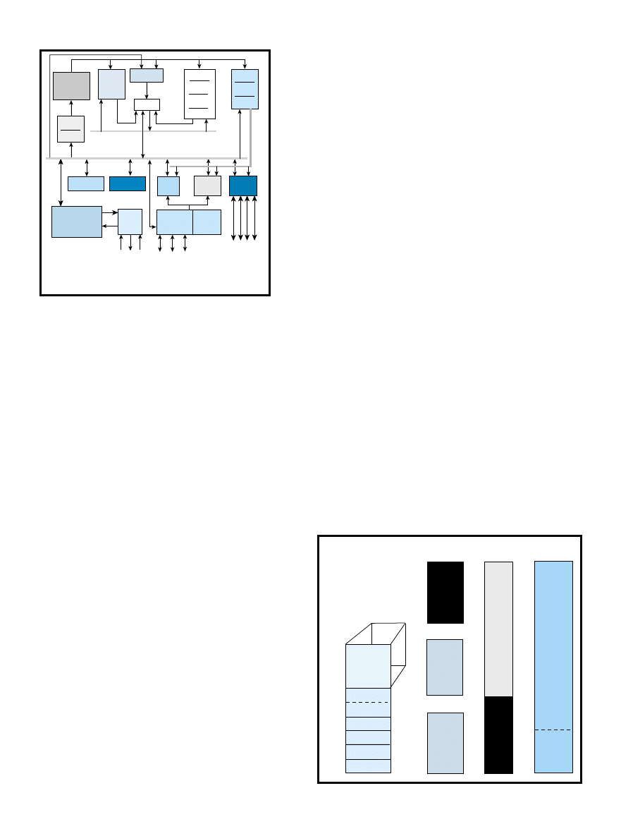
CIRCUIT CELLAR
®
Issue 127 February 2001
81
www.circuitcellar.com
External
data
memory
External
program
memory
8K x 8
Flash
memory
program
8K x 8
Flash
memory
program
128 bytes
Indirect
addressing
Bit addressable
Bank 3
Bank 2
Bank 1
Bank 0
FF
80
7F
2F
20
1F
00
Unusable
if internal
SRAM
is activated
1K X 8
SRAM
Data OR
prog mem
addr from
400-7FF
Internal
memory
03FF
0000
3FFF
2000
1FFF
0000
Internal
registers /
Scratch
pad
FFFF
FFFF
4000
0000
0000
03FF
Note: The black areas
shown on the internal
and external memory
are disabled on
powerup (default).
That is, until Dallas Semiconduc-
tor stepped up to the plate with its
’C320, a complete redesign that
boosted 8-bit MIPS dramatically.
Not that the majority of 8-bit appli-
cations need super-high performance.
But many will, and more importantly,
some of them can use all available
MIPS. In essence, the ’320 raised the
bar for 8-bit designs and reassured
designers that the headroom would be
there, as subsequently proven by the
response of other suppliers with their
own higher performance chips. In-
stead of an 8-bit market decline, the
’320 signaled a second wind that per-
sists to this day as more parts emerge
to serve more applications.
CLARK KENT
Looking at Figure 1, you would
never guess that the ’420 is a super
’51. It has the pinout and standard I/O
functions (three 16-bit timer and
counters, a serial port, and four 8-bit
I/O ports) that harken back to the
original. In addition, it has the selec-
tion of new-school peripherals, includ-
ing a second UART, watchdog timer,
and power monitor, which have be-
come standard in ’51 upgrades over
the years. The mild mannered appear-
ance extends under the hood (see Fig-
ure 2) where, except for a bit more
RAM and the use of flash memory,
little appears changed from the origi-
nal disco-era chip.
However, put the ’420
in a phone booth and out
comes an MCU that can
leap tall sockets in a
single bound. The ’420
easily takes the ’51 speed
crown and is, in fact, one
of the fastest 8-bit chips
you can buy.
MIPS MASTER
For a particular archi-
tecture, there are only
two ways to increase raw CPU perfor-
mance by implementation, reduce the
number of clocks per instruction or
boost the clock rate. The ’C420 does
both of these.
As with the ’320 and other suppli-
ers’ hopped-up ’51 designs, the ’420
takes an easy shot at the leisurely 12-
clock machine cycle of the original.
The ’320 took it from 12 clocks down
to three and the ’420 cuts the machine
cycle to a single clock.
At the same time, the clock rate of
the ’420 is boosted to 50 MHz. Be-
tween the machine cycle and clock
rate speedup, right off the bat you’re
looking at something like a perfor-
mance improvement of five times
more than the ’320, which is no
slouch itself.
I will forgive the marketeers ahead
of time for calling it 50 MIPs (for they
surely will). That’s the peak rate for
the fastest instructions, but your
mileage will vary. A closer examina-
tion of the ’420’s detailed instruction
timing sheds more light on the perfor-
mance story.
Within the constraints imposed by
the CISC ’51 architecture, various
factors determine ’420 instruction
timing. With an 8-bit bus, the absolute
minimum number of clocks an instruc-
tion takes to execute is the number of
opcode bytes (variable length, one to
three bytes). That minimum number
of clocks applies for instructions that
access registers or immediate data,
but instructions that require a
memory access add a clock. For ex-
ample, the instruction to increment a
register takes one clock and the in-
struction that increments a memory
location pointed to by a register takes
two clocks, though both are single-
byte opcodes.
Branches are always MIPS-deraters
and the ’420 is no exception. Depend-
ing on the particular flavor, they range
from two clocks for short and simple
branches up to five clocks for the most
CISC variants (such as those that com-
pare with memory or check and set a
Control
and
sequencer
Decoder
IR
Internal
registers
Interrupt
CPU
DPTR1
SP
PC
AR Inc
AR
Serial
I/O
Timer/
counters
Watchdog timer
and
power manager
Clock
and
reset
1K x 8
RAM
16K x 8
flash
I/O
Ports
Memory ROM
control loader
Internal control bus
XT
AL1
XT
AL2
RST
*PSEN
*EA
ALE/*PR
OG
P0
P1 P2
P3
Address
b
u
s
SFRs
DPTR
Figure 2—
Under the hood, the
’420 still looks a lot like a ’51 of
yore, except for the memory,
which is larger, faster, and
flashier.
Figure 3—
In addition to
the traditional 256 bytes
of scratchpad/SFR RAM,
the ’420 includes two 8-KB
blocks of flash memory and
an extra kilobyte of SRAM.
Notice that the SRAM can
function as data-only or
data and program depend-
ing on the address (0–
0x3FF is data-only and
0x400–0x7FF is data and
program).
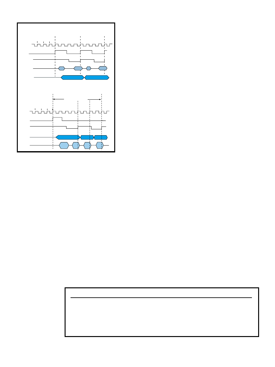
82
Issue 127 February 2001
CIRCUIT CELLAR
®
www.circuitcellar.com
Internal memory cycle
Ext memory cycle Ext memory cycle
XTAL1
ALE
*PSEN
Port 0
Port 2
MSB Add
MSB Add
C1 C2
C3
C4
C1 C2 C3 C4
LSB Add
Data
LSB Add Data
Internal memory cycle
Page miss
XTAL1
ALE
*PSEN
Port 0
Port 2
LSB Add
LSB Add
C1 C2
C3
C4
C1 C2 C1 C2
Ext code fetches
Page hit Page hit
LSB Add
MSB
add
Data
Data
Data
The most obvious fix for the ’51 is
to bypass the infamous DPTR (data
pointer) bottleneck. The bottleneck
occurs because the only way to access
external memory on a ’51 is via a
single DPTR register. The DPTR
stores the 16-bit memory address.
Even the simplest data movements,
such as a block move fill or copy, call
for torturous shuffling of addresses
into and out of DPTR.
Worse yet, although there’s an in-
struction to increment the DPTR,
there isn’t one to decrement it. Short
of brute force with explicit byte-wise
moves and subtracts, DPTR is a one-
way street.
This seemed so goofy that I actually
asked one of my former colleagues who
was involved with ’51 design about it.
Check out Figure 2 again and you’ll
find a clue to answer this techno-
trivia question.
Dallas tackles the challenge with
embellishments that go beyond
merely adding an extra DPTR register
like others have done before. Yes, an
extra DPTR allows you to keep track
of two addresses without a lot of shuf-
fling around, but you still have to
mess with selecting which one is
active, not to mention incrementing
it, or worse, decrementing.
Recognizing the opportunity to
further refine the dual DPTR idea,
Dallas adds automatic toggle and incre-
ment and decrement features. In es-
sence, the result is a kind of soft
DMA controller. For example, when
everything is set up (DPTR addresses,
DPTR toggle, increment/decrement
options, and byte count), the inner
loop of a block move routine boils
down to three instructions (two
MOVX instructions and a DJNZ),
which is much faster than a tradi-
bit). Note that, unlike many other
architectures, the timing for a condi-
tional branch is the same whether it’s
taken or not.
Of course, MUL and DIV take
longer at nine and 10 clocks, respec-
tively, but that is actually speedy
compared to other 8-bit chips, many
of which do not even come with the
handy numeric instructions in the
first place.
The only wart I could find was a
paragraph in the ’420 datasheet assert-
ing that one additional clock cycle
“may” be required if some control
registers (e.g., PSW, SP, IE) are written
to by certain direct addressing instruc-
tions. Also, there is one exception to
the fixed conditional
branch timing men-
tioned above. The
JBC instruction
(which tests and, if
taken, clears a bit)
takes an extra clock
(five versus four) if
the bit is cleared and
resides in one of the
aforementioned
control registers.
Just remember to keep
in mind that although
every ’420 instruction is
much faster than its ’51
counterpart, the speedup
is not the same across the
board. For instance, on the
’51 the
MOVX A,@DPTR
and
MOV direct,direct
instructions require two
machine cycles, each with
12 clocks, for a total of 24
clocks. For the ’420, the
former takes as little as
two clocks (assuming one
clock memory access) and
the latter takes three. The
different relative speedup
is something that should
be considered by those
people interested in opti-
mizing code specifically
for the ’420.
POWER POINTERS
Except for the usual
caveats about application-
specific timing, the move
to ’420 is an effortless upgrade (i.e., it
runs existing ’51 code without
change). However, every CPU de-
signer knows that beyond better
implementation (i.e., fewer and faster
clocks), the only way to boost perfor-
mance is to enhance the architecture
itself, which means the software must
change to exploit new features.
If the software has to be upgraded,
so be it. The challenge for the CPU
designer is to maximize the perfor-
mance gain and minimize the pro-
grammer pain associated with the
required tweaks. For example, it helps
if the software mods are relatively few
and isolated, and don’t require top-to-
bottom tool chain upgrades.
Figure 4—
The basic external access cycle requires four clocks
(a)
but a new page mode (b) cuts that to one or two clocks when
the MSB of the current cycle is unchanged from the previous one
(i.e., a hit within a 256-byte page).
Level
LB1
LB2
LB3
Protection
1
1
1
1
No program lock. Encrypted verify if encryption array is programmed.
2
0
1
1
Prevent MOVC in external memory from reading program code in
internal memory. EA is sampled and latched on reset. Allow no further
parallel or program memory loader programming.
3
X
0
1
Level 2 plus no verify operation. Also prevent MOVX in external memory
from reading internal SRAM.
4
X
X
0
Level 3 plus no external execution.
Table 1—
’420 security options, vital for flash memory micros, are arranged in a hierarchy from none, to encryption, to complete
internal access prohibition.
a)
b)

tional ’51. The ’420 is uniquely well-
suited for blasting data compared to
other 8-bit chips.
FAST AND SLOW
Getting the MIPS on the road starts
with the clock. The ’420 allows the use
of an external crystal at either one
quarter or half the clock rate (i.e., it
incorporates a flash memory option
bit that selects a 2×/4× clock multi-
plier). That solves the problem of
getting to 50 MHz using a commodity
(
²12.5-MHz) crystal. Following the
trend, the ’420 also includes an inter-
nal RC oscillator (nominally 10 MHz)
for applications that don’t demand
accuracy and to provide fail-safe
backup for the external clock.
The built-in flash memory and
SRAM (see Figure 3) can keep up, so
as long as you stay on-chip, there’s no
speed penalty. Going off-chip is when
things get interesting.
The original ’51 makes no allowance
for variable access time (i.e., there isn’t
any way to insert wait states). At the
time of its introduction, that wasn’t a
problem because the original 1-MIPS
’51 was so slow that it simply didn’t
put much stress on external chips.
Today though, it certainly wouldn’t
be a good idea to require that anything
and everything you might want to
connect to a 50-MHz ’420 have a 10-ns
access time. Indeed, a particular system
might well include a mix of very fast
and very slow chips.
In general, a ’420 external bus cycle
(see Figure 4a) requires four clock
cycles (e.g., 80 ns at 50 MHz). To
accommodate speed freaks, there’s
also a page mode (see Figure 4b) that
cuts external accesses to one or two
clocks for a page hit and two or four
clocks for a page miss, respectively.
At the same time, external data ac-
cesses can have programmable stretch
cycles up to dozens of clocks.
In fact, as a MEDITATE alternative
to the usual, clock-stopping, low-
power SLEEP modes, the ’420 clock
has a divide-by-1024 option. Drifting
along at a slow speed can save power
without the overhead and delays of
hopping in and out of bed. If you com-
bine the 1024 clock divider with the
stretch cycle stuff, you can practically
see the pins wiggling with your bare
eyes (i.e., bus cycles that take hun-
dreds, even thousands of clock cycles).
I’m pleased with the progress all
the MCU suppliers are making in the
universal migration to on-chip flash
memory. Dallas is no exception, and
its flash memory includes all the in-
system and self-programming features
a designer could ask for, including
four, count ’em four, security modes
(see Table 1) that will most definitely
keep the code pirates at bay.
Naturally, software can program
the chip in operation. The 16-KB flash
memory is organized as two 8-KB
banks, one of which contains the code
that runs to program the other. The
programming operations themselves
are completely self-timed and well-
hardened against foul-ups with protec-
tion mechanisms such as keyed access
to critical control bits.
The ’420 also adopts the latest
trend with a built-in boot ROM fea-
ture that allows programming through
SOURCE
DS89C320, DS89C420
Dallas Semiconductor Corp.
(972) 371-4448
Fax: (972) 371-3715
www.dalsemi.com
Tom Cantrell has been working on
chip, board, and systems design and
marketing for several years. You may
reach him by e-mail at
tom.cantrell@circuitcellar.com.
a standard serial port for easy initial-
ization out of the tube and subsequent
field upgrades.
Finally, the ’420 even supports the
historic (à la EPROM/OTP) parallel
mode that works with the typical
PROM programmer most designers
already have in hand, as well as high-
volume production gang-programmers.
KEEPING ON AND KEEPING UP
With the ’420, Dallas has once again
demonstrated its flair for innovation
and the means and will to make it
happen. Maybe your current designs
don’t need such a fancy chip, but it’s
nice to know the ’420 is there if your
next design calls for a little more juice.
Dallas may not be a Fortune 500
powerhouse, but it deserves credit for
mounting a credible challenge against
the big guns. In my opinion, the ’420
can go head-to-head with the best the
competition has to offer.
Although the market remains stron-
ger than ever, the new ’420, like the
’320 before it, provides comforting
reassurance that as far as the 8-bit
market and the venerable ’51 goes, it’s
still onward and upward.
I
Problem 2
—
In the more general case, show
that divides evenly for positive integers n.
Problem 1
—
There’s a really simple way to demonstrate
that the quantity is an integer as long as A and n are integers.
What is it?
CIRCUIT CELLAR
Test Your EQ
CIRCUIT CELLAR
What’s
your EQ?
—The answers and 4
additional questions and answers are
posted at www.circuitcellar.com.
You may contact the quizmasters
at eq@circuitcellar.com.
8
more EQ
questions
each month in
Circuit Cellar Online
(see pg. 4)
Problem 3
—
Can you show that
2222
5555
+ 5555
2222
is divisible by 7?
Problem 4
—
Why doesn’t the windchill effect cause a car’s
climate-control system to get confused about the outside air
temperature when moving at highway speeds?

CIRCUIT CELLAR
®
Issue 127 February 2001
95
www.circuitcellar.com
Page
94
Abacom Technologies
90
Ability Systems Corp.
93
ActiveWire, Inc.
16
ADAC
8,58
Advanced Transdata Corp.
35
All Electronics
94
Amazon Electronics
9
Amulet Technologies
85
Andromeda Research
94
AP Circuits
40
Arcom Control Systems
56,57
Atmel Corp.
44
Avocet Systems
93
Bagotronix
85
Basic Micro
90
CCS (Custom Computer Services)
64,94
Ceibo
92
Cermetek Microelectronics, Inc.
88
Circuit Specialists
11,89
Connecticut microComputer, Inc.
93
Conitec
91
Copeland Electronics, Inc.
94
CSMicro Systems
93
Cyberpak Co.
25
Cygnal Intergrated Products
89
Data Design Corp.
C4
Dataman Programmers, Inc.
88
Decade Engineering
7
Design Logic 2001Contest
ADVERTISER’’’’’S
INDEX
92
Lynxmotion, Inc.
41
Marlin P. Jones & Assoc. Inc.
92
MCC (Micro Computer Control)
84
MetaLink Corp.
87
Micro Digital Inc
92
MicroEngineering Labs, Inc.
79
Micromint, Inc.
50
Midwest Micro-Tek
63
Miller Freeman
88
MJS Consulting
10,30
MVS
31
NetBurner
33,94
NetMedia Inc.
77
Newnes
84
Nohau Corp.
59
Ontime
90
Ontrak Control Systems
C2
Parallax
92
PCB Express, Inc.
87,90
P & E Microcomputer Systems
84
Phytec
88
Phyton
93
Picofab, Inc.
91
Prairie Digital, Inc.
88
Pulsar, Inc
23
Rabbit Semiconductor
65
Remote Processing
85
R.E.Smith
89
RLC Enterprises, Inc.
Page
Page
The Advertisers’ Index with links to their web sites is located at www.circuitcellar.com under the current issue.
92
RMV Electronics, Inc.
69
Saelig Co.
5
Scott Edwards Electronics, Inc.
90
Senix Corp.
94
Sigg Industries, Inc.
84
Signum Systems
90
Silverline Power Conversion
91
Sirius microSystems
91
SMTH Circuits
89
SmartHome.com
26
Solutions Cubed
84
Square 1 Electronics
50
Tal Technologies
17,49
Technologic Systems
93
Technological Arts
C3
TechTools
87
Tern, Inc.
11
Trilogy Design
86
Vetra Systems Corp.
55
Virginia Tech Transport Inst.
85
Virtual Tools, Inc
93
Weeder Technologies
1
Wilke Technology GmbH
91
Xilor Inc.
89
Z-World
92
Zanthic Technologies Inc.
71
ZiLOG
Page
Homegrown:
An Organic Robot Project
Take Your Base:
A Mobile Robot Platform
From the Oil Field to Your Home:
The Geo-Mite
Steplocked Magic Sinewaves
I Embedded Living:
Wire is Passé
I From the Bench:
Getting a Grip on Complex Integration—Looking at FPSLIC
I MicroSeries:
Fundamentals of Second-Order Systems—Part 3
I Silicon Update:
SoC Hop
EPC
Applied PCs:
Launching E-Mail
Robotics
PREVIEW
128
87
Designtech Engineering Co.
86
Digital Products
89
Diversified Engineering
86
Diversified Enterprises
18
DreamTech Computers
34
ECD (Electronic Controls Design)
54
Earth Computer Technologies
85
EE Tools (Electronic Engineering Tools)
90
Electronic Systems Consulting
86
Elk Products
48
EMAC Inc.
34
Engineering Express
85
FDI (Future Designs, Inc.)
17
General Software
85
Hagstrom Electronics
91
HVW Technologies
90
Inicore
88
IMAGEcraft
87
IndustroLogic, Inc.
55,91
Intec Automation Inc.
74
Interactive Image Technologies, Ltd.
91
Intronics, Inc.
86
Island Logix
39
Jameco
65,87
JK microsystems
50
JR Kerr Automation Engineering
89
Laipac Tech
15,45
Lemos International
2
Link Instruments

www.circuitcellar.com
96
Issue 127 February 2001
CIRCUIT CELLAR
®
almost never discuss real-time political or social issues in my editorials. Yes, I discussed
the Napster ruling and Y2K concerns but I can’t remember ever running off at the mouth about
current events of a nontechnical nature. Well, call this a first if you must, but I feel the necessity to
come to the defense of those of us in the media (and I associate myself with those “other” guys in the
generic sense only) who aren’t ruled by hype and ratings.
What am I talking about? I’m referring to the media circus we Americans called a presidential
election last November (and December, etc). An article in the
New York Times pretty much summed it
up best for me. The article discussed how the media hyped up the situation to the point of frenzy, only
to counter those reports with the reassurance that, “there are no tanks in the streets.”
Why do I care? Why waste this space talking about it? Basically, the whole world watches CNN and
I’m irritated that we must have looked like a horse’s patuti!
Circuit Cellar has international readers and international advertisers. The perception that the U.S.
can degrade into a third-rate banana republic when something atypical happens in our election process
is not only a misconception, it’s an outright fabrication merely to hype ratings. It shouldn’t be miscon-
strued as reality.
We live in a global economy. National perception is important to the business of the country. Unfortu-
nately, perceptions that used to stop at the border are now shared with the rest of the world. For example,
whether or not the assessment is correct, the media portrayal of the discord between Israelis and
Palestinians leads to an impression of anarchy. It may all be righteous indignation according to their
standards. Nonetheless, viewing that situation from this end surely doesn’t cultivate thoughts of expanded
business investment in the area.
When I was debating whether or not to write about all this, I decided to look closer at
Circuit Cellar’s
demographics. Although our foreign print circulation has always hovered around 20% (it will be expanding
considerably with
Circuit Cellar’s new electronic edition), the extra-territorial traffic on our web site is
considerably higher, at 35% to 40%. Expanding
Circuit Cellar within the foreign technical community is
about enhancing the perception that we have something to offer them, not fighting the misconception that
we’re a bunch of yahoos over here.
To the rest of the world, American freedoms can seem like a conflicting mix. Americans can own
guns, burn the national flag, and do things in the name of freedom of the press and speech that would
appear vile to any sane human being. At the same time, and viewed without the prejudice of similarly
over-hyped events in the past, there is a responsibility to use those freedoms wisely and in the
common interest. The fact that one freedom gives us the power to radically oppose another doesn’t
mean that we expect to use it that way. The fact that “your” guy didn’t get elected or that it took a court
decision to decide an election didn’t cause an uprising. It served only to reestablish the rule of law, not
the rule of anarchy.
I apologize for a news media that falsifies reality to promote itself. Rest assured, when all of us here
are saying “praise the Lord and pass the ammunition” it will be for something a lot bigger than an
election.
PRIORITY
INTERRUPT
steve.ciarcia@circuitcellar.com
So, Where Were the Tanks?
i
Wyszukiwarka
Podobne podstrony:
circuit cellar2000 02
circuit cellar1995 02
circuit cellar1991 02,03
circuit cellar1994 02
circuit cellar2003 02
circuit cellar2004 02
circuit cellar2002 02
circuit cellar1993 02
circuit cellar1997 02
circuit cellar1990 02,03
circuit cellar1996 02
circuit cellar1992 02,03
circuit cellar2000 02
circuit cellar1992 02,03
circuit cellar1993 02
circuit cellar1991 02,03
circuit cellar1994 02
więcej podobnych podstron