W
ords are wonderful in their ability to form vi-
sions and emotions in our minds. Such a simple word as
“home” can, with itsassociations, bring a tear to a weary
traveler’s eye. Other words, take
can produce fevered visions of technology oozing from the
very pores of casinos while armies of disembodied feet
plod through aisles stretching to infinity..
Can you tell that I just finished “doing” COMDEX? A
week of strolling past the latest in microcomputers has left
me tired and footsore, but encouraged about the future of
the small computer industry.
MS-DOS MARCHES ON...
.
more accurately, the Intel
family keeps
rolling. The perception of the 80x86 as an architecture for
desktop business machines only is in the process of radical
change. While there were scads of computers for running
spreadsheets and word processors, I sawconsiderable evi-
dence of the 80x86 becoming a leader in the application
and control markets. In one form or another, the Intel
architecture was the dominant force at almost every level.
First, the high end: You couldn’t swing a dead cat
without hitting an 80486 motherboard at COMDEX. Of
entirely, and all the 80486s to be found had major bugs of
one flavor or another. No matter, the manufacturers have
decided that 80486 is the way to go, so the clones were out
in force. Most of the “clone” motherboards used the ISA
(PC/AT) bus, and many proclaimed EISA compatibility.
Since the EISA
is still a darker secret than the avionics
in the B-2, I don’t know whether or not any of the EISA
machines work as promised. In any event, the 80486
machines are being sold as the microcomputers that will
finally bring about the demise of minicomputers. Sales
folks talk about the 80486 as the perfect processor for LAN
servers, but the winks and nudges on the side say that no
high-powered engineer, programmer, or financial analyst
is going to be satisfied until a fire-breathing 80486 com-
puter with 600-MB hard disk, 16 MB RAM, 8514A graph-
ics, and
price tag is enshrined on his or her desk.
The favorite pastime of computer industry pundits is
proclaiming the death of the 80286. Since everyone knows
how deficient the processor is, you wouldn’t have ex-
pected to see any major moves in the 80286 market. In my
view, though, one of the most exciting products of the
show was the 80286 plug-in module from Mitsumi. The
module puts an
memory, and all of the “glue”
chips for a working AT-type computer into a package only
slightly larger than an 80486. The engineers at Mi tsumi see
the 80286 playing an increasing role in embedded applica-
tions, and they are pushing the idea of the entire computer
as a plug-in module. According to the engineers, fax
machines have already been designed around their 80286,
and more products are on the way. I think they may be on
to something with this approach, and we’re working on an
article showing how to use the module in applications.
A side-effect of the 80286’s move into embedded
applications may be the demise of the 80186. The ‘186 has
been a favorite of designers who wanted to develop soft-
ware under MS-DOS but needed more oomph than an
8088 could muster. Products like the Mitsumi module
make it much harder to justify the 80186 approach.
Finally, the time has arrived for XT-class machines to
take a serious role in the control application market. I
know: “Real”computer people hate thearchitecture, loath
the operating system, and can’t abide the lack of built-in
I/O.
thatmatters when
you
can
buy
a full IO-MHz
XT motherboard for
(quantity
At that price, eco-
nomics begin to cast a rosy glow over most shortcomings.
Several months ago I wrote about the move toward
using PC-type computers for control applications. The
trends I saw at COMDEX tell me that the trend is acceler-
ating. Good software development tools and low hard-
ware costs are teaming up to make the Intel/MS-DOS
combination irresistible to a lot of developers.
What does all of this mean for other microprocessors
and controllers?
Other
architectures won’t wither just be-
cause of new competition. We’ll see a push to bring
software development tools to a new level of functionality
and friendliness. Engineers and programmers have toler-
ated obtuse commands and low functionality in microcon-
troller development tools because “that’s the way it’s
always been done.” Users accustomed to the “look and
feel” of the best MS-DOS compilers and other develop-
ment tools, will push the software vendors to give them
better tools. If the vendors are smart, they won’t argue.
February/March
1
FOUNDER/
EDITORIAL DIRECTOR
Steve
Ciarcia
PUBLISHER
Daniel Rodrigues
EDITOR-in-CHIEF
Curtis Franklin, Jr
PUBLISHING
CONSULTANT
John Hayes
ENGINEERING STAFF
Ken Davidson
Jeff Bachiochi
Edward
y
CONTRIBUTING
EDITORS
Thomas
Jack Ganssle
CONSULTING
EDITORS
Mark Dahmke
Larry Loeb
CIRCULATION
COORDINATOR
Rose Manse/la
CIRCULATION
CONSULTANT
Gregory
ART PRODUCTION
DIRECTOR
PRODUCTION
ARTIST/ILLUSTRATOR
Lisa Ferry
BUSINESS
MANAGER
Jeannette Walters
NW PRODUCTS
EDITOR
Harv Weiner
STAFF RESEARCHERS
Northeast
Eric
William
w
Richard Sawyer
Robert
Midwest
Jon
Tim
West Coast
Frank Kuechmann
Mark Voorhees
Cover Illustration
by Robert Tinney
THE COMPUTER
APPLICATIONS
JOURNAL
21
42
Building etude:
Part 1
A 25-MHz Analog-to-Digital Convertor for the PC Bus
by J. Conrad Hubert and Dick Hubert
It’s hard to imagine doing serious data
acquisition without a serious digitizer.
The etude
board is just
that. The first of two parts deals with
the hardware side of the story.
The BCCH 16
Part 2
Porting a Multitasking BASIC to the H 76
by Jack Ganssle
The BCCH 16 is more than hardware: a multitasking BASIC compiler lets you
put its power to use. Jack Ganssle looks at the process of porting a compiler
between similar processors in the wrap-up article on the BCCH 16.
Editor’s INK
Dateline: Las Vegas
1
by Curtis Franklin,
Reader’s
to
the Editor
NEW
Product News
Visible INK-
Letters to the INK Research
Firmware Furnace
An Exercise for the Student
Building Software from fhe Ground Up
by Ed
5
8
12
52
From the Bench
. . . ATTENTION . . . ATTENTION ATT
Building an LED Moving Message Display
by Jeff
60
2
CIRCUIT CELLAR INK
Circuit Cellar BBS-24
Hrs.
bps, 8
bits, no parity, 1 stop bit,
871-1988.
The schematics pro-
vided in Circuit Cellar INK
are drawn using Schema
from Omation Inc. All pro-
grams and schematics in
Circuit Cellar INK have
been carefully reviewed
to ensure that their per-
formance is in accor-
dance with the specifica-
tions described, and pro-
grams are posted on the
Circuit Cellar BBS for elec-
tronic transfer by subscrib-
ers.
Circuit Cellar INK
makes no warranties and
assumes no responsibility
or
of any kind for
errors in these programs or
schematics or for the con-
sequences of any such
errors.
Furthermore, be-
cause of the possible vari-
ation in the quality and
condition of materialsand
workmanship of
assembled projects, Cir-
cuit Cellar INK disclaims
any
for the
safe and proper function
of reader-assembled proj-
ects based upon or from
plans. descriptions, or in-
formation published in
Circuit Cellar INK.
Digital Signal Processing
Part
An Introduction
by Dean McConnell
Digital Signal Processors
have changed the way we look
at analog signal problems. In the
first of two parts, Dean McConnell
discusses the most commonly
used transforms and how they’re
applied.
Building An IBM PC Keyboard Translator
An 803
System for Code Translation
by Bill Curlew
You
know the problem: You have a favorite
keyboard, but it only works with one of your
systems. Wouldn’t it be nice if you could
take “old reliable” with you as you move
from system to system? With the keyboard
translator developed by
Bill
Curlew, you can!
Advertiser’s Index
65
Silicon Update
Earthshaking Chips
68
A Report from the Second Microprocessor Forum
by Tom
Software by Design
Memory Management on the HD64180
by Jack
72
from fhe Circuit Cellar
Conducted by Ken Davidson
76
Steve’s Own INK
An Analog State of Mind
by Steve Ciarcia
80
CIRCUIT CELLAR INK
08968985) is pub-
lished bimonthly by Circuit
06066
875-275
Second-class postage
paid at Vernon, CT and
additional offices.
year (6 issues) subscription
rate U.S.A. and possessions
S14.95, Canada 17.95, all
other countries $26.95. All
subscription orders pay-
able in U.S. funds only, via
international
postal
money order or check
drawn on U.S. bank. Di-
rect subscription orders to
Circuit Cellar INK, Subscrip-
tions, P.O. Box 2099,
hopac. NY 10541 or call
875-2 199.
Please
send address changes to
Circuit Cellar INK. Circula-
tion Dept.. P.O. Box 2099.
Mahopac, NY 10541.
Entire contents copy-
right 1990 by Circuit Cellar
Incorporated. All rights re-
served. Reproduction of
this publication in whole
or in part without written
consent from Circuit Cel-
lar Inc. is prohibited.
February/March
3
READER’S
INK
letters to the Editor
TAKE CONTROL
I really enjoy reading
C
ELLAR
After deal-
ing with multiprocessing super-mini control computers
that only a rocket scientist would understand while at
work, it’sgreat to know thereisstilla
applications that don’t use megabytesof memory. I
enjoy reading the tutorials on embedded systems, both
hardware and software. The tutorials are of great value
when trying to integrate systems and people at work.
After staying on the sidelines for quite some time, I
now have something to contribute. This is a reply to
Snyder concerning motor control and track switch-
ing
C
ELLAR
INK 11).
Bruce Chubb has written a book called “Build Your
Own Universal Computer Interface,” ISBN O-8306-3122-4,
published by Tab Books. I have seen it in several book-
stores around the LA/Orange County area so I don’t
imagine it would be too hard to find.
The book describes (what else?) a universal interface
that will connect almost any computer through a bus or
serial port, analog and digital data acquisition and control,
interface testing, and control software, and ties it all to-
gether with a project involving model railroad control.
Kevin K. Asato
CA
EVEN FARTHER BEYOND
I appreciated Tom Cantrell’s article
(“Beyond
in C
IRCUIT
C
ELLAR
INK
Indeed, the
dollar PLD industry has grown dramatically since its
humble beginnings barely a decade ago, and the growth is
not slowing. The good news is that it is now becoming
economically
practical (and desirable) to design
with
and other
at home!
The
programmable
logic devices themselvesarecheap,
and PLD “starter kits” are now available for around $50
that provide good PC-based development software (albeit
limited to only a few device types). The final link-the
device programmer-is also now available from several
sources in the $300 price range.
With a few
around, and the appropriate devel-
opment software and hardware, home designers are no
longer at the mercy of their stock of “jellybean” parts
laying around. Need a 4-bit counter or a 9-input AND gate
with both inverted and noninverted outputs? Just pro-
gram your PLD to do what you need! Wiring up projects
is also much simpler with
since a single PLD can
often functionally replace several
SSI/MSI
devices. If your project doesn’t work, don’t change the
circuit, just change the PLD programming.
For
readers interested in more
information about
I suggest they check out my new book from Howard W.
Sams Co., “Programmable Logic Designer’s Guide,”
ISBN O-672-22575-1.
Roger C.
Dexter, MI
MORE ON MILDEW
I read with interest the letter from Guyana and your
response in
In June I attended the
first International Conference on Computing and Mis-
sions at Taylor University in Upland, Indiana, where the
same problem was discussed. The missionaries reported
that Tupperware makes an ideal container for preventing
formation of mildew on diskettes, especially with the
addition of silica gel as you suggested.
That conference was the first place I had heard of the
problem, so I’m not surprised at the discussion you had.
Duane Vosburg
Binghamton, NY
. ..AND FROM THE OTHER SIDE
I wish to protest in the strongest and most vociferous
terms the editorial focus and content of
C
ELLAR
INK
for which I have been forced to pay and accept, as a
subscriber.
With issue
“Build Your Own 386 Clone” (yeah, I’ll
run right out and do it), its “32-bit Multitasking
February/March
ler” (surely what every reader needs), and its “Design
Your Own 32-Node Network for Your EGA AT” (clearly
everyone’s goal), issue 11 is a serious breach of the spirit,
essence, and soul of the Circuit Cellar articles originally
appearing in BYTE.
Sir, it was the minimalist nature of the Circuit Cellar
articles which made the hardware they described charm-
ing, practical, comprehensible, affordable (in both time
and money), and, in a word, accessible.
That is what I imagined I was buying when I sub-
scribed to C
IRCUIT
C
ELLAR
INK. Please get back on track.
Edward
Madison Heights, WI
P.S. I understand you are seeking authors. I believe a
buddy of mine has an article entitled “How I Networked
my
Dozen VAX
to my Cray in my Spare Time For
Only $560,000.” Would you be interested in seeing it?
Thank you for
taking
the time to write with
your concerns
over
the content of
C
ELLAR
INK It’s always helpful
to
hear
from our readers.
We ty, here at C
IRCUIT
C
ELLAR
INK, listen to our
readers.
When a
number of readers write with the
same
request, that request receives additional priority. So if was
with
the
project, the single most requested topic
over
the last
18 months.
I assume, from
subtle clues in your letter, that you
appreciate projects based on the 8031 and 8052 microcon-
trollers. There have been a number
of
projects using these
controllers, and rest assured there will be more such projects in
the future.
might
mention that the control network article in
was based on the
troller.)
Our goal is to present a variety of projects balanced in
complexity and expense. Just as the Circuit Cellar column in
both largeandsmall projects (see theprojectsfor
the
CCAT, and Mandelbrot Engine
for
examples of
“large” projects),
C
ELLAR
INK will present projects
based on processors and controllers ranging from the cheap and
“accessible” to
the
challenging.
readers who need
bo
fh,
and we will ty to keep as many readers happy as is possible.
The “spirit, essence, and soul” of C
IRCUIT
C
ELLAR
INK are
defined by an attitude toward presenting working, practical
projects and tutorials, regardless
of
the processor, controller,
bus used. While your letter
makes
if sound
as though you will
our
planned projects
based
on
warn you
we
are
also planning
fs
based
on the 68000,
80286‘32532, and other
“large” processors and controllers.
Curtis Franklin, Jr.
P.S.
Please
have your buddy
forward an
outline
of his project.
we
can
work
a
hack to dangle an 8033 controller off one of the
nodes, we
might just have a
winner.
NOW
PERFORMANCE
L A C E Y O U R X T / A T M O T H E R B O A R D
W I T H A 2 M B P I
F O R O N L Y
l
Made in America
l
8.5” x 13”
Fits XT, Baby or Full AT Tower cases
l
and Shadow BIOS Support
l
Choice of
or
BIOS
l
or
models available, up to
8MB RAM
l
Three years parts and labor Warranty
l
25-33 MHz
motherboards also
available with/without SRAM cache
Inc.
1030
Earlysville Forest Drive
Charlottesville, VA 22936
o n l y 8 0 0 - 6 6 6 - 9 2 4 8
Information and
804-978-3917
Tech Support;
Fax: 804-978-3906
Reader Service
6
CELLAR INK
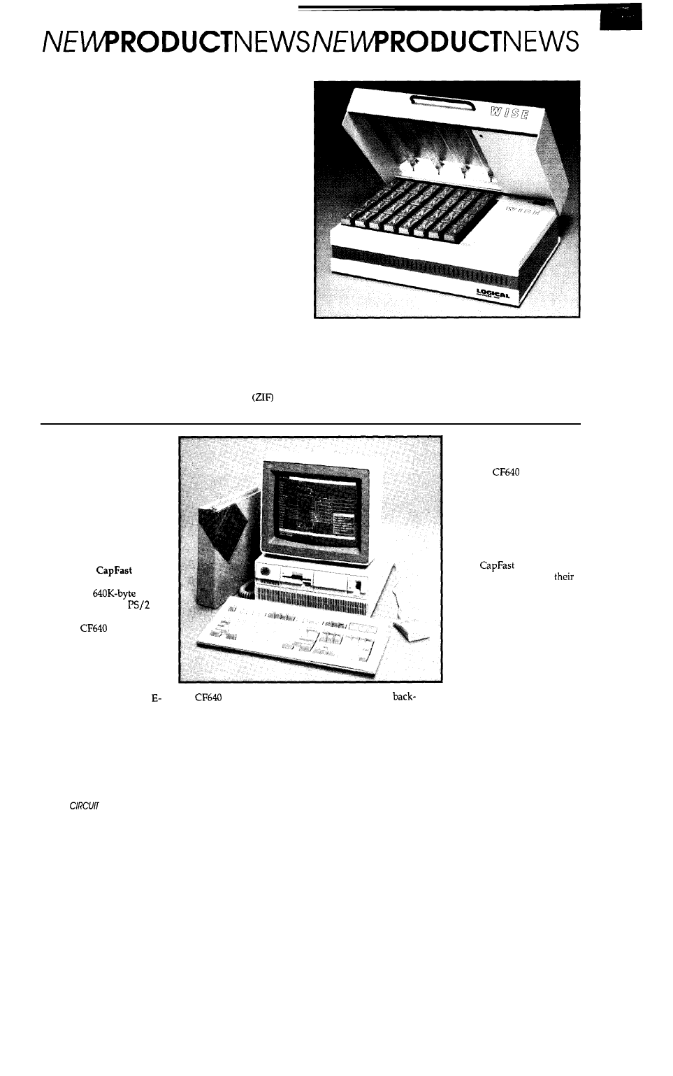
EPROM ERASER/PROGRAMMER SYSTEM
The need for a separate gang programmer and eraser
lamp has been eliminated with the announcement of the WISE
EPROM
Erased Programmer
system by Logical Devices Inc.
WISE allows the user to insert EPROMs into the programming
sockets and initiate an erase/program cycle with a single push
button. EPROMs are first erased by exposure to an ultraviolet
(UV) light source located in the top lid of the unit. A patented
Proprietary Intelligent Erasing Algorithm determines a safe
erasure time. After erasure, the programmer automatically
deactivates the UV light and begins the programming cycle.
With conventional programming systems, EPROM
erasure is performed as a separate step. Devices are placed
under an eraser lamp for an estimated erasing time. The
devices are then removed from the eraser and placed into a
programmer. The programming system must check to see if
the devices are blank to avoid errors. If they are not, the
devices must undergo another erasure and check cycle.
While the UV erasing system is operating, the program-
ming section of the unit will read the data in each one of the 32
chips on a repetitive basis to monitor the exact time to erase all
of the EPROMs. The system will abandon faulty chips that
will not erase within a specified time in order to avoid system
hangups. Erasure time is done at Vcc margins and a safety
erasing time is allowed to avoid fading of EPROMs.
As a further time saver, the WISE system also uses a
solenoid-activated, auto-load Zero Insertion Force
socket
handle flipper. This eliminates the need to individually lift
and close the ZIF socket handles. The WISE
system
is priced
at $9995.
Logical Devices, Inc.
1201 NW 65th Place
Ft. Lauderdale, FL 33309
(305) 974-0967
LOW-COST
SCHEMATIC DESIGN
PACKAGE
Phase Three Logic Inc.
has announced a low-cost
schematic design package de-
veloped for the broad
electronic-design automation
market.
The
CF640
Schematic Design Package
runs on the
main
memory of PC/AT,
and
compatible systems.
The
uses an
incremental design concept
combined with an overlay
memory management system
to handle large designs with
multiple pages. It can handle
an individual A- through
size schematic page and
extract a net list for a SO-page
design with C-size pages (ap-
proximately 10,000 design
elements).
In addition to the
incremental net list extractor,
8
CEL LAR INK
the
Schematic Design
Package includes an intelli-
gent packaging program that
automatically assigns
reference designators and pin
numbers to physical pack-
ages, Xilinx and Abel inter-
faces and symbol libraries,
and a PADS-PCB
annotator. It also includes
the symbol creation editor, an
enhanced symbol library
composed of more than 5500
parts, an incremental part list
program, Spice interface
tools, Susie digital simulator
interface, and interfaces to
major PCB-CAD systems.
The
provides up
to four split-screen windows
for simultaneous global and
local viewing and features
infinite zoom levels.
Hardcopy printer and plotter
support is also provided. The
system may be upgraded to
other
software
products because all of
design databases are 100%
compatible. This growth
path extends to Sun Worksta-
tion Unix versions.
The CF640 Schematic
Design Package is priced at
$295 and includes a 30day
money back guarantee. One
year of software updates and
support is included at no
charge.
Phase Three Logic, Inc.
1600 N.W. 167th PI.
Beaverton, OR 97006
(503) 645-0313
NEWPRODUCTNEWSNEWPRODUCTNEWS
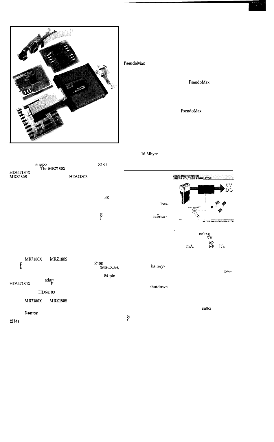
IN-CIRCUIT EMULATORS SUPPORT ENTIRE 2180
AND HD64180 FAMILY
Macrochip Research is now offering low-cost in-circuit
emulators that
rt the newest members of the
and
HD64180 family.
he
emulates Hitachi’s
ZTAT (Zero Turn Around Time) device, and the
emulates Hitachi’s new
HDLC serial
controller device. Both emulators connect to the PC’s serial
port and provide real-time, nonintrusive in-circuit emulation
with no wait states at clock speeds up to 10 MHz. On-chip
refresh is maintained at all times. Both emulators feature 64K
bytes of emulation overlay memory, mappable on any
boundary within the first 64K physical address space.
A complete monitor/debugger, provided in firmware,
allows the user to assemble and disassemble code; examine
registers, memory, and I/O; set breakpoints; and sin
the target processor ROM or RAM without the use o
le step
special
driver software on the host. Intel hex or straight binary files
can be downloaded from the host directly into target memory
or overlay memory at serial rates up to 38.4 kbps.
_
The emulator allows up to four hardware breakpoints that
can be placed anywhere in the target system’s 1 megabyte
physical address space. Additionally, each breakpoint can be
qualified to break only on memory read, memory write, I/O
read, I/O write, opcode fetch, or interrupt acknowledge
cycles.
The
and
emulators are shipped with
an 84 in PLCC emulation plug, 6’ RS-232 cable,
macro
assem ler and Development Environment software
and user’s manuals. Options include HD64180 cross-assem-
blers for the Macintosh and Amiga computers, and an
PLCC to 28-pin DIP
s internal E
tor for programming the
ROM using an ordinary EPROM
programmer. Each of the emulators can be field converted to
emulate another
family member at a relatively low
price.
The
and
list price is $1995 each.
Macrochip Research, inc.
1301 N.
Dr., Suite 204
Carrollton, TX 75006
242 0454
68000 SIMULATOR ALLOWS
FULL MEMORY ADDRESSING
Testing and debugging
Motorola 68000 programs
before hardware is available
is now possible with the
68k simulator
from Pseudo Corp. The
developer can watch the
program execution via
machine windows as the
simulator single steps or free
runs through the program
code. Each register, the stack,
I/O ports, and blocks of
memory can be monitored.
User-definable screens
enable the designer to
customize the simulator.
Each screen can contain up to
40 machine-specific win-
dows. The simulator uses an
internal demand-page virtual
memory addressing algo-
rithm that allows simulation
of the full
address-
ing space. Simulations
include input/output
interrupts, traps, and excep-
tions. Other features include
unlimited breakpoints,
memory mapping, and a
trace file feature that allows
selective recording of the
simulator session for later
analysis.
requires a
512K IBM or compatible PC
with mono, CGA, EGA,
Hercules mono display and
MS-DOS 2.1 or greater. The
introductory price of the
68k is $100. The
68k
cross-assembler is
$50.
and a 68k disassembler is
available for $100.
The
Developer
Pack
consisting of
all three products is $200.
Pseudo Corp
P.O. Box 1423
Newport News, VA
23601-0423
(804) 595-3703
CMOS
MICROPOWER
VOLTAGE
REGULATORS
A new family of
cost micropower voltage
regulators, featuring an
optimized wafer
tion process, has been
announced by Teledyne
Semiconductor. The TSC663.
664, and 666 are lower cost
pin and functional replace-
ments for similar devices
from other manufacturers.
set with just two resistors.
The input
from 2 V to 16.
e can be
and the
The TSC663 positive
voltage regulator, and
TSC664 negative voltage
regulator are designed
particularly for
powered applications. They
feature low standby current
for low quiescent power, and
a shutdown pin for external
control. In the
mode, quiescent current is
less than 12 microamps. The
regulators are designed to be
used either as fixed 5-V
regulators with no external
components, or as adjustable
re ulators with output
vo tages from 1.3 V to 16 V
output current ca
40
These C
ability is
OS
are
very low noise, wide band-
width linear regulators, and
have output current limiting
built in.
The TSC666 is a positive
voltage regulator with a
battery detection circuit to
detect the input voltage drop-
ping below specification and
provide a signal to the system
to warn of impending power
loss.
Teledyne Semiconductor
1300 Terra
Avenue
Mountain View, CA
94039-7267
(415) 968-9241
February/March 1990 9
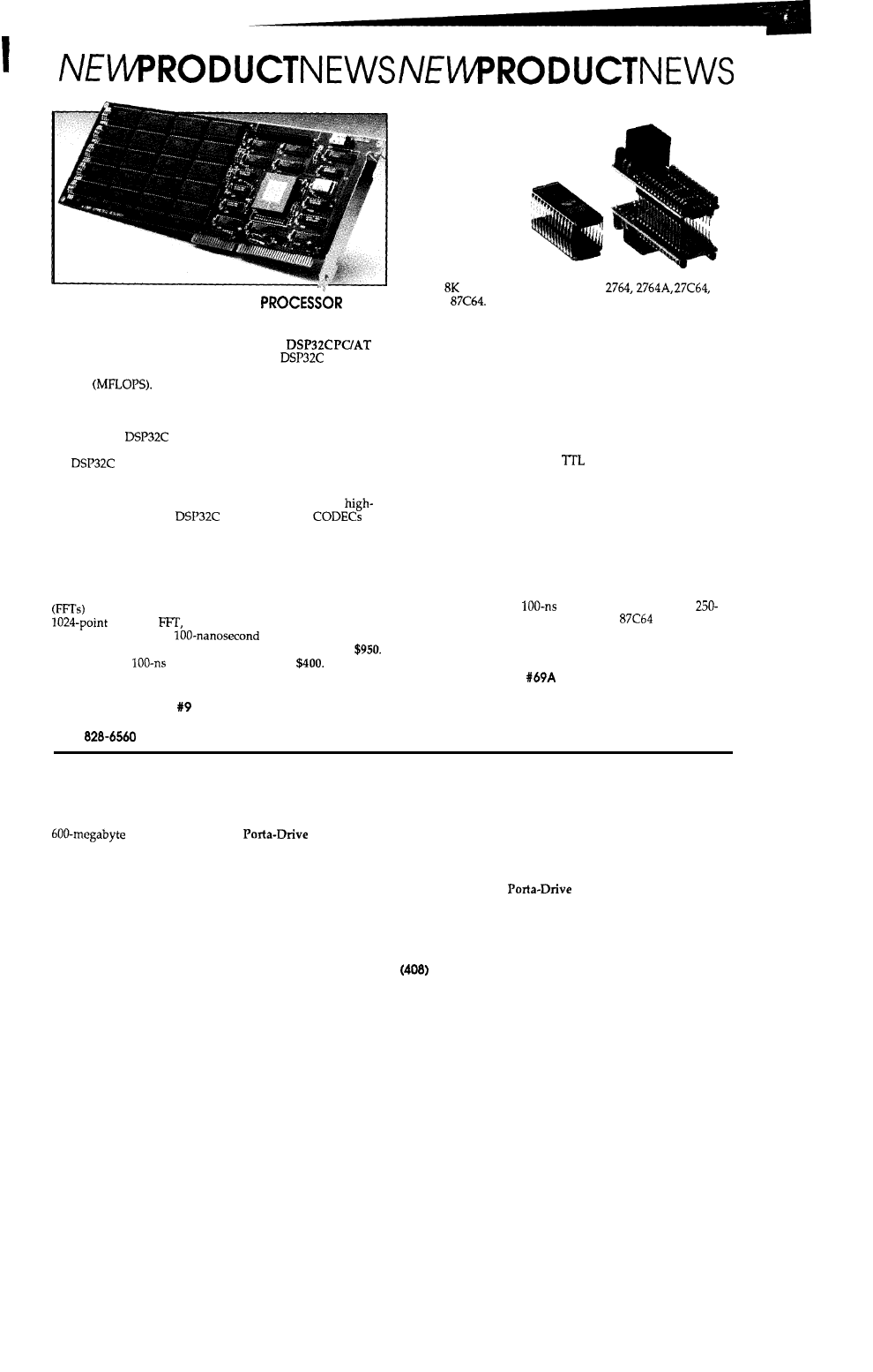
PC/AT DIGITAL SIGNAL
Thirty-two-bit Digital Signal Processing development is
now available with the Symmetric Research
coprocessor board.
The board features the
chip from
AT&T and performs 25 million floating-point operations per
second
It provides state-of-the-art real-time per-
formance for filtering and numerical calculations.
The on-board memory, which is socketed and can be
populated to 640K bytes, is dual ported for simultaneous
access by the
and the PC/AT bus. These features
allow the user to run deep buffers and save them to disk while
the
continues running.
For interfacing to external devices, the board features a
32-bit bidirectional parallel port that can be accessed at full
processor speed. A header provides connections to the
speed serial port of the
for interfacing to
and
other serial acquisition devices.
Software included with the board consists of an assem-
bler, monitor debugger, and math libraries callable from C and
FORTRAN. The source code for all software is included, along
with numerous example programs demonstrating the use of
the board. Fractal computations and Fast Fourier Transforms
are included among the demos. The benchmark for a
complex
including data on and off the board,
is 15 milliseconds with
static RAM chips.
The base coprocessor board including all software is
A full 640K of
memory is an additional
Symmetric Research
15 Central Way, Suite
Kirkland,
WA 98033
(206)
2764 ROM
EMULATOR
A 2764 ROM
Emulator
for use with
the IBM PC and
compatibles has been
introduced by Parallax
Inc. The device
emulates most of the
popular
x 8 EPROMs including the
and Intel
The emulator saves considerable time in de-
veloping ROM code. Instead of being programmed into
EPROMs, software is downloaded to the emulator and run on
the target system within seconds to allow quick code develop-
ment.
Surface-mount technology makes the 2764 ROM Emula-
tor highly reliable and only slightly larger than the 2764 that it
replaces. The emulator accepts SRAM for normal operation,
or EEPROM for nonvolatile use. It connects to the parallel
port of the PC via a modular telephone cable and downloads
8 Kbytes in 2-9 seconds. A tristate reset output restarts the
target system after downloading. HC/HCT logic is used for
compatibility with CMOS and
systems.
The supplied software includes a command-line down-
loader and a full-screen editor. The command-line down-
loader provides a way to download files directly from DOS
and may be called from within batch files for automated
assembly and downloading. For more involved work, the
full-screen editor may be used to edit and download files.
The emulator software accepts Intel Hex, Motorola S, hex, and
binary files, and is written entirely in 8086 assembly language
for quick, dependable operation.
The Parallax 2764 ROM Emulator is available without
memory for $129, with
SRAM for $149, and with
ns EEPROM for $159. An adapter for the
is available
for $49.
Parallax, Inc.
6200 Desimone Lane,
Citrus Heights, CA 95621
(916) 721-8217
PORTABLE CD-ROM DRIVE
The portable office becomes a step closer with CD
Technology’s introduction of a portable CD-ROM drive with a
storage capacity. The
facilitates the
portability of massive amounts of information. It allows
instant access to large databases such as legal and medical
libraries, parts catalogs, and marketing data. With its optional
battery pack, the Porta-Drive can be used anywhere with any
IBM or Apple Macintosh portable computer.
The Porta-Drive, a high-performance CD-ROM drive
manufactured by Toshiba, measures 2” high by 5.8” wide by 9.5
“deep and weighs only 4 pounds. It uses industry-standard
media and cartridges for universal hardware compatibility. Its
total capacity is 683 megabytes with an average access time of
350 ms. The PC and Macintosh software driver allows
compatibility with all CD-ROM products. A SCSI interface
(required if there are no other SCSI devices installed) allows
seven drives to be linked, and they can be stacked to minimize
desktop space. The battery pack offers an estimated computer
time (intermittent access) of 4 hours with a 6-hour charge time.
The price of the
for either the IBM PC or
Apple Macintosh is $895.
The optional battery pack is
$200.
Custom Design Technology, Inc.
780 Montague Expressway, Suite 407
San Jose, CA 95131
432-8698
10
CIRCUIT CELLAR INK
Letters to the
INK Research Staff
VISIBLE
INK
clear and simple
GETTING STARTED WITH THE 803 1
I recently picked up C
IRCUIT
C
ELLAR
INK
and really
enjoyed it. I particularly enjoyed the articles on the
8052 embedded controller and working with LCD dis-
plays. I
working with
I have not yet learned to program in assembly language.
Can you recommend a good starter for the
Jon Williams
Riverside, CA
Thanks fir fhe nice comments about
C
ELLAR
INK.
Weareglad
hopefhaf ifwillconfinuefofuel
your interest in embedded controller design and programming.
There is not the wealth
of
programming tutorials available
for the8052 family
of
microcontrollers
that
for other processors such as the
or the 8086. You
are probably aware
Intel, the
manufacturer of the
8031, publishes the
Embedded Controller Handbook.”
This bookisa referencemanual to the8051 familyand is valuable
information to
have, but necessarily the greafesf for the
beginning programmer. Signefics also publishes the “8051
Microcontroller Users Guide” which some people feel is more
readable
the
version. Signefics is
a second source for
the 8052
products.
fake
a look at the DDT-51 that
was published as a Circuit Cellar project in the Augusf and
September 1988 issues of BYTE.
We
know of one book that describes designing projects
around the 8031 and developing the embedded software to run
them.
Digital Device Control,” ISBN 0-89588-
346-5 by William G. Houghton, is published by Sybex Books.
This book presents a number of examples of how to interface
various devices an 8031 and includes the complete design,
hardwareand software, for a stand-alone EPROM programmer
that
communicates with a hosf computer via an RS-232 serial
port.
COPROCESSOR HELP
Are you aware of any commercially available designs
for a coprocessor board using multiple
or similar
12
CIRCUIT CELLAR INK
coprocessor chips? My particular interest is in a coproces-
sor board for a PC/XT that can be reprogrammed more
easily than
in the Mandelbrot engine and provide
more processing power for numerical calculations.
I am aware of the special coprocessor boards, such as
the Transputer-based boards, but their prices place them
beyond serious consideration. It seems to me that with
some attention to software development, it would be
possible to achieve the same processing power with a
much lower investment in the hardware.
Patrick L.
Jena, LA
We do not know of any commercial boards that use multiple
8087s as parallel numeric processors. One reason for
is
due
to the nature of the way an 8087 works: really is best when it
is tightly coupled to an 8088. You can think of the 8087 as the
silicon that
in the 8086’s case. As such,
you would have to emulate the 8088’s signals and you might as
well use an 8088 rather than go to the added expense of other
hardware.
Actually, while software design is critical to the mission,
hardwareisusuallyfarcheaper thansoftware.
trueacross
just abouf all computer types and sizes. Witness the difference
between the Macintosh
and the IBM PC: The Mac has fewer
chips on the logic board than an IBM PC has on the CGA
graphics
board alone. On the other hand, the software involved
than
You
know which machine is more expensive, right ?
For now, the coprocessor boards you mention are the main
choices for numerical computation. Of course, given the rate of
hardware improvement, today’s supercomputer will beavailable
in just a few years at the local department store.
IRS
201
Very Useful
202 Moderately Useful
203 Not Useful
Building An IBM PC
Keyboard Translator
An 603 7 -based System for Code Translation
V
I admit it. I’m a tag sale
junky. Take me out back and shoot
me, ‘cause I don’t want to be cured.
And to make matters worse, I love
mucking about with micros (as long
as I can get them cheap, of course). So
I have about 12 different systems
hanging around by basement, from
my first system-a hand-wrapped
Altair
alike-to my latest: a
Colony Data Systems
XT clone with
hard drive.
Unfortunately,
these systems have
something in common
besides the (cheap)
price I paid for them.
Every one of them uses
a different keyboard,
with various layouts
and “feels”! ARGHH, I
hate having to remember stuff like
what set of arcane keystrokes is re-
quired to create a control-Q, or whether
the key marked “Del” is really a
or FFH. Lord knows I have bet-
ter things to remember, like what time
the new Star Trek comes on in my area
on Saturday, and did I feed the cat at
all this week? Besides not wanting to
deal with the key differences, I do get
used to a certain touch, regardless of
whether it’s pounding or stroking the
Recently this problem came to a
head when I tried to configure some
word processing software for my
daughter. She has an old Apple II+,
and I was using my Franklin Ace 100
(yes folks, the infamous
to set up
the software for her. After an ex-
tended period spent struggling to
recall what was where on that
blankety-blank keyboard, I gave up in
disgust. I had become addicted to the
IBM-style keyboard attached to my
clone,
typeamatic action, type-
writer feel, function keys, special
numeric pad, and cursor controls.
FEATURE
ARTICLE
Bill Cur/e w
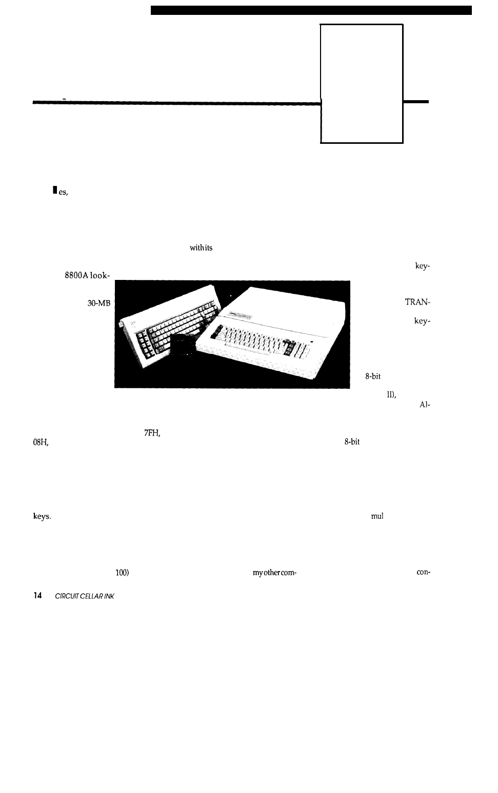
puters, mainly the Apple, Franklin,
and Altair machines. The IBM PC
interface uses a serial-type of data
stream with special keyboard codes,
which I’ll talk more about in a bit. The
Apple and Franklin use an ASCII-en-
coded, parallel-port-attached key-
board, and my Altairs can use either
ASCII parallel or RS-232 serial
boards.
Now to be honest, the Franklin
keyboard on the Ace 100 has a very
nice layout, but the feel isn’t the same,
and it’s kind of dangerous to pull the
thing out of the computer and put it in
your lap. Besides, why should I have
to worry about junk like keyboards in
this wonderful computer age? That’s
when I decided to let a computer solve
the keyboard problem that the multi-
tude of computer keyboard styles had
created in the first place.
. ..AND ONE FOR ALL
I set out to create an interface that
would allow me to use my IBM
PC-style keyboard with
The interface con-
verter presented here,
which I call
SKEY, converts the
encoded IBM
boardcodeoutputinto
ASCII bytes.
The
ASCII bytes can then
be sent to a host com-
puter through either
an
parallel inter-
face (for use with, say,
an Apple an RS-232
serial interface (for use with my
tairs), or both.
Using this converter allows me to
define each key code from the key-
board as an
byte to be presented
to the target computer. Thus, other
character codes besides ASCII could
be supported. A relatively straight-
forward software change would al-
low you to get multiple ASCII codes
from a single IBM key code. An ex-
ample of why you might want this
would be to provide
tiple-byte cur-
sor control sequences.
The TRANSKEY system was de-
veloped on anRTC31 microcontroller,
though anRTC52 may also be used.
The final unit could even be built into
a single 8751 processor with the
trol program and tables in the internal
EPROM.
Note: For mare in-
formation about the
and
see “From the Bench” in issue of
C
ELLAR
INK.1
The combination of serial and
parallel ports available on the 8031
makes it a good choice for this type of
system, but other controllers like the
Zilog Z8 could have been used. In
fact, I got the idea for this project from
some work I had done with the Z8,
using it in another device related to
IBM-style keyboards. The
system
provided key code inputs to the IBM
PC based on input from a slide projec-
tor hand control or an infrared trans-
mitter. The device allowed the nor-
mal keyboard to remain attached and
available at the same time. The re-
search for the Z&based project was
used in the development of the
SKEY system presented here.
THE IBM KEYBOARD
IBM, in its infinite wisdom, has
notone,butatleastthreeuniquekinds
of keyboard interfaces. These change
as you move from PC/XT to PC/AT
to
The main differences be-
tween the keyboard types are the se-
rial data byte format and the way key
codes are identified. TRANSKEY is
designed to work with the PC/XT-
and AT-compatible keyboards which
are most prevalent at (you guessed it)
PC faires and flea markets. These
keyboards use two different signaling
and code identification standards,
known in the IBM lingo as Mode 1 and
Mode 2. Both modes use a special
bidirectional serial interfacecomposed
of a clock line and
a data
line. I will not
be discussing the bidirectional opera-
tion of theinterface in thisarticle, since
it is not implemented by the
SKEY system.
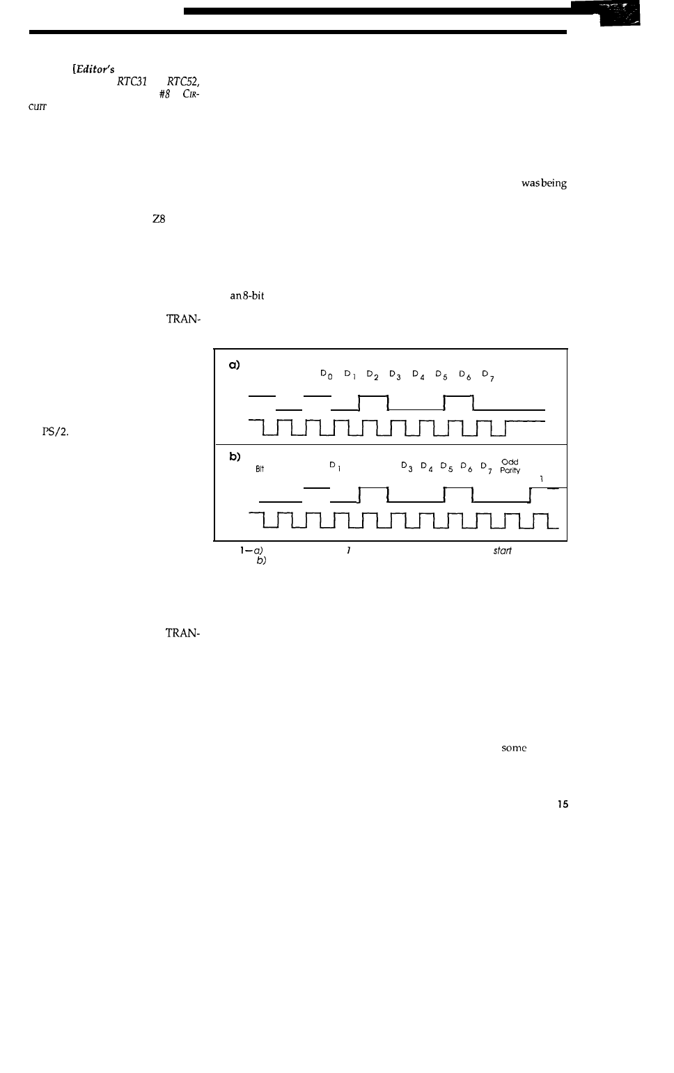
BASIC CODE TRANSMISSION
To transmit a bit, the keyboard
places the appropriate logic level on
its data line, then signals that the data
line should be sampled by moving the
clock line from a logic 1 to a logic 0.
This is very similar in operation to the
way a synchronous modem interface
operates. The data line is valid from
before the falling edge until after the
rising edge of the clock signal.
Bit transmission continues until
all the transmitted bits have been sent
to the processor. The transmission of
individual bits is the same regardless
of the mode in which the keyboard is
operating. Only the number of bits in
a byte and the sequence of codes dif-
fer.
KEYBOARD MODE 1
In a Mode 1 transmission, each
keyboard codeismadeupof ninebits.
The first bit is called the start bit, and
is always a logic 1. Eight data bits
follow. Simple keyboard interfaces
use
serial-in, parallel-out latch
with an overflow line to interface the
keyboard with the computer. The
overflow line on the latch is set to a
Knowing whether a key has been
released is how the shift, control, and
alternate functions are handled. The
receiving system might see the left
shift “make” key code, then the “A”
make and break codes, the “B” make
and break codes, and the “C” make
and break codes. Finally the break
code for the left shift key would come
in. It is up to the receiving system to
remember that the shift key
pressed while the other
key
codescame
in.
Typeamatic action is simply the
transmission of the “make” code over
and over again, and works the same
way in Mode 2.
KEYBOARD MODE 2
Keyboard Mode 2 data transmis-
sion aligns much more closely with an
RS-232-like serial interface’s method
Start
Bit
1
0
1
0
1
0
0
1
0
Data
I
I
I
Clock
Start
Do
D2
stop
0
0
1
0
1
0
0
1
0
0
Data
I
I
Clock
Figure
Key codes in mode keyboard transmissions include a
bit and eight
data bits.
Mode 2 transmission adds a parity bit and stop bit to the end.
logic 1 when the start bit has been
shifted through the latch. At this point,
the eight bits of data are on the latch’s
parallel output lines. The low-to-high
transition of the overflow bit triggers
an interrupt, which causes the com-
puter to read the 8-bit byte, and then
the latch is reset.
The Mode 1 keyboard can trans-
mit a maximum of 128 distinct codes.
Any byte with a value from 0 to 127 is
considered a “make” code (i.e., a key
has just been pressed). Setting the
high-order data bit indicates a ‘break”
code, which means that the key has
been released.
of transmitting bytes, and the make/
break signaling has been changed to
allow for more possible key codes. In
Mode 2, signaling each key code is
done with an ll-bit word, as opposed
to the 9-bit word used in Mode 1. The
timing differences between the two
modes are shown in Figure 1.
Mode 2 transmission begins with
a logic 0 start bit. The start bit is
followed by the eight data bits that
comprise the actual code being sent.
The data bits are followed by an odd
parity bit to provide
level of
data integrity. Last and least comes
the stop bit.
February/March 1990
2764
ROM EMULATOR
Appears as 2764 to
target system.
Connects to
PC parallel port.
Only slightly larger than an actual 2764
Plugs into target ROM socket and connects to PC
parallel port via modular telephone cable
Accepts 8K x 8 SRAM or EEPROM (non-volatile)
restarts target after downloading
Uses
logic for CMOS
compatibility
Loads Intel Hex, Motorola S, hex, and
files
Command line software can be run from botch
files for automatic downloading after assembly
$129
$149
$159
memory,
SRAM)
EPROM
8051
FAMILY ASSEMBLER
l
Works on all 8051 derivatives
l
Supports standard Intel syntax
l
Allows local labels and include files
l
Labels may be up to 32 characters
l
Generates assembly listings
l
Outputs Intel Hex
Quick
l
Dependable
l
Clean Operation
DEVELOPMENTPACKAGE
Programmer 8051 Family Assembler
Programs Signetics
and
micro-
controllers
Handles EPROM, encryption key, and security bits
Loads and saves Intel Hex, ASCII hex, and binary
file formats
Package-DIP
$259
Package PLCC $299
Includes
of PLCC
adapter
PLCC adapter
P A R A L L E L A S C I I
O U T
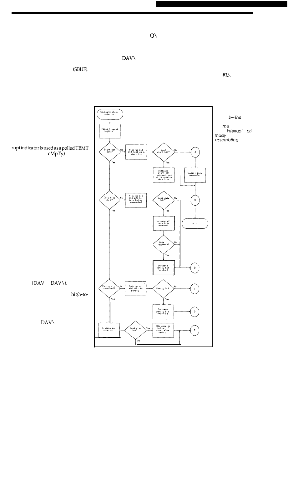
Figure
keyboard
was
I-based microcon-
troller with the additionalinterface hardware shown here. See the article cited in the
which describes the RTC3 for a more complete 803 design.
Another change
in Mode 2 was
the inclusion of a timeout feature on
the AT keyboard interface controller.
The controller starts a timeout clock at
the beginning of each code being re-
ceived. If the entire code is not re-
ceived within 2 ms, the receive opera-
tion is aborted, and an error bit is set in
the keyboard controller’s status word.
THE TRANSKEY SYSTEM
The final difference we care abou t
in Mode 2 deals with how the key code
data is represented to the receiving
system. The high-orderbitisnolonger
used to indicate “make” versus
“break” codes. Instead, a
unique
code,
FOH, indicates the release of a key.
Thus, while make codes can be sent in
one byte, a break code requires two:
the break indicator
and the code
for the key being released.
TRANSKEY performs data
tion, byte translation, and retransmis-
sion. There are three interfaces, one
for the keyboard input, and two for
ASCII output. The ASCII output can
picked up over the serial port, which
is the internal serial register of the
8031 microprocessor, or as an
parallel byte output on port 1. Some
lines from port 3 are used along with
a flip-flop to provide either level- or
pulse-type data-available signals to
the receiving device, and to allow the
8031 to know when it
to transmit
another byte.
KEYBOARD
The use of this coding scheme
Keyboard input is brought into
allows a greater number of keys to be
the 8031 through two bits of port 3, as
supported, and gave IBM an opportu-
shown in Figure 2. The falling edge of
nity to enhance the keyboard interface
the keyboard clock line drives an in-
command set. An example of a key-
board command would be the code
terrupt line in the processor, asking it
to sample the data line. All keyboard
input is handled in an interrupt serv-
at the keyboard. Thiscommand would
ice subroutine, illustrated in Figure 3.
be sent to the keyboard by the AT after
The software keeps track of what stage
BIOS decides how the reception of the
in byte assembly we are in based on
Num Lock key code should affect the
the keyboard mode in use, and en-
LED. Other commands include retry-
forces timeouts and validity checking
ing the last transmission, invoking
keyboard self-tests, and setting the
on the incoming bits. After a valid key
code has been assembled, it is moved
repeat rate for the typeamatic keys.
into a
ring buffer for
R e a d e r S e r v i c e 1 4 4
16
CELLAR INK
ing by the mainline routines. If the
buffer is full at the time a code is
received, the code is discarded.
SERIAL INTERFACE
Serial output of the translated
ASCII codes is accomplished through
the 8031 internal serial register
This register’s output can be sent out
to a bit on port 3, and is taken through
a TTL-to-RS-232 converter IC.
While the serial port has the capa-
bility of running as an interrupt-ori-
ented device, I havechosen to run it in
the polled mode in this system. The
two reasons for that were: it reduces
the complexity of the system software,
and since I require that both interfaces
be clear before sending another byte, I
would end up polling a status indica-
tor somewhere anyway. The TI inter-
(Transmit Buffer
line, which
the main routine checks before at-
tempting to write to the serial output
register.
The speed of the serial transmis-
sion is controlled by an on-board timer.
The initialization routine selects timer
values based on the lower four bits of
the parameter byte passed into the
system at startup time.
PARALLEL INTERFACE
The parallel interface handles
transmission of the S-bit ASCII code
to systems that expect all eight bits at
once. The “port” is really made up of
all of port 1, which is used to output
thedata,and threebitsofport3, which
are used to control handshakingof the
data to the outside world.
An external latch (flip-flop)
is
used
to provide high or low levels of data
available
or
The latch
is driven by three bits of port 3. Port 3
provides a bit which gives a
low pulse when the data at port 1 is
valid for input. The flip-flop changes
state at this point, and provides the
level-oriented data-available lines. In
addition, the
line is brought
back into the 8031, where it is used as
a transmit buffer empty indicator. This
allows the 8031 to wait for the at-
tached computer to acknowledge the
reception of the data before it is over-
written by the next byte.
Because of the way the
line of
the flip-flop is run back into the D
input, the 8031 can reset the flop to a
known state by outputting
one or two
pulses on the
strobe line.
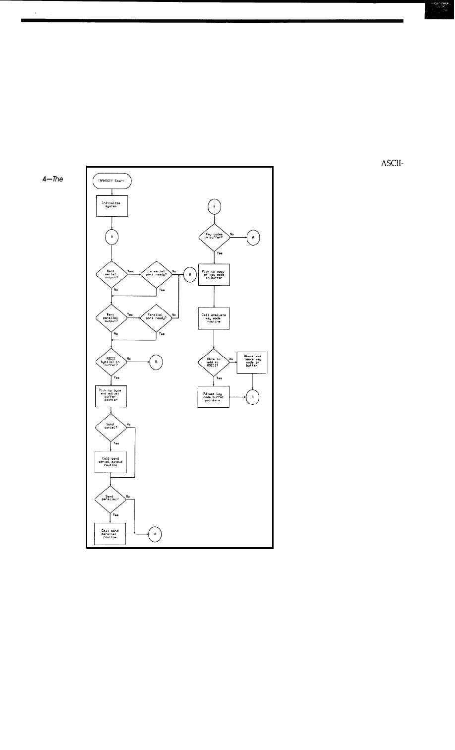
MAIN SOFTWARE ROUTINE
The main driver for the system
has several responsibilities. First, the
serial, parallel, and keyboard inter-
faces are configured and initialized.
At this point, the two buffers used to
hold data (key codes received and
ASCII codes awaiting transmission)
are empty, and the system loops
around looking for work to do. The
major structure of the software is
shown
in Figure 4.
[Editor’s Note:
Software for this article is available for
downloadingfrom the Circuit Cellar BBS,
or on Software On Disk
Seepage 78
for downloading and purchasing infor-
mation.]
Outputting data to the ASCII in-
terfaces is given top priority, which
Figure
inter-
rupt service routine
for
k e y b o a r d
clock
is
responsible for
key
codes as they come
in from the keyboard.
February/March 1990
17
should make the receiving systemvery
happy. One, both, or neither of the
ASCII interfaces may be selected. This
is determined by the bit settings in the
parameter byte passed to the system
at startup time. While selecting nei-
ther of the interfaces may not make
much sense, it is nevertheless pos-
sible.
When the ASCII interfaces
are
idle,
the ASCII code ring buffer is checked
to see if more data is available to be
transmitted. The ASCII interfaces are
always loaded together if both are
selected, and each must wait for the
other to be finished transmitting be-
fore the next byte will be loaded. This
simplifies system design, and will not
usually be a performance problem,
since one of the two interfaces will
normally not be selected.
If either of the selected interfaces
is busy, or there are no ASCII codes in
the ASCII ring buffer, the key code
ring buffer is checked for bytes to be
translated. As mentioned above, the
Figure
main
driver for the key-
board translator is
responsible for initial-
izing the serial, paral-
lel, and keyboard
interfaces, and for
buffer maintenance
and character flow
control.
keyboard routines are interrupt
driven, and are invisible as far as the
main routine is concerned. Data ap-
pears in the key code buffer “under
the covers,“and the main routine only
worries about translating key codes
once they appear.
TRANSLATING KEY CODES TO
ASCII BYTES
There are several things that may
happen when a particular key code is
translated. First, the key code might
be converted directly to an
equivalent code and put in the ASCII
code ring buffer.
Another thing that might happen
is that the key code will cause a status
indicator to be set. Alt, Ctrl, either
Shift key, Caps Lock, and Num Lock
are examples of this kind of activity.
The translator routine must remem-
ber when these
keys are
“made,” since
their settings influence the transla-
tion of the codes that follow.
The final translate option is that
the code will be ignored, which is the
case for most “break-type codes. Ex-
ceptions to this would be the break
codes for either Shift key, Alt, or Ctrl.
TRANSLATION TABLES
While the translator tables and
software are currently set up to do a
one-to-one translation of key codes to
ASCII codes, it would be possible to
set up a one-to-many system. There
are several simple approaches to this
kind of translation problem. One
would be to use translate tables that
had a byte count first, and then the
data to send.
A slightly different approach
would be to use a special code on the
one-to-one table to indicate when mul-
tiple bytes need to be sent. The mul-
tiple byte codes would then be imple-
mented on a different table, using the
tables that have a byte count with
ASCII data following as described
above.
The modified approach would cut
down on the amount of memory
needed for translation, since only the
multiple codes required would be on
the one-to-many table. Most codes
18
CIRCUIT CELLAR INK
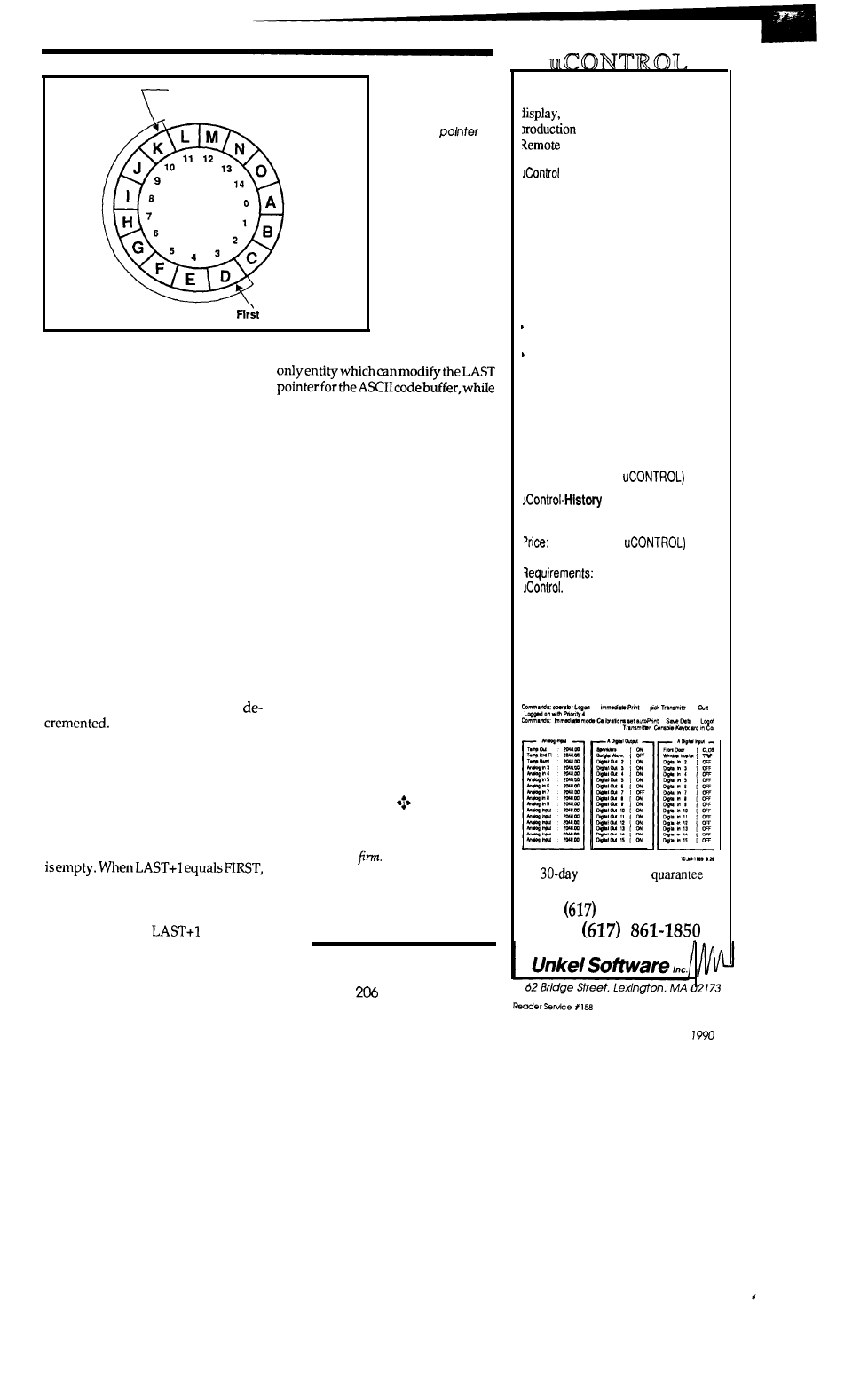
Last or Tail Pointer
“Active”
or Head Pointer
Figure
5-A ring buffer
uses a head pointer
and
a tail
to
keep track of the ac-
tive
entriesin the buffer.
Here, entries D-K are
active.
would be single bytes, and would fall
code buffer. The EVAL routine is the
on the “regular” one-to-one table. This
approach also has the advantage of
being easily implemented on top of
the one-to-one table with little change
MAIN may modify the FIRST pointer
for either buffer.
to the original table or its driver soft-
ware.
THE CAT’S REVENGE
RING BUFFERS
As a final note, I would like to say
a few words about the ring buffers,
such as that shown in Figure 5, used to
hold key codes and ASCII bytes. A
“ring” buffer is one where two point-
ers are used to point into a table of
values. The pointers into the buffer
are called the first and last, or some-
times the head and tail, pointers. In
this system, the buffers are 256 bytes
long, and the pointer values can be
from OOH to FFH. The pointers are
always incremented, and never
Thus, they cycle from 0 to
255 and back around to 0 again, hence
the name “ring” buffer.
If you read the code listing, you
may notice some discrepancies in
coding style along the way. That’s
because this system evolved over the
course of a full year, and was done in
dribs and drabs. Some days I was
partial to the asterisk for comments,
other days it was the semicolon. Sev-
eral PCs were used that all had the
sameprogramdevelopmentsoftware,
but, of course, the tabs were off by a
few columns between them (sigh).
There are two important things to
know about any buffer: When it is
empty and when it is full. This is
easily done with a ring buffer by
comparing the values of the pointers.
When FIRST equals LAST, the buffer
the buffer is full.
As a final note, before I had com-
pleted my tests on this system and its
software, my Franklin keyboard bit
the dust (one bit wouldn’t go high in
the parallel interface). I think the cat
danced on it in revenge for my erratic
feeding schedule. Oh well, anybody
out there know of a good computer
tag sale coming up?
If there is data in the buffer, but
the buffer isn’t full, then LAST won’t
equal FIRST, and
also won’t
equal FIRST.
Bill Curlew is a data processing manager
for a
major
insurance
When not workingwith
mainframe installations, he enjoys developing
microcomputer applimtions and riding mo-
torcycles.
In this system, the interrupt rou-
tine is the only routine allowed to
modify the LAST pointer for the key
IRS
204
Very Useful
205 Moderately Useful
Not Useful
Menu-driven software to monitor,
and control your home or
system on site or from a
location.
Features
Display:
up to 16 analog inputs
up to 32 discrete inputs
up to 32 discrete outputs
Sample Rate:
update all within 1 sec.
Alarms
Switch Discrete Output on:
analog threshold
‘trip’ of discrete line
Password Protection
4 Priorities
MS-Windows based display
customization program.
Price: $175.
Control-Remote ADDS
Dial up from remote to
access all features
Automatic dial-out on
Fault Condition
‘rice: $95. (requires
ADDS
Historical Plotting of any
input or output vs. time.
$95. (requires
IBM PC/XT/AT (compatible)
system with 512k memory; compatible
data acquisition card (inquire about
boards and systems supported.)
Microsoft Windows Release 2.1 or later
required to run configuration program.
-Remote. also Hayes compatible
modems at each end.
money-back
861-0181
FAX
February/March
19
FEATURE
Building
ARTICLE
Part 1
A
Analog-to-Digital Converter for the PC Bus
Conrad Hubert
Dick
he list of applications for flash
is long indeed: Medical instru-
mentation, RADAR, spectrum and
transient analysis, test systems, digi-
tal oscilloscopes,and soon. However,
one drawback to developing a system
which solves one of these “applica-
tion specific” tasks is the loss of gener-
ality inherent in most digital comput-
ers.
*Interleaved 4-KB cache (allows
relaxed memory speed
quirements)
ADC AND POWER SUPPLY
REGULATOR
RAM transfer by
DMA or I/O port read
mode
PC RAM as converted)
*Jumper-selected base address
(allows up to 16 etudes in one
A short time ago, we were in-
volved in a project to build a low-cost
spectrum analyzer for nuclear mag-
netic resonance research, which traded
reduced analog circuit complexity for
increased digital signal processing
burden. One requirement of that in-
strument was an analog-to-digital
section which would accurately quan-
tize signals containing
quencycomponents. From that work,
we learned how to build etude, but
more importantly, we learned that
“application generalized” design al-
lows maximum flexibility in the con-
figuration of both hardware and soft-
ware.
. Jumper-selected
(1 or
output cod-
ing format
l
Turbo Pascal drivers and dem-
onstration software
The heart of the board is TRW’s
hybrid flash converter. The
ADC combines all circuitry required
to convert analog signals into 8-bit
digital data at 25 megasamples per
second. It consists of a wide-band
analog
input amplifier,
age reference, and a
three-state output buffer as well as
zero-scale and full-scale flags.
The hardware design for the con-
verter breaks down into six sections,
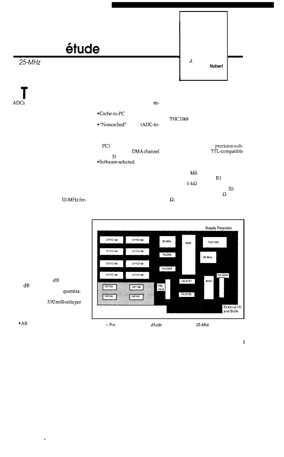
as shown in Figure 1. We’ll take each
section in turn, looking at the compo-
nents and their relationships.
The input impedance of the ADC
itself is 1
A lower impedance
results from installing in parallel
with the
ADC. The closest stan-
dard 1% resistors to terminate
and
75-Q coaxial cables are 52.3 and 80.6
respectively.
Potentiometer R3 allows adjust-
ment of the input offset voltage over a
Cache and Control
Time Base and Multiplexor
ADC and Power
etude is an example of an “appli-
cation generalized” design. Its speci-
fications include:
l
25-MHz maximum sampling
rate
l
lO-MHzfull-powerbandwidth
*Guaranteed 40 SNR (42.5
typical)
l
8-bit resolution (256
tion levels)
*Sensitivity
of
bit
l
Accepts bipolar or unipolar
analog input
Address Generator
r
PC Bus Interface
analog circuitry contained
in a single hybrid package
Figure 1
six major sections of
manage to fit a full
digitizer into an IBM
PC-bus half-length card.
February/March 1990
2
range. This potentiometer is
typically set to provide a l-volt win-
dow centered at 0 volts.
When R3 is set at midpoint, the
ADC will accept bipolar input signals.
As R3 is moved to one extreme, the
input range becomes unipolar posi-
tive, while the opposite extreme al-
lows for unipolar negative inputs.
We recommend adjustment of the
optional gain potentiometer
not
result in more than a 10 percent gain
change. Also, it is more practical to
use R5 solely for gain increases since
this reduces power dissipation in the
Gaindecreases
are better achieved with a resistive
divider at the analog input.
The ADC’s specifications call for
it to withstand voltages between
and -5 volts. Overload protection for
the ADC is accomplished by zener
diodes and D2 which act as clamps
to protect the ADC’s internal ampli-
fier. If the voltage into the BNC is
greater than the zener voltage
volts), they short-circuit the source
driving etude.
is a
voltage regulator
which produces -5.2 VDC from the
PC’s
line. The ECL circuitry
inside the ADC draws about 250
at 25°C. Since a standard PC power
supply is rated to deliver only 300
at -12 V, external power may be sup-
plied via the DB-15 if multiple
are installed in the samecomputer. To
do so, remove jumper W2 and connect
power to pin 9 of the DB-15. The
positive terminal of the supply must
be connected to the BNC common.
This is not necessary in all cases, since
we have drawn over 2000
from a
L
FULL-POWER BANDWIDTH
All Flash Converters are Not Created Equal
We’ll examine how full-power band-
width
applies to
but first a
bit of background.
common type
of ADC is one which uses a successive ap
proximation register
SAR convert-
ers work by first generating a reference
voltage, then using a technique similar to a
binary search algorithm to make increas-
ingly better approximations to the actual
value of the analog signal. They use a
comparator to answer the question, “Is the
input greater than or less than the refer-
ence?”
At the start of the conversion process,
the most-significant bit
in
the
SAR
is
set (turned on). If the reference voltage is
big, the MSB is cleared (turned off). The
process is repeated with the next-most-sig-
nificant bit, and so on down to the
significant bit
This procedure is
valid only if the input remains constant
over the entire conversion. A
holdamplifierisnecessaryforsignalswhich
vary more than 1
during the conver-
sion. An n-bit converter requires, at most,
comparisons.
speed of SAR-based converters
did not meet our requirements, so we se-
lected an ADC called a flash converter.
Flash converters use
comparators
(where is the number of bits of resolu-
tion). They also require a
ladder
network to divide a precision voltage ref-
erence into equally spaced voltages. This
gives the comparators something to com-
pare against. A priority encoder makes an
n-bit binary number out of the compara-
tor outputs. This is all accomplished in
tens of nanoseconds, hence the name
converter. We chose a flash converter for
which, when operating at its maxi-
mum sampling rate, guaranteed its binary
output will accurately reflect the analog
input to within a known SNR specification
rather than aconverter that will simply
not
yield gross inaccuracies at more than some
specific rate.
what are gross inaccuracies?
One of the first applications of flash
to digitize video images in real time.
One-shot from 8253 (also
0
0
0
0
1
1
0
1
0
1
5 MHz
0
External
input
MHz
0
Variable frequency from U23, counter 1
1
10 MHz
0
DMA
1
25 MHz
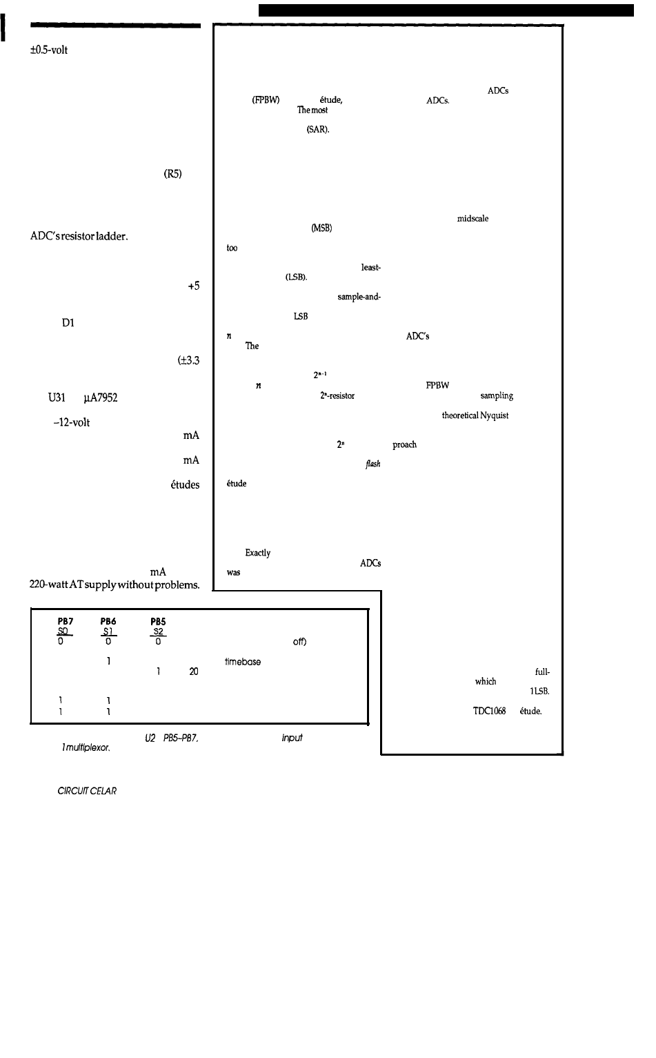
Table
1 -The three ports of I,
select one of eight
sources for the
74LS 15
You may even hear flash
referred to
as video
In NTSC video, the digitiz-
ing rate is just over 14 MHz, so everyone’s
flash converter had to operate at least that
fast. One manufacturer addressed the
question of whether the digitized informa-
tion is always accurate by introducing a
specification which indicated how few
bright-white dots appeared per recon-
structed frame of video information. These
bright-white dots or “sparkles” are due to
spurious codes.
A spurious code is a grossly inaccurate
datum such as a
input signal re-
sulting in a full-scale output code, whereas
a missing code is defined as an output that
has a value less than the lowest possible
quantization level. The bandwidth specifi-
cation for an analog device (in which at-
tenuation is the primary concern) and the
bandwidth specification for a flash ADC
are defined differently. In the latter, FPBW
is derived from the method of testing for
spurious codes, which involves applying a
full-scale sine wave of known frequency to
the
input, and examining the output
for spurious or missing codes. FPBW is
then defined as the
frequency
just
below the
point at which spurious or missing codes
begin to exist.
An
specification of less than
one-half the maximum
rate indi-
cates that performance degrades before
reaching the
limit. This
problem is manifest in wide-band systems
when components of the input signal ap
one-half of the sampling frequency,
while low-frequency multiplexed systems
exhibit degraded performance if the multi-
plexer must switch between adjacent chan-
nels which differ significantly in potential.
Both of these problems are related to the
input signal’s slew rate (the maximum rate
of change of amplitude with time).
The source of these problems becomes
apparent when one realizes that flash con-
verters’ comparators determine all bits in
an output code in parallel by decoding an
intermediate result known as a thermome-
ter code. A thermometer code is a condition
in which a logical one is generated by all
comparators below a specific voltage, and a
logical zero is generated by those compara-
tors above that voltage. If the input signal
slew rate is great enough, there will be more
than one transition from ones to zeros in the
comparator’s outputs, thus causing spuri-
ous or missing codes.
Perhaps a more useful definition of
power bandwidth would establish the
scale input frequency
produced dif-
ferential-linearity errors greater than
Using this definition of power bandwidth,
weselected the TRW
for
It
is capable of full-power Nyquist-frequency
operation at 20 million samples per second.
22
INK
EXTERNAL I/O AND BUFFER
The DB15 connector facilitates
external I/O,
a
trigger buffer cleans up ugly signals.
All signals are
compatible and
run adjacent to a digital ground. The
following are pin assignments and
explanations:
Pin
Output: This is
provided to power external circuitry.
Maximum current draw is not speci-
fied.
Pin
Output: This output
reflects the state of the sample counter.
It goes high when the board begins ac-
quiring data. When the preset num-
ber of data points have been acquired,
the line goes low.
Pin 3-Full-Scale\ Flag Output:
This output is not latched and indi-
cates the status of the sampled analog
data one clock cycle before it appears
as output from the ADC. The
Scale\ flag indicates that the output
bits of the converter are all high. You
may infer a full-scale input only when
true binary output coding has been
selected.
output
latched and indicates the
status of the sampled analog data one
clock cycle before it appears as output
from the ADC. The Zero-Scale flag
indicates that the output bits of the
converter are all low. Again, you may
infer a zero-scale input only when
true binary output coding is selected.
Pin
This
output is the clock signal from which
conversion and storage sequencing is
derived. All of etude’s actions are
listing
1
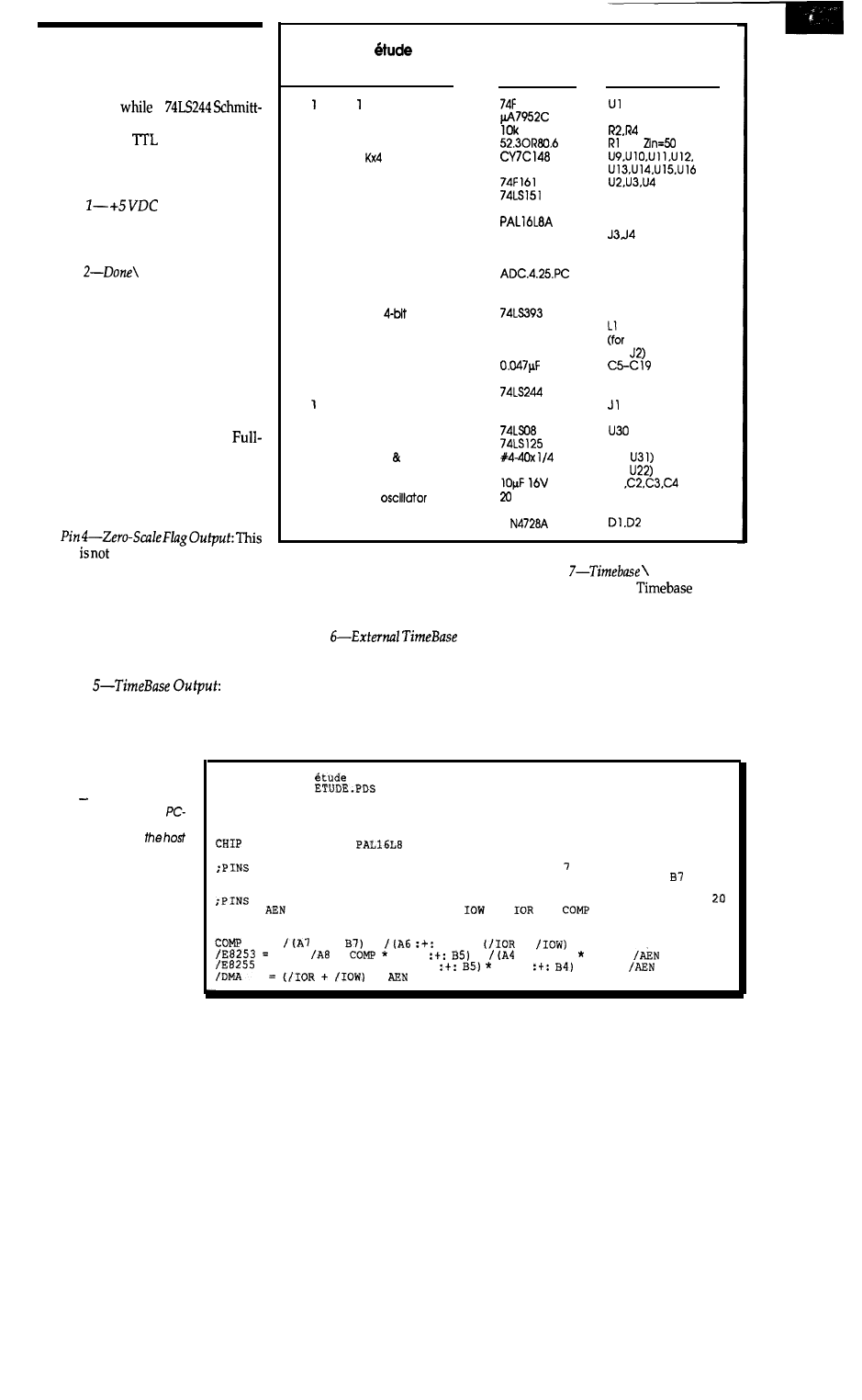
Jhe
PAL equations
are used for decoding
bus l/O space signals during
transferstoandfrom
computer.
Parts list for
Quantify Type
-of-8 decoder
1
-5.2-V regulator
2
0.25-W resistor
1
0.25-W resistor
8
1
SRAM
3
4-bit counter
1
8-to-lmux
1
25-MM 8-bit ADC
1
Address decoder
2
Berg strips
4
Berg jumper
1
Card bracket
1
Circuit board
1
Counter/timer
1
DB-15 female
1
Dual
counter
1
Ferrite on lead
1
insulator mica
2
Jack screw assy
15
Monolithic
1
Multiturn pot
1
Octal buffer
PC-mount BNC
1
PPI
1
Quad 2-input AND
1
Quad buffer
1
Screw nut
1
Socket Augat
4
Tantalum
1
Xtal
1
Xtal oscillator
2
Zener
Value
138
1%
TRW THC 1068
2x3
8253-5
F/R2743009 111
2k
8255
24-pin
MHz
25 MHz
1
Ref. Des.
u31
(for
or 75)
U24
u22
U26
(none)
(none)
PCB
U23
J2
U25
U3 1)
(for
R3
U27
u21
U29
(for
(for
Cl
osc 1
osc2
referenced to the rising edge of this
signal. It reflects the software-selected
acquisitionrateonly when thecacheis
filling; otherwise it is low.
Pin
Input:
This input is selected via software and
becomes the master clock signal for
etude. It may be used to acquire data
at a rate unavailable internally or to
utilize a higher accuracy/stability
clock than the on-board oscillators.
Pin
Output: This is
the same signal as
Output,
only 180 degrees out of phase. It pro-
vides the capability of running two
boards simultaneously on the same
input data. In this way, data can be
acquired by the second board in be-
tween the points collected by the first
board. This doubles the effective
sampling rate when the data is com-
bined.
TITLE
ADDRESS DECODER
PATTERN
REVISION
(PRODUCTION VERSION)
AUTHOR
J. CONRAD HUBERT
DATE
APRIL 7, 1989
ADDRESS-DECODE
1
2
3
4
5
6
8
9
10
A9
A8
A7
A6
A5
B4
B5
B6
GND
11
12
13
14
15
16
17
18
19
E8253 A4
A2
E8255 DMA
vcc
EQUATIONS
=
:t:
*
B6) *
t
A9 *
*
/(A5
*
:t: B4) /A2 *
= A9 * /A8 * COMP * /(A5
/(A4
* A2 *
t
February/March 1990 23
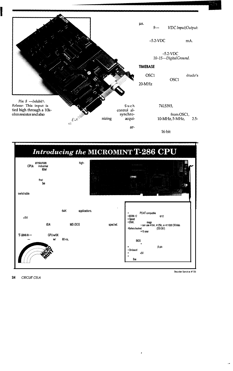
serves
lows
as a hardware trigger. If this
line is pulled low, the ADC
the data
sitionwithextemalevents,
continues to run, but the address
as well as accommodating
generator and sample counter are
bitrary pauses. Efficient use of the
inhibited and data storage is halted.
cache is important
since
2 5 - M H z
operation will fill a 4-KB cache in 163
Pin
-5.2
The direction of this supply is jumper
selected via W2. It is designed to pro-
vide a
output at 50
By
cutting jumper W2, etude’s negative
supply requirement may be provided
by an external
source.
Pins
AND MULTIPLEXOR
and 0SC2 form
internal timebase.
produces a
square wave, while OSC2
produces a 25-MHz square wave.
Another oscillator may be substituted
for 0SC2 to obtain a single sample fre-
quency not available elsewhere.
U25 is a
dual 4-bit ripple
counter. One half of it is unused. The
other half is clocked
so its
outputs are
and
MHz square waves.
U23, an Intel 8253, contains three
independent
counter/timers.
Counter 2 is clocked at 2.5 MHz and
Micromint
the
latest
addition to its line of
quality
for
and OEM applications: The
Micromint T-266. This
PC/AT-compatible computer packs
the features our customers requested most into the single
expansion card formal made popular by the OEM-286. Add the
quality and support
have made Micromint famous, and you
have a CPU that can’t matched for total price, features, and
performance!
The T-266 is 100% AT-compatible, with clock speeds
(via jumpers or keyboard) between 6 and 12 MHz.
Among the features offered on the T-286 are an on-board real-
time clock, socket for an 80287 numeric coprocessor, on-board
keyboard connector, and 4 megabytes of on-board RAM capac-
ity. The T-266 features the industry-standard Award BIOS, and offers OEM customers the
T-286 CPU
Technical Specifications
advantage of a 32K ROM, expandable to
for custom
ISA Bus compatibility is
assured, with the T-266 taking up a single slot in an ISA Bus passive backplane, and requiring
only
power for operation.
Low-power operation; speed; maximum configurability-the T-286 is the perfect choice for
critical applications where
Bus expansion or
software development are
Call Micromint today for more information on the T-266 CPU and custom system availability.
12 MHz 80286
RAM
$ 3 9 9 . 0 0
T-286/4 12 MHz 80286 CPU 4MB
O-wait-state RAM
Call for Prices
MICROMINT, INC.
4 Park Street, Vernon,
CT
06066
Tel: (203) 871-6170 . Fax: (203) 872-2204
100% IBM
processor, operating at
MHz, 0 or 1 wail state
selectable with keyboard or jumpers
1 meg. or 4
of on-bard RAM
real-time clock
and configuration RAM
on-board battery
l
Socket for 80287 Numeric Coprocessor
l
32K ROM, expandable to 64K
l
Award
Configuration and setup routines in ROM
On-board keyboard connector
DIN)
tone beeper
Needs only
for operation
Single-slot, full-length expansion board form-factor
. ISA interface
R
INK
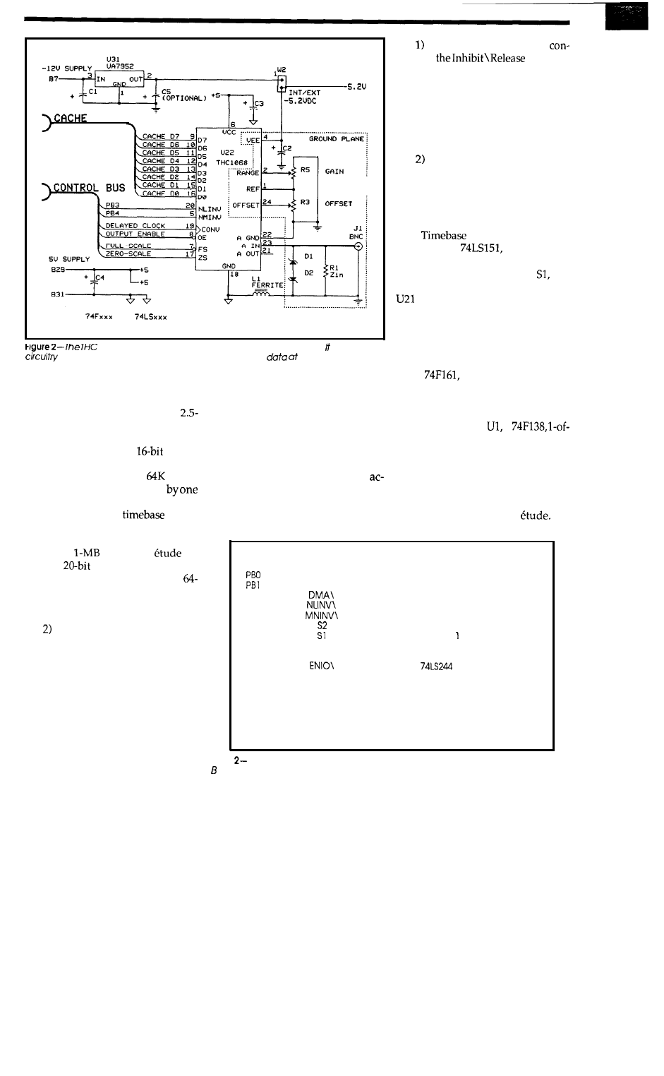
SUPPLY
BUS
( O P T I O N A L
Invert the Done\ flag and
nectit to
line. This
will allow some overrun from the
8253’s preset value. However, the ad-
dress generator will never “wrap
around” and overwrite the first data
points because the terminal count
signal from the
address generator
still
disables the multiplexer.
If no overrun can be tolerated
when partially filling the cache at the
highest sampling rates, a fast external
counter could be employed to gener-
ate an Inhibit\ signal when the preset
number of clock pulses haveemanated
from
Out.
U24 is a
l-of-8 multi-
plexer. One of eight input sources is
selected by a 3-bit input on SO,
and
S2, which is software-generated by
ports PB7, PB6, PB5, according to
Table 1.
ADDRESS GENERATOR
The address generator consists of
three
4-bit synchronous bi-
nary counters U2, U3, and U4. These
chips form a fast 12-bit counter with
look-ahead carry. The circuit is built
in conjunction with
a
8 decoder, which generates cache chip
selects.
PC BUS INTERFACE
We use the PC’s I/O space as one
way to communicate with
It is
SEPARATE UCC FIND GND BUSES
F O R
FIND
C H I P S
7068 hybrid flash converter is the heart of the board.
contains the
needed to convert analog signals into d-bit digital
25 megasamples per
second.
provides the capability to increment
the address generator via a one-shot.
Counter 1 is clocked from the
MHz output of U25. It provides fre-
quencies which can be obtained by
dividing 2.5 MHz by a
binary
integer. (Dividing by two yields 1.25
MHz, while dividing by
yields
approximately 38 Hz. Division
is not possible.) Counter 0 is clocked
from U3 which is the
output
divided by 16. The input to counter 0
is divided by 16 for two reasons:
1) the
version of
re-
quires a
address generator, and
the 8253 counter/ timer has only a
KB range, therefore we must scale the
count by a factor of 16. (1 MB divided
by 64 KB = 16.)
25 MHz is too fast for an 8253 to
count. Since counter 0 receives every
sixteenth clock pulse, this slows the
maximum count rate to 25 MHz di-
vided by 16, or 1.5625 MHz.
Originally, the sample counter
was intended to halt data acquisition
after a preset number of points had
been acquired. Unfortunately, at the
highest sample rates, the 8253’s delay
between reaching terminal count and
its output pin changing states was
long enough to allow the cache to
overfill. Now the terminal count sig-
nal comes directly from the address
generator when the cache is full. Of
course, at slower acquisition rates it is
still possible to poll the 8253 in real
time to determine how much of the
cache is filled, and then halt data
quisitionvia software. If partial filling
of the cache is required at the highest
rates, there are two alternatives:
Port
Reserved
Reserved
PB2
PB3
PB4
PB5
PB6
PB7
so
PC0
PC1
PC2
PC3
PC4
PC5
PC6
PC7
Name
Reserved
CLR
Reserved
INHIBIT\
WR\
RD\
OE\
Function
DMA enable
ADC output coding format
ADC output coding format
MUX control bit 2
MUX control bit
MUX control bit 0
Enable
I/O buffer
Zero address generator
Halt address generator
Cache write
Cache read (not used in 4KB version)
ADC output enable
Table
Control for the chips in the cache section of the design are latched through ports
and C of the 8255, using the individual bits shown here.
February/March 1990 25
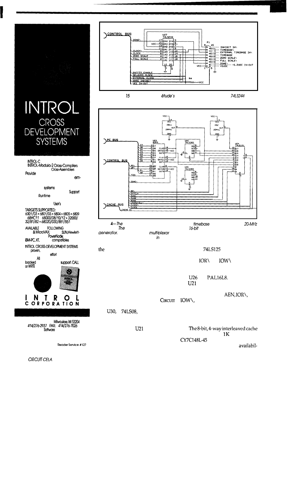
l
Cross-Compilers
l
l
INTROL-Macro
cost and time efficiency in
development and debugging of
bedded microprocessor systems
All compiler
include:
Compiler
l
Cross-assembler
l
utilities
l
library, including
multi-tasking executive
l
Linker
l
One
year maintenance
l
manual, etc.
l
l
FOR
HOSTS
VAX
Apollo;
Packard; Gould
Macintosh;
AT and
are
accepted, and will save
you time. money,
with your devel-
opment. INTROL products are
by full technical
fcf facts NOW:
647 W. Virginia St.,
Quality
Since 1979
Figure
3-A DB- connector is the
link to
the outside world. The
buffers
the incoming and outgoing signals for the entire board.
Figure
basic signal for the digitizer’s internal
is generated by a
oscillator.
8253 provides three independent
counter/timers for the address
lJ24 is a l-of-8
with eight inputs selected by software which
corresponds to the ports shown Table 1.
only
way to program specific para-
meters, like trigger source, acquisi-
tion rate, output coding format, and
so on, and provides a way to read data
from the cache. etude also allows a
faster, albeit more complicated, way
to read large blocks of the cache into
main memory via either DMA
chan-
nel 1 or 3. We will discuss DMA
further in the next issue of
C
ELLAR
INK.
a
is a quad AND
gate. Three-fourths of it are used to
generate conditioned AO, Al, and chip
select signals for
when DMA is
requested. One-fourth is used as an
active-low OR gate for the address
generator hold circuit.
U29 a
is a quad buffer
with enables. One-half of it buffers
the PC’s
and
signals. The
other half is enabled during DMA re-
quest and acknowledge cycles.
is a
Chip selects
for
and U23 are derived by de-
coding the PC’s I/O space signals A9
through A3, AO, Al,
and
according to the equations
shown in Listing 1.
CACHE AND CONTROL
consists of eight x 4 CMOS
Cypress
chips.
We used
these chips because of their
26
R INK
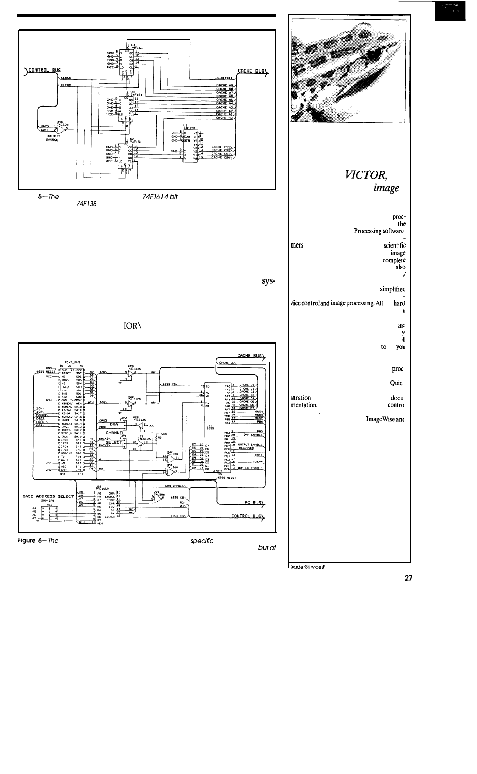
Figure
Address Generator is three
synchronous binary counters in
conjunction with a
l-of-8 decoder.
ity, since they are much faster than
they need to be for this application.
Software-based control tasks are
assigned to U21, an Intel 8255 pro-
grammable peripheral interface oper-
ating in mode 0. It latches control
signals and provides a common port
for both DMA and I/O port access to
the cache. This yields flexibility of op-
eration without any sacrifice in per-
formance. Port A provides bidirec-
tional I/O for cache-to-PC data trans-
fers during both DMA and
cycles. Ports B and C latch control
signals for the other chips. Individual
bits in ports B and C are shown in
Table 2.
CONSTRUCTION TIPS
When integrating a high-per-
formance ADC into an existing
tem,somecompromisesareinevitable.
We would have liked to keep the
analog and digital grounds from the
power supplies separate and used a
single-point ground mecca directly
under the ADC. Unfortunately, that
PC’s I/O space allows for programming of
parameters such as
trigger source, acquisition rate. and output coding format. DMA transfer is faster,
a cost of increased complexity.
Develop powerful
image applications
quickly and easily
Introducing
the
video capture and
processing library
VICTOR, the
video capture and image
essing library, is the latest product from
developersof ZIP Image
Victor is a library of functions for C program
that simplifies development of
imaging, quality control, security, and
database software. Victor gives you
control of your video frame grabber and
includes image processing, display, and TIFF
PCX file handling routines.
Application development is
because we’ve taken care of the details of de
the
low level coding has been done -- and you car
concentrate on your application.
Yoursoftwarecan have features such
live video on VGA, pan and zoom, displa
multiple images with text and graphics, pixe
editing and image processing. And, get
up and running quickly, we’ve included ou
popular Zip Image Processing software fo
rapid testing and prototyping of image
essing and display functions.
Victor supports Microsoft C and
C, and includes over 100 functions, demon
and prototyping software, full
and source code for device
routines.. all for only $195.
Victor and Zip support
other popular video digitizers.
VICTOR LIBRARY $195
includes ZIP image Processing
ZIP Image Processing $79
please specify digitizer
Video frame grabbers are also available.
Call (314) 962-7833 to orde
VISA/MC/COD
CATENARY SYSTEMS
470 BELLEVIEW
ST LOUIS MO 63119
(314)
962-7633
110
February/March 1990
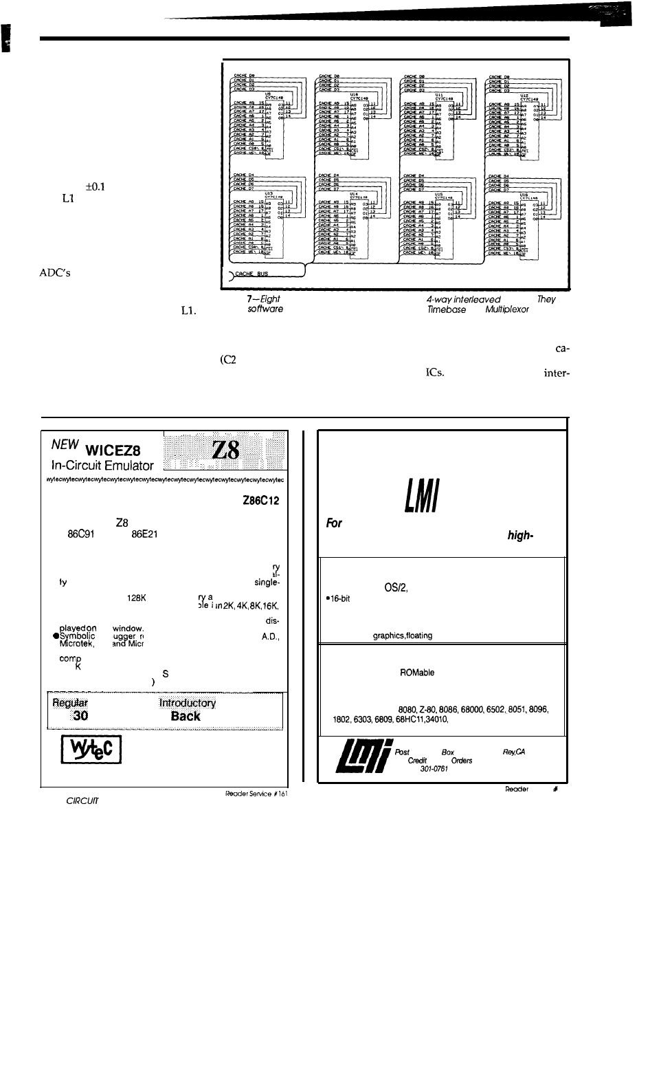
was not
possible
since the PC has a
single common ground for all its sup-
ply voltages. One way to circumvent
this problem is to use an expensive
DC-to-DC converter to produce -5.2
V from the +5-V line. A less elegant
method calls for resistive isolation
between the grounds, but this won’t
help much since TRW specifies that
the analog and digital grounds must
be within
V of one another. We
used as an effective low-frequency
short, yet it attenuates HF switching
noise as its impedance increases with
frequency. It is much cheaper than a
DC-to-DC converter and serves to
keep digital ground noise out of the
analog circuitry. If your appli-
cation can tolerate a somewhat de-
creased SNR, you may find that a
shorting wire works instead of
Perhaps you’ve noticed the use of
aluminum capacitors to replace tanta-
lum. This is because the price of tan-
talum hasincreased dramatically
over
the last few years. Tantalum is still the
choice for high-performance applica-
tions-use it! C5 is not required in the
Figure
CMC148-45 chips provide the b-bit,
cache.
are
under
control of the 8255 shared with the
and
section.
PCB version of the design because C2
and memory chips each get their own
was electrically close enough to U31.
bypass cap. Three other bypass
is intended
to bypass U22.)
pacitors are distributed amongst the
Just as power supply pins are
other
The ADC has its own
implied in digital IC schematics, so
nal bypasses because they are critical
are bypass capacitors. F-series logic
to the operation of that device and
This NEW WICEZ8,
containing the new
CMOS ICE chip, is a complete In-Circuit Emulator
for the entire
microcontroller family, including
the
and the
with 256 internal registers.
l
Comes with window-oriented, user-friendly PC driver
software for the IBM PC, XT, AT or compatibles and permits
real-time emulation up to 20 MHZ.
l
Unique display windows monitor 30 programmable memo
loations or registers, 17 stack locations and are automatica
updated when the user program is stopped or
stepped.
l
Addresses up to
bytes of memo
and external data.
l
Provides 32K emulation RAM mappab e
or 32K blocks.
l
Provides 8 hardware breakpoints which can always be
the
debug er reads symbol files in the 2500
Zax an
Micro Computer Control formats directly.
l
On-line assembler, disassembler, memory/register exam,
are, fill, move, search and modification.
038.4
baud rate for fast upload/download of files in Tektronix
Hex, Intel Hex and Motorola record formats. (Download an
8K hex file in 5 seconds.
Price: $1415
Price; $996
day Money
Guarantee
(708) 894-1440
WYTEC COMPANY
Suite 140, 185C E. Lake Street, Bloomingdale, IL 60108
Total control
with
FORTH”
Programming Professionals:
an expanding family of compatible,
performance compilers for microcomputers
For Development:
Interactive Forth-83 Interpreter/Compilers
for MS-DOS,
and the 80386
and 32-bit implementations
l
Full screen editor and assembler
l
Uses standard operating system files
l
500 page manual written in plain English
. Support for
point, native code generation
For Applications: Forth-83 Metacompiler
l
Unique table-driven multi-pass Forth compiler
l
Compiles compact
or disk-based applications
l
Excellent error handling
. Produces headerless code, compiles from intermediate states,
and performs conditional compilation
l
Cross-compiles to
V25, RTX-2000
l
No license fee or royalty for compiled applications
Laboratory Microsystems Incorporated
Office
10430, Marina de/
90295
Phone
Card
to:
(213) 306-7412
FAX: (213)
Service
28
CELAR INK
external ones simply will not work.
Also, according to good PCB layout
practice, the VCC and GND traces of
the F-series chips are separate from
those of the LS-series chips. (F-series
chips tend to produce more switching
noise than LS-series chips on their
supply leads.)
In general, it is poor practice to
socket high-speed analog circuitry.
The dielectric constant of the plastic
socket is inevitably greater than that
of air and the resulting interelectrode
capacitance can often create problems,
as does moving the IC away from the
ground plane. We have used ma-
chine-tooled sockets for the ADC with
no degradation in performance. This
is due to the
low input imped-
ance and high (3.92
per
sig-
nal levels.
This concludes the hardware out-
line. In the next issue we will examine
the driver software.+
Conrad
Hubert owns Deus Ex
Engineering, a St. Paul,
Minn. consulting
firm and
is a partner in Silicon Alley Inc., a
Seattle-based manufacturer
of
DSP products.
In his spare time he likes to sleep.
Coop, is a partner in Silicon Alley, and has
been involved with microcomputers
for
ten-lo-
the-sixth years.
is
available from:
Inc.
59593
Ren ton, WA
both
and
forms. The kit
contains: board,
4 of SRAM,
manual, and software for $99.00
tested
version
for $495.00.
able
for $5.00.
Extended cache versions
and 1
are
available from
Rapid Systems, Inc.
North 34th
Seattle,
WA
IRS
207 Very Useful
208 Moderately Useful
209 Not Useful
Complete your reference
You cannot afford to miss an issue of Circuit Cellar INK
SOLD OUT
March/April
SOLD OUT
May/June
SOLD OUT
July/August
SOLD OUT
September/October-Issue
November/December-Issue
The above issues are available as a Bound
Reprint of the First
Year of Circuit Cellar INK. Every printing of the Circuit Cellar INK
Bound Reprint Book has been a sellout. Don’t miss out on the current
printing of this popular technical resource! To order your copy of the
First Year of Circuit Cellar INK, send $20.00 ($24.00 foreign
funds only) to:
Circuit Cellar INK First Year Reprint
4 Park Street
l
Vernon, CT 06066
or Call
875-2199 for immediate delivery!
January/February
April/May
June/July
SOLD OUT
August/September
October/November
December ‘89Nanuary
Issue
To order Circuit Cellar INK back issues, send $4.00 check (Visa,
Mastercard accepted) for each issue to:
Circuit Cellar INK
Back Issues Sales
4 Park Street
l
Vernon, CT 06066 or call
875-2199
TM
The DA/M
The Lowest Cost Data Acquisition System
Our DA/M can solve more of your
data
acquisition
problems at a lower price than any other product on the
market. DA/M’s are used for:
l
Military meteorological stations.
l
Building management.
l
Automated hydroponic farming.
l
Industrial process control.
Your application
In
fact, DA/M’s can be used whenever you can’t afford
to use any one else’s product.
Made in North America,
are available NOW!
February/March 1990 29
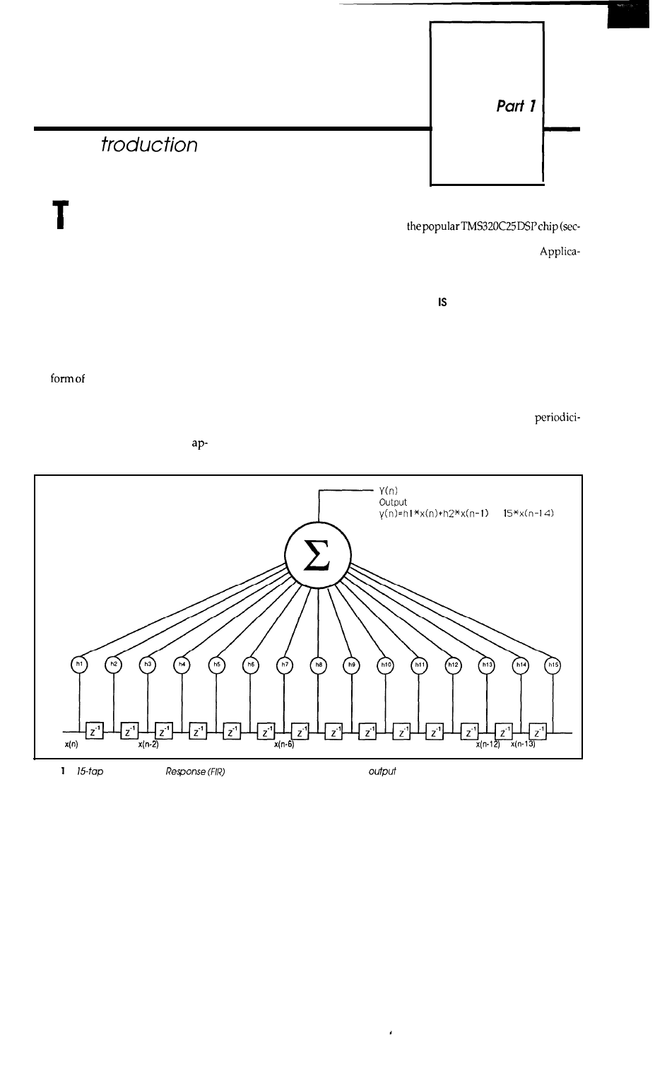
FEATURE
ARTICLE
Digital Signal Processing
-An In
Dean McConnell
he term “Digital Signal Proc-
“microprocessor-like” DSP chips, first
essing” for most individuals conjures
unveiled in 1983, moderately priced
up thoughtsof exotic, complex mathe-
DSP performance is now available.
matics and advanced electrical engi-
Many engineers, technicians, and com-
neering theory. Digital signal proc-
puter programmers with program-
essing, as a specialized field, is rela-
ming and/or circuit design back-
tively new, developed and made
grounds would like to learn about and
popular over the last quarter century
experiment with DSP but don’t have
with the advent of solid-state elec-
access to DSP hardware. Since most
tronics and the integrated circuit.
do own or have access to PCs, graph-
During this period, DSP required
ics-based BASIC language programs
expensive computing equipment in
will be provided in the first part of this
the
mainframes, minicomput-
article which will “visually” demon-
ers, or specialized high-speed DSP
strate various DSP fundamentals. For
hardware.
Until just recently, the
more advanced experiments requir-
specialized hardwarerequired placed
ing high-speed real-time performance,
DSP out of the reach of the serious ex-
“DXP-25” will be offered. DXP-25 is a
perimenter. However, with the
low-cost IBM-compatible PC card and
ond-generation Texas Instruments
Digital Signal Processor).
tionsutilizing the kit will be discussed
in Part 2 of this series.
WHAT DSP?
DSP is formally defined as any
digital operation performed on an
input sequence of numbers. The se-
quence of numbers may range from
stock market data to digitized human
speech. DSP can be applied to stock
price data to find hidden periodicitics
just as it can be used to find
ties (pitch period, formants, and
voiced/unvoiced detection) in human
pearance and subsequent deflation of
support software package based on
speech.
input
..h
x(n-1)
x(n-3)
x(n-4)
x(n-5)
x(n-7)
x(n-8)
x(n-9)
x(n-10)
x(n-11)
x(n-14)
Figure -A
Finite Impulse
digital filter. Each number in the
is equal to the sum of the inputs above it.
30
CIRCUIT CELLAR INK
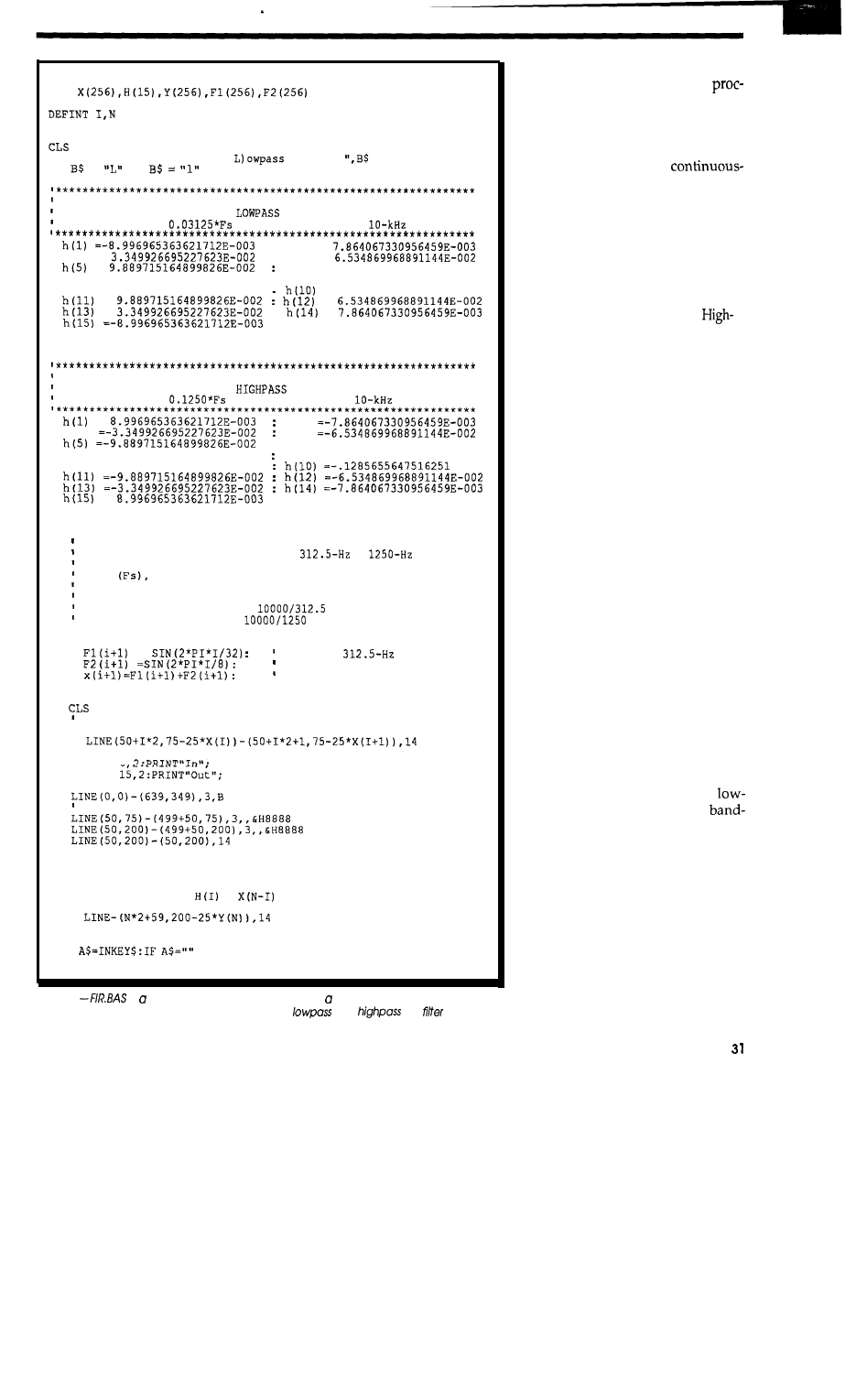
'Finite Impulse Response filter program
DIM
PI = 3.14159265
LENGTH = 15
'number of taps in digital filter
SCREEN 9,0
'IBM XT EGA Mode 640x350 with 16 colors
INPUT" SELECT H)ighpass or
filter:
IF
=
OR
THEN
FINITE IMPULSE RESPONSE FILTER COEFFICIENT5
THESE COEFFICIENTS FORM A
FILTER WHOSE CORNER
FREQUENCY IS AT
(or 312.5 Hz for a
Fs)
:
h(2) =
h(3) =
: h(4) =
=
h(6) = 0.1285655647516251
h(7) = 0.1489759534597397
: h(8) = 0.15625
h(9) = 0.1489759534597397
.
= 0.1285655647516251
=
=
=
:
=
ELSE
FINITE IMPULSE RESPONSE FILTER COEFFICIENTS
THESE COEFFICIENTS FORM A
FILTER WHOSE CORNER
FREQUENCY IS AT
(or 1250 Hz for a
Fs)
=
h(2)
h(3)
h(4)
: h(6) =-0.1285655647516251
h(7) =-0.1489759534597397
h(8) = 0.84375
h(9) =-0.1489759534597397
=
END IF
BUILD WAVEFORM TO FEED INTO FILTER
This waveform will consist of a
+
sine wave.
To provide a series of discrete values at the sampling
rate
which is 10000 Hz for this example, we determine
the number points per cycle associated with each sine wave.
For example,
we know that at 0.5 Fs,
it takes 2 points/cycle.
So, for 312.5 Hz,
we have
or 32 points/cycle,
and at 1250 Hz,
we have
or 8 points/cycle.
FOR i = 0 TO 255
=
generate
signal
generate 1250 Hz signal
mix
the two together
NEXT
PLOT WAVEFORM
FOR I = 1 TO 256
NEXT
LOCATE 6
LOCATE
,
SHOW ZERO VOLTAGE LINE
'PERFORM FIR FILTER FUNCTION
FOR N = 1 TO 256
FOR I = 1 TO LENGTH
Y(N) = Y(N) +
*
NEXT
NEXT
100
THEN 100
STOP
Listing
1
is Turbo BASIC implementation of finite Impulse Response digital
filter. The output of the program illustrates both
and
F/R
operation.
Where analog circuits operate on
continuous signals, digital signal
essingfunctionsoperateonasequence
of numbers. Most readers will be
familiar with the fact that analog sig-
nals (whose formal signal classifica-
tion is continuous-time,
amplitude) require conversion to a
digital representation (discrete-time,
discrete-amplitude classification)
prior to digital signal processing op-
erations taking place. (See “Preparing
Analog Signals for DSP” on page 36).
Classical DSP functions generally
include:
l
Digital Filtering (Lowpass,
pass, Bandpass, Bandstop, and
Multiple Band filters)
l
Discrete Fourier Transforms
(used to determine periodic fre-
quency
content of a signal
frame)
*Signal Modulation (generation of
sinusoidal waveforms),
l
Autocorrelation (used to deter-
mine presence of periodic sig-
nals)
*Cross-correlation (used to deter-
mine presence of a periodic
signal with known characteris-
tics)
THE COMMON FILTER
Digital filtering is probably the
most common DSP application. The
fascinating thing about digital filter-
ing is that it can be accomplished with
a simple”sum-of-products” operation
using current and past input samples
multiplied by coefficients. Equipped
with only delays (which can be ac-
complished by storing samples in
memory locations), multiplications,
and additions, we can perform
pass, highpass, bandpass, and
stop filtering of digitized analog sig-
nals. The values of the coefficients
determine the characteristics of the
filter; that is, whether the filter passes
high frequencies, low frequencies, or
a band of frequencies. The number of
delays (or how many past input
samples we keep in memory) and the
precision of the coefficients used de-
termine the sharpness or performance
of the filter (how quickly the filter rolls
off in the transition band). The Finite
February/March 1990
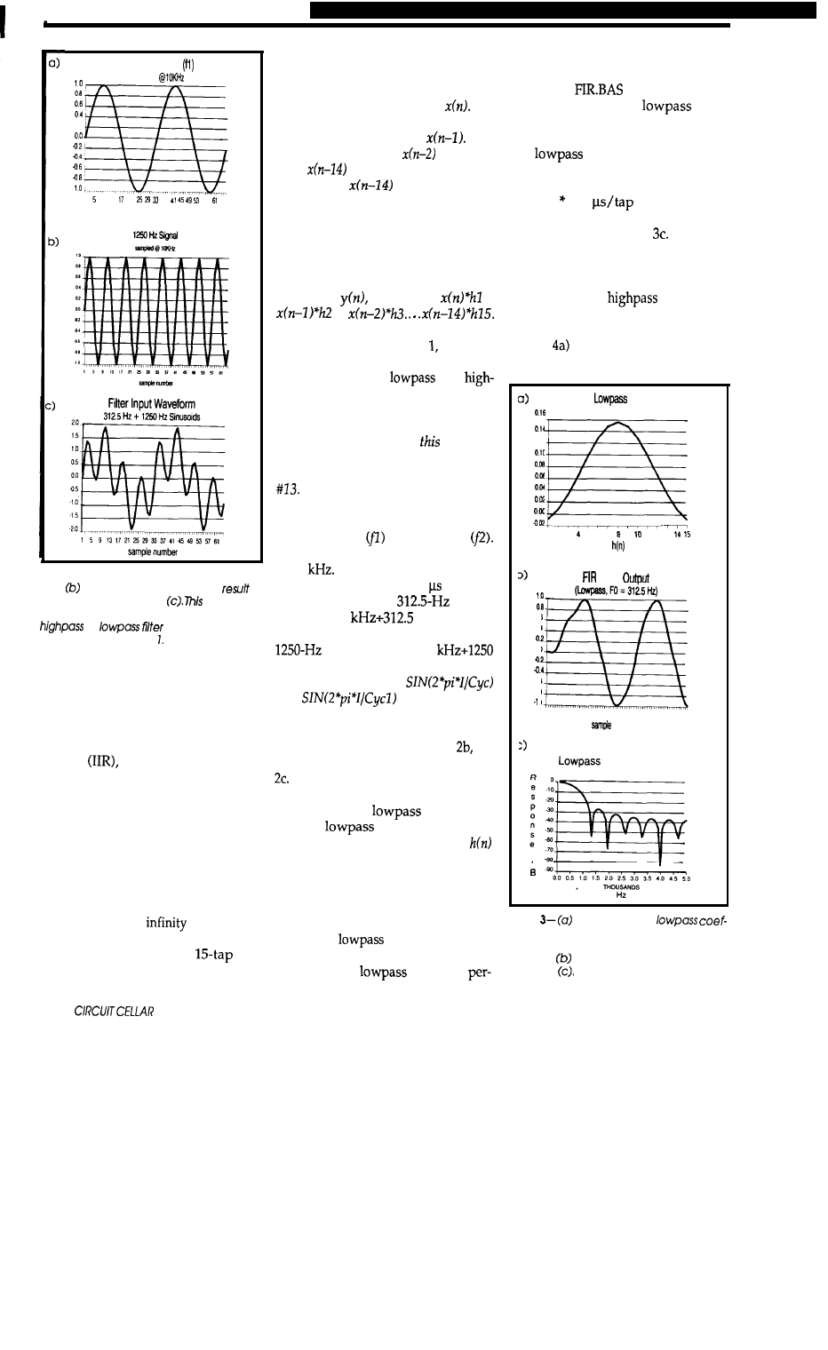
312.5 Hz Signal
sampled
02
1
9 13 21 37 57
sample number
Figure 2-When
the waveforms from (a)
and are added together, the
is
the
waveform shown in
result can
then be further manipulated through a
or
with the charac-
teristics listed in Listing
Impulse Response filter, or FIR, is one
of two major filter types which: uses
only past and current inputs, provides
unconditional stability, and does not
have a counterpart in the analog world.
The other type, Infinite Impulse Re-
sponse
uses past outputs fed
back into the input and sometimes
suffers from instability. An unstable
IIR filter can oscillate just like an un-
stable op-amp circuit. The term “fi-
nite impulse response” means that
after an occurrence of a unit impulse
at the input, the output eventually
settles down to zero. An “infinite
impulseresponse”filtercan,however,
theoretically go to
upon enter-
ing an unstable state.
Figure 1 illustrates a
FIR
digital filter. Input samples enter at
32
INK
the left end of the diagram and move
to the right through each delay ele-
ment as each new sample is ready.
The newest input sample is
The
previous input sample (delayed by
one sample period) is
The
sample before that is
and so on
until
is reached. Input samples
older than
are simply dis-
carded. With each new sample, a
sum-of-products cycle is performed
in which current and past inputs are
multiplied by their respective coeffi-
cients. The summation symbol indi-
cates that each number in the output
sequence
is equal to
+
+
To illustrate the FIR filter operation,
we will introduce Listing FIR.BAS,
a Turbo BASIC program which gra-
phically illustrates
and
pass FIR filter operation. The pro-
gram runs on an IBM PC-compatible
equipped with EGA graphics.
[Edi-
tor’s Note: Software for
article is
available for downloading from the Cir-
cuit Cellar
BBS or on Software On Disk
For downloading and purchasing
information, see page 78.1 The input
waveform consists of two frequen-
cies: 312.5 Hz
and 1250 Hz
Our hypothetical sampling rate will
be 10
This means that each input
sample will be spaced 100 apart. In
order to generate a
signal,
we need 10
Hz = 32 dis-
crete points per cycle. To generate the
signal, we need 10
Hz = 8 points per cycle. Notice that the
denominators in the
and
statements de-
termine the number of points which
define each cycle. Adding the wave-
forms shown in Figures 2a and we
get the composite waveform shown in
To filter out the higher of the two,
leaving only the low frequency (312.5
Hz), we use a
filter. The
desired
characteristics are
determined by the values of the
coefficients. The filter coefficients are
generated using the Fourier Coeffi-
cient method. The resultant values
are shown in the first block of parame-
ters in Listing 1. Figure 3a illustrates a
plot of the
filter coefficients.
Inputting the waveform point by
point into the
filter and
forming a sum-of-products loop, Fig-
ure 3b results. Running a compiled
version of
will demonstrate
the operation of the
filter.
Notice that until at least 15 samples
haveentered the filter, the full effect of
the
filter has not occurred.
The filter is 15 taps long. Therefore,
the output lags the input in phase by
15 taps 100
or 1.5 millisec-
onds. The frequency response of this
filter is shown in Figure By simply
changing the coefficients to those
shown in the second block of parame-
ters in Listing 1, we can do the oppo-
site: construct a
filter.
Performing the same process us-
ing different coefficients (plotted in
Figure gives the results shown in
Figure 4b. The high frequency (1250
FIR
Filter
h(n) Coefficients
012
1 2 3
5 6 7 9
11 12 13
Filter
0.6
0.4
0.0
4.6
4.9
0
I5 913172125292337411549595761
number
d
Filter Response
FO = 312.5 Hz
Figure
is a plot of the
fecients listed in Listing I. When a wave-
form is input and sum of products per-
formed,
results. The filter response is
shown in
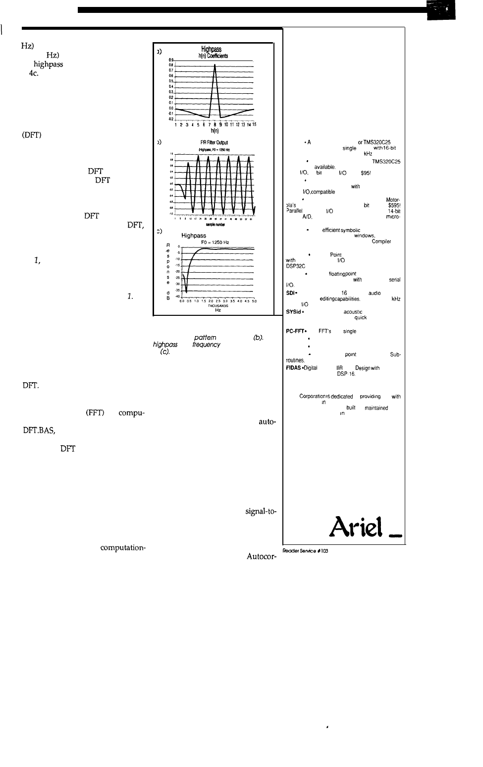
passes while the low frequency
(312.5
is attenuated. Note also,
the
filter frequency response
in
(For a brief explanation of DSP
filter theory, see “How does digital
filtering work?” on page 00.)
A TRIO OF TRANSFORMS
Discrete Fourier Transforms
indicate the frequencies pres-
ent within a frame of data. While the
Fourier Transform operates on con-
tinuous signals (continuous in time
and amplitude), the
operates on
discrete samples. The
algorithm
is a sum-of-products operation where
each sample in the frame is multiplied
by values of a stored sinusoidal wave.
Each point in the
represents a
frequency bin. For a 256-point
we would store 256 points of a sine
wave (from 0 to 360 degrees) in a table.
To evaluate the content of frequency
bin we would multiply each frame
sample by each point in the table. The
resulting sum of products, divided by
256 and then squared, would repre-
sent the power spectrum for
bin To
evaluate bin 2, each frame sample
would be multiplied by every other
value in the table modulo 256. To
evaluate
bin
3, each frame sample
would be multiplied by every third
table value modulo 256 and so on,
until the last
bin
has been evaluated.
One hundred twenty-eight frequency
bins would result from a 256-point
If the sampling frequency were
8,192 samples/second,each
bin would
represent 32-Hz resolution. The Fast
Fourier Transform
is a
tationally efficient version of the DFT.
shown in Listing 2, is a
Turbo BASIC program that demon-
strates the
algorithm. The pro-
gram asks for a relative percentage of
noise which is added to a sine wave
whose frequency is specified in terms
of points/cycle.
You could easily
change the program to accept 512
points of data from a file instead of
generating a noisy sine wave.
CORRELATING SIGNALS
Autocorrelationis a
ally intensive process of multiplying
a
FIR
Filter
Filter Response
Figure 4-Using the coefficients listed in
Listing I
on
the
waveform shown in (a)
results in the
pictured in
lhe
filter
response is shown
in
frame of samples with a shifted rep-
lica of the same frame. As shown in
Figure 5, the duplicated frame is
shifted over one point and multiplied
by the corresponding points in the un-
shifted frame. The sum of products of
each shift formseachpoint in the
correlation output. As an example,
let’s say we’re looking for the pres-
ence of periodic signals buried in noise
yet don’t know anything about the
characteristics of the signal. This is an
ideal job for autocorrelation. A frame
of received signal samples has been
autocorrelated with a duplicated re-
ceived frame as shown in Figure 6.
Notice the improvement in
noise ratio between the original signal
and the autocorrelated output signal.
The spike preceding
the
periodic wave
indicates a large amount of noise
within the received signal.
Digital
Signal
Processing
DSP Development Tools and
Standalone Systems from Ariel
From the IBM PC:
DSP-16
complete TMS32020
De-
velopment System on a
board,
2
channel data acquisition of up to 50
per channel.
PC-C25 The lowest cost full speed
oased card
Just $595 with parallel and
serial
14
analog
IS
just
DSP-56 Integer DSP development system based on
the Motorola 56000 DSP chip
two channel 16 bit
analog
with Ariel’s Bug-56.
PC-56 A new, low-cost DSP card based on
fast DSP56001. Full speed 24 DSP for
and serial
standard. Available with
analog
NeXT compatible DSP port and
phone preamp.
BUG-56 Fast,
debugger for the
PC-56 and DSP-56. Macros,
the works.
Also available: Assembler/Simulator, C
and
TMS320 Code Converter.
DSP-32C Floating
DSP development system
true 16 bit analog
based on AT&T’s 32 bit
chip.
PC-32C Low cost
coprocessor based
on AT&T’s DSP-32C standard
parallel and
A complete, 2 track bit digital
recorder
with advanced
Real-time 50
stereo
using any PC.
Comprehensive
test Instrument.
Developed by Bell Labs for
and accurate
measurements.
Fast
on a
card.
ASM-320 The fastest TMS320 Assembler.
PDS-320 Deluxe TMS320 Program Development,
FFT-320 256 and 1024
TMS320 FFT
Real-time demo program too.
FIR and
Filter
real time
Implementation on the
For You:
Ariel
to
you
the best values high performance DSP products.
Our products are designed,
and
in the
U.S. The best support the Industry
IS
always at
hand. Ariel’s products are sold directly throughout
North America, and are available worldwide, through
our international dealer network.
Ariel Corporation
433 River Road
Highland Park, NJ 08904
Telephone: 201-249-2900
Fax: 201-249-2123
Telex: 4997279 ARIEL
DSP BBS: 201-249-2124
February/March 1990
33
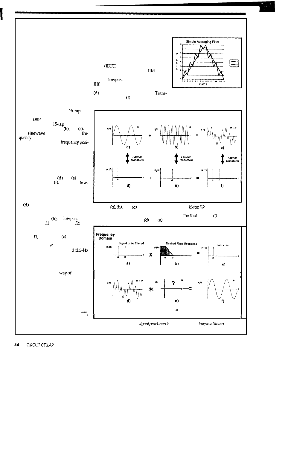
How Does Digital Filtering Work?
In order to provide a very simple
example of a filter function given a set of
noisy data, we can do the following:
Take
a
pair of points, add them together,
divide the sum by two, replace the pair
with the average of the two, and repeat
steps 14 until the end of the data is
reached.
What can be noticed from the dia-
gram shown in Figure I, (which illus-
trates the averaging scheme), is the
smoothing process. The simple averag-
ing technique has, in effect, filtered out
or attenuated the high-frequency noise.
It is fairly easy to understand how this
simple filter works. However, it is not
intuitively obvious how the
FIR
filter works. For this, we will delve into
a little
theory. In Figure II, the
signals used in the
FIR filter ex-
ample are shown in (a),
and
A
pure
is represented in the
domain as a dirac
pulse
(or spike)
placed at theassociated
tion on the x-axis. The vehicle which
allows continuous time domain signals
to be placed in the frequency domain is
the Fourier Transform. To convert fre-
quency domain signals to the time
domain, an Inverse Fourier Transform
is used. Notice, that adding the two fre-
quencies together in
and
yields
the result shown in
In order to
pass filter the composite signal, the fol-
lowing steps can be taken: (refer to Fig-
ure III)
The special coefficients actually represent
a time domain version of the desired filter
frequency response. These coefficients
can be generated through various tech-
niques which include the Fourier Coeffi-
cient and Inverse Discrete Fourier Trans-
form
methods. Convolving the
time domain signal in Figure
by the
waveform shown in Figure 3a yields the
filtered
result shown in Figure
By utilizing convolution, we are able
to leave out the Fourier transform in steps
to (a), and the inverse Fourier
Figure I-A simple filtering technique,
form
in steps(c) to allowing
for efficient
such
as the averaging
scheme shown,
digital filtering.
can effectively
attenuate high-fre-
quency noise.
Time
Domain
Frequency
Domain
1.
convert
the time domain signal
in
to the frequency domain in (a)
2. multiply the frequency domain
signal in (a) by the desired frequency re-
sponse shown in
(a
filter
which
passes
and attenuates
Figure II-
and are frequencies used in the
filter. A sine wave is
shown
as a spike in the frequency domain. Continuous time domain signals are placed
info the frequency
domain via a Fourier Transform.
signal in is the result of
adding the
signals shown in and
3. the result of the frequency do-
main filtering leaves only the lower fre-
quency,
as shown in
4. converting the frequency domain
representation of to the time domain
yields the desired result, the
sine wave.
This approach can be used to per-
form filtering, but is costly in computa-
tion and is not really very feasible. Let’s
lookforamoreefficient
filtering.
We can use
a
Fourier Transform trick
from mathematics which states that
“multiplicationinthefrequencydomain
is equal to convolution in the time do-
main.” This means that by “convolv-
ing” the time domain waveform with a
block of special coefficients, we can
provide an efficient filter implementa-
tion, Notice the special operator,
which indicates convolution. Convolu-
tion is simply a “sum-of-products” op-
eration characteristic of all FIR filters.
Time
Domain
Multiplication in the frequency domain convolution in the time domain...
Figure Ill--The composite
Figure II can be
using the
technique illustrated here, and described in the text.
INK
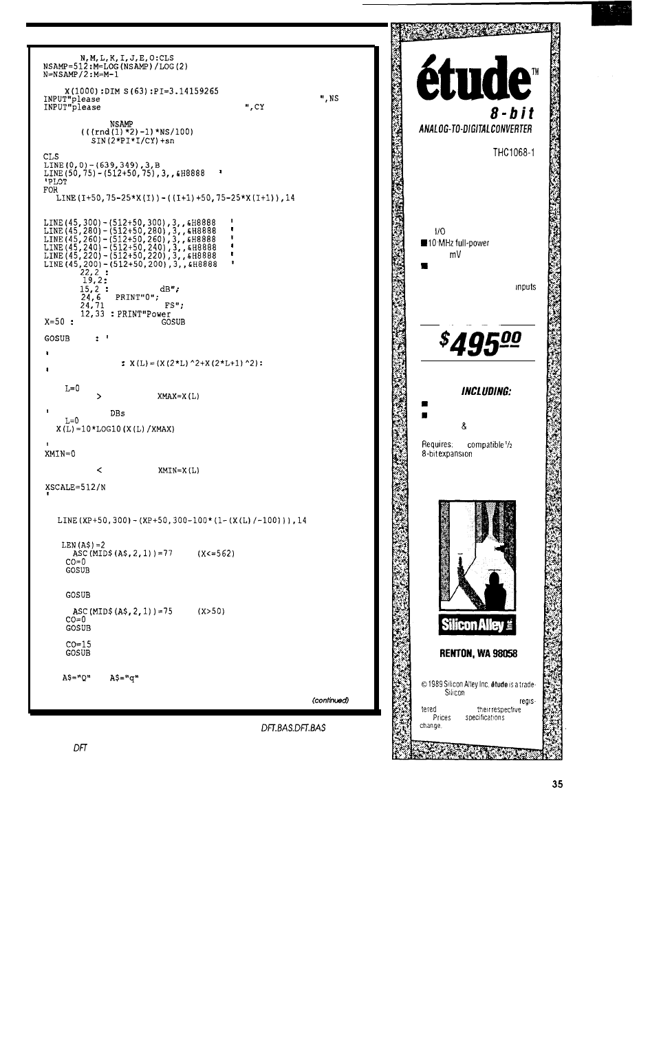
DEFINT
SCREEN 9,0
DIM
enter percent noise to be added to signal
enter points/cycle desired
'BUILD WAVEFORM
FOR I = 0 TO
sn =
X(1) =
NEXT
: SHOW ZERO VOLTAGE LINE
NOISY WAVEFORM
I = 0 TO 512
NEXT
: SHOW -100 DB LINE
: SHOW -80 DB LINE
: SHOW -60 DB LINE
: SHOW -40 DB LINE
: SHOW -20 DB LINE
: SHOW 0 DB LINE
LOCATE
PRINT"-100"'
LOCATE
PRINT"-CO";
LOCATE
PRINT" 0
LOCATE
:
LOCATE
: PRINT".5
LOCATE
Spectrum";
Y-303
: co=15
:
ARROW
FFT
PERFORM FFT FUNCTION
GET MAGNITUDE OF EACH FREQUENCY
FOR L=O TO N-l
NEXT
FIND LARGEST MAGNITUDE
xMAx=o
FOR
TO N-l
IF X(L) XMAX THEN
NEXT
CONVERT TO
FOR
TO N-l
NEXT
FIND SMALLEST VALUE
FOR L=O TO N-l
IF X(L) XMIN THEN
NEXT
PLOT SPECTRUM
FOR L=O TO N-l
XP=L*XSCALE
NEXT
100 A$=INKEY$ : IF A$="" THEN
100
IF
THEN
IF
AND
THEN
ARROW
x=x+2
co=15
ARROW
END IF
IF
AND
THEN
ARROW
x=x-2
ARROW
END IF
END IF
IF
OR
THEN STOP
GOT0 100
STOP
listing 2-A Discrete Fourier
Transform is
implemented in
generates a
sine wave whose frequency is user specified, and adds to it a specified percentage of
noise. The
then works to extract the relevant components of the signal from the noisy
whole.
25 MHz
Based on the
TRW
hybrid flash
converter, its high
signal-to-noise ratio yields ex-
cellent accuracy at the Nyquist
limit.
n
4
KB of cache SRAM or to host
as converted at
DMA
speed
n
or DMA data transfer
bandwidth
n 3.92
resolution
16
jumper selectable base
addresses
n External clock and trigger
TTL compatible
n Software source code included
ALSO AVAILABLE AS A KIT
FOR $99,
Printed Circuit board
Software
n Manual assembly instructions
PC
length
slot DOS 2.11 or
greater. EGA, VGA or Hercules dis-
play needed for graphic representa-
tion of data.
P.O. BOX
59593
206.255.7410
mark of
Alley Inc. Other brand or
product names are trademarks or
trademarks of
hold-
ers
and
subject to
Reader Service X152
February/March 1990
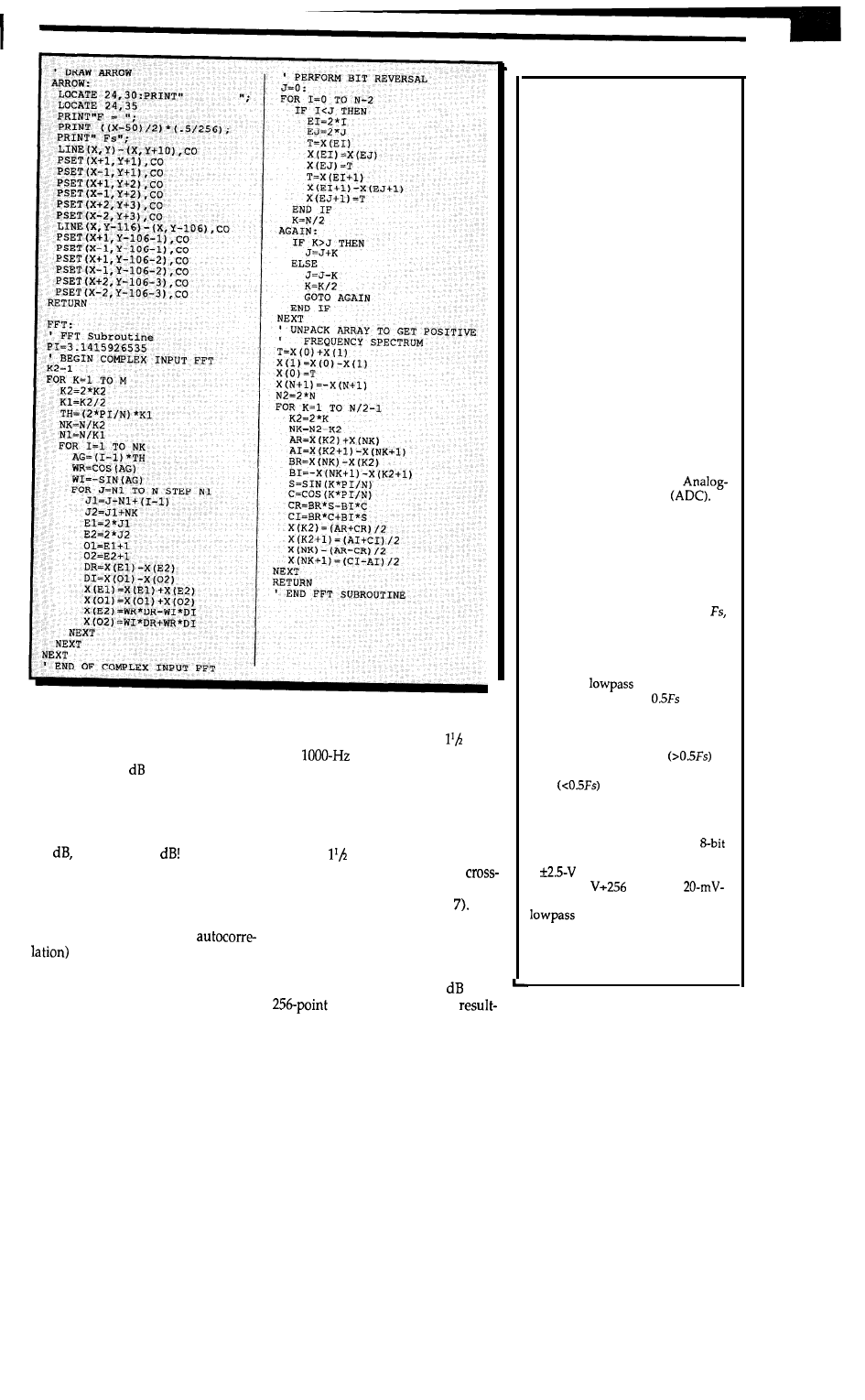
listing 2-continued
relationis a powerful means of detect-
ing periodic signals in noise. If a re-
buried in noise and know beforehand
ceived noisy signal having a signal/
that the signal will consist of cycles
noise ratio of -3 (which means that
of a
sine wave. It is this fact
the noise is twice that of the signal)
that allows us to use cross-correlation
were 256-point autocorrelated with a
rather than autocorrelation. This a
replica of itself, the resulting output
priori knowledge is used to build a
would have a signal-to-noise ratio of
frame of samples which matches the
8.2 a gain of 11.2
characteristics of the signal itself,
Cross-correlation is similar to
namely, cycles of a sine wave at
autocorrelation except that the frame
1000 Hz. The received signal is
of samples is correlated with a differ-
correlated with the known signal
ent frame of samples instead of with
characteristics (see Figure The
itself. It is used (instead of
improvement in signal-to-noise ratio
when the nature of the signal
between the original signal and the
(shape and frequency) is known be-
cross-correlated signal can be signifi-
forehand. For example, let’s say we
cant. If a received noisy signal having
are about to receive a periodic signal
a signal-to-noise ratio of -3 were
cross-correlated, the
Preparing Analog
Signals for DSP
The sequence of numbers (or data)
which DSP algorithms operate on
may originate from daily stock mar-
ket statistics or weekly sales figures
for a consumer product. For con-
tinuous analog signals, however,
which are found in seismic, EKG,
radar, speech, and digital communi-
cations applications (to name a few),
conversion to discrete amplitudes
within specified time intervals is
required prior to proceeding with
DSP operations. The time interval
between each number in a sequence
may be microseconds, milliseconds,
days, weeks, or even years. “Sam-
pling” is the process of converting a
continuous time/continuous ampli-
tude signal into
a
discrete time/dis-
crete amplitude numeric represen-
tation of the signal. The analog sig-
nal is converted to a series of num-
bers through the use of an
to-Digital converter
A
sample-hold circuit (placed in front
of the ADC) “freezes” the input
waveform while theconversion takes
place. At time Tlater, (the reciprocal
of the sampling rate) the process
repeats itself yielding a series of
numbers which represent the ana-
log signal. The sampling rate
must beat least twice the highest fre-
quency component of interest in
order to accurately represent signals
within the bandwidth of interest. In
addition, a
analog filter with
a corner frequency of
must be
placed in front of the sample-hold
circuit in order to defeat the phe-
nomenon of “aliasing.”
Aliasing
allows high frequencies
to
take on the identity of low frequen-
cies
and pass through the
ADC, thus disrupting the DSP sys-
tem. The resolution of the A/D
converter depends on the number of
bits utilized. For example, an
A/D converter capable of handling
a
signal (full scale) would
provide 5
levels or
per-bit resolution. Once the proper
filter, sample-hold, ADC,
and DAC circuits have been de-
signed, DSP operations on analog
signals may take place.
36
CIRCUIT CELLAR INK
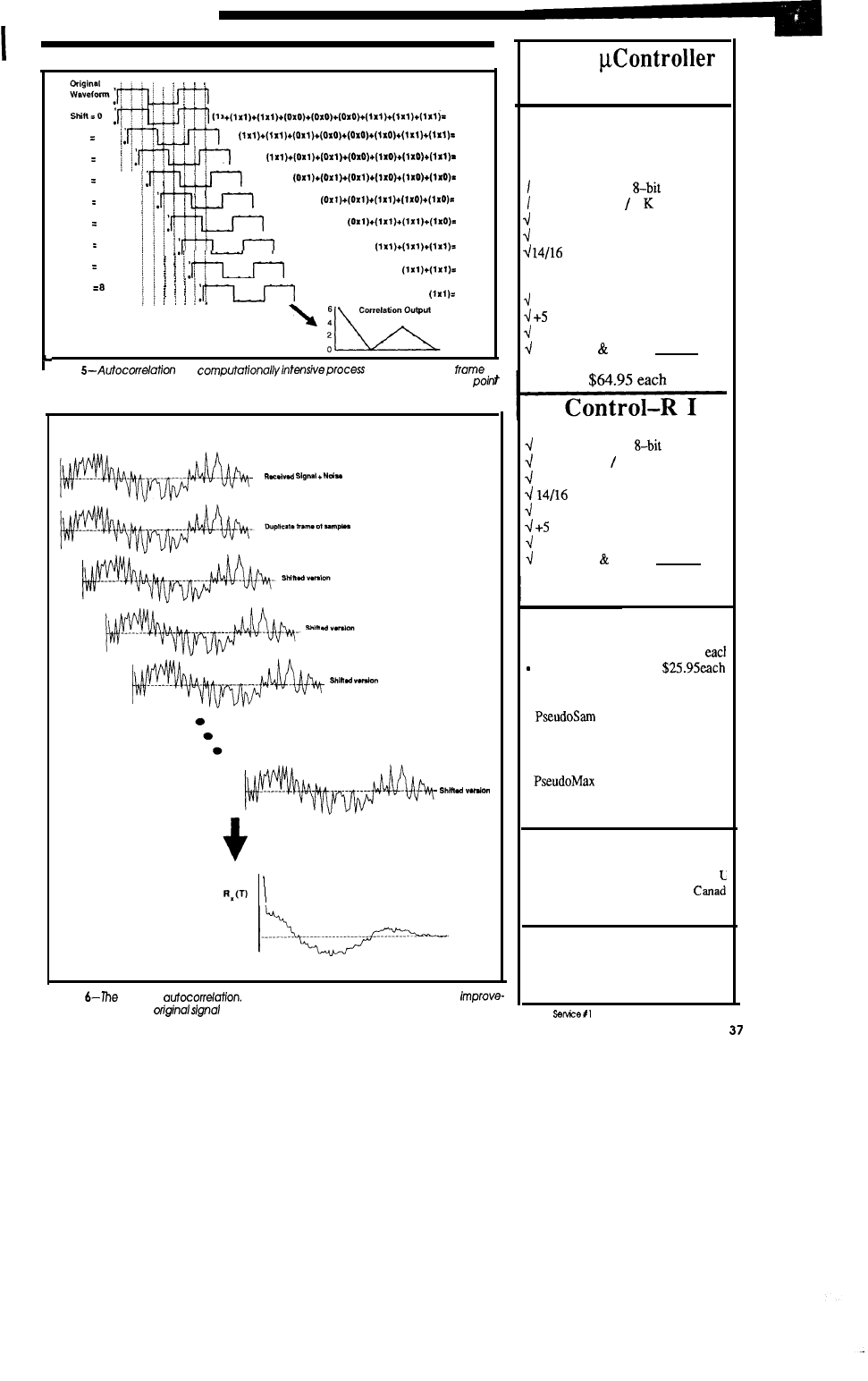
Shift 1
Shift 2
Shift 3
Shift 4
Shift 5
Shift 6
Shift 7
Shift
6
4
2
0
1
2
3
2
1
Correlation Example
Figure
is a
of multiplying a
0
samples by a shifted replica of the same frame. The duplicated frame is shifted one
and multiplied by the corresponding points in the unshifted frame.
f
Autocorrelation
Autocorrelated Output
Figure
result of
The signal-to-noise ratio shows dramatic
ment between the
and the autocorrelated output signal.
8031
Modules
N E W ! ! !
Control-R II
Industry Standard
8031 CPU
128 bytes RAM 8 of EPROM
Socket for 8 Kbytes of Static RAM
11.0592 MHz Operation
bits of parallel I/O plus
access to address, data and control
signals on standard headers.
MAX232 Serial I/O (optional)
volt single supply operation
Compact 3.50” x 4.5” size
Assembled Tested, not a kit
Industry Standard
803 1 CPU
128 RAM 8K EPROM
bytes
11.0592 MHz Operation
bits of I/O
parallel
MAX232 Serial I/O (optional)
volt single supply operation
Compact 2.75” x 4.00” size
Assembled Tested, not a kit
$39.95 each
Options:
l
MAX232 I.C.
$6.95 each
l
6264 8K SRAM
$10.00
8052BASIC CPU
Development Software:
l
51 Software ($50.00)
Level II MSDOS cross-assembler.
Assemble 8031 code with a PC.
.
51 Software ($100.00)
MSDOS cross-simulator. Test and
debug 803 1 code on your PC!
Ordering Information:
Check or Money Orders accepted. All
orders add $3.00 S&H in Continental
or $6.00 for Alaska, Hawaii and
Illinois residents must add 6.25% tax.
Cottage Resources Corporatior
Suite 3-672, 1405 Stevenson Drive
Springfield, Illinois 62703
(217) 529-7679
Reader
14
February/March 1990
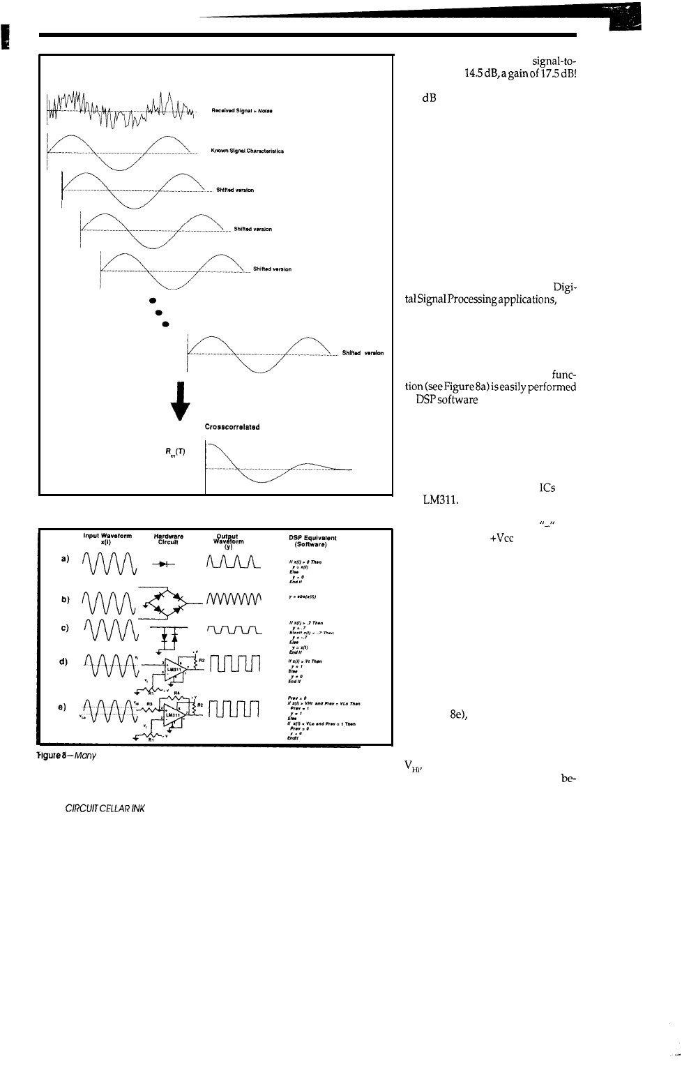
Crosscorrelation
Output
Figure 7 -Cross-correlation offers more dramatic signal-to-noise ratio improvement than
does autocorrelation. but requires prior knowledge of the signal’s
characteristics.
common analog electronic circuits can be successfully replaced by a
DSP chip with appropriate software. Using the DSP approach offers the advantage of
easy on-the-riy
changes when compared with physically changing components.
ing output would have a
noiseratioof
This represents an improvement of
6.3
over autocorrelation.
REPLACING ANALOG CIRCUITS
Although the foundation of DSP
has been built on digital filtering and
spectral analysis, simpler, more mun-
dane functions such as signal rectifi-
cation (digital counterpart of a diode),
threshold excursion detection (analog
comparator circuit counterpart), peak
clipping (digital equivalent of a pair
of diodes connected in a clipping con-
figuration), and signal level measure-
ment (digital counterpart of an RMS
voltmeter) qualify as legitimate
too.
Figure 8 shows a few commonly
used electronic circuits and their DSP
software equivalents. Pseudocode is
used to describe the DSP software
design. A single diode which per-
forms a half-wave rectification
in
as are full-wave recti-
fiers and peak clippers.
As a more in-depth example of
nonclassical DSP, we will look at a
comparator function performed in
DSP software as shown in Figure 8d.
Many of you have probably built
comparator circuits around
like
the
The input signal is ap-
plied to the”+“input while the thresh-
old voltage is applied to the
pin.
The output goes to
as long as the
input voltage exceeds the threshold
voltage. Otherwise, the output goes
to ground or V- (depending on how
you connect pin 1). A variable resistor
allows for changes in the setting of the
threshold voltage. The threshold volt-
age level in a DSP-based comparator
is a variable,
Vt,
instead of a variable
resistor. To change the threshold level,
you change the software statement
which initializes the threshold vari-
able. To add hysteresis to the com-
parator for noise immunity, (as shown
in Figure
the incoming digitized
waveform is first compared to an
upper threshold. After detecting an
excursion above the upper threshold,
the comparator output remains in
the high state until an excursion
38
low a lower limit, V,, occurs. The
output goes low, and the process re-
peats. The range between the upper
and lower threshold levels is the hys-
teresis voltage. This hysteresis pre-
cludes noise excursions within the
window affecting the output transi-
tions. In a DSP approach, the amount
of hysteresis is set by program vari-
ables coupled with program code,
allowing easy changes. The program
HYSTER.BAS shown in Listing 3 is a
Turbo BASIC program which illus-
trates DSP comparator functions (with
and without hysteresis).
Why perform functions in the
digital domain (via
when a di-
ode, comparator, or analog filter
(constructed of resistors, capacitors,
and an op-amp) will suffice? The
answer is flexibility. DSP functions
are typically performed in software
allowing “circuit” characteristics/
transfer functions to be shaped
through program statements instead
of analog components like resistors,
capacitors, diodes, and op-amps
whose characteristics vary with tem-
perature and age. This is analogous to
the early use of general-purpose mi-
croprocessors to replace digital logic
in electronic designs.
DSP IMPLEMENTATION
The previously mentioned BASIC
programs demonstrate DSP funda-
mental concepts, but you may be
wondering how a real application
could be performed. If you equip
yourPCwithanA/Dconverterboard,
you can captureanalogsignals
then perform filtering in
time.
However, if real-time filtering is de-
sired, your PC won’t perform very
well (at least for frequencies
Hz).
In a
real-time PC-based
filtering setup,
the analog signal would be connected
to the A/D converter. The A/D con-
verter would be read through an I/O
port. Filtering would consist of sum-
ming a list of products of coefficients
multiplied by past stored input
samples. The sum-of-products opera-
tion would occur with each new
sample’s arrival. The PC could either
be interrupt driven or could poll the
“end of conversion” pin on the A/D
converter. For a sampling rate of 8000
Hz, (which is required for toll-quality
speech), the sum-of-products opera-
tion must occur every 125 For a
tap filter, the following steps must
occur for each sample:
1. shifteachofthepast 15sample
values down one place in the
storage buffer (drop the old-
est sample)
2. read the current sample from
the A/D converter and place
in the first location of the
sample buffer
3. multiply each current and
past
the 15
(accumulate each
product)
4. output the sum to the D/A
converter
5. wait for the next A/D sample.
On my
IBM PC clone
(equipped with a 286 accelerator
board), it takes approximately 14 ms
to perform the steps outlined above.
SOLUTION
LEARN MULTITASKING
We offer the best quality
SYNTAX FR-4 prototyping PCB at the best price!
All from the stock
. MULTI-BUS
. VME-BUS
. PC-BUS
. PS-BUS
. STD-BUS
.
TRANS
l
Please Call
for Catalog
BOARD
‘Custom Design are Available
l
UNI BOARD
‘Dealer program offered
(818)
Fax:
COLLEGE KIT
The
Kit allows you to learn and to
experiment with multitasking. It includes demo
source code, a tutorial User’s Guide, a
Reference Manual, and
help files everything
you need to try out
The CK is a
reduced version of our
It runs at full speed and is
Use it with MS-DOS or stand-alone. Works with
the 66x86 family and
or Turbo C and
assembler. The full version of
is available
for $1495 with no royalties.
l-800-366-2491
FAX
714-691-2363
CYPRESS, CA
February/March 1990 39
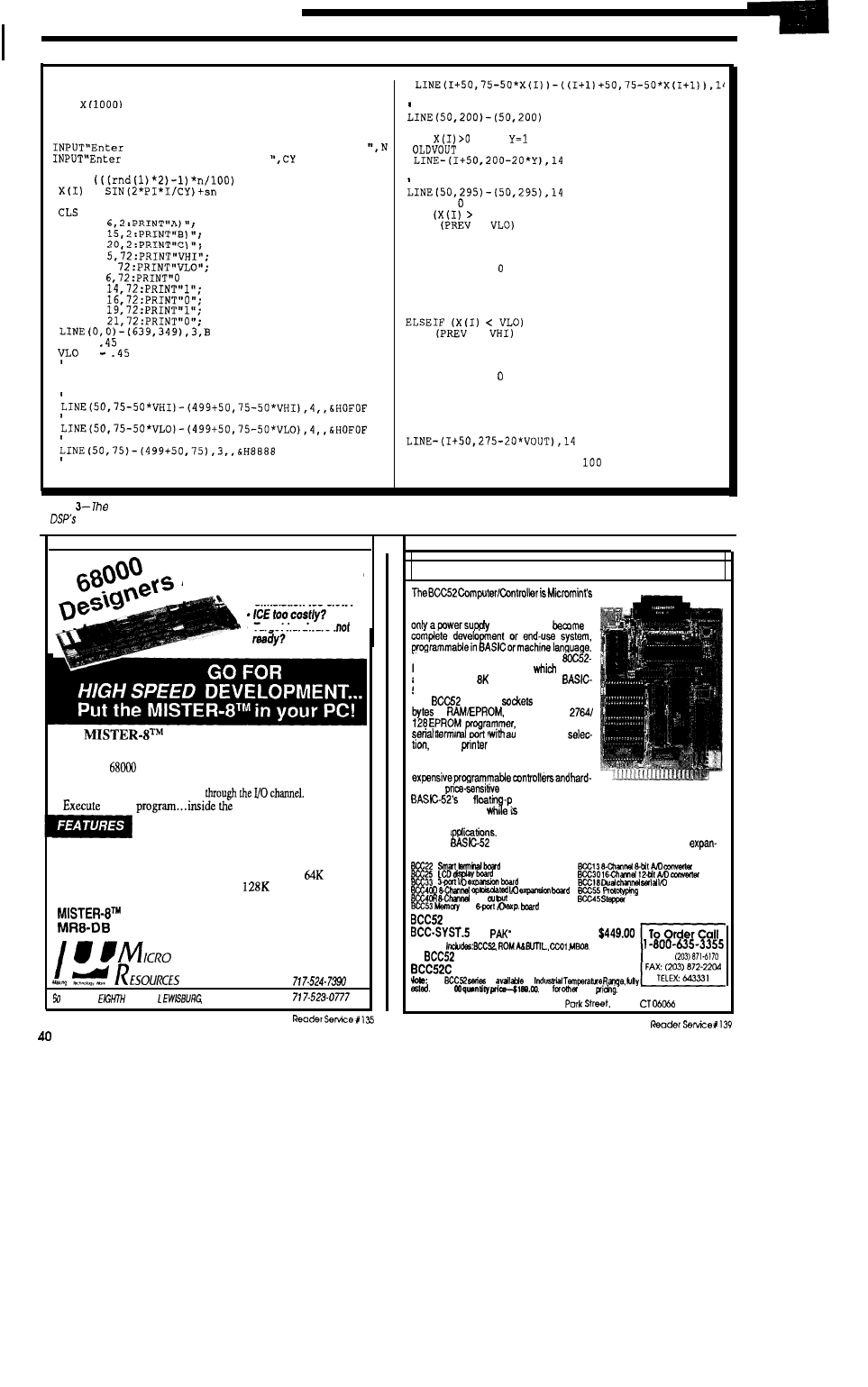
'DEMONSTRATES A COMPARATOR FUNCTION WITH AND
'WITHOUT HYSTERESIS
DIM
PI = j.14159265
DEFINT I
SCREEN 9,0
percent noise to be
added to
signal
points/cycle desired
FOR I = 0 TO 501
sn =
=
NEXT
LOCATE
LOCATE
LOCATE
LOCATE
LOCATE
I,
LOCATE
volts";
LOCATE
LOCATE
LOCATE
LOCATE
VHI =
=
ASSUME OUTPUT INITIALLY OFF
VOUT = -1
PREV = VLO
SHOW UPPER THRESHOLD
SHOW LOWER THRESHOLD
SHOW ZERO VOLTAGE LINE
PLOT NOISY WAVEFORM
FOR I = 0 TO 500
NEXT
DO COMPARATOR FUNCTION WITHOUT HYSTERESIS
FOR I = 0 TO 500
IF
THEN
ELSE Y=-1
= VOUT
NEXT
DO COMPARATOR FUNCTION WITH HYSTERESIS
FOR I = TO 500
IF
VHI) THEN
IF
=
THEN
PREV = VHI
VOUT = 1
ELSE
IF PREV = THEN
VOUT = 1
PREV = VHI
END IF
END IF
THEN
IF
=
T
H
E
N
PREV = VLO
VOUT = -1
ELSE
IF PREV = THEN
VOUT = -1
PREV = VLO
END IF
END IF
END IF
NEXT
100 A$=INKEY$:IF A$="" THEN
STOP
Listing
comparator functions
of
DSP. both with and without hysteresis, are illustrated in HYSTER. BAS. This is another illustration of
a
ability to perform functions normally relegated to the analog electronic world.
ARE YOU FED UP?
.
Simulation too slow?
l
Target hardware
The
is a complete 68000 development
system that can help you get your software out quickly.
l
Write your
program on any
PC/AT or Clone.
*Cross assemble with theincludedsupportsoftware.
l
Downloadathigh speed
l
your
PC.
l
Low cost
l
ACIA allows two-terminal debugging of
complex code
l
Use two or more boards
for multiprocessing
(software support available)
l
Uses
8 MHz 68008,
SRAM; three 28-pin sockets for up to
of your EPROM
code.
with cross assembler . . . . . . . . . . . . . . . $495
Debug EPROM . . . . . . . . . . . . . . . . . . . . . . . . . . . . . . $75
.
or
SOUTH
STREET.
PA
17837
BCC52
BASIC-52 COMPUTER/CONTROLLER
hottest selling stand-alone single-board micro-
computer. Its cost-effective architecture needs
and terminal to
a
The BCC52 uses Micromint’s new
BASIC CMOS microprocessor
contains
a ROM-resident byte floating-point
52 interpreter.
The
contains
for up to 48K
of
an ‘intelligent”
3 parallel ports, a
port
auto baud rate
a serial
port, and it is bus compat-
ible with the full line of BCC-bus expansion
boards. The BCC52 bridges the gap between
to-justify
control applications.
full
-point BASIC is fast and efficient enough for the most
complicated tasks,
cost-effective design allows it to be considered for
many new areas of implementation.
end-use a
It can be used both for development and
Since the
is bus oriented, it supports the following Micromint
sion boards in any of Micromint’s card cages with optional power supplies:
board
relay
board
b a d
a d
Motor bad
BASIC -52 Controller bard
$199.00
‘52
Starter
System
UPS10
OEM 100 Quantity Price $149.00
Tel:
Lower power all-CMOS version $199.00
The
is
h
OEM 1
Cal
OEM
Micromint, Inc.
-4
Vernon.
CIRCUIT CELLAR INK
This translates to a
pling rate of 74 Hz. With a 74-Hz
sampling rate, the highest frequency
that can be described (due to the
Nyquist theorem) is only 37 Hz! If an
80287 numeric coprocessor chip is
installed, the processing time is re-
duced to 1.6 ms, yielding a maximum
sampling frequency of 625 Hz. Even
with a coprocessor, the highest fre-
quency that can be handled is only
312.5 Hz; not very good for real-time
digital filtering of audio signals. We
need a high-speed processor which
possesses special instructions opti-
mized for the sum-of-products
tionsrequiredindigitalfiltering. Gen-
eral-purpose microprocessors like the
80186, 80286, 68000, and so on, lack
this special feature. Custom DSP
plier-accumulator chips and bit-slice
processors are difficult to design and
support even though they provide the
greatest performance. Most high-end,
high-speed DSP
is
performed
through
the use of such circuitry.
An approach which bridges the
gap between general-purpose micro-
processors and exotic bit-slice designs
is the general-purpose Digital Signal
Processor, first unveiled in 1983 by
Texas Instruments (the
Since 1983, many other manufactur-
ers have introduced general-purpose
DSP chips such as the Motorola 56001
(which is used by NeXT), Analog
Devices’ ADSP-2100, and AT&T’s
and DSP32, to name a few.
DSP chip prices have undergone
a dramatic deflation since 1983. For
example, the
(first-genera-
tion DSP chip) originally cost about
$500 in 1983. Now, the same chip
costs around
Future generations
of DSP chips are expected to offer
more performance at lower cost, en-
suring future DSP usage to be wide-
spread. One such chip which cur-
rently offers high performance at
moderate cost is the second-genera-
tion
a 40-MHz CMOS
digital signal processor. By utilizing
this chip with its
instruction
cycle, the
digital filter example
can be performed in only 7
In the next article, we will discuss
the
along with examples
of digital filters and other interesting
applications.
The flexibility of programmable
DSP coupled with the emergence of
low-cost “microprocessor-like” digi-
tal signal processor chips ensures a
“DSP Revolution” in the electronics
world in the 90s just as the micropro-
cessor revolutionized electronics in the
80s.
Dean McConnell is a Senior
Engi-
neer for
Rockwell International, Richardson,
Texas, where he is involved with development
of
real-time computer-controlled communica-
tion systems for military.
receive advance information
about
call or write:
571
Responsive Way
TX
Fax:
548-1521
IRS
2 10
Very
Useful
2
11 Moderately Useful
212 Not Useful
Powerful PC-based Logic Analyzer
for only $595
model for
$745
l
50 MHz Sampling Speed
l
Multi-level triggering
l
8K trace buffer
l
32-channel capability
l
Event Timer/Counter
l
Performance Histograms
l
Hardcopy output
l
Disassembles 8-bit micros
l
and much more
l
Satisfaction Guaranteed
INNOTEC DESIGN, INC.
3304
Cerritos, CA 90703-3304
Tel: 714-527-8540
Accepted
February/March 1990
4
1
The BCCH 16
Porting a Multitasking
to the 76
om
introduced the
microprocessor in
C
ELLAR
INK
His treatment covered the
hardware details of the CPU and the
specifics of this implementation of the
BCCH16 single-board computer.
Hardware is not complete without
companion software; this article ad-
dresses the
of the coin: the
software.
Those of you familiar with the
bit architectures will be pleasantly
surprised by the flexible instruction
set offered by the H16. Like the 68000
family, registers are essentially
less-you can use any register in any
instruction. A wide variety of ad-
dressing modes makes getting to data
easy. Built-in instructions take care of
tedious functions like multiplication
and division. In short, programming
the
is much like working on a
largemainframecomputer,withmany
of the same low-level resources (with
the exception of hardware floating
point>.
The press is full of stories of the
legal firefight between Motorola and
Hitachi, but thisbattlerevolvesaround
the processor and not the H16. It
appears that the H16 is safe from liti-
gation (or, at least as safe as any chip
is in the Silicon Valley tort wars).
REGISTERS
The H16 includes of very fast
RAM that comprises the processor’s
register set. As Tom’s article pointed
out, the RAM can be divided into
memory and a set of 16 32-bit regis-
ters, or as 16 banks of registers, each
bank including 16 registers. I have no
intention of duplicating his particu-
larly lucid description of the various
modes of this memory. I do think that
for most purposes the RAM will be
used completely for registers. The
processor is entirely too powerful for
much help from a little fast on-board
RAM; most applications will use huge
external RAM arrays.
At any time you have access to
registers RO to R15, but with one in-
struction you can change between 16
different sets of RO to R15. Years ago,
as a novice assembly programmer my
credo was “More registers!” Now,
after fixing hundreds of thousands of
lines of old code, I think too many
registers is more a curse than a bless-
ing, since it is usually impossible to re-
member what is supposed to be in
each. Two hundred fifty-six 32-bit
registers is a lot! However, Hitachi’s
banked approach, where only one set
is available at a time, is well suited for
multitasking applications. Although
no sane programmer would attempt
to use all of them in in-line code, if you
allocate one bank to each independent
task (assumingno more than 16 tasks),
then a context switch can occur in
about a microsecond. More on this
later.
So, for all practical purposes the
H16 has 16 general purposes regis-
ters. Its orthogonal instruction set lets
you use any register in any instruc-
tion; where in the HD64180, only the
HL register pair can address memory,
in the H16 any register can. The arti-
ficial restrictions imposed by the lim-
ited number of HD64180 opcode bits
are nonexistent in the H16.
As Tom mentioned, the H16
While
32-bit registers make handling large
Part 2
Jack
integers much easier, they are essen-
tial for providing convenient access to
this large memory space. Any register
can contain all or part of an argument
address; you never have to worry
about not being able to fit an address
into a register.
ADDRESSING MODES
A large part of the power of the
H16 derives from its wide variety of
addressingmodes. Anycomputerlets
you load a register from a specific
address; the more sophisticated per-
mit indirect loads (e.g., load from the
address in register or even double
indirect (e.g., load from theaddress in
the one pointed to by register
The
H16 supports almost every conceiv-
able addressing scheme. Table 1
summarizes each of the legal address-
ing modes.
Some of the modes are identical to
those
you’d
find in any computer. For
example,
Direct
you load from or to any register.
Immediate is just like immediate mode
on the
it lets you load a
register (or memory address) with data
that is included with the instruction
(like
LD HL, 12
3 4). The register indi-
rect mode is used to access a memory
location whose address is in a register,
somewhat like the
LD
A,
except that any register can
hold the memory address.
Other addressing modes parallel
those found in the 68000 family.
Autoincrement and autodecrement
are two of the most useful. The
instruction
MOV
R2 loads R2
with the data in the memory address
pointed to by
is then
42
CELLAR INK
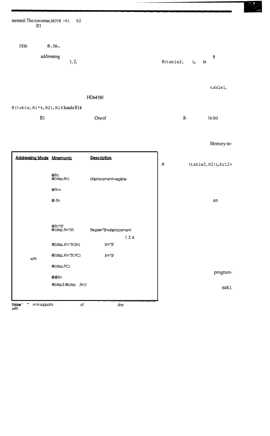
,
decrements before the move. In
handling arrays, lists, queues, or vir-
tually any data structure, these for-
mats are invaluable. As we’ll see later,
the
supports
and 32-bit
transfers; these autoincrement and
autodecrement
modes will
adjust the register contents by
or
4 as needed, so regardless of data type
after the instruction, the register will
point to the correct next entry in your
table. Automatically.
The Register Indirect with Index
and Register Indirect with Scale ac-
cess memory using a number of para-
meters.
As an example, MOV
fromanentryinanarraycalled “table.”
The address in is multiplied by the
scale factor 4 (letting you easily get to
variably
sized
data), and is then added
to the beginning address of the array
(“table”) and the contents of register
R2. Wow!
As with most modem computers, to the final address. You can thus
several Program Counter relative ad- easily work with tables of pointers
dressing modes are included. These without cumbersome intermediate
are formatted much like the other ad- loads. Even better, several displace-
dressing modes. By making the PC ments can be combined so the ad-
one part of the address, it is possible to
dressing register can be independent
write reentrant code--code whose of the table’s base address. A con-
location can be changed without reas- struct of the form MOV (tablel,
sembling the source. This is crucial in
R2)
R3 perfectly le-
complex applications where programs gal and rather mind boggling. R2 is
or overlays are dynamically loaded in added to table2 to form a pointer to
different sections of memory. The memory. This memory pointer is
same program might be loaded at loaded to a internal (nonvisible) regis-
several different locations, so must be ter and is then added to
fi-
address independent.
While the nally yielding the address of the argu-
supports relative addresses ment. Iguessyoumightusethisifyou
with short jumps, in the H16 it is pos- are referencing a table of pointers
sible to code all program transfersand indirectly through another table of
data moves as relative.
pointers.
themoreinterestingmodes
is Register Double Indirect. While
Register Indirect accesses a location
pointed to by a register, Double Indi-
rect uses the contents of a register as a
pointer to a memory-resident pointer
Unlike and many
micro-
computers, you are free to use any
addressing mode with any instruc-
tion. Even better, instructions that re-
quire two arguments let you use any
mode for any argument.
memory moves, without intermedi-
ate register loads, are quick and easy.
Complex constructs like MOV
(tablel, @
are perfectly legal.
Register Direct
Register Indirect
Register Indirect
with autoincr.
Register Indirect
with autodecr.
Immediate
Absolute address
Register Indirect
with scale
Register Indirect
with Index
Program Counter
Relative
index
Program Counter
Relative
Register double
indirect
Rn
register contents
register points to argument in memory
points to
argument
Get argument from memory pointed
to by register; then increment Rn
Decrement Rn: then get argument
from memory pointed to by Rn
#number
Argument Is the number
@number
Argument is at address <number>
Register times Sf points to memory
points to
mem
Note that Sf can be
or 8
Register
+ Rn + disp
points to memory
Register
+ disp + PC
points to memory
Program counter + disp points to
memory
Register Rn points to address of
1
argument in memory
Rn + disp 1 points to memory
value; this value is then added to
disp2 and the result points to the
final argument
I
-me
a large
number addressing modes.
mode may be used
any instruction, and for instructions that use two arguments, any addressing mode
may be used for any argument,
This flexibility does not come free.
More complex addressing modes
require longer opcodes. Obviously, a
memory-to-memory move with the
two addresses specified as 32-bit ab-
solute addresses requires B-byte
opcode just to store the addresses of
the two arguments; additional byte(s)
are needed to specify the instruction.
Further, these lengthy instructions
tend to be slow, since the processor
has many bytes to read before begin-
ning the operation.
Smart programming can drasti-
cally speed these operations and re-
duce code sizes. In fact, specifying a
32-bit address is not something that
has to be done frequently. An index
register can be used to indicate the
start of a data area. Or,
counter-relative addressing might be
used, especially if the data is relatively
close to the code (say, within
Certainly all array and table access
should be made indirectly through a
register, so only the initial load of the
register will require a long instruc-
tion.
February/March 1990 43
PC Bus
Data Acquisition
and Control Cards
STOP
paying a small fortune for
PC data acquisition and control
interfaces!
AD1000
Real
Devices, Inc. designs and manufactures
the lowest cost
interface cards
for the
bus. Our commitment is to offer
only high quality U.S. designed and manufactured
interfaces-not cheap imports.
cards are
backed by a one year warranty, 30 day NO
RISK
return policy,
and free technical
support!
AD1000 8 channel
20
A/D; sample
hold; three
timer/counter; 24
digital
lines.
$295
4 channel
125
three
timer/counter; resistor configurable gains;
24 digital
lines.
$259
AD500
8 channel
integrating
pro-
grammable gain of
1, 10,
Extremely stable
accurate
$239
Single channel, differential input,
integrating A/D;
D/A output; gains of 1,
10, 100. Plus 10 digital
lines.
$215.
channel
25
single
D/A; 24
digital
lines.
$239
Fast settling dual/quad
in-
ternal double buffering.
line
compatible
digital I/O cards; 10 MHz.
Optional
buffers and pull-ups.
$951274
TC24 Five 5 MHz timer/counters; uses power-
ful AM9513 chip. Also 24 digital lines.
$218
FREE
CATALOG
today for your copy of the latest
catalog
and price list for our complete line of
PC
bus data
control, prototyping, ex-
tender cards, technical books and accessories!
Custom/OEM designs on request!
Real Time Devices, Inc.
D
r
.
College, PA 16664
8
The H16 is thus a harbinger of one
programming philosophy of the 90s:
while complex
facilitate easier
coding, they demand more expertise
and more careful analysis of the prob-
lem. Thoughtless use of
programmingconventionswillcripple
the
performance; only by tak-
ing advantage of the inherent struc-
ture implicit in any programming
problems will its potential be fully
realized.
INSTRUCTION SET
Early microprocessors and mini-
computers relied on the “single accu-
mulator” instruction format, where
most memory transactions and all
arithmetic occurred through a single
register (A in the
In the
H16, the instruction set is orthogonal;
every register can address memory,
and each can perform math and logic
operations. Where in the HD64180
careful attention is paid to how regis-
ters are loaded, since math can only
take place on A, in the H16 you can
even do math directly to memory.
of the processor’s registers are
32 bits long, suggesting that 32-bit
math and logic operations are the
norm. This would be quite awkward
when trying to manipulatea character
string! Nearly every H16 instruction
takes several forms, so you can spec-
ify the length of the operation. Want
to move a byte of memory? Issue
MOV. B
A word (16 bits)?
. W
.
course, a long
bit) operation is possible, using the
form
MOV. L
(Note that the
mnemonics use an argument format
reversed from the HD64180. The first
argument is the source, the second is
the destination.)
This word length option is crucial
to any real application, but I feel it
does make the code a bit hard to read.
The 68000 suffers from this problem
as well.
Hitachi publishes several
written and comprehensive H16 data
books, so I’ll make no attempt to detail
all of the instructions here. Rather, I’ll
just describe some of those more com-
monly used.
The move
instruction has
already been informally introduced.
In its various forms it transfers data
between registers, memory, and
with few restrictions.
ARITHMETIC AND LOGICAL
INSTRUCTIONS
operate on registers or memory.
Therefore,
ADD
can work between
registers or memory, as shown in List-
ing 1.
The H16 includes all normal math
instructions, including
SUB, AND, ADD
with carry, decimal add, negate,
NOT
,
logical inclusive and exclusive
OR,
and
compare. Instructions are provided
to perform sign extensions and simi-
lar functions. All of these are pretty
traditional and hold few surprises.
Like other high-performance
processors, the H16 has built-in
ger
multiply and
divide routines. Both
signed and unsigned versionsof these
instructions are provided.
One of the weaknesses of the
HD64180 is its limited multiply in-
struction. The H16 includes both an
16-bit result),
and a 16-by
version yielding32
bits. Normal integer math is therefore
trivial to implement.
The divides are similar. Two
bit numbers can be divided, giving an
quotient and an
remainder.
You can also divide a 32-bit number
by one of 16 bits, generating a l&bit
quotient and a 16-bit remainder.
BIT INSTRUCTIONS
A
number of intriguing bit ma-
nipulation instructions are included.
ADD
;
ADD
a d d r e s s
= data + what
p o i n t e d t o b y
8-bit add
of two memory locations
listing
1
-Any t-i
16
instruction can operate on either registers or memory.
CELLAR INK
A bit field extract
operation
lets you remove any number of bits,
starting at any bit position, in a long
word. Theresultingbitsare
justified in the result and zero-filled to
the left. Tedious rotates and
can
be replaced with a single instruction.
Its complement is bit field insert
In addition, bit test and set
instructions allow you to emulate the
similar
functions.
Six types of shift operations are
provided. The rotate instructions let
you revolve bits around a register to
the left or right, either through the
carry or not. Arithmetic shifts shift a
register left or right, without chang-
ing the sign of the value (i.e., a nega-
tive value will stay negative since the
sign bit will be propagated during the
shift). Logical shifts are similar, but
are
and do not preserve the
argument’s sign. With all of these in-
structions you provide an argument
that specifies the number of bit posi-
tions to shift; the days of multiple
single-bit rotate instructions are hap-
pily long gone.
PROGRAM TRANSFER INSTRUCTIONS
The
offers a number of pro-
gram transfer instructions. Both un-
conditional branches and jumps are
included; the branch instruction is
always PC relative.
JMP
can take any
addressing mode, so you can even do
a double indirect through memory
pointers.
Similarly, the branch to subrou-
tine
instruction is program
counter relative while jump to sub-
routine
can use any addressing
mode. The subroutine invocation in-
structions all save the return address
on the stack, inviting the use of the
RTS
(return from subroutine) instruc-
tion.
Like many computers, the
maintains a condition code register
that tracks the results of the previous
instruction. While most nonarithmetic
instructions don’t affect the condition
codes, the move instructions do, sig-
naling an important departure from
the HD64180 family. Beware when
converting code!
Conditional branches are crucial
to loop control and decision making.
The H16 has a good selection of these,
covering conditions such as carry set
or clear, zero or
greater than,
less than, minus or plus, or overflow/
nonoverflow. All branch instructions
are program counter relative, pro-
moting the use of reentrant code.
Unlike most 8-bit
whose rela-
tive conditional jumps are usually
limited to fairly short jumps (typically
bytes), the H16 supports both
short and word
displacement)
jumps.
MISCELLANEOUS INSTRUCTIONS
One powerful instruction pair is
LDM
(load multiple registers) and
STM
(store multiple registers). These take
a
indicating which reg-
isters to save or restore, and a memory
arraydestinationaddress.
They could
beusedforconvenientcontext switch-
ing (although I prefer switching regis-
ter banks if no more than 16 processes
are competing). Other applications
The ideal solution for embedded control
applications and stand-alone development.
l
8052AH BASIC
CPU
l
Serial printer output and 5,
8
bit
ports
l
5
area
l
Memory:
RAM, expandable to 128K
Power requirements:
300 ma. only
l
PROM
for 2764 or 27128 EPROM
l
Interrupt handling capability
l
Built to exacting standards and warranteed
l
Still only $228.00 including documentation (quantity
far
the
now! 603-469-3232
q
Binary Technology, Inc.
Main Street PO
67
NH 03770
PC-based emulator for
SEE
n
PC plug-in or RS-232 box.
Pages D
1324-1326
n Pull-down menus with
full window support, combined with
commanddriven User Interface.
n
Up to 3.3 MHz (E clock) real time emulation.
n
No intrusions to the
resources.
48 bit wide 16K deep trace. All functions usable without
disturbing emulation. Time stamping. Two level trigger.
n
Symbolic and C Source Level Debugging, including in-line
assembler and disassembler.
Prices: 64K Emulator and pod $2590: 4K Trace
CALL OR WRITE FOR FREE DEMO D/SK!
E. Campbell Avenue
Campbell CA 95008
FAX
376-7869
C O R P O R A T I O N
(408) 866-1820
‘US
February/March 1990
include debuggers, short interrupt
service routines, and the like.
“String” instructionsareprovided
to support automatic looping. They
permit block moves (like the LDIR
instruction in the
and com-
parisons.
create stack frames, as used by
many compilers and some assembly
programs.
LINK
pushes a register on
the stack, saves the SP to the register,
and then adds an immediate value to
the SP.
UNLK
reverses this process.
These instructions provide a conven-
ient way of passing parameters on the
stack-a common activity in C.
HD64180 C compilers really suffer
from the terrible tediousness of work-
ing off the stack, but the
or-
thogonal instruction set makes stack
manipulations as easy as register
operations.
thisisbynomeans
a complete list of instructions, but it
does illustrate the nature of some of
the most common instructions.
SUPERVISOR/USER MODE
To support complex multiuser
applications, the H16 can operate in
two different modes. On reset, it de-
faults to supervisor mode, giving the
programmer all of the
able to the CPU.
The CPU enters User mode by
changing one bit in the system status
register. Many instructions will no
longer be available; trying to execute a
HALT, for example, will force an ex-
ception to take place. Certainly, in a
multiuser
system
you don’t want users
executing HALT instructions! Many
of the system control registers (for
example, those that define the opera-
tion of the internal RAM) are not
accessible in user mode. Further, the
internal I/O devices cannot be ac-
cessed; the chip assumes all access to
l/O is made through calls to an oper-
ating system executing in supervisor
mode.
A TRAP instruction lets the
mode code invoke the supervisor
program. A simple mechanism lets
the user program pass an argument to
the supervisor.
SPEED
The question always asked about
a new processor is “just how fast is
this baby, anyway?” Modem
often defy speed measurements, due
to their complex operation.
The H16 includes an
an independent bus interface
unit can read and store up to 8 bytes
before they are needed by the execu-
tion unit. These bytes are fetched
linearly; the bus unit assumes the next
byte of the instruction stream will
follow the previous one. An interrupt
or program branch invalidates this al-
gorithm, and the prefetcher must be
flushed and then restarted.
Thus, the prefetcher makes it all
but impossible to determine the time
is needed to get an instruction from
memory. If it is already prefetched,
then the time is zero; if it must be read,
EXPRESS CIRCUITS
MANUFACTURERS OF PROTOTYPE PRINTED CIRCUITS FROM YOUR CAD DESIGNS
TURN AROUND TIMES AVAILABLE FROM 24 HRS
2 WEEKS
Special Support For:
l
TANGO.PCB
l
TANGO SERIES II
l
TANGO PLUS
l
PROTEL AUTOTRAX
l
PROTEL EASYTRAX
l
l
l
EE DESIGNER I
l
EE DESIGNER III
l
PADS PCB
l
OTHER PACKAGES ARE
NOW BEING ADDED
l
FULL TIME MODEM
l
GERBER PHOTO PLOTTING
Express
Circuits
314 Cothren St.,
Box
58
Wilkesboro, NC 28697
Quotes:
l-800426-5396
Phone: (919) 667-2100
Fax: (919) 667-0487
CELLAR INK
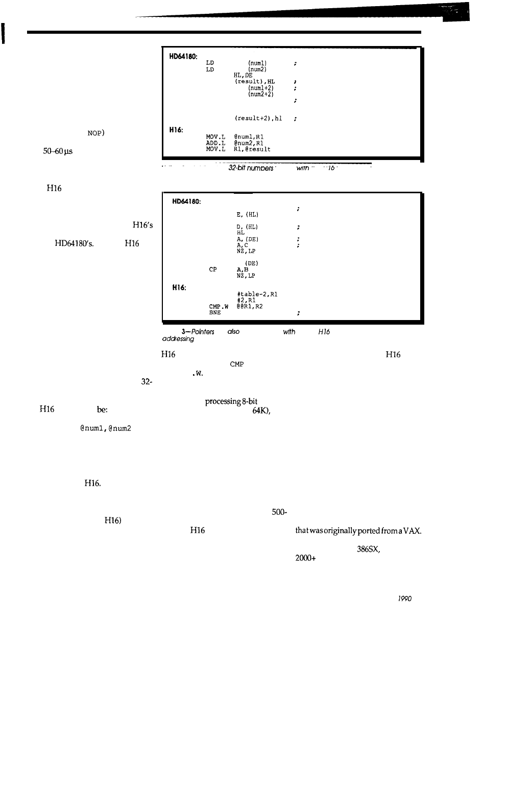
then the time is a function of the clock
rate, DMA activity, and wait states.
Further complicating matters is
the wide number of
addressing modes.
Any instruction can take literally
hundreds of forms, depending on the
source and destination arguments.
The Hitachi
data
book includes 13
pages describing timing. Some in-
structions (like a
can take only
100 ns at 10 MHz, while others can
take
(a complicated divide,
for example). It’s all but impossible to
construct a simple timing chart. Even
worse, comparing the execution speed
of the
to another processor is very
difficult without running extensive
benchmarks on both.
Fact: the
HD64180 executes most instructions
faster than the H16. Fact: the
instructions do considerably more
than the
Fact: the
can
handle 32 bits in one instruction, which
might take quite a few instructions to
simulate on an HD64180.
CODE COMPARISONS
It is often instructive to compare
code written for two different proces-
sors to see how each CPU’s architec-
ture can be best taken advantage of.
Since the BCCH16 is the successor to
the BCC180 computer, it makes sense
to compare the H16 to the familiar
HD64180.
Suppose you’d like to add two
bit numbers, as is done in Listing 2. If
we were to store the result in
num2,
the
code would
ADD.L
This is almost an unfair compari-
son! It really shows the power of
having 32-bit registers. Obviously,
multibyte math operations are much
simpler with the
Perhaps you have a table of point-
ers to data, and wish to compare a
value in a register (say BC on the
HD64180 or R2 on the
to that to
which the pointers point. The code
might look like Listing 3 if a 16-bit
compare were done (ignoring the case
where the search fails). The double
indirect mode really pays off here. If
a 32-bit compare were done, then the
ADD
LD
LD
LD
JR
INC
SKP:
ADD
LD
HL,
get low 16 bits of numbers
DE,
save low part of answer
HL,
get high 16
bits
DE,
NC, SKP
skip if no carry from low add
HL
HL,DE
; propagate carry
save high part of result
listing Z-Adding two
IS
easy
Tne H because ot its internal 32-bit
registers.
LD
HL, table
LP:
LD
BC has comparison value
HL
DE
points to comparison data
get low part of data
low parts match?
INC
LD
INC
LD
CP
JR
INC
LD
JR
DE
A,
LP:
MOV
ADD
; point to table of pointers
; point to next entry
; value the same?
LP
loop till found
;
high parts match?
listing
are
easy to work
on the
thanks to its double indirect
mode.
code would be no longer; the
CMP
instruction would be
.
L
rather
than
CMP
On the HD64180, quite a
few extra instructions would be
needed.
If you’re
data in a
limited address space (like
then
the HD64180 processor may be a bit
less convenient to use than the H16,
but is still a pretty good choice. The
H16 really shines at handling large
data items in big address ranges.
SUPPORT PRODUCTS
No CPU is an island, entire to
itself. Without decent support hard-
ware and software, even a
GFLOPS processor is worthless.
The
is a relatively recent in-
troduction, so its support base is cur-
rently somewhat limited.
The
BCCH16 single-board computer is the
most obvious support product for the
device. The BCCH16, as Tom Cantrell
described, is a complete
com-
puter on a single card. Just add a ter-
minal and power supply for opera-
tion. It comes complete with a BASIC
in ROM, so code can be generated
seconds after applying power. The
BCCHl6 is ideal for inclusion in con-
trollers and other products, since its
price is quite reasonable. It is also a
great platform for evaluating the chip
for designers considering including
the CPU in their proprietary embed-
ded systems.
Hitachi does sell a cross-assem-
bler that runs on an IBM PC. It gener-
ates Motorola S records, which can be
burned into ROM or downloaded into
an emulator. The package includes a
quite sophisticated macro assembler
No, it’s not the fastest compiler in the
world, but on my
assembling
line modules takes less than a
minute. The assembler has an exten-
sive selection of pseudo ops. The
February/March
47
.
SECTION
pseudo op lets you parti- fromSemWare,whichisimmunefrom
tion your program into apparently
hundreds of individual sections,
these problems. (At $55, Qedit is a
fantastic editor; it is WordStar
classed into up to five types (code,
data, common, stack, and dummy).
patible,veryreliable,and
for use on laptops).
The bundled linker seems to
handle even very large programs
without much trouble. Like the as-
sembler the linker is no speed demon
but is very robust.
For some reason, the odd nature
of
assembly language (with typi-
cally thousands of periods in a mod-
ule) crashes both WordStar and Mi-
crosoft Works, my two primary edi-
tors. Recently, I started using Qedit
WhiledevelopingthecodeforH16
BASIC for theH16,
Circuit Emulator from HP. To my
knowledge, there are no really good
debuggers yet available for the
(hint,
portunity for someone), so the emula-
tor was essential. Unfortunately, the
HP emulator cannot use the detailed
debugging information produced by
the Hitachi Linker. As as result, even
F
PROMOTE YOUR PC
TO
STATUS
FULLY INTEGRATED SOLUTION FOR DESIGN OF PC BOARDS
A FRACTION OF
COST OF A WORKSTATION.
CHEMA II+ schematic capture
$495
CHEMA-PCB layout with ROUTE PLOT
CHEMA-SUSIE logic simulator
$1495
$995
‘REE l-800
customer support
‘111130 day money back guarantee
FREE DEMO DISK
symbolic
debugging was unavailable.
Bill Auerbach, a local C whiz, wrote a
PC-based emulator driver for me that
annotates the disassembled code with
symbols extracted from the Hitachi
link file.
Software Environments sells an
assembler, linker, and C compiler for
the H16, but I have no experience with
these products, They can be reached
at (214) 991-0084.
Finally, Hitachi produced a soft-
ware guide for the H16 that includes
several hundred
sample code.
A number of routines are included,
such as sorts, ASCII conversions, and
math routines. This is manual num-
ber ADE-502-008, and is essential as
an introduction to writing code for the
H16. The H16 data book (book num-
ber ADE-602-003) is the bible, but lacks
examples. The software guide fills
this gap.
INTRODUCING H16 BASIC
The
without an embed-
ded language, would appeal only to
die-hard H16 fans. It seemed natural
to port the BASIC-180 language used
on the
to the
H16 BASIC resides in two ROMs
on the board. As an embedded lan-
guage, it is invoked by the reset signal;
the BCCH16 by default, with the H16
BASIC ROM set, powers up in the
BASIC environment.
H16 BASIC is an interactive lan-
guage, so you can enter, run, and
modify programs just as if you were
working on an interpreter like Micro-
soft’s MBASIC.
The BASIC is a true compiler.
When you type RUN, it converts the
tokenized BASIC code to native H16
machine language. You get the bene-
fits of an interpreter (interactive de-
velopment) with the speed of a true
compiler.
Many of you are no doubt famil-
iar with BASIC-180 from the
and Steve Ciarcia’s articles in the
February and March 1988 issues of
BYTE, so I won’t dwell on the lan-
guage’s features here. Of more inter-
est is how H16 BASIC was configured
to take advantage of the additional
resources of the
processor, and of
the BCCH16 computer board.
By now, it must be pretty obvious
that the
excels at 32-bit integer
operations.
BASIC-180 on the
HD64180 was designed to work with
integer values, since that length
is better suited to 8-bit computers. On
the H16, we elected to change this to
32 bits, giving considerably more range
to integers while costing nothing in
execution time-after all, the H16 can
do a 32-bit add or subtract in a single
instruction. There is a penalty to pay
in memory, since all integers and other
variables are saved in RAM.
Fortunately, the
huge lin-
ear address space makes it easy to
sacrifice some RAM to extended vari-
able storage. On theBCC180, we used
an elaborate dynamic mapping
scheme to take advantage of more
than 64K of memory; every task re-
sided in a different physical address
but identical logical addresses. Due to
the
memory management
unit, no more than 32K of RAM could
be made available to a program with-
out using complicated remapping
techniques.
The BCCH16 includes up to 1 MB
of RAM, in addition to the
GET TO WORK!
A New Project
Our line of macro Cross-assemblers are easy to use and full featured,
including conditional assembly and unlimited include files.
Get It To Market--FAST
Don’t wait until
the hardware is finished to debug your software. Our
Simulators can test your program logic before the hardware is built.
No Source!
A minor glitch has shown up in the firmware, and you can’t find the
original source program. Our line of disassemblers can help you
re-create the original assembly language source.
Set To Go
Buy our developer package and the next time your boss says “get to
work”, you’ll be ready for anything.
Quality Solutions
PseudoCorp has been providing quality solutions for microprocessor
problems since 1985.
BROAD RANGE OF SUPPORT
.
Currently we support the following microprocessor families (with more in
development):
Intel 8048
RCA
Intel 8051
Intel
Motorola 6800
Motorola 6801
Motorola
Motorola 6805
Hitachi 6301
Motorola
MOS Tech 6502
WDC
Rockwell
Intel
NSC 800
Hitachi
Motorola
Motorola 68010
All products require an IBM PC or compatible.
Cross-Assemblers
as low as
Simulators
as low as $100.00
Cross-Disassemblers
low
as $100.00
Developer Packages
low as
$200.00
(a $50.00 Savings)
So What
Waiting For?
Professional Development Products Group
716 Thimble Shoals
Suite E
Newport News, VA 23606
compiler in low memory. This is a lot
of space! By completely recoding the
compiler, all of the memory is
lessly available to the user. While the
HD64180 version of the language
accessed memory dynamically
through HL, limiting the logical space
to
on the H16 we use the 32-bit
registers as memory pointers. Artifi-
cial 64K limits simply disappear; ar-
rays can exceed
programs can
grow to huge sizes, and no complex
remapping ever takes place.
three phases:
editing, where the
user enters the program
where the pro-
gram is converted to machine
code
l
Runtime, where the compiled
program is executed
In all phases, certain variables
essential to the compiler are stored at
the beginning of the RAM area. About
of RAM is used for these house-
keeping variables.
The tokenized code is stored
immediately
after the RAM data area.
Tokenized code is a compressed,
ier-to-compile version of the ASCII
BASIC statements entered by the user.
Tokens can take virtually an unlim-
ited amount of space, depending on
the size of the program.
When compilation starts (i.e., the
“RUN” statement is entered),
BASIC converts the tokens to
machine code in a single pass. A sym-
bol table, used for the duration of the
compilation, is built from the end of
memory down. The compiled code is
stored immediately after the tokens.
It, too, can take an almost unlimited
amount of space. Of course, for a
simple program only a few hundred
bytes might be generated. Addresses
are assigned to the variables declared
by the programmer, working from the
top of memory on down, on top of the
symbol table. The symbol table exists
only during compilation, and
ablesonlyduringruntime,so
they
can
share the same space.
Finally, at
the compiled
code is executed where it was
CELLAR INK
piled, using the variables defined from
the end of memory. A number of
standard routines (such as support for
formatted printing) will be called by
the compiled code; these were copied
from the compiler’s ROM to the RAM
area just ahead of the compiled code
during compilation.
The linear address space does
make memory management refresh-
ingly simple.
MULTITASKING
One of the primary reasons for
H16 BASIC is its support of multi-
tasking.
Almost any real control
application requires the handling of
multiple asynchronous events. While
polled I/O is one (computationally
expensive) way of responding to
effective.
BASIC supports both tic in-
terrupts and device interrupts. De-
vice interrupts are those produced by
serial channels, DMA completion
events, and the like. These are the
most common sort of interrupts in the
process-control environment. In ef-
fect, the program never
really
needs
to
wait for I/O. When the event occurs,
a hardware interrupt signals the soft-
ware so it can take the appropriate
action.
Suppose a serial channel receives
a character. It asserts an interrupt
signal to the CPU, which immediately
suspends whatever activity it was
working on. An interrupt service
routine is automatically invoked by
the CPU to read that character and
store it in a buffer.
BASIC lets you couple a
BASIC routine to any of these device
interrupts. You could tell the BASIC
to start line 200 if your external optical
encoder passes the
mark. The
BASIC might then reset a counter
variable to zero and return.
Another use of interrupts is to
sequence activities between multiple
processes. Especially in the embed-
ded world, it is usually easy and desir-
able to segment a program into a
number of modules that execute con-
currently and independently. For
example, a keyboard scan routine
might run all the time, passing key-
strokes to the “main” routine (task)
through variables. Another routine
might refresh the displays. Each can
run independently.
BASIC uses the CPU’s timer
to generate 60 interrupts per second.
Whenever one of these interrupts
occurs, the compiler switches execu-
tion to another BASIC task. Although
a task priority scheme is implemented
(so you can make one task run more
often than another), generally most
run at equal priority. Each task thus
gets an equal share of computer time,
and an equal chance to run.
Obviously, if
BASIC takes a
long time to switch between tasks,
then an awful lot of the computer’s
resources will be wasted just with the
multitasking housekeeping.
Fast
“context switching” is thus crucial
operation.
BASIC-180 needs about 800 to
switch tasks. A big part of the prob-
lem is to completely save the state of
the CPU, all of the registers, flags, and
other CPU parameters must be pre-
served, and then those for the new
task just being invoked restored. On
the
this can be done in one in-
struction!
BASIC uses the
inter-
nal RAM as 16 banks of registers. Each
task is then assigned one of these
register sets. To save and restoreall 16
registers, the compiler simply issues a
“change register bank” instruction,
completing this tedious operation in
about a microsecond.
Of course, switching tasks is more
complicated than that.
BASIC
must decide which task is the next
eligible one to run; this is a function of
which one is the highest priority, and
which has not run for the longest time.
As a
result, task switching takes
a significant improvement over the
The
version of the BASIC
supports 32 tasks, while the BCCH16
handles only 16. This, the only trade-
off made
in the conversion, was
deemed wise because of the resulting
efficiency of context switching.
THE CONVERSION PROCESS
What does it take to convert 20,000
lines of HD64180 assembly language
to a totally new processor? Initially,
we hoped to write a translation utility
to automatically convert most of the
code. This proved impractical, since
the code was completely structured
around the limited addressing modes
of the HD64180. While it is certainly
possible to directly convert HD64180
code to
code, the resulting soft-
ware would be slow, horrible to main-
tain, and a general embarrassment.
Asaresult,werecoded,byhand,every
bit of the language.
Fewer lines of code resul ted, since
the
instructions are so much
more powerful. The number of bytes
of code increased; the
The code runs considerably faster and
the resulting shorter routines are eas-
ier to read and work on.
SUMMARY
The H16 processor is a significant
step ahead in embedded processors.
Compared to the HD64180, it offers
more performance, a better instruc-
tion set, and nice wide registers. The
linear address space makes working
on large programs much easier, and
the code runs faster as well.
The penalty? A
CPU is
always more expensive than one of 8
bits, and so will never supplant the
smaller bus widths for many applica-
tions. Even if the CPU were free, two
ROMs and two
are used even
in the simplest application. If you
need performance, the
is a good
choice.
The
board is available from
cromint
Inc., 4 Park St., Vernon, CT 06066,
671-6170, Fax:
872-2204. Call for
price and delivery.
Jack Ganssle is president of
a vendor of
microprocessor development tools. When not
down
East Coast on his
sloop.
IRS
213 Very Useful
2 14 Moderately Useful
215 Not Useful
February/March 1990
5
1
An Exercise for
FIRMWARE
FURNACE
the Student
Building
from the Ground
H
ave you ever noticed that
you learn the Really Interesting Stuff
by experience? You may spend weeks
to discover something you can sum-
marize in one sentence. But, had you
seen that sentence when you started
the project, you wouldn’t have known
what it meant; true knowledge does
not come without effort.
Several BBS discussions lately
touched on the practical aspects of
compiling
programs,
rather thanabout
the program code itself. I will start by
reviewing the essentials of
ule programs, then describe how the
MAKE utility can simplify program
creation. Finally, I will look at compi-
lation speed and how you can im-
prove it..
both
and
THE BASICS
Your first PC program undoubt-
edly fit into one disk file. Compiling
and linking were a snap and you
couldn’t imagine any other way of
doing it. But then you took on a
thousand-line project, only to discover
that one file makes for painfully slow
changes. There must be a better way!
Obviously, you must break your
source code into separate files so that
a change affects only a single file. You
recompile that file, run the linker, and
get back on the air. The linker is
generally faster than the compiler
(unless you have lots of files!), so the
edit-compile-link-test cycle becomes
fairly rapid.
Each of the source files should
contain functions that are related to
each other, which reduces the number
of references between files. I have
several standard files that always
contain the same type of routines:
STARTUP, SCREEN, PRINTER, SE-
RIAL, and so forth. In some cases, you
can reuse code from one project on the
next, although microcontroller firm-
ware is less reusable.
But working with many source
files means you must coordinate the
code. Most programs have a collec-
tion of constants to determine sizes,
addresses, and so forth; obviously,
every source file must use the same
constants! Similarly, code in one file
will refer to routines or variables in
another, so you must make some
symbols PUBLIC in one file and
TERN
elsewhere.
For assembler projects, I collect all
of the constants into a single file called
DEFINES
.
IN
C. Everysourcefilestarts
with an
INCLUDE
statement to copy
text
Thisensures that
there is one definition of each constant
and simplifies the inevitable changes.
Listing 1 shows how this works.
DEFINES
also holds structure
definitions, since often the structure is
declared in one file and used in sev-
eral others. For example,
STORAGE
.
and defines it PUBLIC, while
SETUP .ASM defines Packet as an
symbol and uses its address.
The linker connects the reference in
SETUP
to
Another
INCLUDE
file named
MACROS.
holds assembler mac-
ros.
I’ve collected a bunch of
AVMAC51 macros to simulate
DPTR
,
LJZ, and so on. Another
INCLUDE
drags these definitions into every
source file. MACROS also holds spe-
cial-purpose macros for each project.
Ed
y
Cprojects,ontheotherhand,have
a separate header file for each source
file. The headers contain constants
relating to the code in the correspond-
ing source file, as well as function
prototypes any PUBLIC routines.
Any file that needs the routines or
constants simply #includes the
appropriate header file.
The C language specifies that
variables declared outside of a func-
tion and all functions are public (the C
no need for a special keyword. If you
want a variable accessible only within
a file, add the “static” keyword to
the declaration (obvious, right?). To
reference the variable in another file,
you must use the “ext e rn" keyword
on the declaration.
It is worth mentioning that C has
a bewildering variety of options for
making variables public, external,
internal, global, local, static, or auto-
matic. Spend some time reading your
manual, because an innocent-looking
declaration can produce obscure and
baffling errors.
When a header file is included in
several source files, each variable is
declared extern in every file. One
(and only one!) file must have an
additionaldeclarationwithout
tern to tell the linker where to re-
serve storage. Listing 2 shows how
this works; you must ensure that the
header file and C source file agree on
each variable.
You can use the C preprocessor to
change the header file on the fly to
define or declare the variable depend-
ing on which source file is #include-
ing the header. Listing 3 shows how
this works; the advantage is that the
52
INK
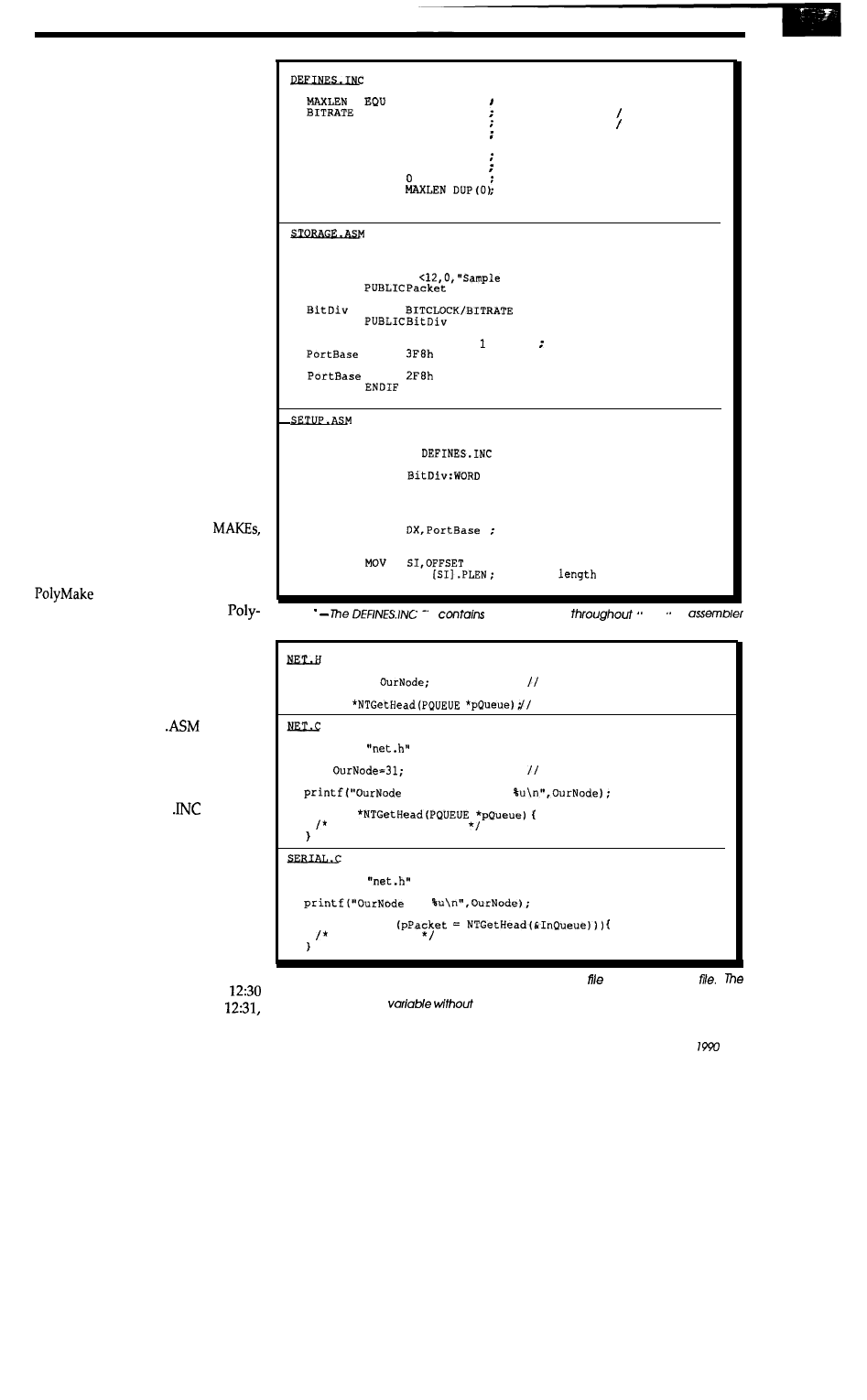
initialization information is in the
header rather than the source code
file. There is, of course, a correspond-
ing disadvantage which I’ll describe
later.
MAKE-ING A DIFFERENCE
Once you have distributed your
code among several source files, you
are faced with the fact that the simple
batch file that compiled a single file is
no longer adequate. A batch file will
recompile all of the source modules
every time you run it, so there is no
advantage to source in multiple files!
A MAKE utility provides the in-
telligence to recompile only changed
source files. Using MAKE, you never
have to recompile “everything, just to
make sure” that you didn’t forget a
file. Even better, when you change a
header file, MAKE will recompile all
of the files that include the new file. I
defy you to get that sort of relation
right by hand more than half the time.
Vanilla MAKE programs come
bundled with nearly every compiler,
third-party vendors sell
fancy
and you can find public-domain or
shareware MAKE
S
on your favorite
BBS. I have been using Polytron’s
for several years, so that’s
what I’ll use in the examples.
Make has several features that don’t
show up in other MAKE
S
, but the
basics
are
the same regardless of which
one you use.
All MAKE utilities depend on file
extensions to identify the file content.
You tell MAKE that
files pro-
duce .OBJ files and .OBJ files turn into
.HEX files, along with the exact as-
sembler and linker command lines
needed for the conversions. If some
.ASM files depend on
files, you
must also give MAKE a list of these
dependencies.
Once MAKE knows all this, it can
determine which source files are re-
quired to rebuild each .HEX file.
Unlike a batch file, however, MAKE
examines the file timestamps for each
pair of “input” and “output” files and
recompilesonly those source files with
a later timestamp. For example, if
SERIAL
.
ASM
was changed at
and
SERIAL
.
OBJ
was created
100
EQU
192
maximum packet data length
BITCLOCKEQU
serial data rate 100
1152
COMPORT EQU 1
serial bit clock 100
serial port:
1 or 2
PACKDEF STRUC
PLEN
DB
0
data packet structure definition
PTYPE DB
packet data length
PDATA
DB
packet type
PACKDEF ENDS
packet data bytes
END
INCLUDE DEFINES.INC
Packet
PACKDEF
Packet"> ; data packet storage
DW
; serial port divisor
IF
COMPORT EQ
DW
serial port address
ELSE
DW
END
MODEL LARGE
INCLUDE
DATA
EXTRN
EXTRN Packet:BYTE
EXTRN PortBase:WORD
CODE
MOV
pick up port address
MOV
AX,BitDiv ; and clock divisor
Packet
MOV
CL,
; point to packet
END
pick up
Listing
I
rile
constants used
me orner
tiles. This ensures that all files are using the same constants.
extern int
our network node address
PACKET
get head packet from queue
#include
int
set default value
initialized to
PACKET
function body here!
#include
is
if (NULL ==
and so forth
listing Z-C language
programs generally have a
header for each source
header contains variable definitions and function prototypes. At least one source tile
must declare each
the ‘extern’ keyword.
February/March
53
EXT
#ifdef NET
if NET is defined
#define EXT
then
are not external
#define INITIALIZE
#else
and they are initialized
otherwise
#define EXT extern
INITIALIZE
they are external
and not initialized
NET
EXT int
our network node address
#ifdef INITIALIZE
initialize if called for
= 31
PACKET
get head packet from queue
#define NET
#include
initialize variables
initialized to
PACKET
function body here!
SERIAL-C
#include
variables are extern here
is
if
(NULL ==
=
and so forth
preprocessor
you
TO
and definition
in one statement. Only
one
source
has a
#define NET statement, so the variable is
initialized in that
and external to others.
*TEXT EDITOR, CROSS ASSEMBLER, AND
COMMUNICATIONS FACILITY IN A COMPLETE
INTEGRATED DEVELOPMENT ENVIRONMENT
i
l
MACROS
l
CONDITIONAL ASSY
l
LOCAL/AUTO LABELS
l
SYMBOL TABLE CROSS REF
l
S OR HEX FILE OUTPUT DOWNLOADS
TO MOST EPROM PROGRAMMERS
i
AVAILABLE FOR MOST 8-BIT MICROPROCES-
SORS. CALL OR WRITE FOR TECHNICAL
BULLETIN. 30 DAY MONEY BACK GUARANTEE.
l
PER SHIPMENT:
$4 CONTIGUOUS USA
$8.50 CANADA AK, HI
Micro Dialects, Inc.
DEPT. C, PO BOX 30014
CINCINNATI, OH 45230
$15 INTERNATIONAL
(513) 271-9100
MAKE concludes that
SERIAL
.
O B J
is up to date.
MAKE uses both the time and
set your PC’s clock-calendar correctly.
While all PCs since the AT have a
battery-powered clock, you should
make sure that it is working correctly.
If you reset the clock, MAKE may
become confused about which files
are current. Take care if you have a
hour workday around the Daylight
Saving Time switchover!
Depending on how many differ-
ent processors you use, the file exten-
sions may pose a problem. An .ASM
file may contain Microsoft MASM
statements for 8086 processors, Avo-
cet AVMAC51 statements for 8051
processors, or nearly any assembler
for any processor. I use .ASM for the
former and .A51 for the latter, but
refer to .ASM
this
column
where
the distinction isn’t important.
Listing 4 shows a simplified ver-
sion of the
used with the
RTCMON debugger. There are four
main sections: source dependencies,
macro definitions, an implicit rule to
I
INK
Reader Service
3
i
PROGRAMMER $125.
Logical Systems brings you support for the Intel
The
programs this popular microcontroller on
general purpose programmers that support the 2732A. With
the
bits and the 87
ou can program the 8751 and
security
51 encryption array. Logical Systems help
you get the most out of your programming equipment
our growing line of adapters. OEM inquiries welcome.
PROGRAMS
PRICE
8744
$95.00
6744
125.00
Hitachi
65.00
JPA451 N
Signetics
(64 pin DIP)
125.00
Hitachi
(64
Low insertion force
in shrink dip)
Textool
socket
95.00
149.00
Hitachi
(64 pin shrink dip)
Low insertion force socket
ZIF
95.00
149.00
Hitachi
65.00
CALL (315) 478-0722 or FAX (315)
LOGICAL SYSTEMS CORPORATION
P.O. Box 6184, Syracuse NY 13217-6184 USA,
6715617 LOGS
1
file dependencies
cmddec.obj:
setup.obj:
storage.obj:
macros.inc
defines.inc
defines.inc
defines.inc
put temporary and
files on RAM disk
= H:
.PATH.obj = H:
generic Avocet 8031 assembly
#
this depends on having
.A51 extensions on the assembler files
PG
DEL
.MXP
how to build
rtcmon.hex
rtcmon.obj cmddec.obj
\
storage
-SP
-SN
Listing 4-A MAKE
can simplify rebuilding yourprogram because it
knows
which
depend on others.
C a c h e
RAM Disk
3
no
no
682
3
no
345
3
267
no
no
450
loo
no
300
100
264
Table --Time required to compile, assemble, and link the
program under
PC-DOS 3.3.
cache was set for
K bytes and the RAM
for 2.5 MB.
assemble source files, and a specific
ruletolink
The
source dependenciesbetween
the
#
UPDATE
and
lines
tell PolyMake that most of the .OBJ
files depend on
DEFINES
.
INC
and
MACROS.INC.
Although you can
generate this information by hand,
the MAKEDEPS program analyzes all
of the source files to find
INCLUDE
statements and inserts the depend-
ency lines between the two markers.
You must run
when
you change
INCLUDE
statements.
The two macro definitions put all
of the work and object files on a RAM
disk to
up the assembler. Al-
though this could be done directly in
the operation lines, I have learned
through experience that you never
bury disk identifiers deep in files
where they’ll come back to haunt you.
In the actual MAKEFILE, these values
are set from environment variables
defined when DOS runs
AUTOEXEC
.
read as though it said “if you need to
make an .OBJ file and have an .A51 file
around, run AVMAC51 with the fol-
lowing options and file names.” The
sourcedependenciesmentioned above
tell PolyMake what other files are
required for a particular .OBJ file.
The explicit rule
.
tells how to create the
RTCMON
.
HEX
file from a collection of .OBJ files. The
AVLINK51 program runs from a file
containing all the stuff between the
last two
signs, plus a command
line with all the switches
the
last line of Listing 4.
MAKE programs trace their an-
cestry back to the original UNIX
MAKE
S
, so obscure options and cryp-
tic switches come with the territory. It
took me months to become proficient
with PolyMake, but it now remem-
bers everything I know about rebuild-
ing all my programs...if I lose the
I’m sunk!
Because MAKE executes the
compiler as a child process, you may
find that there isn’t enough RAM for
both MAKE and the compiler.
Make comes in both large and small
varieties, but this is obviously a des-
perate move to squeak under the
byte barrier. There is a solution, but
you may not like it right away:
PUMPING PERFORMANCE
Regardless of which compiler you
use, which machine you’re using it on,
or how clever your MAKEFILE, you
won’t get results fast enough to suit
you. There are a few simple steps you
can take to improve your machine’s
performance at a reasonable cost.
I used the source code for the
and MC-Net MONITOR pro-
gram. There are 41 files containing
373K of source code, so I have a strong
interest in reducing the “compile-link”
part of the debugging cycle.
The test hardware is a 20-MHz
IBM Model
11 with 8 MB of RAM,
running either DOS 3.3 or OS/2 1.1.
The disk is a
IBM ESDI drive
rated at IO-Mbps peak transfer speed
and 28-ms average seek time.
The software I use is Microsoft C
5.10, MASM 5.10, LINK 5.03, and
PolyMake 3.1. I haven’t tried to
CELLAR INK
late the differencebetween DOS mode,
protected mode, and bound versions
of the same program, nor is this a
comparative review of forty-three
different compilers.
The results are summarized in
Table 1. Basically, you can reduce the
compile time about 60 percent by trad-
ing RAM space for disk accesses!
Compiling MONITOR with DOS
set up “straight from
without
a disk cache, RAM disk, and
takes an astounding 682 sec-
onds, over 11 minutes. The disk
sounded like it was trying to scrub the
oxide off the platters. I haven’t heard
the washer.
The disk is obviously the limiting
factor, so the best way to boost per-
formance is to reduce disk I/O. There
are at least three ways to do that: in-
crease the number of DOS buffers,
add a disk cache, and put files on a
RAM disk. All of these require addi-
tional RAM, so if you have only 640
KB or 1 MB on your machine, you
must splurge on more RAM. Fortu-
nately for all of us, DRAM prices are
dropping like the proverbial rock; you
can’t use high prices as an excuse any
longer.
DOS includes a simple disk cache
controlledby
in
Changing to 100
buffers dropped the compile time to
450 seconds, a third faster and fully
four minutes less waiting. Not bad for
a paltry50 KB of buffers and no charge
for new software!
IBMCACHE and the DOS buffers are
doing much the same thing, they have
a similar effect on performance:
IBMCACHE is better, but I gave it 200
KB more buffer space to work with.
Table
required
as-
semble, and link
program
under
OS/2 1.1. times use a 254 KB
1.7 MB RAM disk, and
Each source file gives rise to sev-
eral other files, most of which are never
read again. The disk caches don’t
know this, of course, so they discard
older data that will
in a few
seconds. A better solution is to put the
intermediate files on a RAM disk.
Although details on IBMCACHE are
skimpy, it seems to know enough not
to cache data destined for the IBM
RAM disk.
All
setup disks have a hid-
den file: the IBMCACHE disk cache
program. Once you figure out how to
install it, it works surprisingly well. In
fact, for my applications IBMCACHE
is actually better than the highly rated
disk cache supplied with Central Point
Software’s PC Tools.
Because
I set up the IBM VDISK program
for a 2.5-MB RAM disk in extended
memory. Environment variables put
all of the compiler temporary files, as
well as the .OBJ and .LST outputs,
onto the RAM disk. This, in conjunc-
tion with the cache, puts the overall
time under 270
seconds, which is
largely independent of the number of
DOS buffers.
In all honesty, all of the tests have
the compiler temporary files on the
RAM disk; I forgot to flip the
Now there
a bus that makes easy
entire family of 68000 components.
in a straightforward manner. The simplicity inherent
K-System concept allows the sys-
tem designer the ability to concentrate on meeting
demands of applications. This
same simplicity combined with low cost makes the K-System ideal for applications
ranging from personal use through educational and laboratory applications up to industrial
control and systems development. All
is accomplished at saciiice in performance
or
The
size (4 5 inch) the K-Bus boards permits the optimal division
of system functions thus simplifying system configuration. The motherboard incorporates
integral card guides and compatible
power connectors which minimizes packaging require-
ments. Both SKDOS and
are fully supported allowing
system
utilization in both
and multi-user application;.
Boards currently in production:
FORM
K-SCSI
K-DMA
K-xxx-BB
12 Slots,
PC type power
$129.95
CPU, 2 ROM
(12 or
$129.95
RAM or 27256 type EPROMs (OK installed) 59.96
2 serial pons
full modem
(68681)
99.96
disk controller (up four drives)
99.95
Full SCSI implementation
chip
99.96
2 channel
using
chip
$129.95
General
board
39.95
Bare board
documentation for above
39.95
SKDOS
Single user, editor, assembler,
BASIC
$150.00
Multi-user,
assembler, SCRED,
BASIC,
C, PASCAL, FORTRAN are available
$300.00
Inquire about our
line of
Single Board Computers.
Q u a n t i t y a n d p a c k a g e d i s c o u n t s a v a i l a b l e
Terms: Check, Money Order, Visa,
include UPS ground shipment in
continental U.S.
Hazelwood Computer Systems
Highway 94 at
MO 65069
l
(314) 236-4372
58
Featuring
l
Standard RS-232 Serial Asynchronous
l
48 Character LCD Display (2 Lines of 24 each)
l
24 Key Membrane Keyboard with embossed graphics.
l
Ten key numeric array plus programmable function keys.
l
Four-wire multidrop protocol mode.
l
Keyboard selectable SET-UP features-baud rates, parity, etc.
l
Size (5.625” W x 6.9” 1.75” Weight 1.25
l
5 7 Dot Matrix font with underline cursor
l
Displays 96 Character ASCII Set (upper and lower case)
Options-backlighting
for
RS-422 20 Ma current loop
302 N. Winchester
l
KS 66062
l
ment variablesand didn’t want to blow
the rest of the day taking the measure-
ments again. Had the temporary files
gone to the hard disk, the no-cache
times would be even worse.
With both the cache and RAM
disk in effect, the hard disk light blinks
when
starts the compiler
on a new file. Because all of the com-
piler passes don’t fit into the cache, it
is flushed for every source file. Some
informal tests I did indicate that a
KB cache doesn’t improve things much
because the disk is such a small part of
the overall compile time. The process
is now CPU bound!
Whatdoesthismeanforyou? First
of all, if you do not have enough RAM
to take advantage of disk caching, buy
some. Then, jacking up the
B U F F
-
ERS
=
or installing a disk cache will
give you the biggest win. Putting
temporary files on a RAM disk is a
lesser win, but still worthwhile.
If you are using a 286 AT clone,
EMS expanded RAM is the only way
to go because it is somewhat faster
than extended RAM. Clones with a
386 can use the processor’s memory
mapping hardware to convert ex-
tended into expanded RAM, so all
you need do is buy the RAM and
something like Quarterdeck’s QEMM
to handle the mapping.
MULTI-WHAT?
Of course, you can break the
KB barrier and take advantage of that
new RAM directly by switching to
Although that sounds suspi-
ciously like an ad, it turns out to be
true. I have been using OS/2 as my
“development platform” since last
summer, and I’m well pleased with
the results. Just for completeness, I
ran the performance tests under
OS/2 as well.
Table 2 summarizes the OS/2
results on the same hardware. The
fact that OS/2 takes longer to compile
MONITOR is not surprising, because
OS/2 has mode switching overhead
during interrupts. The fact that the
DOS Box takes only 17% more time
than DOS is surprising, particularly in
light of all the early doomsayers.
But the DOS Box isn’t multi-
tasking, so a better comparison is with
a protected mode compile. OS/2 takes
about half again as long as DOS to do
the compile, nearly seven minutes
versus
Ouch! However, when
the compile is put into the background
the time increases only a few more
seconds, which is
comforting.
Does this mean OS/2 is a piece of
junk? The answer to that may be the
biggest surprise of all: no!
Remember that MAKE compiles
only changed files.
Rebuilding
MONITOR after editing one file takes
less than a minute in either environ-
ment, so the difference is irrelevant; it
takes that long to sit back, stretch, and
check the birds at the feeder.
Balanced against the increased
compile times are all the advantages
of
real multitasking, relief from
the 640K limit, largely crashproof
debugging, and an improved operat-
ing system interface. Even though
most of the programs I develop are
meant for real-mode execution, OS/2
is a better development environment.
Indeed, MONITOR would be an
ideal protected-mode program. I had
to write a special-purpose multi-
tasking kernel for it;
OS/2 pro-
vides far better multitasking built into
the operating system. One of these
days I’ll have to convert it and see how
much code “goes away.“
If you, like most people, have
dismissed OS/2 as something for the
future, it is time for another look. If
you develop code for a living, the
future is now.
AND THEY’RE OFF!
This is INK’s second anniversary,
so, once again, it’s time for you to give
me some guidance on what you’d like
to see here in the upcoming year. Send
me a BBS message to tell me where to
Ed
is member of the Circuit Cellar
makinggizmosdo
strangeand wondrous things.
by turns,
a beekeeper, bicyclist, Registered Professional
Engineer, and amateur raconteur.
IRS
2 16
Very Useful
2 17 Moderately Useful
2 18 Not Useful
COMMUNICATIONS
508-485-1144
COLOR SUPER
VGA
MONITOR
LIKE NEW 6 MONTH WARRANTY . . . . . . . . . . . . . . . . .
USED 3 MONTH WARRANTY . . . . . . . . . . . . . . . . . . . . . . . . . . . $600.00
USED WITHOUT CASE . . . . . . . . . . . . . . . . . . . . . . $300TO $500.00
19” COLOR SONY 1280 X 1024 . . .
THESE SONY TRINITRONS HAVE A FULL 6
WARRANTY PARTS AND
Q
IKEGAMI
64KHZ 1280X1024 NEW . . . . . . . .
16” PANKSONIC
USED . . . . . . . . . . . . . . . . . . . . . .
14”
VGA CHASIS . . . . . . . . . . . . . . . . . . $249.00
1 YEAR WARRANTY
19” PHILLIPS 1024X800 48 KHZ GRAY SCALE . . . . . . . . . . . . . . . . . . $350.00
1 YEAR WARRANTY MAY BE ORDERED FOR VGA AT NO EXTRA CHARGE.
WHEN USED IN
VGA
MODE THE MONITOR WILL RUN
X 600 X 256
SCALE
OR
SCALE ONLY
CALL US ABOUT OUR
LARGE
VARIETY OF GRAPHIC CARDS
194 Main ST.
01752
February/March
59
Building an LED Moving Message Display
H
ow many times have you heard,
The opportunity presented itself the next afternoon,
just be a minute Honey, we only
just before leaving work. “Mrs. Jeff on line four,” was the
P
a e. I punched the flashing button on my desk phone.
‘We need milkonyour way home. Bothkinds: regular and
need a couple of things,” as your wife
“Already?” I gasped. I knew this was it. “OK, see
ya soon,” I answered, ending the conversation. The phone
disappears into the supermarket?
cord was still swinging as I exited in a dash, one arm
already threaded through a coat sleeve.
could count on one hand the items to
You find the strangest people in the grocery store.
From people with calculators who know what their bill
will be even before they get to the register, to moms who
purchase: milk, bread, snacks, and
nng their kids along to help and end up with more
cookies, candy, and cereal than anything else. Something
freshly sliced meats from the
seemed different today. Every aisle contained people
standing around, looking up as if there were fireworks on
still while their drivers stood reading scrolling
those
bright
yellow diagonally painted
ments hanging from the ceiling like circus trapezes. Three
and four displays in every isle, each with its own
lines which
to
constantly
.
10 for 99 cents-get SLICK disposable razors.”
“Can’t you read, jerk? NO PARKING
“DOUBLE COUPON item-Minute Mash, now
It was mesmerizing and worse,
ing. There was no way to avoid them. Displays so big and
I kept muttering to myself,
you could read them from 50 feet away.
“She’ll be right out, wait here one
“Milk, ah yes,” I thought. Spinning around after
finally getting my bearings,
I
made my way to the dairy
cooler. There were feeding frenzies taking place at various
thestore. Obviously, theadvertisingblitzes were
effective. I grabbed the milk and left without spending
what was so time consuming. Were
more than an additional $18. Not bad for 43 minutes.
the bakery? I had to know!
6 0
CIRCUIT
INK
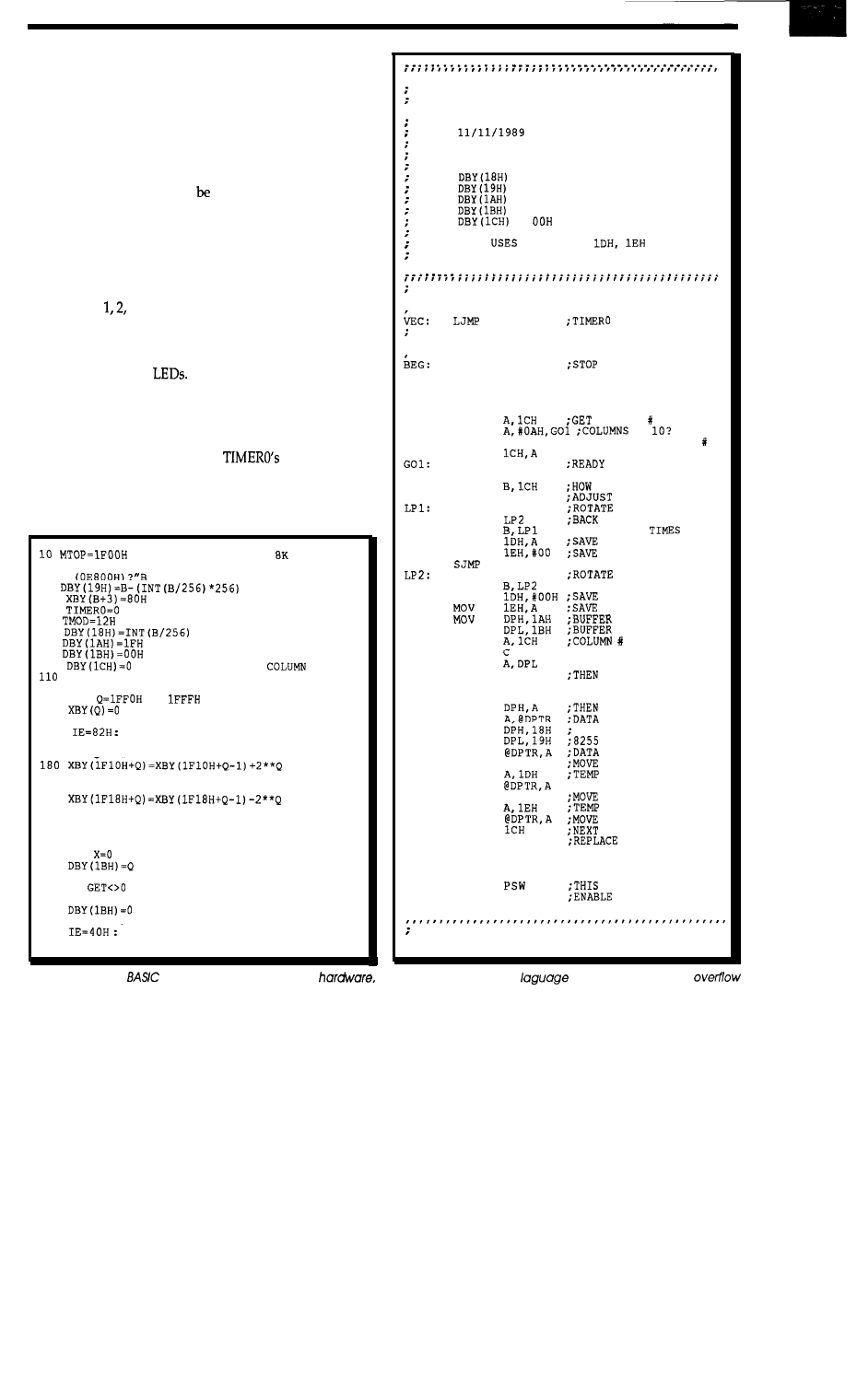
UNNATURAL RESOURCES
New technologies are constantly gobbled up by the
advertising media. One benefit of their prolific use is to
bring
down
the
price of technology to a point where we can
put it to a more productive use.
My last column described the basics of LED displays
and included a small project: an 8x10 LED array display.
Although it was designed
to
used with any 8255 PPI, the
RTC52 and RTCIO were chosen as the engine because
most of the readers are familiar with them.
[Editor’s Note:
For more information abouf the RTC52 and RTCIO boards, see
“From the Bench” in the April/May 1989 issue of C
IRCUIT
C
ELLAR
INK.1
Before moving on, let me present the software
promised for the 8x10 display presented last issue.
Listings
and 3 show sample code which updates
the display as a background task running on an RTC52.
BASIC can be used to manipulate data in the RAM used as
a display buffer. A ten-byte display window mapsdirectly
to the ten columns of
The background routine grabs
data one byte at a time and applies it to port A of the 8255.
Ports B and C enable each column in sequence, one per
interrupt. Even though only one column is active at a time,
the persistence of our retinas blurs the separately enabled
columns into a coherent image.
overflow inter-
rupts BASIC and displays the next column’s data. At the
end of each interrupt, it’s back to BASIC again until the
next overflow.
:
REM IN CASE ONLY
RAM
20 INPUT "WHAT IS THE 8255 BASE ADDRESS
30
: REM 8255 LSB
40
: REM CONFIGURE AS ALL OUTPUTS
50
60
:
REM TIMER0 = 8-BIT AUTO RELOAD
70
:
REM 8255 MSB
80
:
REM BUFFER MSB
90
:
REM BUFFER LSB
100
:
REM START WITH
ZERO
REM NOW FILL THE DISPLAY BUFFER WITH NULL
DATA
120 FOR
TO
130
140 NEXT Q
150
REM THIS ENABLES THE DISPLAY
160 REM PUT SOME DATA INTO THE BUFFER
170 FOR 0=0 TO
1
190 NEXT Q
200 FOR Q=O TO 7
210
220 NEXT Q
230 PRINT "HIT ANY KEY TO STOP"
240 REM NOW MOVE THE DISPLAY BUFFER LSB
250 FOR Q=O TO 20H
260 FOR
TO 5 :
NEXT X :
REM DELAY LOOP
270
280 NEXT Q
290 IF
THEN 310
300 GOT0 250
310
:
REM POINT TO NULL DATA
(
B L A N K
DISPLAY)
320
REM TURN OFF INTERRUPTS
330 END
listing 1
-A
sample
program
that initializes the
enables interrupts, and updates the display memory in the fore-
ground.
8 X 10 LED ARRAY DISPLAY
JEFF BACHIOCHI
REQUIREMENTS:
= 8255 BASE ADDRESS MSB
= 8255 BASE ADDRESS LSB
= DISPLAY BUFFER ADDRESS MSB
= DISPLAY BUFFER ADDRESS LSB
=
(
S T
A R
T A
T
COLUMN ZERO
)
ALSO
REG
I
S T E
R
S
AS
TEMPORARY STORAGE
ORG
400BH
BEG
INT VECTOR
ORG
4200H
CLR
EA
ALL FURTHER INTS
PUSH
ACC
;AND SAVE ALL REGS USED
PUSH B
PUSH
DPH
PUSH
DPL
MOV
COLUMN
CJNE
=
CLR
A
;IF SO RESET COLUMN
MOV
SETB C
TO ROTATE
CLR
MOV
INC
RLC
JC
DJNZ
MOV
MOV
RLC
DJNZ
MOV
IT:
MOV
MOV
CLR
ADD
MOV
CLR
ADDC
MOV
MOVX
A
B
A
IT
A
DPL,A
A
A,DPH
MANY TIMES?
IT
TO START?
;DO UP TO 8
IT FOR PORT B
ZERO FOR PORT C
;DO UP TO 2
ZERO FOR PORT B
IT FOR PORT C
MSB
LSB
AS OFFSET
;ADD IN OFFSET
REPLACE
;ADD IN ANY CARRY
REPLACE
FROM BUFFER
MOV
8255 BASE MSB
MOV
BASE MSB
MOVX
TO PORT A
INC
DPTR
TO PORT B
MOV
DATA
MOVX
;TO PORT B
INC
DPTR
TO PORT C
MOV
DATA
MOVX
TO PORT C
INC
TIME NEXT COLUMN
POP
DPL
ALL REGS USED
POP
DPH
POP
B
POP
ACC
POP
ONE NEEDS POPPING
SETB EA
INTS
RET1
;OUT-A-HERE
. . . . . . . . . ..**...................................
END
listing
2-This machine
hand/es the TIMER0
interrupt jump vector and outputs the contents of the display
memory in the background.
February/March 1990
6
1
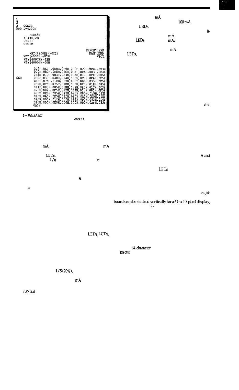
510
520
530
540
550
560
570
580
590
600
610
620
630
640
650
670
680
690
700
710
720
730
740
750
REM APPEND THIS IF USING A 32K RAM
REM TO LOAD THE INTERRUPT ROUTINE
500
: C-O
READ B
IF
THEN 570
GOT0 510
IF Co33627 THEN PRINT "CHECKSUM
IF
THEN PRINT "NO
: REM INST. TIMER0 JUMP
RETURN
DATA
DATA
DATA
DATA
DATA
DATA
DATA
DATA
DATA
DATA
DATA
DATA
DATA
listing
program can be appended to Listing1 to
poke Listing 2’s object code into RAM at
E-X-P-A-N-D-l-N-G ON THE IDEA
The maximum average current for an LED in these
arrays is about 20
with peak currents of about 100
allowed. Peak currents come into play when we multiplex
rows or columns of
When multiplexed, each row or
column is on for only
of the total time (where is the
number of rows or columns and duty cycle is l/n times
100%). So, for a row or column LED to appear to be the
same intensity as a nonmultiplexed LED which is always
on, the row or column LED must be times brighter.
Fortunately, the current necessary to do this is somewhat
less than times because the efficiency of an LED goes up
as the current increases. As the number of columns in-
creases, the duty cycle becomes smaller, until finally even
boosting the LED current to the maximum allowable will
not produce enough intensity for the display to be seen
clearly.
Let’s take the relatively simple project presented last
issue and expand it into a scrolling sign similar to the ones
you see in stores, airports, and sports bars. The intent of
the design is to give a highly visible display to applications
where dangerous conditions exist. Single
and CRTs can all be used for status conditions, but in many
applications the operators may not be within range to
easily read such information. Using a large LED display
can communicate important information to anyone imme-
diately without a fifty-yard dash. To eliminate the prob-
lem of increasingly smaller duty cycles, we treat each 5x8
module as a separate entity. Each module would have a
maximum duty cycle of
eliminating the con-
trast and maximum peak current problem. Designing for
a maximum LED peak current of 100
(which, at a 20%
62
CELLAR INK
duty cycle, is equal to 20
average
current)
sounds easy,
but finding a standard device to sink
for each of
eight column
is not. After perusing many data
books, I came across a Sprague part which contains an
bit latch capable of sinking 100
for each of the eight
bits. With all
on, that’s 800
not too shabby since
most TTL devices have a tough time with 20 mA/bit.
Now that we can sink the 800
coming through the
column
we must be able to source and control it. A
plain old PN2222 had the oomph I was looking for, capable
of handling up to one amp of collector current. Refer to
Figure 1 for the schematic of the expandable array display.
Note that circuitry for only one array module is shown.
This is duplicated eight times on the board, once for each
display module.
NEW CIRCUITRY-OLD RULES
To ease the design and implementation of this new
display, we will keep the same restraints as before: the
play’s control will come from the three ports of an 8255, but
this time with a bit more functionality assigned to each
port. Port A will pass column data to the arrays. The first
five bits of port B will be column enables and the last three
will be module enables. Port C will consist of eight board
enables. Each board will control eight 5x8 LED array
modules. Up to eight boards can be used, totaling 64 5x8
LED arrays (that’s six feet worth of characters!). When a
board is enabled by port C, the top three bits on port B are
decoded into a strobe for one of the eight modules on the
board. Thisstrobelatches thecolumndata from port
the column enable from the lower five bits on port B. Each
module has its own data latch and a column latch which
holds the module’s column
lit until the next access to
that module.
With the above system, any one of the five columns on
any one of the eight modules on anyone of the eight boards
can be latched with the data on port A. A single-board
system can display up to eight characters while an
board system can display up to 64 characters at a time. The
or horizontally for an x 320-pixel display. The informa-
tion displayed is limited only by your imagination and
programming ability.
THE NECESSARY EVIL-SOFTWARE
The code developed for this project allows any one of
32 &character canned messages to be scrolled through
the display using from one to eight display boards. Alter-
natively, a
messagecanbe entered live through
the
or RS-485 port of the RTC52 used to control the
display. Scroll speed can be adjusted from the keyboard,
or the display can be set into a nonscrolling mode to
display a short, constant message. A portion of the system
RAM is set aside for use as a display buffer. The beginning
of the display buffer is first padded with null data, which
allows the display to start blank. Next, each character of
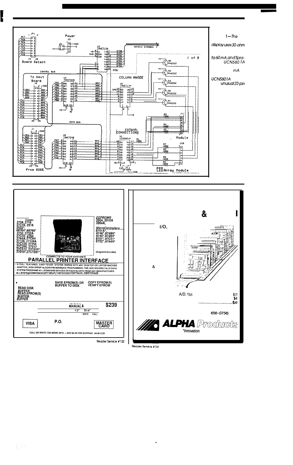
CONNECTIONS
ROW
C o n n e c t i o n s
con
R e e a t f o r e a c h
5 x 8
Figure
ex-
pandable array
series resistors to
restrict LED current
g u e
latches
capable of
sinking 100
on
each
b i t .
The
comes
in an
0.4inch-wide DIP
package.
MS-DOS EPROM
PROGRAMMING SYSTEM
NEEDS NO INTERNAL CARD
EPROMS
2708
2564’
28256’
8742
‘Socket Adapter
Required
SYSTEM SOFTWARE COMMANDS
PROGRAM EPROM(S)
FROM DISK FILE
l
:
l
FILE INTO . PROGRAM EPROM(S)
ERASED
FROM BUFFER
. BUFFER EDITOR
.
INTO . COMPARE EPROM(S) . SELECT DEVICE TYPE
WITH BUFFER
. DEVICE CHECKSUM
ED/TOW
HAS 18 BYTE LEVELCOMMANDS FOR DETAILED OPERATIONS
SYSTEM INCLUDES: PROGRAMMING UNIT POWER PACK
CONNECTING CABLE, OPERATION
SOFTWARE’
SOFTWARE AVAILABLE ON 3
OR
DISK
TO ORDER SEND CHECK, MONEY ORDER.
OR
ANDRATECH
BOX
222
MILFORD, OHIO 45150
(513) 831-9708
A-BUS”
Data Acquisition Contro
Low Cost A/D, Motion Control, Relays,
D/A, Digital
Counters...
Sample Applications:
Read sensors. voltages,
light levels, temperatures,
keypads, touch-tones:
Switch electrical devices:
Automate experiments:
Test equipment.
Bus adapters for:
PC/XT/AT compatibles:
Apple II: Tandy and
others. Or use RS-232
serial adapters
for remote
applications
New Products
FA-154: 12-bit 8-channel
MC-l 08: Metal
. . . . . . . . . . . . . . . . . . . . . . . . . . . . . . . . . . .
cover for Motherboard . . . . . . . . . . . . . . . . . . . . . . . . . . . . . . . . . . .
AC-l 09: Acrylic cover for Motherboard
Call for new catalog: (203) 6564806
Mon-Fri 9-5 Eastern time
(or Fax 203
through Application”
242-C
West Avenue, Darien, CT
06820
February/March 1990 63
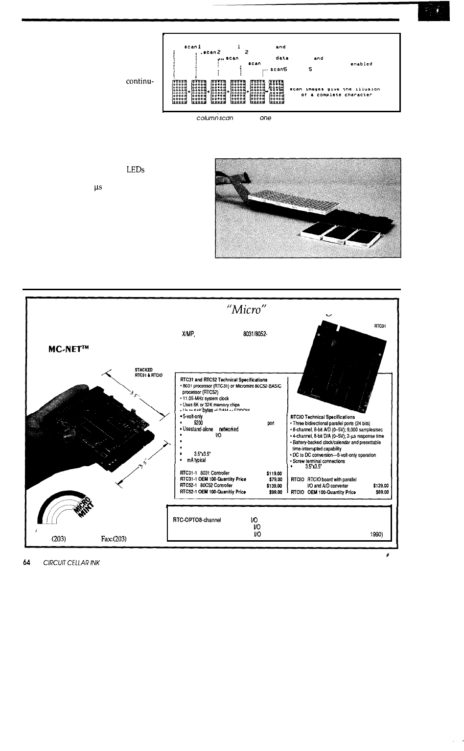
the message string is converted into dis-
play data using a look-up table.
. . . .
column
data latched
e n a b l e d
Finally, the display buffer is filled to
column data latched and enabled
3 c o l u m n 3
l a t c h e d
e n a b l e d
the end with null data. Once the hard-
. . . .
4 column 4
data latched and
ware is initialized and the interrupts
are
c o l u m n d a t a l a t c h e d a n d e n a b l e d
enabled, the background code
ally transfers the data held within the
display buffer into the latches for each of
the 64 possible LED array modules. The
.
routine is fed with buffer start and end
Figure 2-Each
displays
strip of the total character. Our eyes merge
addresses and a scroll or no scroll flag.
these into one.
At each interrupt, the service routine
must transfer data for one column of each module on each
board, and must be short enough to update up to 64
modules five times, once for each column, at a rate which
fools the eye into thinking all the
are on at once. This
routine, the results of which are shown in Figure2, takes a
maximum time of 200 every 4 ms. That’s 20 ms for five
scans, one for each of the five columns, or 50 Hz, which is
about the minimum time for our eyes to see one image.
If in scrolling mode, the interrupt routine must also
determine at which point to move the scroll window. The
scrolling window
shown
in Figure 3 is a view of the
display buffer. It is the scroll window that moves through
the display buffer and not movement of the data in the
buffer that gives the illusion of scrolling. A scroll counter
is decremented once each scan. When the scroll counter
reaches zero, thescroll window isadvanced. Thecounter’s
MICROMINT Introduces
Controlling!
After years of experience in manufacturing OEM controller boards and talking to customers, we think we have
hit upon just the right combination of format and function to satisfy even the toughest case of “relay mentality.”
Realizing that not every computer/controller application warrants a Cray
Micromint offers a tiny
based controller board for those dedicated and cost-sensitive installations.
New
software links your desktop up to 31 RTC controllers.
Up to
64K
of RAM or EPROM
operation
11 O-1
bps AS-232
and/or
RS-485
serial
or
12
bits of
parallel
Vertical-stacking expansion bus
Screw
terminal connections
Small
format
60
operating current (RTC52)
Small
format
Micromint, Inc.
4
Park Street, Vernon, Connecticut 06066
Tel:
871-6170
l
872-2204
Available Soon!
Optoisolated Expansion Board (expected availability December, 1989)
RTC-SIR Serial, Timer, and Infrared Expansion Board (expected availability January, 1990)
RTC-LCD LCD, Keyboard, and X-10 Expansion Board (expected availability February,
Reader Service 137
C
IRCUIT
C
ELLAR
INK’s
ADVERTISER’S INDEX
Reader Service
Number
101
102
103
104
105
106
107
108
109
110
.
111
112
113
114
115
116
117
118
119
120
121
162
122
123
124
125
126
127
128
129
130
131
132
133
134
135
136
137
138
139
140
141
142
143
144
146
147
148
149
150
145
151
152
153
154
155
156
157
158
159
160
161
Advertiser
Alpha Products
Andratech
Ariel Corp.
Avocet
Baradine
Berry Computers
Big Bang Software
Binary Technologies
Cabbage Cases
Catenary Systems
Ciarcia Design Works
Circuit Cellar
Circuit Cellar
Computerwise
Cottage Resources
Covox Inc.
Industrial
Emerald Microware
Engineers Collaborative
Express Circuits
F&W Communications
GTEK
Gott Electronics
Grammar Engine
Hazelwood
Information Modes
lnnotec
Corp
Kolod Research, Inc.
Laboratory Microsystems
Lear Corn Company
Logical Systems
Meredith Instruments
Micro Dialects, Inc.
Micro Digital
Micro Resources
Micromint
Micromint
Micromint
Micromint
Ming Engineering
NOHAU Corp
Omation
Paradigm Systems
Parallax, Inc.
PI Computer
Quinn Curtis
D Electronics
Real Time Devices
Ryle Design
Sierra Systems
Silicon Alley
Sunnyside Solar
Systronics
Tardis Systems
Tinney
Traxel Laboratories Inc.
Unkel Software
Louis E. Wheeler
Associates
Wytec Company
Page
Number
63
63
75
4
67
27
78
57
57
11
55
13
11
49
28
79
54
79
40
16
6
50
11
35
70
71
79
28
ASSOCIATES
NATIONAL ADVERTISING SALES
REPRESENTATIVES
NORTHEAST
Lisa
Tel:
769-8950
Fax:
769-8982
MID-ATLANTIC
Barbara Best
741-7744
SOUTHEAST
Collins
966-3939
Fax:
MIDWEST
Nanette Traetow
Tel:
789-3080
Fax:
789-3082
WEST COAST
Barbara Jones Shelley Rainey
Tel:
540-3554
Fax:
540-7103
SUBSCRIPTION
PROBLEMS?
I
have problems with your
subscription (delayed or miss-
ing issues, change of address,
or
questions on renewals), call
the Circuit Cellar INK Sub-
scriber Service Line at
628-0885 or write:
Circuit Cellar INK
Subscriber Service Dept.
P.O. Box 2099
Mahopac, NY 10541
IRS
INK
Rating Service
How useful is this article?
At the end of each article and some
features there are 3-digit numbers by
which you can rate the article or fea-
ture.
Please take the time to let
Circuit
Cellar INK, know how you
our ma-
terial rates with you. Just circle the
numbers on the
card.
February/March
65
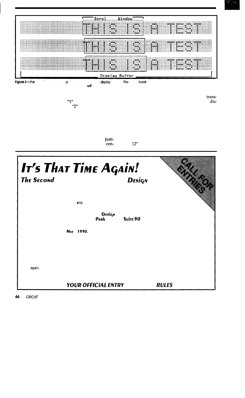
l i n s
scrolling window is limited view into the
buffer.
buffer
all the data used to display a message while
the window selects which section of the buffer be displayed,
reload value controls the scroll speed. The user can adjust
version routine (specifically the number of columns
the reload value by using the
key to speed it up (de-
ferred for each character), any width character can be
crease the reload value) and the
key to slow it down
played. Define your own size character set or use one from
(add to the reload value).
a font editor. The upper 128 characters of the ASCII table
could be defined as graphics characters similar to those in
CUSTOM CHARACTER CONVERSION
the IBM character set.
The character conversion is done for a 5x7 character
THE SMART DISPLAY
with a leading blank column. The high bit is off in each
column, which makes the 5x7 character lower-right
The physical dimensions for the display board are 2.4”
fied in a 6x8 block. With minor modifications to the
high by
long. Total LED current could be as much as
C
I R C U I T
C
E L L A R
I N K
C
O N T E S T
Yes, sports fans, it’s time to sharpen your pencils, heat your soldering iron, and sort through your chip collection,
because the Second C
IRCUIT
C
ELLAR
INK Design Contest is here! This year, the emphasis is on creativity, with solid
design, a unique approach, and an eye to elegant utility being keys to a successful entry.
Each entry must be accompanied by an Official Entry Form. To receive an Official Entry Form and complete set of
rules, send a self-addressed, stamped
envelope to:
C
IRCUIT
C
ELLAR
INK
C
O N T E S T
4
S
TREET
,
V
E R N O N
,
C T
0 6 0 6 6
All entries must be received by
4,
An individual may enter more than once, but each entry must be received separately,
and must be accompanied by an Official Entry Form. Winners will be announced in the August/September 1990 issue of C
IRCUIT
C
ELLAR
INK.
PRIZES!
Yes, of course there are prizes! First prize is worth $500, Second Prize is worth $200, and Third Prize is worth $100. In addition, the
judges may award Honorable Mention Prizes that consist of $50 and a one-year subscription (or extension) to C
IRCUIT
C
ELLAR
INK.
TWO CONTESTS IN ONE!
Once
there are two categories: Open and Cost Effective. The Cost Effective category seeks to reward those who work with
simple, low-cost controllers and processors in cost-effective designs. Identical prizes will be awarded in both categories. Placement
of an entry into a category is at the sole discretion of the judges.
SEND FOR
FORM AND
TODAY!!
CELLAR INK
6.4 amps with all
on, depending on the value se-
lected for the series resistors. In reality, average current
consumption is about two amps per board unless you
choose to display black on white (or red). A 26-conductor
ribbon cable carries the control signals to each board
attached in a daisy chain configuration. A dedicated LED
power supply is attached to each board separately, reduc-
ing the wire size necessary to supply maximum current to
all boards.
Because of the small physical size of the RTC52 micro-
controller system, the microcontroller can be easily con-
tained within the same enclosure as the display. This pro-
duces a compact unit capable of stand-alone operation as
well as a smart display using RS-232 or
as a commu-
nication interface.+
Bachiochi
“BAH-key-AH-key”) is a member of the
Circuit Cellar
His background includes
both the electronic engineering and manufacturingfields. In his spare
time,
enjoys
his family, windsurfing, and pizza.
IRS
2 19
Useful
220 Moderately Useful
221 Not Useful
The following items are available from
Circuit Cellar Kits
4 Park St., Suite 12
Vernon, CT
875-2751
1. Blank PC board, manual, and demo software on 5.25”
2. Eight Sprague
driver chips. SD-2
$20
3. Eight
red 5x8 LED array modules. SD-3
Please add $3 shipping and handling in U.S.; $8 elsewhere.
Innovations like these help to make today’s technology more cost-effective,
reliable, and easier to use. Please share your favorite ideas, chips, and circuits
with others.
We will pay $25 for any From
Bench accepted for publication. All
submissions should be typed, double-spaced, and include neatly drawn sche-
matics or Schema configuration, library, and page files.
Include astamped, self-addressed envelope large enough to hold everything
if you wish materials that have not been accepted to be returned.
Submit to:
From the Bench
Circuit
Cellar
INK
Box 772
Vernon, CT 06066
A
rugged
CASE? lined
plenty ot foam for
your equipment can
TAKE A LOAD OFF YOUR MIND
when you’ve got to travel.
TAKE A LOAD OFF YOUR BACK
with our exclusive tilt-wheels
and extension handle
a
UNLOAD ON US!
Call or write to tell us about your
shipping or carrying problems
WE HAVE SOLUTIONS!
C A B B A G E C A S E S , I N C .
1 1 6 6 - C S T E E L W O O D
R O A D
COLUMBUS,
43212-1356
( 6 1 4 ) 4 6 6 - 2 4 9 5
DEBUG
PROGRAMS
ON YOUR PC
and
SIM20 are
software simulations of
the
and MC68020
designed
to run on the IBM PC and compatibles with DOS
2.0 or higher. No additional hardware required.
They accept files generated by a
assembler. They are complete debugging tools,
providing access to registers, flags, and memory.
All
instructions, addressing modes
and condition codes are supported.
l
Load/Dump Facilities
l
Disassembler
l
Single-Step Fast Execution
l
Breakpoints
l
Interrupts
l
Terminal I/O Support
l
Symbolic Debugging
l
Execute Batch Files
(MC68020) . . . . . . . . . . . . . . . . . . . . . . . . . . . . $345
BIG BANG SOFTWARE, INC.
Hwy.
Suite 286
Panama City Beach, FL USA 32407
Phone
Fax
R e a d e r
February/March 1990 67
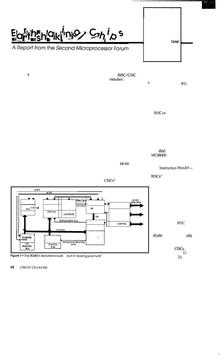
SILICON
UPDATE
Tom
A
I write this, the dust is still settling from the
“almost big one” that hit Northern California October 18.
If you’re ever in
an
earthquake,
just remember it’s like surf-
ing on solid ground. If you can’t surf, move to Kansas.
Even a 7.1 won’t stop the wizards of Silicon Valley for
long (now an 8.1, that’s another story!). They’re hard at
work on the chips that will shape the next era of the
microelectronics revolution.
I recently attended the Second Annual Microproces-
sor Forum-a two-day conference, hosted by Mike Slater,
editor of the Microprocessor Report newsletter. The Forum
brings together the
key
academic and industrial micropro-
cessor gurus to predict (and promote their version of) the
future. Judging from this
year’s
gathering,
the
chips of
the
’90s will be shaking things up too.
‘ISC WARS
There are three aspects of CPU design which deter-
mine performance: architecture, implementation, and
technology. A good analogy is a building, whose “per-
formance” is arguably the combination of design (archi-
tecture), construction (implementation), and materials
(technology). Often these factors overlap, making it hard
to separate their respective influences.
DATA BUS
I ,
I
DATA BUS
I
LINEAR ADDRESS BUS
,
I I
BARREL
SHIFTER
BASE, SEGMENTATION
, CACHE
BUS INTERFACE
I N D E X
UNIT
PAGING
“ N I T
REGISTER
BUS
DESCRIPTOR
UNIT
R E G I S T E R S
ADDRESS DRIVERS
ADDRESS
BYTE
TRANSLATION
CACHE
ALU
DO-D31
ATTRIBUTE
DATA BUS
PLA
BUFFER
TRANSCEIVERS
BUS
MICRO-INSTRUCTION
PREFETCHER
CONTROL
BUS
32 BYTE CODE
OUEUE
UNIT
DECODE
CONTROL UNIT
In this era of “Complex
and “Streamlined
some argue that the terms RISC and CISC have
become technically mean-
ingless. CISC proponents
point out that many of the
claimed innovations at-
tributed to RISC-cache,
multiregister sets, de-
layed branches, etc.-are
not really new. In the ab-
sence of technical differ-
ence between
and
CISC, the marketing defi-
nition applies: the Intel
and Motorola
family are CISC, anything
else is a RISC.
The
war continues to dominate the indus-
try
For those of you who don’t already know my
opinion (“RISC vs. Reality,
C
IRCUIT
C
ELLAR
INK
I’ll
state it again.. .
*The ‘ISC warriors often confuse architecture, im-
plementation, and technology. Caching and pipelining
are implementation techniques which have little to do
with (Instruction Set Architecture). Certainly, manufac-
turing technology has nothing to do with instruction set.
*CPU performance, whether
CISC, is only one
component of system performance. ‘ISC warriors seem to
live in a world without I/O.
*RISC vs. CISC is largely a marketing, not technology,
battle. This doesn’t diminish the importance of the battle,
but does indicate much of the rhetoric is misguided.
These days, the contenders
are
more strident than ever
(too many chips and not enough sockets?). The RISC and
CISC advocates alternately bash one another’s camps. The
fight card looks like mud wrestling:
vs. MC68040 vs.
MIPS vs. SPARC vs. i486 vs.
Place your bets!
The most arcane issues-Is the ‘860 a CPU or coprocessor?
What is a
CPU? More registers or fewer? Vector,
superscalar, or VLIW (Very Long
lead to “fight’n words.“
a
and virtual memory support.
The latest
such
as the80486 (Figure and
68040 (Figure
strike
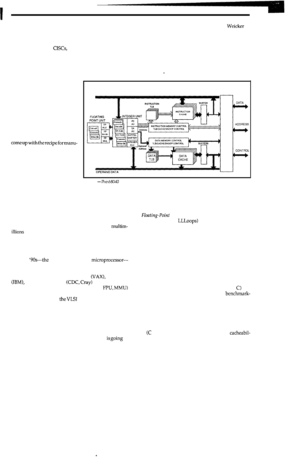
fear in the hearts of the RISC advocates. Notably, the RISC
Holy Grail of fewer clocks per instruction is challenged by
these clever CISC designs, as shown in Figure 3.
The RISC advocates wish Intel and Motorola would
quit making “good”
but they won’t.
Most are starting to recognize that, technologically,
the ‘ISC wars may not matter much. Integer performance
(where instruction set
complexity presumably matters) for
all the new chips is about the same and the main area for
An excellent presentation by Reinhold
of
Siemens (author of the Dhrystone benchmark) examined
the laundry list of popular benchmarks: MIPS (Native,
Peak, VAX), Whetstone, Linpack, Dhrystone, Lawrence
Livermore Loops, Stanford Small Programs Benchmark
Set, Quicksort, EDN, Spice, Sieve, Rhealstone, and SPEC.
Though widely used to “prove“ the superiority of one
chip or the other, these benchmarks, with the exception of
SPEC, generally suffer from one or both of the following
improvement is floating point. In the marketing sense of
problems.
pitting the aging gunfighters
against the new dudes, the ‘ISC
BUS
wars are still a big deal.
CONTROL
INSTRUCTION DATA
UNIT
TECHNOLOGY HEROES
The excitement over the
architectural merits of each CPU
is curious since the real heroes
are the process, fabrication, and
packaging technologists who
facturing theseever faster, denser
chips. While architects and de-
signers battle over 2x improve-
ments, those who actually manu-
facture thechipsmaydeliver 10x.
The big news for the ’90s is
that the increases in chip density
Figure 2
is the next step beyond the 68030.
and speed will continue un-
checked! The chip makers are prepared to challenge the
formerly conventional wisdom that the limits of VLSI are
right around the corner. Now, projections are that the
latest technologies (such as x-ray lithography) will carry us
into the next century before limits are reached.
In the ’90s you can expect to see goodies like:
l
150-MHz 64-bit CPU “modules” containing
of transistors.
*Viable, albeit “brute force” (not AI-based), voice
recognition technology.
l 16-Mbit and (near the end of the decade) 64-Mbit
DRAM technology.
The
third decade of the
will be marked by a power shift that will impact the entire
computer business. In the past, micro designers largely
followed in the footsteps of earlier mini
mainframe
and supercomputer
pioneers. Today,
having integrated all the pieces (CPU, cache,
onto single chips, the next steps are relatively uncharted.
From now on, it’s up to
chip designers to lead the
way to tomorrow’s computer designs.
BENCHMARKS LIE
It was generally agreed by all that benchmark hype
has reached the point of ludicrousness. Each claimant pro-
claims honorableintentions,butif theotherguy
to
lie, the temptation is to assume nice guys finish last.
Cacheability-Unfortunately, many of the most popu-
lar benchmarks (e.g., Whetstone and Dhrystone) are com-
posed of small routines and data sets which entirely fit in
the code/data caches of modern chips.
Fixation-Certain benchmarks (e.g.,
Whetstone, Linpack,
effectively measure only
one thing: floating point. This is fine for rocket scientists,
but of little relevance in most commercial applications.
System I/O performance (disk, screen, etc.) is never meas-
ured; doesn’t it matter?
Despite these limitations, the benchmarks could be
valuable if it weren’t for the chicanery of the suppliers. As
it stands, most of the claims are baloney. “MIPS” (Millions
of Instructions
Per
Second) is the worst offender, truly
being Meaningless Information Provided for Sales.
The other benchmark problems are related to “Apples
vs. Oranges” match-ups of system design (clock rate,
external cache size/speed), languages (Pascal vs.
and
compilers (supplier, optimization level, even
specific code generation). Together, these “fudge” factors
(especially compiler quality) far outweigh any true chip
performance difference.
SPEC-the System Performance Evaluation Coopera-
tive-is a group including Sun, MIPS, HP, and others
founded to come up with some real-world Unix bench-
marks compiler, SPICE, etc.) that address the
ity and floating-point fixation issues. Until then, buyer
beware!
February/March 1990
69
80386
MC68020
MC68040
LOAD
4
6
1
STORE 2
6
1
REG-REG 2
2
1
Figure 3
distinction between
and
is starting to
blur
as can seen by comparing the number of
clock cycles
used
per instruction between classic
processors and their
generation counterparts.
PCs VS. WORKSTATIONS
Much has been said of the impending collision be-
tween PCs and workstations somewhere in the
price range.
Hardware-wise, there is little differentiation between
a fully loaded personal computer (IBM/clone, Macintosh)
and the latest “personal” workstations from Sun, DEC,
Tektronix, and Data General. Whether PC or workstation,
the typical hot box has the following specs:
32-bit
MB RAM
*Various CRT options
*SCSI
*Ethernet
*Mouse
The claims of PC and workstation suppliers pretty
much evolve into the RISC/CISC battle; for now, PCs use
CISC (‘86,
while workstations use RISC (anything
else).
The important differences between PCs and worksta-
tions-those that really matter in the upcoming desktop
market-share war-aren’t technical. They are:
*Workstations run Unix, PCs usually don’t.
l
PCs
are sold via retail storesand mail order, worksta-
tions aren’t.
For now, despite technical and price/performance
similarities, these differences mean PCs and workstations
remain fundamentally different products. Who will be
first to bridge the gap?
SUPERCONTROLLERS
The Microprocessor Forum has a high-end focus.
Needless to say, there was nary an 8-bit controller to be
seen. However, conceding the existence of non-Unix,
desktop applications, a session was held on the
linechips intended for embedded applications. Naturally,
these supercharged chips are a far cry from the 4-bit job in
a toaster. They feature all the
of their desktop
CPU brethren, and more..
chip probably is the fastest piece
of silicon you can lay your hands on.
[Editor’s Note: For a
more detailed lookaf the 80960, see “Silicon Update” in
Small-Compufer Specialists
l
20-MHz 80386
l
1 MB RAM (expandable to 16 MB)
l
Shadow RAM Caching
l
65MB Hard Disk
l
5.25”
or
3.5” Floppy Disk
l
power supply
l
socket
l
Hercules-compatible mono graphics w/hi-res amber monitor
l
KeyTronic Enhanced
keyboard
l
Scores 22.5 on Norton 26 MHz on Landmark
MS-DOS.
Xenix, and Novell Compatible
Call for pricing and delivery
l
MHz 80286
. 512K RAM (expandable to 4MB)
l
32MB Hard Disk
l
5.25” or
3.5” Floppy Disk
l
200-watt power supply
l
80287 socket
l
Hercules-compatible mono graphics
w/hi-res amber monitor
l
KeyTronic Enhanced
keyboard
l
Scores 13.7 on Norton 16 MHz on Landmark
MS-DOS.
Xenix, and Novell Compatible
Call for pricing and delivery
MS-DOS 4.1 included with all systems. All TARDIS SYSTEMS
computers come with our fast service, 6-month parts and
labor warraniy, and exclusive
Upgrade Guarantee.
Call
or circle
155 on
the Reader Service Card
for complete custom system pricing and availability.
TARDIS SYSTEMS
945 San lldefonso Suite 15
l
Los
NM 87544
l
803865X
l
RAM (expandable to
l
65MB Hard Disk
l
5.25” or
3.5” Floppy Disk
power supply
socket
l
Hercules-compatible mono graphics
w/hi-res amber monitor
l
KeyTronic Enhanced
keyboard
l
Scores 18.0 on Norton SI; 20 MHz on Landmark
MSDOS,
Xenix, and Novell Compatible
Call for pricing and delivery
Service
70
INK
C
ELLAR
INK
Intel calls it
which boils migrate into broader markets. Remember, today‘s “high
down to executing multiple instructions in a single clock. end” is tomorrow’s “low end.”
AMD
desktop heritage of this
marketed” Unix CPU shows, but shouldn’t detract from RIDING IT OUT
the good points: 3-bus (instruction, data, address) archi-
tecture, register banks/stack cache, branch prediction.
Like a 7.1, the earthshaking chips of the ’90s aren’t the
a single-chip
outside
technological BIG ONE. Perhaps AI, superconductors,
gram ROM/EPROM is still required. The ALU is based on cold fusion, or another “fundamental” breakthrough will
the 32-bit ‘020, but the external data bus is 16 bits. Includes
render them insignificant. Nevertheless, I’m sure we can
2K bytes RAM, glue logic (chip selects), serial I/O, fancy all find good uses for a few million extra transistors.
X-channel timer, and a clever clock/power control scheme.
Now, if they could only figure out a way to make the
What took them so long?
darn things easier to program..
VLSI
CPU owes its heritage to Acorn
Computer (UK). Despite being originally designed for a
desktop machine, the 32-bit chip has a unique feature
desired in control applications: low cost. Not only is this
truly reduced RISC tiny (27,000 transistors), but it is also
designed to hook with “slow” outside memory chips (i.e.,
DRAM
S
), reducing system cost.
The good news is these puppies are quite fast (claimed
Microprocessor Forum and Microprocessor Report
Resources, Inc.
550 California Ave., Suite 320
Palo Alto, CA 94306
(415)
performance in marketspeak of 10 to 100 MIPS). The bad
news is that most are expensive. Also, many still carry
Tom
an M.B.A. from UCLA. He owns Microfuture,
necessary desktop/Unix architectural baggage (i.e.,
Inc.,
and kas been in Silicon Valley for 10 years involved in chip,
board, and system design and marketing.
tual memory, MMU, cache strategy, etc.) that may help
few, and actually hinder many, control applications.
IRS
For now, the
are confined to the
222
Very Useful
more expensive and esoteric end of the application
223
Moderately Useful
trum. Inevitably they, and future variants, will begin to
224
Not Useful
Photovoltaics for remote and online power
applications. Reliable, renewable electricity
from sunlight. Where there is a battery to be
charged, there is a place for photovoltaics.
RD4 Box 808
River Road
Brattleboro, Vermont 05301
802-257-1482
or circle 153 on the Reader Service Card
The PROM KING emulates EPROMS.
both
and money
your development
cycle Programmable seconds
your PC
port or any computer RS232 port. can
emulate most
devices.
8-256
downloads
High speed download:
expandable:
RS232
-4 EPROMS per
-PC
port
-Up to 8
Menu
software
Also programs
Battery backup
a real EPROM
$599 for 150nS
256K bits
Ask for pricing of other options
Made USA by.
Reader
157
February/March 1990
7
1
Memory Management
on the HD64180
SOFTWARE
BY
DESIGN
Jack Ganssle
t seems that most of C
IRCUIT
C
ELLAR
INK’s readers develop embedded
code on and
microproces-
sors, However, many of the most com-
mon 8-bit architectures are based on
rather ancient designs. The venerable
is nearly
old,
yet continues
to dominate the 8-bit market.
72
CELLAR INK
While B-bit technology has remained fairly stable,
applications have not. In the
a microprocessor-based
(product just had to offer bare functionality to be a success;
Products seem to have to offer virtually every conceivable
function, since management and the customer see the
creasedperformanceasrequiring”onlyasoftwarechange.”
Developing solutions to these more complex prob-
lems
bigger programs and the corresponding
extra address space. In addition, the cost of developing
software is forcing most companies to use high-level lan-
guages. While most proponents claim C is only about
less efficient than assembly, extra memory must
indeed be available. Finally, the decreasing cost of mem-
ory makes more complex problems manageable; as mem-
ory costs decrease, you can be sure that someone will find
a need for even more!
Traditionally,
computers have been touted as
the solution for memory woes. Certainly the 68000, with
a huge linear address space, offers a great way to take
advantage of large DRAM
S
. Those of us working in the
controller world frequently can’t use these more powerful
often we want to simply upgrade an old application
based on an B-bit CPU.
Hitachi introduced the HD64180 as a high-integration
replacement. One of its most important features is the
memory management unit. In my informal surveys, I have
found that while the on-board I/O is a requirement of
many applications, the MMU is the primary decision
factor for many engineers who select the chip.
The chip offers a memory management unit designed
to let B-bit applications break though the artificial bounds
of a 64K address space. It doesn’t automatically handle the
extended memory.
This, then, is the
problem you face when electing to use
an B-bit CPU cum MMU rather than a processor with an
intrinsically large address space. It can be tedious and
troublesome to take advantage of the MMU. In most cases,
it is impossible to come up with a scheme to casually hop
all over memory; crucial to the successful use of the MMU
is a partitioning of the application to work comfortably
within the
restrictions.
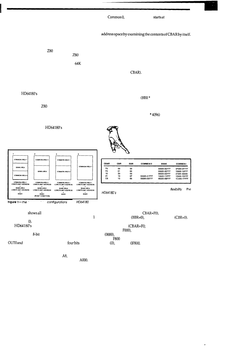
LOGICAL VS. PHYSICAL
It is important to understand the concept of logical
versus physical addresses. Physical refers to the proces-
sor’s actual address range: 1 MB on the HD64180. Physical
addresses are applied by the hardware to the memory de-
vices. Logical addresses are issued by your program.
Again, on the HD64180 the logical addresses arelimited to
the same 16 bits that the
used for addressing; logical
addresses can never exceed 64K. The
has 64K of
logical and physical address space; the two are one and the
same. The HD64180 gives you the same
of logical
space, but 1 MB of physical space. The function of the
MMU is to translate the logical addresses used within your
program to physical addresses that are
sent to memory.
On the HD64180, the MMU is a hardware device built
onto the processor’s silicon. Every non-DMA memory
address is translated by the MMU from 16 to 20 bits.
The
MMU uses three internal control reg-
isters. In keeping with the chip’s design philosophy, on
reset the MMU gives a straight logical-to-physical map-
ping, simulating the
and, of course, limiting the ad-
dress space to 64K.
MMU REGISTERS
You
can divide the
logical address space
into one, two, or three areas. The logical space itself is
unaltered; even when divided it is still a contiguous 64K.
This process defines how each of the (up to three) areas
exists in physical memory.
Tour
possible
of the
MMU
allow one. two. or
three logical partitions.
Figure 1
of the possibleconfigurations. Note
that each is associated with a rule (e.g., Common Area
=
Bank Area = This rule is a condition programmed into
the
CBAR register, and is what you use to
define the logical limits of the address space.
CBAR is an
I/O port (though most users refer to
it as a register) that can be accessed by the processor’s
IN0 instructions. The lower
specify the
starting address of the bank area, and the upper four give
the start of common 1. These bits determine the upper four
bits of the address. If CBAR were
then the base area
starts at 8000 logical, and common 1 starts at
if it exists, always
logical 0000 and
runs up to the bank area. The bank area then runs to the
start of common 1.
Therefore, you can always understand the logical
No other information is needed. Figure 1 is a quick “cheat
sheet” giving the possible configurations.
The logical address is only part of the problem. How
does logical space get mapped to physical? Two other
registers (actually, I/O ports) provide the rest of the an-
swer.
BBR (the Base Bank Register) specifies the starting
physical address of the base area (remember, the logical
start was given in
CBR (Common Bank Register)
provides the same information for common 1. Both of
these specify the upper 8 bits of the 20-bit physical address.
A simple formula gives the translation from logical to
physical address for the bank area:
Physical = Logical +
4096)
The same formula gives Common 1:
Physical = Logical + (CBR
BBR and CBR gives the upper
eight address bit only-hence the
4096 multiplier. The lower 12 bits
come from the logical address.
Thus, the translation only really
affects the upper 8 bits; the lower
12 physical bits are always identi-
cal to the lower 12 logical.
Table 1 -Some
examples ofhowthe logicalacfdressspace can be
mapped onto thephysicaladdressspaceshow the
of
MMU.
On reset, the HD64180 sets CBAR to FO, and
CBR=BBR=O. This maps logical to physical exactly, with
no translation; the bank area starts at logical 0000 and
common 1 at FOOO (since
the bank area physi-
cally starts at 0000
as does common 1
If
logical address 1000 is generated, the MMU allocates this
to the bank area
1000 is less than the start of
common 1 at
and adds the physical base of bank to
it
giving a translated address of 01000. Similarly,
logical
is in common 1, and is translated by adding
CBR yielding
Table 1 shows some more ex-
amples.
By now it is pretty clear that while the MMU is not all
that difficult to use, it does require a lot of thought.
Admittedly, with only a few instructions you can set up
February/March 1990 73
any mapping. This does not mean that a casual approach
will yield a I-MB linear address space, since every time the
program transfers control over a map boundary the map-
ping registers must be reset manually. That is, jumps and
calls within a large program potentially require remap
ping.
Few HD64180 users successfully use the MMU to
write huge programs without completely restructuring
the program’s design. The key to the MMU is careful
partitioning of the problem.
In most embedded systems, either the program or the
data structures are so large that they require the
services. In some pathological cases both might be a
problem. Examine the problem first; design a solution
based on the program’s real needs.
THE DATA PROBLEM
Accessing large data structures can be an almost in-
tractable task. When writing an assembly program, it is
common to search and initialize arrays by pointing HL or
the index registers to the base of the variable and incre-
mentally manipulating each location. If the array cannot
fit in the processor’s logical address space, then the MMU
can indeed be used to access it, but whenever the memory
pointer is incremented, a test must be made to see if a
remap is needed. This isn’t hard, but it can be very slow.
If you are working with one or more large arrays,
divide the map into two or three segments, and assign one
of these to the array structure. Generally, another would
be used to access the ROM, and the third to handle pro-
gram temporaries (miscellaneous variables needed in
RAM). The area of the logical map assigned to the array
is then a virtual window into the data; at any time
4K of the data is available, and
by
changing
the
CBR
value other 4K segments can be used.
It’s
usually a
bad idea to
write
code that directly works
on the array. Isolate the entire data structure from the
application program by using a driver to access it. The
hardware-dependent aspects of MMU management are
then buried in one easily maintained subroutine.
Be very careful when handling interrupts with this (or
any memory management) scheme. Since the interrupts
are by their very nature asynchronous, the interrupt serv-
ice routine can gain control with any of a number of maps
set. If the ISR needs access to the data, some mechanism
must ensure that the MMU is set properly. Be especially
sure that the stack is restored before the
is executed.
CODE MANAGEMENT
manager is the promise of using large programs. Yes, it is
possible to write huge monolithic programs that crudely
simulate a more or less linear address space via the MMU.
However, this is not advisable unless using a high-level
language that can automatically manage the details.
Every experienced programmer divides a complex
program into many small functions. This top-down de-
composition
combined with careful grouping of the
functions into modules that can share identical logical
address space to minimize remapping.
The three-space memory model is the best for han-
dling big programs. Common 0, located at physical ad-
dress 00000, is never remapped. It contains the interrupt
service routines and all other commonly invoked code.
The system’s “main loop” typically also resides here.
Common 1, which occupies the end of the logical
address space, is mapped to the system’s RAM, and holds
all of the program’s variables. It may be remapped, but
only at great peril, since the stack will certainly be lost.
The base area, sandwiched between the two common
blocks, is where most of the remapping activity takes
place. Perhaps the bank area is only 4K long; functions can
be grouped
together until 4K worth has been accumulated,
and this group compiled at the logical address assigned to
the bank area. Each group is compiled at this same
address, and then loaded into different physical segments.
(Assembly programmers might use the PHASE and
DEPHASE pseudo ops to create these virtual overlays).
A driver routine in common 0 is used to invoke each
function; no calls are made between functions without
going through the driver. It remaps the MMU as needed
every time a function call is made, and then branches to the
proper routine.
This approach has a profound benefit. New maps can
be selected by reloading just the BBR register. Obviously,
this is faster than resetting a complete, complex new map.
Even better, the memory management unit is always in a
good state; a partial map is never loaded and interrupts
can be left on while remapping. A BBR value can be
associated with each function, as well as a starting address
within the bank area, making function invocation easy.
This is the approach taken in the real-time operating
system I described some months ago. [Editor’s Note:
two-part article “Writing a Real-Time Operating
System”
appeared in
C
IRCUIT
C
ELLAR
INK
issues 7 and 8.1 The
tasks are each loaded in the bank area. The context
switcher, once all normal operating system activities are
done, simply reloads BBR before vectoring to the next task.
This approach is by no means intended to be all
inclusive; it somewhat precludes the use of both large
RAM and ROM spaces. It does
help
organize
big
programs
in a useful, maintainable fashion.
It seems silly that this tedium can’t be taken over by a
smart programmer’s assistant. Some C compilers do
support automatic management of the MMU. In assembly
you’re on your own. Softools (P.O. Box 2412, Columbia,
MD 21045) sells an assembler/linker that lets you divide a
program into modules that are all mapped as virtual
overlays. The linker generates the code needed to drive the
MMU whenever a “long” call is coded. The software also
generates source-level debugging information so that an
emulator can track the code in each of the different maps.
SPECIFIC PERILS
The MMU is guaranteed to cause lots of problems if a
few rules are not followed. Unfortunately, it seems that
most programmers acquire this knowledge through bitter
experience.
As I suggested above, it is usually a good idea to keep
a small kernel mapped in low memory all of the time.
Remap the MMU by calling this driver. Otherwise, your
program might accidently map itself out-the routine
doing the remap could get lost when the MMU I/O load
instruction is executed! While in certain rare instances this
can be useful, it should generally be avoided.
Of course, if you call a routine in the kernel to do a
remap, be sure the return address remains mapped in.
This certainly applies to the stack as well!
It is crucial to carefully plan each and every load of the
MMU registers. Since three registers are needed to define
the complete memory configuration, the order in which
the mapping registers are loaded is important. In other
words, you might map your code out when simply trying
to change data access areas. Sometimes CBAR should be
loaded first; other times the BBR and CBR registers. In all
cases, examine the code to ensure that at each step of the
mapping process the program doesn’t get mapped out.
A related and extremely common problem is setting
the MMU registers with data loaded from RAM. If each
read from
memory
and
then output to the memory
manager, you’ll frequently map out the RAM from which
the mapping values are being read in one of the interme-
diate steps.
Finally, interrupt-driven systems must be carefully
designed so the stack is always available, and so the
interrupt service routines are always visible. Further,
when in the process of loading the registers, an interrupt
that comes when the MMU is partially set up can be a
disaster. Usually it is a good idea to disable interrupts
before changing the MMU parameters.
SOME
THINGS CHANGE
There are as many different ways of handling a mem-
ory management unit as there are programmers. All
involve careful analysis of the problem, and selection of a
memory configuration matched to the
In many cases, a substantial
to the program’s structure may be
in order.+
IRS
processordevelopment tools. When not
electronsaround,
upanddown
Coast
on his 35-foot sloop.
225
Very Useful
226 Moderately Useful
227 Not Useful
IN-CIRCUIT EMULATOR
is a low-cost real time emula-
tor
for the Motorola
family of single chip
microcomputers. Any host computer with serial
pot-l and terminal emulation software can be used
with TECICE-HC05. Base price is
Complete development system software is avail-
able for MS-DOS computers including the Byte
Craft Limited
Code Development System
which includes a 6805 C compiler with Integrated
Development Environment.
BOX 8C
l
Barton, Vermont
05822
Phone
525-3458
l
Fax
525-3451
E/EPROM MICRO
PROGRAMMER
Regular
Special
Offer
$395
VISA ACCEPTED
MICRO-BURNER System
512
The MICRO-BURNER sets a new price performance stan-
dard
in programmers adaptable to all single-chip micros
with on-chip EPROM. Features include reverse EPROM
detection/protection and 12 volts DC operation for port-
able applications.
money-back offer.
USA Distributor
CANADIAN Distributor
QUALTEK Corp.
Products Ltd.
Lynwood, WA
North Vancouver, B.C.
(206) 742-l 777
(604) 988-9853
February/March
75
Excerpts from the Circuit Cellar BBS
TIME
The Circuit Cellar BBS
bps
24 hours/7 days a week
871-1988
Four incoming Lines
Vernon, Connecticut
In this insfallment of
we’ll be covering how
to detect leaky pipes, and how to make real short pulses.
First, though, with the current popularity
of fax
machines
especially fax expansion boards for PCs, the issue of
how to turn the computer on fast enough to catch the
incoming call becomes important, as we find out in
discussion.
From: DAVID WILLIAMS, SR. To: STEVE CIARCIA
I’ve installed a fax board in my IBM AT clone. Keeping the
computer on all the time is a pain. Do you know of a manufac-
turer who makes an auto-on switch that will boot up the com-
puter when the fax line rings?
From: JEFF BACHIOCHI To: DAVID WILLIAMS, SR.
Considering the amount of time it takes to power-up a system
and run an application program, most fax machines will give up
long before you get anywhere near answering the phone. The
best you could hope for would be a call-back within x-minutes!
From: NATHAN ENGLE To: DAVID WILLIAMS, SR.
I have to agree with Jeff about fax machines giving up before your
machine gets booted up. It’s a race you’re practically guaranteed
to lose, and I can’t really see the fax board manufacturer feeling
too happy about it either. You’re not leaving very much time for
their card to get to the call once you’re done booting.
I used to feel very much like you did about leaving the PC turned
on all the time; I have been doing it for the past year, though, and
I’ve noticed
no
increase in my bills. The power supply
in an XT is usually 130 watts; about what a light bulb takes, right?
From: JEFF BACHIOCHI To: NATHAN ENGLE
The monitor can be switched off with the machine still running.
It is the start-up and thermal cycling that deteriorates
nents at a faster rate than leaving them on full time. Remember
the power supply rating is a maximum, your system may in fact
draw much less (pennies a day).
From: NATHAN ENGLE To: JEFF BACHIOCHI
That’s a good point; I think the way my XT is loaded I come in
near the upper end for power usage.
I have been leaving my monitor on since have one of those
VGA cards that has a built-in screen saver function. This is
available in shareware for people with other kinds of displays.
From: DAVID SMITH To: NATHAN ENGLE
On the subject of leaving a monitor on for extended periods of
time, I don‘t think it would be advisable since the screen saver
function just shuts off the video but does not turn off the filament
in the picture tube. When a filament or heater in a CRT wears out
in a TV set they rejuvenate it; but it can only be rejuvenated once
or twice.
Jameco does sell a fax board that will turn on your
computer (Niche Tek,
but I agree with leaving your
computer on (but not the monitor).
From: JOHN
To: DAVID SMITH
Can the monitor be at all damaged by having the constant input
from the system while
it’s
off. I’ve considered turning off my PCS
Ultrasync off during overnight jobs, but have been scared to for
that reason. I do use PC Mag’s VGA Dimmer, though.
From: NEIL CHERRY To: JOHN
My understanding is that when off you’ll do no damage. But it
may be possible to “blank” the screen. On Hercules graphics
cards you simply switch a bit and the screen goes off. I believe
that the EGA and VGA both have the same capabilities. This
would be equivalent to turning off the monitor.
While many
of us
wouldn’t think electronics had any ap-
plication in
thefollowing thread shows
how wrong that thinking is.
From: DANIEL L. MILLER To: PAUL HITCHCOCK
Is there a way to detect water leaks from pipes? Say about a
foot run of pipe through the attic. I want to automatically shut off
the water pump if a leak is detected. Surely someone in the
refinery industry has evolved some solutions to this type of
problem.
From: ED NISLEY To: DANIEL L. MILLER
How much of a leak?
If you’re looking for a torrent, measuring the pressure drop at
both ends of the pipe should give you a pretty good idea. You’d
have to calibrate the setup for the normal pressure drop at
whatever the usual flow rate is, but that’s a simple matter of
software.
If you’re looking for a trickle, that’s a different problem entirely
(and theonemost likely to occur, too!). Although I don’t thinkit’s
a standard technique, how about running a length of
insulated two-conductor cable around the pipe (a spiral wrap
with a few turns per foot) and measuring the resistance between
the conductors? Put a resistor on the far end and you’d have
built-in detection for open circuits, too!
pipeleaks I’ve had to contend with were pretty obvious,
so the only detector technology I needed was an eyeball. Oh
well...
From: PAUL HITCHCOCK To: DANIEL L. MILLER
Well, I don’t know about detecting leaks in long lengths of pipe
(especially cold water pipes which sweat), but near joints I have
used two coils of wire, separated by a
dry
cotton pad which I had
previously soak in salt water before drying. For a large leak
(which is what I was looking
the resistance change (infinite
to finite) was fairly dramatic as I recall. It’s been a number of
years since I tried this trick, and I don’t remember exactly how
much wire I used.
From: DANIEL L. MILLER To: PAUL HITCHCOCK
Thank you.
My
air conditioning system uses water to cool the
house heat pump coils. The water source is a source well and the
drain is an injection well. It pumps 32 gpm and I tend to get
nervous thinking about that circulating through PVC pipe that is
too small in diameter and shudders whenever the units switch on
and off,
From: ED NISLEY To: DANIEL L. MILLER
Run, do not walk, to your nearby plumbing supply store and get
some straps to secure that pipe! It will eventually crack the
fittings (not the glued connections) or the pipe sections that are
taking the most strain and
hell will break loose.
If it’s shaking that much, you may
need
a standpipe (closed at the
top) to act as a shock absorber-the same sort of thing plumbers
delight in putting inside a wall at the end of a long run. After a
while the air is absorbed, the standpipe fills up, and you’re back
to a colossal water hammer banging in your walls..
have to
rip the wall apart to drain the standpipe unless they did a very
good job of sloping the pipes.
From: PAUL HITCHCOCK To: DANIEL L. MILLER
Dan, I read Ed’s
reply and
completely
agree:
STRAP that pipe! At
the flow rate you’re talking about, a sustained waterhammer
incident can put immense stress on both the pipe itself as well as
the joints. (The thought of 32 gallons flowing into the attic every
minute makes me shudder!) The stand
pipe
is a good idea as well
and you might even consider encasing the PVC within a length
of steel gas pipe.
Without detailed
knowledge
of
your plumbing, my best idea is to
install flowmeters at each end of the pipe (both downstream from
the standpipe) and hook up a controller that shuts off the pump
whenever a certain differential flow rate occurs.
Omega Engineering (One Omega Drive, Box 4047, Stamford,
06907-0047) carries an extensive line of flowmeters. I understand
however. Maybesomebodycanpoint
you in a less costly direction.
From: DANIEL L. MILLER To: ED NISLEY
Thanks. As soon as I moved in I did what you said and added
antiwaterhammer devices. These are small tubes charged with
nitrogen with a neoprene bladder that doesn’t deflate with time
and adds capacitance (i.e., they work similar to the
filter
capacitor
inapowersupplyandaremuchsmallerthanstandpipes).
have sustained knock but do have turn-on/turn-off transients. I
think I’m going to call a plumber and put the main connection
pipe outside underground where it belongs and get it out of my
attic! Thanks much for help.
From: FOSTER SCHUCKER To: DANIEL L. MILLER
In the August 1989 issue of Industrial Equipment News, there is
aarticleabout
system. You wrap this
fancy cable around or along your pipe and it tells you
when and
where it leaks. Contact: Raychem Corp., 300 Constitution Dr.,
Menlo Park, CA 94025. It’s called
500. Good luck!
February/March 1990
7 7
There are numerous methods that can be used to generate
individual pulses on the order of several microseconds and
longer,
but ve
pulses can
be
difficult to come by, as
we see here.
From: TOM CARTER To: ALL USERS
I would like to know a good way to generate a pulse under 100
ns wide using easy-to-get
or CMOS or whatever. A pulse of
50 ns or shorter would be best. Thank you for any help.
From: NATHAN ENGLE To: TOM CARTER
Do you want to get individual pulses that are that wide? Or
asking another way, would a
waveform do?
If you’ve got a really short trigger
you
want to stretch, then
you can use an
or any of the “multivibrator” class of chips.
These chips should really just be called “pulse stretchers.”
If you need single pulses, I think the ‘221 may do that for you the
best. They work kind of like 555 timer chips: you get to play
around with an external capacitor and resistor to get the timing
you need. Then you trigger your pulse with an edge transition.
Any help?
From: TOM CARTER To: NATHAN ENGLE
I want single pulses that are triggered by a rising or falling edge
(rising only or falling only). I have seen circuits like I need using
a 74121 with a
capacitor and
resistor which gener-
ate
pulses. I guess I need to know how small I can make
the values and still get a good pulse. Under 50 ns is what would
really like.
Steve Ciarcia has assembled a team of engineers,
designers, and programmers to produce the products
that have made Circuit Cellar famous. Now you can put
the Ciarcia team to work for you.
Steve Ciarcia and his staff have designed products
ranging from communications and networking compo-
nents to multiprocessing computers. Current capabili-
ties include every phase of design and production, from
initialconceptthroughpackagingofthefinishedproduct.
Whether you need an on-time solution for a unique
problem, complete support for a startup venture, or
experienced design consulting for a Fortune 500 com-
pany, the Ciarcia Design Works stand
you.
Remember.. .a Ciarcia design works!
From: ED NISLEY To: TOM CARTER
If you’re really interested in good, clean, tidy pulses under 50 ns
wide, you need to be careful about which logic family you’re
using. The rise time and fall time (which are
usually the
same) are a significant part of your total pulse width, so you‘ll
have to pick a set of gates that work in your application.
You can use a NAND gate to generate quite nice pulses if you set
up a deliberate race condition: feed both inputs from the same
source, but one input goes through an odd number of inverters.
When the sourcegoes from high to low, you get a negative output
pulse as long as it takes the signal to propagate through the
inverters. Other logic gates will give you different triggering
conditions if you need them.
You can trim down a pulse by inserting pairs of inverters; each
pair will shave a few nanoseconds off the leading and trailing
edges of the incoming pulse.
The only catch with all this is sensitivity to things like tempera-
ture, supply voltage, the phase of the moon, and so forth. You
will
a fine oscilloscope to verify what’s happening; the
more bandwidth the better, because you’re interested in the
width of a pulse that’s almost not there!
The Circuit Cellar BBS runs on a
Micromint
OEM-286 IBM PC/AT-compatible computer using the
multiline version of The Bread Board System
and currently has four modems connected. We
invite you to call and exchange ideas with
Circuit
Cellar readers. is available 24 hours a day and can be
reached at
8
dnta bits,
stop bit, and either
or 2400 bps.
IRS
228
Very Useful
229 Moderately Useful
230 Not Useful
SOFTWARE
and
BBS AVAILABLE on DISK
Software
on
Disk
Software for the articles in this issue of Circuit Cellar INK may be downloaded free
of charge from the Circuit Cellar BBS. For those unable to download files, they are
also available on one
5.25” IBM PC-format disk for only $12.
Circuit Cellar BBS
Disk
Every month, hundreds of information-filled messages are posted on the Circuit
Cellar BBS by people from all walks of life. For those who can’t log on as often as
they’d like, the text of the public message areas is available on disk in two-month
installments. Each installment comes on three
5.25” IBM PC-format disks
and costs just $15. The installment for this issue of INK (February/March 1990)
includes all public messages posted during November and December, 1989.
To order either Software on Disk or Circuit Cellar BBS on Disk, send check or
money order to:
Circuit Cellar INK Software (or BBS) on
Disk
P.O. Box 772,
Vernon, CT
or use your
or Visa and call (203) 875-2199. Be sure to specify the
issue number of each disk you order.
7 8
CIRCUIT CELLAR
STEVE’S
OWN
An Analog State of Mind
INK
Sieve
he last time I wrote one of these pages, I was talking
about fixing a high-tech German car
using a two by four.
This time around, you’re going to read a short lesson on
digital overkill. Now don’t get me wrong: I’m still in favor
of computer solutions to many problems, and the idea of
high-powered computing toys still turns me on. I’ve just
spent a lot of time lately hearing people moan about
problems they’ve created for themselves by using too
much technology for the problem, and it’s starting to get
on my nerves.
Let’s start with the obvious. I’ve never made any
secret of the fact that I much prefer working with digital
circuits to trying to figure out analog. As far as I’m
concerned, the world would be a much easier place to
work if I didn’t have to worry about analog at all. I’m not
alone here-most digital electronics engineers have fanta-
sies about a purely digital world. Most of us realize,
though, that at some point in the process, you’re going to
have to bite the analog bullet if you want a working,
world application. The problem is with the people who
say that they’re going to design an analog section (under
protest, of course) but who try to cut intellectual comers by
keeping their digital
One of the most frequent mistakes
I see
is caused by
folks holding on to a mistaken notion of accuracy. When
we’re talking about accuracy in a digital sense, I’ve found
that most engineers run out of interest
long before they run
out of bits. Since all of those oh-so-accurate bits are there,
computer designers have gotten used to the idea that you
run your answer out to as many digits as you have avail-
able. Leaving aside the question of whether anyone really
needs to (for example) balance their checkbook down to a
millionth of a cent, the result of all this has been a redefini-
tion of how much accuracy is acceptable.
Back
in the days
of the slide rule, when dinosaurs roamed the earth, two
digits to the right of the decimal point was acceptable for
most purposes, and four places meant that you had done
some
serious work. Now that a four-dollar calculator can
better that accuracy for simple function, some people
forget that there are a lot of instances
where you just can’t
demand accuracy down to a gnat’s eyelash.
I’ve had to learn to accept some “creative looseness”
when it comes to dealing with analog signals.
When I let
myself get into an analog state of mind, I realized that there
were places where the quest for accuracy turned around to
bite me. If I’m working on a climate-control automation
system for my
house, I can demand that the input section
be accurate down to a tenth of a degree, and I can set action
points to that accuracy. The sensors are available, and the
microcontrollers can certainly handle the bits. The trouble
is, the extra accuracy requires three extra weeks of work,
can lead to unpredictable operation of the system, and just
isn’t necessary. If I were to press for the added accuracy,
I’d just be rewarded with aggravation and failure for my
efforts. The fact is that single-degree accuracy is finer than
most humans can discriminate, so it’s certainly accurate
enough for the job.
It’s all a matter of using the right tool for the job. I
don’t use a hammer when I want to tighten a bolt, and I
don’t try to make the analog part of a project work in ways
that are contrary to reality.
C
IRCUIT
C
ELLAR
INK
concen-
trates on the digital end of the process, but there’s no way
that
any
engineer can hope to build successful applications
that interface with the real world without knowing the
analog. Taking the time to learn makes a hacker into a real
engineer, and keeps you from reaching for a pair of pliers
when a hammer is what you need.
80
Wyszukiwarka
Podobne podstrony:
circuit cellar1991 02,03
circuit cellar1992 02,03
circuit cellar1994 02
circuit cellar2000 02
circuit cellar1995 02
circuit cellar1994 02
circuit cellar2003 02
circuit cellar2004 02
circuit cellar2002 02
circuit cellar1993 02
circuit cellar1997 02
circuit cellar2001 02
circuit cellar1996 02
circuit cellar2000 02
circuit cellar1993 02
circuit c
więcej podobnych podstron