
2
Microfluidics Meets Nano :
Lab-on-a-Chip Devices and their Potential for Nanobiotechnology
Holger Bartos, Friedrich Goetz, and Ralf-Peter Peters
2.1
Introduction
Microfluidic devices and integrated chemical measurement systems were among the first
ideas when the investigation of nonmicroelectronic applications of microfabrication technol-
ogy was started more than two decades ago. In 1979, an integrated gas chromatograph was
fabricated on a 2-inch (5-cm) silicon wafer [1]. Concepts and first applications of miniaturized
total analysis systems emerged in 1990 [2]. During the past decade, array technologies and
microfluidics have become commercially available in biochips for genomics and proteomics.
It is expected that many more applications will appear on the market in the near future, as
these devices are presently under development in many companies world-wide.
It should be noted that the structures used in microfluidic and in Lab-on-a-Chip devices
are not nanostructures, but are in the micrometer to even millimeter range. However, bio-
nanotechnology requires a microfluidic platform technology as an interface to the macro-
world : for self-assembled monolayers; for the handling of nanoparticles, cells or nanobar-
codes; and to monitor and control cellular machinery.
On the other hand, nanobiotechnology will enable novel microfluidic platforms due to
the integration of nanostructures, nanocoatings or nanoactuators, by the integration of
nanoporous membranes, and by integrating detection and measurement techniques
such as nanoelectrodes, nanooptics, and patch–clamp arrays.
2.2
Overview
2.2.1
Definition and History
A microfluidic chip is defined as an assembly of microstructures on a common substrate,
used for the manipulation of fluids (gases and/or liquids).
A Lab-on-a-Chip device is a combination and integration of fluidic elements, sensor
components and detection elements to perform the complete sequence of a chemical
13
Nanobiotechnology. Edited by Christof Niemeyer, Chad Mirkin
Copyright
c 2004 WILEY-VCH Verlag GmbH & Co. K aA, Weinheim
ISBN 3-527-30658-7
G

reaction or analysis, including sample preparation, reactions, separation, and detection.
This chapter focuses on Lab-on-a-Chip devices for Life Science applications, and does
not cover microreactors for chemical synthesis [3].
Both, microfluidic as well as Lab-on-a-Chip devices, were part of the vision when micro-
fabrication technology – which had emerged from the fabrication tools for microelectronic
devices – was first applied to problems in mechanics, optics, and fluidics. Among the first
examples were a gas chromatograph developed at Stanford University [1], and pioneering
work on inkjet printheads at IBM in the late 1970s [4]. The inkjet printhead has become
one of the commercially most successful fluidic applications of this new technology,
which was called “MEMS” (Micro Electro Mechanical Systems) in the U. S. and
“Microsystem Technology” in Europe.
Many discrete microfluidic devices, such as microvalves [5], micropumps [6, 7], flow
sensors [8], and chemical and biological sensors [9] were developed, but the benefits of
miniaturization are best taken advantage of when these devices are integrated into a
fluidic system. Intensive work on Lab-on-a-Chip systems was started in the early 1990s
[10–12], and today integrated microfluidic devices are established in laboratory equipment
for biomedical research and starting to penetrate the diagnostic market for point-of-care
and laboratory automation applications.
2.2.2
Advantages of Microfluidic Devices
Microfluidics offer advantages both from a technical as well as from an economical view-
point. When the dimension of fluidic structures are scaled down to the micrometer re-
gion, the surface to volume ratio of the fluids involved increases dramatically, and surface
effects start to dominate volume effects. For the fluid flow in microstructures this leads to
well-defined flow characteristics, as the flow is strictly laminar and turbulence can only
appear in very limited regions around sharp edges.
Due to the absence of reasonable turbulence, mixing of different fluids can only be
achieved by diffusion, or by specially designed fluidic mixing elements. Moreover, due
to the scaling factors of diffusion and heat conduction, the equilibrium conditions can
be reached much faster.
The small sample volumes involved are of enormous advantage especially for highly
parallel applications, like array devices used in genomics, proteomics, and drug discovery.
The reduction in the amount of substance required for each reaction leads to significant
cost reductions for these types of applications. Another advantage associated with small
sample volumes is that minimally invasive methods are sufficient for taking samples,
for example of blood or interstitial fluids.
These small volumes can be precisely controlled by taking advantage of microfluidics.
In some cases, this is achieved just by a proper definition of the geometric dimensions
of the corresponding channels, wells, and reactors. Another method to define precisely
small fluid volumes is droplet generation; this is a separate application field of microflui-
dics, with important products such as inkjet printheads or drug delivery systems. Array
spotters are another product of this kind, used in the immobilization process of nucleic
acids, antibodies, etc., and will be described in section 2.3.5.
14
2 Microfluidics Meets Nano : Lab-on-a-Chip Devices and their Potential for Nanobiotechnology
The large surface implies a high reaction efficiency, as the surface areas which may be
coated with catalysts or enzymes are large compared to the reaction volume. Furthermore,
due to the large surface to volume ratio, capillary forces dominate volume forces such as
gravity, and may advantageously be used for fluid transport in single-use devices. Finally,
integration and the mass-fabrication capabilities of microfabrication technology make the
application of microfluidics economically attractive.
2.2.3
Concepts for Microfluidic Devices
For microfluidic chips, two main organization principles are used in integrating the
fluidic elements on the chip.
One principle is parallelization; this is used when the same type of reaction has to be
performed in parallel many times. Examples are array type of chips found in DNA anal-
ysis, proteomics and high-throughput screening. Parallelization can lead to dramatic cost
advantages in three ways : First, the manufacturing cost for a device with many integrated
reaction wells is much lower than that for many devices for just one reaction; second, all
reactions are performed in parallel, saving labor cost and time; and third, parallel reac-
tions are an ideal input for laboratory automation and information processing of the
assay results.
One very basic application of the parallelization principle are nanotiterplates, an exten-
sion of the well-established micro plate technology into the nanoliter region. A review of
nanotiterplates is given in Ref. [13].
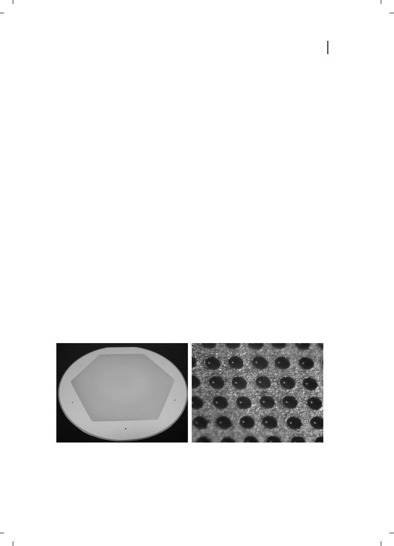
As an example of parallelization, an array of 250 mm
q 250 mm wide, 500 mm deep,
bottomless wells is shown in Figure 2.1. One chip will carry up to 100 000 of these rea-
ction wells. This Living Chip
TM
technology was developed at MIT and commercialized
by BioTrove, Inc.
The second basic organization principle is sequential integration. Here, several fluidic
structures, each designed to perform one step in a processing sequence, are integrated on
15
2.2 Overview
Figure 2.1
The 100K Living Chip
TM
plate (left) and a detail view of the 50-nl wells filled with liquid (right).
Massively parallel reactions may be initiated by stacking of chips; applications include drug discovery,
genomics, and proteomics. (Courtesy BioTrove, Inc.)

one substrate and interconnected by a channel network to provide the transport of the
fluids between the processing steps. The fluids will pass the processing steps in a sequen-
tial manner. The fluidic structures involved are channels, mixers, reaction chambers, de-
tection chambers, sample and waste reservoirs, microvalves, micropumps, microsensors,
heating zones, and many others; for a detailed description see section 2.3.2. Some of the
fluidic structures may also have electrical, mechanical, or optical functions and the corre-
sponding elements and interfaces; these may also be integrated into the microfluidic chip,
or added in a discrete way. In many cases, complete fluidic components, for example
micropumps, are added as discrete components to the microfluidic device. Recently,
attempts have been started to standardize such elements with respect to size and input/
output terminals, to create standard building blocks for modular fluidic devices [14].
One important example of sequential organization is that of micro Total Analysis Sys-
tems (mTAS). These are fluidic systems which are integrated on one substrate and are in-
tended to perform the total sequence of a chemical analysis, having been developed in sev-
eral laboratories worldwide [15, 16]. Recent results are found in the proceedings of the an-
nual conference on this topic [17]. A first application was an integrated system to monitor
the glucose content in a fermentation process [18]. Another, very important application for
microfluidic devices are PCR reactions [19, 20]. An example of a commercially available
system, which performs sequentially the preparation, amplification, and detection of
DNA, is described in Ref. [21].
The sequential organization scheme is also represented by capillary electrophoresis
chips [22] (see also Figure 2.5). With dielectrophoresis, cells and particles in a weak elec-
trolyte solution may be moved and collected using the forces induced by travelling, rotat-
ing, or alternating electrical fields; a review is given in Ref. [23].
Some microfluidic devices combine both organizational principles. Array-type fluidic
chips will, in most cases, require a channel network for fluid transport, and more complex
reaction sequences require more than one reaction site. On the other hand, in most cases
it is favorable to include parallel processing in sequential arrangements. A combination
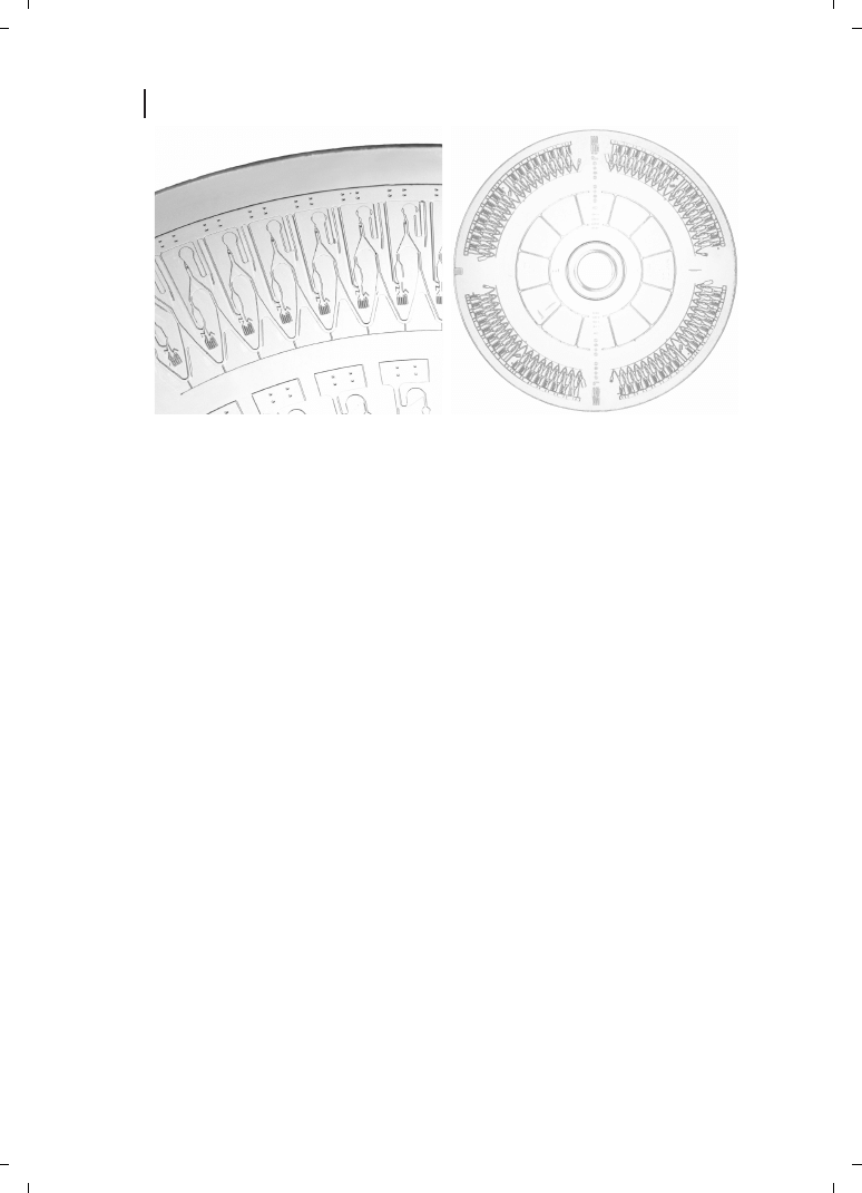
of 96 wells, together with a fluid distribution network, on a single chip is shown in
Figure 2.2.
16
2 Microfluidics Meets Nano : Lab-on-a-Chip Devices and their Potential for Nanobiotechnology
Figure 2.2
Microtiterplate “Lilliput” for bacteria identification and antibiotics susceptibility tests.
Samples are distributed and dosed via a microfluidic network into 96 reaction cavities by capillary forces.
(Courtesy STEAG microParts and Merlin Diagnostika.)

2.2.4
Fluid Transport
Obviously, one important aspect of microfluidic devices is the fluidic transport. One or sev-
eral fluids must be transported to reaction sites, and often a sequence of transport actions at
defined times is required. To achieve the transport, two types of mechanisms are used.
In actively driven transport, active fluidic elements such as pumps and valves are used to
achieve the transport. These may be external elements, but in some cases they are part of
the fluidic device, either by adding them as discrete elements, or by integrating them into
the fluidic device. These active devices require an outside energy supply to operate, and
this can be either electrical, pneumatic, or mechanical. This may require an electrical net-
work to be part of the fluidic system. In one example (the Mixed Circuit Board (MCB) con-
cept, [24]), printed circuit boards have been chosen as the basis for the fluidic device, car-
rying both the fluid microchannels as well as the electrical network. The fluidic elements,
like discrete electrical components, are then assembled on this MCB, which requires both
electrical and fluidic interconnections. In the case of integrated active fluidic elements
(e. g., a piezo-driven membrane pump), it may be of advantage to allow the fluidic struc-
tures such as the pumping chamber, membrane and input and output valves, be part of
the fluidic element. The drive elements like the piezo could then be placed on a separate
drive plate which is attached to the fluidic chip, for example by clamping, during the
operation. In this case, the fluidic chip could be a single-use, disposable device, while
the more expensive drive plate would be re-usable.
Another means of actively providing fluidic transport is the use of mechanical forces. In
the case of centrifugal forces, the fluidic structures are usually on a CD-like substrate,
which is placed on a spinning device which resembles a laboratory centrifuge. The fluidic
transport can be triggered by correct selection of rotational speed, position on the sub-
strate, and channel width. Commercially available platforms include the “LabCD” [25]
and the “Gyrolab
ä microlaboratory” (Figure 2.3).
A major advantage of microfluidics is that fluidic transport can also be achieved in a
passive manner. In this case, capillary forces are used to transport the fluid to the reaction
sites. As mentioned above, capillary forces can be large compared to volume forces in mi-
crofluidics. However, to make use of this effect it is essential that the surface of the fluidic
structures is hydrophilic with respect to the fluids to be transported; this may require a
surface modification of the material (see section 2.3.4).
By correct design of the fluidic structures, the flow front in the device can be controlled,
and this allows the transport times and volumes of the fluids transported to be set to
desired values. For a continuous flow through the device for a long period, larger “waste
reservoirs” are required at the end of the channel network. Locally hydrophobic areas in
the channels may be used to stop the flow at defined positions.
Capillary fluid transport is not reversible, and once the complete fluidic network is
filled, the flow stops. Hence, this transport mechanism is well-suited for priming of the
device, or for single-use, disposable devices. On the other hand, neither an active (and
often expensive) element nor an energy source are needed. This reduces the manufactur-
ing costs and enables the use of microfluidic disposable devices, e. g. in point of care
diagnostics and patient self-testing.
17
2.2 Overview
2.2.5
Stacking and Sealing
Except for some very basic array configurations, all microfluidic devices require a top
cover to create enclosed structures (e. g., channels, reservoirs). This can be achieved by
sealing the top side of the substrate carrying the fluidic structures with a foil, a cover
plate, or by stacking several microstructured fluidic plates.
Sealing with a thin, and often optically transparent foil is a cost-effective procedure and
allows easy access to the fluid, for example when optical methods such as fluorescence are
used as detection methods. Furthermore, special materials may be selected for the foil,
such as foils with high diffusion coefficients for gases, thereby allowing oxygen supply
to cells in the chips.
Cover plates may carry fluidic structures themselves, complementing the fluidic net-
work on the base substrate. One simple example are through-holes in the cover plate
which are used for input and output ports of the fluidic device.
Stacking of several microstructured plates is of advantage for more complex fluidic de-
vices because it is extending integration into the vertical direction. With stacking, multi-
layer fluidic interconnections can be created, and many fluidic devices are much easier to
build when vertical integration is used. One example is that of micropumps, where the
pumping chamber and valve seats may be on one plate, the membrane and the valve
lids on a second, and the driver and input and output on other plates. A very early example
of the stacking principle can be found in the above-mentioned realization of a mTAS
system [18, 26].
If no sealing is used for simple array devices, then hydrophobic surface properties be-
tween the spots may be used to concentrate fluids at the (hydrophilic) spot areas in the
form of droplets, thus avoiding cross-talk between different reaction sites.
18
2 Microfluidics Meets Nano : Lab-on-a-Chip Devices and their Potential for Nanobiotechnology
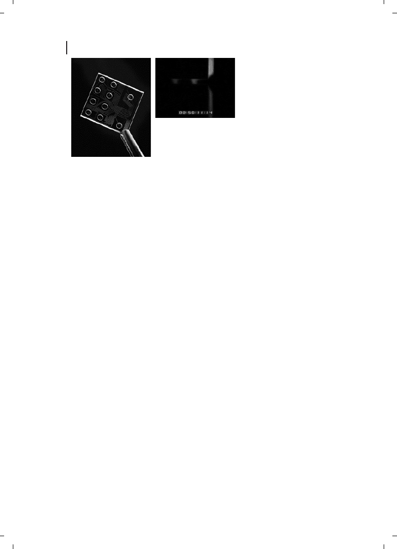
Figure 2.3
Left : Injection-molded CD-like microlaboratory. Right : Close up of the microfluidic structures.
This system enables functions such as volume definition, chromatography, and enzymatic reactions to be
conducted. (Courtesy Gyros AB.)

2.3
Methods
2.3.1
Materials for the Manufacture of Microfluidic Components
Three types of materials are common for microfluidic and Lab-on-a-Chip devices : silicon,
glass, and polymer materials.
2.3.1.1
Silicon
Silicon is the dominant material in microelectronics, and knowledge of micromachining
of this material has been accumulated for several decades. Because of this, silicon has also
been the dominant material used in nonelectronic applications of MEMS and, in the past,
also in microfluidics. In fact, the known micromachining methods for silicon are well-
suited for the generation of high-precision fluidic structures. For example, channels
with square or v-shaped cross-sections can be easily generated.
Among the advantages of silicon are the simple generation of an inert surface (SiO
2
) by
oxidation, high-temperature stability, high chemical resistance to organic solvents and
acids, well-established bonding processes, an extensive knowledge about coatings, and
its well-defined and excellent mechanical properties as a single crystal material.
Silicon may be the material of choice if electric functions such as heaters and sensors
are required as part of the microfluidic component. These can be easily integrated into the
silicon substrate using standard microelectronics fabrication technology.
The disadvantages of silicon are the nonideal surface for many biochemical applica-
tions, and the high price for material and processing. Silicon is a relatively expensive, sin-
gle-crystal material, and the process equipment, process materials from microchip tech-
nology are very expensive. As fluid chips tend to be much larger than electronic chips,
this may lead to high manufacturing costs per chip. Another cost disadvantage is that
the batch processing sequence used for silicon is more complicated than the one-step re-
plication methods used for polymers. In the silicon process, the alignment of subsequent
layers must be carried out for each wafer in production. In polymer replication technology,
the alignment is necessary only during the production of the master, eliminating this
error source once the master has been correctly manufactured.
Furthermore, silicon cannot be used for applications involving electrical fields (e. g.,
capillary electrophoresis) due to its low electrical resistance.
2.3.1.2
Glass
Glass is another important material for the production of microfluidic components and
systems; borosilicate types of glass are often used. Some of these glasses, such as Boro-
float or Pyrex 7740, have thermal expansion coefficients which are matched to that of
silicon, and are used together with silicon in stacked arrangements, for example as trans-
parent cover plates. These glasses can be bonded to silicon by anodic bonding, without the
need of a bonding material.
The advantages of glass are its high chemical resistance, excellent thermal and mechan-
ical stability, and optical transparency. In many cases, glass is well-suited as a surface for
19
2.3 Methods
biological and chemical reactions. There is an extensive knowledge about inorganic and
organic coatings with glass as a base material. Auxiliary electric functions (e. g., heaters)
may be added using the well-established procedures of thin film technology. Glass is also
well-suited for electroosmotic flow applications and capillary electrophoresis [27]. An
example is shown in Figure 2.4.
Although glass as a base material is less expensive than silicon, batch fabrication, opti-
cal polishing steps, and the micropatterning steps will lead to comparatively high produc-
tion costs. Micromachining procedures for glass are much less developed than for silicon,
and in most cases isotropic etching is used. High-aspect ratio and multilevel structures are
difficult to manufacture, and this restricts the use of glass to simple applications such as
array chips, single depth channel networks (e. g., capillary channels), or intermediate and
cover plates in stacked arrangements.
The photostructurable glass FOTURAN (Schott) allows the fabrication of high-aspect
ratio fluidic structures, but the disadvantages are high substrate and processing costs,
and compared to other materials a high surface roughness of the structures.
2.3.1.3
Polymers
Polymers are the third type of material used in the manufacture of microfluidic devices
[28]. The main benefit of polymer materials is based on simple and cost-effective replica-
tion methods such as injection molding or hot embossing, because this allows the man-
ufacture of all microstructures of the device in one manufacturing cycle. The capabilities
of these manufacturing processes in the micro and nano regime are illustrated by the
manufacturing of CDs and DVDs, where a 120 mm-sized device, including metallization
and printing, can be manufactured for much less than 1$ – dramatically less than for a
silicon or glass device of the same size. However, these replication methods require the
manufacture of a master structure, which is used as a tool in the replication step. As
the manufacturing cost of the mastering is considerable, these methods only make
sense for high-volume applications, where at least a few 100 000 parts are manufactured,
and the mastering cost can be shared by many replicated parts.
Another advantage of polymers is the broad range of materials suited for these manu-
facturing methods, including PMMA, PS, PC, cyclic olefins, PEEK, POM, elastomers, and
others. This allows a choice to be made of the material properties suitable for the specific
20
2 Microfluidics Meets Nano : Lab-on-a-Chip Devices and their Potential for Nanobiotechnology
Figure 2.4
Capillary electrophoresis chip for nucleic acid separation.
(Courtesy Caliper Technologies, Inc.)

application. Typical properties of the material that may be of fundamental importance in-
clude optical transparency, autofluorescence, thermal expansion coefficients, and stiffness.
A summary of the properties for a range of materials is provided in Ref. [28].
Convenient sealing methods, such as lamination, ultrasonic welding, laser welding,
gluing or thermal bonding, are available for polymer devices.
One disadvantage of polymer materials is a reduced thermal stability, as these devices
can only be operated at temperatures below the glass transition temperature. This also
limits processes to coat or functionalize the polymer surface. Another disadvantage is
the reduced stability against organic solvents, acids, and bases.
A variety of methods for chemically modifying the plastic surface, and functionalizing
the surface have been published, and extensive work is under way in that field. Most poly-
mer surfaces are not hydrophilic with respect to the fluids used in nanobiotechnology,
and will require a suitable surface modification (e. g., plasma polymerization) if capillary
forces are to be used for fluid transport.
2.3.2
Fluidic Structures
The most basic fluidic structures to build microfluidic devices are microchannels. These
channels provide the fluidic interconnection network between the fluidic elements of the
device, but may have additional functions, like the channels in capillary electrophoresis
and other separation techniques. Various shapes for the channel cross-section are used,
including rectangular, v-shaped, and round. The shape of the cross-section may be deter-
mined by the fabrication method; a review is provided in Ref. [29]. In many cases, the
upper half of the channel contour is flat due to the sealing of the channels by a flat
cover. Interesting exceptions to this are silicon nitride channels with a round cross-section
buried underneath the surface of a silicon substrate [30], or round PDMS channels.
Important parameters of the microchannels include surface roughness and the aspect
ratio of the structure, which is defined as the ratio of depth to width in the case of a chan-
nel. High-aspect ratio channels have a high surface to volume ratio and consume less
floor space on the microfluidic chip. Channel widths commonly vary between the milli-
meter to the micrometer range; aspect ratios up to 10 are used. One microfluidic device
may carry channels of different widths and aspect ratios, for different purposes. For exam-
ple, auxiliary channels are used in capillary devices, with a much smaller diameter than
the fluid channels, to allow the air to exit from the device when it is filled with fluid by
capillary forces.
Other important structures are reaction/detection chambers, and sample and waste
reservoirs. These are larger, well-type structures, with dimensions often in the millimeter
range, designed to hold the correct amount of fluid.
In the case of reaction chambers, it is often advantageous to generate a high surface to
volume ratio. This can be achieved by using auxiliary structures (Figure 2.5), by folding up
a channel in a meander-like form, or by using a porous, nanostructured surface [31].
One special, but important, case of microreaction chambers is that of microcompart-
ments used in array-type microfluidic devices for parallel processing, such as DNA
chips and nanotiter plates. These are designed to hold fluid volumes in the order of
21
2.3 Methods
10 nL to several hundreds of nL. In the most simple case, these compartments will be not
a spatial microstructure at all, but a spot on a flat surface carrying immobilized reagents,
with good wetting properties, and separated from neighboring spots by hydrophobic re-
gions. In the case of nanotiterplates, the bottom of the compartments may be a thin mem-
brane, so that optical detection techniques can be applied through the membrane from
the bottom side. For applications in combinatorial chemistry, where the possibility to
wash and filter reagents is essential, these membranes may be patterned to contain
pores in the nanometer or micrometer range.
Active and passive valves are needed to block the fluid flow in a controlled manner.
Valves may be used as discrete devices, or integrated into the fluidic chip. Technically, can-
tilever and diaphragm-type valves are used; reviews are provided in Refs. [32, 33]. Fluidic
diodes, which do not have any moving parts [34], are also used; these do not block the flow
in one direction completely, but provide a large difference in impedance. Moreover, they
are easy to integrate into the system.
Propagation of fluids in the chip is achieved by the use of micropumps which, as in the
case of valves, may be either external or integrated into the microfluidic device. Techni-
cally, most micropumps are membrane-actuated pumps, using pneumatic, thermopneu-
matic, piezoelectric, electrostatic, bimetallic, or shape-memory effects for actuation.
Some electric field-actuated pumps (electrohydrodynamic and electroosmotic) and
micro gear pumps are also available; an overview is provided in Refs. [32, 33].
As flow in microfluidic devices is strictly laminar, mixing must be initiated using a spe-
cially designed element, a micromixer. Most micromixers are static mixers, which are ex-
clusively based on the diffusion of the liquids to be mixed. Diffusion requires time, and
this must be provided in the microsystem by using long, parallel flow regions and having
large interfaces between the liquids to be mixed. This is often achieved by multiple split-
ting of the fluid strand, and recombining. Methods to go beyond laminar mixing include
22
2 Microfluidics Meets Nano : Lab-on-a-Chip Devices and their Potential for Nanobiotechnology
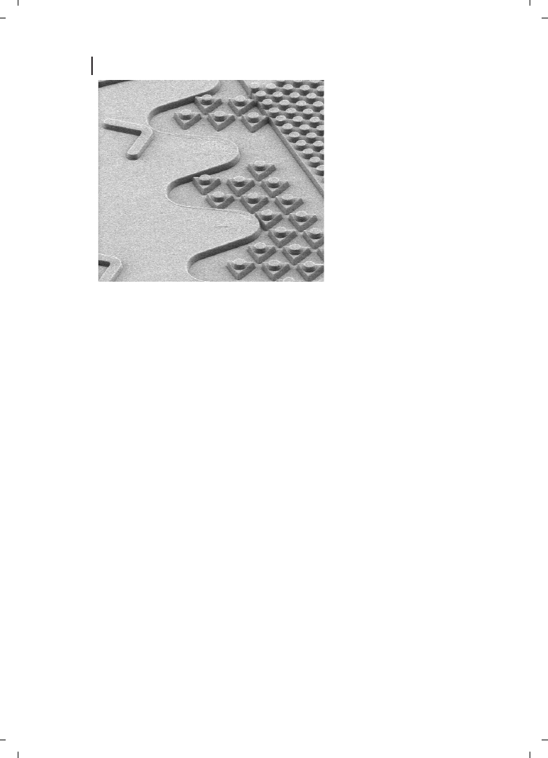
Figure 2.5
Scanning electron micro-
graph of auxiliary structures in a mi-
crofluidic chamber. These are designed
to generate a large surface to volume
ratio. (Courtesy STEAG microParts.)

the use of microbeads [35] and chaotic mixing using relief structures at the channel bot-
tom [36]. A review of mixers is provided in Ref. [33].
Other fluidic structures in microfluidic devices include sensors for physical parameters
such as pressure, temperature, and flow, as well as chemical sensors and biosensors. Such
elements are found in Lab-on-a-Chip devices, while in single-use disposable fluidic
devices these more expensive systems will not be part of the fluidic device.
2.3.3
Fabrication Methods
The fluidic structures are fabricated using standard methods of microfabrication. These
are well-documented in standard textbooks of microsystem technology, for example by
Menz and Mohr [37] or Madou [38], and are beyond the scope of this chapter. Other sum-
maries of fabrication technology, more specific for the application to fluid devices, may be
found in Refs. [32, 39].
These microfabrication methods are also used to manufacture the master tool for the
microreplication of polymers. The master is usually a metal (or in some cases a silicon)
tool. The master structure is the inverse of the fluidic structure to be generated in the
replication process. Channels, for example, will be a line on the master.
Practical, marketable fluidic devices are generally multilevel structures. This means
that a device will not carry structures of one common structural depth only, but will
have channels, wells, and reservoirs with a variety of structural depths. This cannot
usually be achieved with one single fabrication step, nor by using just one fabrication
technology, and in practice a combination of different fabrication technologies, each
suitable for the generation of structures of the desired size, shape, and precision, will
have to be applied. For example, in the fabrication sequence of a replication master, the
channel structures for small channel diameters could be fabricated by lithography
and electroplating, the more coarse channels by milling, and through holes by spark
erosion.
2.3.4
Surface Modifications
Modifications of the surface of the device are essential for the designed functionality of
microfluidic devices in (nano)biotechnology. Often, these modifications are to be achieved
locally, and therefore different areas of the device will require different modifications.
These modifications must be achieved on all surfaces, including the sidewalls of high-
aspect ratio microstructures, for example in deep channels.
The objectives for modifications of the fluidic device surface include the modification of
wetting characteristics (hydrophobic/hydrophilic), increased biocompatibility, reducing or
eliminating solute interactions with the device surfaces, modifying electroosmotic flow,
immobilizing the reagents, enzymes, antibodies, proteins, DNA, etc. to carry out chemical
reactions or detection mechanisms, or to provide a proper surface for immobilization, in-
creasing the surface area for catalytic reactions, and tethering sieving matrices or station-
ary phases for separation devices.
23
2.3 Methods

The surface modifications may be achieved by a variety of techniques, including CVD
and PVD methods, spin coating and solution casting, plasma processes (e. g., plasma etch-
ing and plasma polymerization), grafting, chemical self-assembly, the Langmuir–Blodgett
technique, printing, and others. In some cases, these surface modifications will involve
nanotechnology. The thickness of the modification layer is in the nanometer range;
thicker layers might modify the device geometry, and its function, and so for the objective
of the functionalization, often only a few monolayers are sufficient.
For example, when multilayer films containing ordered layers of protein species are
assembled by means of alternate electrostatic absorption with positively charged PEI,
PAH, chitosan or with negatively charged PSS, DNA and heparin, the enzymatic activity
of the films does not increase with layer number for more than 10–15 layers [40].
Requirements which the surface modifications must meet include good adhesion,
chemical stability against the media used in the device, and a time stability which is better
than the lifetime of the device.
One very important surface modification is that of modifying the wetting characteristics
of the surface. As the interfacial tensions cannot be monitored directly, measurement of
the contact angle between the surface and a droplet of liquid is widely used to characterize
the wetting characteristics of the surface.
Materials such as glass, Si and SiO
2
have many OH-groups on their surfaces, and this
causes hydrophilic behavior. Especially in the case of silicon, the wettability depends
strongly on the pre-treatment and history of the surface. Hydrophobic surfaces may be
produced using octadecyltrichlorosilane (OCTS), and hydrophilic behavior may be stabi-
lized using hexamethydisilazane (HMDS).
Polymer surfaces are hydrophobic in most cases. Hydrophilic surfaces may be easily
generated using O
2
plasma treatment, but such surfaces are stable only for a few days.
More stable surface modifications are obtained by plasma polymerization of layers invol-
ving OH-groups at the surface.
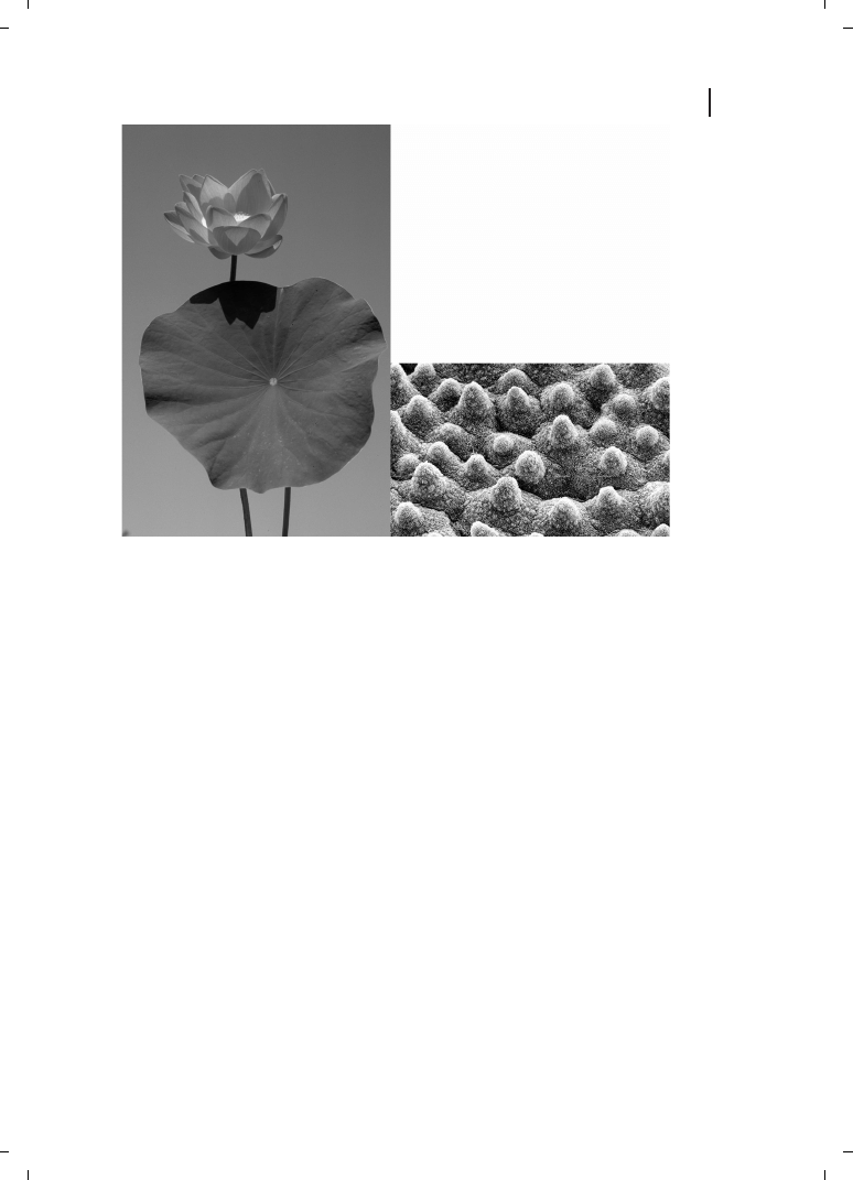
The wetting characteristics of the surface may also be modified by a nanostructured sur-
face. This principle of nanobiotechnology is found in nature, for example, in the cuticular
structure of leaf surfaces [41] and in fractal surfaces [42]. Such water-repelling surfaces
have self-cleaning properties (the Lotus effect), as particles on nanostructured hydropho-
bic surfaces are more readily wetted and washed away (Figure 2.6).
Large surface areas are required for both catalytic reactions and separation assays, and
this may be achieved by coating microfluidic chips with a porous material. In the case of
silicon, porous silicon with pore sizes in the nanometer to micrometer range may be
generated.
Another important surface functionalization is the binding of specific molecules
to designated areas of the chip. Such applications include DNA-, proteomics-, cell-, and
tissue-chips. Generally, by using various surface chemistries, linkers for such mole-
cules must be provided in designated areas, while the remaining surface should be non-
binding.
Methods to immobilize the specific molecules include adsorption, crosslinking, covalent
binding, microencapsulation, and entrapment. A thin, sputtered gold film can be used to
immobilize a dense molecular film of thiols [43], providing a high density of alkyl groups
as binding sites for surface reactions.
24
2 Microfluidics Meets Nano : Lab-on-a-Chip Devices and their Potential for Nanobiotechnology
One example of polymer substrates is the building of a functional chemical scaffold on
PMMA using an ethylene diamine foundation [44]. In this way, various materials such as
oligonucleotides, enzymes, or stationary phases may be attached to the device surface.
2.3.5
Spotting
For array-type microfluidic devices, large numbers of molecules must be collected and
placed either in defined microvessels, as with libraries in solution in nanotiter plates,
or at defined spots on the surface of a carrier for probe molecules being immobilized
on the substrate. This requires the microdispensing of a large variety of (different) fluids
in drop volumes down to the picoliter range, with spot sizes and drop distances down to
some 10 mm. Special devices to accomplish this task – the “spotters” – have been devel-
oped, and a review of spotting methods is provided in Ref. [45].
Dedicated capture spots with optimized wetting characteristics for the dispensed liquid,
and non-wetting bars between these spots, may support the array production using spot-
ters.
The main types of spotting methods currently in use include pin-based spotting, ink-jet
spotting, photolithographic synthesis, electronic addressing, and stamping.
In pin-based spotting, an array of metal (tungsten) pins picks up a small volume
each by dipping into a well plate, and then transfers it when touched down onto the sub-
strate.
25
2.3 Methods
Figure 2.6
Left :
Nelumbo nucifera, the Lotus flower.
Right : a double-structured surface optimized for self-
cleaning. Contact areas are minimized through the
combination of micro- (cells) and nanostructures (wax
crystals). (Courtesy University of Bonn.)

Ink-jet spotting uses proven technology from piezoelectric printheads of ink-jet print
technology. Large arrays of heads are used for spotting with good control of drop sizes
down to the pL range, at high speed.
Photolithographic synthesis is a method developed by Affymetrix [46], where capture
probes are synthesized directly on the chip. Photolithography masks the direct, light-sen-
sitive removal of protective groups from hydroxyls in the exposed regions. This allows spe-
cific protected nucleotides to attach to these hydroxyls, after which the process is repeated
for the next nucleotide.
In the electronic addressing method developed by Nanogen [47], use is made of the fact
that the biologic target material is usually either positively or negatively charged. By set-
ting voltage potentials at the test sites of the array, the target can be attracted and docked
at these sites. However, this method requires full semiconductor processing in the man-
ufacture of the array.
Another spotting method currently under development is that of micro contact printing
(see Chapter 3). Elastomeric stamps with posts in the mm size region are used to deliver
either the reagent of choice, or a deprotecting agent, to the spots.
2.3.6
Detection Mechanisms
For most microfluidic applications, detection devices are not integrated into the fluidic
chip, but form part of a separate (in many cases highly automated) handling and detection
system. In this way, the system can be re-used for the evaluation of a large number of
chips.
One problem associated with detection in microfluidic devices is the small sample
volume. For example, due to the small dimensions of the system, the optical pathlength
for absorption measurements is also likely to be very small.
Commonly used detection methods include absorption (ultra-violet, optical, infra-red),
fluorescence, luminescence, electrochemical, thermal or electrical conductivity, and
others. Several miniaturized or even microstructured detection systems are available,
one example being that of micromolded microspectrophotometers [48].
2.4
Outlook
During the past few years, microsystem technologies – and especially microfluidics for
Life Sciences applications – have been identified as the enabling technology of the 21st
century. A variety of biomicrosystems has been developed, and research and commercia-
lization efforts on bioMEMS, biochips and Lab-on-a-Chip devices are booming. Today, less
than two decades after MEMS technology first emerged, nanotechnology – again, often
focused on biology – has begun to attract the interest of the research community. Cur-
rently, it is considered that nanobiotechnology will have at least the same impact as
bioMEMS technology has had in the past.
On one hand, due to a top-down approach and a continuous shift of technical limits
(e. g., resolution), an extension from microstructures to nanostructures has been antici-
26
2 Microfluidics Meets Nano : Lab-on-a-Chip Devices and their Potential for Nanobiotechnology

pated. Nanofluidics, nanooptics, nanomechanics, and nanoelectronics will be disciplines
that derive naturally from their larger counterparts, not predecessors. When favorable
for the envisioned assay, nanochannels, nanocavities, nanoposts and other structural fea-
tures will be used instead of (or in combination with) microstructures [49], and nanoelec-
trodes or nanooptical structures will enable further progress in detection technologies and
sensitivity.
On the other hand, due to a bottom-up approach, nanosystems will need microfluidic
devices as a physical interface to instruments or humans. A variety of examples for the
bottom-up approach, often in combination with novel, nanoanalytical characterization
methods, are described in detail in other chapters of this book. Most functionality will
be created when bottom-up and top-down strategies are combined, whereupon microflui-
dics and nanobiotechnology will emerge towards integrated systems. Nanostructures such
as self-assembled systems or biomimetic surfaces, nanocoatings, nanopores, nanoactua-
tors, nanoparticles, nanocomposites, nanobarcodes or nanoelectrodes will enable novel
microfluidic devices for Life Science applications such as drug discovery, diagnostics,
and therapy.
Nanoparticles and nanocoatings have been already established for microfluidic devices.
Commercially available lateral flow immunoassays involve biofunctionalized particles in
the nano range, and magnetic nanoparticles are used for the purification of biomolecules
such as cells or nucleic acids. Nanobarcodes – sub-mm-sized metal particles functionalized
with biomolecules, comprise freestanding, cylindrically shaped metal nanoparticles that
are self-encoded with sub-mm stripes. Intrinsic differences in reflectivity between adjacent
metal stripes (e. g., gold and silver) of the nanobarcodes allow individual particles to be
identified by conventional optical microscopy. Nanobarcode particles are thus the nanos-
cale equivalent of conventional bar codes, and are used to decode the sample bound to the
functionalized particle surface; for details, see Chapter 26.
Nanocoatings are derived from “conventional” surface chemistry, and also have been
found in nature. One of the most impressive examples of biomimicry has been the
Lotus effect. This phenomenon of superhydrophobic, self-cleaning surfaces which is
seen not only in the Lotus flower but also in many other leaves (e. g., cabbage, reeds, In-
dian cress, tulips) as well as in animals (e. g., wings of butterflies and dragonflies), has
been explored in detail by W. Barthlott and others [41]. The self-cleaning property is con-
nected with a microstructured surface as well as with a coating of water-repellent waxy
crystals. Besides inorganic contamination, organic contaminations such as spores, bac-
teria or algae play an important role in plants. An elegant way to cope with this is to
use the Lotus effect, which prevents pathogens from binding to the leaf surface. As the
Lotus effect is based solely on physico-chemical properties and is not bound to a living
system, artificial self-cleaning surfaces have been successfully manufactured, and such de-
vices for Life Science applications are currently being tested. Nanocoatings with other
functionalities are also under development; for example, for guided migration, spreading,
growth and differentiation of cells in culture, for the enhanced integrity of biological
samples, or for a controlled release of embedded drugs.
Both nanocoatings and nanostructures are currently being evaluated for tissue engineer-
ing [50]. Another approach to mimic nature is that of molecular imprinting technology
(MIT), which can be described as making artificial ‘locks’ for ‘molecular keys’. Although
27
2.4 Outlook

molecular imprinting was used as early as the 1930s by Polyakov to selectively capture var-
ious additives in a silica matrix, progress has been comparably slow. Recently, a team of
chemists at the University of Illinois developed a way of creating artificial antibodies by
using a process in which a single molecular template is imprinted into a single macromo-
lecule – a highly branched polymer called a dendrimer. Upon removal of the template, a
synthetic molecular shell is created, which can bind specifically shaped molecules and
can, like a natural antibody, reject others [51].
In principle, the molecular key may be any type of molecule, ranging from small mo-
lecules (e. g., drugs, amino acids, steroid hormones) to larger molecules (e. g., nucleic
acids, proteins). Large molecular assemblies such as cells and viruses may also be per-
ceived, though the difficulty of making the imprinted materials increases with the size
of the selected key molecule. A combination of MIT and future Lab-on-a-Chip devices pro-
mises many advantages for Life Science applications, although in this case the period
between proof-of-principle and commercialization is likely to be long.
The use of nanopores in Life Science applications leads to another interesting field of
research. Current investigations on nanopore membranes include patch–clamp arrays,
biocapsules for biosensor protection, and drug delivery systems, for example nanopore
membranes as functional parts of subcutaneous implants or microparticles with
nanopores, such as porous silicon particles. Nanopores are also currently under investiga-
tion for use in haplotyping, SNP detection, and DNA sequencing [52, 53]. A detailed over-
view is provided in Chapter 7.
An additional impact on microfluidic devices is expected from nanomechanics. One
such embodiment is that of silicon cantilevers in a Lab-on-a-Chip; these are a few hundred
nanometers thick, and have biomolecules (e. g., antibodies) attached to one side. The bind-
ing of protein molecules to the capture antibodies causes the cantilevers to bend, and this
can be monitored either electronically or optically [20]. Another class of actuators which,
as in muscles, harnesses molecular deformations to generate meso- and macroscopic
forces and displacement, are the conductive or electroactive polymers (EAPs) [54, 55].
These materials, which undergo large conformational changes in response to electrical
or chemical stimuli, might be well suited for actuators, regulators, valves or sensors of
future bioMEMS, respectively bioNEMS generations.
28
2 Microfluidics Meets Nano : Lab-on-a-Chip Devices and their Potential for Nanobiotechnology

29
References
References
[1]
S. C. Terry, J. H. Hermann, J. B. Angell,
IEEE Trans. Elec. Dev. 1979, 26, 1880.
[2]
A. Manz, N. Graber, Sensors and Actuators
1990, B1, 244.
[3]
Detailed information about microreaction
technology may be found in the proceed-
ings on the annual International Con-
ference on Microreaction Technology,
W. Ehrfeld (ed.), Microreaction Technology:
Industrial Prospects, Springer, Berlin 2000.
[4]
E. Bassous, H. H. Taub, L. Kuhn, Appl.
Phys. Lett. 1977, 31, 135.
[5]
A. Emmer, M. Jansson, J. Roeraade,
U. Lindberg, J. Microcolumn Separation
1992, 4, 13.
[6]
R. Zengerle, A. Richter, H. Sandmaier,
Proc IEEE Micro Electro Mechanical
Systems, Travemünde, Germany, 1992,
19.
[7]
F. C. M. van der Pol, H. T. G. van Lintel,
M. Elwenspoek, J. H. J. Fluitman, Sensors
and Actuators 1990, A21, 198.
[8]
S. T. Cho, K. D. Wise, Proc Transducers
1991, Sans Francisco, USA, 1991, 400.
[9]
M. de la Guardia, Microchim. Acta 1995,
120, 243.
[10]
S. Shoji, S. Nakagawa, M. Esashi, Sensors
and Actuators 1990, A21, 189.
[11]
M. Richter, A. Prak, J. Naundorf, M. Eberl,
H. Leewis, W. Woias, A. Steckenborn, Proc
Transducers 1997, Chicago, USA, 1997,
303.
[12]
B. H. van der Schoot, S. Jeanneret, A. van
den Berg, N. F. de Rooij, Sensors and
Actuators 1993, B15, 211.
[13]
G. Mayer, K. Wohlfahrt, A. Schober, J. M.
Köhler, Nanotiterplates for screening and
synthesis, in : J. M. Köhler, T. Mejevaia,
H. P. Saluz (eds), Microsystem Technology:
A Powerful Tool for Biomolecular Studies,
Birkhäuser-Verlag, Basel, 1999, 75.
[14]
V. Grosser, H. Reichl, H. Kergel, M. Schü-
nemann, A Fabrication Framework for
Modular Microsystems, MST News 2000,
1, 4.
[15]
H. M. Widmer, Analytical Methods and
Instrumentation, Special Issue mTAS ’96,
1996, 3.
[16]
A. van den Berg, P. Bergveld, Analytical
Methods and Instrumentation, Special Issue
m
TAS ’96, 1996, 9.
[17]
Y. Baba et al. (eds), Micro Total Analysis
Systems 2002, Kluwer Academic Publishers,
2002.
[18]
H. Lüdi, M. B. Garn, S. D. Hämmerli,
A. Manz, H. M. Widmer, J. Biotechnol.
1992, 25, 75.
[19]
M. U. Kopp, A. J. de Mello, A. Manz,
Science 1998, 280, 1046.
[20]
J. Liu, M. Enzensberger, S. Quake, Electro-
phoresis 2002, 23, 1531.
[21]
M. T. Taylor, P. Belgrader, R. Joshi, G. A.
Kintz, M. A. Northrup, Micro Total Analysis
Systems 2001, 670.
[22]
A. Manz, D. J. Harrison, E. Verpoorte, J. C.
Fettiger, A. Paulus, H. Lüdi, H. M. Widmer,
J. Chromatogr. 1992, 593, 1926.
[23]
M. Koch, A. Evans, A. Brunnschweiler,
Microfluidic Technology and Applications,
Research Studies Press, Philadelphia,
2000.
[24]
T. S. J. Lammerink, V. L. Spiering, M. El-
wenspoek, J. H. J. Fluitman, A. van den
Berg, Proc MEMS 1996, San Diego, USA,
1996, 389.
[25]
D. C. Duffy, H. L. Gillis, J. Lin, N. F. Shep-
pard, Jr., G. J. Kellog, Anal. Chem. 1999, 71,
20, 4669.
[26]
M. Busch, J. Schmidt, A. Rothen, C. Leist,
B. Sonnleitner, E. Verpoorte, Proc 2nd Int
Symp mTAS, Basel, 1996.
[27]
G. J. M. Bruin, Electrophoresis 2000, 21,
3931.
[28]
H. Becker, L. E. Locascio, Talanta 2002,
56, 267.
[29]
J. G. E. Gardeniers, R. W. Tjerkstra, A. van
den Berg, Fabrication and Application of
Silicon-based Microchannels, in : W. Ehr-
feld (ed.), Microreaction Technology: Indus-
trial Prospects, Springer, Berlin, 2000, 36.
[30]
R. W. Tjerkstra, M. J. deBoer, J. B. Beren-
schot, J. G. E. Gardeniers, M. C. Elwen-
spoek, A. van den Berg, Proc IEEE Work-
shop on MEMS, Nagoya, Japan, 1997, 147.
[31]
J. Drott, K. Lindstrom, L. Rosengren, T. L.
Aurell, J. Micromech. Microeng. 1997, 7, 14.

30
2 Microfluidics Meets Nano : Lab-on-a-Chip Devices and their Potential for Nanobiotechnology
[32]
M. Koch, A. Evans, A. Brunnschweiler,
Microfluidic Technology and Applications,
Research Studies Press, 2000, Chapter 6.3.
[33]
S. Howitz, Components and systems for
microliquid handling, in : J. M. Köhler,
T. Mejevaia, H. P. Saluz (eds), Microsystem
Technology: A Powerful Tool for Biomolecular
Studies, Birkhäuser Verlag, Basel, 1999, 31.
[34]
T. Gerlach, H. Wurmus, K. Helmut,
Working principle and performance of the
dynamic micropump, Sensors and Actuators
1995, 50, 135–140.
[35]
G. H. Seong, R. M. Crooks, J. Am. Chem.
Soc. 2002, 124, 13360.
[36]
A. D. Stroock, S. K. W. Dertinger, A. Ajdari,
I. Mezic, H. A. Stone, G. M. Whitesides,
Science 2002, 295, 647.
[37]
W. Menz, J. Mohr, O. Paul, Microsystem
Technology, Wiley-VCH, Weinheim, 2001.
[38]
M. J. Madou, Fundamentals of Microfabrica-
tion : The Science of Miniaturization, CRC
Press, Boca Raton, 2002.
[39]
M. Gad-el-Hak (ed.), The MEMS Handbook,
CRC Press, Boca Raton, Chapter 16, 2002.
[40]
M. Onda, K. Ariga, T. Kunitake, J. Ferment.
Bioeng. 1999, 87, 87.
[41]
C. Neinhuis, W. Barthlott, Ann. Bot. 1979,
79, 667.
[42]
S. Shibuichi, T. Onda, N. Satoh, K. Tsuij,
J. Phys. Chem. 1996, 100, 19512.
[43]
M. Mrksich, G. M. Whitesides, Trends
Biotechnol. 1995, 13, 228.
[44]
S. Soper, in : J. Göttert (ed.), 2001 CAMD
Summer School Micro-and Nanotechnologies,
Chapter 10, Baton Rouge, CAMD/LSU
Publishers, 2001.
[45]
M. Pirrung, Angew Chem Int Ed, 2002, 41,
1276.
[46]
M. J. Heller, DNA Microarray Technology:
Devices, Systems and Applications, Annu.
Rev. Biomed. Eng. 2002, 4, 159.
[47]
R. Sosnowski, M. J. Heller, E. Tu, A. H.
Forster, R. Radtkey, Active microelectronic
array system for DNA hybridisation, geno-
typing and pharmacogenomic applications,
Psychiatr. Genet. 2002, 12, 181.
[48]
D. Brennan, Infrared Physics Technol. 2002,
43, 69–76.
[49]
S. R. Quake, A. Scherer, From Micro to
Nano Fabrication with Soft Materials,
Science 2000, 290, 1536.
[50]
S. Bhatia, Microfabrication in Tissue Engi-
neering and Bioartificial Organs, Kluwer,
Boston, 1999.
[51]
S. C. Zimmerman, M. S. Wendland, N. A.
Rakow, I. Zharov, K. S. Suslick, Synthetic
Hosts by Monomolecular Imprinting
Inside Dendrimers, Nature 2002, 418,
399–403.
[52]
A. Marziali, M. A. Akeson, New DNA
Sequencing Methods, Annu. Rev. Biomed.
Eng. 2001, 3, 195–223.
[53]
D. W. Deamer, D. Branton, Characterisa-
tion of nucleic acids by nanopore analysis,
Chem. Res. 2002, 35, 817–825.
[54]
Y. Bar-Cohen (ed.), Electroactive Polymer
Actuators as Artificial Muscles, SPIE Press,
Bellingham, 2001.
[55]
J. D. Madden, P. G. Madden, I. W. Hunter,
Conductive Polymer Actuators as Engi-
neering Materials, SPIE 9th Annual Sym-
posium on electroactive materials and
structures, San Diego, CA, USA, Vol. 4695,
pp. 424–434, March 18–21, 2002.
Wyszukiwarka
Podobne podstrony:
Wyk 02 Pneumatyczne elementy
02 OperowanieDanymiid 3913 ppt
02 Boża radość Ne MSZA ŚWIĘTAid 3583 ppt
OC 02
PD W1 Wprowadzenie do PD(2010 10 02) 1 1
02 Pojęcie i podziały prawaid 3482 ppt
WYKŁAD 02 SterowCyfrowe
02 filtracja
02 poniedziałek
21 02 2014 Wykład 1 Sala
Genetyka 2[1] 02
02 czujniki, systematyka, zastosowania
auksologia 13 02 2010
02 MAKROEKONOMIA(2)id 3669 ppt
więcej podobnych podstron