
1
PCB Design Guidelines
For Reduced EMI
SZZA009
November 1999

2
IMPORTANT NOTICE
Texas Instruments and its subsidiaries (TI) reserve the right to make changes to their products
or to discontinue any product or service without notice, and advise customers to obtain the latest
version of relevant information to verify, before placing orders, that information being relied on
is current and complete. All products are sold subject to the terms and conditions of sale supplied
at the time of order acknowledgement, including those pertaining to warranty, patent
infringement, and limitation of liability.
TI warrants performance of its semiconductor products to the specifications applicable at the
time of sale in accordance with TI’s standard warranty. Testing and other quality control
techniques are utilized to the extent TI deems necessary to support this warranty. Specific testing
of all parameters of each device is not necessarily performed, except those mandated by
government requirements.
CERTAIN APPLICATIONS USING SEMICONDUCTOR PRODUCTS MAY INVOLVE
POTENTIAL RISKS OF DEATH, PERSONAL INJURY, OR SEVERE PROPERTY OR
ENVIRONMENTAL DAMAGE (“CRITICAL APPLICATIONS”). TI SEMICONDUCTOR
PRODUCTS ARE NOT DESIGNED, AUTHORIZED, OR WARRANTED TO BE SUITABLE FOR
USE IN LIFE-SUPPORT DEVICES OR SYSTEMS OR OTHER CRITICAL APPLICATIONS.
INCLUSION OF TI PRODUCTS IN SUCH APPLICATIONS IS UNDERSTOOD TO BE FULLY
AT THE CUSTOMER’S RISK.
In order to minimize risks associated with the customer’s applications, adequate design and
operating safeguards must be provided by the customer to minimize inherent or procedural
hazards.
TI assumes no liability for applications assistance or customer product design. TI does not
warrant or represent that any license, either express or implied, is granted under any patent right,
copyright, mask work right, or other intellectual property right of TI covering or relating to any
combination, machine, or process in which such semiconductor products or services might be
or are used. TI’s publication of information regarding any third party’s products or services does
not constitute TI’s approval, warranty or endorsement thereof.
Copyright
1999, Texas Instruments Incorporated

iii
Contents
Title
Page
ABSTRACT
1
. . . . . . . . . . . . . . . . . . . . . . . . . . . . . . . . . . . . . . . . . . . . . . . . . . . . . . . . . . . . . . . . . . . . . . . . . . . . . . . . . . . . . . .
1 Background
1
. . . . . . . . . . . . . . . . . . . . . . . . . . . . . . . . . . . . . . . . . . . . . . . . . . . . . . . . . . . . . . . . . . . . . . . . . . . . . . . . . . . . .
1.1 RF Sources
1
. . . . . . . . . . . . . . . . . . . . . . . . . . . . . . . . . . . . . . . . . . . . . . . . . . . . . . . . . . . . . . . . . . . . . . . . . . . . . . . .
1.2 Surface-Mount Devices vs Through-Hole Components
1
. . . . . . . . . . . . . . . . . . . . . . . . . . . . . . . . . . . . . . . . . . . . . .
1.3 Static Pins vs Active Pins vs Inputs
1
. . . . . . . . . . . . . . . . . . . . . . . . . . . . . . . . . . . . . . . . . . . . . . . . . . . . . . . . . . . . .
1.4 Basic Loops
2
. . . . . . . . . . . . . . . . . . . . . . . . . . . . . . . . . . . . . . . . . . . . . . . . . . . . . . . . . . . . . . . . . . . . . . . . . . . . . . . .
1.4.1 Proportionality of Loops and Dipoles
3
. . . . . . . . . . . . . . . . . . . . . . . . . . . . . . . . . . . . . . . . . . . . . . . . . . . . .
1.5 Differential vs Common Mode
3
. . . . . . . . . . . . . . . . . . . . . . . . . . . . . . . . . . . . . . . . . . . . . . . . . . . . . . . . . . . . . . . . .
2 Board Layout
4
. . . . . . . . . . . . . . . . . . . . . . . . . . . . . . . . . . . . . . . . . . . . . . . . . . . . . . . . . . . . . . . . . . . . . . . . . . . . . . . . . . . .
2.1 Grounds and Power
4
. . . . . . . . . . . . . . . . . . . . . . . . . . . . . . . . . . . . . . . . . . . . . . . . . . . . . . . . . . . . . . . . . . . . . . . . . .
2.1.1 Inductance
4
. . . . . . . . . . . . . . . . . . . . . . . . . . . . . . . . . . . . . . . . . . . . . . . . . . . . . . . . . . . . . . . . . . . . . . . . . . .
2.1.2 Two-Layer vs Four-Layer Boards
4
. . . . . . . . . . . . . . . . . . . . . . . . . . . . . . . . . . . . . . . . . . . . . . . . . . . . . . . . .
2.1.3 Microcomputer Grounds in One- and Two-Layer Designs
5
. . . . . . . . . . . . . . . . . . . . . . . . . . . . . . . . . . . . .
2.1.4 Signal Return Grounds
5
. . . . . . . . . . . . . . . . . . . . . . . . . . . . . . . . . . . . . . . . . . . . . . . . . . . . . . . . . . . . . . . . .
2.1.5 Analog vs Digital vs High Power
5
. . . . . . . . . . . . . . . . . . . . . . . . . . . . . . . . . . . . . . . . . . . . . . . . . . . . . . . . .
2.1.6 Analog Power-Supply Pins and Analog Reference Voltages
6
. . . . . . . . . . . . . . . . . . . . . . . . . . . . . . . . . . . .
2.1.7 Power Plane Do’s and Dont’s for Four-Layer Boards
6
. . . . . . . . . . . . . . . . . . . . . . . . . . . . . . . . . . . . . . . . .
2.2 Power Distribution for Two-Layer Boards
7
. . . . . . . . . . . . . . . . . . . . . . . . . . . . . . . . . . . . . . . . . . . . . . . . . . .
2.2.1 Single-Point vs Multipoint Distribution
7
. . . . . . . . . . . . . . . . . . . . . . . . . . . . . . . . . . . . . . . . . . . . . . . . . . . .
2.2.2 Star Distribution
7
. . . . . . . . . . . . . . . . . . . . . . . . . . . . . . . . . . . . . . . . . . . . . . . . . . . . . . . . . . . . . . . . . . . . . .
2.2.3 Gridding to Create Planes
7
. . . . . . . . . . . . . . . . . . . . . . . . . . . . . . . . . . . . . . . . . . . . . . . . . . . . . . . . . . . . . . .
2.2.4 Bypassing and Ferrite Beads
9
. . . . . . . . . . . . . . . . . . . . . . . . . . . . . . . . . . . . . . . . . . . . . . . . . . . . . . . . . . . .
2.2.5 Keeping Noise Close to the Chip
11
. . . . . . . . . . . . . . . . . . . . . . . . . . . . . . . . . . . . . . . . . . . . . . . . . . . . . . . .
2.3 Board Zoning
12
. . . . . . . . . . . . . . . . . . . . . . . . . . . . . . . . . . . . . . . . . . . . . . . . . . . . . . . . . . . . . . . . . . . . . . . . .
2.4 Signal Traces
13
. . . . . . . . . . . . . . . . . . . . . . . . . . . . . . . . . . . . . . . . . . . . . . . . . . . . . . . . . . . . . . . . . . . . . . . . . . . . . .
2.4.1 Capacitive and Inductive Crosstalk
13
. . . . . . . . . . . . . . . . . . . . . . . . . . . . . . . . . . . . . . . . . . . . . . . . . . . . . .
2.4.2 Antenna Factor Length Rules
13
. . . . . . . . . . . . . . . . . . . . . . . . . . . . . . . . . . . . . . . . . . . . . . . . . . . . . . . . . . .
2.4.3 Series Termination, Transmission Lines
13
. . . . . . . . . . . . . . . . . . . . . . . . . . . . . . . . . . . . . . . . . . . . . . . . . . .
2.4.4 Impedance Matching at Inputs
14
. . . . . . . . . . . . . . . . . . . . . . . . . . . . . . . . . . . . . . . . . . . . . . . . . . . . . . . . . .
2.5 Cables and Connectors
14
. . . . . . . . . . . . . . . . . . . . . . . . . . . . . . . . . . . . . . . . . . . . . . . . . . . . . . . . . . . . . . . . . . . . . .
2.5.1 Differential-Mode and Common-Mode Noise
14
. . . . . . . . . . . . . . . . . . . . . . . . . . . . . . . . . . . . . . . . . . . . . .
2.5.2 Crosstalk Model
14
. . . . . . . . . . . . . . . . . . . . . . . . . . . . . . . . . . . . . . . . . . . . . . . . . . . . . . . . . . . . . . . . . . . . .
2.5.3 Number of Returns
15
. . . . . . . . . . . . . . . . . . . . . . . . . . . . . . . . . . . . . . . . . . . . . . . . . . . . . . . . . . . . . . . . . . .
2.5.4 I/O Recommendations for Off-PCB Signals
15
. . . . . . . . . . . . . . . . . . . . . . . . . . . . . . . . . . . . . . . . . . . . . . .
2.5.5 Keeping Noise and Electrostatic Discharge (ESD) Out
15
. . . . . . . . . . . . . . . . . . . . . . . . . . . . . . . . . . . . . . .
2.6 Other Layout Issues
15
. . . . . . . . . . . . . . . . . . . . . . . . . . . . . . . . . . . . . . . . . . . . . . . . . . . . . . . . . . . . . . . . . . . . . . . . .
2.6.1 Front-Panel PCB with Keypad and Display in Automotive and Consumer Applications
15
. . . . . . . . . . . . .
2.6.2 Layout for Susceptibility
16
. . . . . . . . . . . . . . . . . . . . . . . . . . . . . . . . . . . . . . . . . . . . . . . . . . . . . . . . . . . . . .
2.6.3 Autorouters
16
. . . . . . . . . . . . . . . . . . . . . . . . . . . . . . . . . . . . . . . . . . . . . . . . . . . . . . . . . . . . . . . . . . . . . . . . .
3 Shielding
17
. . . . . . . . . . . . . . . . . . . . . . . . . . . . . . . . . . . . . . . . . . . . . . . . . . . . . . . . . . . . . . . . . . . . . . . . . . . . . . . . . . . . . . .
3.1 How It Works
17
. . . . . . . . . . . . . . . . . . . . . . . . . . . . . . . . . . . . . . . . . . . . . . . . . . . . . . . . . . . . . . . . . . . . . . . . . . . . .
3.2 Grounding the Shield
17
. . . . . . . . . . . . . . . . . . . . . . . . . . . . . . . . . . . . . . . . . . . . . . . . . . . . . . . . . . . . . . . . . . . . . . .
3.3 Cables and Bypassing to the Shield
17
. . . . . . . . . . . . . . . . . . . . . . . . . . . . . . . . . . . . . . . . . . . . . . . . . . . . . . . . . . . .
3.4 Slot Antennas: Cooling Slots and Seams
18
. . . . . . . . . . . . . . . . . . . . . . . . . . . . . . . . . . . . . . . . . . . . . . . . . . . . . . . .
4 Summary
18
. . . . . . . . . . . . . . . . . . . . . . . . . . . . . . . . . . . . . . . . . . . . . . . . . . . . . . . . . . . . . . . . . . . . . . . . . . . . . . . . . . . . . . .
5 Literature
19
. . . . . . . . . . . . . . . . . . . . . . . . . . . . . . . . . . . . . . . . . . . . . . . . . . . . . . . . . . . . . . . . . . . . . . . . . . . . . . . . . . . . . .

iv
List of Illustrations
Figure
Title
Page
1
Signals Below 50 kHz Are Not EMI Concerns
2
. . . . . . . . . . . . . . . . . . . . . . . . . . . . . . . . . . . . . . . . . . . . . . . . . . . . . .
2
Examples of Loops
3
. . . . . . . . . . . . . . . . . . . . . . . . . . . . . . . . . . . . . . . . . . . . . . . . . . . . . . . . . . . . . . . . . . . . . . . . . . .
3
Differential vs Common-Mode Noise
4
. . . . . . . . . . . . . . . . . . . . . . . . . . . . . . . . . . . . . . . . . . . . . . . . . . . . . . . . . . . . .
4
Microcomputer Ground
5
. . . . . . . . . . . . . . . . . . . . . . . . . . . . . . . . . . . . . . . . . . . . . . . . . . . . . . . . . . . . . . . . . . . . . . . .
5
Layout Considerations
6
. . . . . . . . . . . . . . . . . . . . . . . . . . . . . . . . . . . . . . . . . . . . . . . . . . . . . . . . . . . . . . . . . . . . . . . . .
6
Power Distribution
7
. . . . . . . . . . . . . . . . . . . . . . . . . . . . . . . . . . . . . . . . . . . . . . . . . . . . . . . . . . . . . . . . . . . . . . . . . . . .
7
Gridding Power Traces on Two-Layer Boards
8
. . . . . . . . . . . . . . . . . . . . . . . . . . . . . . . . . . . . . . . . . . . . . . . . . . . . . .
8
Gridding of Ground Fills and Traces to Form a Ground Plane
9
. . . . . . . . . . . . . . . . . . . . . . . . . . . . . . . . . . . . . . . . . .
9
Ferrite-Bead Placement Closest to the Noise Source
10
. . . . . . . . . . . . . . . . . . . . . . . . . . . . . . . . . . . . . . . . . . . . . . . .
10
Board Zoning
12
. . . . . . . . . . . . . . . . . . . . . . . . . . . . . . . . . . . . . . . . . . . . . . . . . . . . . . . . . . . . . . . . . . . . . . . . . . . . . . .
11
MOS Buffer Simplified Schematic
14
. . . . . . . . . . . . . . . . . . . . . . . . . . . . . . . . . . . . . . . . . . . . . . . . . . . . . . . . . . . . . .
12
Front-Panel Gridding to Form Two Ground Planes
16
. . . . . . . . . . . . . . . . . . . . . . . . . . . . . . . . . . . . . . . . . . . . . . . . .
13
Mounting Filter Capacitors for External I/Os
18
. . . . . . . . . . . . . . . . . . . . . . . . . . . . . . . . . . . . . . . . . . . . . . . . . . . . . .
List of Tables
Table
Title
Page
1
Termination Characteristics
13
. . . . . . . . . . . . . . . . . . . . . . . . . . . . . . . . . . . . . . . . . . . . . . . . . . . . . . . . . . . . . . . . . . . .

1
ABSTRACT
General layout guidelines for printed circuit boards (PCB), which exist in relatively obscure documents, are summarized. Some
guidelines apply specifically to microcontrollers; however, the guidelines are intended to be general, and apply to virtually all
modern CMOS integrated circuits. This document covers most known and published layout techniques as applied in a
low-noise, unshielded environment. Efforts have been made to target two-layer boards, and the maximum acceptable noise
level is assumed to be 30 dB, or greater, more stringent than FCC Part 15. This level seems to be the upper limit of acceptable
noise in European and U.S. automotive markets.
This document does not always explain the why’s of a given technique because it is intended only as a reference document,
not a teaching aid. The reader is cautioned against making the assumption that although on a prior design a given technique
was not applied and the unit had acceptable performance, that the technique is not useful. Over time, as IC devices increase
in speed and density, every method to isolate and reduce noise will be required.
1 Background
1.1 RF Sources
Design guidelines to be discussed concern radio-frequency (RF) noise from the microcomputer. This noise is generated inside
the device and is coupled out in many different possible ways. The noise is present on all outputs, inputs, power supply, and
ground at all times. Potentially, every pin on the microcomputer can be a problem.
The biggest problem is noise from the integrated-circuit (IC) input/output (I/O) pins. Because the area covered by traces
connected to them on the PCB form a large antenna. These pins also connect to both internal and external cables. The noise
from clock switching within the IC appears as ‘‘glitches” on a static output. The glitch is caused by the common impedance
of the output pin and the clock drivers, that is, the shared pins that supply each power and ground. The synchronous nature of
most devices causes all current-switching events to occur at the same time, making a large noise spike containing RF energy.
The second most-important contributor is the power-supply system, which includes the voltage regulation and the bypassing
capacitors at both the regulator and at the microcomputer. These circuits are the source of all the RF energy in the system, as
they feed the clocked circuits inside the IC with the current required for switching.
The third noise source is the oscillator circuit, where the oscillator swings rail to rail. In addition to the fundamental frequency,
harmonics are introduced on the output side because the output buffer is digital, which squares the sine wave. Also, any noise
caused by internal operations, such as the clock buffers, appears on the output. If proper separation is maintained between the
crystal and its tank circuits from other components and traces on the PCB, and the loop areas are kept small, there should be
no problems with this noise source. But it has been shown that if ICs or passive components, such as the main V
Batt
series
inductor, are placed close to the crystal, harmonics of the crystal can couple and propagate.
The primary focus in this application report is on the first and second previously described noise sources. The way to deal with
the third noise source has been addressed. Also, critical information is disclosed on board zoning (floor planning) and shielding.
1.2 Surface-Mount Devices vs Through-Hole Components
Surface-mount devices (SMD) are better than leaded devices in dealing with RF energy because of the reduced inductances
and closer component placements available. The latter is possible due to the reduced physical dimensions of SMDs. This is
critical to two-layer board design, where maximum effectiveness from noise-control components is needed. Generally, leaded
capacitors all go self-resonant (become more inductive than capacitive) at about 80 MHz. Because noise above 80 MHz needs
to be controlled, serious questions should be asked if a design is to be executed only with through-hole components.
1.3 Static Pins vs Active Pins vs Inputs
As mentioned previously, all lines have noise from the processor, to some degree. The total noise from a pin depends on how
much noise the microcomputer provides it and its function in the system. For example, an output pin has the noise from the
microcomputer’s power rails and the noise capacitively coupled from adjacent pins and the substrate. If the pin’s function is
the system clock, that too is noise. Even if the pin were static at a one or zero level, one would still have to contend with noise
from inside the chip.
2
In the case of an I/O pin in the input mode, the capacitance of the unused output transistors transfers noise from both power
rails to the pin. The amount of noise is based on the impedance of whatever is connected to the pin. The higher the impedance,
the more noise comes out of the microcomputer. That is why unused inputs should be tied to the lowest-impedance rail: ground,
by direct short, if possible.
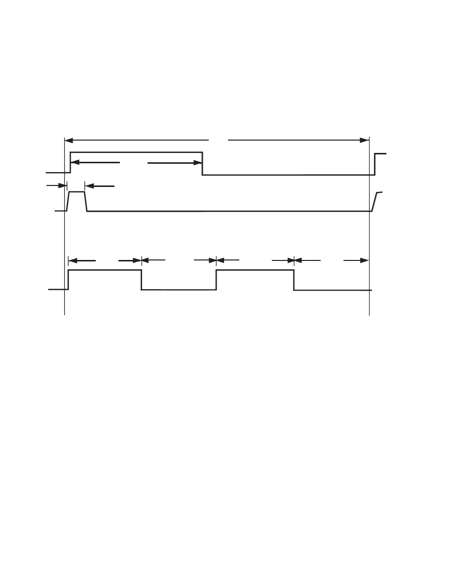
With respect to switching output signals, basically, only worry about signals that make an edge transition at a rate greater than
50 kHz (see Figure 1). If a pin changes its state at a rate of less than once per 100 instructions, this is acceptable because the
contribution from switching is negligible. If the pin toggles, and toggles back on the next instruction, and remains static for
100 instructions, it, too, is acceptable because it contains the same amount of energy as in the previous example.
10
µ
s
1
µ
s
5
µ
s
5
µ
s
5
µ
s
5
µ
s
100-kHz Clock Function May Need to Filter
No need to Filter
20
µ
s
Figure 1. Signals Below 50 kHz Are Not EMI Concerns
1.4 Basic Loops
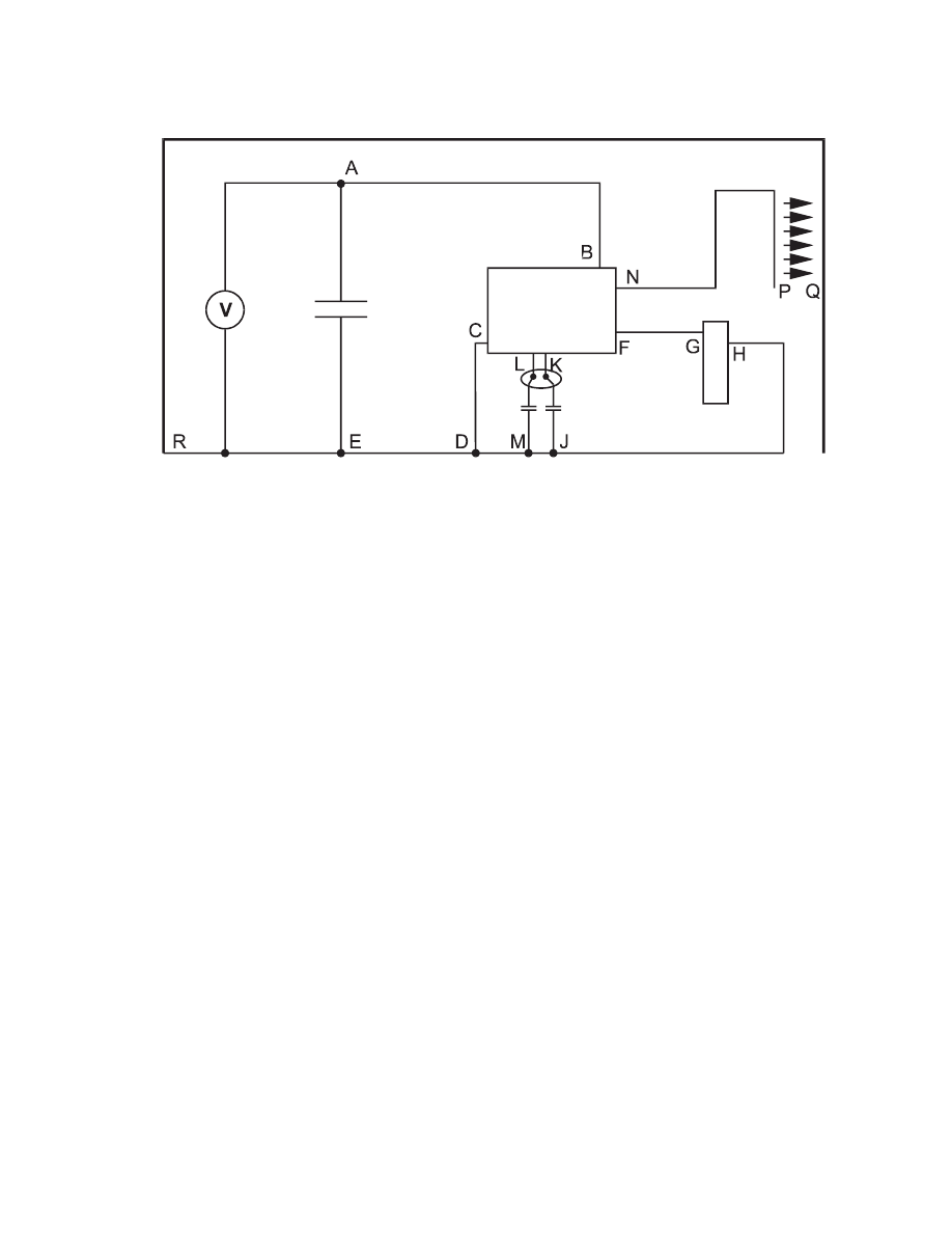
Every edge transition that is sent from the microcomputer to another chip is a current pulse. The current pulse goes to the
receiving device, exits through that device’s ground pin, then returns via the ground traces, to the ground pin of the
microcomputer (see Figure 2). The pulse does not exit the ground lead of the receiving device and return to the battery, but
travels in a loop to where it originates. Loops exist everywhere. Any noise voltage and its associated current travels the path(s)
of lowest impedance back to the place where it was generated. This is a very powerful concept, because it allows you to mitigate
noise propagation by controlling the shape and impedance of the return path.
A loop can be a signal and its return path, the bypassing loop between power and ground and the active devices inside the
microcomputer, the oscillator crystal and its driver in the microcomputer, as well as the loop from the power supply or voltage
regulator to the bypassing capacitors. Other more difficult loops are actually ambient field loops. For example, the crystal itself
radiates energy that can be coupled into a wire running nearby. Then, the wire contains noise that tries to get back to the crystal
loop. That may involve a very long and convoluted path, which serves as another antenna for noise from the crystal.
3
Internal Radiation Loop NP, Radiates to Q, Q-R-D-C
Xtal loop: K-J-M-L
Shield
Microcomputer
Bypass loop: A-B-C-D-E
Signal loop: F-G-H-D-C
Figure 2. Examples of Loops
1.4.1 Proportionality of Loops and Dipoles
Loops and dipoles are antennas. Their radiating efficiency increases up to 1/4 wavelength
(λ)
of the frequency of interest.
Geometrically, that means, in the case of a loop, that the larger the laid-out area of the loop, the stronger the radiation until one
or both legs of the loop reach 1/4 wavelength. In the dipole, the longer the antenna, the more radiation, until the length of the
antenna reaches 1/4 wavelength. At 1 MHz, 1/4
λ
= 75 m. At 300 MHz, 1/4
λ
= 25 cm, or about 10 inches.
1.5 Differential vs Common Mode
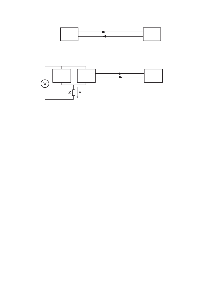
Differential-mode noise is the noise of a signal as it travels down its trace to the receiving device, then back along the return
path (see Figure 3). There is a differential voltage between the two wires. This is the type of noise that every signal must make
in order to do its job. Make sure there is no more noise than needed to get the job done, in terms of both frequency content (rise
and fall times) and the magnitude of the current. In common mode, a voltage travels down both the signal and return lines at
the same time. There is no differential between the signal and its return. The voltage is caused by an impedance that is common
to both the signal and the return. Common impedance noise is the most common source of noise in most microcomputer-based
systems that are not using external memories.
4
Signal
Source
Differential-mode noise is the ‘‘noise” voltage when a signal travels to its lead and returns. An
output switching is an example of differential-mode noise.
Load
Common-mode noise is the noise voltage that travels down both the signal and return
caused by a voltage drop across a shared impedance. Ground bounce on outputs is an
example of common-mode noise.
Current from the second signal source causes a drop across this
impedance, which causes a voltage on both signal and return.
Signal
Source
Signal
Source
Load
Return
Signal
Return
Signal
Figure 3. Differential-Mode vs Common-Mode Noise
2 Board Layout
2.1 Grounds and Power
The only non-dc current that should flow in the power routing of the PCB is the current required to replenish the bypassing
capacitor. High-frequency current used inside the microcomputer that is switched on the input clock edges should come from
the bypassing capacitors, not from the power supply.
2.1.1 Inductance
Inductance increases with increasing length, and decreases (at a slower rate) with increasing width of the conductor. In power
routing, the inductance makes voltage drops that radiate and propagate.
Because it is not desirable for any trace to radiate RF energy, any trace carrying RF energy should be as low an inductance as
possible:
•
On a two-layer board, for both power and ground, the length-to-width ratio should not exceed 3:1 for any traces
between the IC and the voltage source.
•
Power and ground should be run directly over each other, which reduces impedance and minimizes loop area.
2.1.2 Two-Layer vs Four-Layer Boards
A two-layer board can achieve 95% of the effectiveness of a four-layer board by emulating what makes a four-layer board
better:
•
Make an extra effort to route ground underneath power.
•
Grid power and ground, but be careful not to create unneeded common impedance connections or to violate an
intended isolation, such as between high-power and digital grounds. See section 2.2.3, Gridding to Create Planes.
•
Route returns for direct connections to the processor I/Os directly under the signal trace. Gridding is a
space-effective way of doing this. See section 2.2.3, Gridding to Create Planes.
•
Under the microcomputer, build a solid plane for ground that bypassing components and the oscillator loop can be
tied to. Tie this ground to the ground pin and the power-supply bypass capacitor. This is called a microcomputer
ground, which is discussed in section 2.1.3.
5
2.1.3 Microcomputer Grounds in One- and Two-Layer Designs
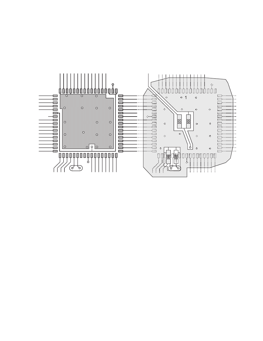
A microcomputer ground is a ground area on the bottom layer underneath the microcomputer that becomes a ground island
for the noise made by the microcomputer. This area should extend about 1/4 inch outside the outline of the device and tie to
the microprocessor ground. Ground connections for the power-supply bypassing capacitors and any bypassing capacitors on
the pins also should tie to this ground. Additionally, the ground area should extend out and around the through holes for the
oscillator leads, and the bypass capacitors tied in to provide the smallest possible loop area when viewed from the top. See
Figure 4 for an example.
ECP88
Top Side
Bottom Side
OSC
Capacitors
Ferrite
Bead
VCC Bypass
Capacitors
Figure 4. Microcomputer Ground
The topside traces are shown in dotted line form on the bottom side diagram for alignment purposes. Notice how the oscillator
capacitors lay back over the traces between the device and the crystal. This eliminates loop area. The same is true for the
placement of the ferrite bead and V
cc
bypass capacitor, being centrally located with the main power lead running almost directly
under the lead finger for the ground.
2.1.4 Signal Return Grounds
As mentioned previously in section 1.4, a loop is made by a signal, and the ground return path from the receiver device back
to the signal source. Signal return paths present the most difficult design problem in PCB layout.
It would be difficult to route a ground return underneath each trace connected to a signal pin on the microcomputer. But, this
is exactly what the ground plane of a four-layer board does. No matter where the traces run, there is always a ground return
path running underneath it.
The closest approximation to having a ground plane in a two-layer board comes from gridding the ground, as described in
section 2.2.3. As stated previously, radiation from the signal traces is the primary concern. Reducing the loop area by routing
the return for the signal underneath the signal trace is most effective way of dealing with this problem. Therefore, creating a
ground grid is the most important thing to do (after floor planning) in laying out the PCB.
2.1.5 Analog vs Digital vs High Power
Digital ground and power carry the RF energy that needs to be contained, so it is best to isolate it from any other power and
ground, either analog, high power, or other unrelated trace. If noise from the microcomputer or any other circuit gets on an
isolated ground, it can be returned by careful placement of a small RF capacitor in the 470 – 1000 pF range. Choosing the
location of the capacitor is by trial and error, and is best done in the screen room.
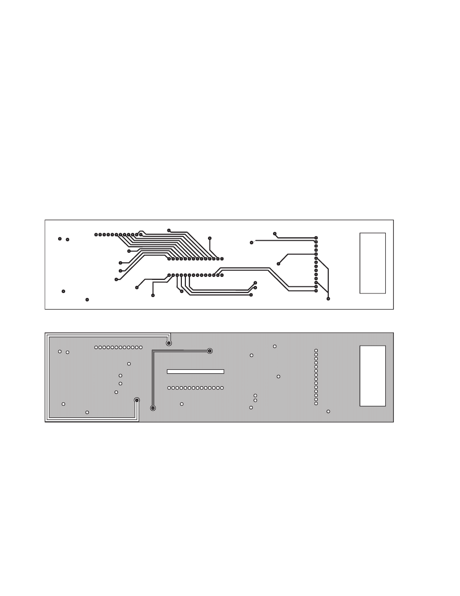
6
2.1.6 Analog Power-Supply Pins and Analog Reference Voltages
The reference voltage of an analog-to-digital (A/D) converter integrated into a microcomputer does supply a very small amount
of clocked current; however, it is not enough to be concerned about from a noise-emissions standpoint. Most applications have
the analog V
ss
/V
cc
tied to the digital V
ss1
/V
cc1
pins, which does not change significantly the noise characteristics of the A/D
nor the radiated emissions, provided the power distribution is built to guidelines in sections 2.1.1 through 2.1.4.
2.1.7
Power Plane Do’s and Don’ts for Four-Layer Boards
The reasons for reduced noise from four-layer boards were mentioned in section 2.1.2. The following guidelines should
maintain the advantages gained in the four-layer board.
•
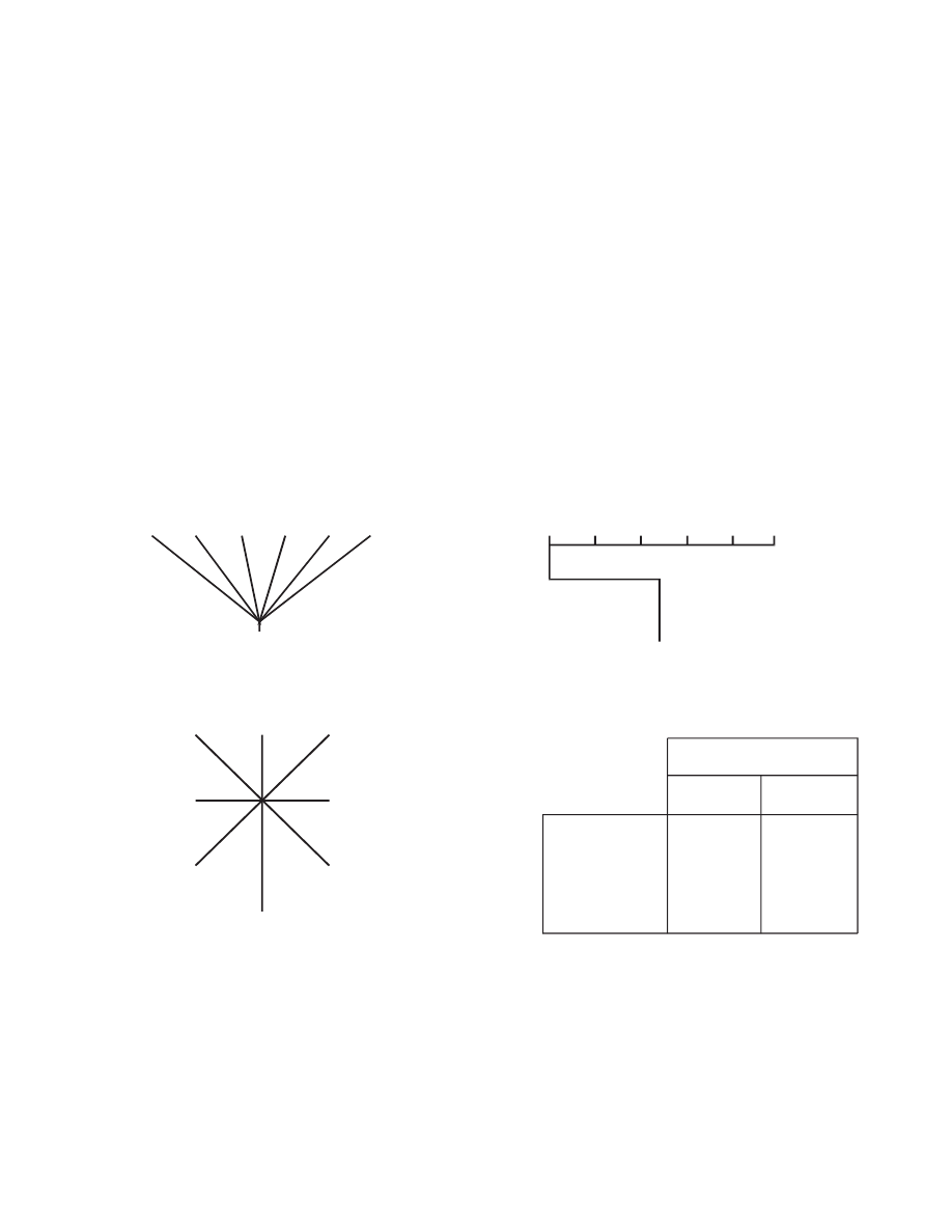
Pay utmost attention to how the holes and cutouts in the planes are done. They break up the plane and, therefore,
cause increases in loop areas (see A and B in Figure 5).
•
Avoid buried traces in the ground plane. If you have to use them, put them in the +V plane.
•
When making through holes for 100-mil-center-spacing leads in the plane, place a small trace between each pin.
Breaking up the plane with a row of holes is much better than having a long slot (see C and D in Figure 5).
•
When splitting up the ground plane to make, for example, a digital and power ground, make sure that the signals
connected to the microcomputer are still located entirely over the digital ground. Extending signal traces beyond
the power ground hurts because the power ground does not work to reduce the loop area for digital noise signals.
B
A
C
D
Ground Plane
A
POOR – Buried trace cuts ground plane into two parts
C
POOR – Slot formed by 100-mil spacing cuts up
ground plane and focuses slot antenna radiation into
that connection
B
BETTER – Buried trace around the perimeter
Best solution is no trace at all in the ground plane
D
BETTER – Ground plane extends between 100-mil
centers
Figure 5. Layout Considerations
7
2.2 Power Distribution for Two-Layer Boards
2.2.1 Single-Point vs Multipoint Distribution
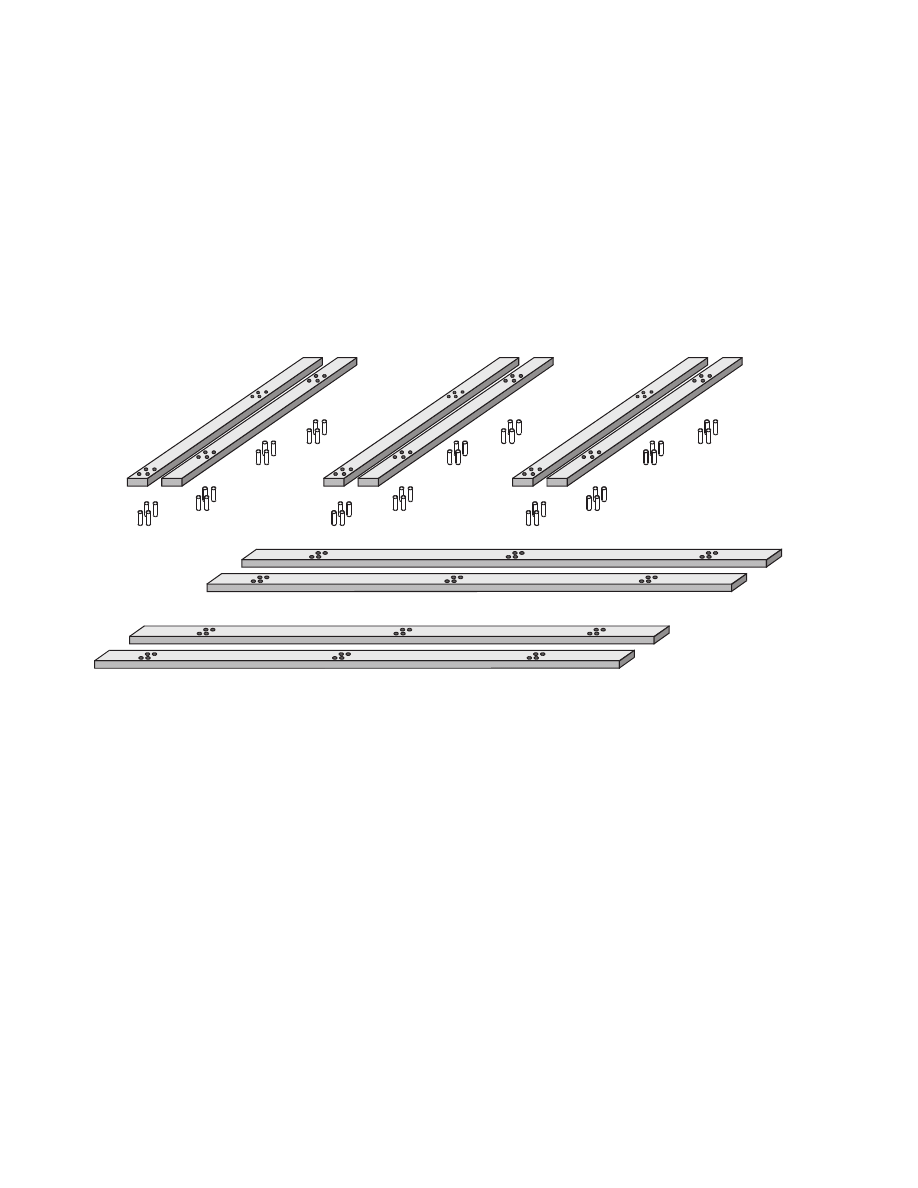
In a true single-point power-distribution system, each active component has its own separate power and ground, and these
traces would remain separate until they meet at a single reference point. In multipoint systems, the connections are made in
a daisy-chain fashion, so there are multiple 0-V reference points. It is clear that multipoint systems have the potential for
common impedance coupling. While implementing a single-point system may be impossible, a combination of single point
for devices generating RF and multipoint for everything else serves to reduce noise. The best scheme possible has a single point
that ties together the regulator ground, microcomputer ground, battery negative, and chassis or shield (see Figure 6).
2.2.2 Star Distribution
Star distribution is much like single point. It looks like all points reference the same fixed point, which is located centrally,
by about the same length of traces. Additionally, that same reference point may be attached, via a large single trace, to its source,
which is not centrally located. Therefore, the major differences to single point are:
•
The single reference point on a star can be a longer trace, instead of a point
•
The point where the separate traces begin is near the center of the board, and each trace goes in its own direction,
with the resulting trace length equal to that of all the others.
•
The star is best applied to something like a system clock in a high-speed computer board. The signal originates on
the edge connector and proceeds to the center of the board, where it then splits and goes to each place it is needed.
Since it effectively originates at the center of the board, the delay in the signal from one area of the board to another
is minimal. The name star sometimes is used to refer to single point, making the above clarification necessary.
Source
Single Point
USER USER USER USER USER USER
USER
USER
USER
USER
USER
USER
USER
Source ‘‘Star”
Source
Multipoint
USER USER
USER USER USER USER
Single Point
Star
Multipoint
O.K.
Best
Best
O.K.
Worst
Worst
Power
Signal
Trace Type
Figure 6. Power Distribution
2.2.3 Gridding to Create Planes
Gridding is the most critical design technique for two-layer boards. Much like a power utility grid, gridding is a network of
orthogonal connections between traces carrying ground. It effectively creates a ground plane, which provides the same noise
reduction as on four-layer boards. It serves two purposes:
•
Emulates the ground plane of a four-layer board by providing a ground return path under each of the signal traces
•
Lowers the impedance between the microcomputer and the voltage regulation
8
Gridding is done by expanding any ground traces and using ground-fill patterns to create a network of connections to ground
across the PCB. For example, a PCB has most of the topside traces running vertically and most of the bottom traces running
horizontally (see Figure 7). This already is working against having the return run directly under signal. First, every ground trace
is expanded to fill up as much of the empty PCB space as possible. Then, all the remaining empty space is filled with ground.
Place through holes where top-side traces cross bottom-side traces. Then do the same to the ground-fill patterns. Ground-fill
patterns make a better contribution to the grid if they are tied to ground at both ends. A ground-fill-pattern geometry connected
at only one point is just a ground shield, but if connected at two or more points, it becomes a conductor, and, therefore, becomes
a contributor in the grid.
•
Grid as much as possible on a two-layer board. Look for places where small changes in the layout would allow
another connection to be made in the grid.
•
Use as many through holes as can physically fit.
•
Lines do not have to be orthogonal, or of the same width.
Upper-layer power traces
Lower-layer power traces
GND
GND
GND
+V
+V
+V
GND
+V
GND
+V
Vias
Figure 7. Gridding Power Traces on Two-Layer Boards
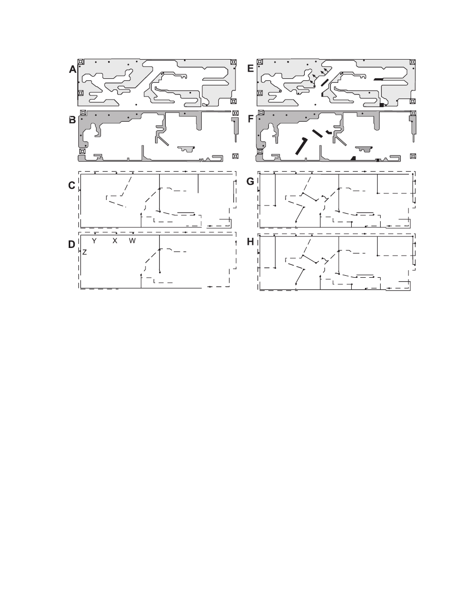
An example of gridding ground only to achieve the effect of a ground plane is shown in Figure 8. Note how the changes made
in order to implement this were minor, indicating how a small effort can have a large payback.
9
Figure 8. Gridding of Ground Fills and Traces to Form a Ground Plane
In the example in Figure 8, A and B represent the top and bottom sides, respectively, of a simple two-layer board. The +V traces
and all interconnects have been deleted, leaving only the ground fill and ground traces, along with the vias between the front
and back. Figure 8C is a simple stick diagram of the ground routing for the board. Each stick, or leg, represents the path of the
ground conductor, as if the conductor has been shrunk down to a minimum-width trace. The top-side traces are represented
by the dashed line, and the bottom-side traces by the solid line. It is easy to see in this diagram that most traces are dead ends.
Most traces are connected at only one end. In Figure 8D, most of the single-ended traces have been removed. The result is a
sparsely connected pattern that represents how ground is routed over the entire board. Excluding points W, X, Y, and Z in
Figure 8D, there is only one path between any two points anywhere on the routing.
In Figures 8E, 8F, 8G, and 8H, the design has been modified very slightly, to achieve a gridded ground. In Figures 8E and 8F,
the addition of some traces, shown in solid black, and slightly moving some geometries, as indicated by the arrows, has created
an extensive network of interconnections that creates the desired grid. This is shown by the stick diagram of ground in
Figure 8G. Closing the gaps around the mounting holes also contributes to the network. No longer are whole traces connected
at only one end. Now, they connect at both ends, and form a more complete conductor. Figure 8H shows the density of the grid,
which contrasts to the openness of Figure 8D. Also, notice how, in Figure 8H, no traces are dropped because they connect only
at one end. Only one trace has this problem, and it is part of a geometry already connected in three other locations. This
interconnected network is the goal of gridding ground. The result is nearly as effective as an actual ground plane.
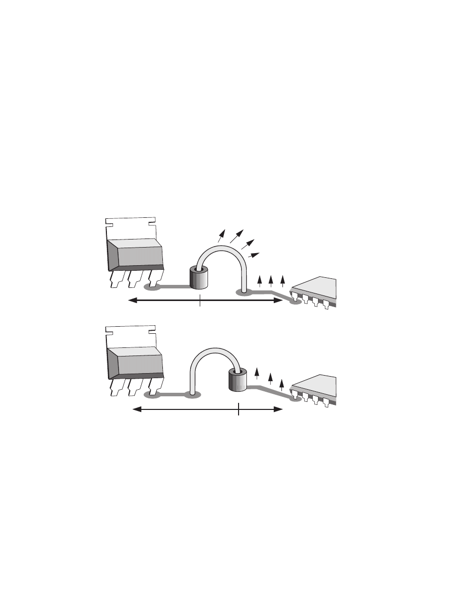
2.2.4 Bypassing and Ferrite Beads
Bypassing between the +V and ground at the microcomputer is critical because the intent is for the capacitance to supply the
current used in the device for switching. If the current is not available in the bypassing loop, because of too much inductance,
the laws of physics say that the current should come to the lowest impedance, which then is from the leads connecting to the
power supply. The distributed capacitance of the power routing becomes the source for the higher frequencies. Thus, the ferrite
bead blocks the sourcing of RF current from the power line connection, forcing the microcomputer to live off the current
available inside the ferrite bead.
10
It is of the utmost importance to realize, and always keep in mind, that the power-routing purpose is only to replenish the charge
in the bypassing capacitor, and that the bypassing capacitor should supply all currents at or above the oscillator frequency.
Keeping RF off the power distribution traces is accomplished using these measures (see Figure 9):
•
Use a ferrite bead and a bypassing capacitor (0.1
µ
F or 0.01
µ
F), placing the capacitors inside the ferrite bead. Place
a 1000-pF capacitor outside the ferrite bead, creating a PI filter. The ground connection for this capacitor should
be the microground. However, if there is a lot of noise on this point, the capacitor could couple that noise back onto
the +V line.
•
The ferrite bead is used only on +V, not on ground. If a through-hole ferrite bead is used, it is mounted with the
exposed lead connected to +V.
•
Apply the 3:1 length-to-width rule for traces in the bypassing loop, to minimize impedance in this high-frequency
path.
•
Make the bypassing loops as small as possible in area and length. When tying the bypass capacitors for the oscillator
or +V supply, try to extend the microcomputer ground rather than running a trace. Try to run any trace back over
(or under) any other segment of the loop to reduce the radiating area when viewed from the top of the board.
•
It is acceptable and beneficial to use ferrite beads and the same bypassing values on four-layer boards. The 1000-pF
capacitor may not be needed on four-layer boards, but it should be drawn in the initial design, and deleted later if
screen-room testing shows that it is not needed.
Quiet Side
Noisy Side
Quiet side does not radiate.
Noisy side radiates
Quiet Side
Noisy Side
Figure 9. Ferrite-Bead Placement Closest to the Noise Source

11
2.2.5 Keeping Noise Close to the Chip
The following applies to pins that are used for simple digital I/O, not for pins used in the memory-expansion bus. The goal
here is not so much to reduce the noise of the edge switching, but to mute the noise of the clock glitches when the pin is static.
Noise on the pins is coupled internal to the device through many paths that can change as the pin function changes. For example,
the input pin in a keyboard scan has capacitively coupled noise from both the substrate and the power rails. Also, because it
is high impedance, any ambient fields couple efficiently. When the key is pushed, the pin has a new set of noise sources because
the signal line’s impedance has changed. Thus, it is difficult to effectively develop a matrix of all possibilities; therefore, the
following is recommended:
•
Put a 50 –100-
Ω
resistor in series with every output pin, and 35 – 50-
Ω
resistor on every input pin. If the system
design calls for higher series resistance, use that value. Higher resistances are better for outputs, but usually do not
improve characteristics of inputs. Place the resistor as close as possible to the microcomputer, overlapping the
microcomputer ground if possible.
•
Bypass any pin on the microcomputer to ground using a 1000-pF capacitor, provided the edge rate needed for the
signal line is not faster than 100 ns. On outputs and pins that the system uses for both input and output, ground for
the capacitor should be the microcomputer ground. The other end of the capacitor should be tied to the receiver side,
not the microcomputer side, of the series resistor. Placing the capacitor inside the resistor makes the load seen by
the microcomputer look like a short when it switches, which is not desirable. If adding the capacitor has to be traded
off against placing the series resistor, because of space limitations, place only the resistor.
•
On pins used for input only, place the capacitor inside, on the microcomputer side, of the resistor to reduce the loop
area. Then, high frequencies originating in the microcomputer on the pin see less impedance to ground through the
capacitor than through the resistor.
•
Resets and interrupts are special functions, thus care must be taken not to reduce functionality.
•
Do not apply any of the above remedies to oscillator pins. If proper spacing between the oscillator components and
other unrelated components and traces is maintained, there should not be a need for oscillator signal conditioning.
•
Unused pins should be configured as inputs and tied directly to the microcomputer ground. It is recommended that
the watchdog be enabled to correct the unlikely event in which a device is disturbed, loses its program counter, and
executes code to make the input become an output with a high level.
These rules take up space and add components, and so are not well accepted in production. The goal is to implement all rules
on all I/O pins, but if that is not possible, then rank order the candidates least likely to cause noise and remove the application
of these rules one pin at a time.
Filtering priorities from most needed to least needed are:
•
Signals leaving the enclosure (see section 3.3, Cables and Bypassing to the Shield)
•
Signals leaving the PCB to other boards inside the enclosure
•
Signals staying on the PCB with high-impedance loads (i.e., driving another MOS input or open circuit)
•
Pins of parallel I/O port designed to support high-speed data transfer, e.g., between the microcomputer and an
external memory, need filtering over the remaining I/O pins, because of their faster rise and fall times.
When the design is complete and first prototypes are built, an hour or two in the screen room removing each of the filtering
components one at a time, identifies which are or are not needed to get the desired EMI level.
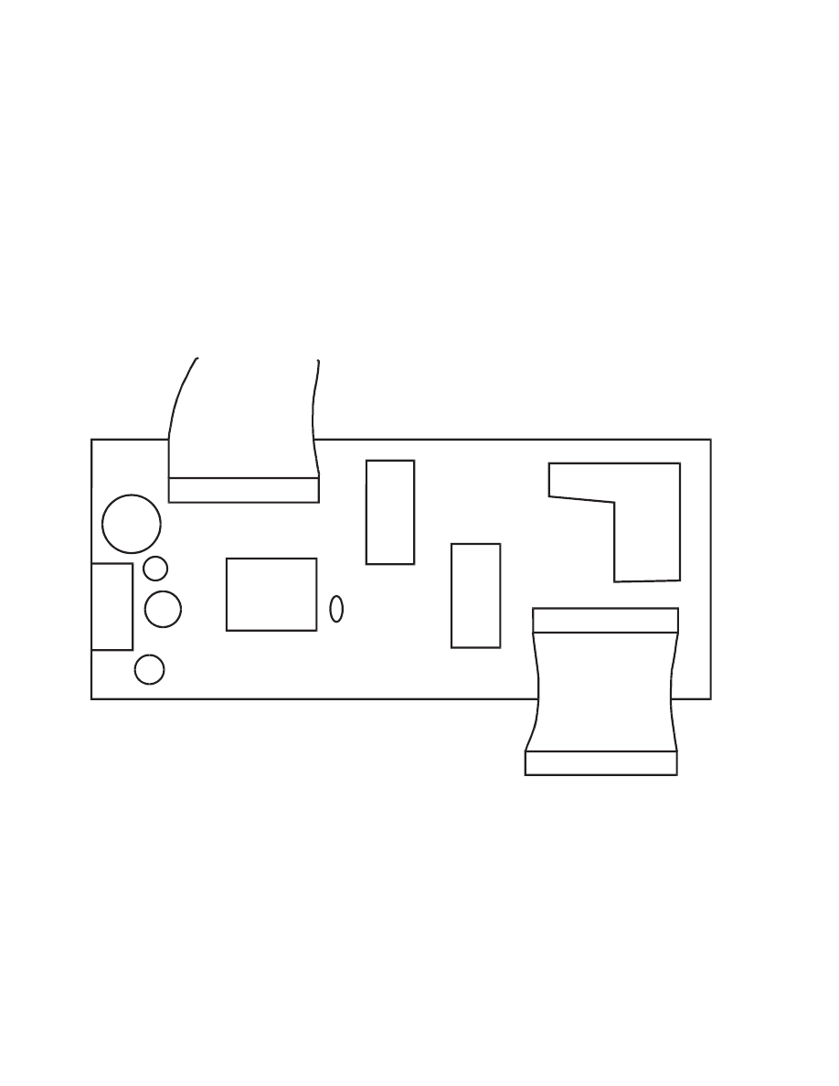
12
2.3 Board Zoning
Board zoning has the same basic meaning as board floor planning, which is the process of defining the general location of
components on the blank PCB before drawing in any traces. Board zoning goes a little bit further in that it includes the process
of placing like functions on a board in the same general area, as opposed to mixing them together (see Figure 10). High-speed
logic, including micros, are placed close to the power supply, with slower components located farther away, and analog
components even farther still. With this arrangement, the high-speed logic has less chance to pollute other signal traces. It is
especially important that oscillator tank loops be located away from analog circuits, low-speed signals, and connectors. This
applies both to the board, and the space inside the box containing the board. Do not design in cable assemblies that fold over
the oscillator or the microcomputer after final assembly, because they can pick up noise and carry it elsewhere.
In prioritizing component placement, the most important things to do in PCB design are:
•
Locate the microcomputer next to the voltage regulator, and the voltage regulator next to where V
Batt
enters the
board.
•
Built a gridded or solid ground between the three (forming a single-point ground), and tie the shield at that point.
XT
AL
Chassis harness, microcomputer regulator are all in the same area. Wide
ground fields interconnect all three, forming single-point ground reference.
Front Panel
CHASSIS HARNESS
ANALOG
Microcomputer
V
R
E
G
Figure 10.
Board Zoning
13
2.4 Signal Traces
2.4.1 Capacitive and Inductive Crosstalk
Capacitive and inductive crosstalk occur between traces that run parallel for even a short distance. In capacitive coupling, a
rising edge on the source causes a rising edge on the victim. In inductive coupling, the voltage change on the victim is in the
opposite direction as the changing edge on the source. Most instances of crosstalk are capacitive. The amount of noise on the
victim is proportional to the parallel distance, the frequency, the amplitude of the voltage swing on the source, and the
impedance of the victim, and inversely proportional to the separation distance. Measures that reduce crosstalk are:
•
Keeping RF-noise-carrying traces that are connected to the microcomputer away from other signals so they do not
pick up noise.
•
Signals that may become victims of noise should have their return ground run underneath them, which serves to
reduce their impedance, thus reducing the noise voltage and any radiating area.
•
Never run noisy traces on the outside edge of the board.
•
If possible, group a number of noisy traces together surrounded by ground traces.
•
Keep non-noisy traces away from areas on the board were they could pick up noise, such as connectors, oscillator
circuits, relays, and relay drivers.
Most EMI-related crosstalk problems center around the crystal, when the victim is located too close. No unrelated components
should be closer than 1 inch to the crystal.
2.4.2 Antenna Factor Length Rules
Normally, for Federal Communication Commission (FCC) limits, trace length becomes important when it is greater than 1/10
of the wavelength. For military standard limits, that number becomes 1/20 to 1/30 of the wavelength. For automotive and
consumer two-layer boards, 1/50 of the wavelength begins to be critical, particularly in unshielded applications. That says
traces longer than 4 inches can be a problem for FM-band noise. In these cases, some form of termination is recommended
to prevent ringing.
2.4.3 Series Termination, Transmission Lines
The main purpose of termination is to provide critical damping to achieve the highest possible data transmission rates with the
least-possible overshoot. When applied to most microcontroller systems, however, the focus changes to taking out as much
total differential-mode noise as possible while allowing system functionality. Below is a table of different methods of
termination and the main characteristics of each method.
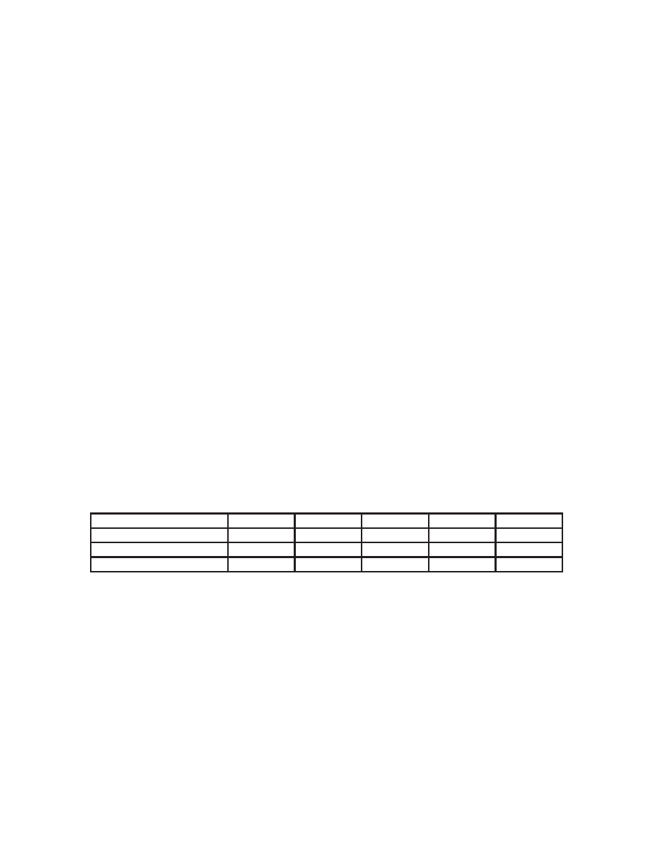
Table 1. Termination Characteristics
Parallel
Thevenin
Series
AC
Active
Power dissipation
high
high
low
medium
medium
Number of components
1
2
1
2
1
Adds delay
no
no
yes
no
no
Note that CMOS is an under-damped technology, which means that you always have to be on guard for ringing and overshoot.
Use some form of termination if any of the following conditions are present:
•
A signal trace is more than 1 foot long.
•
A signal goes to a cable that leaves the shielded enclosure.
•
Any ringing is present.
Series resistance is an inexpensive solution to termination and ringing problems, and is the preferred method for
microcomputer-based systems where minimizing the differential-mode noise is also a concern.
14
2.4.4 Impedance Matching at Inputs
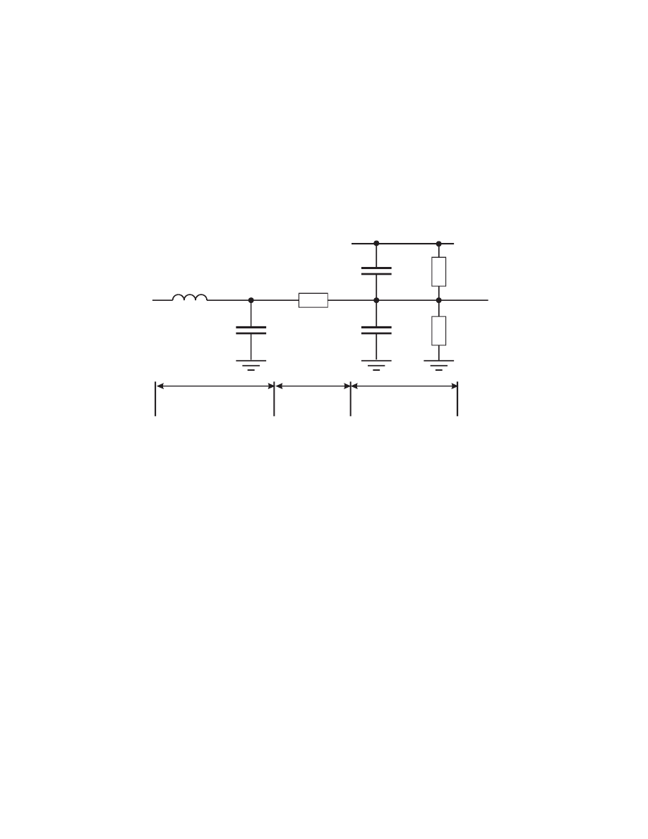
The input to a CMOS device looks like a series inductance of about 5 – 40 nH, which leads to about 5 pF in parallel, with about
5 M
Ω
to the grounded substrate (see Figure 11). This is a very high impedance, and can lead to lots of ringing and other noise
if the device driving the input is not matched in some fashion to the higher impedance. This is the complement of the situation
of section 2.4.3, where attention is paid to the microcomputer’s output because of the under-damped nature of the load it drives.
Here, the microcomputer is the under-damped load, and ringing and overshoot are real possibilities. More than likely, some
form of termination will be required, and again, the series resistance is the most likely solution. Resistance placed at the driver
increases the output impedance, as seen by the trace and the input pin, thus matching the high impedance of the input.
If the input is connected to an open trace, such as the open line to a switch, a pullup or pulldown resistor is recommended. While
this increases the amount of current switched when the input is activated, it reduces the impedance at all other times. This
reduces the trace’s chances of being a victim of coupled noise.
Device Pin
Connects
to PCB
2 – 20
Ω
1 – 2 pF
5 – 40 nH
1 – 5 pF
1 – 5 pF
>1 M
Ω
>1 M
Ω
Vdd
Signal
Goes into
Device
Input and
Bond Wire
Input Gate
Lead Finger
and Bond Wire
Figure 11. MOS Buffer Simplified Schematic
2.5 Cables and Connectors
A well-designed two-layer board, and most four-layer boards, have minimal radiation. The problem at the system level is the
radiation due to cables interconnecting the PCB with any off-board support function, other processor, or display and keypad
PCBs. Because usually there is only one ground wire between boards, that one inductive wire has to return all of the RF energy
carried onto the second PCB by the other wires. If there is any impedance in the single ground wire, a portion of the RF energy
does not return to the microcomputer’s PCB via the ground wire, but rather through a radiated path. The energy radiates off
the second board and couple back to the first, but, during the process, that radiation also can add noise in other locations in
the system, as well as become direct radiation measured in the screen room. The key corrective action is to ensure the conducted
path for the return has a very low RF impedance.
2.5.1 Differential-Mode and Common-Mode Noise
Common-mode noise is a big problem in cables, but the fault does not lie in the cable, it lies in the connections on the board
that the signals and returns tie to that form the common impedance. Common-mode noise is corrected either at the source, by
reducing the impedance of the common node, or reduced by placing a ferrite bead around the entire cable.
Differential-mode noise (the useful noise of an edge transition) should first be reduced to the maximum (slowest) allowable
rise and fall times and should occur at only the minimum needed frequency. The noise radiated is due to the loop of the signal
and its return. This loop is minimized by having as many returns as possible and by twisting each signal and return pair. The
latter causes field cancellation at some distance away, in the same manner as routing power over ground.
2.5.2 Crosstalk Model
Crosstalk in a cable is the same as in the PCB. Noise is coupled from the source onto quiet victim signals. Therefore, run
clocking or other high-speed wires twisted with their own separate return. Crosstalk is a problem in cables over 2-meters long,
and can be a problem in cables as short as 6 inches.

15
2.5.3 Number of Returns
It is common practice in the computer industry to have at least one ground for every nine other signal lines in a cable or harness.
With higher speeds, this ratio is moving toward 1:5. These higher speeds are not limited to data rates, but also to harmonic
content. Use these guidelines in designing signal and return lines:
•
The best practice is to have one ground return for each signal in the cable, as a twisted pair.
•
Never run less than one ground return for every nine signal lines, even if it is just the jumper cable to the front-panel
display in a completely sealed metal box.
•
If the cable is over one foot long, it should have one ground return line for four signal lines.
•
When possible, there should be a solid metal bracket, used as a mechanical brace, soldered between the two boards,
to serve as a mounting bracket and as a robust RF ground return.
2.5.4 I/O Recommendations for Off-PCB Signals
The PCB should have a large ground area tied to the enclosure shield that serves as the ground for the bypassing capacitors
on each of the wires entering or leaving the enclosure. These capacitors provide final filtering of microcomputer noise, but
also are intended to filter to the shield any noise picked up on the cable outside the box. See section 3.3, Cables and Bypassing
to the Shield.
2.5.5 Keeping Noise and Electrostatic Discharge (ESD) Out
Noise and ESD incident on the cable are intended to pass through the bypass capacitor at the cable on the PCB and out to the
shield (chassis). Therefore, the ground from the capacitor to shield should be wide (3:1) and bonded securely to the shield,
preferably by two or more screws. The bypass capacitor value should be less than 1000 pF, so the effective series resistance
(ESR) is minimum in the 50 – 500-MHz range. Lead length of axial devices would be a factor in the ESR, so surface-mount
components are preferred.
2.6 Other Layout Issues
2.6.1 Front-Panel PCB with Keypad and Display in Automotive and Consumer Applications
In multi-PCB applications, a front-panel PCB, which carries the display and the keyboard, is part of the shielding enclosure.
It also can be a source of emissions. The goal here is to make the ground return for the noise of the microcomputer, and to create
an effective extension of the shield over the front of the box. This can be done by defining all lines on one side of the board
to run one way, and the other side to run at 90 degrees (see Figure 12). Then, interspersed among the signals for keyboard and
matrix, are the lines that make up two separate gridded ground planes: one that serves as the ground return and one that serves
as part of the shield. The latter should securely contact the chassis at each corner and every two inches along the edge. The
return ground plane should tie to the microcomputer’s ground plane, preferably using something heavy, like soldered-in metal
braces. This prevents the impedance between the controller and the front-panel PCB from being a major problem.
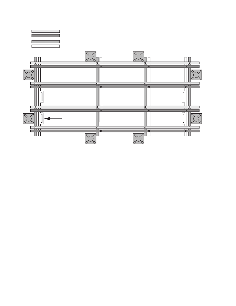
16
Front-Side Shield Ground
Front-Side Controller Ground
Back Shield Ground
Back-Side Controller Ground
Mounting bracket
solder point
Figure 12. Front-Panel Gridding to Form Two Ground Planes
2.6.2 Layout for Susceptibility
Susceptibility (called immunity in Europe) occurs as incident electric or magnetic fields couple onto signal traces. Because
the coupled signal is alternating current, the sine wave is superimposed on voltage already present on the trace. At the input
to a microcomputer, that voltage is rectified, and causes a dc offset voltage on the pin. When this dc voltage gets large enough
to shift the input away from the switching-point voltage, the intended switching function is no longer seen by the
microcomputer. If the input is the oscillator, the device suddenly has no clocks. If the input is reset, the device may go into reset
and stay there until the disturbing field is removed.
The physics of susceptibility are the same as for emissions, only applied in reverse. Large loop areas pick up more signal, just
as they would radiate more signal. Therefore, the things you do to keep a signal immune from radiation are the same as those
to keep it from radiating.
The most important pins for immunity are those that affect program control: the oscillator, reset, interrupts, and any input pins
used for program branching. Apply the same rules as for reducing radiation from these pins. By far, most susceptibility problems
are associated with the loop defined by the oscillator pins, the crystal, the crystal bypass capacitors, and the path between the
bypass-capacitor ground connection and the ground of the microcomputer.
Also, be careful of ground bounce (common impedance coupling) of circuits that may generate these more critical signals. If
the ground path has high impedance, it may cause the driving circuit’s reference voltage to shift, causing that input to the
microcomputer (RESET, OSC) to be outside the switching range of the microcomputer.
2.6.3 Autorouters
Autorouters for PCBs do not take any noise reduction actions; therefore, care should be taken in their use. Power and ground
routing, as well as signals that impact susceptibility, should be laid out by hand. Any signal with clocked data, such as low
address bits in a memory expansion bus, should be next. Only signals with switching rates below 50 kHz can be left safely to
the autorouter. Even then, every signal should be checked for EMI issues. Routing near the crystal, and the crystal and tank
circuit itself, should be checked. Finally, the ground traces should be gridded.

17
3
Shielding
3.1 How It Works
When an incident electric field traveling in the air hits a metal surface, the metal causes the penetrating field strength to
decrease. The metal causes the field to be replaced with conduction currents that flow in the metal close to the surface. A very
small (exponential decay) amount of the field does pass through, but for emissions, this is never a problem. The metal chassis
serves as a shield. The fields from all the radiating surfaces inside it are blocked and kept inside the box, with the only noise
coming from the cables or wires that enter or exit the box and from holes or slots made in the box.
If a metal enclosure is to be used, its shielding effect should be utilized. However, it is always better to reduce the noise inside
the box than to rely on the shielding effectiveness.
3.2 Grounding the Shield
The shield has the difficult job of providing a terminating or conducting surface for direct ESD hits, ambient fields, and internal
fields, as well as noise carried on the cables entering and exiting the chassis. To do this well, the shield should be thought of
as an RF conducting plane, with the least number of breaks and impedance’s between the source of the RF currents and the
ground reference point. The ground reference point should be the single point, as mentioned earlier, that ties together the
regulator ground, the microcomputer ground, and battery negative.
3.3 Cables and Bypassing to the Shield
The PCB should have a large separate ground area tied to the enclosure shield which serves as the ground for the I/O bypassing
capacitors (see Figure 13). These capacitors provide final filtering of system noise, but also are intended to filter noise picked
up on the cable outside the box. The value of the capacitor should be below 1000 pF, more likely about 470 pF. The connection
to the chassis is an RF path requiring 3:1 length to width.
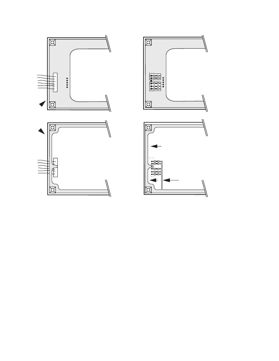
18
Large ground on both sides
reduces impedance, a good
starting point for the 0-V
reference point for the power
supply.
Narrow traces increase
impedance, which reduces
filtering effectiveness.
GOOD
BAD
Bottom Side
Top Side
SHIELD
Figure 13. Mounting Filter Capacitors for External I/Os
3.4 Slot Antennas: Cooling Slots and Seams
Slots antennas are formed by long thin gaps in the shielding material, such as at the seams between the two pieces of the box,
and at the front-panel interface. These slots are very effective radiators. It is important that some form of contact assurance
be used, such as dimpling, or using alternating fingers, to insure contact between the two surfaces. No slot should be more than
4 inches long. Cooling slots should not be used. For emissions reasons, only small round holes should be used if ventilation
is needed.
4 Summary
The design of systems that generate low electromagnetic interference is not a mystery, but requires application of well-known
engineering techniques. The design begins with the selection of semiconductor components that produce low electromagnetic
radiation. However, in many cases, other criteria, such as the required performance of the semiconductor component, may be
in contradiction with low interference. The main task is the design of a PCB that eliminates antennas that can radiate
electromagnetic energy. Even if this can be achieved sometimes, large loops of signal and corresponding ground-return lines
that carry high frequencies must be avoided. Therefore, a careful positioning of the integrated circuits is essential to achieve
short interconnect lines.
In the next step, a close ground grid is placed over the printed circuit board. This grid ensures that return lines are close to the
signal lines, thus keeping the effective antenna area small. A ground plane in a multilayer board provides this feature. By using
this technique, low electromagnetic emission can be achieved with low design effort. However, some cost-sensitive
applications allow two-layer PCBs only. Nevertheless, in this case, careful layout provides nearly the same performance as
a multilayer board.

19
Finally, filtering of critical lines, such as the supply line, ensures that high-frequency currents do not leave the PCB.
By applying the rules presented in this report, shielding of the total system is not required. Experience and careful work by
the design engineer are much more effective than sophisticated computer-aided design tools.
5 References
1.
Printed-Circuit-Board Layout for Improved Electromagnetic Compatibility, October 1996, Application Report,
literature number SDYA011.
2.
Electromagnetic Emission from Logic Circuits, November 1998, Application Report, literature number SZZA007.
3.
Texas Instruments Internet Web Page at http://www.ti.com
Wyszukiwarka
Podobne podstrony:
LOW EMI PCB DESIGN id 273292 Nieznany
Abolicja podatkowa id 50334 Nieznany (2)
4 LIDER MENEDZER id 37733 Nieznany (2)
katechezy MB id 233498 Nieznany
metro sciaga id 296943 Nieznany
perf id 354744 Nieznany
interbase id 92028 Nieznany
Mbaku id 289860 Nieznany
Probiotyki antybiotyki id 66316 Nieznany
miedziowanie cz 2 id 113259 Nieznany
LTC1729 id 273494 Nieznany
D11B7AOver0400 id 130434 Nieznany
analiza ryzyka bio id 61320 Nieznany
pedagogika ogolna id 353595 Nieznany
Misc3 id 302777 Nieznany
cw med 5 id 122239 Nieznany
D20031152Lj id 130579 Nieznany
więcej podobnych podstron