One Technology Way, P.O. Box 9106, Norwood. MA 02062-9106, U.S.A.
Tel: 617/329-4700
Fax: 617/326-8703
REV. 0
Information furnished by Analog Devices is believed to be accurate and
reliable. However, no responsibility is assumed by Analog Devices for its
use, nor for any infringements of patents or other rights of third parties
which may result from its use. No license is granted by implication or
otherwise under any patent or patent rights of Analog Devices.
a
High Speed, +5 V, 0.1
µ
F
CMOS RS-232 Drivers/Receivers
FEATURES
200 kB/s Transmission Rate
Small (0.1
µ
F) Charge Pump Capacitors
Single 5 V Power Supply
Meets All EIA-232-E and V.28 Specifications
Two Drivers and Two Receivers
On-Board DC-DC Converters
±
9 V Output Swing with +5 V Supply
±
30 V Receiver Input Levels
Pin Compatible with MAX222/MAX232A/MAX242
APPLICATIONS
Computers
Peripherals
Modems
Printers
Instruments
ORDERING GUIDE
Model
Temperature Range
Package Option
ADM222AN
–40
°
C to +85
°
C
N-18
ADM222AR
–40
°
C to +85
°
C
R-18W
ADM232AAN
–40
°
C to +85
°
C
N-16
ADM232AARN
–40
°
C to +85
°
C
R-16N
ADM232AARW
–40
°
C to +85
°
C
R-16W
ADM242AN
–40
°
C to +85
°
C
N-18
ADM242AR
–40
°
C to +85
°
C
R-18W
*
INTERNAL 400k
Ω
PULL-UP RESISTOR
ON EACH TTL/MOS INPUT
**
INTERNAL 5k
Ω
PULL-DOWN RESISTOR
ON EACH RS-232 INPUT
V
CC
+5V TO +10V
VOLTAGE DOUBLER
+5V TO –10V
VOLTAGE INVERTER
C1+
C1–
V+
V–
C2+
C2–
T1
ADM2xx
T2
R1
R2
0.1µF
0.1µF
0.1µF
GND
TTL/CMOS
OUTPUTS
R1
OUT
R2
OUT
T1
OUT
T2
OUT
R1
IN
R2
IN
T1
IN
T2
IN
TTL/CMOS
INPUTS
*
RS-232
OUTPUTS
RS-232
INPUTS
**
0.1µF
+5V INPUT
0.1µF
EN
SHDN
(ADM242)
(ADM222, ADM242)
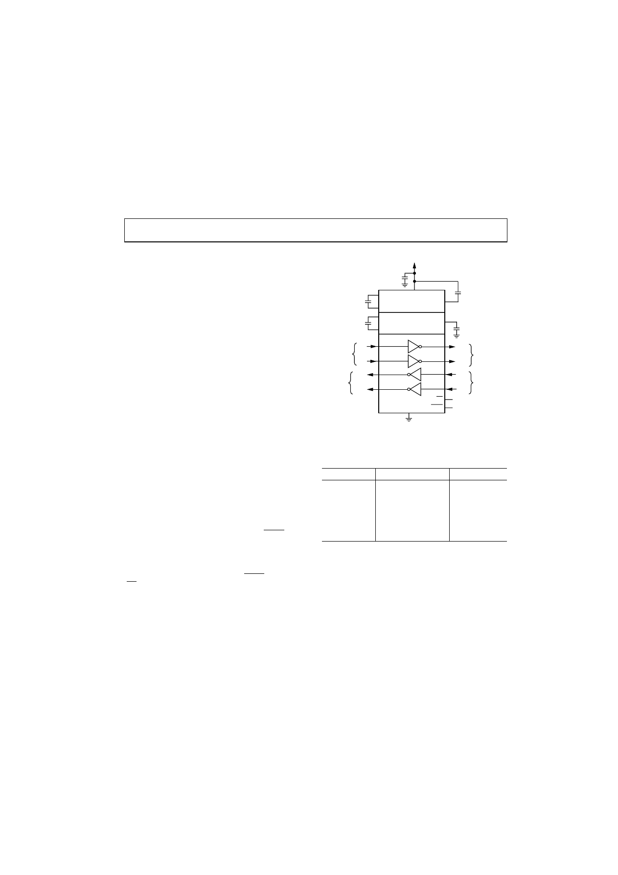
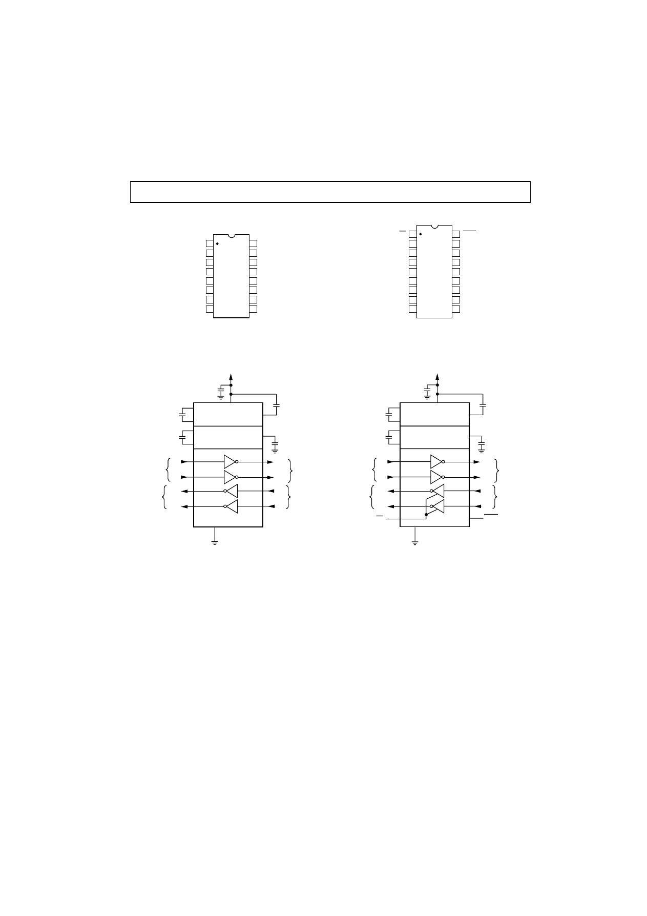
ADM222/ADM232A/ADM242*
FUNCTIONAL BLOCK DIAGRAM
GENERAL DESCRIPTION
The ADM222, ADM232A, ADM242 are a family of high speed
RS-232 line drivers/receivers offering transmission rates up to
200 kB/s. Operating from a single +5 V power supply, a highly
efficient on-chip charge pump using small (0.1
µ
F) external
capacitors allows RS-232 bipolar levels to be developed. Two
RS-232 drivers and two RS-232 receivers are provided on each
device.
The devices are fabricated on BiCMOS, an advanced mixed
technology process which combines low power CMOS with high
speed bipolar circuitry. This allows for transmission rates up to
200 kB/s yet minimizes the quiescent power supply current to
under 5 mA.
The ADM232A is a pin-compatible, high speed upgrade for the
AD232 and for the ADM232L. It is available in 16-pin DIP and
in both narrow and wide surface mount (SOIC) packages.
The ADM222 contains an additional shutdown (SHDN) func-
tion which may be used to disable the device thereby reducing
the supply current to 0.1
µ
A. During shutdown, all transmit/
receive functions are disabled. The ADM222 is available in
18-pin DIP and in a wide surface mount (SOIC) package.
The ADM242 combines both shutdown (SHDN) and enable
(EN) functions. The shutdown function reduces the supply
curent to 0.1 mA. During shutdown, the transmitters are
disabled but the receivers continue to operate normally. The
enable function allows the receiver outputs to be disabled
thereby facilitating sharing a common bus. The ADM242 is
available in 18-pin DIP and in a wide surface mount (SOIC)
package.
*Protected by U.S. Patent No. 5,237,209.
REV. 0
–2–
Parameter
Min
Typ
Max
Units
Test Conditions/Comments
RS-232 TRANSMITTERS
Output Voltage Swing
±
5
±
9
V
All Transmitter Outputs Loaded with
3 k
Ω
to Ground
Input Logic Threshold Low, V
INL
1.4
0.8
V
T
IN
Input Logic Threshold High, V
INH
2.0
1.4
V
T
IN
Logic Pullup Current
5
40
µ
A
T
IN
= 0 V
Data Rate
200
kB/s
Output Resistance
300
Ω
V
CC
= V+ = V– = 0 V, V
OUT
=
±
2 V
Output Short Circuit Current (Instantaneous)
±
7
±
22
mA
RS-232 RECEIVERS
RS-232 Input Voltage Range
–30
+30
V
RS-232 Input Threshold Low
0.8
1.3
V
RS-232 Input Threshold High
1.8
2.4
V
RS-232 Input Hysteresis
0.2
0.5
1.0
V
V
CC
= 5 V
RS-232 Input Resistance
3
5
7
k
Ω
TTL/CMOS Output Voltage Low, V
OL
0.2
0.4
V
I
OUT
= 3.2 mA
TTL/CMOS Output Voltage High, V
OH
3.5
V
I
OUT
= –1.0 mA
TTL/CMOS Output Short-Circuit Current
–2
–10
mA
Source Current (V
OUT
= GND)
TTL/CMOS Output Short-Circuit Current
10
30
mA
Sink Current (V
OUT
= V
CC
)
TTL/CMOS Output Leakage Current
±
0.05
±
10
µ
A
SHDN
= GND/EN = V
CC
0 V
≤
V
OUT
≤
V
CC
EN
Input Threshold Low, V
INL
1.4
0.8
V
EN
Input Threshold High, V
INH
2.0
1.4
V
POWER SUPPLY
Power Supply Current
4
8
mA
No Load
15
mA
3 k
Ω
Load on Both Outputs
Shutdown Power Supply Current
0.1
10
µ
A
SHDN
Input Leakage Current
±
1
µ
A
SHDN
Input Threshold Low, V
INL
1.4
0.8
V
SHDN
Input Threshold High, V
INH
2.0
1.4
V
AC CHARACTERISTICS
Transition Region Slew Rate
6
12
30
V/
µ
s
C
L
= 50 pF to 2500 pF, R
L
= 3 k
Ω
to 7 k
Ω
Measured from +3 V to –3 V or –3 V to +3 V
Transmitter Propagation Delay TTL to RS-232
0.7
3.5
µ
s
t
PHLT
0.7
3.5
µ
s
t
PLHT
Receiver Propagation Delay RS-232 to TTL
0.2
0.5
µ
s
t
PHLR
0.3
0.5
µ
s
t
PLHR
Receiver Output Enable Time
125
500
ns
t
ER
Receiver Output Disable Time
160
500
ns
t
DR
Transmitter Output Enable Time
250
µ
s
SHDN
Goes high
Transmitter Output Disable Time
3.5
µ
s
SHDN
Goes low
Transmitter + to – Propagation Delay Difference
300
ns
Receiver + to – Propagation Delay Difference
100
ns
Specifications subject to change without notice.
ADM222/ADM232A/ADM242–SPECIFICATIONS
(V
CC
= +5 V
±
10%, C1–C4 = 0.1
µ
F; all spec-
ifications T
MIN
to T
MAX
unless otherwise noted.)
ADM222/ADM232A/ADM242
REV. 0
–3–
ABSOLUTE MAXIMUM RATINGS
*
(
T
A
= +25˚C unless otherwise noted)
V
CC
. . . . . . . . . . . . . . . . . . . . . . . . . . . . . . . . . . . . . . . . . +6 V
V+ . . . . . . . . . . . . . . . . . . . . . . . . . . . . . (V
CC
– 0.3 V) to +13 V
V– . . . . . . . . . . . . . . . . . . . . . . . . . . . . . . . . . . +0.3 V to –13 V
Input Voltages
T
IN
. . . . . . . . . . . . . . . . . . . . . . . . . –0.3 V to (V
CC
+ 0.3 V)
R
IN
. . . . . . . . . . . . . . . . . . . . . . . . . . . . . . . . . . . . . .
±
30 V
Output Voltages
T
OUT
. . . . . . . . . . . . . . . . . . . . (V+, +0.3 V) to (V–, –0.3 V)
R
OUT
. . . . . . . . . . . . . . . . . . . . . . . . –0.3 V to (V
CC
+ 0.3 V)
Short Circuit Duration
T
OUT
. . . . . . . . . . . . . . . . . . . . . . . . . . . . . . . . . Continuous
Power Dissipation N-16 . . . . . . . . . . . . . . . . . . . . . . . 400 mW
(Derate 7.5 mW/
°
C above +70
°
C)
θ
JA
, Thermal Impedance . . . . . . . . . . . . . . . . . . . . . . 80
°
C/W
Power Dissipation R-16N . . . . . . . . . . . . . . . . . . . . . 400 mW
(Derate 7 mW/
°
C above +70
°
C)
θ
JA
, Thermal Impedance . . . . . . . . . . . . . . . . . . . . . . 80
°
C/W
Power Dissipation R-16W . . . . . . . . . . . . . . . . . . . . . 400 mW
(Derate 7 mW/
°
C above +70
°
C)
θ
JA
, Thermal Impedance . . . . . . . . . . . . . . . . . . . . . . 80
°
C/W
Power Dissipation N-18 . . . . . . . . . . . . . . . . . . . . . . . 400 mW
(Derate 7 mW/
°
C above +70
°
C)
θ
JA
, Thermal Impedance . . . . . . . . . . . . . . . . . . . . . . 80
°
C/W
Power Dissipation R-18W . . . . . . . . . . . . . . . . . . . . . 400 mW
(Derate 7 mW/
°
C above +70
°
C)
θ
JA
, Thermal Impedance . . . . . . . . . . . . . . . . . . . . . . 80
°
C/W
Operating Temperature Range
Industrial (A Version) . . . . . . . . . . . . . . . . –40
°
C to +85
°
C
Storage Temperature Range . . . . . . . . . . . . –65
°
C to +150
°
C
Lead Temperature (Soldering, 10 sec) . . . . . . . . . . . . . +300
°
C
Vapor Phase (60 sec) . . . . . . . . . . . . . . . . . . . . . . . . +215
°
C
Infrared (15 sec) . . . . . . . . . . . . . . . . . . . . . . . . . . . . +220
°
C
*This is a stress rating only and functional operation of the device at these or any
other conditions above those indicated in the operation sections of this specifica-
tion is not implied. Exposure to absolute maximum rating conditions for extended
periods of time may affect reliability.
Test Circuits
Figure 1. Transmitter Propagation Delay Timing
V–
V+
0V
V
OUT
t
PHLT
t
PLHT
+3V
V
IN
Figure 3. Receiver Propagation Delay Timing
Figure 4. Receiver Disable Timing
Figure 2. Receiver Enable Timing
t
DR
V
OH
–0.5V
RECEIVER
OUTPUT
EN
INPUT
V
OL
+ 0.5V
V
OH
V
OL
0V
3V
+0.8V
+3V
t
ER
+3.5V
RECEIVER
OUTPUT
EN
INPUT
0V
GND
V
CC
50%
V
IN
V
OUT
t
PLHR
t
PHLR
+3V
0V
ADM222/ADM232A/ADM242
REV. 0
–4–
PIN FUNCTION DESCRIPTION
Mnemonic
Function
V
CC
Power Supply Input, +5 V
±
10%.
V+
Internally generated positive supply (+10 V
nominal).
V–
Internally generated negative supply (–10 V
nominal).
GND
Ground Pin. Must be connected to 0 V.
C1+
External capacitor 1, (+ terminal) is connected
to this pin.
C1–
External capacitor 1, (– terminal) is connected
to this pin.
C2+
External capacitor 2, (+ terminal) is connected
to this pin.
C2–
External capacitor 2, (– terminal) is connected
to this pin.
T
IN
Transmitter (Driver) Inputs. These inputs accept
TTL/CMOS levels. An internal 400 k
Ω
pull-up
resistor to V
CC
is connected on each input.
T
OUT
Transmitter (Driver) Outputs. These are RS-232
levels (typically
±
9 V).
R
IN
Receiver Inputs. These inputs accept RS-232
signal levels. An internal 5 k
Ω
pull-down
resistor to GND is connected on each of these
inputs.
R
OUT
Receiver Outputs. These are TTL/CMOS levels.
NC
No Connect. No connections are required to this
pin.
EN
(ADM242 Only) Active Low Digital Input. May
be used to enable or disable (three-state) both
receiver outputs.
SHDN
(ADM222 & ADM242) Active Low Digital
Input. May be used to disable the device so that
the power consumption is minimized. On the
ADM222 all drivers and receivers are disabled.
On the ADM242 the drivers are disabled but the
receivers remain enabled.
Figure 8. ADM222 DIP & SOIC Pin Configurations
Figure 7. ADM222 Typical Operating Circuit
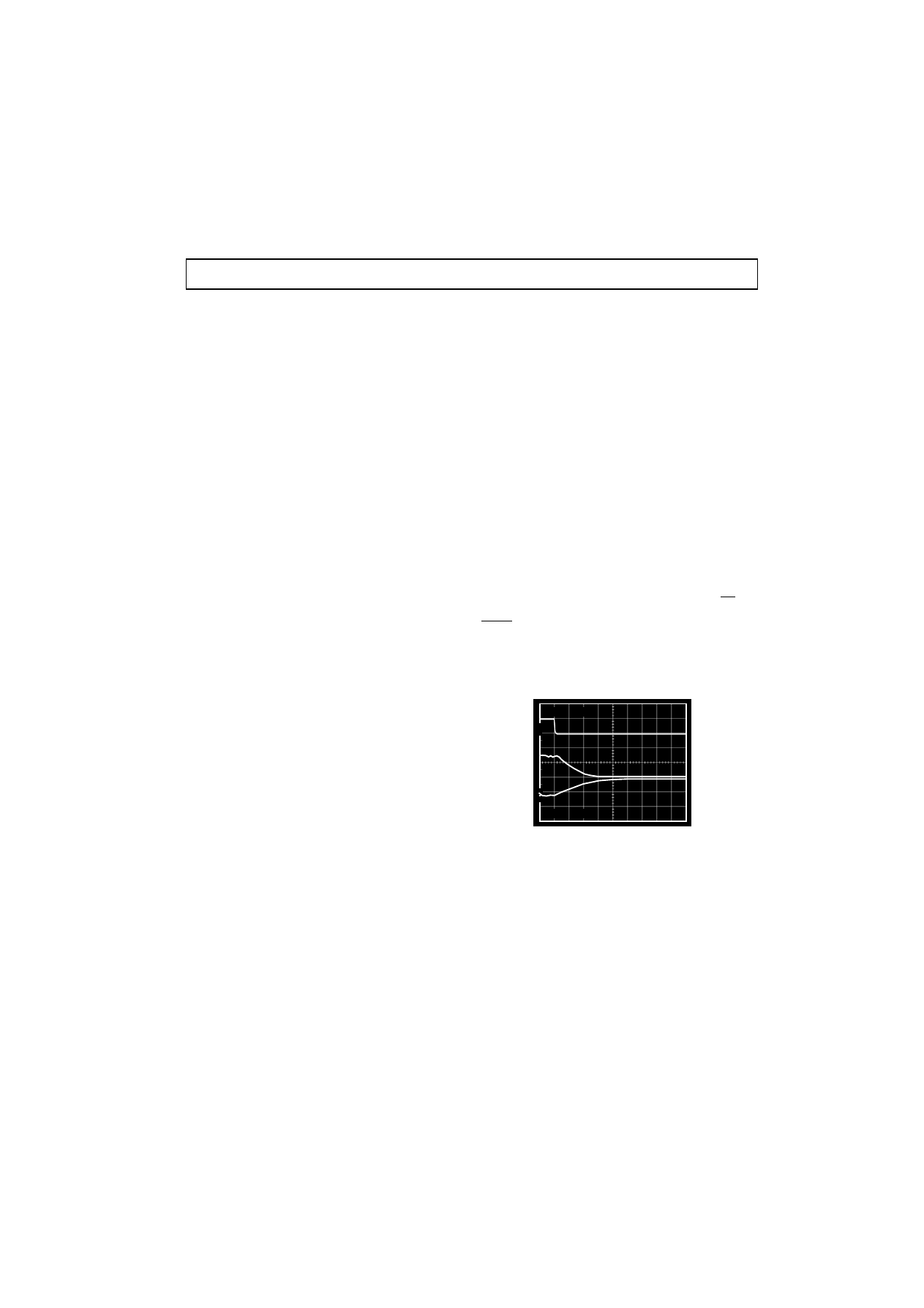
Figure 5. Shutdown Test Circuit
t
DT
+ 5V
TRANSMITTER
OUTPUT
SHDN
INPUT
– 5V
V+
0V
3V
V–
Figure 6. Transmitter Shutdown Disable Timing
NC = NO CONNECT
NC
C1+
V
CC
C2+
C2–
V–
R1
OUT
T1
IN
V+
C1–
GND
T2
OUT
T2
IN
R2
IN
R2
OUT
R1
IN
T1
OUT
1
2
18
17
5
6
7
14
13
12
3
4
16
15
8
11
9
10
TOP VIEW
(Not to Scale)
ADM222
SHDN
V
IN
V
OUT
50pF
3k
Ω
SHDN
*
INTERNAL 400k
Ω
PULL-UP RESISTOR
ON EACH TTL/MOS INPUT
**
INTERNAL 5k
Ω
PULL-DOWN RESISTOR
ON EACH RS-232 INPUT
V
CC
+5V TO +10V
VOLTAGE DOUBLER
+5V TO –10V
VOLTAGE INVERTER
C1+
C1–
V+
V–
C2+
C2–
T1
ADM222
T2
R1
R2
C1
0.1µF
C2
0.1µF
C3
0.1µF
GND
TTL/CMOS
OUTPUTS
R1
OUT
R2
OUT
T1
OUT
T2
OUT
R1
IN
R2
IN
T1
IN
T2
IN
TTL/CMOS
INPUTS
*
RS-232
OUTPUTS
RS-232
INPUTS
**
2
4
6
5
12
11
13
10
3
7
15
8
14
9
C4
0.1µF
+5V INPUT
C5
0.1µF
6.3V
17
16
18
SHDN
ADM222/ADM232A/ADM242
REV. 0
–5–
Figure 9. ADM232A DIP/SOIC Pin Configuration
Figure 11. ADM242 DIP/SOIC Pin Configuration
Figure 12. ADM242 Typical Operating Circuit
Figure 10. ADM232A Typical Operating Circuit
T2
OUT
C1+
SHDN
V
CC
C2+
C2–
V–
R1
OUT
T1
IN
V+
C1–
GND
T2
IN
R2
IN
R2
OUT
R1
IN
T1
OUT
1
2
18
17
5
6
7
14
13
12
3
4
16
15
8
11
9
10
TOP VIEW
(Not to Scale)
ADM242
EN
C1+
V+
V
CC
GND
C2–
V–
T2
OUT
R1
OUT
T1
IN
T2
IN
C1–
C2+
T1
OUT
R1
IN
R2
IN
R2
OUT
1
2
16
15
5
6
7
12
11
10
3
4
14
13
8
9
TOP VIEW
(Not to Scale)
ADM232A
V
CC
+5V TO +10V
VOLTAGE DOUBLER
+5V TO –10V
VOLTAGE INVERTER
C1+
C1–
V+
V–
C2+
C2–
T1
ADM242
T2
R1
R2
C1
0.1µF
C2
0.1µF
C3
0.1µF
GND
R1
OUT
R2
OUT
T1
OUT
T2
OUT
R1
IN
R2
IN
T1
IN
T2
IN
TTL/CMOS
INPUTS
*
RS-232
OUTPUTS
RS-232
INPUTS
**
2
4
6
5
12
11
13
10
3
7
15
14
9
C4
0.1µF
+5V INPUT
C5
0.1µF
6.3V
16
*
INTERNAL 400k
Ω
PULL-UP RESISTOR
ON EACH TTL/MOS INPUT
**
INTERNAL 5k
Ω
PULL-DOWN RESISTOR
ON EACH RS-232 INPUT
18
SHDN
17
EN
1
8
TTL/CMOS
OUTPUTS
*
TTL/CMOS
OUTPUTS
V
CC
+5V TO +10V
VOLTAGE DOUBLER
+5V TO –10V
VOLTAGE INVERTER
C1+
C1–
V+
V–
C2+
C2–
T1
ADM232A
T2
R1
R2
C1
0.1µF
C2
0.1µF
C3
0.1µF
GND
R1
OUT
R2
OUT
T1
OUT
T2
OUT
R1
IN
R2
IN
T1
IN
T2
IN
TTL/CMOS
INPUTS
*
RS-232
OUTPUTS
RS-232
INPUTS
**
1
3
5
4
11
10
12
9
2
6
14
7
13
8
C4
0.1µF
+5V INPUT
C5
0.1µF
6.3V
15
*
INTERNAL 400k
Ω
PULL-UP RESISTOR
ON EACH TTL/MOS INPUT
**
INTERNAL 5k
Ω
PULL-DOWN RESISTOR
ON EACH RS-232 INPUT
REV. 0
–6–
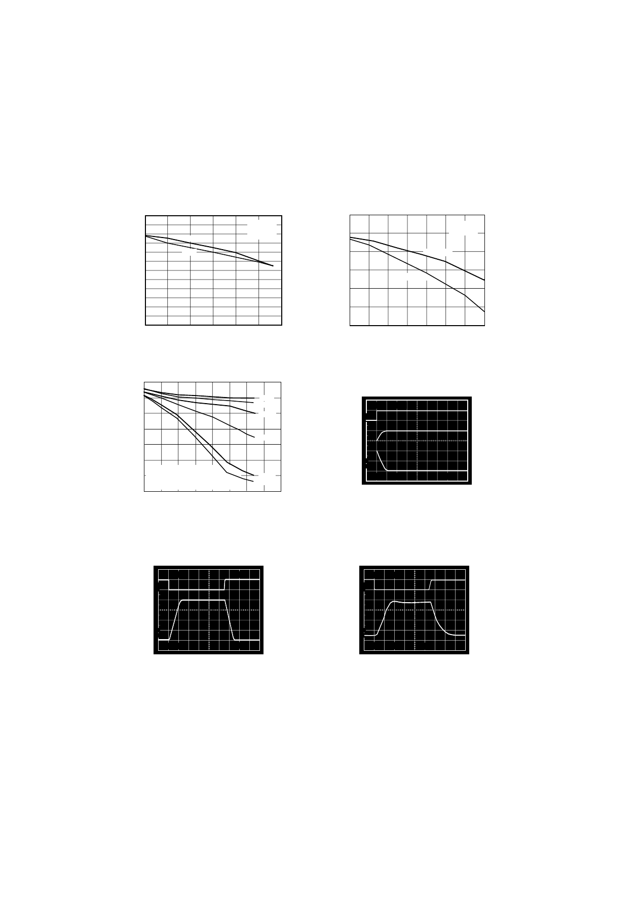
ADM222/ADM232A/ADM242–Typical Performance Characteristics
Figure 16. Transmitter Output Voltage vs. Current
Figure 13. Charge Pump V+, V– vs. Current
Figure 14. Transmitter Baud Rate vs. Load Capacitance
Figure 17. Charge Pump V+, V– Exiting Shutdown
Figure 18. Transmitter Fully Loaded Slew Rate
Figure 15. Transmitter Unloaded Slew Rate
9
2
4000
5
3
4
0
8
6
7
3000
2000
1000
20kB
60kB
120kB
200kB
400kB
500kB
LOAD CAPACITANCE – pF
TRANSMITTER OUTPUT VOLTAGE – V
V
CC
= +5V
T
A
= +25°C
TX1 = +5V; TX2 = 0V – 5V SQUARE WAVE
BOTH TX OUTPUTS LOADED WITH 3k//CL
12
0
15
2
0
6
4
8
10
10
5
V
CC
= ±5V
T
A
= +25°C
V+
I+, (
|
I–
|
) – mA
V+, (
|
V–
|
) – V
AA
AA
|
V–
|
12
0
14
2
0
6
4
8
10
10
6
I
OUT
– mA
T
OUT
– V
4
2
8
12
V
CC
= ±5V
T
A
= +25°C
T
OUT
HIGH
AAA
|
T
OUT
LOW
|
10
90
100
0%
1µs
2.4V
A2
5V
5V
10
90
100
0%
0.010V
100µs
A4
5V
5V
10
90
100
0%
–0.6 V
1 µs
5V
A1
5V
ADM222/ADM232A/ADM242
REV. 0
–7–
GENERAL INFORMATION
The ADM222/ADM232A/ADM242 are high speed RS-232
drivers/receivers requiring a single digital +5 V supply. The RS-
232 standard requires transmitters that will deliver
±
5 V
minimum on the transmission channel and receivers that can
accept signal levels down to
±
3 V. The parts achieve this by
integrating step up voltage converters and level shifting trans-
mitters and receivers onto the same chip. CMOS technology is
used to keep the power dissipation to an absolute minimum.
All devices contains an internal charge pump voltage doubler
and a voltage inverter that generates
±
10 V from the +5 V
input. Four external 0.1
µ
F capacitors are required for the
internal charge pump voltage converter.
The ADM222/ADM232A/ADM242 is a modification, enhance-
ment and improvement to the AD230-AD241 family and
derivatives thereof. It is essentially plug-in compatible and does
not have materially different applications.
CIRCUIT DESCRIPTION
The internal circuitry consists of four main sections. These are:
A Charge Pump Voltage Converter
TTL/CMOS to RS-232 Transmitters
RS-232 to TTL/CMOS Receivers
Enable and Shutdown Functions.
Charge Pump DC-DC Voltage Converter
The Charge Pump Voltage converter consists of an oscillator
and a switching matrix. The converter generates a
±
10 V supply
from the input 5 V level. This is done in two stages using a
switched capacitor technique. The 5 V input supply is doubled
to 10 V using capacitor C1 as the charge storage element. The
–10 V level is also generated from the input 5 V supply using C1
and C2 as the storage elements.
Capacitors C3 and C4 are used to reduce the output ripple.
Their values are not critical and can be reduced if higher levels
of ripple are acceptable. The charge pump capacitors C1 and
C2 may also be reduced at the expense of higher output
impedance on the V+ and V– supplies.
The V+ and V– supplies may also be used to power external
circuitry if the current requirements are small. Please refer to
the typical performance characteristics which shows the V+, V–
output voltage vs. current.
In the shutdown mode the charge pump is disabled and V+
decays to V
CC
while V– decays to 0 V.
Transmitter (Driver) Section
The Drivers convert TTL/CMOS input levels into RS-232
output levels. With V
CC
= +5 V and driving a typical RS-232
load, the output voltage swing is
±
9 V. Even under worst case
conditions the drivers are guaranteed to meet the
±
5 V RS-232
minimum requirement.
The input threshold levels are both TTL and CMOS compat-
ible with the switching threshold set at V
CC
/4. With a nominal
V
CC
= 5 V the switching threshold is 1.25 V typical. Unused
inputs may be left unconnected, as an internal 400 k
Ω
pull- up
resistor pulls them high forcing the outputs into a low state.
As required by the RS-232 standard, the slew rate is limited to
less than 30 V/
µ
s without the need for an external slew limiting
capacitor, and the output impedance in the power-off state is
greater than 300
Ω
.
Receiver Section
The receivers are inverting level shifters which accept RS-232
input levels (
±
3 V to
±
15 V) and translate them into 5 V TTL/
CMOS levels. The inputs have internal 5 k
Ω
pull-down resistors
to ground and are also protected against overvoltages of up to
±
30 V. The guaranteed switching thresholds are 0.8 V mini-
mum and 2.4 V maximum which are well within the
±
3 V RS-
232 requirement. The low level threshold is deliberately positive
as it ensures that an unconnected input will be interpreted as a
low level.
The receivers have Schmitt trigger input with a hysteresis level
of 0.5 V. This ensures error free-reception for both noisy inputs
and for inputs with slow transition times
Enable and Shutdown Functions
On the ADM222, both receivers are fully disabled during
shutdown.
On the ADM242, both receivers continue to operate normally.
This function is useful for monitoring activity so that when it
occurs, the device can be taken out of the shutdown mode.
The ADM242 also contains a receiver enable function (EN)
which can be used to fully disable the receivers, independent of
SHDN
.
APPLICATIONS INFORMATION
A selection of typical operating circuits is shown in Figures 13
to 19.
Figure 19. Transmitter Output Disable Timing
10
90
100
0%
5V
A1
5µS
2.0V
5V
ADM222/ADM232A/ADM242
REV. 0
–8–
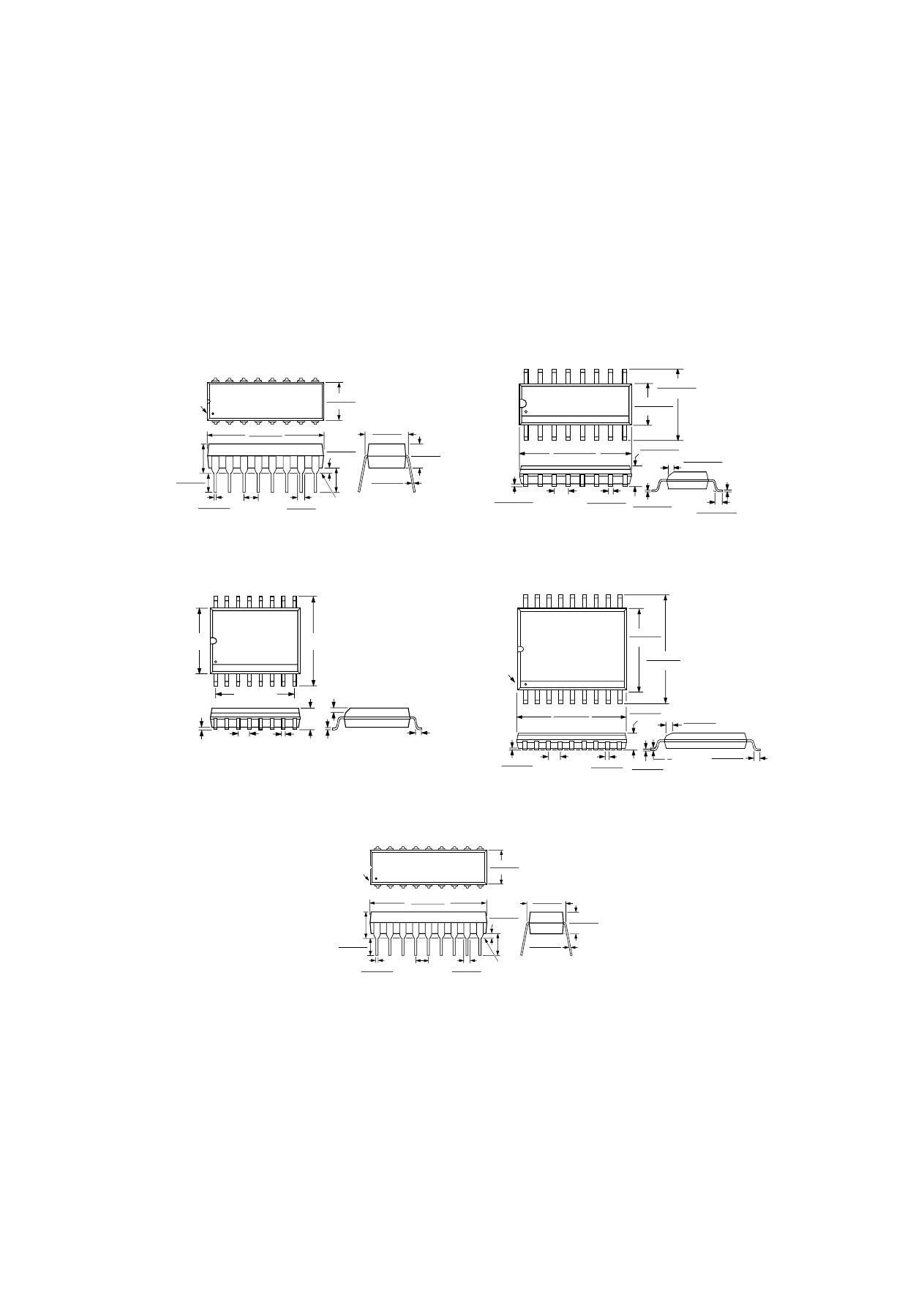
PRINTED IN U.S.A.
C1877–7.5–1/94
16-Pin Plastic DIP
(N-16)
16-Lead Wide SOIC
(R-16W)
18-Lead Wide SOIC
(R-18W)
16-Lead Narrow SOIC
(R-16N)
0.325 (8.25)
0.300 (7.62)
0.015 (0.381)
0.008 (0.204)
0.195 (4.95)
0.115 (2.93)
PIN 1
0.280 (7.11)
0.240 (6.10)
9
16
1
8
0.210
(5.33)
0.200 (5.05)
0.125 (3.18)
0.022 (0.558)
0.014 (0.356)
0.100
(2.54)
BSC
SEATING
PLANE
0.060 (1.52)
0.015 (0.38)
0.150
(3.81)
0.070 (1.77)
0.045 (1.15)
0.840 (21.33)
0.745 (18.93)
0.0688 (1.75)
0.0532 (1.35)
0.0192 (0.49)
0.0138 (0.35)
0.0500 (1.27)
BSC
8
9
16
1
0.0098 (0.25)
0.0040 (0.10)
0.3937 (10.00)
0.3859 (9.80)
0.2440 (6.20)
0.2284 (5.80)
0.1574 (4.00)
0.1497 (3.80)
0.0099 (0.25)
0.0075 (0.19)
0.0500 (1.27)
0.0160 (0.41)
0
°
– 8
°
0.0196 (0.50)
0.0099 (0.25)
0.019 (0.49)
0.05 (1.27)
REF
0.104
(2.65)
0.012
(0.3)
0.413 (10.50)
0.419
(10.65)
0.042
(1.07)
0.013
(0.32)
0.030
(0.75)
0.299
(7.60)
1
8
9
16
0.1043 (2.65)
0.0926 (2.35)
PIN 1
0.2992 (7.60)
0.2914 (7.40)
0.4193 (10.65)
0.3937 (10.00)
1
18
10
9
0.4625 (11.75)
0.4469 (11.35)
0.0192 (0.49)
0.0138 (0.35)
0.0500
(1.27)
BSC
0.0118 (0.30)
0.0040 (0.10)
0.0125 (0.32)
0.0091 (0.23)
0.0500 (1.27)
0.0157 (0.40)
8
°
0
°
0.0291 (0.74)
0.0098 (0.25)
x 45
°
18-Pin Plastic DIP
(N-18)
0.325 (8.25)
0.300 (7.62)
0.015 (0.381)
0.008 (0.204)
0.195 (4.95)
0.115 (2.93)
PIN 1
0.280 (7.11)
0.240 (6.10)
18
1
9
10
0.210
(5.33)
MAX
0.160 (4.06)
0.115 (2.93)
0.022 (0.558)
0.014 (0.356)
0.100
(2.54)
BSC
0.070 (1.77)
0.045 (1.15)
SEATING
PLANE
0.060 (1.52)
0.015 (0.38)
0.130
(3.30)
MIN
0.925 (23.49)
0.845 (21.47)
OUTLINE DIMENSIONS
Dimensions shown in inches and (mm).

ADM222/ADM232A/ADM242
REV. 0
–9–
ORDERING GUIDE
Model
Temperature Range
Package Option*
ADM222AN
–40
°
C to +85
°
C
N-18
ADM222AR
–40
°
C to +85
°
C
R-18W
ADM232AAN
–40
°
C to +85
°
C
N-16
ADM232AARN
–40
°
C to +85
°
C
R-16N
ADM232AARW
–40
°
C to +85
°
C
R-16W
ADM242AN
–40
°
C to +85
°
C
N-18
ADM242AR
–40
°
C to +85
°
C
R-18W
*For outline information see Package Information section.
Wyszukiwarka
Podobne podstrony:
Abolicja podatkowa id 50334 Nieznany (2)
4 LIDER MENEDZER id 37733 Nieznany (2)
katechezy MB id 233498 Nieznany
metro sciaga id 296943 Nieznany
perf id 354744 Nieznany
interbase id 92028 Nieznany
Mbaku id 289860 Nieznany
Probiotyki antybiotyki id 66316 Nieznany
miedziowanie cz 2 id 113259 Nieznany
LTC1729 id 273494 Nieznany
D11B7AOver0400 id 130434 Nieznany
analiza ryzyka bio id 61320 Nieznany
pedagogika ogolna id 353595 Nieznany
Misc3 id 302777 Nieznany
cw med 5 id 122239 Nieznany
D20031152Lj id 130579 Nieznany
mechanika 3 id 290735 Nieznany
więcej podobnych podstron