REV. 0
Information furnished by Analog Devices is believed to be accurate and
reliable. However, no responsibility is assumed by Analog Devices for its
use, nor for any infringements of patents or other rights of third parties
which may result from its use. No license is granted by implication or
otherwise under any patent or patent rights of Analog Devices.
a
Low Cost, 250 mA Output
Single-Supply Amplifiers
AD8531/AD8532/AD8534
© Analog Devices, Inc., 1996
One Technology Way, P.O. Box 9106, Norwood, MA 02062-9106, U.S.A.
Tel: 617/329-4700
Fax: 617/326-8703
GENERAL DESCRIPTION
The AD8531, AD8532 and AD8534 are single, dual and quad
rail-to-rail input and output single-supply amplifiers featuring
250 mA output drive current. This high output current makes
these amplifiers excellent for driving either resistive or capacitive
loads. AC performance is very good with 3 MHz bandwidth,
5 V/
µ
s slew rate and low distortion. All are guaranteed to oper-
ate from a +3 volt single supply as well as a +5 volt supply.
The very low input bias currents enable the AD853x to be used
for integrators and diode amplification and other applications
requiring low input bias current. Supply current is only 750
µ
A
per amplifier at 5 volts, allowing low current applications to con-
trol high current loads.
Applications include audio amplification for computers, sound
ports, sound cards and set-top boxes. AD853x family is very
stable and capable of driving heavy capacitive loads, such as
those found in LCDs.
The ability to swing rail-to-rail at the inputs and outputs enables
designers to buffer CMOS DACs, ASICs or other wide output
swing devices in single-supply systems.
The AD8531, AD8532 and AD8534 are specified over the ex-
tended industrial (–40
°
C to +85
°
C) temperature range. The
AD8531 is available in SO-8 and SOT23-5 packages. The
AD8532 is available in 8-pin plastic DIPs, SO-8 and 8-lead
TSSOP surface mount packages. The AD8534 is available in
14-pin plastic DIPs, narrow SO-14 are 14-lead TSSOP surface
mount packages. All TSSOP and SOT versions are available in
tape and reel only.
FEATURES
Single-Supply Operation: 2.7 Volts to 6 Volts
High Output Current:
6250 mA
Low Supply Current: 750
mA/Amplifier
Wide Bandwidth: 3 MHz
Slew Rate: 5 V/
ms
No Phase Reversal
Low Input Currents
Unity Gain Stable
APPLICATIONS
Multimedia Audio
LCD Driver
ASIC Input or Output Amplifier
Headphone Driver
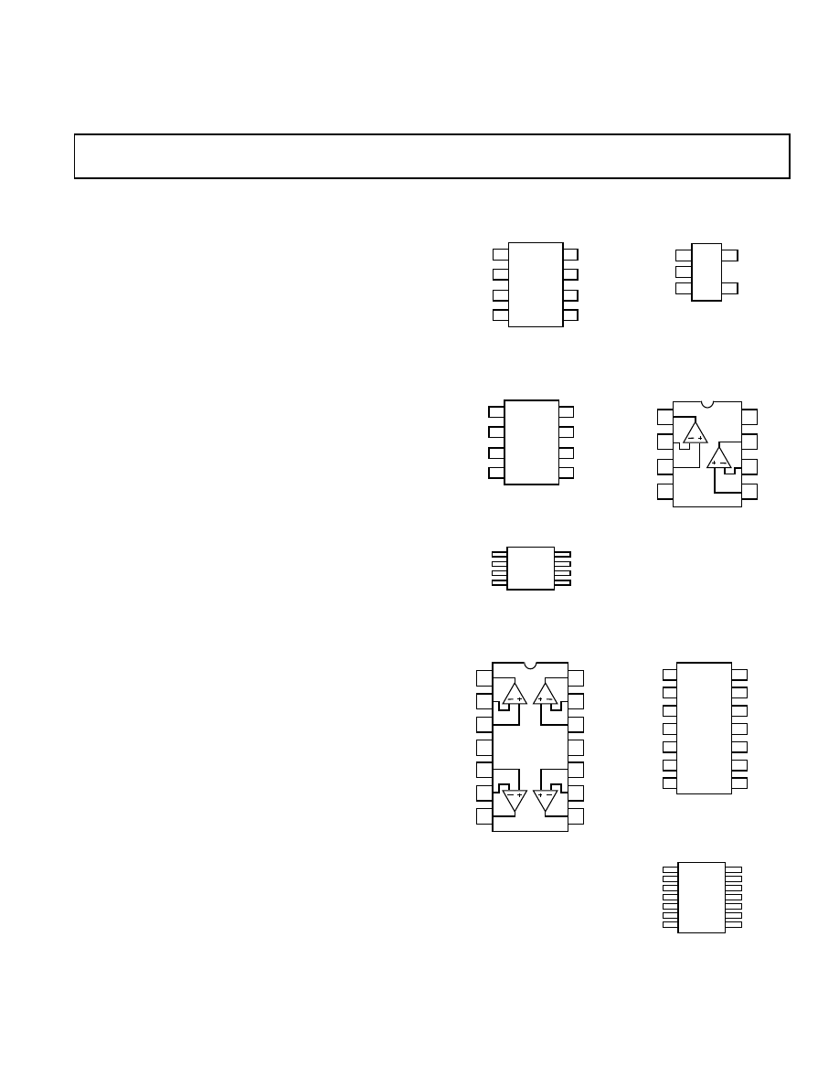
PIN CONFIGURATIONS
5-Lead SOT
(RT Suffix)
AD8531
OUT A
V–
+IN A
–IN A
V+
1
2
3
4
5
8-Lead SO
(R Suffix)
AD8532
OUT A
–IN A
+IN A
V–
V+
OUT B
+IN B
1
2
3
4
8
7
6
5
(Not to Scale)
–IN B
8-Lead Epoxy DIP
(N Suffix)
AD8532
1
2
3
4
8
7
6
5
OUT A
–IN A
+IN A
V–
+IN B
–IN B
OUT B
V+
(Not to
Scale)
8-Lead SO
(R Suffix)
AD8531
NULL
–IN A
+IN A
V–
V+
OUT A
NULL
NC
1
2
3
4
8
7
6
5
(Not to Scale)
8-Lead TSSOP
(RU Suffix)
–IN A
+IN A
V–
OUT B
–IN B
+IN B
V+
1
4
5
8
AD8532
OUT A
14-Lead Epoxy DIP
(N Suffix)
AD8534
1
2
3
4
14
13
12
11
OUT A
–IN A
+IN A
V+
V–
+IN D
–IN D
OUT D
5
6
7
10
9
8
+IN B
–IN B
OUT B
OUT C
–IN C
+IN C
(Not to Scale)
14-Lead
Narrow-Body SO
(R Suffix)
AD8534
OUT A
–IN A
+IN A
V+
–IN D
+IN D
V–
OUT D
1
2
3
4
14
13
12
11
(Not to Scale)
+IN B
–IN B
OUT B
–IN C
OUT C
+IN C
5
6
7
10
9
8
AD8534
(Not to Scale)
14-Lead TSSOP
(RU Suffix)
AD8532
OUT A
–IN A
+IN A
V+
–IN D
+IN D
V–
OUT D
1
14
+IN B
–IN B
OUT B
–IN C
OUT C
+IN C
7
8
AD8534
1
14
7
8

REV. 0
–2–
AD8531/AD8532/AD8534–SPECIFICATIONS
ELECTRICAL CHARACTERISTICS
Parameter
Symbol
Conditions
Min
Typ
Max
Units
INPUT CHARACTERISTICS
Offset Voltage
V
OS
25
mV
–40
°
C
≤
T
A
≤
+85
°
C
30
mV
Input Bias Current
I
B
5
50
pA
–40
°
C
≤
T
A
≤
+85
°
C
60
pA
Input Offset Current
I
OS
1
25
pA
–40
°
C
≤
T
A
≤
+85
°
C
30
pA
Input Voltage Range
0
3
V
Common-Mode Rejection Ratio
CMRR
V
CM
= 0 V to 3 V
38
45
dB
Large Signal Voltage Gain
A
VO
R
L
= 2 k
Ω
, V
O
= 0.5 V to 2.5 V
25
V/mV
Offset Voltage Drift
∆
V
OS
/
∆
T
20
µ
V/
°
C
Bias Current Drift
∆
I
B
/
∆
T
50
fA/
°
C
Offset Current Drift
∆
I
OS
/
∆
T
20
fA/
°
C
OUTPUT CHARACTERISTICS
Output Voltage High
V
OH
I
L
= 10 mA
2.85
2.92
V
–40
°
C
≤
T
A
≤
+85
°
C
2.8
V
Output Voltage Low
V
OL
I
L
= 10 mA
60
100
mV
–40
°
C
≤
T
A
≤
+85
°
C
125
mV
Output Current
I
OUT
±
250
mA
Closed-Loop Output Impedance
Z
OUT
f = 1 MHz, A
V
= 1
60
Ω
POWER SUPPLY
Power Supply Rejection Ratio
PSRR
V
S
= 3 V to 6 V
45
55
dB
Supply Current/Amplifier
I
SY
V
O
= 0 V
1
mA
–40
°
C
≤
T
A
≤
+85
°
C
1.25
mA
DYNAMIC PERFORMANCE
Slew Rate
SR
R
L
= 2 k
Ω
3.5
V/
µ
s
Settling Time
t
S
To 0.01%
1.4
µ
s
Gain Bandwidth Product
GBP
2.2
MHz
Phase Margin
φ
o
70
Degrees
Channel Separation
CS
f = 1 kHz, R
L
= 2 k
Ω
65
dB
NOISE PERFORMANCE
Voltage Noise Density
e
n
f = 1 kHz
45
nV/
√
Hz
Voltage Noise Density
e
n
f = 10 kHz
30
nV/
√
Hz
Current Noise Density
i
n
f = 1 kHz
0.05
pA/
√
Hz
Specifications subject to change without notice.
(@ V
S
= +3.0 V, V
CM
= 1.5 V, T
A
= +25
8C unless otherwise noted)

ELECTRICAL CHARACTERISTICS
Parameter
Symbol
Conditions
Min
Typ
Max
Units
INPUT CHARACTERISTICS
Offset Voltage
V
OS
25
mV
–40
°
C
≤
T
A
≤
+85
°
C
30
mV
Input Bias Current
I
B
5
50
pA
–40
°
C
≤
T
A
≤
+85
°
C
60
pA
Input Offset Current
I
OS
1
25
pA
–40
°
C
≤
T
A
≤
+85
°
C
30
pA
Input Voltage Range
0
5
V
Common-Mode Rejection Ratio
CMRR
V
CM
= 0 V to 5 V
38
47
dB
Large Signal Voltage Gain
A
VO
R
L
= 2 k
Ω
, V
O
= 0.5 V to 4.5 V
15
80
V/mV
Offset Voltage Drift
∆
V
OS
/
∆
T
–40
°
C
≤
T
A
≤
+85
°
C
20
µ
V/
°
C
Bias Current Drift
∆
I
B
/
∆
T
50
fA/
°
C
Offset Current Drift
∆
I
OS
/
∆
T
20
fA/
°
C
OUTPUT CHARACTERISTICS
Output Voltage High
V
OH
I
L
= 10 mA
4.9
4.94
V
–40
°
C
≤
T
A
≤
+85
°
C
4.85
V
Output Voltage Low
V
OL
I
L
= 10 mA
50
100
mV
–40
°
C
≤
T
A
≤
+85
°
C
125
mV
Output Current
I
OUT
±
250
mA
Closed-Loop Output Impedance
Z
OUT
f = 1 MHz, A
V
= 1
40
Ω
POWER SUPPLY
Power Supply Rejection Ratio
PSRR
V
S
= 3 V to 6 V
45
55
dB
Supply Current/Amplifier
I
SY
V
O
= 0 V
1.4
1.25
mA
–40
°
C
≤
T
A
≤
+85
°
C
1.75
mA
DYNAMIC PERFORMANCE
Slew Rate
SR
R
L
= 2 k
Ω
5
V/
µ
s
Full-Power Bandwidth
BW
p
1% Distortion
350
kHz
Settling Time
t
S
To 0.01%
1.6
µ
s
Gain Bandwidth Product
GBP
3
MHz
Phase Margin
φ
o
70
Degrees
Channel Separation
CS
f = 1 kHz, R
L
= 2 k
Ω
65
dB
NOISE PERFORMANCE
Voltage Noise Density
e
n
f = 1 kHz
45
nV/
√
Hz
Voltage Noise Density
e
n
f = 10 kHz
30
nV/
√
Hz
Current Noise Density
i
n
f = 1 kHz
0.05
pA/
√
Hz
Specifications subject to change without notice.
AD8531/AD8532/AD8534
REV. 0
–3–
(@ V
S
= +5.0 V, V
CM
= 2.5 V, T
A
= +25
8C unless otherwise noted)
AD8531/AD8532/AD8534
REV. 0
–4–
ABSOLUTE MAXIMUM RATINGS
Supply Voltage (V
S
) . . . . . . . . . . . . . . . . . . . . . . . . . . . . . +7 V
Input Voltage . . . . . . . . . . . . . . . . . . . . . . . . . . . . . GND to V
S
Differential Input Voltage
1
. . . . . . . . . . . . . . . . . . . . . . .
±
6 V
Storage Temperature Range
N, R, RT, RU Package . . . . . . . . . . . . . . . –65
°
C to +150
°
C
Operating Temperature Range
AD8531/AD8532/AD8534 . . . . . . . . . . . . . –40
°
C to +85
°
C
Junction Temperature Range
N, R, RT, RU Package . . . . . . . . . . . . . . . –65
°
C to +150
°
C
Lead Temperature Range (Soldering, 60 sec) . . . . . . +300
°
C
PACKAGE INFORMATION
Package Type
u
JA
2
u
JC
Units
5-Lead SOT-23 (RT)
230
°
C/W
8-Pin SOIC (R)
158
43
°
C/W
8-Pin TSSOP (RU)
240
43
°
C/W
14-Pin Plastic DIP (N)
83
39
°
C/W
14-Pin SOIC (R)
120
36
°
C/W
14-Pin TSSOP (RU)
240
43
°
C/W
NOTES
1
For supplies less than +6 volts, the differential input voltage is equal to
±
V
S
.
2
θ
JA
is specified for the worst case conditions, i.e.,
θ
JA
is specified for device in socket
for P-DIP packages;
θ
JA
is specified for device soldered onto a circuit board for
surface mount packages.
ORDERING GUIDE
Temperature
Package
Package
Model
Range
Description
Option
AD8531AR
–40
°
C to +85
°
C
8-Pin SOIC
SO-8
AD8531ART
1
–40
°
C to +85
°
C
5-Lead SOT-23
RT-5
AD8532AR
–40
°
C to +85
°
C
8-Pin SOIC
SO-8
AD8532AN
–40
°
C to +85
°
C
8-Pin Plastic DIP
N-8
AD8532ARU
2
–40
°
C to +85
°
C
8-Pin TSSOP
RU-8
AD8534AR
–40
°
C to +85
°
C
14-Pin SOIC
SO-14
AD8534AN
–40
°
C to +85
°
C
14-Pin Plastic DIP
N-14
AD8534ARU
2
–40
°
C to +85
°
C
14-Pin TSSOP
RU-14
NOTES
1
Available in 2,500 piece reels only.
2
Available in 2,500 piece reels only.
WARNING!
ESD SENSITIVE DEVICE
CAUTION
ESD (electrostatic discharge) sensitive device. Electrostatic charges as high as 4000 V readily
accumulate on the human body and test equipment and can discharge without detection.
Although the AD8531/AD8532/AD8534 feature proprietary ESD protection circuitry, permanent
damage may occur on devices subjected to high energy electrostatic discharges. Therefore, prope r
ESD precautions are recommended to avoid performance degradation or loss of functionality.
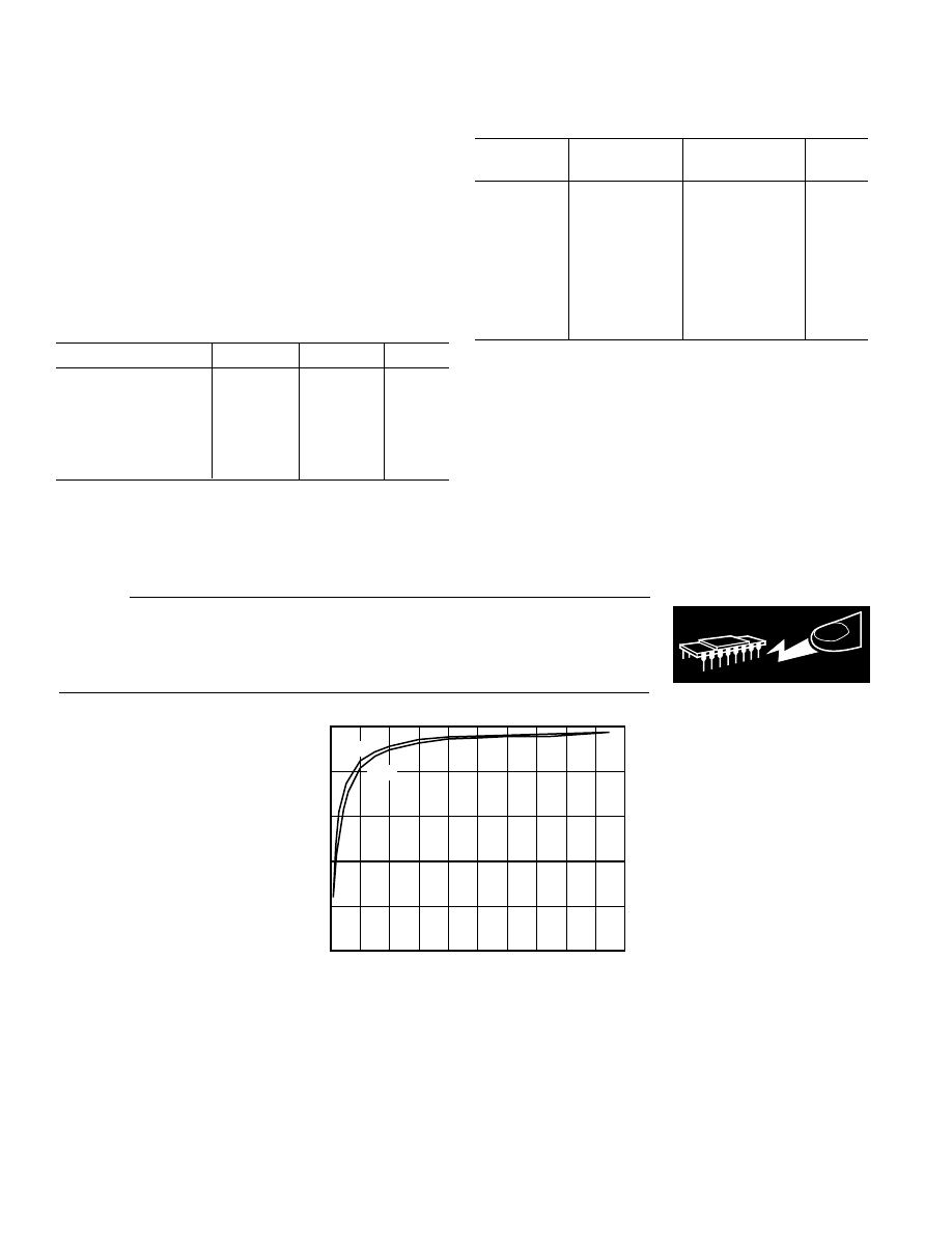
2.5
2
1.5
1
0.5
0
0
20
40
60
80
100
120
140
160
180
200
R
LOAD
–
Ω
±
V
OUT
+V
OH
–V
OL
Figure 1. Output Voltage vs. Load. V
S
=
±
2.5 V, R
L
Is Connected to GND (0 V)
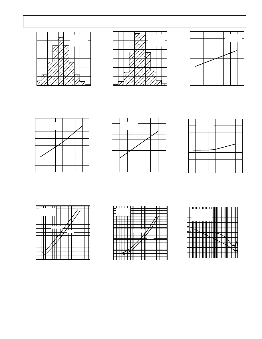
INPUT OFFSET VOLTAGE – mV
QUANTITY – Amplifiers
300
–12 –10 –8
–6
–4
–2
0
2
4
500
400
200
100
V
S
= +2.7V
V
CM
= +1.35V
T
A
= +25
8
C
Figure 2. Input Offset Voltage
Distribution
TEMPERATURE –
8
C
INPUT BIAS CURRENT – pA
5
–35 –15
5
25
45
65
85
8
7
4
2
V
S
= +5V, +3V
V
CM
= V
S
/2
6
3
Figure 5. Input Bias Current vs.
Temperature
LOAD CURRENT – mA
∆
OUTPUT VOLTAGE – mV
1000
100
0.1
0.01
0.1
1000
1
10
10
1
100
V
S
= +2.7V
T
A
= +25
8
C
SOURCE
SINK
Figure 8. Output Voltage to Supply
Rail vs. Load Current
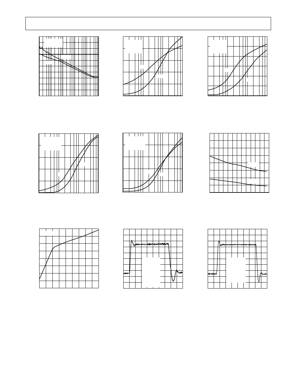
Typical Performance Characteristics–AD8531/AD8532/AD8534
REV. 0
–5–
INPUT OFFSET VOLTAGE – mV
QUANTITY – Amplifiers
300
–12 –10 –8
–6
–4
–2
0
2
4
500
400
200
100
V
S
= +5V
V
CM
= +2.5V
T
A
= +25
8
C
Figure 3. Input Offset Voltage
Distribution
COMMON-MODE VOLTAGE – Volts
INPUT BIAS CURRENT – pA
5
0
1
2
3
4
5
8
7
4
2
V
S
= +5V
T
A
= +25
8
C
6
3
1
Figure 6. Input Bias Current vs.
Common-Mode Voltage
LOAD CURRENT – mA
∆
OUTPUT VOLTAGE – mV
10000
100
0.01
0.01
0.1
1000
1
10
100
10
1000
1
V
S
= +5V
T
A
= +25
8
C
SOURCE
SINK
Figure 9. Output Voltage to Supply
Rail vs. Load Current
TEMPERATURE –
8
C
INPUT OFFSET VOLTAGE – mV
–5
–35 –15
5
25
45
65
85
–2
–3
–6
–8
V
S
= +5V
V
CM
= +2.5V
–4
–7
Figure 4. Input Offset Voltage
vs. Temperature
TEMPERATURE –
8
C
INPUT OFFSET CURRENT – pA
3
–35
–15
5
25
45
65
2
0
V
S
= +5V, +3V
V
CM
= V
S
/2
4
1
–1
85
–2
5
6
Figure 7. Input Offset Current vs.
Temperature
80
60
40
20
0
GAIN – dB
V
S
= +2.7V
R
L
= NO LOAD
T
A
= +25
8
C
45
90
135
180
PHASE SHIFT – Degrees
FREQUENCY – Hz
1k
10k
100k
1M
10M
100M
Figure 10. Open-Loop Gain & Phase
vs. Frequency
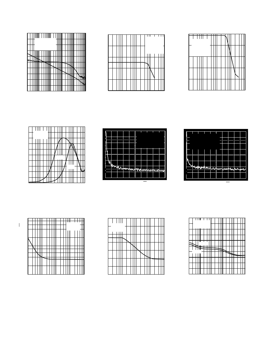
AD8531/AD8532/AD8534–Typical Performance Characteristics
REV. 0
–6–
80
60
40
20
0
GAIN – dB
V
S
= +5V
R
L
= NO LOAD
T
A
= +25
8
C
45
90
135
180
PHASE SHIFT – Degrees
FREQUENCY – Hz
1k
10k
100k
1M
10M
100M
Figure 11. Open-Loop Gain & Phase
vs. Frequency
FREQUENCY – Hz
IMPEDANCE –
Ω
1k
10k
100M
100k
1M
10M
160
140
120
100
80
60
40
20
V
S
= +5V
T
A
= +25
8
C
A
V
= 10
A
V
= 1
180
200
0
Figure 14. Closed-Loop Output
Impedance vs. Frequency
FREQUENCY – Hz
CURRENT NOISE DENSITY – pA/
√
Hz
1
0.1
0.01
10
100
100k
1k
10k
V
S
= +5V
T
A
= +25
8
C
Figure 17. Current Noise Density
vs. Frequency
FREQUENCY – Hz
OUTPUT SWING – Volts p-p
5
4
0
1k
10k
10M
100k
1M
3
2
1
V
S
= +2.7V
T
A
= +25
8
C
R
L
= 2k
Ω
V
IN
= 2.5V p-p
Figure 12. Closed-Loop Output
Voltage Swing vs. Frequency
100
90
10
0%
V
S
= +5V
A
V
= 1000
T
A
= +25
8
C
FREQUENCY = 1kHz
100
µ
V/div
MARKER 41
µ
V/
√
Hz
Figure 15. Voltage Noise Density
vs. Frequency
FREQUENCY – Hz
COMMON-MODE REJECTION – dB
90
80
20
1k
10k
10M
100k
1M
60
50
30
V
S
= +5V
T
A
= +25
8
C
70
40
Figure 18. Common-Mode Rejec-
tion vs. Frequency
FREQUENCY – Hz
OUTPUT SWING – Volts p-p
5
4
0
1k
10k
10M
100k
1M
3
2
1
V
S
= +5V
T
A
= +25
8
C
R
L
= 2k
Ω
V
IN
= 4.9V p-p
Figure 13. Closed-Loop Output
Voltage Swing vs. Frequency
100
90
10
0%
V
S
= +5V
A
V
= 1000
T
A
= +25
8
C
FREQUENCY = 10kHz
MARKER 25.9
µ
V/
√
Hz
200
µ
V/div
Figure 16. Voltage Noise Density
vs. Frequency
80
60
40
20
0
POWER SUPPLY REJECTION – dB
100
120
140
–60
–40
–20
FREQUENCY – Hz
1k
10k
100k
1M
10M
100
V
S
= +2.7V
T
A
= +25
8
C
PSRR–
PSRR+
Figure 19. Power Supply Rejection
vs. Frequency
AD8531/AD8532/AD8534
REV. 0
–7–
80
60
40
20
0
POWER SUPPLY REJECTION – dB
FREQUENCY – Hz
1k
10k
100k
1M
10M
100
100
120
140
–60
–40
–20
V
S
= +5V
T
A
= +25
8
C
PSRR–
PSRR+
Figure 20. Power Supply Rejection
vs. Frequency
CAPACITANCE – pF
SMALL SIGNAL OVERSHOOT – %
50
40
0
10
100
10000
1000
30
20
10
V
S
= +5V
T
A
= +25
8
C
R
L
= 600
Ω
–OS
+OS
Figure 23. Small Signal Overshoot
vs. Load Capacitance
SUPPLY VOLTAGE –
6
Volts
SUPPLY CURRENT/AMPLIFIER – mA
0.80
0.30
0.00
0.75 1.00
1.50
2.00
2.50
3.00
0.70
0.40
0.20
0.10
0.60
0.50
T
A
= +25
8
C
Figure 26. Supply Current per
Amplifier vs. Supply Voltage
CAPACITANCE – pF
SMALL SIGNAL OVERSHOOT – %
50
40
0
10
100
10000
1000
30
20
10
V
S
= +2.7V
T
A
= +25
8
C
R
L
= 2k
Ω
–OS
+OS
Figure 21. Small Signal Overshoot
vs. Load Capacitance
CAPACITANCE – pF
SMALL SIGNAL OVERSHOOT – %
50
40
0
10
100
10000
1000
30
20
10
V
S
= +2.7V
T
A
= +25
8
C
R
L
= 600
Ω
–OS
+OS
Figure 24. Small Signal Overshoot
vs. Load Capacitance
500 ns/DIV
20mV/DIV
V
S
=
6
1.35V
V
IN
=
6
50mV
A
V
= 1
R
L
= 2k
Ω
C
L
= 300pF
T
A
= +25
8
C
0V
Figure 27. Small Signal Transient
Response
CAPACITANCE – pF
SMALL SIGNAL OVERSHOOT – %
50
40
0
10
100
10000
1000
30
20
10
V
S
= +5V
T
A
= +25
8
C
R
L
= 2k
Ω
60
–OS
+OS
Figure 22. Small Signal Overshoot
vs. Load Capacitance
TEMPERATURE –
8
C
SUPPLY CURRENT/AMPLIFIER – mA
0.9
0.65
0.5
–40
–20
0
20
40
60
80
0.85
0.7
0.6
0.55
0.8
0.75
V
S
= 5V
V
S
= 3V
Figure 25. Supply Current per
Amplifier vs. Temperature
500 ns/DIV
20mV/DIV
V
S
=
6
2.5V
V
IN
=
6
50mV
A
V
= 1
R
L
= 2k
Ω
C
L
= 300pF
T
A
= +25
8
C
0V
Figure 28. Small Signal Transient
Response
AD8531/AD8532/AD8534
REV. 0
–8–
APPLICATIONS
THEORY OF OPERATION
The AD8531/AD8532/AD8534 is an all-CMOS, high output
current drive, rail-to-rail input/output operational amplifier.
This is the latest entry in Analog Devices’ expanding family of
single-supply devices for the multimedia and telecom market-
places. Its high output current drive and stability with heavy ca-
pacitive loads makes the AD8531/AD8532/AD8534 an excellent
choice as a drive amplifier for LCD panels.
Figure 32 illustrates a simplified equivalent circuit for the AD8531/
AD8532/AD8534. Like many rail-to-rail input amplifier configura-
tions, it is comprised of a two differential pairs, one n-channel
(M1–M2) and one p-channel (M3–M4). These differential pairs
are biased by 50
µ
A current sources, each with a compliance
limit of approximately 0.5 V from either supply voltage rail. The
differential input voltage is then converted into a pair of differen-
tial output currents. These differential output currents are then
combined together in a compound folded-cascode second gain
stage (M5–M9). The outputs of the second gain stage at M8
and M9 provide the gate voltage drive to the rail-to-rail, output
stage. Additional signal current recombination for the output
stage is achieved through the use of transistors M11–M14.
In order to achieve rail-to-rail output swings, the AD8531/AD8532/
AD8534 design employs a complementary common-source output
stage (M15–M16). However, the output voltage swing is directly
dependent on the load current, as the difference between the out-
put voltage and the supply is determined by the AD8531/AD8532/
AD8534’s output transistors on-channel resistance (see Figures 8
and 9). The output stage also exhibits voltage gain by virtue of
the use of common-source amplifiers; and as a result the volt-
age gain of the output stage (thus, the open-loop gain of the
device) exhibits a strong dependence to the total load resistance
at the output of the AD8531/AD8532/AD8534.
50
µ
A
100
µ
A
100
µ
A
20
µ
A
V
B2
M5
M8
M12
M15
M16
M11
OUT
M3
M4
M2
M1
IN–
IN+
V
B3
M6
M7
M10
20
µ
A
M13
50
µ
A
V+
V–
M9
M14
Figure 32. AD8531/AD8532/AD8534 Simplified Equivalent
Circuit
Short-Circuit Protection
As a result of the design of the output stage for maximum load
current capability, the AD8531/AD8532/AD8534 does not have
any internal short-circuit protection circuitry. Direct connection of
the AD8531/AD8532/AD8534’s output to the positive supply
in single-supply applications will destroy the device. In those
applications where some protection is needed, but not at the ex-
pense of reduced output voltage headroom, a low value resistor
in series with the output, as shown in Figure 33, can be used.
The resistor, connected within the feedback loop of the ampli-
fier, will have very little effect on the performance of the ampli-
fier other than limiting the maximum available output voltage
swing. For single +5 V supply applications, resistors less than
20
Ω
are not recommended.
+5V
R
X
20
Ω
V
OUT
V
IN
AD8532
Figure 33. Output Short-Circuit Protection
10
0%
500ns
500mV
100
90
V
S
=
6
1.35V
A
V
= 1
R
L
= 2k
Ω
T
A
= +25
8
C
Figure 30. Large Signal Transient
Response
10
0%
500ns
500mV
100
90
V
S
=
6
2.5V
A
V
= 1
R
L
= 2k
Ω
T
A
= +25
8
C
Figure 29. Large Signal Tran-
sient Response
10
0%
10
m
s
1V
100
90
1V
Figure 31. No Phase Reversal
AD8531/AD8532/AD8534
REV. 0
–9–
Power Dissipation
Although the AD8531/AD8532/AD8534 is capable of providing
load currents to 250 mA, the usable output load current drive
capability will be limited to the maximum power dissipation al-
lowed by the device package used. In any application, the abso-
lute maximum junction temperature for the AD8531/AD8532/
AD8534 is 150
°
C, and should never be exceeded for the device
could suffer premature failure. Accurately measuring power
dissipation of an integrated circuit is not always a straightfor-
ward exercise, so Figure 34 has been provided as a design aid
for either setting a safe output current drive level or in selecting
a heat sink for the three package options available on the
AD8531/AD8532/AD8534.
TEMPERATURE –
8
C
1.5
1
0
0
100
25
POWER DISSIPATION – Watts
50
75
0.5
85
T
J
MAX = 150
8
C
FREE AIR
NO HEAT SINK
PDIP
θ
JA
= 103
8
C/W
SOIC
θ
JA
= 158
8
C/W
TSSOP
θ
JA
= 240
8
C/W
Figure 34. Maximum Power Dissipation vs. Ambient
Temperature
These thermal resistance curves were determined using the
AD8531/AD8532/AD8534 thermal resistance data for each
package and a maximum junction temperature of 150
°
C. The fol-
lowing formula can be used to calculate the internal junction tem-
perature of the AD8531/AD8532/AD8534 for any application:
T
J
= P
DISS
×
θ
JA
+ T
A
where
T
J
= junction temperature;
P
DISS
= power dissipation;
θ
JA
= package thermal resistance,
junction-to-case; and
T
A
= Ambient temperature of the circuit.
To calculate the power dissipated by the AD8531/AD8532/
AD8534, the following equation can be used:
P
DISS
= I
LOAD
×
(V
S
–V
OUT
)
where
I
LOAD
= is output load current;
V
S
= is supply voltage; and
V
OUT
= is output voltage.
The quantity within the parentheses is the maximum voltage
developed across either output transistor. As an additional de-
sign aid in calculating available load current from the AD8531/
AD8532/AD8534, Figure 1 illustrates the AD8531/AD8532/
AD8534 output voltage as a function of load resistance.
Power Calculations for Varying or Unknown Loads
Often, calculating power dissipated by an integrated circuit to
determine if the device is being operated in a safe range is not as
simple as it might seem. In many cases power cannot be mea-
sured directly. This may be the result of irregular output wave-
forms or varying loads. So indirect methods of measuring
power are required.
Here are two methods to calculate power dissipated by an inte-
grated circuit. The first can be done by measuring the package
temperature and the board temperature. The other method is
to directly measure the circuit’s supply current.
Calculating Power by Measuring Ambient and Case
Temperature
Given the two equations for calculating junction temperature:
T
J
= T
A
+ P
θ
JA
where T
J
is junction temperature, and T
A
is ambient tempera-
ture.
θ
JA
is the junction to ambient thermal resistance.
T
J
= T
C
+ P
θ
JC
where T
C
is case temperature and
θ
JA
and
θ
JC
are given in the
data sheet.
The two equations can be solved for P (power):
T
A
+ P
θ
JA
= T
C
+ P
θ
JC
P = (T
A
– T
C
)/ (
θ
JC
–
θ
JA
)
Once power has been determined it is necessary to go back and
calculate the junction temperature to assure that it has not
been exceeded.
The temperature measurements should be directly on the
package and on a spot on the board that is near the package
but definitely not touching it. Measuring the package could be
difficult. A very small bimetallic junction glued to the package
could be used or it could be done using an infrared sensing
device if the spot size is small enough.
Calculating Power by Measuring Supply Current
Power can be calculated directly knowing the supply voltage
and current. However, supply current may have a dc compo-
nent with a pulse into a capacitive load. This could make rms
current very difficult to calculate.
This can be overcome by lifting the supply pin and inserting an
rms current meter into the circuit. For this to work you must
be sure all of the current is being delivered by the supply pin
that you are measuring. This is usually a good method in a
single supply system. However, if the system uses dual sup-
plies, both supplies may need to be monitored.
Input Overvoltage Protection
As with any semiconductor device, whenever the condition ex-
ists for the input to exceed either supply voltage, the device’s
input overvoltage characteristic must be considered. When an
overvoltage occurs, the amplifier could be damaged depending
on the magnitude of the applied voltage and the magnitude of
the fault current. Although not shown here, when the input
voltage exceeds either supply by more than 0.6 V, pn-junctions
internal to the AD8531/AD8532/AD8534 energize allowing
current to flow from the input to the supplies. As illustrated in
the simplified equivalent input circuit (Figure 32), the AD8531/
AD8532/AD8534 does not have any internal current limiting
resistors, so fault currents can quickly rise to damaging levels.
This input current is not inherently damaging to the device as
long as it is limited to 5 mA or less. For the AD8531/AD8532/
AD8534, once the input voltage exceeds the supply by more
than 0.6 V the input current quickly exceeds 5 mA. If this
AD8531/AD8532/AD8534
REV. 0
–10–
condition continues to exist, an external series resistor should
be added. The size of the resistor is calculated by dividing the
maximum overvoltage by 5 mA. For example, if the input volt-
age could reach 10 V, the external resistor should be (10 V/5
mA) = 2 k
Ω
. This resistance should be placed in series with
either or both inputs if they are exposed to an overvoltage con-
dition. For more information on general overvoltage character-
istics of amplifiers refer to the 1993 Seminar Applications Guide,
available from the Analog Devices Literature Center.
Output Phase Reversal
Some operational amplifiers designed for single-supply opera-
tion exhibit an output voltage phase reversal when their inputs
are driven beyond their useful common-mode range. The
AD8531/AD8532/AD8534 is free from reasonable input voltage
range restrictions provided that the input voltages no greater
than the supply voltage rails are applied. Although the device’s
output will not change phase, large currents can flow through
internal junctions to the supply rails, as was pointed out in the
previous section. Without limit, these fault currents can easily
destroy the amplifier. Therefore, the technique recommended
in the input overvoltage protection section should be applied in
those applications where the possibility of input voltages ex-
ceeding the supply voltages exists.
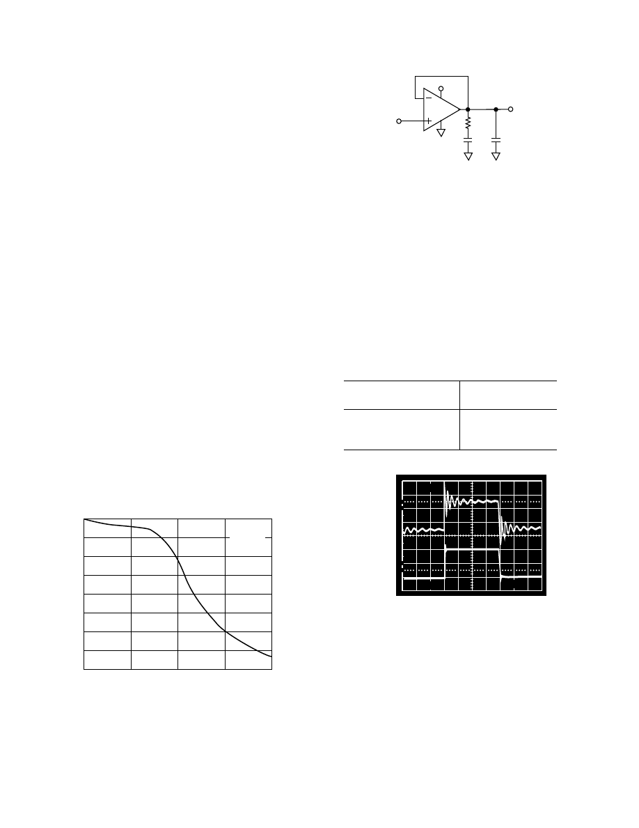
Capacitive Load Drive
The AD8531/AD8532/AD8534 exhibits excellent capacitive
load driving capabilities. It can drive up to 10 nF directly as
shown in Figures 21 through 24. However, even though the
device is stable, a capacitive load does not come without a pen-
alty in bandwidth. As shown in Figure 35, the bandwidth is re-
duced to under 1 MHz for loads greater than 10 nF. A “snubber”
network on the output won’t increase the bandwidth, but it
does significantly reduce the amount of overshoot for a given
capacitive load. A snubber consists of a series R-C network
(R
S
, C
S
), as shown in Figure 36, connected from the output of
the device to ground. This network operates in parallel with the
load capacitor, C
L
, to provide phase lag compensation. The actual
value of the resistor and capacitor is best determined empirically.
CAPACITIVE LOAD – nF
4
3.5
0
0.01
100
0.1
BANDWIDTH – MHz
1
10
2
1.5
1
0.5
3
2.5
V
S
=
6
2.5V
R
L
= 1k
Ω
T
A
= +25
8
C
Figure 35. Unity-Gain Bandwidth vs. Capacitive Load
+5V
R
S
5
Ω
V
OUT
V
IN
100mV p-p
AD8532
C
L
47nF
C
S
1µF
Figure 36. Snubber Network Compensates for Capacitive
Loads
The first step is to determine the value of the resistor, R
S
. A
good starting value is 100
Ω
. This value is reduced until the
small-signal transient response is optimized. Next, C
S
is deter-
mined—10
µ
F is a good starting point. This value is reduced to
the smallest value for acceptable performance (typically, 1
µ
F).
For the case of a 47 nF load capacitor on the AD8531/AD8532/
AD8534, the optimal snubber network is a 5
Ω
in series with
1
µ
F. The benefit is immediately apparent as seen in the scope
photo in Figure 37. The top trace was taken with a 47 nF load
and the bottom trace with the 5
Ω
—1
µ
F snubber network in
place. The amount of overshoot and ringing is dramatically re-
duced. Table I below illustrates a few sample snubber networks
for large load capacitors:
Table I. Snubber Networks for Large Capacitive Loads
Load Capacitance
Snubber Network
(C
L
)
(R
S
, C
S
)
0.47 nF
300
Ω
, 0.1
µ
F
4.7 nF
30
Ω
, 1
µ
F
47 nF
5
Ω
, 1
µ
F
10
0%
10
m
s
50mV
100
90
50mV
47nF LOAD
ONLY
SNUBBER
IN CIRCUIT
Figure 37. Overshoot and Ringing Is Reduced by Adding
a Snubber Network in Parallel with the 47 nF Load
AD8531/AD8532/AD8534
REV. 0
–11–
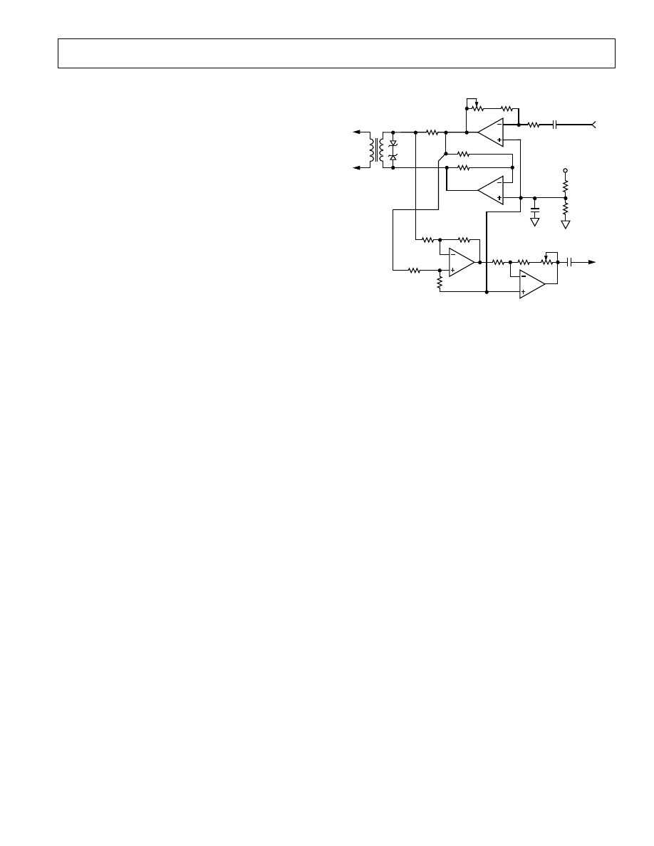
A High Output Current, Buffered Reference/Regulator
Many applications require stable voltage outputs relatively close
in potential to an unregulated input source. This “low drop-
out” type of reference/regulator is readily implemented with a
rail-to-rail output op amp, and is particularly useful when using
a higher current device such as the AD8531/AD8532/AD8534.
A typical example is the 3.3 V or 4.5 V reference voltage devel-
oped from a 5 V system source. Generating these voltages re-
quires a three terminal reference, such as the REF196 (3.3 V) or
the REF194 (4.5 V), both which feature low power, with sourc-
ing outputs of 30 mA or less. Figure 38 shows how such a ref-
erence can be outfitted with an AD8531/AD8532/AD8534
buffer for higher currents and/or voltage levels, plus sink and
source load capability.
C2
0.1µF
R2
10k
Ω
1%
V
OUT1
=
3.3V @ 100mA
R5
0.2
Ω
C5
100µF/16V
TANTALUM
R1
10k
Ω
1%
C1
0.1µF
+V
S
+5V
V
OUT2
=
3.3V
C4
1µF
6
2
3
4
V
OUT
COMMON
C3
0.1µF
V
C
ON/OFF
CONTROL
INPUT CMOS HI
(OR OPEN) = ON
LO = OFF
V
S
COMMON
R3
(SeeText)
R4
3.3k
Ω
U2
AD8531
U1
REF196
Figure 38. A High Output Current Reference/Regulator
The low dropout performance of this circuit is provided by
stage U2, an AD8531 connected as a follower/buffer for the basic
reference voltage produced by U1. The low voltage saturation
characteristic of the AD8531/AD8532/AD8534 allows up to
100 mA of load current in the illustrated use, as a 5 V to 3.3 V
converter with good dc accuracy. In fact, the dc output voltage
change for a 100 mA load current delta measured less than
1 mV. This corresponds to an equivalent output impedance of
< 0.01
Ω
. In this application, the stable 3.3 V from U1 is ap-
plied to U2 through a noise filter, R1–C1. U2 replicates the U1
voltage within a few millivolts, but at a higher current output at
V
OUT1
, with the ability to both sink and source output current(s)
—unlike most IC references. R2 and C2 in the feedback path of
U2 provide additional noise filtering.
Transient performance of the reference/regulator for a 100 mA
step change in load current is also quite good and is determined
largely by the R5–C5 output network. With values as shown,
the transient is about 20 mV peak and settles to within 2 mV in
less than 10
µ
s for either polarity. Although there exists room
for optimizing the transient response, any changes to the R5–C5
network should be verified by experiment to preclude the possi-
bility of excessive ringing with some capacitor types.
To scale V
OUT2
to another (higher) output level, the optional
resistor R3 (shown dotted) is added causing the new V
OUT1
to
become:
V
OUT 1
=
V
OUT 2
×
1
+
R2
R3
The circuit can be used either as shown as a 5 V to 3.3 V
reference/regulator, or it can also be used with ON/OFF con-
trol. By driving Pin 3 of U1 with a logic control signal as noted,
the output is switched ON/OFF. Note that when ON/OFF con-
trol is used, resistor R4 must be used with U1, to speed ON-
OFF switching.
A Single-Supply, Balanced Line Driver
The circuit in Figure 39 is a unique line driver circuit topology
used in professional audio applications and has been modified
for the automotive and multimedia audio applications. On a
single +5 V supply, the line driver exhibits less than 0.7% dis-
tortion into a 600
Ω
load from 20 Hz to 15 kHz (not shown)
with an input signal level of 4 V p-p. In fact, the output drive
capability of the AD8531/AD8532/AD8534 maintains this level
for loads as small as 32
Ω
. For input signals less than 1 V p-p,
the THD is less than 0.1%, regardless of load. The design is a
transformerless, balanced transmission system where output
common-mode rejection of noise is of paramount importance.
Like the transformer-based system, either output can be shorted
to ground for unbalanced line driver applications without
changing the circuit gain of 1. Other circuit gains can be set ac-
cording to the equation in the diagram. This allows the design
to be easily configured for noninverting, inverting, or differential
operation.
R
L
600
Ω
C1
22µF
A2
7
6
5
3
1
2
A1
+5V
R1
10k
Ω
R2
10k
Ω
R11
10k
Ω
R7
10k
Ω
6
7
5
A1
+12V
+5V
R8
100k
Ω
R9
100k
Ω
C2
1µF
R12
10k
Ω
R14
50
Ω
A2
1
2
3
R3
10k
Ω
R6
10k
Ω
R13
10k
Ω
C3
47µF
V
O1
V
O2
C4
47µF
A1, A2 = 1/2 AD8532
GAIN =
R3
R2
SET: R7, R10, R11 = R2
SET: R6, R12, R13 = R3
V
IN
R10
10k
Ω
R5
50
Ω
Figure 39. A Single-Supply, Balanced Line Driver for
Multimedia and Automotive Applications
AD8531/AD8532/AD8534
REV. 0
–12–
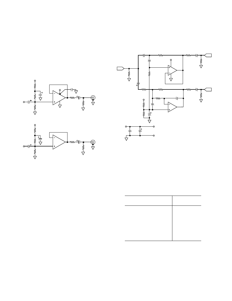
A Single-Supply Headphone Amplifier
Because of its speed and large output drive, the AD8531/AD8532/
AD8534 makes for an excellent headphone driver, as illustrated
in Figure 40. Its low supply operation and rail-to-rail inputs
and outputs give a maximum signal swing on a single +5 V sup-
ply. To insure maximum signal swing available to drive the
headphone, the amplifier inputs are biased to V+/2, which is in
this case 2.5 V. The 100 k
Ω
resistor to the positive supply is
equally split into two 50 k
Ω
resistors with their common point
bypassed by 10
µ
F to prevent power supply noise from contami-
nating the audio signal.
1/2
AD8532
16
Ω
50k
Ω
270µF
LEFT
HEADPHONE
10µF
50k
Ω
50k
Ω
100k
Ω
10µF
LEFT
INPUT
+V + 5V
1/2
AD8532
16
Ω
50k
Ω
270µF
RIGHT
HEADPHONE
10µF
50k
Ω
50k
Ω
100k
Ω
10µF
RIGHT
INPUT
+V
+V + 5V
1µF/0.1µF
Figure 40. A Single-Supply, Stereo Headphone Driver
The audio signal is then ac-coupled to each input through a
10
µ
F capacitor. A large value is needed to ensure that the
20 Hz audio information is not blocked. If the input already has
the proper dc bias, then the ac coupling and biasing resistors are
not required. A 270
µ
F capacitor is used at the output to couple
the amplifier to the headphone. This value is much larger than
that used for the input because of the low impedance of the
headphones, which can range from 32
Ω
to 600
Ω
. An addi-
tional 16
Ω
resistor is used in series with the output capacitor to
protect the op amp’s output stage by limiting capacitor dis-
charge current. When driving a 48
Ω
load, the circuit exhibits
less than 0.3% THD+N at output drive levels of 4 V p-p.
A Single-Supply, Two-Way Loudspeaker Crossover Network
Active filters are useful in loudspeaker crossover networks for
reasons of small size, relative freedom from parasitic effects, and
the ease of controlling low/high channel drive, plus the controlled
driver damping provided by a dedicated amplifier. Both Sallen-
Key (SK) and multiple-feedback (MFB) filter architectures are
useful in implementing active crossover networks. The circuit
shown in Figure 41 is a single-supply, two-way active crossover
which combines the advantages of both filter topologies. This
active crossover exhibits less than 0.4% THD+N at output lev-
els of 1.4 V rms using general purpose unity-gain HP/LP stages.
In this two-way example, the LO signal is a dc-500 Hz LP
woofer output, and the HI signal is the HP (>500 Hz)
tweeter output. U1B forms an LP section at 500 Hz, while
U1A provides a HP section, covering frequencies
≥
500 Hz.
V
IN
3
2
1
U1A
AD8532
+V
S
4
R1
31.6k
Ω
C1
0.01µF
C2
0.01µF
R2
31.6k
Ω
R5
31.6k
Ω
R6
31.6k
Ω
R4
49.9
Ω
HI
LO
500Hz
AND UP
DC –
500Hz
6
5
7
C3
0.01µF
U1B
AD8532
C4
0.02µF
R7
15.8k
Ω
R3
49.9
Ω
270µF
270µF
100k
Ω
+V
S
10µF
100k
Ω
100k
Ω
C
IN
10µF
R
IN
100k
Ω
0.1µF
100µF/25V
+V
S
TO U1
+5V
COM
+
100k
Ω
+
Figure 41. A Single-Supply, Two-Way Active Crossover
The crossover example frequency of 500 Hz can be shifted
lower or higher by frequency scaling of either resistors or ca-
pacitors. In configuring the circuit for other frequencies,
complementary LP/HP action must be maintained between
sections, and component values within the sections must be in
the same ratio. Table II provides a design aid to adaptation,
with suggested standard component values for other frequencies.
Table II. RC Component Selection for Various
Crossover Frequencies
Crossover
R1/C1 (U1A)
1
Frequency (Hz)
R5/C3 (U1B)
2
100
160 k
Ω
/0.01
µ
F
200
80.6 k
Ω
/0.01
µ
F
319
49.9 k
Ω
/0.01
µ
F
500
31.6 k
Ω
/0.01
µ
F
1 k
16 k
Ω
/0.01
µ
F
2 k
8.06 k
Ω
/0.01
µ
F
5 k
3.16 k
Ω
/0.01
µ
F
10 k
1.6 k
Ω
/0.01
µ
F
NOTES
Applicable for filter
α
= 2.
1
For Sallen-Key stage U1A: R1 = R2, and C1 = C2, etc.
2
For Multiple Feedback stage U1B: R6 = R5, R7 = R5/2, and
C4 = 2C3.
For additional information on the active filters and active cross-
over networks, please consult the data sheet for the OP279, a
dual rail-to-rail high-output current operational amplifier.
AD8531/AD8532/AD8534
REV. 0
–13–
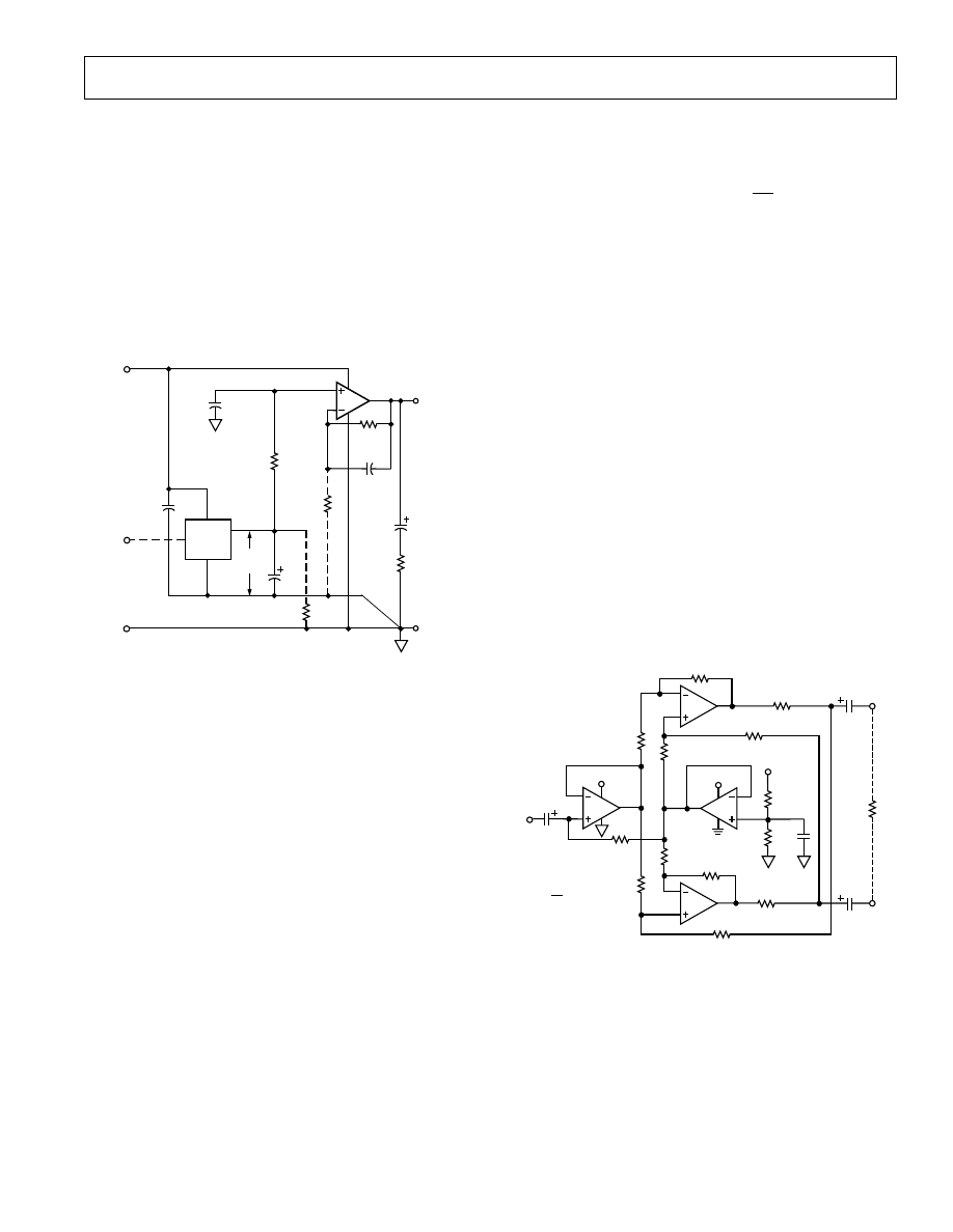
Direct Access Arrangement for Telephone Line Interface
Figure 42 illustrates a +5 V only transmit/receive telephone line
interface for 600
Ω
transmission systems. It allow full duplex
transmission of signals on a transformer coupled 600
Ω
line in a
differential manner. Amplifier A1 provides gain which can be
adjusted to meet the modem output drive requirements. Both
A1 and A2 are configured so as to apply the largest possible sig-
nal on a single supply to the transformer. Because of the
AD8531/AD8532/AD8534’s high output current drive and low
dropout voltage, the largest signal available on a single +5 V
supply is approximately 4.5 V p-p into a 600
Ω
transmission sys-
tem. Amplifier A3 is configured as a difference amplifier for
two reasons: (1) It prevents the transmit signal from interfering
with the receive signal, and (2) it extracts the receive signal from
the transmission line for amplification by A4. A4’s gain can be
adjusted in the same manner as A1’s to meet the modem’s input
signal requirements. Standard resistor values permit the use of
SIP (Single In-line Package) format resistor arrays. Couple this
with the AD8531/AD8532/AD8534’s 8-pin SOIC or TSSOP
footprint and this circuit offers a compact, cost-sensitive solution.
6.2V
6.2V
TRANSMIT
TXA
RECEIVE
RXA
C1
0.1µF
R1
10k
Ω
R2
9.09k
Ω
2k
Ω
P1
TX GAIN
ADJUST
A1
A2
A3
A4
A1, A2 = 1/2 AD8532
A3, A4 = 1/2 AD8532
R3
360
Ω
1:1
T1
TO TELEPHONE
LINE
1
2
3
7
6
5
2
3
1
6
5
7
10µF
R7
10k
Ω
R8
10k
Ω
R5
10k
Ω
R6
10k
Ω
R9
10k
Ω
R14
14.3k
Ω
R10
10k
Ω
R11
10k
Ω
R12
10k
Ω
R13
10k
Ω
C2
0.1µF
P2
RX GAIN
ADJUST
2k
Ω
Z
O
600
Ω
+5V DC
MIDCOM
671-8005
Figure 42. A Single-Supply Direct Access Arrange-
ment for Modems

AD8531/AD8532/AD8534
REV. 0
–14–
* AD8531/AD8532/AD8534 SPICE Macro-model 3/96, Rev. A
* 5-Volt Version ARG / ADSC
*
* Copyright 1996 by Analog Devices
*
* Refer to “README.DOC” file for License Statement. Use of this model
* indicates your acceptance of the terms and provisions in the License
* Statement.
*
* Node assignments
*
noninverting input
*
|
inverting input
*
|
|
positive supply
*
|
|
|
negative supply
*
|
|
|
|
output
*
|
|
|
|
|
.SUBCKT AD8531/AD8532/AD8534_5 1
2
99
50
40
*
* INPUT STAGE
*
M1
3
2
6
50
NIX L=6U W=25U
M2
4
7
6
50
NIX L=6U W=25U
M3
8
2
5
5
PIX
L=6U W=25U
M4
9
7
5
5
PIX
L=6U W=25U
EOS
7
1
POLY(1)
25
98
5E-3 0.451
IIN1
1
98
5P
IIN2
2
98
5P
IOS
2
1
0.5P
I1
99
5
50U
I2
6
50
50U
R1
99
3
4.833K
R2
99
4
4.833K
R3
8
50
4.833K
R4
9
50
4.833K
D3
5
99
DX
D4
50
6
DX
*
* GAIN
STAGE
*
EREF
98
0
POLY(2)
99
0
50
0
0
0.5
+0.5
G1
98
21
POLY(2)
4
3
9
8
0
+145U
+145U
RG
21
98
18.078E6
CC
21
40
14P
D1
21
22
DX
D2
23
21
DX
V1
99
22
1.37
V2
23
50
1.37
*
* COMMON MODE GAIN STAGE
*
ECM
24
98
POLY(2)
1
98
2
98
0
0.5
+0.5
R5
24
25
1E6
R6
25
98
10K
C1
24
25
0.75P
*
* OUTPUT STAGE
*
ISY
99
50
450.4U
GSY
99
50
POLY(1)
99
50
-3.334E-4
6.667E-5
EP
99
39
POLY(1)
98
21
0.78925
1
EN
38
50
POLY(1)
21
98
0.78925
1
M15
40
39
99
99
POX L=1.5U
W=1500U
M16
40
38
50
50
NOX L=1.5U
W=1500U
C15
40
39
50P
C16
40
38
50P
.MODEL DX D(RS=1 CJO=0.1P)
.MODEL NIX NMOS(VTO=0.75 KP=205.5U RD=1 RS=1 RG=1 RB=1
+CGSO=4E-9
+CGDO=4E-9 CGBO=16.667E-9 CBS=2.34E-13 CBD=2.34E-13)
.MODEL NOX NMOS(VTO=0.75 KP=195U RD=.5 RS=.5 RG=1 RB=1
+CGSO=66.667E-12
+CGDO=66.667E-12 CGBO=125E-9 CBS=2.34E-13 CBD=2.34E-13)
.MODEL PIX PMOS(VTO=-0.75 KP=205.5U RD=1 RS=1 RG=1 RB=1
+CGSO=4E-9
+CGDO=4E-9 CBDO=16.667E-9 CBS=2.34E-13 CBD=2.34E-13)
.MODEL POX PMOS(VTO=-0.75 KP=195U RD=.5 RS=.5 RG=1 RB=1
+CGSO=66.667E-12
+CGDO=66.667E-12 CGBO=125E-9 CBS=2.34E-13 CBD=2.34E-13)
.ENDS
AD8531/AD8532/AD8534
REV. 0
–15–
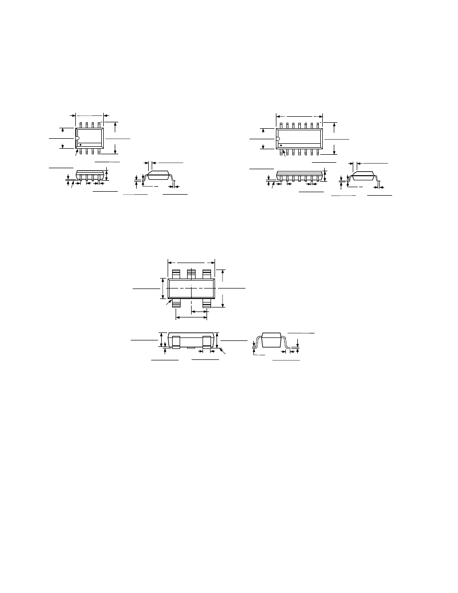
OUTLINE DIMENSIONS
Dimensions shown in inches and (mm).
8-Pin Plastic DIP
(N-8)
8
1
4
5
0.430 (10.92)
0.348 (8.84)
0.280 (7.11)
0.240 (6.10)
PIN 1
SEATING
PLANE
0.022 (0.558)
0.014 (0.356)
0.060 (1.52)
0.015 (0.38)
0.210 (5.33)
MAX
0.130
(3.30)
MIN
0.070 (1.77)
0.045 (1.15)
0.100
(2.54)
BSC
0.160 (4.06)
0.115 (2.93)
0.325 (8.25)
0.300 (7.62)
0.015 (0.381)
0.008 (0.204)
0.195 (4.95)
0.115 (2.93)
8-Pin TSSOP
(RU-8)
8
5
4
1
0.122 (3.10)
0.114 (2.90)
0.256 (6.50)
0.246 (6.25)
0.177 (4.50)
0.169 (4.30)
PIN 1
0.0256 (0.65)
BSC
SEATING
PLANE
0.006 (0.15)
0.002 (0.05)
0.0118 (0.30)
0.0075 (0.19)
0.0433
(1.10)
MAX
0.0079 (0.20)
0.0035 (0.090)
0.028 (0.70)
0.020 (0.50)
8
°
0
°
14-Pin TSSOP
(RU-14)
14
8
7
1
0.201 (5.10)
0.193 (4.90)
0.256 (6.50)
0.246 (6.25)
0.177 (4.50)
0.169 (4.30)
PIN 1
SEATING
PLANE
0.006 (0.15)
0.002 (0.05)
0.0118 (0.30)
0.0075 (0.19)
0.0256
(0.65)
BSC
0.0433
(1.10)
MAX
0.0079 (0.20)
0.0035 (0.090)
0.028 (0.70)
0.020 (0.50)
8
°
0
°
14-Pin Plastic DIP
(N-14)
14
1
7
8
0.795 (20.19)
0.725 (18.42)
0.280 (7.11)
0.240 (6.10)
PIN 1
0.325 (8.25)
0.300 (7.62)
0.015 (0.381)
0.008 (0.204)
0.195 (4.95)
0.115 (2.93)
SEATING
PLANE
0.022 (0.558)
0.014 (0.356)
0.060 (1.52)
0.015 (0.38)
0.210 (5.33)
MAX
0.130
(3.30)
MIN
0.070 (1.77)
0.045 (1.15)
0.100
(2.54)
BSC
0.160 (4.06)
0.115 (2.93)
AD8531/AD8532/AD8534
REV. 0
–16–
C2149–18–7/96
PRINTED IN U.S.A.
OUTLINE DIMENSIONS
Dimensions shown in inches and (mm).
8-Pin SOIC
(SO-8)
0.1968 (5.00)
0.1890 (4.80)
8
5
4
1
0.2440 (6.20)
0.2284 (5.80)
PIN 1
0.1574 (4.00)
0.1497 (3.80)
0.0688 (1.75)
0.0532 (1.35)
SEATING
PLANE
0.0098 (0.25)
0.0040 (0.10)
0.0192 (0.49)
0.0138 (0.35)
0.0500
(1.27)
BSC
0.0098 (0.25)
0.0075 (0.19)
0.0500 (1.27)
0.0160 (0.41)
8
°
0
°
0.0196 (0.50)
0.0099 (0.25)
x 45
°
14-Pin SOIC
(SO-14)
14
8
7
1
0.3444 (8.75)
0.3367 (8.55)
0.2440 (6.20)
0.2284 (5.80)
0.1574 (4.00)
0.1497 (3.80)
PIN 1
SEATING
PLANE
0.0098 (0.25)
0.0040 (0.10)
0.0192 (0.49)
0.0138 (0.35)
0.0688 (1.75)
0.0532 (1.35)
0.0500
(1.27)
BSC
0.0099 (0.25)
0.0075 (0.19)
0.0500 (1.27)
0.0160 (0.41)
8
°
0
°
0.0196 (0.50)
0.0099 (0.25)
x 45
°
5-Lead SOT-23
(RT-5)
0.0079 (0.200)
0.0035 (0.090)
0.0236 (0.600)
0.0039 (0.100)
10
°
0
°
0.0197 (0.500)
0.0118 (0.300)
0.0590 (0.150)
0.0000 (0.000)
0.0512 (1.300)
0.0354 (0.900)
SEATING
PLANE
0.0571 (1.450)
0.0354 (0.900)
0.1220 (3.100)
0.1063 (2.700)
PIN 1
0.0709 (1.800)
0.0590 (1.500)
0.1181 (3.000)
0.0984 (2.500)
1
2
3
4
5
0.0748 (1.900)
REF
0.0374 (0.950) REF
NOTE:
PACKAGE OUTLINE INCLUSIVE AS SOLDER PLATING.
Wyszukiwarka
Podobne podstrony:
Abolicja podatkowa id 50334 Nieznany (2)
4 LIDER MENEDZER id 37733 Nieznany (2)
katechezy MB id 233498 Nieznany
metro sciaga id 296943 Nieznany
perf id 354744 Nieznany
interbase id 92028 Nieznany
Mbaku id 289860 Nieznany
Probiotyki antybiotyki id 66316 Nieznany
miedziowanie cz 2 id 113259 Nieznany
LTC1729 id 273494 Nieznany
D11B7AOver0400 id 130434 Nieznany
analiza ryzyka bio id 61320 Nieznany
pedagogika ogolna id 353595 Nieznany
Misc3 id 302777 Nieznany
cw med 5 id 122239 Nieznany
D20031152Lj id 130579 Nieznany
mechanika 3 id 290735 Nieznany
więcej podobnych podstron