Laboratory Exercise 6
Adders, Subtractors, and Multipliers
The purpose of this exercise is to examine arithmetic circuits that add, subtract, and
multiply numbers. Each type of circuit will be implemented in two ways: first by writing VHDL
code that describes the required functionality, and second by making use of predefined
subcircuits from Altera’s library of parameterized modules (LPMs). The results produced for
various implementations will be compared, both in terms of the circuit structure and its speed
of operation.
Part I
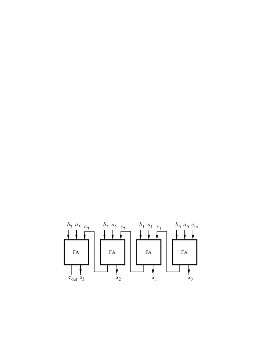
Consider again the four-bit ripple-carry adder circuit that was used in lab exercise 2; a
diagram of this circuit is reproduced in Figure 1a. You are to create an 8-bit version of the
adder and include it in the circuit shown in Figure 1b. Your circuit should be designed to
support signed numbers in 2’s-complement form, and the Overflow output should be set to 1
whenever the sum produced by the adder does not provide the correct signed value.
Perform the steps shown below.
a) Four-bit ripple-carry adder circuit
1
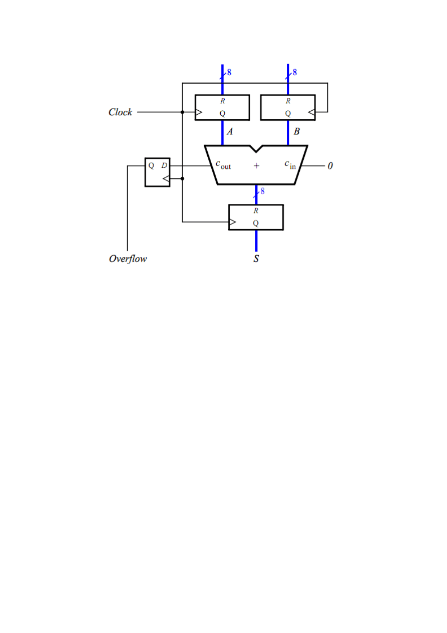
b) Eight-bit registered adder circuit
Figure 1.An 8-bit signed adder with registered inputs and outputs.
1. Make a new Quartus II project and write VHDL code that describes the circuit in Figure 1b.
Use the circuit structure in Figure 1a to describe your adder.
2. Include the required input and output ports in your project to implement the adder circuit on
the DE2-115 board.
3. Connect the inputs A and B to switches SW15−8 and SW7−0, respectively. Use KEY0
as an active-low asynchronous reset input, and use KEY1 as a manual clock input.
Display the sum outputs of the adder on the red LEDR7−0 lights and display the overflow
output on the green LEDG 8 light. The hexadecimal values of A and B should be shown on
the displays HEX7-6 and HEX5-4, and the hexadecimal value of S should appear on
HEX1-0.
4. Compile your code and use timing simulation to verify the correct operation of the circuit.
Once the simulation works properly, download the circuit onto the DE2-115 board and test
it by using different values of A and B. Be sure to check for proper functionality of the
Overflow output.
2

5. Open the Quartus II Compilation Report and examine the results reported by the Timing
Analyzer. What is the maximum operating frequency, fmax, of your circuit? What is the
longest path in the circuit in terms of delay?
Part II
Modify your circuit from Part I so that it can perform both addition and subtraction of
eight-bit numbers. Use switch SW16 to specify whether addition or subtraction should be
performed. Connect the other switches, lights, and displays as described for Part I.
1. Simulate your adder/subtractor circuit to show that it functions properly, and then
download it onto the DE2-115 board and test it by using different switch settings.
2. Open the Quartus II Compilation Report and examine the results reported by the Timing
Analyzer. What is the fmax of your circuit? What is the longest path in the circuit in terms of
delay?
Part III
Repeat Part I using the predefined adder circuit called lpm add sub, instead of your
ripple-carry adder structure from Figure 1. The lpm add sub module can be found in Altera’s
library of parameterized modules (LPMs), which is provided as part of the Quartus II system.
The procedure for using these predefined modules in Quartus II projects is described in the
tutorial Using Library Modules in VHDL Designs, which is available on the DE2-115 System
CD and in the University Program section of Altera’s web site.
1. Configure the lpm add sub module so that it performs only addition, to make the
functionality comparable to Part I. Store your configuration of the lpm add sub module in
the file lpm add8.v. After instantiating this module in your VHDL code, compile the project
and use the Quartus II Chip Editor tool to examine some of the details of the implemented
circuit. One way to examine the adder subcircuit using the Chip Editor tool is illustrated in
Figure 2. In the Quartus II Project Navigator window right-click on the part of your circuit
hierarchy that represents the lpm add8 subcircuit, and select the command Locate >
Locate in Chip Editor. This opens the Chip Editor window shown in Figure 3. The logic
elements in the Cyclone IV FPGA that are used to implement the adder are highlighted in
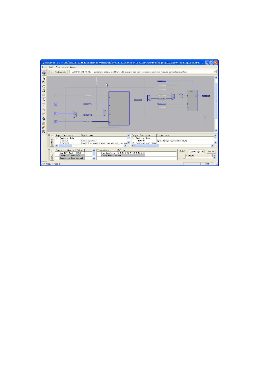
blue in the Chip Editor tool. Position your mouse pointer over any of these logic elements
and double-click to open the Resource Property Editor window displayed in Figure 4. In
the box labeled Node name you can select any of the nine logic elements that implement
the adder module. The Resource Property Editor allows you to examine the contents of a
logic element and to see how one logic element is connected others.
3
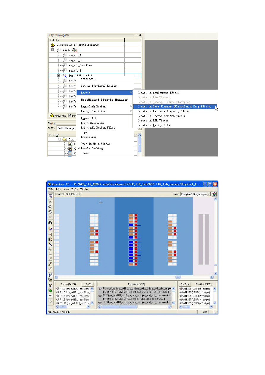
Figure 2.Locating the eight-bit adder in the Chip Editor tool.
Figure 3.The highlighted logic elements for the eight-bit adder.
4
Using the tools described above, and referencing the Data Sheet information for the
Cyclone IV FPGA, describe the eight-bit adder circuit implemented with the lpm add sub
module.
Figure 4.Examining details in a logic element using the Resource Property Editor.
2. Open the Quartus II Compilation Report and and compare the fmax of your adder circuit
with the one designed in Part I. Discuss any differences in performance that are observed.
Part IV
Repeat Part II using the predefined adder circuit called lpm add sub, instead of your
adder-subtractor circuit based on Figure 1. Comment briefly on the circuit structure obtained
using the LPM module, and compare the fmax of this circuit to the one from Part II. Describe
how the lpm add sub module implements the Overflow signal.
5
Part V
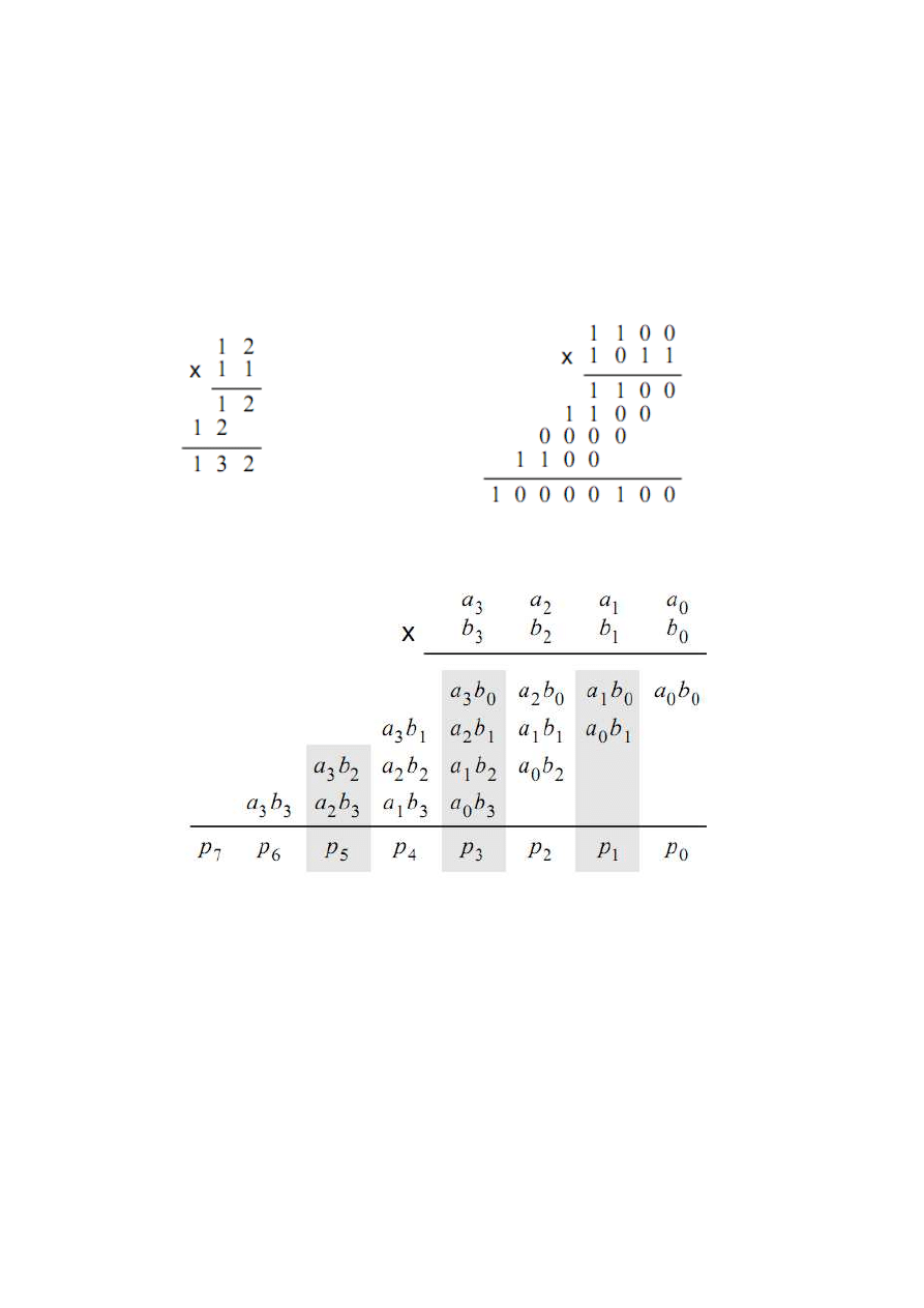
Figure 5a gives an example of the traditional paper-and-pencil multiplication P = A × B,
where A = 12 and B = 11. We need to add two summands that are shifted versions of A to
form the product P = 132. Part b of the figure shows the same example using four-bit binary
numbers. Since each digit in B is either 1 or 0, the summands are either shifted versions of A
or 0000. Figure 5c shows how each summand can be formed by using the Boolean AND
operation of A with the appropriate bit in B.
a) Decimal b) Binary
Figure 5.Multiplication of binary numbers.
6
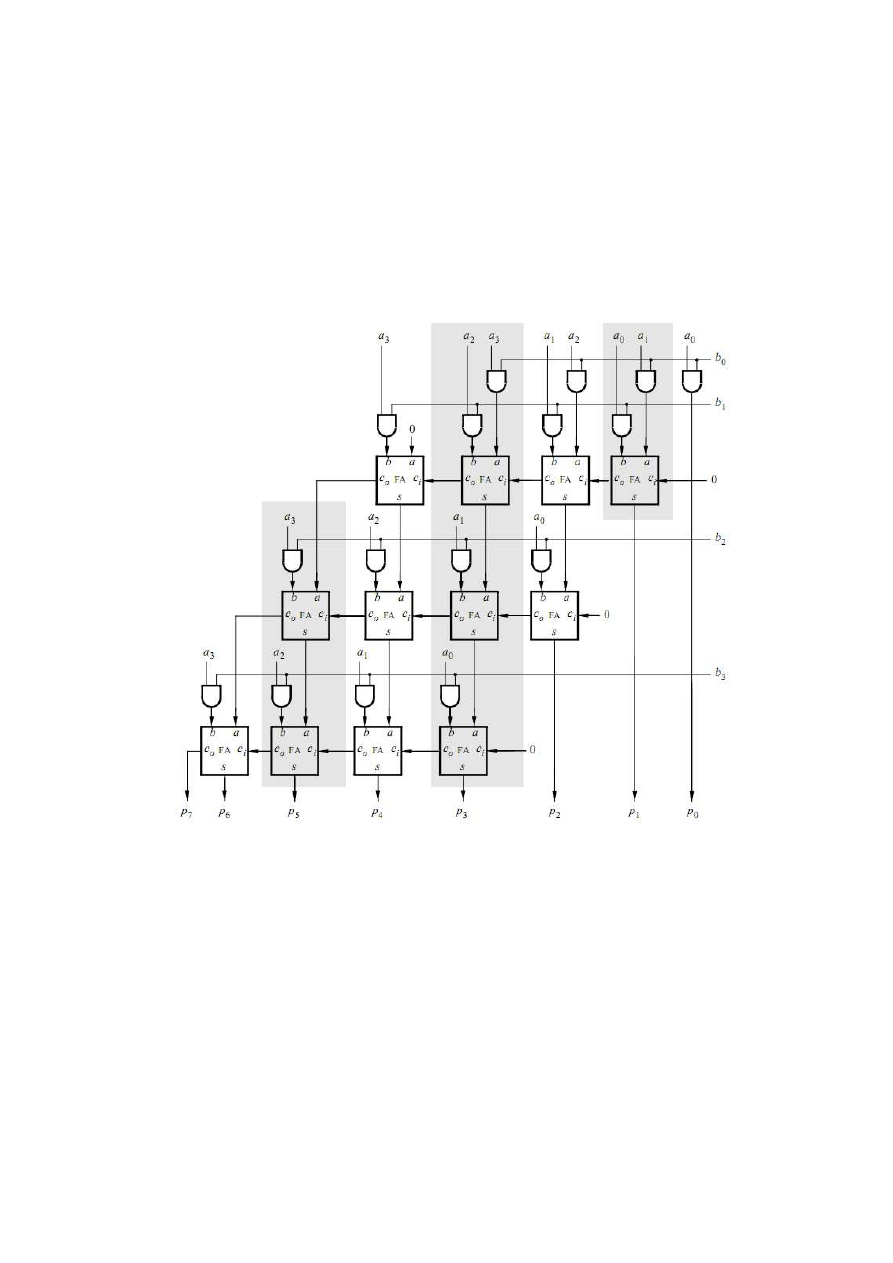
A four-bit circuit that implements P = A × B is illustrated in Figure 6. Because of its regular
structure, this type of multiplier circuit is usually called an array multiplier. The shaded areas in
the circuit correspond to the shaded columns in Figure 5c. In each row of the multiplier AND
gates are used to produce the summands, and full adder modules are used to generate the
required sums.
Figure 6.An array multiplier circuit.
Use the following steps to implement the array multiplier circuit:
1. Create a new Quartus II project which will be used to implement the desired circuit on the
Altera DE2-115 board.
2. Generate the required VHDL file, include it in your project, and compile the circuit.
7

3. Augment your design to use switches SW11−8 to represent the number A and switches
SW3−0 to represent B. The hexadecimal values of A and B are to be displayed on the
7-segment displays HEX6 and HEX4, respectively. The result P = A × B is to be displayed
on HEX1 and HEX0.
4. Assign the pins on the FPGA to connect to the switches and 7-segment displays, as
indicated in the User Manual for the DE2-115 board.
5. Recompile the circuit and download it into the FPGA chip.
6. Test the functionality of your design by toggling the switches and observing the 7-segment
displays.
Part VI
Extend your multiplier to multiply 8-bit numbers and produce a 16-bit product. Use
switches SW 15−8 to represent the number A and switches SW7−0 to represent B. The
hexadecimal values of A and B are to be displayed on the 7-segment displays HEX7−6 and
HEX5−4, respectively. The result P = A × B is to be displayed on HEX3−0. Add registers to
your circuit to store the values of A, B, and the product P , using a similar structure as shown
for the registered adder in Figure 1. After successfully compiling and testing your multiplier
circuit, examine the results produced by the Quartus II Timing Analyzer to determine the fmax
of your circuit. What is the longest path in terms of delay between registers?
Part VII
Change your VHDL code to implement the 8 x 8 multiplier by using the lpm mult module
from the library of parameterized modules in the Quartus II system. Complete the design steps
above. Compare the results in terms of the number of logic elements (LEs) needed and the
circuit fmax.
Part VIII
It many applications of digital circuits it is useful to be able to perform some number of
multiplications and then produce a summation of the results. For this part of the exercise you
are to design a circuit that performs the calculation
S = (A × B) + (C × D)
The inputs A, B, C, and D are eight-bit unsigned numbers, and S provides a 16-bit result. Your
circuit should also provide a carry-out signal, Cout. All of the inputs and outputs of the circuit
should be registered, similar to the structure shown in Figure 1b.
8

1. Create a new Quartus II project which will be used to implement the desired circuit on the
Altera DE2-115 board. Use the lpm mult and lpm add sub modules to realize the
multipliers and adders in your design.
2. Connect the inputs A and C to switches SW15−8 and connect the inputs B and D to
switches SW7−0. Use switch SW16 to select between these two sets of inputs: A, B or C,
D. Also, use the switch SW17 as a write enable (WE) input. Setting WE to 1 should allow
data to be loaded into the input registers when an active clock edge occurs, while setting
WE to 0 should prevent loading of these registers.
3. Use KEY0 as an active-low asynchronous reset input, and use KEY1 as a manual clock
input.
4. Display the hexadecimal value of either A or C, as selected by SW 16, on displays HEX7-6
and display either B or D on HEX5-4. The sum S should be shown on HEX3-0, and the
Coutsignal should appear on LEDG8.
5. Compile your code and use either functional or timing simulation to verify that your circuit
works properly. Then download the circuit onto the DE2-115 board and test its operation.
6. It is often necessary to ensure that a digital circuit is able to meet certain speed
requirements, such as a particular frequency of a signal applied to a clock input. Such
requirements are provided to a CAD system in the form of timing constraints. The
procedure for using timing constraints in the Quartus II CAD system is described in the
tutorial Timing Considerations with VHDL-Based Designs, which is available on the
DE2-115 System CD and in the University Program section of Altera’s web site. For this
exercise we are using a manual clock that is applied by a pushbutton switch, so no
realistic timing requirements exist. But to demonstrate the design issues involved, assume
that your circuit is required to operate with a clock frequency of 220 MHz. Enter this
frequency as a timing constraint in the Quartus II software, and recompile your project.
The Timing Analyzer should report that it is unable to meet the timing requirements due to
the lengths of various register-to-register paths in the circuit. Examine the timing analysis
report and describe briefly the timing violations observed.
7. One way to increase the speed of operation of a given circuit is to insert registers into the
circuit in a way that shortens the lengths of its longest paths. This technique is referred to
as pipelining a circuit, and the inserted registers are often called pipeline registers. Insert
pipeline registers into your design between the multipliers and the adder. Recompile your
project and discuss the results obtained.
9

Part IX
The Quartus II software includes a predesigned module called altmult_add that can
perform calculations of the form S = (A × B) + (C × D). Repeat Part VIII using this module
instead of the lpm_mult and lpm_add_sub modules. Test your circuit using both simulation and
by downloading the circuit onto the DE2-115 board. Briefly describe how the implementation of
your circuit differs when using the altmult_add module. Examine its performance both with and
without the pipeline registers discussed in Part VIII.
Copyright
○
c
2010 Altera Corporation.
10
Wyszukiwarka
Podobne podstrony:
Introduction to VHDL
lab6, SWBlab6
lab1 VHDL
lab6
lab6
lab6 NHIP pyt
lab6 doc
P J Ashenden VHDL tutorial
Lab6 PSN cd 2015
AKiSO lab6
rownania nieliniowe, Automatyka i robotyka air pwr, VI SEMESTR, Notatki.. z ASE, metody numeryczne,
Lab6 5 id 260087 Nieznany
AK lab6 (2)
lab6 7
lab6
konspekt lab6 id 245555 Nieznany
Sprawozdanie EM lab6
lab6, Edukacja, ZiIP, sem. I, Podstawy programowania, Laborki i inne, Podstawy Programowania
więcej podobnych podstron