HCC4051B/52B/53B
HCF4051B/52B/53B
ANALOG MULTIPLEXERS-DEMULTIPLEXERS
.
QUIESCENT CURRENT SPECIFIED TO 20V
FOR HCC DEVICE
.
LOW ”ON” RESISTANCE : 125
Ω
(typ.) OVER
15V p.p. SIGNAL-INPUT RANGE FOR V
DD
-
V
EE
= 15V
.
HIGH ”OFF” RESISTANCE : CHANNEL LEAK-
AGE
±
100pA (typ.) V
DD
– V
EE
= 18V
.
BINARY ADDRESS DECODING ON CHIP
.
VERY LOW QUIESCENT POWER DISSIPA-
TION UNDER ALL DIGITAL CONTROL INPUT
AND SUPPLY CONDITIONS : 0.2
µ
W (typ.),
V
DD
– V
SS
= V
DD
– V
EE
= 10V
.
MATCHED SWITCH CHARACTERISTICS :
R
ON
= 5
Ω
(typ.) for V
DD
– V
EE
= 15V
.
WIDE RANGE OF DIGITAL AND ANALOG SIG-
NAL LEVELS : DIGITAL 3 TO 20V, ANALOG TO
20V p.p.
.
5V, 10V, AND 15V PARAMETRIC RATINGS
.
INPUT CURRENT OF 100mA AT 18V AND
25
°
C FOR HCC DEVICE
.
100% TESTED FOR QUIESCENT CURRENT
.
MEETS ALL REQUIREMENTS OF JEDEC TEN-
TATIVE STANDARD N
o
13A, ”STANDARD
SPECIFICATIONS FOR DESCRIPTION OF ”B”
SERIES CMOS DEVICES”
4051B - SINGLE 8-CHANNEL
4052B - DIFFERENTIAL 4-CHANNEL
4053B - TRIPLE 2-CHANNEL
June 1989
The HCC 4051B, 4052B and 4053B (extended tem-
perature range) and HCF4051B, 4052B and 4053B
(intermediate temperature range) are monolithic in-
tegrated circuits, available in 16-lead dual in-line
plastic or ceramic package and plastic micropack-
age.
HCC/HCF4051B,
HCC/HCF4052B,
and
HCC/HCF4053B
analog
multiplexers/demulti-
plexers are digitally controlled analog switches hav-
ing low ON impedance and very low OFF leakage
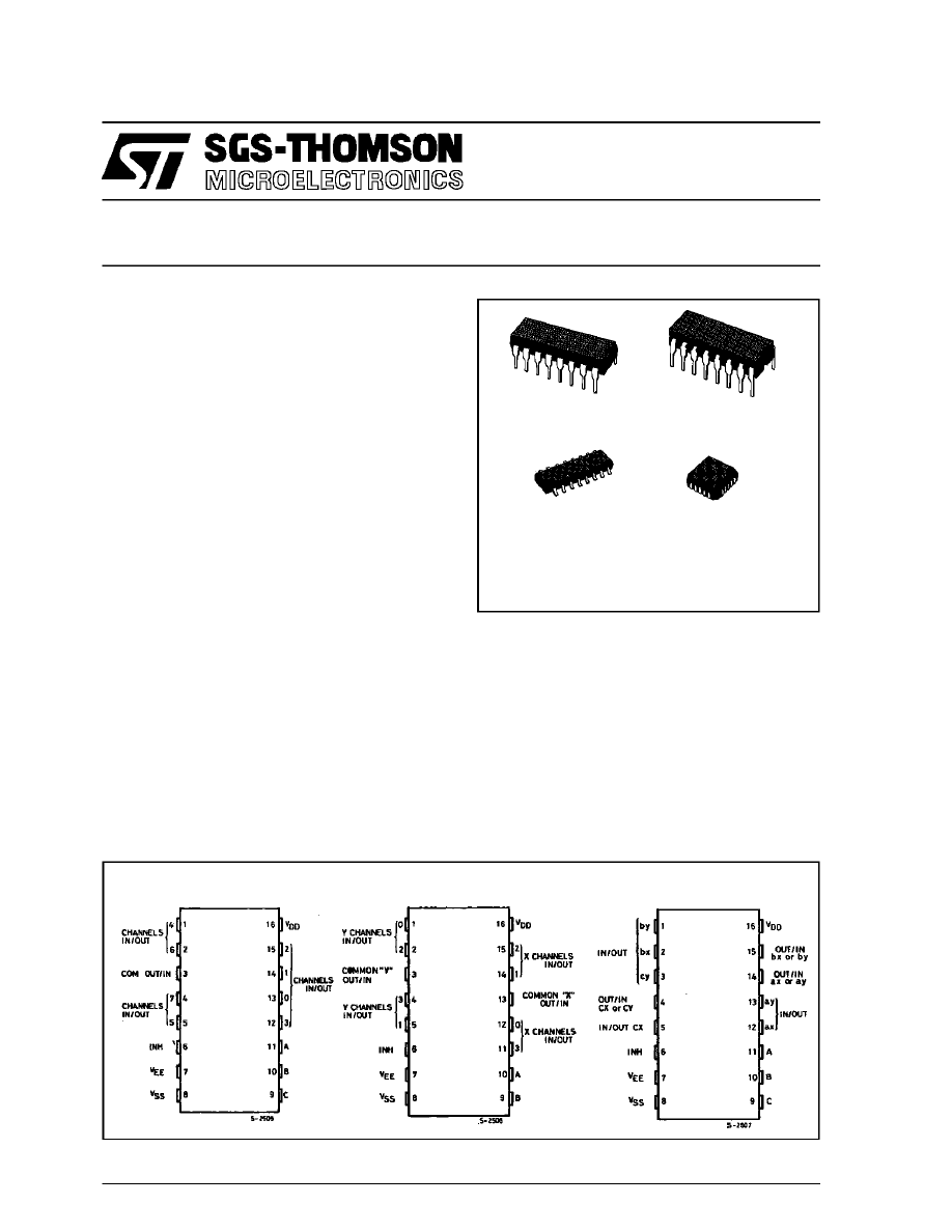
PIN CONNECTIONS
EY
(Plastic Package)
F
(Ceramic Frit Seal Package)
M1
(Micro Package)
C1
(Plastic Chip Carrier)
ORDER CODES :
HCC40XXBF
HCF40XXBM1
HCF40XXBEY
HCF40XXBC1
4051B
4052B
4053B
DESCRIPTION
1/17
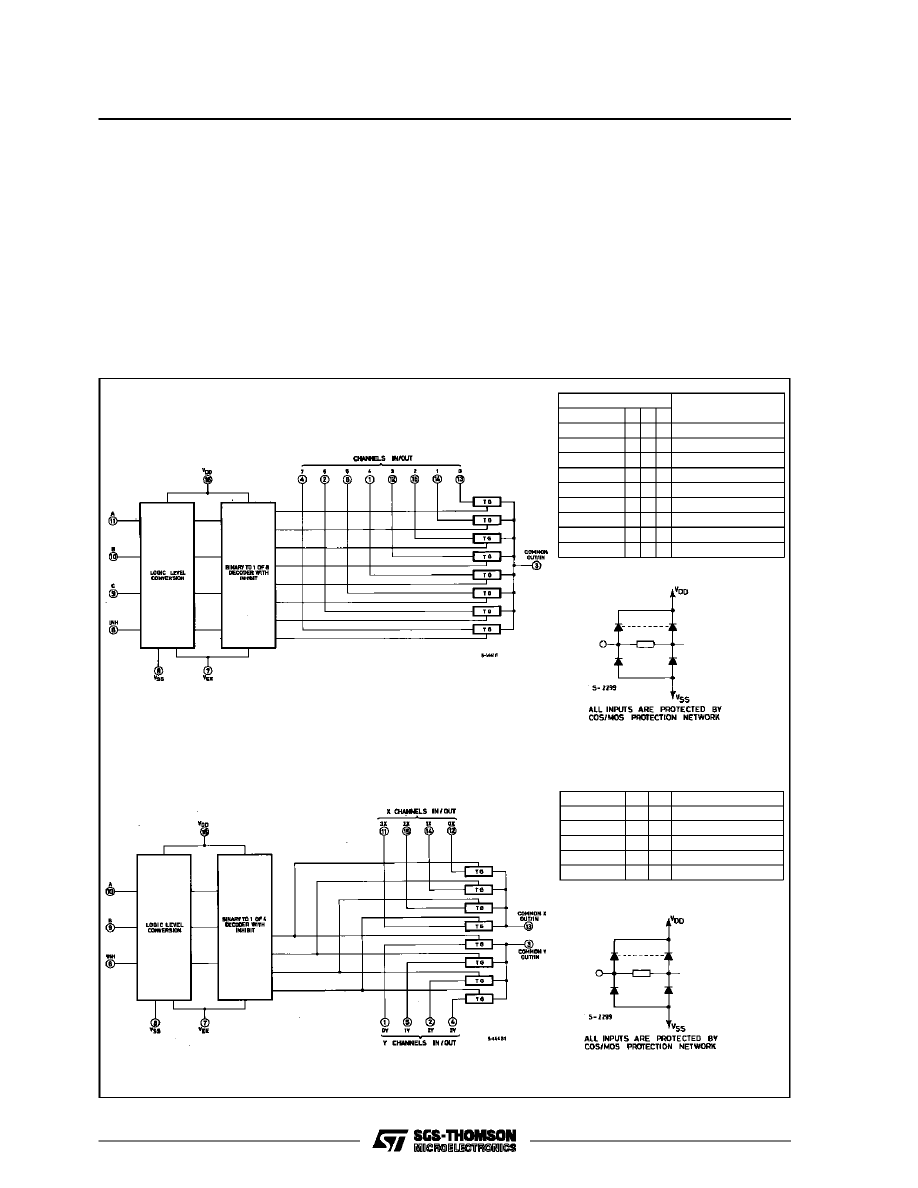
FUNCTIONAL DIAGRAMS AND TRUTH TABLES
current. These multiplexer circuits dissipate ex-
tremely low quiescent power over the full V
DD
– V
SS
and V
DD
– V
EE
supply-voltage ranges, independent
of the logic state of the control signals. When a-logic
”1” is present at the inhibit input terminal all channel
are off. The HCC/HCF4051B is a single 8-channel
multiplexer having three binary control inputs, A, B,
and C, and an inhibit input. The three binary signals
select 1 of 8 channels to be turned on, and connect
one
of
the
8
inputs
to
the
output.
The
HCC/HCF4052B is a differential 4-channel multi-
plexer having two binary control inputs, A and B, and
an inhibit input. The two binary input signals select
1 of 4 pairs of channels to be turned on and connect
the
analog
inputs
to
the
outputs.
The
HCC/HCF4053B is a triple 2-channel multiplexer
having three separate digital control inputs, A, B,
and C, and an inhibit input. Each control input se-
lects one of a pair of channels which are connected
in a singlepole double-throw configuration.
Input States
Inhibit
C
B
A
”On” Channel (S)
0
0
0
0
0
0
0
0
1
1
0
0
1
0
2
0
0
1
1
3
0
1
0
0
4
0
1
0
1
5
0
1
1
0
6
0
1
1
1
7
1
X
X
X
None
4052B
Inhibit
B
A
0
0
0
0x, 0y
0
0
1
1x, 1y
0
1
0
2x, 2y
0
1
1
3x, 3y
1
X
X
None
4051B
HCC/HCF4051B/52B/53B
2/17
ABSOLUTE MAXIMUM RATINGS
Symbol
Parameter
Value
Unit
V
DD
*
Supply Voltage : HC C Types
H C F Types
– 0.5 to + 20
– 0.5 to + 18
V
V
V
i
Input Voltage
– 0.5 to V
DD
+ 0.5
V
I
I
DC Input Current (any one input)
±
10
mA
P
t o t
Total Power Dissipation (per package)
Dissipation per Output Transistor
for T
o p
= Full Package-temperature Range
200
100
mW
mW
T
o p
Operating Temperature : HCC Types
H CF Types
– 55 to + 125
– 40 to + 85
°
C
°
C
T
s t g
Storage Temperature
– 65 to + 150
°
C
RECOMMENDED OPERATING CONDITIONS
Symbol
Parameter
Value
Unit
V
DD
Supply Voltage : HC C Types
H C F Types
3 to 18
3 to 15
V
V
V
I
Input Voltage
0 to V
DD
V
T
o p
Operating Temperature : H CC Types
H C F Types
– 55 to + 125
– 40 to + 85
°
C
°
C
Stresses above those listed under ”Absolute Maximum Ratings” may cause permanent damage to the device. This is a stress
rating only and functional operation of the device at these or any other conditions above those indicated in the operational sec-
tions of this specifi cation is not implied. Exposure to absolute maximum rating conditions for external periods may affect device
reliability.
* All voltage values are referred to V
SS
pin voltage.
Inhibit
A or B
or C
0
0
ax or bx or cx
0
1
ay or by or cy
1
X
None
FUNCTIONAL DIAGRAMS AND TRUTH TABLES (continued)
4053
X = Don’t care.
HCC/HCF4051B/52B/53B
3/17
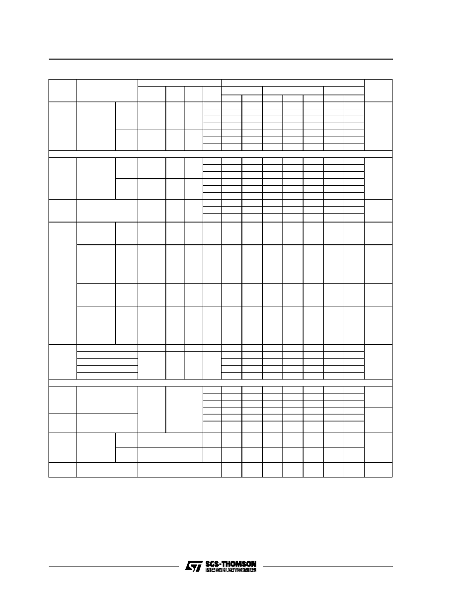
STATIC ELECTRICAL CHARACTERISTICS (over recommended operating conditions)
Test Conditions
Val ue
V
IS
V
EE
V
SS
V
DD
T
Lo w
*
2 5
°
C
T
High
*
Symbol
Parameter
(V)
(V)
(V)
(V)
Min.
Max.
Min.
Typ.
Max.
Min.
Max.
Unit
I
L
Quiescent
Device
Current
HCC
Types
5
5
0.04
5
150
µ
A
10
10
0.04
10
300
15
20
0.04
20
600
20
100
0.08
100
3000
HCF
Types
5
20
0.04
20
150
10
40
0.04
40
300
15
80
0.04
80
600
SWITCH
ON
Resistance
HCC
Types
0
≤
V
I
≤
V
DD
0
0
5
880
470
1050
1200
Ω
10
310
180
400
580
15
220
125
280
400
HCF
Types
0
≤
V
I
≤
V
DD
0
0
5
880
470
1050
1200
10
330
180
400
520
15
230
125
280
360
∆
ON
Resistance
∆
R
ON
(between any 2
channels)
0
0
5
10
Ω
10
10
15
5
OFF (
•
)
Channel
Leakage
Current
Any
Channel
OFF
HCC
Types
0
0
18
100
±
0.1
100
1000
nA
All
Channels
OFF
(common
OUT/IN)
HCC
Types
0
0
18
100
±
0.1
100
1000
nA
Any
Channel
OFF
HCF
Types
0
0
15
300
±
0.1
300
1000
nA
All
Channels
OFF
(common
OUT/IN)
HCF
Types
0
0
15
300
±
0.1
300
1000
nA
C
Capaci-
tance
Input
5
pF
Output 4051
– 5
– 5
5
30
Output 4052
18
Output 4053
9
Feedthrough
0.2
CONTROL (Address or Inhibit)
V
IL
Input Low Voltage
= V
DD
Thru
1K
Ω
V
EE
= V
SS
R
L
= 1K
Ω
to V
SS
I
IS
< 2
µ
A
(on all off
channels)
5
1.5
1.5
1.5
V
10
3
3
3
15
4
4
4
V
IH
Input High Voltage
5
3.5
3.5
3.5
V
10
7
7
7
15
11
11
11
I
IH
, I
IL
Input
Leakage
Current
HCC
Types
V
I
= 0/18V
18
±
0. 1
±
10
–3
±
0.1
±
1
µ
A
HCF
Types
V
I
= 0/15V
15
±
0. 3
±
10
–3
±
0.3
±
1
C
I
Input Capacitance
Any Address or Inhibit
Input
5
7.5
pF
(
•
) Determined by minimum feasible leakage measurement for automatic testing.
(*) T
Low
= – 55
°
C for HCC device : – 40
°
C for HCF device.
(*) T
High
= + 125
°
C for HCC device : + 85
°
C for HCF device.
HCC/HCF4051B/52B/53B
4/17
DYNAMIC ELECTRICAL CHARACTERISTICS
(T
am b
= 25
°
C, C
L
= 50pF all input square wave rise and fall time = 20ns)
Test Conditions
Val ue
Parameter
V
EE
(V)
R
L
(k
Ω
)
f
i
(kHz)
V
IS
(V)
V
S S
(V)
V
DD
(V)
Typ. Max.
Unit
SWI TCH
t
p d
Propagation Delay Time
(signal input to output)
200
10 V
_I
__
I_
5
30
30
ns
10
15
60
15
11
20
Frequency Response
Channel ”ON” (sine wave
input)
= V
S S
1
5 (
•
)
10
V
o
at Common
OUT/IN
4053B
30
MHz
4052B
25
4051B
20
V
o
at 20 Log
= – 3dB
__
V
I
V
o
at any Channel
60
Feedthrough (all channels
OFF)
= V
S S
1
5 (
•
)
10
V
o
at Common
OUT/IN
4053
8
MHz
4052
10
4051
12
V
o
at 20 Log
= – 40dB
__
V
I
V
o
at any Channel
8
Frequency Signal Crosstalk
Between any 2 Channels
3
V
o
at 20 Log
= – 40dB
__
V
I
= V
S S
1
5 (
•
)
10
Between Sections
4052B only
measured
o n
common
6
MHz
MHz
measured
on any
channel
10
Between any 2
Sections 4053B
only
in Pin 2
out Pin 14
2.5
in Pin 15
out Pin 14
6
Sine Wave Distortion
f
i s
= 1kHz Sine Wave
= V
S S
10
1
2 (
•
)
5
0.3
%
10
1
3 (
•
)
10
0.2
10
1
5 (
•
)
15
0.12
CONTROL (Address or Inhibit)
Progation Delay Time :
Address-to Signal OUT
Channels ON or OFF
0
0
5
360
720
ns
0
0
10
160
320
0
0
15
120
240
– 5
0
5
225
450
Propagation Delay Time :
Inhibit to Signal OUT
(channel turning ON)
0
10
0
5
360
720
ns
0
0
10
160
320
0
0
15
120
240
– 10
0
5
200
400
Propagation Delay Time :
Inhibit to Signal OUT
(channel turning OFF)
0
0.3
5
200
450
ns
0
10
90
210
0
15
70
160
– 10
5
130
300
Address or Inhibit to Signal
Crosstalk
0
10*
0
10
V
C
= V
DD
–V
SS
(square
wave)
65
mV
peak
(
•
) Peak to peak voltage symmetrical about V
DD
-V
EE
2
(*) Both ends of channel.
HCC/HCF4051B/52B/53B
5/17
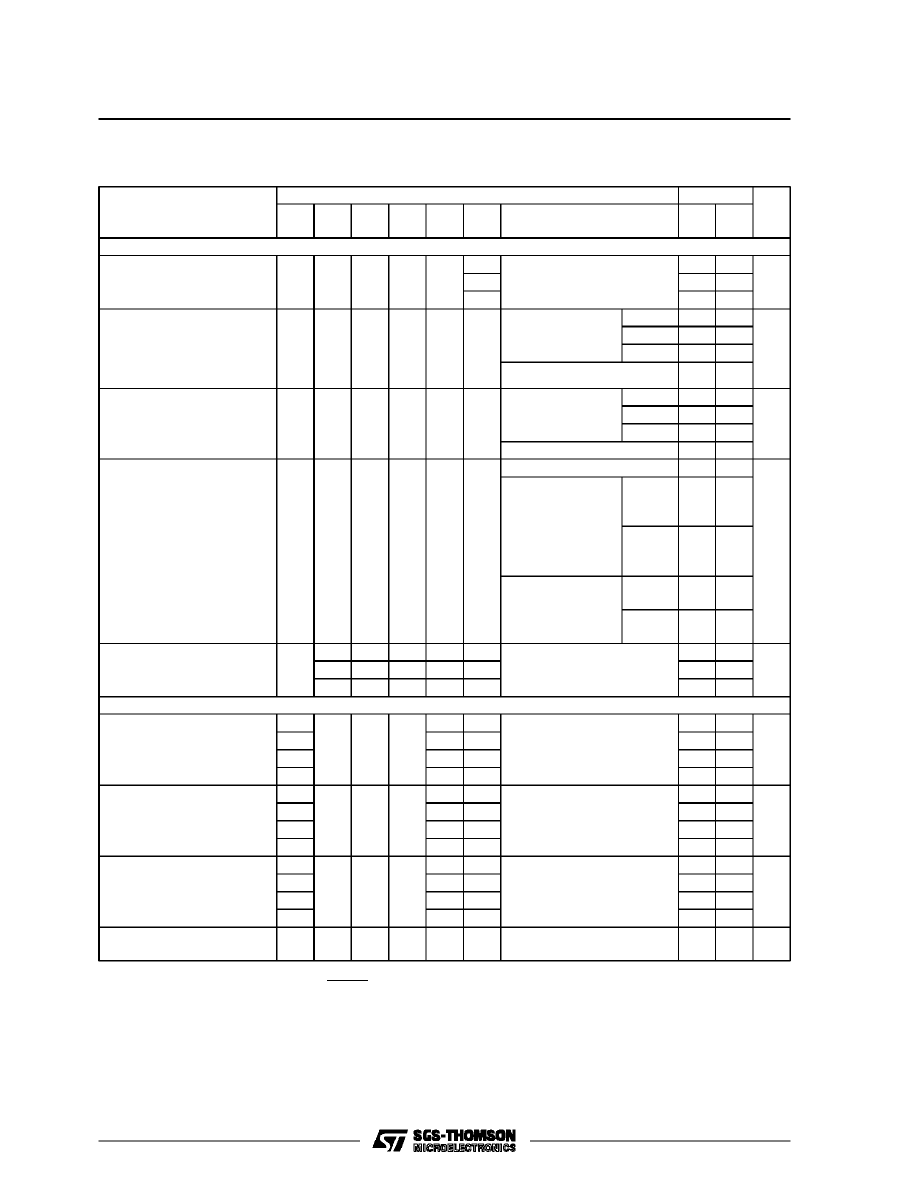
Typical Channel ON Resistance vs. Input Signal
Voltage (all types).
Typical Channel ON Resistance vs. Input Signal
Voltage (all types).
Typical Channel ON Resistance vs. Input Signal
Voltage (all types).
Typical Channel ON Resistance vs. Input Signal
Voltage (all types).
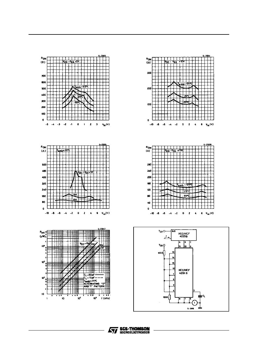
Typical Dynamic Power Dissipation/Package vs. Switching Frequency and Test Circuit (4051B).
HCC/HCF4051B/52B/53B
6/17
Typical ON Characteristics for 1 of 8 Channels
(4051B).
Typical Dynamic Power Dissipation/Package vs. Switching Frequency and Test Circuit (4052B).
Typical Dynamic Power Dissipation/Package vs. Switching Frequency and Test Circuit (4053B).
HCC/HCF4051B/52B/53B
7/17
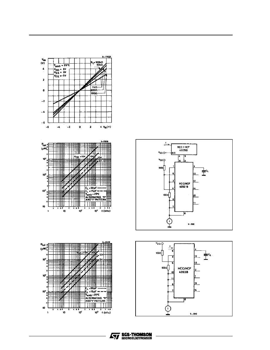
Channel Being Turned ON (R
L
= 10K
Ω
).
Channel Being Turned OFF (R
L
= 300K
Ω
).
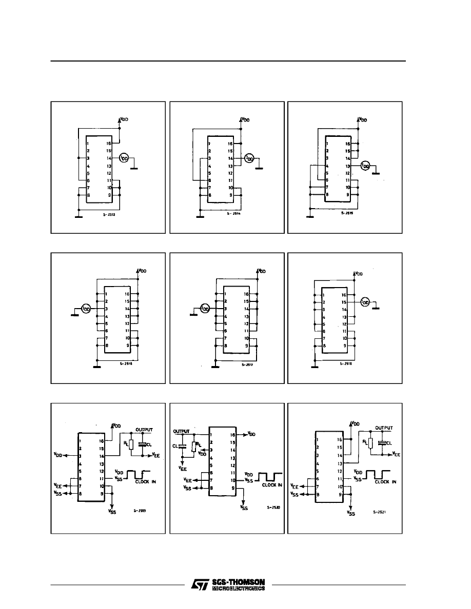
TYPICAL BIAS VOLTAGES
Fig. (a)
Fig. (b)
Fig. (c)
Fig. (d)
The ADDRESS (digital-control inputs) and INHIBIT logic levels are : ”0”=V
SS
and ”1”=V
DD
. The analog signal (trough the TG)
may swing from V
EE
to V
DD
.
WAVEFORMS
HCC/HCF4051B/52B/53B
8/17
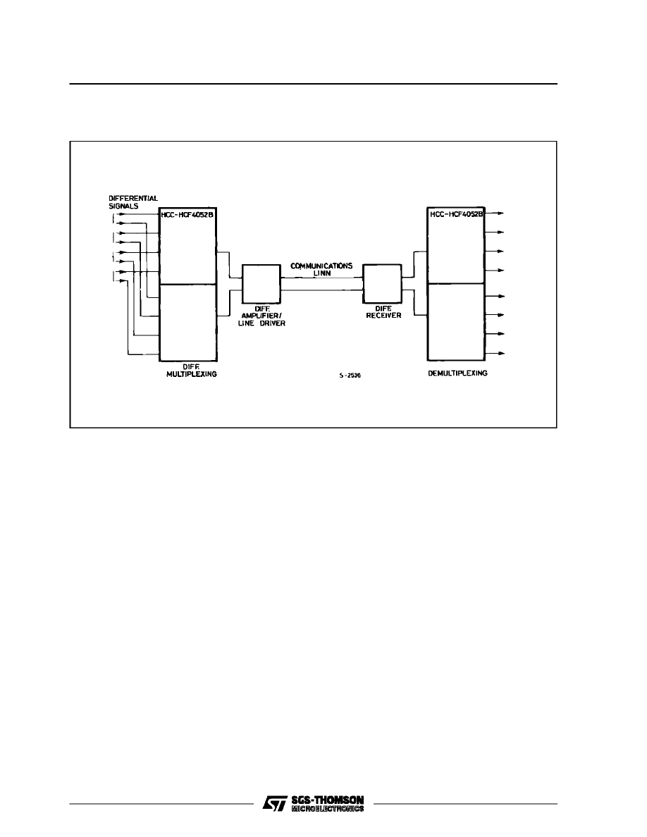
TYPICAL APPLICATIONS
TYPICAL TIME-DIVISION APPLICATION OF THE 4052B
Control of analog signals up to 20V peak-to-peak
can be achieved by digital signal amplitudes of 4.5
to 20V (if V
DD
– V
SS
= 3V, a V
DD
– V
EE
of up to 13V
can be controlled ; for V
DD
– V
EE
level differences
above 13V, a V
DD
– V
SS
of at least 4.5V is required).
For example, if V
DD
= + 5V, V
SS
= 0, and V
EE
=
–13.5V, analog signals from – 13.5V to + 4.5V can
be controlled by digital inputs of 0 to 4.5V. In certain
applications, the external load-resistor current may
include both V
DD
and signal-line components. To
avoid drawing V
DD
current when switch current
flows into the transmission gate inputs, the voltage
drop across the bidirectional switch must not exceed
0,8 volt (valvulated from R
ON
values shown in
ELECTRICAL CHARACTERISTICS CHART). No
V
DD
current will flow through R
L
if the switch current
flows into lead 3 on the HCC/HCF4051 ; leads 3 and
13 on the HCC/HCF4052 ; leads 4, 14, and 15 on
the HCC/HCF4053.
SPECIAL CONSIDERATIONS
HCC/HCF4051B/52B/53B
9/17
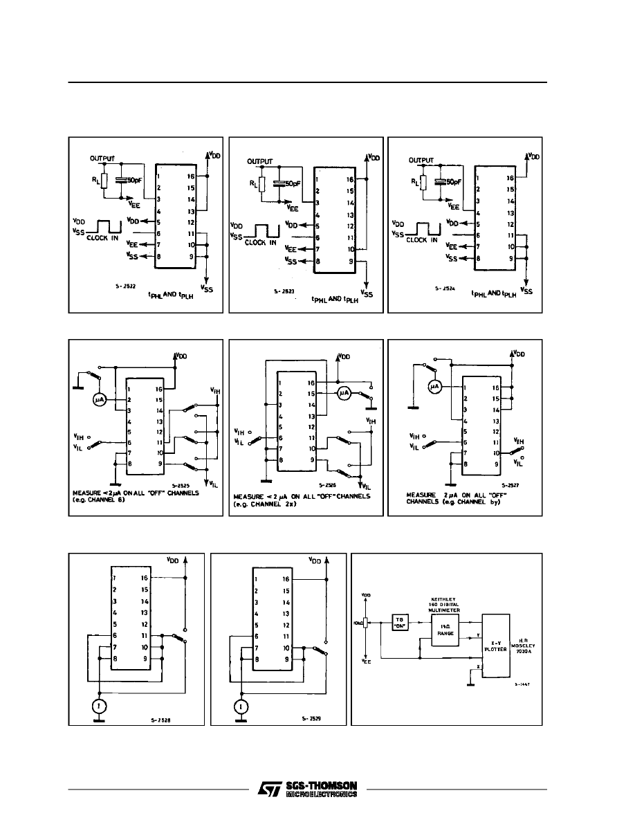
Off Channel Leakage Current-any Channel OFF.
TEST CIRCUITS
Off Channel Leakage Current-all Channel OFF.
4051
4052
4053
4051
4052
4053
Propagation Delay-adress Input to Signal Output.
4051
4053
4052
HCC/HCF4051B/52B/53B
10/17
Propagation Delay-Inhibit Input to Signal Output.
TEST CIRCUITS (continued)
Input Voltage.
4051
4052
4053
4051
4052
4053
4051
4053
4052
Quiescent Device Current.
Channel ON Resistance
Meaurement Circuit.
HCC/HCF4051B/52B/53B
11/17
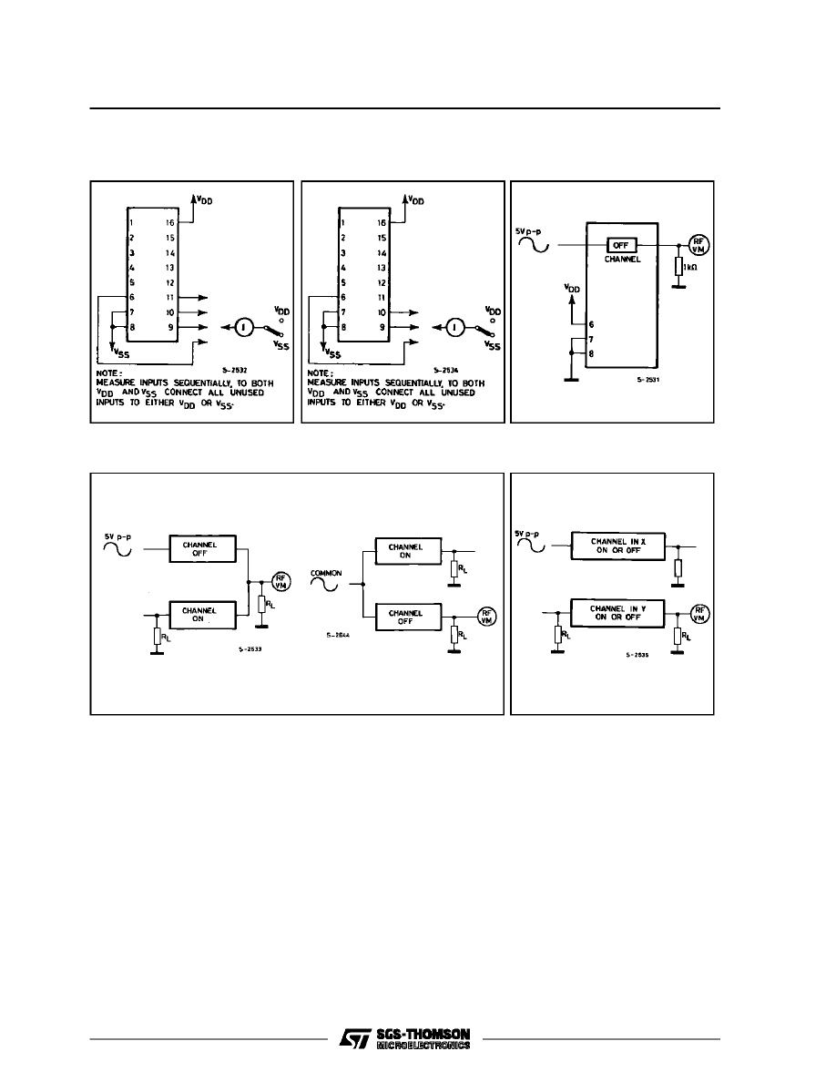
Input Current.
TEST CIRCUITS (continued)
Crosstalk Betwen any two Channels (All Types).
Feedthrough (All Types).
Crosstalk Betweenn Duals or Tri-
plets (4052-4053).
4052
4051 - 4053
HCC/HCF4051B/52B/53B
12/17
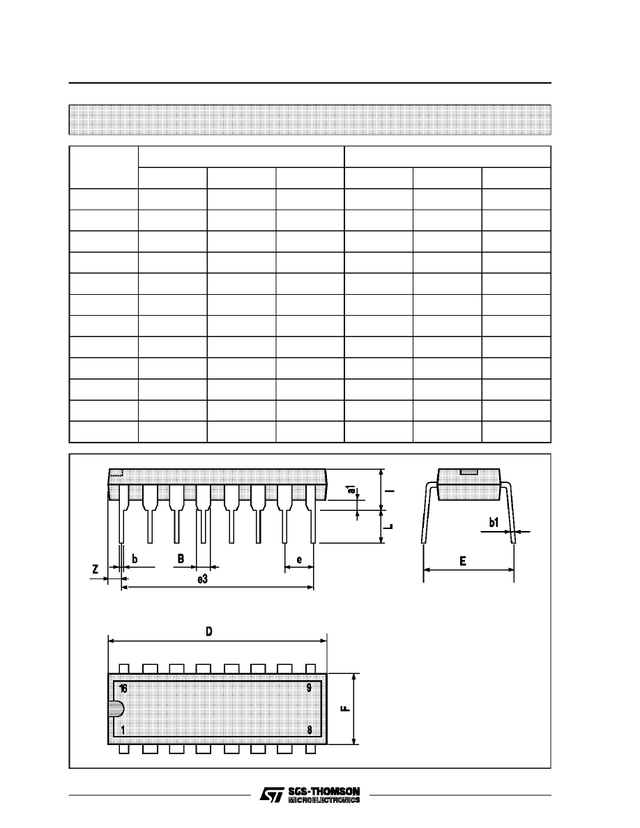
Plastic DIP16 (0.25) MECHANICAL DATA
DIM.
mm
inch
MIN.
TYP.
MAX.
MIN.
TYP.
MAX.
a1
0.51
0.020
B
0.77
1.65
0.030
0.065
b
0.5
0.020
b1
0.25
0.010
D
20
0.787
E
8.5
0.335
e
2.54
0.100
e3
17.78
0.700
F
7.1
0.280
I
5.1
0.201
L
3.3
0.130
Z
1.27
0.050
P001C
HCC/HCF4051B/52B/53B
13/17
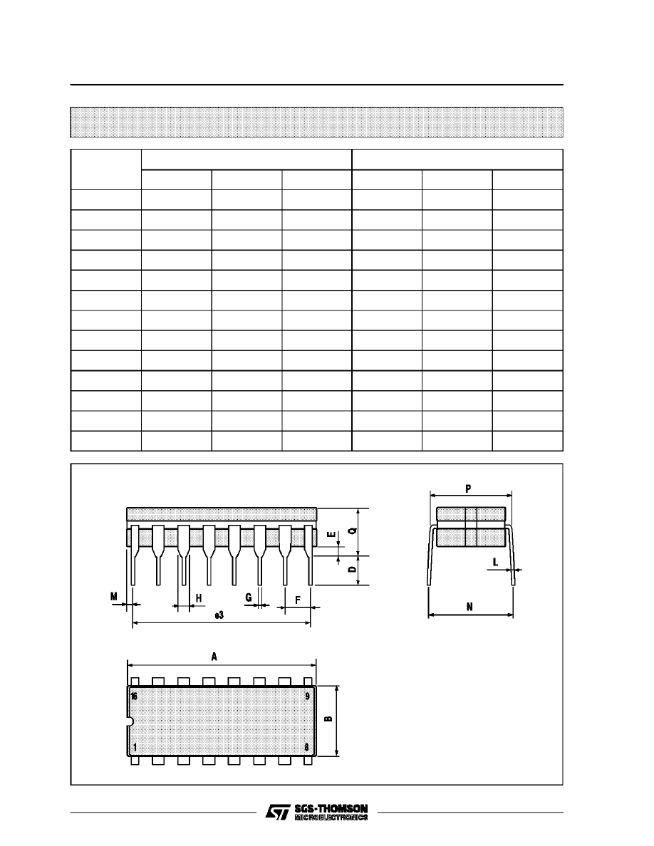
Ceramic DIP16/1 MECHANICAL DATA
DIM.
mm
inch
MIN.
TYP.
MAX.
MIN.
TYP.
MAX.
A
20
0.787
B
7
0.276
D
3.3
0.130
E
0.38
0.015
e3
17.78
0.700
F
2.29
2.79
0.090
0.110
G
0.4
0.55
0.016
0.022
H
1.17
1.52
0.046
0.060
L
0.22
0.31
0.009
0.012
M
0.51
1.27
0.020
0.050
N
10.3
0.406
P
7.8
8.05
0.307
0.317
Q
5.08
0.200
P053D
HCC/HCF4051B/52B/53B
14/17
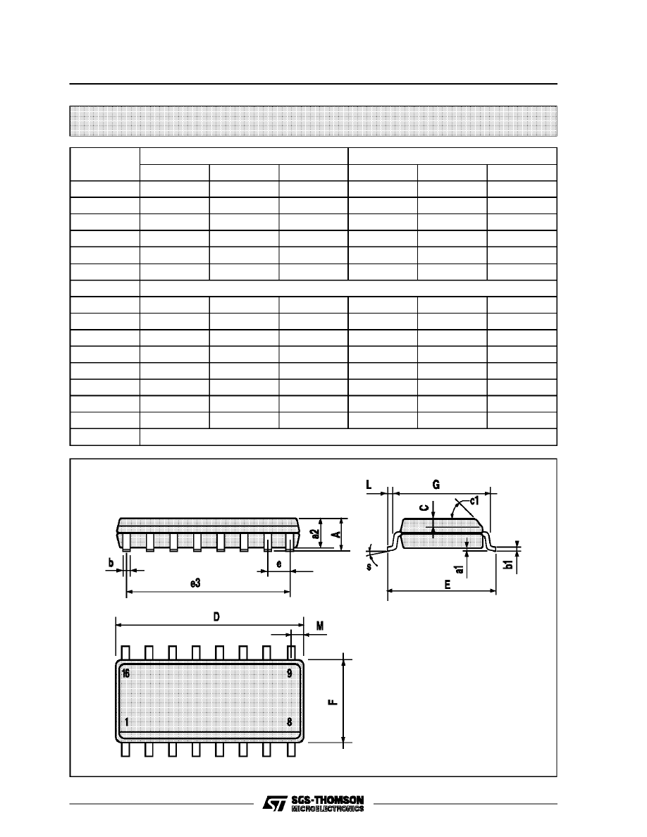
SO16 (Narrow) MECHANICAL DATA
DIM.
mm
inch
MIN.
TYP.
MAX.
MIN.
TYP.
MAX.
A
1.75
0.068
a1
0.1
0.2
0.004
0.007
a2
1.65
0.064
b
0.35
0.46
0.013
0.018
b1
0.19
0.25
0.007
0.010
C
0.5
0.019
c1
45
°
(typ.)
D
9.8
10
0.385
0.393
E
5.8
6.2
0.228
0.244
e
1.27
0.050
e3
8.89
0.350
F
3.8
4.0
0.149
0.157
G
4.6
5.3
0.181
0.208
L
0.5
1.27
0.019
0.050
M
0.62
0.024
S
8
°
(max.)
P013H
HCC/HCF4051B/52B/53B
15/17
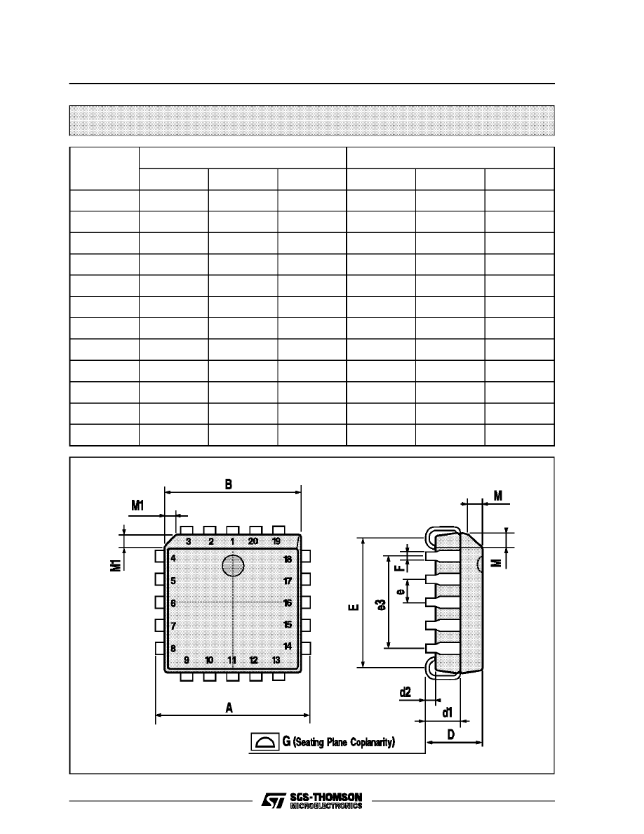
PLCC20 MECHANICAL DATA
DIM.
mm
inch
MIN.
TYP.
MAX.
MIN.
TYP.
MAX.
A
9.78
10.03
0.385
0.395
B
8.89
9.04
0.350
0.356
D
4.2
4.57
0.165
0.180
d1
2.54
0.100
d2
0.56
0.022
E
7.37
8.38
0.290
0.330
e
1.27
0.050
e3
5.08
0.200
F
0.38
0.015
G
0.101
0.004
M
1.27
0.050
M1
1.14
0.045
P027A
HCC/HCF4051B/52B/53B
16/17
Information furnished is believed to be accurate and reliable. However, SGS-THOMSON Microelectronics assumes no responsability for the
consequences of use of such information nor for any infringement of patents or other rights of third parties which may results from its use. No
license is granted by implication or otherwise under any patent or patent rights of SGS-THOMSON Microelectronics. Specifications mentioned
in this publication are subject to change without notice. This publication supersedes and replaces all information previously supplied.
SGS-THOMSON Microelectronics products are not authorized for use as critical components in life support devices or systems without express
written approval of SGS-THOMSON Microelectonics.
1994 SGS-THOMSON Microelectronics - All Rights Reserved
SGS-THOMSON Microelectronics GROUP OF COMPANIES
Australia - Brazil - France - Germany - Hong Kong - Italy - Japan - Korea - Malaysia - Malta - Morocco - The Netherlands -
Singapore - Spain - Sweden - Switzerland - Taiwan - Thailand - United Kingdom - U.S.A
HCC/HCF4051B/52B/53B
17/17
Wyszukiwarka
Podobne podstrony:
Abolicja podatkowa id 50334 Nieznany (2)
4 LIDER MENEDZER id 37733 Nieznany (2)
katechezy MB id 233498 Nieznany
metro sciaga id 296943 Nieznany
perf id 354744 Nieznany
interbase id 92028 Nieznany
Mbaku id 289860 Nieznany
Probiotyki antybiotyki id 66316 Nieznany
miedziowanie cz 2 id 113259 Nieznany
LTC1729 id 273494 Nieznany
D11B7AOver0400 id 130434 Nieznany
analiza ryzyka bio id 61320 Nieznany
pedagogika ogolna id 353595 Nieznany
Misc3 id 302777 Nieznany
cw med 5 id 122239 Nieznany
D20031152Lj id 130579 Nieznany
mechanika 3 id 290735 Nieznany
więcej podobnych podstron