
PHT6N06T
TrenchMOS™ standard level FET
Rev. 02 — 03 February 2003
Product data
M3D087
1.
Product profile
1.1 Description
N-channel enhancement mode field-effect transistor in a plastic package using
TrenchMOS™ technology.
Product availability:
PHT6N06T in SOT223.
1.2 Features
1.3 Applications
1.4 Quick reference data
2.
Pinning information
■
Low on-state resistance
■
Low Q
GD
■
Fast switching
■
Surface mounting package.
■
DC to DC converters
■
General purpose switching.
■
V
DS
≤
55 V
■
I
D
≤
5.5 A
■
P
tot
≤
8.3 W
■
R
DSon
≤
150 m
Ω
Table 1:
Pinning - SOT223, simplified outline and symbol
Pin
Description
Simplified outline
Symbol
1
gate (g)
SOT223
2
drain (d)
3
source (s)
4
drain (d)
4
1
2
3
MSB002 - 1
Top view
s
d
g
MBB076

Philips Semiconductors
PHT6N06T
TrenchMOS™ standard level FET
Product data
Rev. 02 — 03 February 2003
2 of 12
9397 750 10633
© Koninklijke Philips Electronics N.V. 2003. All rights reserved.
3.
Limiting values
Table 2:
Limiting values
In accordance with the Absolute Maximum Rating System (IEC 60134).
Symbol Parameter
Conditions
Min
Max
Unit
V
DS
drain-source voltage (DC)
25
°
C
≤
T
j
≤
150
°
C
-
55
V
V
DGR
drain-gate voltage (DC)
25
°
C
≤
T
j
≤
150
°
C; R
GS
= 20 k
Ω
-
55
V
V
GS
gate-source voltage (DC)
-
±
20
V
I
D
drain current (DC)
T
sp
= 25
°
C; V
GS
= 10 V;
and
-
5.5
A
T
sp
= 100
°
C; V
GS
= 10 V;
-
3.8
A
I
DM
peak drain current
T
sp
= 25
°
C; pulsed; t
p
≤
10
µ
s;
-
22
A
P
tot
total power dissipation
T
sp
= 25
°
C;
-
8.3
W
T
stg
storage temperature
−
55
+150
°
C
T
j
junction temperature
−
55
+150
°
C
Source-drain diode
I
S
source (diode forward) current (DC)
T
sp
= 25
°
C
-
5.5
A
I
SM
peak source (diode forward) current T
sp
= 25
°
C; pulsed; t
p
≤
10
µ
s
-
22
A
Philips Semiconductors
PHT6N06T
TrenchMOS™ standard level FET
Product data
Rev. 02 — 03 February 2003
3 of 12
9397 750 10633
© Koninklijke Philips Electronics N.V. 2003. All rights reserved.
V
GS
≥
10 V
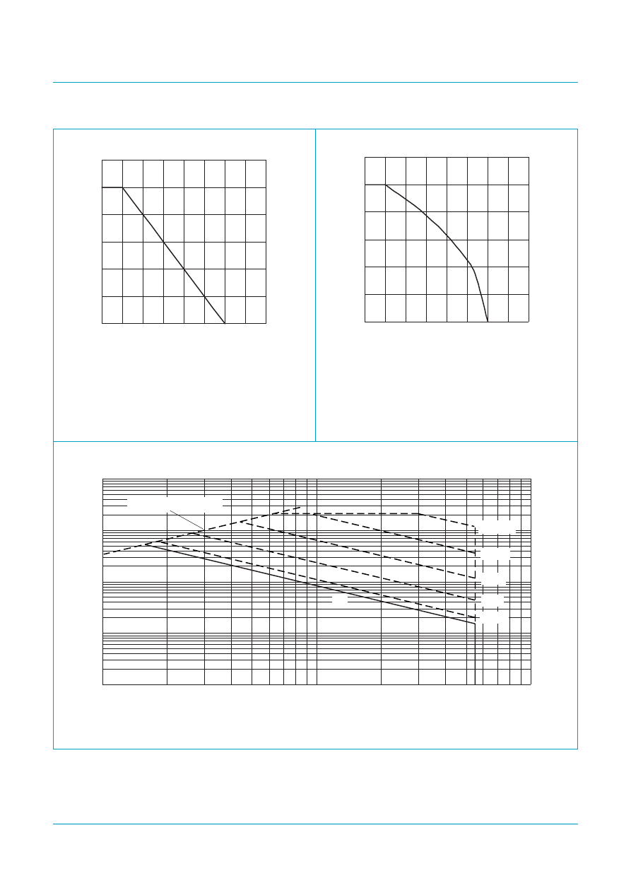
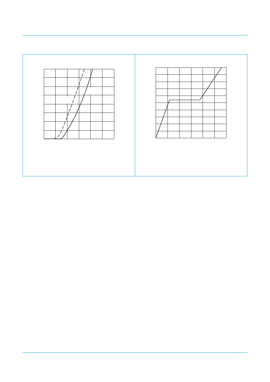
Fig 1.
Normalized total power dissipation as a
function of solder point temperature.
Fig 2.
Normalized continuous drain current as a
function of solder point temperature.
T
sp
= 25
°
C; I
DM
is single pulse; V
GS
= 10 V.
Fig 3.
Safe operating area; continuous and peak drain currents as a function of drain-source voltage.
03aa17
0
40
80
120
0
50
100
150
200
(%)
Tsp (
°
C)
Pder
03aa25
0
40
80
120
0
50
100
150
200
Tsp (
°
C)
Ider
(%)
P
der
P
tot
P
tot 25 C
°
(
)
-----------------------
100%
×
=
I
der
I
D
I
D 25 C
°
(
)
-------------------
100%
×
=
003aaa313
10-2
10-1
1
10
102
1
10
102
VDS (V)
ID
DC
Limit RDSon = VDS/ID
(A)
tp = 10
µ
s
100
µ
s
1 ms
10 ms
100 ms
Philips Semiconductors
PHT6N06T
TrenchMOS™ standard level FET
Product data
Rev. 02 — 03 February 2003
4 of 12
9397 750 10633
© Koninklijke Philips Electronics N.V. 2003. All rights reserved.
4.
Thermal characteristics
4.1 Transient thermal impedance
Table 3:
Thermal characteristics
Symbol Parameter
Conditions
Min
Typ
Max
Unit
R
th(j-sp)
thermal resistance from junction to solder point
-
-
15
K/W
R
th(j-a)
thermal resistance from junction to ambient
minimum footprint; mounted on a
printed-circuit board
-
70
-
K/W
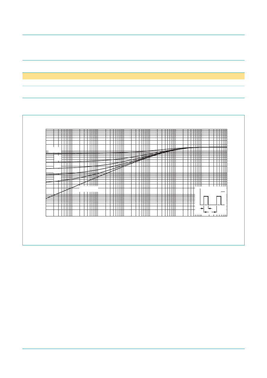
Fig 4.
Transient thermal impedance from junction to solder point as a function of pulse duration.
003aaa314
single pulse
0.2
0.1
0.05
0.02
10-2
10-1
1
10
102
10-6
10-5
10-4
10-3
10-2
10-1
1
10
tp (s)
Zth(j-sp)
(K/W)
δ
= 0.5
tp
tp
T
P
t
T
δ
=

Philips Semiconductors
PHT6N06T
TrenchMOS™ standard level FET
Product data
Rev. 02 — 03 February 2003
5 of 12
9397 750 10633
© Koninklijke Philips Electronics N.V. 2003. All rights reserved.
5.
Characteristics
Table 4:
Characteristics
T
j
= 25
°
C unless otherwise specified.
Symbol Parameter
Conditions
Min
Typ
Max
Unit
Static characteristics
V
(BR)DSS
drain-source breakdown voltage
I
D
= 250
µ
A; V
GS
= 0 V
T
j
= 25
°
C
55
-
-
V
T
j
=
−
55
°
C
50
-
-
V
V
GS(th)
gate-source threshold voltage
I
D
= 1 mA; V
DS
= V
GS
;
V
T
j
= 25
°
C
2
3
4
V
T
j
= 150
°
C
1.2
−
−
V
T
j
=
−
55
°
C
−
−
4.4
V
I
DSS
drain-source leakage current
V
DS
= 55 V; V
GS
= 0 V
T
j
= 25
°
C
-
0.05
10
µ
A
T
j
= 150
°
C
-
-
500
µ
A
I
GSS
gate-source leakage current
V
GS
=
±
20 V; V
DS
= 0 V
-
2
100
nA
R
DSon
drain-source on-state resistance
V
GS
= 10 V; I
D
= 5 A;
and
T
j
= 25
°
C
-
128
150
m
Ω
T
j
= 150
°
C
-
-
278
m
Ω
Dynamic characteristics
Q
g(tot)
total gate charge
I
D
= 5 A; V
DD
= 44 V; V
GS
= 10 V;
-
5.6
-
nC
Q
gs
gate-source charge
-
1.2
-
nC
Q
gd
gate-drain (Miller) charge
-
2.6
-
nC
C
iss
input capacitance
V
GS
= 0 V; V
DS
= 25 V; f = 1 MHz;
-
175
-
pF
C
oss
output capacitance
-
58
-
pF
C
rss
reverse transfer capacitance
-
40
-
pF
t
d(on)
turn-on delay time
V
DD
= 30 V; I
D
= 5 A; V
GS
= 10 V; R
G
= 6
Ω
-
4.9
-
ns
t
r
rise time
-
14.5
-
ns
t
d(off)
turn-off delay time
-
7.8
-
ns
t
f
fall time
-
4.5
-
ns
Source-drain diode
V
SD
source-drain (diode forward) voltage I
S
= 5 A; V
GS
= 0 V;
-
0.85
1.2
V
t
rr
reverse recovery time
I
S
= 5 A; dI
S
/dt =
−
100 A/
µ
s; V
GS
= 0 V;
V
R
= 30 V
-
32
-
ns
Q
r
recovered charge
-
50
-
nC
Philips Semiconductors
PHT6N06T
TrenchMOS™ standard level FET
Product data
Rev. 02 — 03 February 2003
6 of 12
9397 750 10633
© Koninklijke Philips Electronics N.V. 2003. All rights reserved.
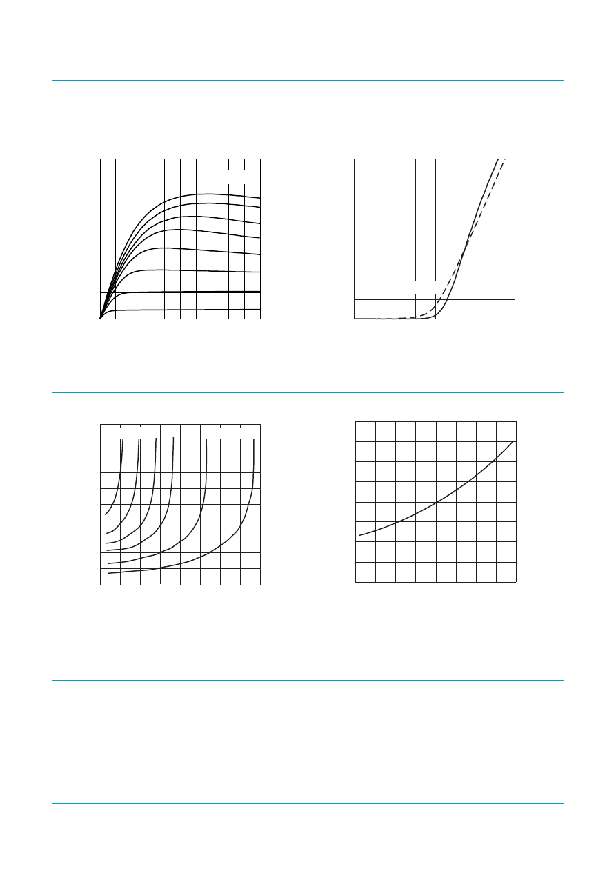
T
j
= 25
°
C
T
j
= 25
°
C and 150
°
C; V
DS
>
I
D
x R
DSon
Fig 5.
Output characteristics: drain current as a
function of drain-source voltage; typical values.
Fig 6.
Transfer characteristics: drain current as a
function of gate-source voltage; typical values.
T
j
= 25
°
C
Fig 7.
Drain-source on-state resistance as a function
of drain current; typical values.
Fig 8.
Normalized drain-source on-state resistance
factor as a function of junction temperature.
003aaa315
0
10
20
30
0
2
4
6
8
10
VDS (V)
ID
(A)
VGS (V) =
16
12
10
9
8
7
6
5
003aaa319
0
2
4
6
8
0
2
4
6
8
VGS (V)
ID
(A)
Tj = 150
°
C
Tj = 25
°
C
003aaa317
100
150
200
250
300
350
0
5
10
15
20
ID (A)
RDSon
(m
Ω
)
VGS (V) = 10
5.5
6
6.5
7
8
03aa28
0
0.6
1.2
1.8
2.4
-60
0
60
120
180
a
Tj (
°
C)
a
R
DSon
R
DSon 25 C
°
(
)
-----------------------------
=
Philips Semiconductors
PHT6N06T
TrenchMOS™ standard level FET
Product data
Rev. 02 — 03 February 2003
7 of 12
9397 750 10633
© Koninklijke Philips Electronics N.V. 2003. All rights reserved.
I
D
= 1 mA; V
DS
= V
GS
T
j
= 25
°
C; V
DS
= 5 V
Fig 9.
Gate-source threshold voltage as a function of
junction temperature.
Fig 10. Sub-threshold drain current as a function of
gate-source voltage.
V
GS
= 0 V; f = 1 MHz
Fig 11. Input, output and reverse transfer capacitances as a function of drain-source voltage; typical values.
03aa32
0
1
2
3
4
5
-60
0
60
120
180
Tj (
°
C)
VGS(th)
(V)
max
min
typ
03aa35
10-6
10-5
10-4
10-3
10-2
10-1
0
2
4
6
VGS (V)
ID
(A)
max
typ
min
003aaa318
10
102
103
10-1
1
10
102
VDS (V)
C
(pF)
Ciss
Coss
Crss
Philips Semiconductors
PHT6N06T
TrenchMOS™ standard level FET
Product data
Rev. 02 — 03 February 2003
8 of 12
9397 750 10633
© Koninklijke Philips Electronics N.V. 2003. All rights reserved.
T
j
= 25
°
C and 150
°
C; V
GS
= 0 V
I
D
= 5 A; V
DD
= 44 V
Fig 12. Source (diode forward) current as a function of
source-drain (diode forward) voltage; typical
values.
Fig 13. Gate-source voltage as a function of gate
charge; typical values.
003aaa320
0
10
20
30
40
VSD (V)
IS
3
2
1
0
(A)
Tj = 150
°
C
Tj = 25
°
C
003aaa331
0
2
4
6
8
10
0
2
4
6
QG (nC)
VGS
(V)
Philips Semiconductors
PHT6N06T
TrenchMOS™ standard level FET
Product data
Rev. 02 — 03 February 2003
9 of 12
9397 750 10633
© Koninklijke Philips Electronics N.V. 2003. All rights reserved.
6.
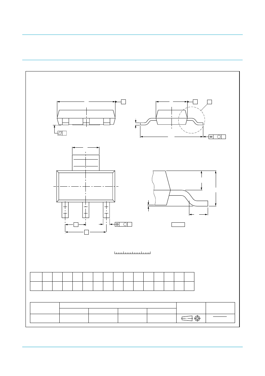
Package outline
Fig 14. SOT223.
UNIT
A
1
b
p
c
D
E
e
1
H
E
L
p
Q
y
w
v
REFERENCES
OUTLINE
VERSION
EUROPEAN
PROJECTION
ISSUE DATE
IEC
JEDEC
EIAJ
mm
0.10
0.01
1.8
1.5
0.80
0.60
b
1
3.1
2.9
0.32
0.22
6.7
6.3
3.7
3.3
2.3
e
4.6
7.3
6.7
1.1
0.7
0.95
0.85
0.1
0.1
0.2
DIMENSIONS (mm are the original dimensions)
SOT223
SC-73
97-02-28
99-09-13
w
M
b
p
D
b
1
e
1
e
A
A
1
L
p
Q
detail X
H
E
E
v
M
A
A
B
B
c
y
0
2
4 mm
scale
A
X
1
3
2
4
Plastic surface mounted package; collector pad for good heat transfer; 4 leads
SOT223

Philips Semiconductors
PHT6N06T
TrenchMOS™ standard level FET
Product data
Rev. 02 — 03 February 2003
10 of 12
9397 750 10633
© Koninklijke Philips Electronics N.V. 2003. All rights reserved.
7.
Revision history
Table 5:
Revision history
Rev Date
CPCN
Description
02
20030203
200209006 Product data (9397 750 10633); supersedes product specification PHT6N06T
Rev 1.000 of September 1997
Modifications:
•
The format of this specification has been redesigned to comply with Philips
Semiconductors new presentation and information standard
•
ESD diodes removed from device and specification
•
Characteristics updated in
.

9397 750 10633
Philips Semiconductors
PHT6N06T
TrenchMOS™ standard level FET
© Koninklijke Philips Electronics N.V. 2003. All rights reserved.
Product data
Rev. 02 — 03 February 2003
11 of 12
9397 750 10633
Philips Semiconductors
PHT6N06T
TrenchMOS™ standard level FET
© Koninklijke Philips Electronics N.V. 2003. All rights reserved.
Product data
Rev. 02 — 03 February 2003
11 of 12
Contact information
For additional information, please visit http://www.semiconductors.philips.com.
For sales office addresses, send e-mail to: sales.addresses@www.semiconductors.philips.com.
Fax: +31 40 27 24825
8.
Data sheet status
[1]
Please consult the most recently issued data sheet before initiating or completing a design.
[2]
The product status of the device(s) described in this data sheet may have changed since this data sheet was published. The latest information is available on the Internet at
URL http://www.semiconductors.philips.com.
[3]
For data sheets describing multiple type numbers, the highest-level product status determines the data sheet status.
9.
Definitions
Short-form specification — The data in a short-form specification is
extracted from a full data sheet with the same type number and title. For
detailed information see the relevant data sheet or data handbook.
Limiting values definition — Limiting values given are in accordance with
the Absolute Maximum Rating System (IEC 60134). Stress above one or
more of the limiting values may cause permanent damage to the device.
These are stress ratings only and operation of the device at these or at any
other conditions above those given in the Characteristics sections of the
specification is not implied. Exposure to limiting values for extended periods
may affect device reliability.
Application information — Applications that are described herein for any
of these products are for illustrative purposes only. Philips Semiconductors
make no representation or warranty that such applications will be suitable for
the specified use without further testing or modification.
10. Disclaimers
Life support — These products are not designed for use in life support
appliances, devices, or systems where malfunction of these products can
reasonably be expected to result in personal injury. Philips Semiconductors
customers using or selling these products for use in such applications do so
at their own risk and agree to fully indemnify Philips Semiconductors for any
damages resulting from such application.
Right to make changes — Philips Semiconductors reserves the right to
make changes in the products - including circuits, standard cells, and/or
software - described or contained herein in order to improve design and/or
performance. When the product is in full production (status ‘Production’),
relevant changes will be communicated via a Customer Product/Process
Change Notification (CPCN). Philips Semiconductors assumes no
responsibility or liability for the use of any of these products, conveys no
licence or title under any patent, copyright, or mask work right to these
products, and makes no representations or warranties that these products are
free from patent, copyright, or mask work right infringement, unless otherwise
specified.
11. Trademarks
TrenchMOS — is a trademark of Koninklijke Philips Electronics N.V.
Level
Data sheet status
Product status
Definition
I
Objective data
Development
This data sheet contains data from the objective specification for product development. Philips
Semiconductors reserves the right to change the specification in any manner without notice.
II
Preliminary data
Qualification
This data sheet contains data from the preliminary specification. Supplementary data will be published
at a later date. Philips Semiconductors reserves the right to change the specification without notice, in
order to improve the design and supply the best possible product.
III
Product data
Production
This data sheet contains data from the product specification. Philips Semiconductors reserves the
right to make changes at any time in order to improve the design, manufacturing and supply. Relevant
changes will be communicated via a Customer Product/Process Change Notification (CPCN).

© Koninklijke Philips Electronics N.V. 2003.
Printed in The Netherlands
All rights are reserved. Reproduction in whole or in part is prohibited without the prior
written consent of the copyright owner.
The information presented in this document does not form part of any quotation or
contract, is believed to be accurate and reliable and may be changed without notice. No
liability will be accepted by the publisher for any consequence of its use. Publication
thereof does not convey nor imply any license under patent- or other industrial or
intellectual property rights.
Date of release: 03 February 2003
Document order number: 9397 750 10633
Contents
Philips Semiconductors
PHT6N06T
TrenchMOS™ standard level FET
Product profile . . . . . . . . . . . . . . . . . . . . . . . . . . 1
Description . . . . . . . . . . . . . . . . . . . . . . . . . . . . 1
Features . . . . . . . . . . . . . . . . . . . . . . . . . . . . . . 1
Applications . . . . . . . . . . . . . . . . . . . . . . . . . . . 1
Quick reference data. . . . . . . . . . . . . . . . . . . . . 1
Pinning information . . . . . . . . . . . . . . . . . . . . . . 1
Limiting values. . . . . . . . . . . . . . . . . . . . . . . . . . 2
Thermal characteristics. . . . . . . . . . . . . . . . . . . 4
Transient thermal impedance . . . . . . . . . . . . . . 4
Characteristics . . . . . . . . . . . . . . . . . . . . . . . . . . 5
Package outline . . . . . . . . . . . . . . . . . . . . . . . . . 9
Revision history . . . . . . . . . . . . . . . . . . . . . . . . 10
Data sheet status . . . . . . . . . . . . . . . . . . . . . . . 11
Definitions . . . . . . . . . . . . . . . . . . . . . . . . . . . . 11
Disclaimers . . . . . . . . . . . . . . . . . . . . . . . . . . . . 11
Trademarks. . . . . . . . . . . . . . . . . . . . . . . . . . . . 11

Mouser Electronics
Authorized Distributor
Click to View Pricing, Inventory, Delivery & Lifecycle Information:
:
Document Outline
- 1. Product profile
- 2. Pinning information
- 3. Limiting values
- 4. Thermal characteristics
- 5. Characteristics
- 6. Package outline
- 7. Revision history
- 8. Data sheet status
- 9. Definitions
- 10. Disclaimers
- 11. Trademarks
Wyszukiwarka
Podobne podstrony:
5N60C 600V 4A Nch mosfet id 430 Nieznany
50w mosfet 540
Mosfet
Badanie tranzystorów unipolarnych typu JFET i MOSFET
tranzystory mosfet(1), Architektura systemów komputerowych, Sentenza, Sentenza
irf7342 HEXFET Power MOSFET
CNC na MOSFet
2663 HybrydowyWzmLampowo MOSFET
Sprawozdanie MOSFET PiotrowskiTomasz
mosfet400W, Protel Schematic
MOSFET
Introduction to the MOSFET and MOSFET Inverter(1)
irf7103 HEXFET Power MOSFET id 220258
Badanie tranzystorow polowych MOSFET cw6
Cw 06 Tranzystor MOSFET id 1213 Nieznany
energoelektronika sciaga -falownik-zasilacz-MOSFET-IGBT-klucz tranz, Politechnika Lubelska, Studia,
Ir2111 High Voltage High Speed Power Mosfet And Igbt Driver
A Class A MOSFET Headphone Driver
więcej podobnych podstron