© Freescale Semiconductor, Inc., 2004. All rights reserved.
Freescale Semiconductor
In the pursuit of raw computing
horsepower, designers often try to
improve throughput of designs through an increase in CPU clock
frequency. But at a certain point, bus bandwidth and access speed
to main memory become the limiting factors in overall processor
throughput. This limitation may be overcome with faster, more
expensive memory. However, at some point economic feasibility
becomes an issue. A good cache memory design and
implementation can help to minimize bus latency and improve
overall processor throughput, all with modest economic cost.
1
What is a Cache?
A cache is commonly defined as a secure place of storage, mainly
for preserving provisions or implements. A cache, as it applies to
computing, is a small block of high speed memory, employed to
make a CPU with a large amount of slow, inexpensive memory
think it has immediate, and very fast, access to that large bank of
slow memory. The goal of a cache in computing is to keep the
expensive CPU as busy as possible by minimizing the wait for
reads and writes to slower memory.
To help explain a cache, here is a simple example of a cook
working in a restaurant kitchen. To maintain the ultimate in
freshness, every time an order comes into the kitchen, the cook
runs out to the supermarket across the street and buys all the
ingredients needed to fill the order. This is time consuming, and as
business grows, it starts to limit the total number of orders he can
cook during a given mealtime; besides, customers become
AN2663
Rev. 1, 10/2004
Contents
1. What is a Cache? . . . . . . . . . . . . . . . . . . . . . . . . . . . . . . 1
2. Associativity . . . . . . . . . . . . . . . . . . . . . . . . . . . . . . . . . 2
3. Writes to Cache . . . . . . . . . . . . . . . . . . . . . . . . . . . . . . . 5
4. Multi-Level Caches . . . . . . . . . . . . . . . . . . . . . . . . . . . . 6
5. Frontside versus Backside Cache . . . . . . . . . . . . . . . . 10
6. Example Cache Implementation: PowerQUICC III™ 10
7. References . . . . . . . . . . . . . . . . . . . . . . . . . . . . . . . . . . 15
A Cache Primer
by
Paul Genua, P.E.
Freescale Semiconductor, Inc.
Austin, TX

A Cache Primer, Rev. 1
2
Freescale Semiconductor
Associativity
agitated at the time it takes to prepare the food. The cook, being a smart man, sits down one night and analyzes all
the orders for the previous week. He notices a trend—that there is a great amount of commonality in the ingredients
in all orders. He buys a refrigerator to store the most commonly used items, and saves himself some trips to the
supermarket. To increase his efficiency further, he organizes his products on the shelves of the refrigerator and
creates a list of the items on hand and posts it on the refrigerator door. Now when an order comes in, he checks the
list to see if he has the necessary ingredients on hand, and if not he can run across the street.
This is the concept behind cache. In this example, the cook is the expensive resource, the CPU, the supermarket is
the large amount of RAM in a system, the cache is the refrigerator, and the list is the cache directory.
The cook and restaurant example is somewhat simplified. For example, what happens when the refrigerator gets full.
The cook might throw away the oldest ingredient in the refrigerator, or possibly the ingredient that has the nearest
expiration date. Disposing items based on freshness or expiration date is analogous to a cache’s replacement
algorithm.
2
Associativity
A cache is essentially a small, but fast, memory that is separate from a processor’s main memory. A cache’s
associativity determines how main memory locations map into cache memory locations. A cache is said to be fully
associative if its architecture allows any main memory location to map into any location in the cache. In a fully
associative cache, a directory shows the mappings of main memory to cache memory locations. A directory location
is then assigned whenever something is put in cache. Problems arise with full associativity when searching through
the cache array for an entry. With a large cache, scanning the directory can be time consuming and usually requires
either a great many expensive CPU cycles, or additional hardware support such as a content addressable memory
(CAM). Unfortunately large CAMs are expensive, so other methods for traversing through a cache were developed.
Associativity is a little difficult to imagine in the cook and refrigerator example, so here is a more numerical
example. Imagine, for example, an SDRAM based memory system that has addresses from 0x0000–0xFFFF.
Furthermore, assume that the 4 most significant address bits describe a row, and the last 12 bits describe columns
within a row. A cache can be imagined with enough room to hold 0xFFF entries, which accounts for all columns.
An SDRAM address can then be stored in the cache based on its column address. For example, address 0xABCD
would be stored at cache address 0xBCD. The directory would still contain all 0xFFF entries in the cache, however
each entry would be at the location in the directory matching the column address, so only the row address would
actually need to be written in the directory. Since the SDRAM is 16 times larger than the cache, 16 SDRAM address
would map to each cache entry. In the above example, for an access to address 0xABCD, a 0xA is written to the
directory entry for 0xBCD and the actual data to be cached would be stored at location 0xBCD. This takes away the
decision on where to store the new cache entry. This is called a set-associative architecture.
A Cache Primer, Rev. 1
Freescale Semiconductor
3
Associativity
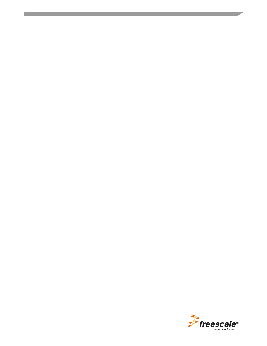
Figure 1. Set-Associative Example
With a set-associative architecture there is no need for a big CAM or cross reference to determine which cache
location contains which addresses; the directory address is based on the main memory address. In
the
column address is the cache’s set address. Within any set, the entry is associative and can have any row address.
These row addresses are referred to as the tag bits.
It seems that a set-associative cache would provide a less flexible cache design; what would drive someone to use a
set-associative cache over a fully associative cache? The quick answer is speed. Each access to a fully associative
cache must begin with the processor scanning a directory for the address matching the associated memory. A
set-associative cache reduces this latency dramatically. For a read cycle, in the above example the lower 12 bits of
address are routed to both the cache and the RAM. While the cache finds the entry based on these lower bits, the
column address in this case, the directory looks at the upper 4 bits to tell if there is a match. Cache address 0xBCD
is accessed and ready to go, waiting for the directory to tell the CPU if there is a match between the stored tag, 0xA,
or whether there is some other address tag in that slot. In this case, the data can be made available while the tag match
is being made. In a fully associative cache, a complete match must be made before data can be accessed.
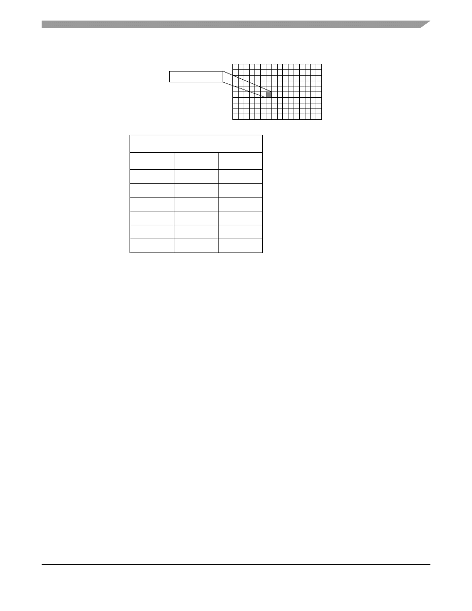
A greater degree of associativity, or more ways in the cache, improves hit rates within a cache. Each way is a copy
of the cache, with its own set RAM and its own tag RAM. An n-way set-associative cache will have n set RAM’s
and n tag RAM’s. In
the set 0xBCD has two different valid tags, corresponding to address 0xABCD and
0xDBCD.
0xABCD
Directory
Valid
Tag
Set
1
0x2
0xBCA
0
0xBCB
1
0x0
0xBCC
1
0xA
0xBCD
1
0xC
0xBCE
0
0xBCF
A Cache Primer, Rev. 1
4
Freescale Semiconductor
Associativity
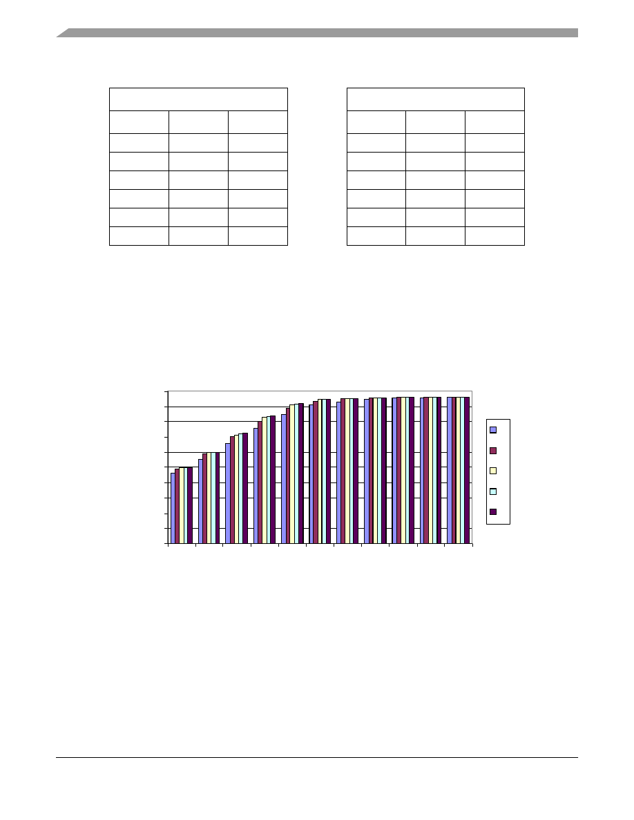
A cache’s hit rate increases with more ways.
demonstrates that beyond a certain point, increasing cache size
has more of an impact than increasing associativity.
NOTE
The data for
and
was obtained through a cache simulator while
simulating the GCC compiler. Associativity was varied, as well as cache size.
Figure 2. Varying Associativity over Cache Size
Table 1. Two Way Set-Associative Cache
Way 1
Way 2
Valid
Tag
Set
Valid
Tag
Set
1
0xA
0xBCA
1
0x2
0xBCA
0
0xBCB
0
0xBCB
0
0xBCC
1
0x0
0xBCC
1
0xD
0xBCD
1
0xA
0xBCD
0
0xBCE
1
0xC
0xBCE
1
0x2
0xBCF
0
0xBCF
0
10
20
30
40
50
60
70
80
90
100
1k
2k
4k
8k
16k
32k
64k
128k 256k 512k
1M
Cache Size
Hi
t Ra
te
1
2
4
8
16
A Cache Primer, Rev. 1
Freescale Semiconductor
5
Writes to Cache
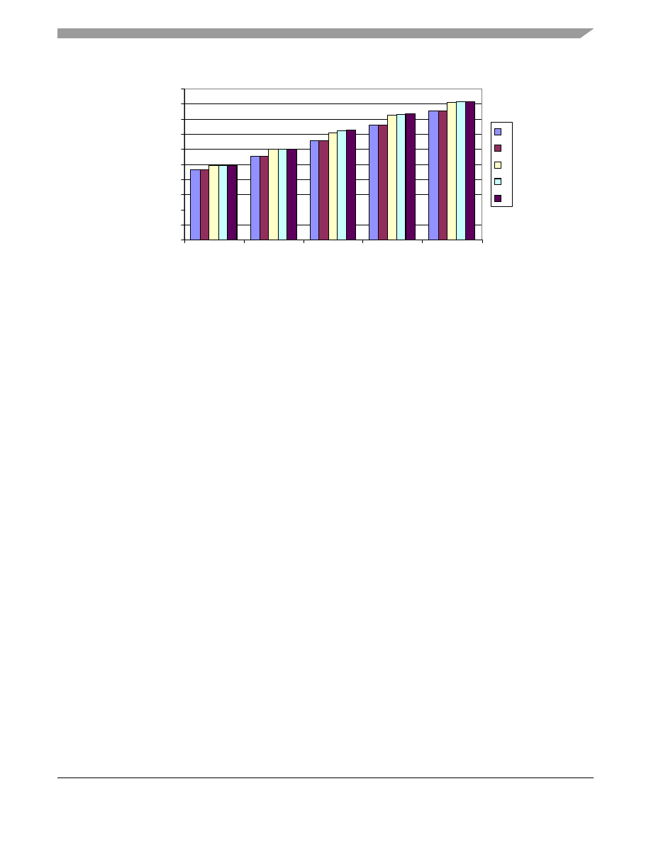
Figure 3. Zooming in on Associativity versus Cache Size
With a 4-Kbytes cache size, the difference between 3- and 5-way set associativity is miniscule compared to doubling
the cache size. The complexity of the cache increases in proportion to the associativity, and in this case, would not
be justifiable against increasing cache size to 8 or even 16 Kbytes.
3
Writes to Cache
Coherency and speed are chief concerns with writes in cache architecture. Coherency is the consistency of data
between cache and memory. This is more important in multi-processor systems with shared memory, or in systems
where integrated peripherals on a CPU core all share memory. Because reads dominate processor accesses, caches
are usually optimized to speed up read accesses. For example, all instruction fetches are read accesses, and most
instructions do not write to memory.
There are two cache designs used for writes:
•
Write Through—writes to both the cache and the memory
on every write access, regardless of a cache
hit or miss. The writes to main memory ensure coherency but slow the speed of the processor by
accessing RAM for every write.
•
Copy Back—writes data only to the cache. This cache design writes data only to memory when the cache
block is replaced or when another device needs access to this block of memory.
Data writes to RAM once
the cache block is replaced, reducing main memory accesses. The major advantage of a copy back
cache is speed. Write cycles become much faster than if main memory had to be written to for every
write. In addition, the processor is on the memory bus much less of the time, which becomes a great
advantage in multiprocessor systems sharing a main memory bus.
For all of its advantages, copy-back caches require more complexity in tracking data written to cache but not to main
memory. The modified bit, or dirty bit, is one method devised for memory housekeeping purposes. In such a method,
an extra bit is used for each cache entry. Data that has been written to the cache, but not to main memory, is
considered modified and is tagged as such by this extra bit. During a cache miss, or if the cache entry is about to be
replaced, the dirty bit is checked to see if data first must be written to memory.
Although implementing a dirty bit is a simple way to maintain coherency, the increased complexity increases access
latency.
0
10
20
30
40
50
60
70
80
90
100
1k
2k
4k
8k
16k
Cache Size
H
it R
a
te
1
2
3
4
5
A Cache Primer, Rev. 1
6
Freescale Semiconductor
Multi-Level Caches
4
Multi-Level Caches
Cache design is a cost/performance trade off. Processor designers confront design decisions of cost of wafer space
and eventual die size, versus on-chip cache size. Board designers confront the cost of high speed memory. The
typical board designer uses huge blocks of inexpensive SDRAM for instruction and program storage. Therefore to
minimize the access time of the main memory during processor cache misses, the designer can use some tricks such
as interleaving SDRAM memory. Interleaving involves keeping multiple SDRAM pages open at one time,
minimizing precharge commands and speeding accesses to open SDRAM pages. But there is inherent complexity
in keeping multiple pages open and performance degrades significantly with accesses to closed pages. Eliminating
precharges on a handful of SDRAM pages can only speed things up so much. Even greater performance can be
achieved by building an off-chip cache of faster memory outside the processor, an L2 (Level 2) cache, to accelerate
the access time of SDRAM during on-chip misses.
Other than saving die space, a multi-level caching scheme is advantageous when examined with a cost/performance
mindset. Typically a processor designer must choose between a small, fast cache and a large, slow one. The larger
the RAM, the more logic required for its address decodes, and the longer the critical path, increasing latency. Large
RAM arrays tend to be slower than small ones. Processor design typically results in a small fast cache followed by
a larger (but slower) downstream cache. Even within a single processor core, two levels of on-chip cache are not
necessarily of the same speed.
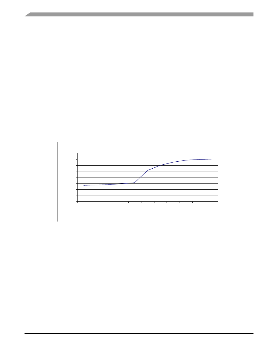
Figure 4. 16 Kbyte L1 versus L2
In the two-level cache system simulation shown in
the 16 Kbyte L1 cache exhibits a 92% hit rate, meaning
that 8% of total traffic gets to the secondary cache. By adding a secondary cache that is four times larger than the
L1, the total hit rate improves to 95%. The total miss rate is now 5%, or only 3% better, which means that the
secondary cache has a hit rate of about 38%. At first glance, the 3% improvement with a multi-level cache seems
insignificant, but miss rate drops from 8% in a single-level system to 5% in the two-level system, or roughly by 40%.
This means that bus traffic in the two-level system is about 40% less than that of in the single-level system, which
is significant in a multiprocessing architecture where more than one resource shares the bus.
The hit rates for the above example are fictitious data. Actual hit rate is a factor of the cache hardware, as well as
the compiler and the end code.
Section 4.1, “L1 and L2 Simulations,”
shows examples of cache simulations and their
resultant hit rates.
It is easy to see the benefits of a multi-level cache in eliminating main memory traffic. In the world of
cost/performance trade-offs and slow inexpensive main memory, minimizing main memory accesses through a fast
multi-level cache provides increased performance to the CPU, sometimes even greater than raw clock cycles.
89
90
91
92
93
94
95
96
97
1k
2k
4k
8k
16k
32k
64k
128k 256k 512k
1M
L2 Size
Hit
Ra
te
A Cache Primer, Rev. 1
Freescale Semiconductor
7
Multi-Level Caches
4.1
L1 and L2 Simulations
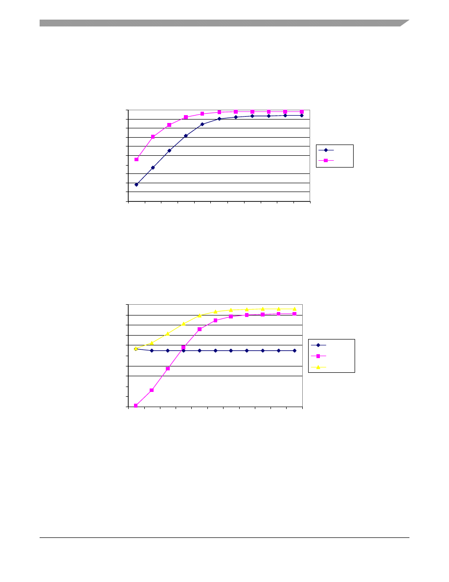
shows simulated values for cache hits running two popular algorithms, the Spice electronics simulator, and
the GCC compiler. Cache hit ratios takes the shape of an elongated S curve, asymptotically approaching a point at
which doubling cache size makes little impact on the total number of hits to the cache.
Figure 5. L1 Cache Hits
shows L2 hit rates for a fixed 1 Kbyte L1 cache size while running the GCC compiler. Notice again that
the L2 hit rate takes the form of an elongated S curve. In the example below, once the L2 cache size reaches about
32 Kbytes, it no longer makes a significant impact on the total hit rate.
Figure 6. Hit Rates for Increasing L2 Cache Size, with 1 Kbyte L1
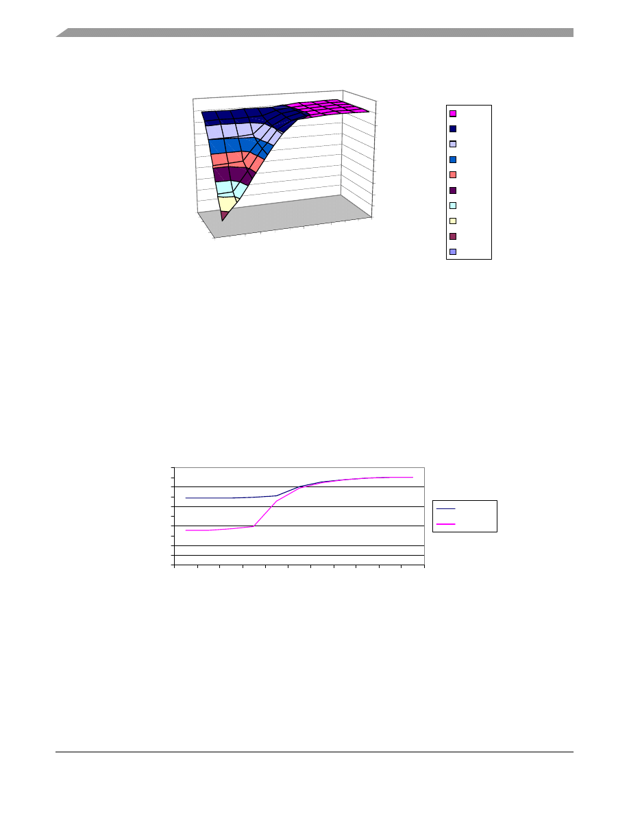
shows a three-dimensional view of cache hits while changing both L1 and L2 cache size. Again, this
algorithm peaks out at just under 96% cache hits. This is due to the nature of the specific algorithm being simulated.
It is interesting to see that a 16 Kbyte L1 with a 1 Kbyte L2 gives almost the same results (91% hits) as a 1 Kbyte
L1 with an L2 of 16 Kbytes (89% hits).
80
82
84
86
88
90
92
94
96
98
100
1
2
4
8
16
32
64
12
8
25
6
51
2
10
24
Cache Size in Kbytes
Hit
Ra
te
CC
Spice
0
10
20
30
40
50
60
70
80
90
100
1
2
4
8
16
32
64
12
8
25
6
51
2
10
24
Cache Size in Kbytes
Hi
t Ra
te
L1 Hit
L2 Hit
Total Hit
A Cache Primer, Rev. 1
8
Freescale Semiconductor
Multi-Level Caches
Figure 7. Hit Rates for Changing L1 and L2 Size
Perhaps the most educating aspect of this exercise is in noticing the impact of L2 to total hits with respect to L1 size.
L2 has little effect on the total number of cache hits until it is at least double the L1 cache size. As seen in
,
the steepest part of the slope for an L1 cache of 8 Kbytes, is for an L2 cache of 16 Kbytes. Again for an L1 cache of
16 Kbytes, the steepest part of the curve is for an L2 cache size of 32 Kbytes. Prior to that point, the L2 cache has
little, if any, impact on total cache performance. Since the L2 cache has the same line size as the L1 cache, the only
hits on the downstream cache are from L1 cache misses caused by conflicts in the L1. The L2 cache is essentially
filled with the same data as the L1 cache, at the time it is loaded into the L1 cache. The only way that this data can
stay in the L2 cache, but be removed from the L1 cache, is if the primary cache has a conflict that necessitates
rewriting its copy of the cache line. To ensure that the same conflict does not rewrite the L2 cache, the L2 cache
needs to be considerably larger, either containing a larger address space or a larger line size.
Figure 8. Total Hits (L1 and L2) for 8 Kbyte and 16 Kbyte L1
It is important to remember that these graphs are the result of a simulation, and not actual measured data. The
simulation has a flaw in that it allows the cache enormous spatial locality within the code. On a real system, a
processor would most likely be running an Operating System, and handling more than one task at a time. Upon each
task switch from one thread to another, locations in cache would be flushed and then re-issued to new memory
locations corresponding to the new thread. In addition the OS, would be running and would most likely use some
1k
4k
16k
64
k
25
6k
1M
1k
16k
50
55
60
65
70
75
80
85
90
95
100
Hit Rate
L2 Size
L1 Size
95-100
90-95
85-90
80-85
75-80
70-75
65-70
60-65
55-60
50-55
78
80
82
84
86
88
90
92
94
96
98
1k
2k
4k
8k
16
k
32
k
64
k
12
8k
25
6k
51
2k
1M
L2 Size
Hi
t Ra
te
L1 = 16k
L1 = 8k
A Cache Primer, Rev. 1
Freescale Semiconductor
9
Multi-Level Caches
space in cache. In the above examples, both the GCC compiler and Spice only occupied a few Kbytes of code space
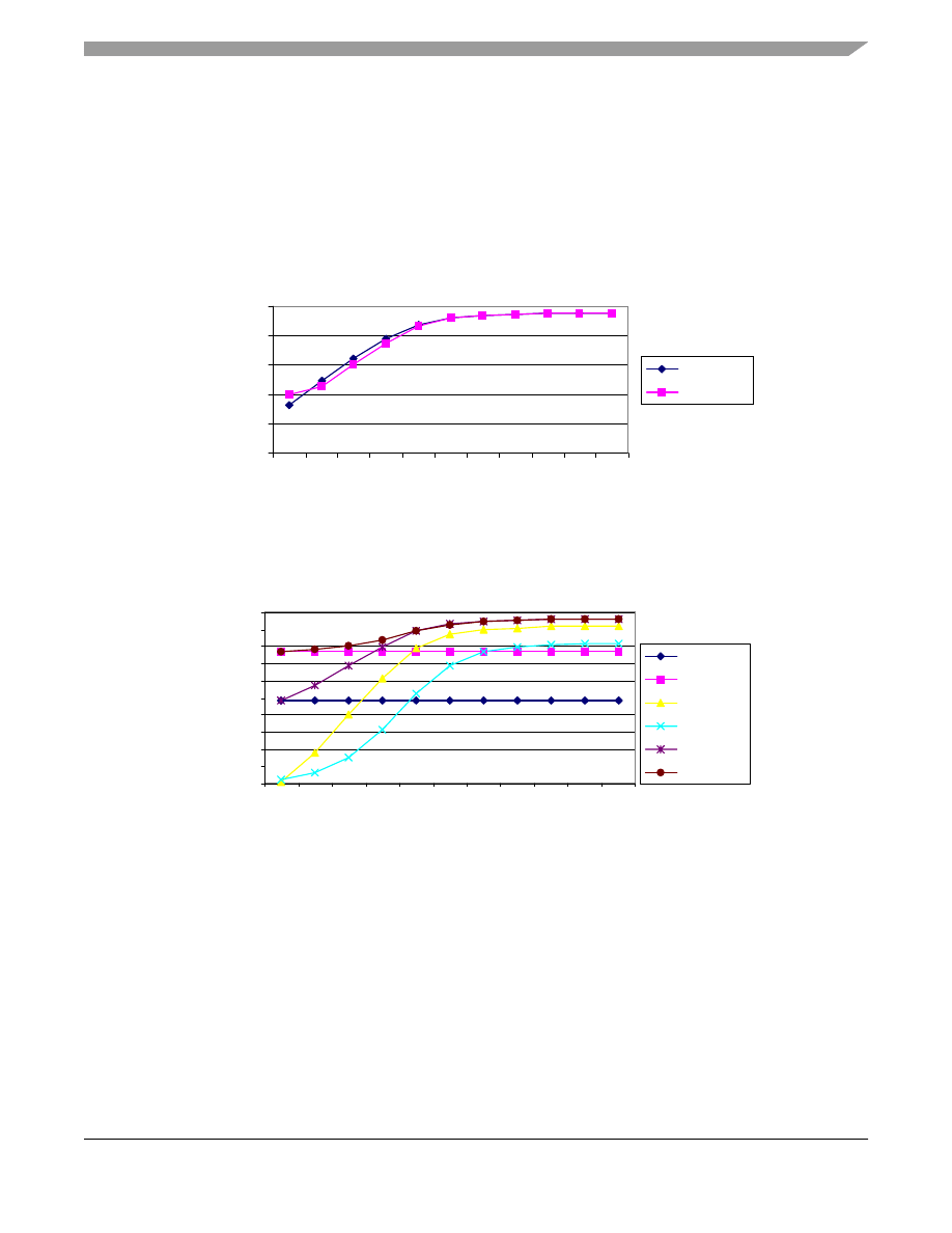
each. When cache size reaches about 16 Kbytes, the whole instruction space seems to fit within cache. 100% of
instruction hits is never achieved, mainly because associativity was kept at two. The code spans multiple Kbytes and
thus has overlapping set addresses.
shows the split between instruction and data hits for an associativity of
2. Notice that instruction and data hits both taper off at just under 100%. Increasing the instruction cache size from
64 Kbytes to 1 Mbyte makes little difference in performance. Increasing associativity to 4 from 2 increases the hit
rate from a maximum of 98.6% to 98.8% (not shown). Other factors such as block size and replacement algorithm
can also help in achieving higher hit rates.
Figure 9. Instruction versus Data Hits for L1 Cache
Figure 10. L2 Instruction versus Data Cache Hits (Varying L2 size)
NOTE
The previous figures were all created on a cache simulator while simulating the
GCC compiler. The L1 cache is configured as two 2-way set-associative
independent caches (instruction and data), with block size of 4. The L2 cache is
configured as a unified cache, block size of 4, 2-way set-associative.
75
80
85
90
95
100
1
2
4
8
16
32
64
12
8
25
6
51
2
10
24
Cache Size in Kbytes
Hi
t Ra
te
Instruction
Data
0
10
20
30
40
50
60
70
80
90
100
1
2
4
8
16
32
64
128
256
512 1024
Cache Size in Kbytes
Hit
Ra
te
L1 Inst
L1 Data
L2 Inst
L2 Data
Total Inst
Total Data
A Cache Primer, Rev. 1
10
Freescale Semiconductor
Frontside versus Backside Cache
5
Frontside versus Backside Cache
When designing cache between the core and the memory subsystem, there is a trade off in its placement and two
different architectures have emerged.
A frontside cache is implemented inline with the memory system as modeled in
Figure 11. Frontside Cache
This configuration is so named because of the cache’s situation on the frontside bus, or memory bus, of the
microprocessor. Typically, the frontside bus runs at a fraction of the processor speed. For instance, on the
PowerQUICC II™ processor it is likely that the processor core runs at 200 MHz, while using only a 66 MHz bus
speed. The frontside cache, also runs at the frontside speed of 66 MHz.
In comparison, a backside cache is typically implemented through a dedicated bus, separate from the main memory
bus as configured in
.
Figure 12. Backside Cache
Because it is on a dedicated bus, a backside cache is typically clocked faster than the main system (frontside) bus.
With for example, Freescale’s MPC7410 microprocessor, it is possible to run the core at 400 MHz, with a 133 MHz
frontside bus, and a 400 MHz backside bus. This means that the off-chip L2 cache can run at the full core rate of
400 MHz.
6
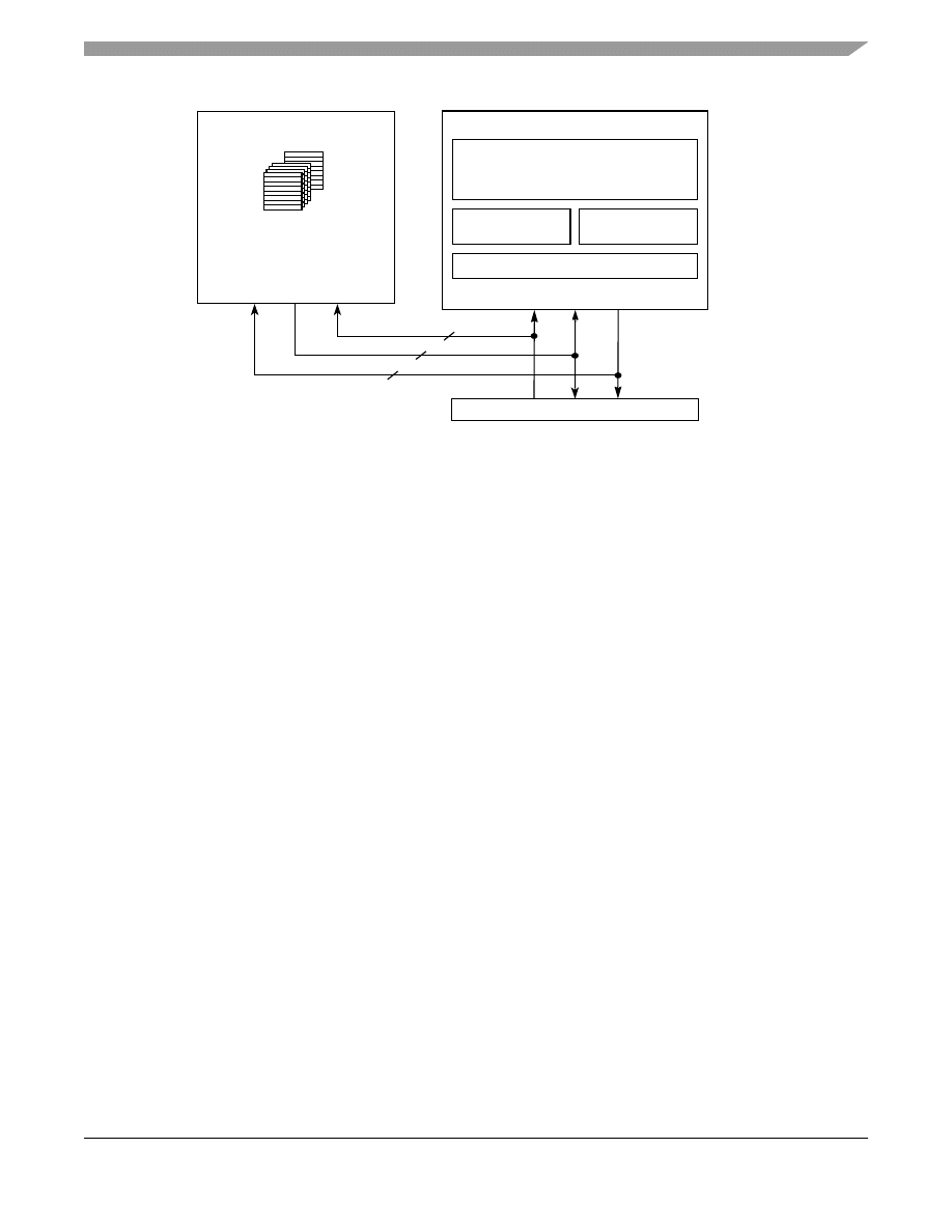
Example Cache Implementation: PowerQUICC III™
At the heart of the PowerQUICC III is the e500 core, containing separate data and instruction caches, which are
32-Kbyte, eight-way set-associative L1 caches. In addition, the PowerQUICC III is the first processor in Freescale’s
PowerQUICC family of processors to incorporate an on-chip L2 cache.
shows a diagram of the e500 core
and caches.
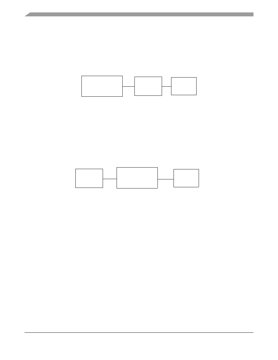
Cache
Processor
RAM
Cache
Processor
RAM
A Cache Primer, Rev. 1
Freescale Semiconductor
11
Example Cache Implementation: PowerQUICC III™
Figure 13. e500 Core and Caches
6.1
L1 Caches
The e500 core features an integrated L1 cache, designed as a Harvard architecture so as to have a separate L1 data
and instruction cache. Each L1 cache is 32-Kbyte and eight-way set associative.
The following are some features of both the L1 data and instruction caches:
•
32-Kbyte size
•
Eight-way set associative
•
Pseudo least recently used (PLRU) replacement policy
•
Cache block size is 32 bytes (8 words)
•
Individual line locking
•
Parity generation and checking
e500 Core
32-Kbyte L1
Instruction Cache
32-Kbyte L1
Data Cache
Core Complex Bus
e500 Core Complex
128-Kbyte
L2 Cache/SRAM
Coherency Module
64 bit input
128 bit input
128 bit output
128-Kbyte bank
(8-way)
programmable
as L2 cache or SRAM
WR
RD2
RD1
DOUT
WR IN
RD IN
A Cache Primer, Rev. 1
12
Freescale Semiconductor
Example Cache Implementation: PowerQUICC III™
shows the basic L1 cache organization.
Figure 14. L1 Cache Organization
Note: The status bits are different in the data and instruction caches.The data cache supports three-state MEI memory
coherency protocols with 3-bit status and 1-bit coherency valid fields. The instruction cache has only a 1-bit coherency valid field
and eight instructions in a block.
Each block of data cache consists of 32 bytes of data, three status bits, one lock bit, and an address tag. The data
cache supports three-state MEI coherency. For the L1 data cache, a cache block is a 32-byte cache line containing 8
contiguous words from memory. Data cache has one parity bit per word (not shown in
). Physical address
bits 20–26 provide an index to select a cache set. Tags consist of physical address bits 0–19. Address bits 27–31
locate a byte within the selected block.
Additionally, the data cache supports hit-under-miss conditions. Hit-under-miss is a capability that permits the core
to access the cache while a fill for an earlier miss is pending. Up to four misses can be pending in the load miss
queue.
The instruction cache is organized similarly to the L1 data cache. Each block consists of eight instructions, one status
bit, one lock bit, and an address tag. For the L1 instruction cache, a cache block is a 32-byte cache line containing
8 contiguous words from memory. The instruction cache has one parity bit per word (not shown in
).
Physical address bits 20–26 provide an index to select a cache set. Tags consist of physical address bits 0–19.
The instruction cache also allows for hit-under-miss conditions.
The e500 registers L1CSR0 and L1CSR1 provide for cache configuration and control of the L1 caches as defined
by the Freescale Book E standard. Descriptions of these registers can be found in the MPC8560 PowerQUICC III
Integrated Communications Processor Reference Manual.
In addition, L1CFG0 is a read-only register that allows software to read the status of the L1 cache. Information such
as line size, cache replacement policy, Harvard or unified, are available to enable software to make decisions and
use the cache appropriately. This will become more useful as new derivatives of the e500 core are put into use.
128 Sets
Way 5
Way 6
Way 7
Way 4
Address Tag 4
Address Tag 5
Address Tag 6
Address Tag 7
Way 1
Way 2
Way 3
Way 0
Address Tag 0
Address Tag 1
Address Tag 2
Address Tag 3
Status
Status
Status
Words/Instructions [0–7]
Status
Words/Instructions [0–7]
Words/Instructions [0–7]
Words/Instructions [0–7]
Status
Status
Status
Words/Instructions [0–7]
Status
Words/Instructions [0–7]
Words/Instructions [0–7]
Words/Instructions [0–7]
8 Words/Instructions Block

A Cache Primer, Rev. 1
Freescale Semiconductor
13
Example Cache Implementation: PowerQUICC III™
6.2
L2 Cache
In addition to the L1 caches integrated in the e500 core, the PowerQUICC III provides an on-chip unified L2 cache.
The following are features of the L2 cache:
•
256-Kbyte unified cache can be configured for instructions, data, or both
•
write-through
•
frontside cache
•
Pseudo-least-recently-used (PLRU) replacement policy
•
Data protected by ECC
•
Tags protected by parity
•
Fully Pipelined, nonblocking (allows hits under misses)
•
Individual line locking
The L2 cache resides on the frontside bus of the e500 core. In previous sections of this document, differences
between frontside and backside cache architectures are described. The frontside cache is designed to run at main
memory bus speed. However, the frontside design allows for easy access to the cache from I/O masters such as
gigabit Ethernet, RapidIO, and the CPM. In addition, the frontside design allows the flexibility to share data between
cores in future dual core architectures. The frontside architecture in the PowerQUICC III allows for more
performance with less complexity, thereby lowering die size and in turn, cost and power.
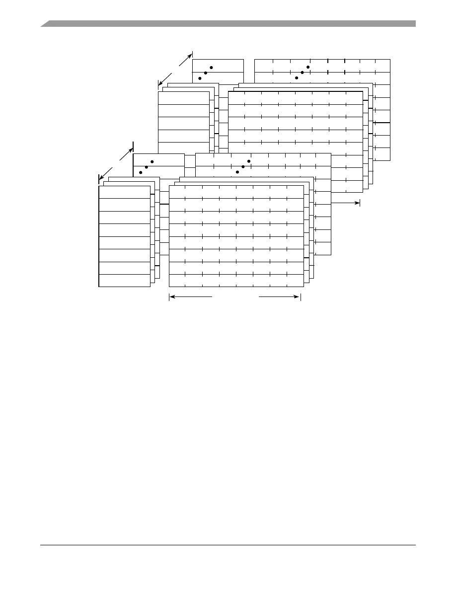
6.2.1 L2 Organization
The PowerQUICC III’s L2 cache is organized as two banks of 512 sets each, both containing eight ways as shown
in
. Each block consists of 32 bytes of data and an address tag.
A Cache Primer, Rev. 1
14
Freescale Semiconductor
Example Cache Implementation: PowerQUICC III™
Figure 15. L2 Cache Organization
In addition, the L2 cache array allows the option of being partitioned into private on-chip SRAM. It can be
partitioned into one 256 Kbyte region, or two 128 Kbyte regions (residing at any aligned location within the memory
map). I/O devices access the SRAM by marking data snoopable (global).
6.3
Buses to the L2 Cache
In
, there are three buses between the PowerQUICC III’s coherency module, L2 cache, and e500 core.
These are described as a 64-bit input bus, a 128-bit input bus, and a 128-bit output bus, and are referred to with
respect to the L2. Keep in mind that the DDR memory bus is 64 bits wide. The 128-bit datapaths were designed to
provide twice the bandwidth of DDR, allowing L2 traffic to be serviced without impacting bandwidth to DDR.
The 128-bit output bus is intended for use with L1 data that is castout to L2 cache or DDR memory. It is also used
for uncached write data to either I/O or DDR memory.
L2 data is provided to the e500 core through the 128-bit input bus upon an L1 miss and L2 hit. In this case, L2 data
is provided to the core critical double-word first. Data is available for execution without waiting for the entire L1
cache line to be reloaded. The 128-bit bus is also used in the case of a read from L2 for I/O snooped responses or an
e500 read of L2 SRAM.
The 64-bit input bus is sized to the DDR bus. It is used in the case of an L2 miss (where data would be allocated to
L1 and L2), an I/O stash to L2, an I/O write to L2 SRAM, or uncached read data to the CPU. Data is supplied
critical-word first. All three buses operate at 333 MHz, the DDR data rate.
512 Sets
Block 5
Block 6
Block 7
Way 4 Address Tag 4
Address Tag 5
Address Tag 6
Address Tag 7
Way 1
Way 2
Way 3
Way 0 Address Tag 0
Address Tag 1
Address Tag 2
Address Tag 3
Words [0–7]
Words [0–7]
Words [0–7]
Words [0–7]
Words [0–7]
Words [0–7]
Words [0–7]
Words [0–7]
8 Words/Block
512 Sets
Way 5
Way 6
Way 7
Way 4 Address Tag 4
Address Tag 5
Address Tag 6
Address Tag 7
Way 1
Way 2
Way 3
Way 0 Address Tag 0
Address Tag 1
Address Tag 2
Address Tag 3
Words [0–7]
Words [0–7]
Words [0–7]
Words [0–7]
Words [0–7]
Words [0–7]
Words [0–7]
Words [0–7]
Bank 1
Bank 0
8 Words/Block
A Cache Primer, Rev. 1
Freescale Semiconductor
15
References
7
References
Handy, Jim, The Cache Memory Book, pp. 8–21, 64–66, 89–94, Academic Press Inc. 1998.
Hennessy, John and David Patterson, Computer Architecture: A Quantitative Approach, pp. 372–441, Morgan
Kaufmann 1995.
MPC8560 PowerQUICC III Integrated Communications Processor Reference Manual (MPC8560RM)
PowerPC™ e500 Core Complex Reference Manua
l
(E500CORERM)
8
Revision History
provides a revision history for this application note.
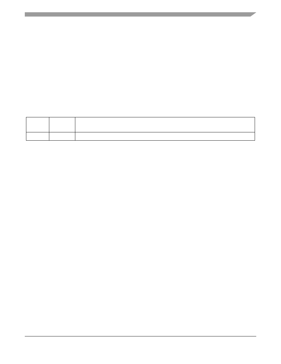
Table 2. Document Revision History
Revision
Number
Date
Substantive Change(s)
1
10/04/2004
Initial release
AN2663
Rev. 1
10/2004
How to Reach Us:
Home Page:
www.freescale.com
email:
support@freescale.com
USA/Europe or Locations Not Listed:
Freescale Semiconductor
Technical Information Center, CH370
1300 N. Alma School Road
Chandler, Arizona 85224
(800) 521-6274
480-768-2130
support@freescale.com
Europe, Middle East, and Africa:
Freescale Halbleiter Deutschland GmbH
Technical Information Center
Schatzbogen 7
81829 Muenchen, Germany
+44 1296 380 456 (English)
+46 8 52200080 (English)
+49 89 92103 559 (German)
+33 1 69 35 48 48 (French)
support@freescale.com
Japan:
Freescale Semiconductor Japan Ltd.
Technical Information Center
3-20-1, Minami-Azabu, Minato-ku
Tokyo 106-0047 Japan
0120 191014
+81 3 3440 3569
support.japan@freescale.com
Asia/Pacific:
Freescale Semiconductor Hong Kong Ltd.
Technical Information Center
2 Dai King Street
Tai Po Industrial Estate,
Tai Po, N.T., Hong Kong
+800 2666 8080
support.asia@freescale.com
For Literature Requests Only:
Freescale Semiconductor
Literature Distribution Center
P.O. Box 5405
Denver, Colorado 80217
(800) 441-2447
303-675-2140
Fax: 303-675-2150
LDCForFreescaleSemiconductor@
hibbertgroup.com
Information in this document is provided solely to enable system and software implementers to
use Freescale Semiconductor products. There are no express or implied copyright licenses
granted hereunder to design or fabricate any integrated circuits or integrated circuits based on the
information in this document.
Freescale Semiconductor reserves the right to make changes without further notice to any
products herein. Freescale Semiconductor makes no warranty, representation or guarantee
regarding the suitability of its products for any particular purpose, nor does Freescale
Semiconductor assume any liability arising out of the application or use of any product or circuit,
and specifically disclaims any and all liability, including without limitation consequential or
incidental damages. “Typical” parameters which may be provided in Freescale Semiconductor
data sheets and/or specifications can and do vary in different applications and actual performance
may vary over time. All operating parameters, including “Typicals” must be validated for each
customer application by customer’s technical experts. Freescale Semiconductor does not convey
any license under its patent rights nor the rights of others. Freescale Semiconductor products are
not designed, intended, or authorized for use as components in systems intended for surgical
implant into the body, or other applications intended to support or sustain life, or for any other
application in which the failure of the Freescale Semiconductor product could create a situation
where personal injury or death may occur. Should Buyer purchase or use Freescale
Semiconductor products for any such unintended or unauthorized application, Buyer shall
indemnify and hold Freescale Semiconductor and its officers, employees, subsidiaries, affiliates,
and distributors harmless against all claims, costs, damages, and expenses, and reasonable
attorney fees arising out of, directly or indirectly, any claim of personal injury or death associated
with such unintended or unauthorized use, even if such claim alleges that Freescale
Semiconductor was negligent regarding the design or manufacture of the part.
Freescale™ and the Freescale logo are trademarks of Freescale Semiconductor, Inc. All other
product or service names are the property of their respective owners.
© Freescale Semiconductor, Inc. 2004.
Document Outline
- A Cache Primer
- 1 What is a Cache?
- 2 Associativity
- 3 Writes to Cache
- 4 Multi-Level Caches
- Figure 4. 16 Kbyte L1 versus L2
- 4.1 L1 and L2 Simulations
- Figure 5. L1 Cache Hits
- Figure 6. Hit Rates for Increasing L2 Cache Size, with 1 Kbyte L1
- Figure 7. Hit Rates for Changing L1 and L2 Size
- Figure 8. Total Hits (L1 and L2) for 8 Kbyte and 16 Kbyte L1
- Figure 9. Instruction versus Data Hits for L1 Cache
- Figure 10. L2 Instruction versus Data Cache Hits (Varying L2 size)
- 5 Frontside versus Backside Cache
- 6 Example Cache Implementation: PowerQUICC III™
- 7 References
- 8 Revision History
Wyszukiwarka
Podobne podstrony:
Abolicja podatkowa id 50334 Nieznany (2)
4 LIDER MENEDZER id 37733 Nieznany (2)
katechezy MB id 233498 Nieznany
metro sciaga id 296943 Nieznany
perf id 354744 Nieznany
interbase id 92028 Nieznany
Mbaku id 289860 Nieznany
Probiotyki antybiotyki id 66316 Nieznany
miedziowanie cz 2 id 113259 Nieznany
LTC1729 id 273494 Nieznany
D11B7AOver0400 id 130434 Nieznany
analiza ryzyka bio id 61320 Nieznany
pedagogika ogolna id 353595 Nieznany
Misc3 id 302777 Nieznany
cw med 5 id 122239 Nieznany
D20031152Lj id 130579 Nieznany
mechanika 3 id 290735 Nieznany
więcej podobnych podstron