An Exterminator’s
Dream
0
his issue was a particularly fun and interesting
one for me to edit. Given the amount of embedded
programming and debugging do, this month’s feature
articles were especially relevant to my daily work.
As I read through the articles, found myself feeling justified that many
of the tried-and-true techniques I’ve relied on for years were suggested by
multiple authors as valuable tools. also found some new ideas to on my
next bug-hunting foray.
Even if you’re a veteran entomologist, take a look at what we offer in
the features. You’re bound to learn something new.
We
off the feature section with an article on alternative debugging
techniques. Since many of today’s processors make it increasingly difficult to
access their insides, Jerry Merrill offers some inexpensive,
independent, hardware-assisted debugging techniques.
Next, Graham Moss and his partners start a three-part article on
circuit emulators. In this first part, they take a look at some low-cost options,
including EPROM emulators. Next month, they continue with a discussion of
monitor-based debuggers and true in-circuit emulators.
When you’re using an embedded microcontroller with internal memory
and
your hardware-assisted debugging options become severely limited.
An application that uses most of the lines makes matters even worse.
Motorola has included a built-in single-wire debugging interface on their
latest microcontroller (the
that promises to revolutionize
cost embedded development. Motorola engineer Jim Sibigtroth gives us
some of the background into how the single-wire interface was designed.
These days, when an application needs external memory, flash
memory is used more and more. Flash
emulation then becomes yet
another debugging tool, as Arvind
explains in the next article.
In our final feature, Bob Meister digs out an old favorite-the LSI-1 l-
and describes how to write a simulator to run on the IBM PC. While the
LSI-11 may be old hat to many, the techniques used to write such a
simulator aren’t, and can be applied to most any processor.
In our columns, Ed continues his examination of
processor
performance, Jeff explores soft
and Tom looks at the latest 8-bit
offerings from Zilog.
T H E C O M P U T E R A P P L I C A T I O N S J O U R N A L
FOUNDER/EDITORIAL DIRECTOR
PUBLISHER
Steve Ciarcia
Daniel Rodrigues
EDITOR-IN-CHIEF
PUBLISHER’S ASSISTANT
Ken Davidson
Sue Hodge
MANAGING EDITOR
CIRCULATION MANAGER
Janice Marinelli
Rose
TECHNICAL EDITOR
CIRCULATION ASSISTANT
Elizabeth
Barbara
ENGINEERING STAFF
CIRCULATION CONSULTANT
Jeff Bachiochi Ed Nisley
Gregory Spitzfaden
WEST COAST EDITOR
BUSINESS MANAGER
Tom Cantrell
Jeannette Walters
CONTRIBUTING EDITORS
Rick Lehrbaum
Fred Eady
NEW PRODUCTS EDITOR
Harv Weiner
ART DIRECTOR
Lisa Ferry
PRODUCTION STAFF
John Gorsky
James
CONTRIBUTORS:
Jon Elson
Tim
Frank Kuechmann
Pellervo Kaskinen
ADVERTISING COORDINATOR
Dan Gorsky
CIRCUIT CELLAR INK’? THE COMPUTER APPLICA-
TIONS JOURNAL
is
monthly by Circuit Cellar Incorporated, 4 Park Street,
Suite 20, Vernon, CT
Second
One-year issues) subscription rate U.S.A. and
tries $49.95. All subscription orders payable in U.S.
funds only, via
postal money order or
checkdrawn on U.S. bank
Direct subscription orders and subscription related
questions to Circuit Cellar INK Subscriptions, P.O.
POSTMASTER: Please send address changes to
Holmes,
PA 19043.9613.
Cover photography by Barbara Swenson
PRINTED IN THE UNITED STATES
For information on authorized reprints of articles,
contact Jeannette Walters (860) 875-2199.
ASSOCIATES
NATIONAL ADVERTISING REPRESENTATIVES
NORTHEAST
SOUTHEAST
MIDWEST
WEST COAST
MID-ATLANTIC
Collins
Nanette Traetow
Barbara Jones
Barbara Best
(305) 966-3939
(708) 357-0010
Shelley Rainey
(908) 741-7744
Fax:
(305) 985-6457
Fax: (708) 357.0452
(714)
Fax: (908)
Fax:
(714)
stop bit,
9600 bps
HST,
World Wide Web:
All
been carefully
transfer by subscribers
no
responsibilityorliabilityof
programs schematics or for the consequences of any such errors
because of possible variation
in the quality and condition of materials and workmanship of reader-assembled projects.
Cellar
any
for the safe and proper function of reader-assembled
based upon or from
plans, descriptions. or information published
Cellar
Entire contents copyright 1996 by Circuit Cellar Incorporated. All rights resewed. Circuit Cellar INK a
registered trademark of
Cellar Inc.
of this publication whole or in
consent from
Cellar Inc. is
2
Issue
July 1996
Circuit Cellar INK@
1 4
2 6
3 4
4 0
5 0
5 8
6 8
7 4
Alternative Debugging Techniques
by
Merrill
In-Circuit Emulators
Part 1: Development Tool Options
by Graham Moss, Ross
Ken Mardle
A Single-Wire Development Interface
by
Sibigtroth
Designing with Flash Memory
by Arvind
LSI-11 Simulator on a Personal Computer
by Bob Meister
q
Firmware Furnace
80x86
Performance
Touring the CPU Spectrum
Ed Nisley
q
From the Bench
Hard Facts About Soft Ferrites
Bachiochi
q
Silicon Update
Flight of the Phoenix
Tom Can trell
Task Manager
Ken Davidson
An Exterminator’s
Dream
R e a d e r
Letters to the Editor
New Product News
edited by Harv Weiner
Excerpts from
the Circuit Cellar BBS
conducted by
Ken Davidson
Priority Interrupt
Debugging-Not a
Committee Experience
Advertiser’s Index
Circuit Cellar
Issue
July 1996
A NEW FAN
tried enameled wires (also called magnet wire), but
I am a new subscriber to
Circuit Cellar INK.
I just
without success.
wanted to tell you how impressed I am with the quality
I then discovered a product called
made by
of the magazine. Although I smiled a little at the
BICC-Vero Electronics. It uses a self-fluxing
proposition that business is currently suffering the slings
thane insulation. When you touch the wire with a
and arrows of outrageous media bias (“Not Just Ferengi
iron, the insulation melts and leaves the
Values,”
INK
I enjoy Steve’s “Priority Interrupt.”
wire fluxed. You apply solder directly to it. (It comes in
And, you have a great BBS.
40-m spools of
max colored wire. It’s
$20 for four spools of differently colored wires and $20
Jeff Jacobs
for a wiring pen and one spool.)
This method saves a lot of time. You need only to put
the wire on the pad and solder it directly. You can then
use the pen to string the wire from pad to pad, soldering
it each time.
If you want to use the “channel” technique described
YET ANOTHER WAY
by Jeff, Vero even makes comb-type strips that fit in the
I enjoyed Mike Smith’s article “The Evaluation Board
0.1” on center holes of the board. You can segregate and
Saga Continues”
(
INK
70)
on inexpensive
route the wires without resorting to hot glue or strips of
development tools. I faced a similar need for inexpensive
wires.
high-quality tools, though for a completely different
To my knowledge, it’s the most elegant, durable
reason.
point-to-point system there is. And, it’s fast and cheap.
However, I solved the problem differently. I built the
Thank you for publishing the excellent
Circuit Cellar
entire suite of the GNU tools (assembler, linker,
INK.
I have enjoyed each issue since
1991.
C compiler, C++ compiler, and even a remote
debugger) using the free patches from Cygnus support. It
takes several hours to generate all the tools, but the
process is straightforward.
A UNIX box is required to build the tools, but it is
easy to produce MS-DOS binaries as the final result. The
GNU sources are available from
Contacting Circuit Cellar
pub/gnu/ and the Cygnus patches (and
are available
We at Circuit Cellar
communication between
from
our readers and our staff, so we have made every effort to make
You’ll probably want to start by grabbing the FAQ and
contacting us easy. We prefer electronic communications, but feel
giving it a quick read.
free to use any of the following:
Jeff Francis
Mail: Letters to the Editor may be sent to: Editor, Circuit Cellar INK,
Denver, CO
4 Park St., Vernon, CT 06066.
Phone: Direct all subscription inquiries to (800) 269-6301.
Contact our editorial offices at (860) 875-2199.
Fax: All faxes may be sent to (860)
BBS: All of our editors and regular authors frequent the Circuit
Cellar BBS and are available to answer questions. Call
SOLDERHEAVEN
(860) 871-1988 with your modem
bps,
Jeff’s “Handcrafting Design Ideas”
[INK 70)
provided a
Internet: Letters to the editor may be sent to
very
good review of the different prototyping techniques.
corn. Send new subscription orders, renewals, and
also like to test a design with a prototype and
dress changes to
Be sure to
recognize that a handcrafted board can be faster than
include your complete mailing address and return E-mail
laying out a PCB if only one unit is required or if the
address in all correspondence. Author E-mail addresses
circuit is simple.
(when available) may be found at the end of each article.
For those times when I wanted to build a permanent
For more information, send E-mail to
prototype, I used wire-wrap wire. But, one must
WWW: Point your browser to
sure, cut, strip, and solder. In seeking alternatives,
I
even
Files are available at
6
Issue
July
1996
Circuit Cellar INK@
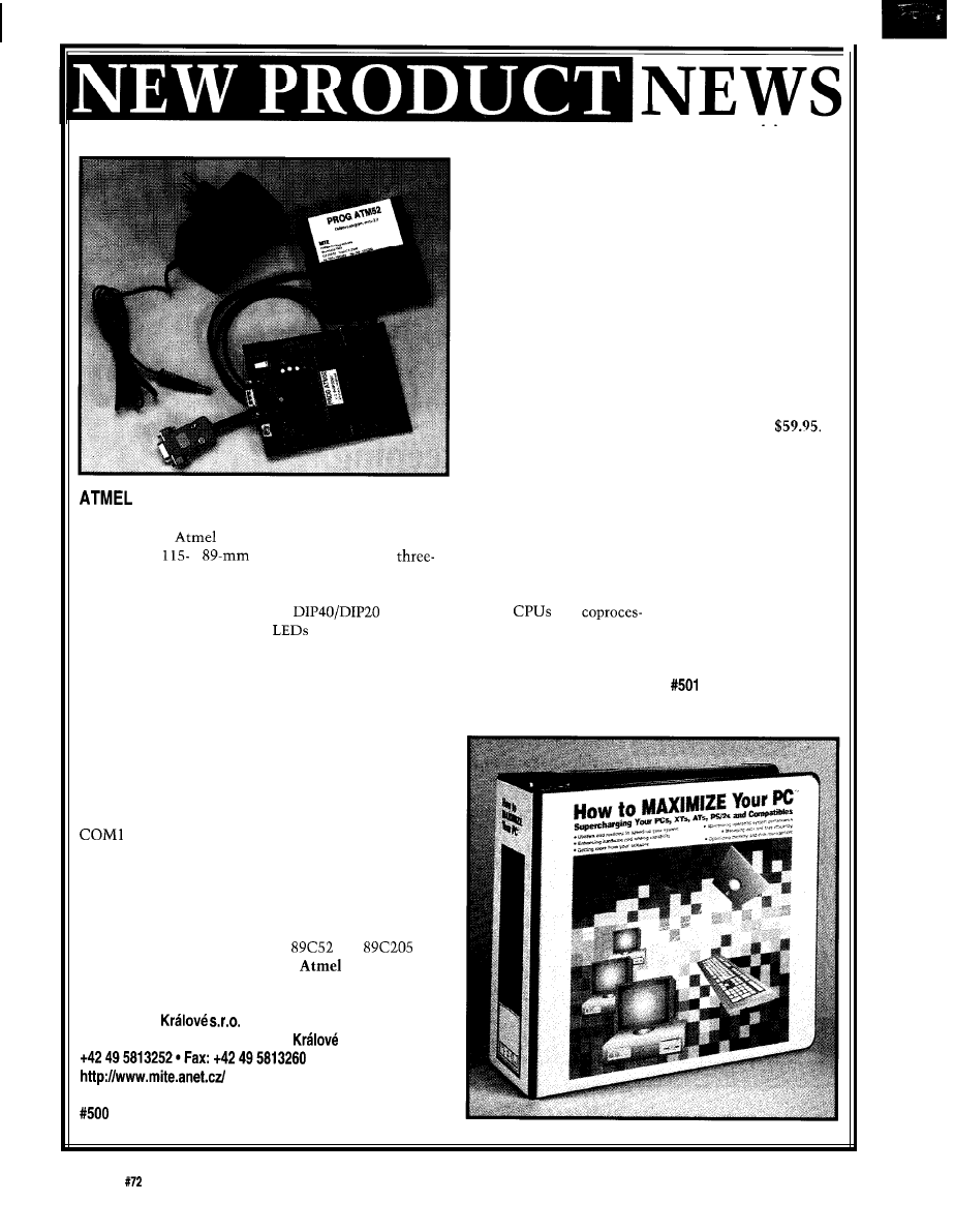
ATM52 PROGRAMMER
MITE offers a simple, inexpensive way to program the
AT89 series of
processors. The PROG ATM52
consists of a
x
printed-circuit board,
wire null-modem cable, AC adapter (230 VAC to
12 VDC), and diskette with PC software.
The PCB includes a universal
socket for
a programmed processor, two
indicating power and
busy states, a DE-9 connector for RS-232 communication
with a PC, and an adapter plug.
All operations such as reading, erasing, programming,
blank checking, verifying, lock-bits setting, checksum
counting, or buffer editing are accomplished by the soft-
ware. The software requires at least MS-DOS 3.3, 80286
or higher processor, 640-KB RAM, hard drive, and a
CGA, EGA, VGA, or HCG monitor. It runs under DOS,
or it can be executed from Windows in graphics mode
The user can change program configurations such as
or COM2 and the type of processor. The software
supports a mouse, and brief help is included. Two types
of files are supported: binary and Intel hex format.
The PROG ATM52 programmer sells for $99 in single
quantity ($80 per unit in lo-unit quantities). A complete
evaluation kit consists of an 805 1 assembler, 805 1 simu-
lator, PROG ATM52, samples of
and
1,
and datasheets. The Starter Pack
52
costs
$115
apiece ($90 per unit in lo-unit quantities).
MITE Hradec
Veverkova 1343
l
CZ 500 02 Hradec
l
Czech Republic
Edited by Harv Weiner
PC TROUBLESHOOTING BOOK
An excellent guide to
IBM-compatible equipment
and general PC system
troubleshooting and en-
hancement is available from
WEKA Publishing. How to
Maximize Your PC,
edited
by Steven S. Ross, is written
in simple terms and gives
straightforward information
about PC hardware and
software.
The book is presented
exactly as the buyer needs
it, enabling anyone to assess
their own computing re-
quirements. The work offers
hints and recommendations,
including many caveats not
found in manufacturers’
literature.
Major topics include IBM
standards and compatibility
issues,
and
sors, operating systems
including Windows 95,
programming language op-
tions, applications software,
hardware, peripherals
(cables, printers, mo-
dems), enhancement
guidelines, networks, and
software tips.
Each section of the
ring-bound volume deals
with typical questions,
describes common prob-
lems, and outlines steps
for remedial action. Peri-
odic updates are available
direct from the publisher.
Jensen Tools is offer-
ing this book at
This price includes a free
software disk containing
many useful PC utilities.
A free copy of the 1996
Jensen Master Catalog
is
also available.
Jensen Tools, Inc.
7815 S. 46th St.
Phoenix, AZ 85044
(602) 968-6231
Fax: (602) 438-l 690
8
Issue
July 1996
Circuit Cellar INK@
SURGE PROTECTORS FOR
NETWORKS
The Patton Models 570 and 580 Surge Protectors con-
nect directly to Category-5 data lines to protect hosts,
workstations, and communications equipment from data
loss and damage due to lightning, ESD, EMR, and other
surge hazards. The environments protected include Fast
Ethernet
ATM, and RS-422.
The units connect
to Category-5 cable using
modular RJ-45 jacks. Surges are diverted to a chassis
ground through a heavy-duty braided metal strap. Both
models are EIA/TIA TSB-40A Category-5 certified and
also comply with IEC Standards 801.2, 801.4, and 801.5.
Near End Crosstalk (NEXT) exceeds -43
at 100 MHz,
making the units appear to the network as a few inches
of Category-5 cable.
The Model 570 installs at the point-of-use, connecting
directly to terminal and communications equipment. It
has been tested to withstand IEC 801.5 Class-2 surges
(1
The Model 580 installs at barriers (e.g., building
entrances, between floors, and electrical panes). The 580
withstands IEC 801.5 Class-3 surges (2
Prices for the Patton Model 570 and 580 are $99 and
$159, respectively.
Patton Electronics Co.
7622 Rickenbacker Dr.
Gaithersburg, MD 20879
(301) 975-l 000
Fax: (301) 869-9293
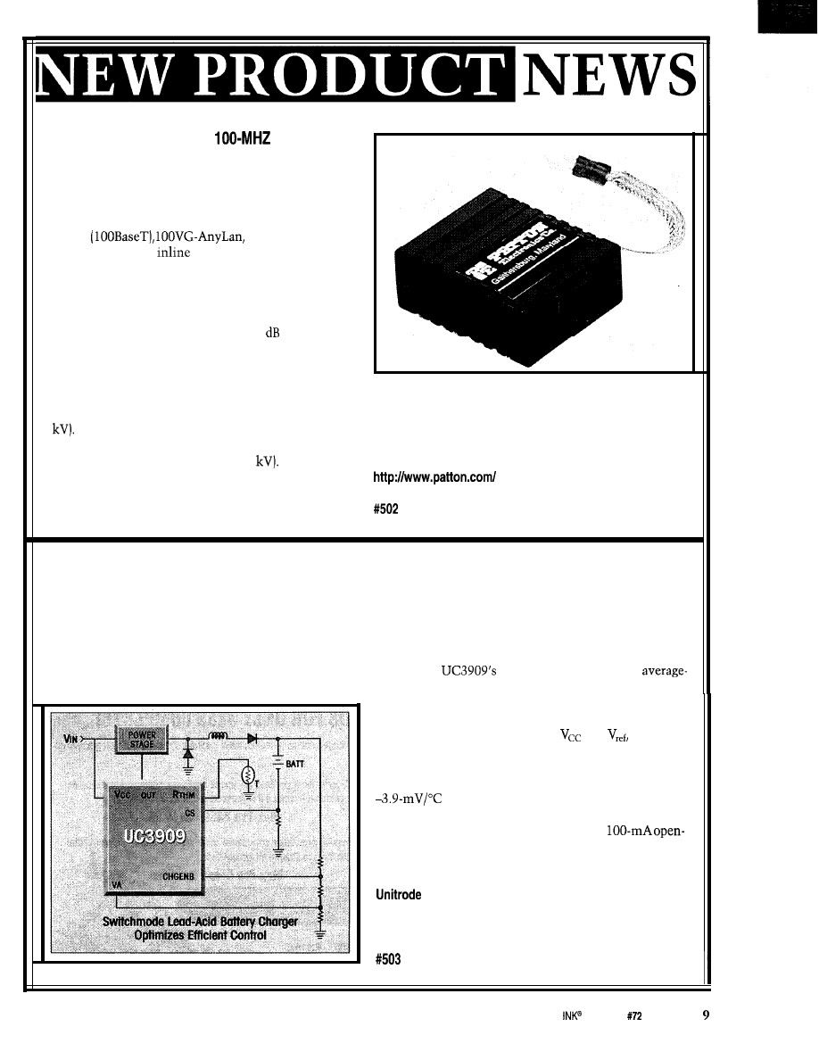
LEAD-ACID BATTERY CHARGER
Unitrode’s new UC3909 family of switch-mode lead-acid battery chargers combines charge-state logic with aver-
age-current PWM-control circuitry for greater efficiency in high-current charge applications. The UC3909 provides
accurate and efficient battery charging for emergency lighting, security systems, telecommunications, lawn mowers,
UPS backup power, and the automotive industry.
Featuring a thermistor interface which tracks battery requirements over temperature, the device provides precise
charge control for greater charge acceptance and longer battery life. The
voltage-control loop with
current limiting accurately controls charge rate from trickle to overcharge.
Four internal charge states with status bits report
accurate charge information at all times. The chip uses
undervoltage lockout to monitor
and
ensuring
sufficient supply voltage before output switching begins.
Additional circuit blocks include a differential-cur-
rent sense amplifier, a 1.5 % voltage reference, and a
thermistor linearization circuit. Voltage and
current error amplifiers, a PWM oscillator, comparator
and latch, charge-state decode bits, and a
collector output driver are also included.
The UC3909 is priced at $4.27 in quantity.
Corp.
7 Continental Blvd.
l
Merrimack, NH 03054
(603) 424-2410
l
Fax: (603) 424-3460
Circuit Cellar
Issue
July 1996
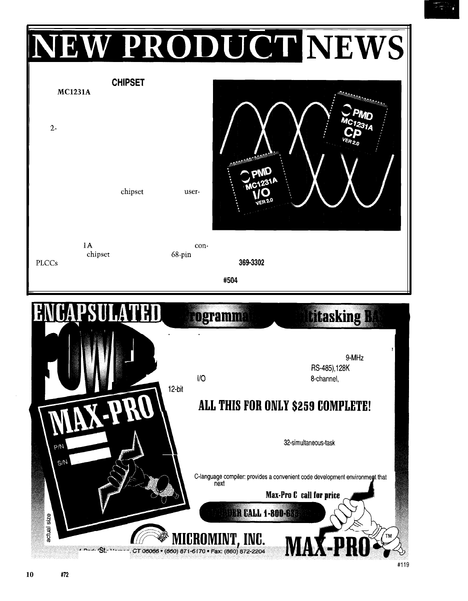
BRUSHLESS MOTOR
The
directly performs sinusoidal com-
mutation of brushless motors using the motor’s en-
coder signal to determine the phasing angle. Up to
two independent motor axes can be controlled, and
both and 3-phase motors are supported.
The “A” version adds the ability to detect commu-
tation errors on-the-fly for increased reliability. As
well, it supports a more sophisticated servo filter with
feedforward and a DC-bias offset. The ability to per-
form torque limiting under software control has also
been added.
Standard features of the
include four
selectable profiling modes: S-curve, trapezoidal, veloc-
ity contouring, and electronic gearing. Other features
include servo-loop closure, two directional limit
switches per axis, 16-bit DAC output, lo-bit PWM
output, and separate index and home signals.
The MC 123
is available in one- and two-axis
figurations. The
is packaged in two
and sells for $85 in quantity.
Performance Motion Devices, Inc.
97
Lowell Rd.
l
Concord, MA 01742
(508)
l
Fax: (508) 369-3819
Max-Pro is Micromint’s latest miniature encapsulated C-language, assembly, or
BASIC programmable controller. Max-Pro comes as a no-option, full-featured module
ready to assume the toughest embedded tasks. Packed inside is a
processor
with 6 counter/timers, 3 serial ports (two RS-232, one
bytes SRAM,
28 parallel lines, hardware real-time clock, and an
multiranging
ADC. Simply plug in a development system EPROM or compiled code and go.
We also offer two PC-based software development packages to make your programming
job easier:
Multitasking BASIC compiler: super fast,
compiler that creates
code like an interpreter but executes it with the speed of a compiler.
Max-Pro BASIC
$149.00
is the
best thing to straight assembly code.
4 Park
l
Vernon,
Issue July 1996
Circuit Cellar
INK@
CALLER-ID INTERFACE
Compared to
priced modems and units
costing five to ten times
as much, the
ITU
ID-to-PC Interface
is a
price and performance
breakthrough. The inter-
face measures only 2.25”
x 3” and can be plugged
directly into any spare
PC serial port.
source code is included
to
transform a PC into an
DOS- and
based software with
source code is supplied in
Visual Basic, and the
software source code is in C.
The ITU
PC Interface kit is available
for $39. Each unit comes
with a
money-back
guarantee and
war-
ranty.
ITU Technologies
3477
Ct.
(513)
574-7523
Cincinnati, OH 45248-3026
Fax: (513) 574-4245
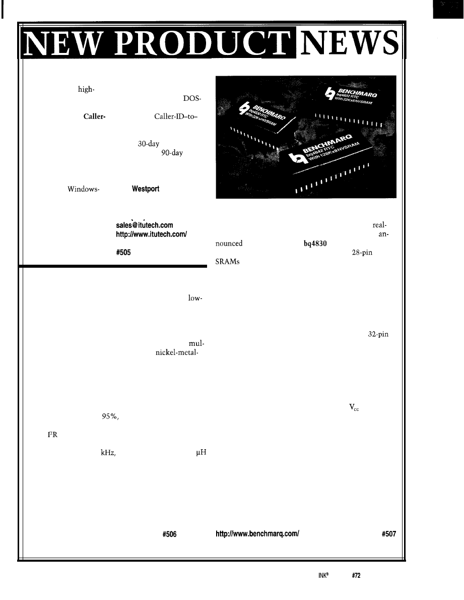
VERSATILE RTC MODULES
advanced Caller-ID box
Module products that incorporate a low-power
and to integrate Caller ID
time clock (RTC) and nonvolatile SRAM have been
into other applications.
by Benchmarq. The
Real-Time Clock
The Windows-software
module
directly replaces industry standard
DIP
and also fits into many EPROM and EEPROM
sockets.
SWITCHING REGULATOR OPERATES
OVER 3.5-36-V INPUT
Linear Technology has introduced the LTC1435
noise DC/DC voltage converter. The LTC143.5 is based
on a fixed-frequency current-mode architecture that
achieves efficiencies up to 95% over an input voltage
range of 3.5-36 V. This switching regulator is particu-
larly useful in portable designs that use a variety of
ticell battery packs, such as lithium-ion,
hydride, and nickel-cadmium batteries, where the volt-
age can vary from 4 V for discharged nickel types to over
30 V for wall adapters.
The LTC1435 drives N-channel MOSFETs instead of
more expensive P-channel MOSFETs. These N-channel
MOSFETs have lower on-resistance, enabling conversion
efficiencies to approach
even at load currents in
excess of 5 A. Their lower on-resistance results in re-
duced
losses, greater efficiency, and cooler operation
than P-channel MOSFETs. Switching frequencies can be
programmed up to 400
so inductors as low as 10
can be used to save board space.
The LTC1435 is available in 16-lead SOIC and SSOP
and costs $4 in 1000 quantity.
Linear Technology Corp.
1630 McCarthy Blvd.
Milpitas, CA 95035-7417
(408) 432-l 900
Fax: (408) 434-0507
The bq4830 provides nonvolatile SRAM by combining
an internal lithium battery with a 32 K x 8 CMOS
SRAM, a quartz crystal, clock, and power-fail chip. The
chip provides IO-year minimum data retention and un-
limited write cycles.
The bq4832 and bq4842 provide full CPU supervision
along with the same features as the bq4830. In a
DIP module, the bq4832 provides a watchdog timer,
power-on reset, alarm and periodic interrupt, power-fail
and battery-low warning, along with the low-power RTC
and a 32 K x 8 nonvolatile SRAM. The bq4842 can re-
place the bq4832 to provide a 128 K x 8 nonvolatile
SRAM.
The three modules also contain a power-fail detect
circuit that deselects the device whenever
falls below
tolerance, thus providing a high degree of data security.
All modules are shipped with the battery electrically
isolated to provide maximum battery capacity. The bat-
tery remains disconnected until the first application of
VW
Quantity prices are $18.75 for the bq4830, $20 for the
bq4832, and $42.50 for the bq4842.
Benchmarq Microelectronics, Inc.
17919 Water-view Pkwy.
Dallas, TX 75252
(214) 437-9195
Fax: (214) 437-9198
Circuit Cellar
Issue
July 1996
11
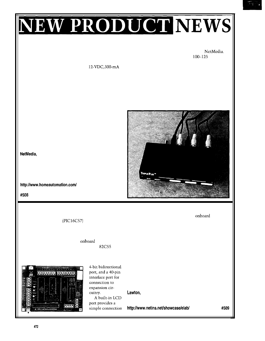
MICROPROCESSOR-CONTROLLED VIDEO MODULATOR
A three-channel, microprocessor-controlled, programmable digital video modulator is available from
The Triple Play has three modulators which cover video channels UHF 14-69 or cable 70-94 and
with pre-
cise, digital control.
The Triple Play comes with its own
power supply. It takes standard video and audio input from
home video cameras, security cameras, video recorders, laser discs, and video games to provide closed-circuit televi-
sion channels for distribution throughout the home or business.
The Triple Play features a built-in video amplifier with external gain control, internally generated test bars to
allow individual-channel setup without a video source, and a built-in video sequencer to display multiple video
sources one after the other on the same channel.
For example, the Triple Play can be used in a sequencer mode in a security application to view the front door, then
side yard, then back door. The unit can be used in sequencer mode alone, with more than one Triple Play, or with a
single-channel modulator MMOD70. Either MS-DOS
setup software
or the Serial Link setup-no software
needed-is required to program the video-sequencer
mode.
The Triple Play sells for $149. The MS-DOS software
and cable for programming the unit and/or the MMOD70
modulator is $49. The Serial Link setup is also available
for $49.
Inc.
10940 N. Stallard PI.
Tucson, AZ 85737
(520) 544-4587
Fax: (520) 544-0800
sales8 homeautomation.com
PIC MICROCONTROLLER
The PICPlus microcontroller board uses a RISC-archi-
tecture microcontroller
running at up to
20 MHz. It is ideal for a wide variety of applications such
as robotics and motion control, front-end control panels,
alarm systems, and embedded-control systems.
The PICPlus board includes an
power regula-
tor for battery operation and two high-speed
par-
allel interface chips for TTL compatibility. It also has
two byte-wide digital output ports, one byte-wide digital
input port, one
to most liquid crystal displays, and an
O-5-V
analog-to-digital converter directly interfaces to a wide
variety of sensors. I/O is greatly simplified due to the
low-level routines supplied with the controller. Conve-
nient connection to all ports and power lines is provided
by 36 terminal blocks
The board is programmed using either an 805 1 -like
assembly language (the PASM assembler is included) or
Microchip’s original instruction set. With a PIC micro-
controller, device programmer, and UV eraser, virtually
any embedded control application can be implemented.
The PICPlus microcontroller board starts at $239.
E-LAB Digital Engineering, Inc.
P.O. Box 246
IA 51030-0246
(712) 944-5344
Fax: (712) 944-5501
12
Issue July 1996
Circuit Cellar INK@
Alternative
Debugging Techniques
In-Circuit Emulators
A Single-Wire
Development Interface
Designing with
Flash Memory
LSI-11 Simulator on a
Personal Computer
Alternative
Debugging
e often find our-
effective tools than we’d
like. An ICE isn’t available because the
processor is too new, too old, or too
fast. The tools may be available, but
the project is too low profile or too
short term to warrant expensive, spe-
cialized debugging tools.
These problems are caused by the
highly CPU-specific nature of tradi-
tional hardware-based debugging tools,
which become obsolete. Even updated
versions of familiar processors often
require new debugging hardware.
The trend toward surface-mount
processors adds more complexity and
expense. High-density, high-pin-count,
surface-mount package probes are
expensive and finicky.
Designing emulators that interface
to a CPU socket is even more difficult.
Today’s
have shorter cycle
times, making the CPU-to-target inter-
face timing much more critical.
Since
incorporate internal
caches, prefetch queues, and pipeline
architectures, it’s increasingly difficult
to design hardware that properly emu-
lates the processor at the CPU
face.These factors add up to expensive,
nonadaptive development tools.
In this article, focus on inexpen-
sive, processor-independent,
assisted debugging techniques.
UNIVERSAL HARDWARE
INTERFACE
To develop hardware-based develop-
ment tools tolerant of changes to the
CPU speed, package, and bus timing,
we have to design to a different hard-
ware interface.
14
Issue July
1996
Circuit Cellar INK@
It should allow hardware debugging
tools to adapt quickly to new proces-
sors or processor derivatives. Ideally,
more generalized hardware can be used
on a variety of targets, regardless of the
make, model, speed, or processor fla-
vor. It should even work for CPU cores
buried within an
Believe it or not, most embedded
systems already have such an inter-
face! The target’s EPROM or flash
socket is a well-documented,
understood, and stable interface. Most
importantly, its specifications are
independent of the target’s processor.
Timing at this socket is usually
much less critical than at the proces-
sor interface. If the processor’s cycle
times are significantly faster than the
memory device’s capabilities, the
target board incorporates a cache or
memory-interleaving techniques to
decouple the high-speed CPU interface
from the memory-socket interface.
Manufacturers of memory-interface
devices can design their products to an
EPROM’s less stringent and standard
mechanical, functional, and timing
specifications. These features add up
to less expensive, more flexible devel-
opment tools.
So, here’s a processor-independent
hardware interface already present on
most embedded targets. What can we
do with it? Let’s discuss some hard-
ware-based tools that interface to the
target’s memory socket and techniques
for using them.
MEMORY-INTERFACE
DEVELOPMENT TOOLS
Memory-interface-based develop-
ment tools are available with a variety
of features. Here are some of the major
features and debugging techniques
each one enables.
The base-line functionality of these
tools is simple EPROM emulation. An
EPROM emulator is little more than
SRAM with a separate download con-
nector. It plugs into a memory socket
in place of the EPROM and connects
to the development system through a
serial or parallel connection.
It enables you to quickly load new
code images into its internal SRAM.
When the download is complete, it
looks like an EPROM to the target.
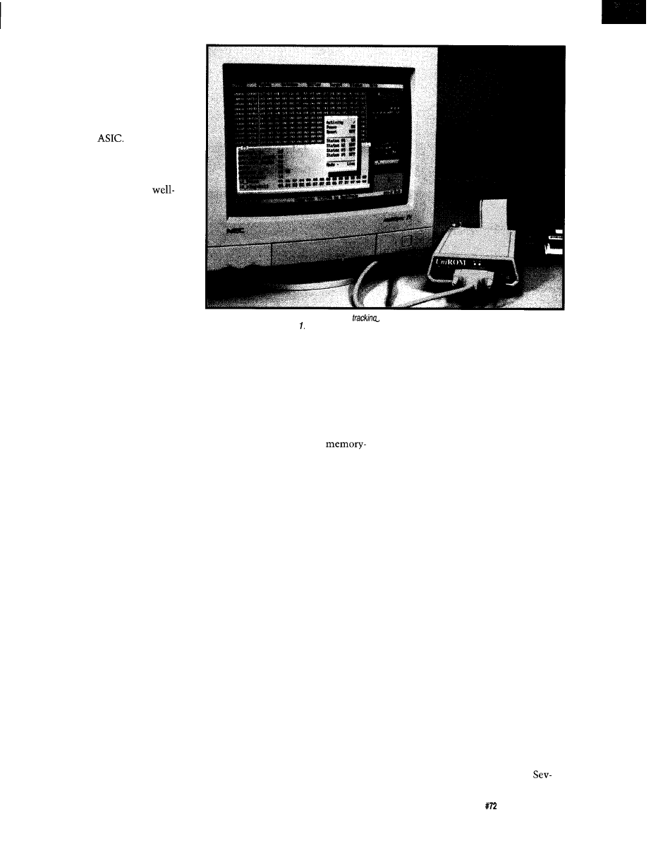
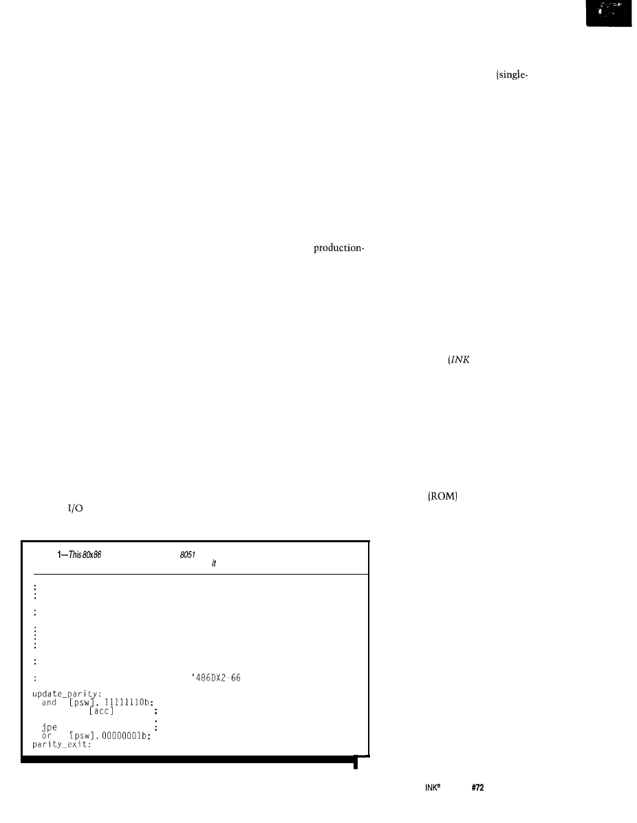
Photo 1-A
live-access emulator is shown here
down a null-pointer reference. The data shown in the live
editor is reproduced in Figure
While this function doesn’t actually
debug, it speeds up development con-
siderably. The reduced turnaround
time permits debugging techniques not
feasible before. Even with the best
The next logical step in
interface hardware is an EPROM emu-
lator that accepts target-write cycles.
development tools, a basic EPROM
You can then plug into EPROM, flash,
and SRAM sockets. More importantly,
emulator easily earns its keep.
it provides new debugging techniques
since the target can write information
into unused memory locations.
Write-back capability enables moni-
tor programs or software-debugger
kernels to load applications and write
software breakpoints into the target’s
code space. This feature may be all
you need to use these tools on your
target.
Some memory emulators have vir-
tual UART options. A virtual UART is
a memory-mapped communication
port, which adds a serial port to any
target with a memory socket. An extra
port can be very useful during debug.
These ports can be read/write or
read only. The read/write type works
like a standard UART. The target ap-
plication or monitor program reads and
writes its status, transmit, and receive
registers like any other UART.
The read-only style permits full
bidirectional communications without
target-write cycles. The target “trans-
mits” by performing a particular se-
quence of reads from selected memory
addresses. The accessed addresses and
their order encodes the transmit data.
Read-only ports are useful if the
target is incapable of writing to code
space. Some Harvard-architecture
processors don’t have opcode for writ-
ing to their code spaces. Other targets
specifically exclude write cycles from
the EPROM-socket chip selects. Still
other targets use single-direction data
buffers between the processor and the
EPROM socket.
Another read-only-style advantage
is the ability to communicate without
the target modifying its code space.
This feature may be desirable or even
required during acceptance testing of
some products.
Live access offers the ability to read
and write the target’s memory while
the target is executing from that same
memory without imposing any restric-
tions on the target’s accesses. This
important feature enables many new
debugging techniques, especially for
real-time targets that can’t tolerate
breakpoints or single-stepping.
When looking at emulator specifica-
tions, evaluate this one closely.
Circuit Cellar INK@
Issue
July 1996
1 5
methods let the host access target
memory while the target is running.
Side effects vary, depending on how
the manufacturer achieves this goal.
Some emulators depend on target
arbiters or wait-state hardware for
arbitration. This approach may work
for particular targets, depending on the
availability of these resources, the
target documentation available, and
the firmware’s tolerance of intrusions.
Other emulators impose additional
restrictions on the target’s timing at
the EPROM socket, such as a mini-
mum recovery time between accesses.
A good memory-interface debugging
tool provides memory emulation and
the support features that fit the me-
chanical, electrical, and timing charac-
teristics of an EPROM. To achieve
this, they cannot place any restrictions
on how the target uses them. Note
that an EPROM is always ready and
has no recovery-time restrictions.
When shopping for an emulator
with a live-access feature, look for one
that is completely transparent to the
target. Verify that the live accesses
work in any target designed to accept
standard EPROM or flash devices,
without imposing additional con-
straints. For maximum flexibility and
compatibility, avoid wait-states or
request/grant approaches.
From now on, 1’11 assume your emu-
lator allows live host-side access with-
out any restrictions on the target-side
accesses-this is very important.
The target fetches opcodes, oper-
ands, and data from the emulator. No
processor double reads to verify the
data’s integrity or checks semaphore
flags before starting an opcode fetch.
We want to asynchronously access the
memory without coordinating with
the target application.
Hardware trace is a new, advanced
feature for memory emulators. Trace is
similar to a logic analyzer, but specifi-
cally designed for firmware debugging.
It lets you trigger on
type events and shows you the events
that led up to the trigger condition.
Trace allows you to trap things like a
target Write to address 0x8000 with
data greater than
A trace option is always connected
to the target and properly set up to
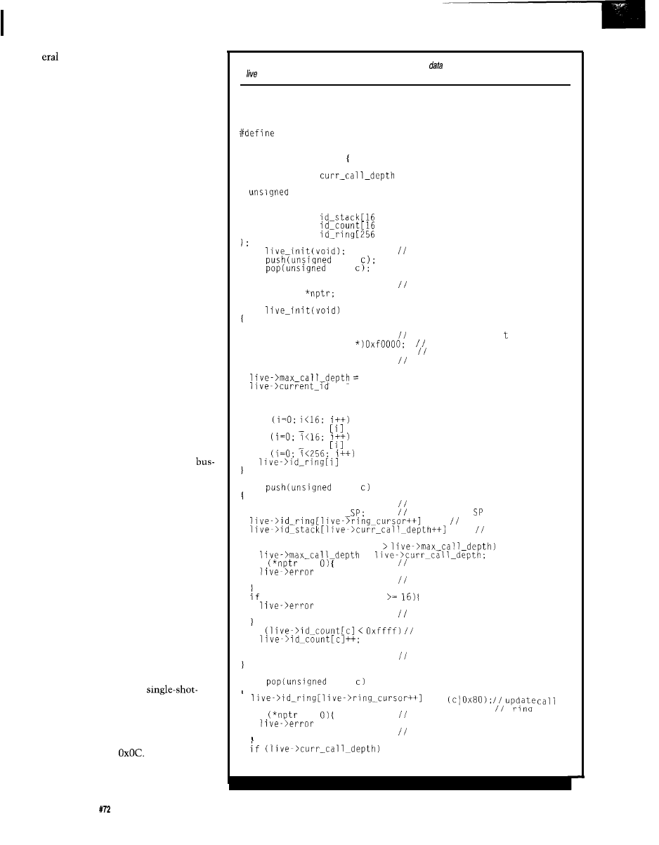
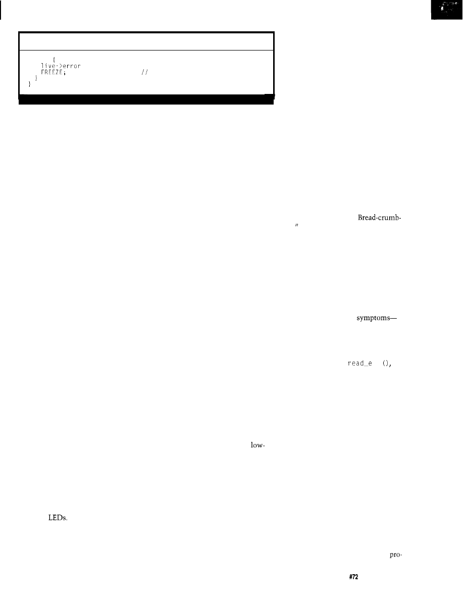
Listing l--These routines log trace
and status information to
structures in the target’s memory space.
A access-type memory emulator can watch these structures to aid debugging.
#include <stdio.h>
#define OVERFLOW 1
#define UNDERFLOW 2
NULL-ENTER 3
#define NULL-EXIT 4
#define FREEZE
while(l);
typedef struct WATCH
unsigned char current-id:
unsigned char
unsigned char max_call_depth;
char error:
unsigned int
current_sp;
unsigned char ring-cursor
unsigned char
unsigned int
unsigned char
void
void
char
void
char
local prototypes
static struct WATCH *live:
unsigned int
local variables
void
unsigned int i;
nptr =
NULL:
intentional NULL p
live = (struct WATCH
place log data
data space
live->error = 0;
initialize everyth
live->curr_call_depth = 0;
0;
= 0;
live->current_sp = 0;
live->ring_cursor = 0;
r assignment
in unused
ng
for
live->id stack
for
live->id count
for
= 0;
= 0:
= 0;
void
char
live->current_id = c;
update current ID
live->current_sp =
and current
= c; update the call ring
= c: update call-
// stack tracking
if (live->curr_call_depth
=
if
!=
somebody trashed 0
= NULL-ENTER:
FREEZE:
freeze system to see who did it
(live->curr_call_depth
= OVERFLOW;
FREEZE:
catastrophic error. freeze!
if
update the count for this ID
else
FREEZE:
freeze to evaluate
void
char
=
if
!=
somebody trashed 0
= NULL-EXIT;
FREEZE:
freeze system to see who did it
live->curr_call_depth--;
(continued)
18
Issue
July 1996
Circuit Cellar INK@
Listing
l-continued
else
= UNDERFLOW;
MAJOR PROBLEM, freeze!
interpret signals in target terms. You
make trigger specifications and trace
filter criteria from address, data, and
control-signal values, ranges, or edges.
Since the trace board connects to
the memory socket, it sees the same
address, data, and control lines the
memory device sees. The address and
data signals are usually common to the
rest of the circuit. The analyzer has a
more global view than you’d think.
Additional trace-option inputs let
you trigger on other chip selects or I/O
signals. Since these devices usually
share the same address and data lines
as the EPROM, it’s easy for the trace
board to trace data, I/O, and code ac-
cesses.
You can also connect upper address
lines to the extra inputs. This action is
rarely necessary after you have the
select circuitry debugged.
Finally, some memory emulators
let you customize them with your own
code. Some manufacturers provide
libraries or developers’ kits for you to
write your own programs. The more
advanced the emulator, the more valu-
able this feature becomes. A live-ac-
cess emulator with a trace that allows
custom program control is the ulti-
mate debugging tool.
DEBUGGING TECHNIQUES
We
engineer code to minimize the
possibility of errors-but bugs occur
every time. When we debug firmware
without expensive tools, we usually
fall back on several basic techniques.
Smaller incremental steps isolate
bugs to specific sections of code. Small
test routines reveal how different parts
of the target act and interact.
Code patches wiggle spare port pins
and flash
They dump messages
out serial ports. Using other tech-
niques, firmware generates nonstand-
ard bus cycles (like writes to EPROM
or nonexistent I/O devices) which are
benign to the target, but create specific
stimuli that a scope, logic analyzer, or
other hardware can capture.
These techniques communicate
debugging information to the outside
world via basic “
I
made it to here”
trace information or an alarm signal
like “I received a null pointer.”
Memory emulators offer a quicker
“spin” on code changes. With the
shorter cycle, you can try things you
wouldn’t if you had to burn EPROMs.
It’s now feasible to make test patches
to your source code and observe the
results in little more time than it takes
to run a new make.
With a memory emulator, you
think about debugging differently. For
example, you can move the old “Blink
the LED (hardware trace device]” state-
ments around in the code to figure out
where the firmware starts thinking on
its own.
You can comment out pieces of
suspect code, hard code configuration
items, or change timing-loop con-
stants. It’s possible to freeze the pro-
gram with Ha 1 t instructions at critical
or informative locations. Quick code
updates let you add tests to the source
code instead of patching object code.
Memory emulators enable you to
quickly test what-if scenarios. This
basic troubleshooting technique is still
a major step up from dry-run desk
checking.
In addition, with simple and
cost memory emulators, you can di-
rectly test your development system.
By eliminating the need to schedule
time on the ICE or wait on EPROM
erasers or programmers, you can often
work entirely from your office.
It is quite possible (but painful) to
debug entire projects with nothing
more than a memory emulator and an
LED. You find yourself saying, “If only
I knew what x is at this point” or “Is
the FIFO buffer overflowing?”
You find answers to these questions
by making patches to the code. You
can turn on the LED if x exceeds a
specific value or if the FIFO pointer
nears its overflow point.
However, it’s more useful to see
these variables (and many others) to
determine just how bad they are or
exactly how they got in that shape.
STATIC BREAD-CRUMBING
Memory emulators with target
write-back capability add several de-
bugging techniques to our toolbox.
First of all, target write back lets the
target application write debug mes-
sages into unused memory locations.
When the target goes stupid, you
can hold it in reset and read the emu-
lator’s memory to view those mes-
sages. I call this “Static
ing.
The target application leaves bread
crumbs sprinkled throughout memory
to help you determine where it left the
road. Other bread crumbs give us clues
about why the firmware is in the
weeds. Static bread-crumbing is an
advanced version of “Flash the LED.”
With basic EPROM emulators, we
hypothesize the problem’s cause based
on very few observable
perhaps only the LED. We plan how to
test that hypothesis, patch the code,
and observe the results.
After several iterations, we may see
that the code froze in
e for
example. So, we shift our focus to that
routine. After more iterations, we
determine that the code is waiting for
the EPROM to set its ready bit.
Eventually, we find we violated a
minimum clock width or setup param-
eter to the EEPROM, so it ignored us.
To find the offending code, it takes
several well-thought-out tests.
Target write-back capability lets us
observe more data on each iteration.
With more clues, you can make a more
intelligent hypothesis for each test,
reducing the number of iterations
required to zero in on a bug.
However, a simple trick shows the
offending routine immediately. If each
procedure writes a unique ID code to a
single memory location when it is first
entered, then when the target freezes,
this location holds the last active
Circuit Cellar
INK@
Issue
July 1996
1 9
cedure’s
ID. A quick look at that loca-
tion tells us which routine locked.
You can expand this concept by
having each routine write its ID, the
current stack pointer value, and any-
thing else of interest to consecutive
memory locations. Now you know
what was running and what the last
values of these critical items were.
Another simple trick is to assign a
different bread crumb to each proce-
dure. Each procedure increments its
own bread crumb each time it ex-
ecutes. Postmortem analysis of these
counts provides clues to unexpected
interaction between modules or exces-
sive use of error-recovery routines.
Call-stack tracking is another use-
ful technique. It creates a call-stack
structure that tracks stack activity.
In its simplest form, a macro or
procedure call placed at the beginning
of each procedure pushes the proce-
dure’s ID onto the simulated stack.
Another macro before any return state-
ment pops the simulated stack.
This call-stack structure reveals the
sequence of calls causing the problem,
as well as the maximum call depth
encountered. This structure often
reveals unexpected interaction be-
tween procedures, unplanned recur-
sion, or circular references.
Another useful bread crumb is a
call-history buffer, which is simply a
circular buffer that holds the
of
the last called procedures. A single
pointer shows the last ID entered.
If the emulator is in the target’s
RAM socket, the program’s variables
are there for postmortem inspection.
You can also achieve this by changing
the target’s decode circuitry to map
code and data into the emulator.
A target often has unused memory
space you can decode into the emu-
lated space. The emulator then pro-
vides extra
memory space for
debugging, even if the application fills
its normal ROM and RAM space.
DYNAMIC BREAD-CRUMBING
If you’re lucky enough to have an
emulator that gives truly nonintrusive,
live access to the target’s memory
while the target is running, you then
have many powerful debugging tech-
niques.
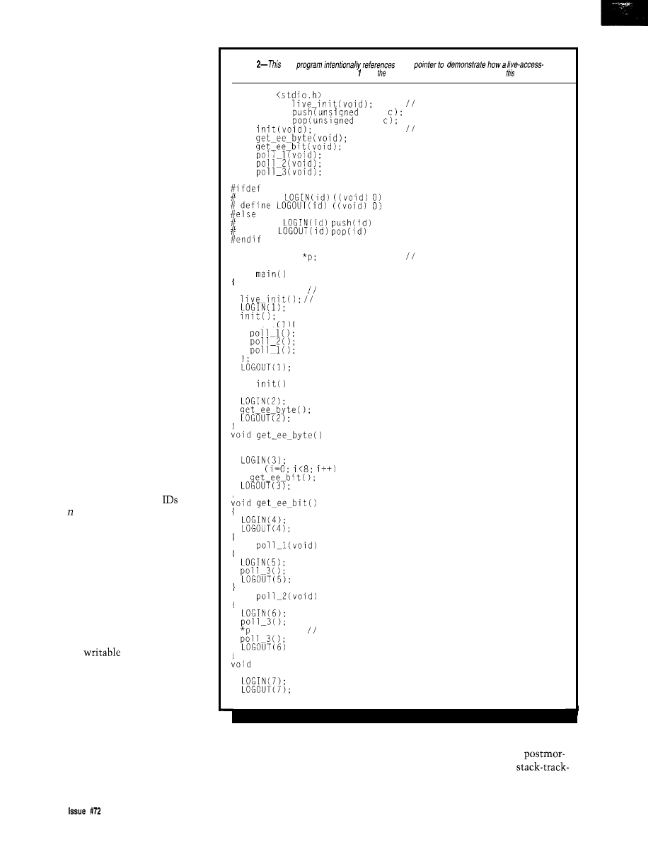
Listing
test
a null
capable emulator helps track bugs. Figure shows trace information generated by program.
#include
extern void
extern void
char
external prototypes
extern void
char
void
void
local prototypes
void
void
void
void
NDEBUG
define
define
define
unsigned char
local variables
void
p = NULL;
to prove the point, we force p to point to NUL
initialize data logging
while
void
unsigned char i;
for
void
void
= Oxaa ;
intentional use of a NULL pointer!
poll-3 (void)
You can stimulate the target and
And, you can use these techniques
observe the results in real time! And,
in real time, rather than in
you can watch the firmware’s data
tern. You can look at the
structures while the target is running.
ing structures and other bread crumbs
20
July 1996
Circuit Cellar INK@

without stopping the target. I call this
“Dynamic Bread-crumbing.”
If the target maps its variables into
the emulator’s space, you can watch
them without affecting its perfor-
mance. You can watch things like
task queues, current task ID, error
indicators, and FIFO and ring pointers,
without adding code to the applica-
tion.
It’s important to understand what
this can and cannot do for you. Any
live viewing of a target’s memory is a
polled view of that memory.
You get to nonintrusively view
trends, verify certain variables are
staying within bounds, monitor statis-
tics, or watch for error conditions. If
you initialize
and other dynamic
data structures to a known value, you
can often tell how full they get during
operation.
If your live editor lets you freeze the
watch screen, you can even take snap-
shots of the current state of the data
you are watching without affecting the
target. You can evaluate the health of
data changing too fast for analysis.
For example, if you’re watching a
ring buffer and its associated pointers,
the data changes rapidly as the applica-
tion fills and empties the ring. Freez-
ing the display lets you evaluate the
contents of the ring and exactly how
full it is at any time.
A live polling of the emulation
memory doesn’t let you capture
cycle events or create any type of trig-
ger when the application accesses a
specific memory location or writes a
specific value to a specific location.
These results are usually obtained
from check routines to the firmware
that detect the error, write error-mes-
sage bread crumbs, and optionally halt.
The firmware actually traps the event.
The live editor shows exactly what
event happened and where.
If you’re looking for the cause of
mysterious changes to a memory loca-
tion (stray bullets), you need a logic
analyzer or a trace-board option with
advanced triggering capabilities.
The key point is that live polling
and editing of the emulation memory
creates a nonintrusive window into
the target’s operation. Live access is
distinctly different from hardware
tracing and is a very powerful tool.
Dynamic stimulation makes use of
an emulator’s live editor to change
memory while the-target is executing.
This functionality simulates external
conditions, devices, or data streams.
You can complete development of
interface code without actually having
the external equipment on hand. Even
if you have the other equipment, this
technique creates a more controlled
test of the firmware’s reaction to the
external device.
For example, while debugging one
end of a communication link, you can
simulate receiving packets from the
other end of the link. Simply insert the
packet into your receive ring buffer
and then adjust the ring pointers and
associated flags to indicate you re-
ceived the packet.
Remember, you can do this while
the target is executing-if you’re care-
ful. When you set the Full flag, the
target should react to the packet. Of
course, this example assumes that
Circuit Cellar
Issue
July 1996
2 1
your protocol is packet oriented and
that you’re using large enough ring
buffers to hold an entire packet.
By live writing to target memory,
you can force error conditions that
may be difficult to create in the out-
side world. In the previous example,
you could intentionally create a bad
packet and evaluate how the firmware
reacts to it.
Live writing can be used to com-
municate with the target. If you
want quick A/B comparisons be-
tween different buffer sizes, write
code to an agreed-on location to tell
the application which buffer size to
use.
The application checks this loca-
tion each time it uses that param-
eter. This approach is safer than
patching the buffer size directly.
It’s possible to do direct code
patching, but it requires careful
A live-access emulator and a soft-
ware debugger are an unbeatable com-
bination. The debugger lets you see
high-level data structure and set break-
points. The emulator minimizes the
debugger’s target resource require-
ments.
When the debugger lets the target
run at full speed, it becomes invisible.
At this point, the emulator’s live
current-id
error
current_sp
eb02
ring-cursor
id-stack
06 07
id-ring
0 1 0 2 0 3 0 4 8 4 0 4 8 4 0 4
8 4 0 4 8 4 0 4 8 4 0 4 8 4 0 4
8 4 0 4 8 4 8 3 8 2 0 5 0 7 8 7
8 5 0 6 0 7 8 7 0 7
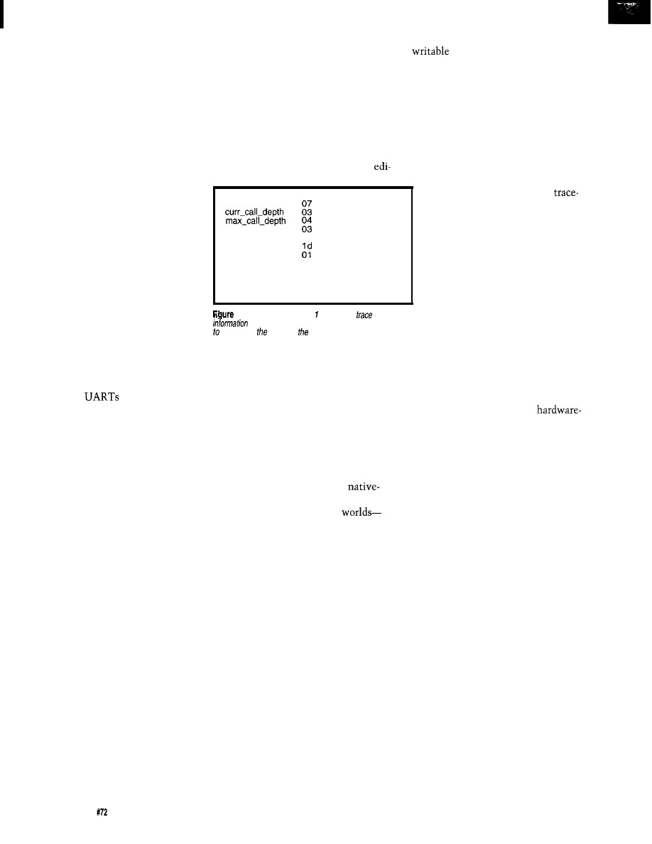
l--The
routines in Listing logged this
and status
when Listing 2 was executed. This dafa enables us
track
down source of null-pointer reference.
The trigger-out from the trace
generates an interrupt to the target
when the target accesses any loca-
tion within the specified range. If
you’re using a software debugger,
the interrupt causes a break.
The debugger references the
instruction pointer back to the
source code so you see the offending
code immediately. Most debuggers
also let you look at the call stack at
this point.
planning of the original code. Re-
member, you can’t create critical re-
gions by disabling interrupts. Nothing
holds off the live patch!
Virtual
primarily provide a
communications path for monitor
programs or software debuggers. Soft-
ware debuggers execute a small target
monitor program to gain access to
internal CPU resources and external
memory and I/O. The monitor com-
municates with the debugger through
a serial port or virtual UART.
The monitor is responsible for read-
ing and writing CPU registers, CPU
and target memory, and I/O spaces. It
also handles single stepping and patch-
ing in software breakpoints.
The debugger uses the host compu-
ter’s resources to cross-reference sym-
bols and to interface with the user.
A software debugger is useful for
single stepping, setting breakpoints,
and viewing data structures. Many
software debuggers include dynamic
modes of operation that let them inter-
rupt the target on a periodic basis and
to update watches.
A memory emulator with a virtual
UART and target write-back capability
is an excellent enhancement to a soft-
ware debugger. It eliminates two of the
software debugger’s most intrusive
target requirements: the need for a
serial port and extra debug RAM.
tor can help with the other real-time
techniques I’ve discussed.
For example, you set a breakpoint
with the software debugger, start the
target application, and then switch to
the live editor. From the live editor,
you force errors or simulate received
packets and see if the program hits the
breakpoint.
You then use the software debugger
to look at variables in their
language format. This combination
gives you the best of both
static and dynamic debugging.
However, some bugs are elusive. A
hardware-trace option captures a sub-
tle bug in the act, even if you have no
idea which code module is responsible.
For example, it’s difficult to deter-
mine exactly which line of code uses a
null pointer. Without hardware trace,
you’d place code at the start of each
procedure to check the bottom of data
space for corruption.
Most C compilers place a copyright
or the word “null” in this location to
reserve the space and allow them to
check for corruption. Your code sets a
bread crumb and freezes the program if
it detects a change to this location.
This technique narrows down the
suspects to something in the procedure
that calls the current one. Of course,
this only captures writes that land in
memory space. Reads won’t
trigger an error.
Also, this technique only works if
the write actually destroys data within
the range being checked. Checking an
extended range becomes too intrusive
to the target’s operation.
With a hardware trace, simply trig-
ger on any access to the start of the
data area. A hardware trace device
captures the events leading up to
the illegal access. Check the
buffer contents and call-stack bread
crumbs to see who is responsible
and what call sequence leads up to
the problem.
You can effectively use a
trace option with a software debugger
that doesn’t necessarily support trace
itself. The debugger may not interpret
the trace buffer information for you,
but the data is still available.
Additionally, you can use the trace
board’s triggers to implement hard-
ware breakpoints for the debugger.
Even without a software debugger,
you can trap the interrupt and bread
crumb the stack and register contents
for analysis or perform other actions
you feel appropriate.
THEORY IN ACTION
Listing 1 offers routines that em-
body some of these techniques. Of
course, you may want to expand or
condense them to fit your particular
application. Listing 2 is a minimal
program designed to create bugs.
You can leave these routines in
your source code without affecting the
performance of the final production
code. I modeled the functionality of
the ASS E RT macro supported by most
C compilers.
You can disable these macros by
defining ND E B U G. If you do not define
22
Issue
July 1996
Circuit Cellar INK@
ND E B G, the compiler includes the
code. This code is in C, but the con-
cepts port to any language.
If you include these macros as you
write
your code, you’ll find it’s pain-
less to build in this type of debugging.
When you start debugging, you can
refine exactly what data the pus h
and
pop
routines store and what
errors they check.
When enabled, these routines affect
the overall performance of your target
program. The degree of this impact
depends on how much data you log
and how often you call the routines.
However, logging at full memory band-
width minimizes the intrusion to an
acceptable level for most applications.
Note that in pus h you can check
a variety of error conditions and react
to the errors as you see fit. you’re
looking for catastrophic errors (like a
stack overflow or null-pointer usage),
Id-stack showsusthat
was called by 1
This infor-
mation narrows our focus to some-
thing that happened after entering
p
o
and before entering p o 1 1 _
In
this simple example, we can
easily review p
o
1
and find the
problem. In a more complex routine,
we may need to add more trace infor-
mation to narrow the search.
The i
i n g structure provides
additional clues. The data shows that
we successfully called and returned
2
before seeing the null-pointer
error.
3
and before the second call to
PO1
Since we look for null-pointer usage
at the entrance and exit of each rou-
tine, we know that the previous call to
1
did not cause the problem.
Therefore the problem occurred within
you may freeze the program to
Freezing the program eliminates the
possibility of the processor writing
serve the current state of all memory.
stray bullets into memory. When you
freeze the application, you may want
to disable interrupts so interrupt ser-
vice routines don’t change things. Of
course, you can log more or less data
as you see fit or check for specific error
conditions unique to a particular bug.
routineslet
you find the cause of stack overflows,
null-pointer usage, or unexpected re-
cursions. Simple modify these routines
to look for clues to any specific bug
you are tracking.
These same routines also provide a
framework for code profiling. you
have a live-access-type memory emu-
lator with a documented interface
library, you can write a simple polling
routine to read these data structures at
fixed intervals. Statistics gathered
from this data tell you the average and
maximum call depth and the relative
time spent in each routine.
Listing 2 shows a simple skeleton of
procedure calls. It serves no real pur-
pose, except to demonstrate the use of
these debugging techniques.
I intentionally referenced a null
pointer in the p
o
1
routine to
demonstrate bug tracking with a
access memory emulator. The program
freezes when pus h
detects a corrup-
tion to the bottom of data space.
Photo
1
shows the results of run-
ning the program on a ‘486 target
while monitoring the debug structures
with a live-access memory emulator.
Figure
1
offers
data.
This example corrupted the bottom
of data space in p o
The data
structures lead us to the culprit as
follows.
EMULATORS IN YOUR TOOLBOX
I’ve introduced a number of
purpose techniques for using memory
emulators for both static and real-time
debugging. Many of these techniques
are simple variations on old themes.
Others are only possible with the new
live-access emulators.
Regardless of what tools you have,
even the simplest EPROM emulator
has its place in your toolbox. You can
that more easily adapts to changes in
CPU technology.
Top-end emulators provide live
watching and editing of the target’s
memory, enabling debugging tech-
niques previously only available with
top-end, highly CPU-specific
Emulators capable of live editing are
available for under $600.
Of course, these devices and tech-
niques are only tools. Their real use-
fulness depends on your understanding
of how to use them. The answers they
provide are only as good as the ques-
tions you define.
q
Merrill is the founder and CEO
of
a company that special-
izes in memory-emulation devices.
has been involved in electronics
for over 20 years. You may reach him
at
(EPROM/flash emulator)
Romboy (EPROM emulator)
Grammar Engine, Inc.
921
Dr., Ste. 122
Westerville, OH 4308 1
(614) 899-7878
Fax: (614) 899-7888
HT Series (EPROM emulators)
Hobby-Tek
P.O. Box 462085
Garland, TX 75046
(214) 272-0202
Romem (EPROM emulator)
Development
4100
Ave., Ste. 104
San Jose, CA 9.5 117
(408)
Fax: (408) 296-5877
(Live-Access EPROM/
flash emulator)
(EPROM emulator)
P.O. Box 462101
Garland, TX 75046
(214) 272-9392
Fax: (214) 494-5814
routine. Cur
d tells us that we
More advanced emulators provide
detected this problem when we
hardware support for software
tered
gers. You get a development system
401 Very Useful
402 Moderately Useful
403 Not Useful
24
Issue
July 1996
Circuit Cellar INK@
In-Circuit
Emulators
Graham Moss,
Ross
Ken Mardle
Part 1:
hese days, we
Development
ssume that even
most mundane
Tool Options
contains a microcontroller executing
some sort of control program.
ectronic equipment
Users of such equipment expect
increasingly sophisticated features,
which in turn require increasingly
capable microcontrollers executing
increasingly complex code. To make
matters worse, commercial consider-
ations dictate ever shorter develop-
ment cycles.
Fortunately, the increased process-
ing power of modern microcontrollers
and parallel advances in
generation technology typically allow
control programs for microcontrollers
to be implemented with standard
level programming languages like C,
Pascal, or Modula-2. Large, complex
control programs are now designed and
coded in relatively short periods.
Unfortunately, as any seasoned
development engineer knows, im-
provements in code-generation tools
are only half the story-there remains
the human element. Developing code
for an embedded microcontroller can
be a real nightmare.
Developers still make mistakes and
omissions both in terms of design and
implementation. The number and
complexity of such errors roughly
follow the magnitude and complexity
of the overall control program. They
are exacerbated by the complexity of
the target microcontroller.
Indeed, the benefits
language code-generation tools bring
can be their greatest liability. They
provide an efficient way to generate
large amounts of complex buggy code.
In the past, time in design and cod-
ing dominated the overall develop-
ment cycle. Now, more time is spent
testing, debugging, and qualifying. So,
it’s critical that the overall develop-
ment effort be similarly well supported
with efficient debugging tools.
When searching for that last elusive
bug, your debugging tools can either
help or hinder depending on their qual-
ity, flexibility, functionality, and suit-
ability of purpose. In this series of
articles, we’ll describe the types of
debugging tools available and compare
their strengths and weaknesses using
the yardstick of transparency.
Afterwards, you’ll be in a good posi-
tion to see beyond the advertising hype
and to sensibly evaluate the genuine
strengths and weaknesses of the
myriad debugging tools available.
The series concludes with a descrip-
tion of the design of the hardware and
software components of
l-a
popular low-cost in-circuit emulator
(ICE) system designed by Philips to
support development using their wide
range of
1 -based microcontrollers.
WHAT’S NEEDED
Debugging tools should be as trans-
parent as possible. They shouldn’t
have side effects which mask a prob-
lem or introduce new ones. Users of
debugging tools should expect them to
place as few hurdles as possible be-
tween themselves and the solution of
their problem.
A wide range of debugging tools is
available today. Each vendor’s solution
represents a different set of design
goals and compromises intended to
address different types of debugging
problems.
Debugging systems differ in terms
of the scope and power of the control
and monitoring functions they offer.
And, just as importantly, they differ in
terms of the microcontroller resources
they “steal” to provide their control
and monitoring functions, and the
extent to which they interface with
the real world beyond the pins of the
microcontroller.
Costs vary from less than a hundred
dollars to the tens of thousands. While
cost is important in any purchase deci-
sion, it should be kept in perspective.
26
Issue
July 1996
Circuit Cellar INK@
A cheap debugging tool may hinder
more than help. It can quickly end up
gathering dust.
At best, you waste the purchase
price of the unit. But, true costs may
be much higher in terms of wasted
effort (new equipment has a learning
curve), missed deadlines, or-horror of
horrors-bugs in production firmware
(just imagine the thousands of masked
ROM devices).
Cost alone may also not be a reli-
able guide to the performance of a
particular vendor’s offering. Advances
in hardware and software technology,
combined with low-cost avenues for
marketing in journals and over the
Internet, now allow debugging systems
around $1000 to provide much of the
capability and performance of older
designs costing ten times as much.
YOUR WORST DEBUGGING
NIGHTMARE?
An embedded system has a micro-
controller at its core, but its presence
is not necessarily obvious to the user.
Unlike general-purpose computers,
embedded systems are often character-
ized by having input and output sys-
tems which do not lend themselves to
control by or communication with a
human operator.
To make matters worse, the micro-
controller itself does not often present
program-address information or execu-
tion data to the outside world-all you
get are the
port pins. Without
special-purpose debugging tools, you
are forced to infer the behavior of the
control program from its response to
state changes applied to input pins and
the effect on the states of output pins.
All this assumes, of course, that
you can get your control program into
the program memory of your target
microcontroller in the first place.
Development-type microcontrollers
based on EPROM [both OTP and eras-
able) or flash-memory technologies
allow this, but are by no means univer-
sally available for all families and
variants of microcontrollers. In some
cases, you are faced with developing a
control program for a microcontroller,
which is only available in
masked ROM form.
Development and debugging using
only user-programmable microcontrol-
lers is at best extremely tedious and
impractical for complex applications.
EMULATION AS THE SOLUTION
The key to efficiently debugging
embedded systems is to use some
means to externally control and/or
monitor the activity of the microcon-
troller core. Usually, the resources of a
general-purpose computer provide the
necessary human interface.
At the simplest level, the developer
submits a control program for execu-
tion by the microcontroller and that
program is executed from the normal
power-on reset condition. More sophis-
ticated systems extend this concept to
allow greater levels of monitoring and
control.
Listing
code fragment is from an
simulator. On today’s high-end PCs, a simulator can
execute faster than the microcontroller being simulated, but cannot interact with the real world.
Simulate the action of the setting of the parity flag, which
always reflects the parity state of the accumulator.
Executed any time the accumulator is modified.
Note that the definitions are opposite for the 8086 and 8051.
The 8086 uses even parity.
The 8051 uses odd parity.
In the 8051, the parity flag occupies the LSB of the PSW
Execution time is 140 ns on a
assume ACC has even parity
mov
al,
get simulated ACC to AL
or
al al
set 8086 parity flag from AL
parity-exit
skip if parity even
parity was odd-set bit
Control features may include the
ability to execute the control program
instruction-by-instruction
stepping), halt execution at specific
addresses (breakpoints), resume execu-
tion from an arbitrary address, and set
registers or memory locations to spe-
cific values.
Monitoring features may include
displaying the value of registers or
memory locations or observing the
order and timing of instruction execu-
tion (tracing).
Since the microcontroller in the
target system does none of these
things, we have to replace it for debug-
ging purposes with something that
performs all the normal functions of
the replaced microcontroller and pro-
vides the various control and monitor-
ing functions we require.
This technique is generically called
emulation,
although the term emula-
tor now has a more specific meaning.
We’ll describe this definition in next
month’s article
73).
CLASSES OF EMULATION
Although there can be significant
overlap between various approaches to
emulation, it’s useful to divide imple-
mentations of the general technique
into four broad classes of emulation
devices:
l
simulators
l
memory
emulators
l
monitor-based debuggers
l
in-circuit emulator (ICE) systems
We’ll discuss each of these in turn
with an emphasis on their inherent
strengths and weaknesses, rather than
on the technical details of how each
class is implemented. The strengths
and weaknesses described are typical
and may or may not be present in any
particular implementation.
DEBUGGING VIA SIMULATION
For the purposes of developing mi-
crocontroller-based embedded systems,
a simulator is a program which runs
on a general-purpose computer and
implements a virtual microcontroller
which can be controlled and moni-
tored using the keyboard and display of
the host computer. Listing 1 gives a
Circuit Cellar
Issue
July 1996
27
code fragment from a simulator for an
805 1 -family microcontroller which
runs on an 80x86-based computer.
Most simulators run within an
Microcontroller
integrated environment which pro-
Serial Interface
vides ready access to other
based development tools. These in
_ _ _ _
combination allow entry and editing of
the control program source and its
translation into an executable form.
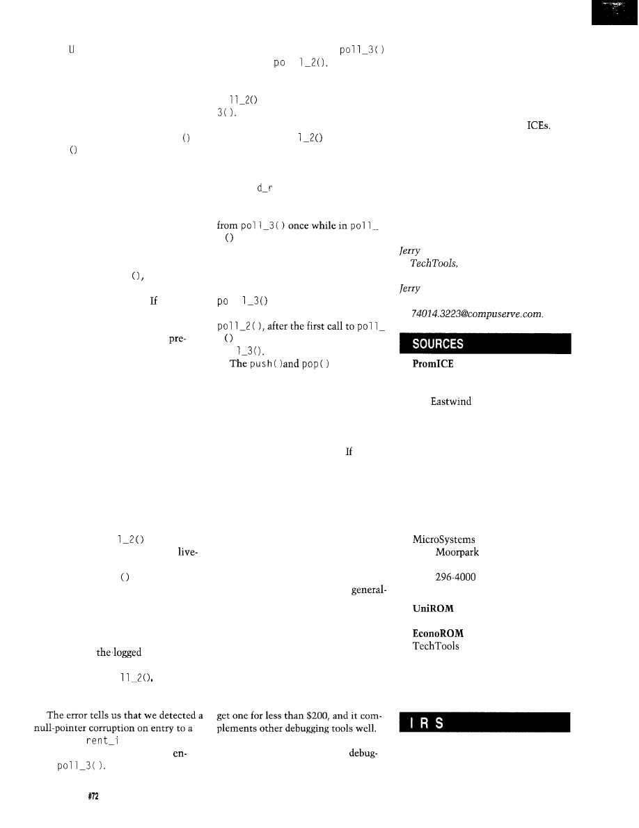
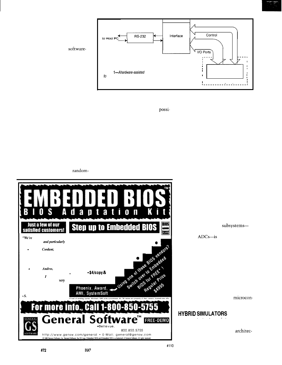
Footprint Connector
Figure
simulator uses hardware
Plugged into
An important advantage of simula-
provide
the electrical interface between the real world
Microcontroller Socket
tion is that debugging is not dependent
and a software simulation of the microcontroller, but cannot
perform MO at real-time speeds.
User’s Target System
on the availability of target system
hardware. This advantage enables
software to be well developed long
number generator (RNG) routine or
To offset this limitation, some
before prototype hardware is available.
implementation of a DSP algorithm.
simulators construct stimulus files.
It also enables several members of a
In these cases, the additional
These files synchronize changes in
development team to work in parallel
bility of using the general-purpose
input conditions as the simulation
on different parts of a project where
computer to create test input data (e.g.,
executes, generating log files to record
only a single target hardware platform
is available for reasons of cost, bulk, or
accessibility.
Simulation is especially useful in
developing small, self-contained soft-
ware components not highly depen-
dent on the target system’s specific
hardware configuration. Typical ex-
amples are development of a
to evaluate the performance of a digital
filter) or to analyze the output data
(e.g., to determine the randomness of
the RNG) may be a real bonus.
The major problem with simulation
as a debugging tool is that, by its very
nature, it is divorced from the real
world. It cannot readily be coupled
with the taget system’s hardware.
impressed by the level of
documentation
by the readability of the code”
M. Ryan,
Inc.
“Fast,
flexible, high-quality
code, and excellent
technical support.”
L. Allen,
Inc.
‘Personally, found the
Adaptation Kit and tool set
straightforward to use, making
the BIOS development
process relatively easy.”
Chaplin, Software Engineer.
Includes our award-winning Run-From-Rom DOS
Includes Flash Disk for popular Flash parts
l
Over 300 easy configuration options
BIOS Kit includes full source code
l
Royalties
down
l
the states of the simulated outputs and
other conditions.
In simple situations, this is suffi-
cient. But, it’s largely useless when
outputs can directly or indirectly affect
inputs (e.g., when developing a driver
to write and verify flash memory or
routines to support CAN-bus network
communications in automotive appli-
cations). In these cases, it’s generally
impossible to sufficiently simulate the
external hardware environment.
This problem extends to the periph-
eral hardware resources of the micro-
controller itself. Simulators are often
limited to the basic instruction set,
core registers, and internal memory of
the target microcontroller.
Simulation of other
like timers, communications inter-
faces, and
generally not
supported. Many also ignore timing
issues greatly limiting their usefulness
in time-critical applications like en-
gine management or AC-induction
motor control.
In the past, speed of execution sig-
nificantly limited the usefulness of
software-based simulators, but this is
no longer necessarily the case. On a
Pentium PC, you can simulate the
core instruction set of many
trollers faster than the real device.
Some limitations of simulators
3 2 0
1 0 8 t h A v e . N . E . , S u i t e 4 0 0
W A 9 8 0 0 4
interfacing with real-world hardware
T e l : 2 0 6 . 4 5 4 . 5 7 5 5 . F a x : 2 0 6 . 4 5 4 . 5 7 4 4 . S a l e s :
can be overcome with hybrid
ture. Here, the software simulator
28
Issue
July 1996
Circuit Cellar
combines with a hardware input and
output interface unit, which plugs into
the target hardware system in place of
the microcontroller to be emulated
(see Figure
1).
Communication between the host
computer and the interface unit takes
place via a standard serial or parallel
port or a custom interface board in an
expansion slot.
The control program to be debugged
executes more or less entirely within
the simulator on the host computer.
The interface mainly provides the I/O
pins of the emulated device. To ensure
that the electrical characteristics of
the emulated microcontroller closely
match those of the real device, the
interface unit is usually based on a
microcontroller from the same family
as the emulated device.
The interface microcontroller con-
tains firmware that communicates
with the host PC and executes I/O
functions difficult or inefficient to
simulate, such as analog-to-digital
conversion, PWM waveform genera-
tion, and serial communications.
Although some peripheral hardware
resources are successfully emulated
with this hybrid approach, it doesn’t
work for all subsystems and functions.
It’s less than satisfactory for real-time
I/O-intensive applications, such as
timers (especially those with real-time
capture and compare functions) and
subsystems with interrupts.
Also, a hybrid simulator using a
serial communications link to the host
computer often steals the communica-
tion-interface hardware resources of
the target microcontroller. So, it’s
difficult to debug a
oriented application.
A second problem with hybrid sim-
ulators is execution speed. While a lot
of the core instruction set is simulated
at real-time speeds, as soon as an in-
struction requires an I/O operation,
speed dramatically reduces. The neces-
sary communications transactions
between the simulation program and
the interface unit slow the simulator
significantly.
Because they require no special
hardware, simulators are traditionally
one of the lowest-cost debugging tools.
In the circumstances described above,
and educational roles, simulators are
very useful. Hence, they represent
good value for the money.
Many vendors of more expensive
hardware-based debugging tools recog-
nize the special place of simulators.
They often provide a means to use the
software component of their products
in a simulation mode.
But, it’s less certain whether the
improvements offered by hybrid simu-
lators are worth the extra expense of
the special interface hardware.
ROM EMULATORS
A ROM emulator is effectively a
dual-port memory device. You see in
Figure 2 that the target microcontrol-
ler has read access to the memory
contents via one port and a host com-
puter has write access via the other.
The host computer connects to the
ROM emulator with a standard serial
or parallel interface. It typically down-
loads program code for debugging in a
few seconds. The ROM emulator nor-
* Easy to use schematic entry program
for circuit diagrams,
only $149. Includes netlisting, bill of materials, extensive parts libraries.
l
Powerful, event-driven digital simulator
allows you
to check
logic circuitry quickly before actually wiring it up. Works directly within
the
editor from a
menu and displays results in “logic
analyzer” display window. Starting at $149 this is the lowest cost
simulator on the market. Library parts include TTL, and
devices.
l
Analog simulator
for $149. Allows AC, DC and transient
circuit analysis. Includes models of transistors,
and op amps.
l
Circuit board artwork editor and autorouter programs
starting at $149. Produce high quality artwork directly on dot matrix or
laser printers. You can do boards up to 16 layers including surface mount.
Includes Gerber and Excellon file output. Autorouter accepts
and
placement data directly from the
schematic editor.
l
Low cost combination packages with schematics and PCB design: 2-layer
for
for $649.
Write or call for free demo disks:
MENTAL
5415 136th Place S.E.
WA 98006
(206) 641-2141
l
BBS (206) 641-2846
Internet:
ADC
l
DAC
A-channel,
ADC
Frequency input: directly reads 2 Hz to 2
PWM output: 2 Hz to 3.5
5-95% duty cycle
High-performance, built-in functions: parallel
buffering, LCD and keypad control, analog data averaging
RS-422, and RS-485 at 300 bps to 115 kbps
Eight parallel in/eight parallel out lines and
bus
Simple
ASCII command set, requires no programming!
Sixteen-character ID allows hundreds of Net-Ports
Small size, encapsulated construction
30
Issue
July 1996
Circuit Cellar INK@
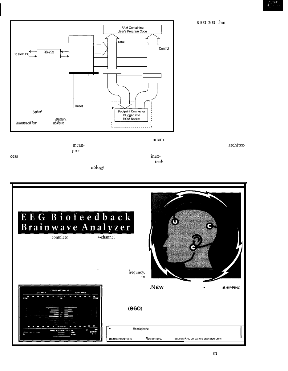
Serial Interface
ROM Emulator
System
Microcontroller
Address,
First, ROM emulators require
the target to fetch its control pro-
gram from an external memory
device.
Some microcontrollers operate
in a single-chip mode, where the
Buffer Control
Buffer
Buffer
program and data memory is inter-
nal to the device itself and the
majority of the device pins are
available for I/O.
Others operate in an externally
expanded mode. These emulators
interface to external program and/
Figure 2-A
ROM emulator can
on/y
be used where a microcontroller
or data memory where a substan-
executes code
from external
tial number of the device pins
cost for the
control and monitor execution.
User’s Target System
must be dedicated to providing the
necessary data, address, and con-
trol interface.
mally controls the microcontroller’s
memory device from which the
If your target system is designed
reset pin to prevent it executing
controller fetches its control program
using an externally expanded
ingless code until the download
instructions. ROM emulators are
ture, it’s no problem. But, a ROM
is complete.
therefore simple and relatively
emulator is of little or no use if your
Rather than emulating the whole
pensive-modern manufacturing
design requires the microcontroller to
microcontroller in the target system,
produces ROM emulators no
operate in single-chip mode in order to
the ROM emulator just emulates the
larger than standard memory devices
provide the number of I/O pins you
that cost
the sav-
ings is achieved at the expense of
two major shortcomings.
H A L - 4
The HAL-4 kit is a
battery-operated
electroenceph-
alograph (EEG) which measures a mere 6” x 7”. HAL is sensitive enough
to even distinguish different conscious states-between concentrated
mental activity and pleasant daydreaming. HAL gathers all relevent alpha,
beta, and theta brainwave signals within the range of 4-20 Hz and presents
it in a serial digitized format that can be easily recorded or analyzed. HAL’s
operation is straightforward. It samples four channels of analog brainwave
data 64 times per second and transmits this digitized data serially to a PC
at 4800 bps. There, using a Fast Fourier Transform to determine
amplitude, and phase components, the results are graphically displayed
real time for each side of the brain.
HAL-4
K I T . . . . .
P
A C K A G E
P
R I C E
$ 2 7 9
Contains HAL-4 PCB and all circuit components, source code on PC diskette,
serial connection cable, and four extra sets of disposable electrodes.
to order the HAL-4 Kit or to receive a catalog,
C A L L :
875-2751 OR FAX:
( 8 6 0 ) 8 7 2 - 2 2 0 4
C
I R C U I T
C
E L L A R
K
I T S
l
S
UITE
12
l
V
E R N O N
4
P
A R K
S
T R E E
l
C T 0 6 0 6 6
T
The Circuit Cellar
Activation Level detector is presented as an engineering example of
the design techniques used in acquiring brainwave signals. This Hemispheric Activation Level detector is
not a medically approved device, no medical claims are made for this device, and it should not be used for
purposes.
safe use
Circuit Cellar INK@
Issue
July 1996
31
need. It also won’t help if your micro-
controller doesn’t support external
expansion (typical of low-end devices
in packages of fewer than pins).
In a target system where a micro-
controller is in single-chip mode and
supports external expansion, you
might temporarily do without the I/O
pins that interface external memory
(the ROM emulator) while debugging.
However, this is inconvenient at best.
Some manufacturers produce spe-
cial development devices with a socket
for a memory device containing the
control program piggybacked onto the
package. But, these devices are rela-
tively uncommon and may cost as
much as the ROM emulator itself.
The second major shortcoming of
emulators is that they only provide a
means to submit program code to the
microcontroller for execution. Control
is limited to holding the microcontrol-
ler reset during the download pro-
cess-something your target system
must tolerate without upsetting ancil-
lary subsystems-and then releasing it
on completion. Execution then begins
from the standard reset point.
From then on, you cannot influence
the program’s operation or monitor its
activity. The emulator has only sped
up the process of program submission
(which might otherwise require a te-
dious burn-test-erase sequence using
erasable EPROM devices).
Some vendors attempt to offset this
shortcoming by including additional
memory capacity in parallel with that
required for the control program. With
companion software on the host com-
puter, flags are set in that memory for
ranges of program addresses, which
can in turn trigger an oscilloscope or
other item of test equipment. You can
then determine whether a particular
portion of a program is being executed,
verify order of execution, and time the
execution duration.
Some vendors have added
analyzer-type hardware. This hardware
monitors and records program ad-
dresses and other external logic states
as instructions are fetched. It displays
execution traces and profiles.
Of course, these features inflate
price and bring the ROM emulator
into competition with the other more
capable emulation tools discussed in
subsequent sections of this article.
Recent advances in microcontroller
fabrication technologies have in some
cases rendered the ROM-emulator
concept irrelevant. Some microcon-
troller devices now have internal pro-
gram memory implemented using
electrically erasable nonvolatile mem-
ory technologies (e.g., flash memory).
Code downloads directly into the de-
vice in situ in the target.
ROM emulators undoubtedly have
a place in some applications, but they
are better suited to traditional
CONNECTS TO RS-232)
chip architectures than single-chip
AR-16 RELAY INTERFACE (16 channel) . . . .
Two 8 channel
level) outputs are provided for
microcontrollers. Apart from low cost,
connection to relay cards or other devices
lo 128
their other advantages include:
relays car
s using EX-16 expansion cards). A
of
sand relays are stocked. Call for more in
l
universality-they can be used with
any externally expandable
AR-2 RELAY INTERFACE (2 relays, 10
RO-6 REED RELAY CARD (6 relays, 10 VA) . . . . . $49.96
RN-6 RELAY CARD (10 amp SPDT, 277
A N A L O G
controller or replace a ROM device
D I G I T A L
l
ability to be ganged for wide-memory
systems
l
high speed and large capacity-units
with megabytes of memory and
access times in the few tens of
nanoseconds are readily available
l
minimal power requirements-nor-
mally power can be derived from
the target system
Next month, we’ll discuss more
sophisticated tools including
based debuggers and true in-circuit
emulators.
q
Graham Moss is a design engineer
with the applications laboratory of
Philips New Zealand, which designs
and markets a variety of low-cost
development tools for microcontrol-
lers. He may be reached at graham8
The laboratory’s web site is
at
(CO
NNE
C
T
S
CONVERTER’ (16
CONVERTER* channel/IO
Input voltage. amperage,
light,
and a wide variety of other types of analog
available (lengths to
for info on other
configurations and 12
(terminal block and cable sold separately).
Data Acquisition
for Windows or 3.1
TEMPERATURE INTERFACE* (6
term. block 8 temp. sensors
to 146’ F).
INTERFACE’ (6
channel) . . . . . . . . . $99.96
status of relays, switches, HVAC equipment,
devices, keypads, and other devices.
PORT SELECTOR (4
channels
an
port into 4 selectable RS-422
to RS-422 converter) . . . . . . . . . . . . . . . . . . .
your interface to control and
up lo 512 relays, up to 576 digital inputs, up to
ST-32 8 AD-16
cards.
inputs or up to 128 temperature inputs using
TECHNICAL
over the
our staff. Technical reference
Ross
and Ken Mardle are
design engineers with Applied Digital
Research, a New Zealand company
specializing in embedded systems and
development tools. You may reach
Ross and Ken at
software pro rammin exam
GW Basic, Visua
it
Turbo C. Assembly and others are provided.
l
for continuous 24
hour
industrial
10 years of
performance in e energy management field.
*CONNECTS TO RS-232, RS-422 or
with
and compatibles, Mac and most computers. All
standard baud rates and protocols (50 to 19,200 baud).
our
number.
or E-mail to order. or visit our Internet on-line
Technical
404
Very Useful
405
Moderately Useful
406 Not Useful
UR
E-mail:
(614)
technical support
ENERGY CONTROL, INC.
Suite
Columbus,
43215-5491
Circuit Cellar
INK@
Issue
July 1996
33
Jim Sibigtroth
A Single-Wire
Development Interface
new
are
introduced, some
methods are running
into big problems. Pin counts are going
up, so emulators that clip over or re-
place the main MCU are becoming
more mechanically unmanageable
and/or ridiculously expensive.
Before getting into the details, let’s
look at the whole system-from the
PC to the target system under develop-
ment. As shown in Figure 1, an inter-
face pod acts as a translator between
your terminal or PC and the target
application system. The pod serves
two main purposes.
Higher bus speeds are very difficult
to emulate through an umbilical.
Single-chip
with large
memory systems don’t even have ex-
ternal address and data buses, so logic
analyzers and ROM-replacement ap-
proaches don’t always work.
First, the pod contains firmware to
talk to the custom serial protocol of
the
single background
interface pin (
BKGD
).
Serial background debugging can
overcome these problems. In “No
Emulator? Try a One-wire Debugger”
(INK
Hank Wallace shows the
need for a one-wire debugger and does
a good job of using the materials at
hand in a small system.
Second, the pod includes a monitor
or ASCII command interpreter so the
terminal or PC can issue commands to
the target system and retrieve data
from it.
A small piece of code was embed-
ded into the application program to
send desired debug information out on
a single output pin. A very simple
connection to a PC parallel port and
software in the PC monitored this
debug information.
The wiring is a simple RS-232 con-
nection between the host PC and the
pod and a
cable between
the pod and the target system. Al-
though only BKGD on the target MCU
is used for communication, you still
need a common ground connection.
The optional third wire connects to
the target system Reset. This feature
isn’t absolutely necessary, but it pro-
vides a nice way to remotely reset the
target system from your PC keyboard.
While this approach is great for
The fourth wire can steal
getting you out of a jam, it’s better if
power from the target system for the
you don’t need to add the code in the
pod. If your application power supply
application system or share the output
can handle a few extra milliamps,
pin.
doing this is more convenient than
It’s even better if the debug link is
bidirectional, so you can interactively
debug the target application.
Enter the new single-wire back-
ground debug mode (BDM) interface on
Motorola’s newest family of
Unlike previous background systems,
the
uses a single dedicated
pin and no target-system resources.
Target-system memory can be read
from and written to while the target
application is running, without affect-
ing real-time operation. The applica-
tion system and the debug interface
are completely independent.
The system understands a complete
set of primitive debug commands from
memory modify to single-instruction
trace. Everything you expect in the
debug monitor of an emulation board
can be implemented with this
wire interface.
BIRD’S EYE VIEW
34
Issue
July
1996
Circuit Cellar INK@
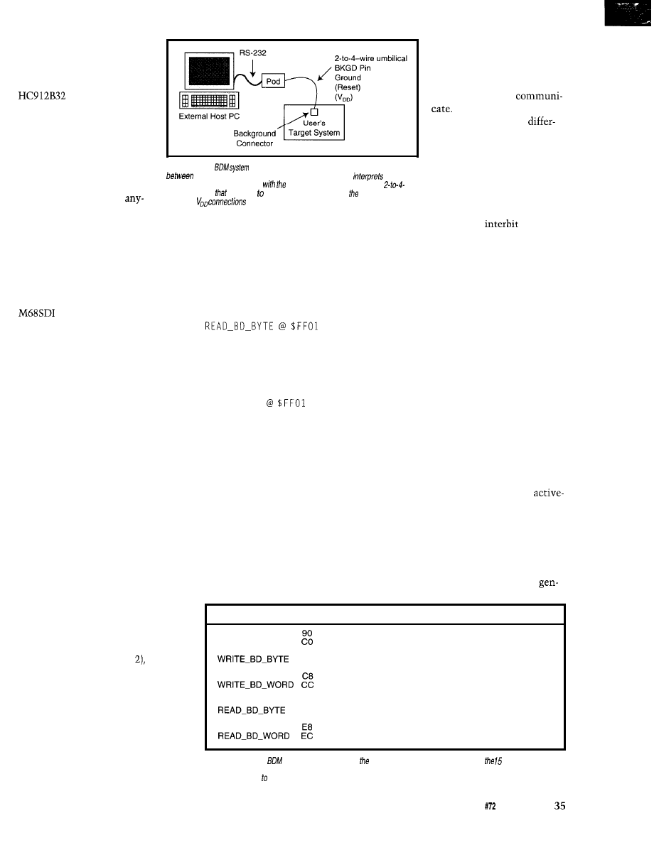
providing a separate power
The external master must
source for the pod.
either be told what this speed
Typically, the pod contains
is by the user, or the master
an MCU such as the MC68
must determine the target
and an RS-232-level
speed before it can
translator chip. The ‘HC 12’s
Each bit time is 16 bus
‘B32 version has 32 KB of flash
clocks long. Ones are
and 1 KB of RAM, so there’s
entiated from zeros by the
plenty of room for a complete
length of time the BKGD pin
debug monitor similar to the
is held low.
Buffalo monitor for the ‘HC
11.
Figure 1-A
can use
a
standard RS-232 link to
communicate
a host PC and the debug pod. Firmware in fhe pod
host
The time between bits is
With a full monitor in the
commands and communicates
user’s target system through a
arbitrary because the external
pod, the host PC can be
wire
umbilical
connects a background connector on fargef system. The
reset and
are nice but not required.
host and the target MCU are
thing that can run a simple
terminal emulator. You don’t have
need a fancy debugger for your PC.
If you want to interface a commer-
cial debugger program with a nice
GUI, the pod implements a standard
set of serial debug server commands
instead of the monitor program. The
is an example of a pod with
standard server commands. It’s more
user-friendly, but it costs more and
ties you to a specific host such as a
Windows-compatible PC.
THE BDM COMMAND SET
The ‘HC12 background system
understands a set of primitive com-
mands which consists of 24 commands
divided into two groups.
The hardware commands listed in
Table 1 are implemented in dedicated
logic and can be executed without
disturbing the running application
program. BDM logic looks for cycles
where the CPU is not using the buses,
so there’s no real-time impact on the
running program.
The second group of commands
can’t be done while the application
program is running, like modifying
CPU registers or tracing one instruc-
tion. Since the CPU is not executing
user instructions at this time, it’s
available for use by the background
debug system. Commands in this sec-
ond group (listed in Table are called
firmware
commands
because they are
implemented in a small BDM ROM.
To execute firmware commands,
the application program is stopped and
the MCU enters the active background
mode. While BDM is active, a small
BDM ROM is in the MCU memory
map as well as a few BDM storage and
control registers. These resources
aren’t visible when the user applica-
tion is running, so they don’t interfere
with the application system.
The hardware commands include
separate commands for accessing user
memory and the BDM resources which
occupy some of the same addresses.
For instance, the BDM command
returnsthe
same value in the BDM status register
as is in the BDM memory map.
This BDM status register is not
visible in the application program’s
memory map. The BDM command
READ-BYTE
returnsavalue
from the user’s program memory.
SINGLE-WIRE COMMUNICATION PIN
To fit relatively high-speed bidirec-
tional communication onto a single
pin, a custom protocol was developed.
To avoid a separate pin for a clock
signal, the protocol designates the
external host as the master.
All bit times are initiated when the
external host drives a falling edge on
the BKGD pin. Timing is controlled by
the speed of the bus-rate clock in the
target MCU.
asynchronous to each other.
There is a maximum
delay,
after which the MCU resets its BDM
logic and starts looking for the first bit
of a new command.
If the communication link ever gets
out of synchronization, the host can
simply stop driving the BKGD pin for
at least 5
12
target bus clocks to force
this time-out.
Usually the external host is the
device that drives the BKGD pin. But,
when the host requests data from the
target MCU, the target MCU also
needs to drive this pin. The pin is
designed as a pseudo-open-drain driver.
When there’s an unintended conflict,
both the host and the target MCU
drive the pin low, which avoids any
electrical harm.
Normal open-drain pins tend to be
slow due to R-C rise time, so this sys-
tem is modified to provide brief
high pulses to speed up the rise times.
This design modification allows much
faster communication than you’d nor-
mally expect to get from an open-drain
pin.
When communication is from the
host to the target MCU, the host
Opcode Operands
BACKGROUND
WRITE-BYTE
ah al ee xx (even)
ah al xxoo (odd)
C 4
ah al ee xx (even)
ah al xx oo (odd).
WRITE-WORD
ah al ee oo
ah al ee oo
READ-BYTE
EO
ah al ee xx (even)
ah al xx oo (odd)
E 4
ah al ee xx (even)
ah al xx oo (odd)’
READ-WORD
ah al ee oo
ah al ee oo
Description
Enter active BDM if firmware enabled
Write a byte of data to user memory
Write a byte of data with BDM in map
Write a word of data to user memory
Write a word of data with BDM in map
Read a byte of data from user memory
Read a byte of data with BDM in map
Read a word of data from user memory
Read a word of data with BDM in map
Table l--The
instruction set consists of 9 hardware commands given here and firmware commands
shown in Table 2. Hardware commands may be executed without disturbing a running user program. A hardware
command is used set the firmware-enable bit.
Circuit Cellar INK@
Issue
July 1996
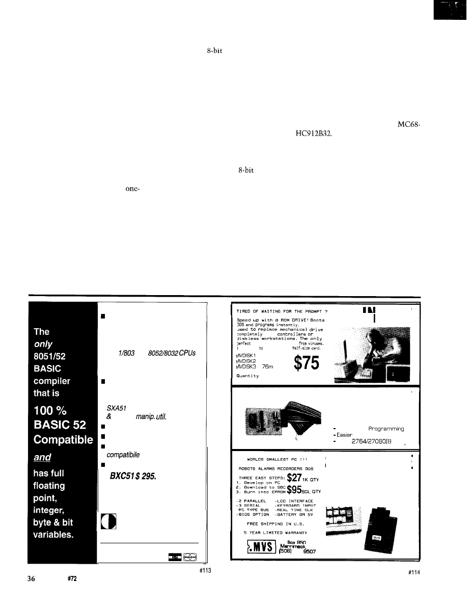
erates brief speed-up pulses at the end
of each driven-low period.
It’s a little more complicated when
the target is sending return data to the
host as shown in Figure 2. In that case,
the host initiates the bit time by driv-
ing BKGD low just long enough for the
target to recognize the falling edge.
Next, the target either reinforces
the low, holding it for 12 cycles (for a
logic zero), or allows the pin to rise (for
a logic one).
In the case of the logic zero, the
target drives the brief high speed-up
pulse as soon as it releases its low
drive to the pin.
For a logic one, the target waits for
seven cycles and then drives a
cycle-high speed-up pulse.
Timing is a little tricky. The special
pulse comes after the host stops driv-
ing the low-bit-start pulse and before it
samples the bit level at about cycle
nine. The timing variation is due to
the uncertainty of when the ‘HC12
sees the falling edge at the start of the
bit compared to when the host gener-
ates the edge.
Commands, addresses, and data are
transferred MSB first. Each command
starts with an
command word
from the external host to the target
MCU. Some commands nothing else.
Hardware commands that read or
write memory require a 16-bit address
after the command to identify the
location in the target system to be
accessed. If the command is a memory
access, a 16-bit data word is sent to
[writes) or received from (reads) the
target after the address.
Data is always 16 bits to simplify
the logic in the target MCU. When the
command calls for only
data, the
host is responsible for getting it to or
from the correct half of the 16-bit data
word, and the other half of the data
word has a “don’t care” status.
LET’S DO SOME WORK
Let’s be very optimistic and assume
you never have bugs, so you don’t need
to debug anything. This system is still
useful in the manufacturing process.
You can build your whole system
using unprogrammed flash memory.
After final assembly, you can connect
the pod and download your application
software into the target system from
your PC. This feature gives you more
time to develop and test your code
before committing to production.
The background system can access
anything the target CPU can, so the
nonvolatile program memory can be
an external memory or an on-chip
flash like the 32-KB flash in the
The background debug mode can
also be used for system calibration.
Imagine that your system has a sensor
component that varies from one sys-
tem to another. A correction factor
stored in nonvolatile memory can
compensate for the variations in sen-
sors.
Rather than including a calibration
program in your application code, you
can monitor the operation of the sen-
sor through serial debug commands.
Next, you can program the calibration
adjustment factors into the nonvolatile
memory using other serial background
commands.
Memory mapped variables
n
In-line assembly language
option
n
Compile time switch to select
805
1 or
n
Compatible with any RAM
or ROM memory mapping
Runs up to 50 times faster than
the MCS BASIC-52 interpreter.
n
Includes Binary Technology’s
cross-assembler
hex file
Extensive documentation
Tutorial included
Runs on IBM-PC/XT or
Compatible with all 8051 variants
n
508-369-9556
FAX 508-369-9549
Binary Technology, Inc.
P.O. Box 541
l
Carlisle, MA 01741
Issue
July 1996
Circuit Cellar INK@
ROM!
DOS’in
Also
in
protection
Easy install
128k
$ 7 5
1 4 4 m $ 1 5 0
5
5 1 9 5
discounts!
$95 EPROM
PROGRAMMER
Super Fast
to use than others
Does
M e g ]
NH
792
8088 SINGLE
BOARD
COMPUTER
Have you ever noticed
how your auto-service deal-
er connects the service
computer to a connector on
your car and reads out in-
formation about recent
system failures? This capa-
bility is supported by extra
software in an embedded
body-control processor.
The presence of the
service computer enables
software to respond to re-
quests for service informa-
tion. This capability im-
plies that all the questions
the service computer can
ask were agreed on before
the car was built.
Command
Opcode
Mnemonic
(hex) Operands Description
W R I T E - N E X T 4 2
dh
X=X+2; Write word to 0,X
WRITE-PC
dh
Write user program counter
WRITE-D
dh
Write user D accumulator
WRITE-X
45
dh dl
Write user index register X
dh dl
Write user index register Y
dh dl
Write user stack pointer
READ-NEXT
dh dl
X=X+2; Read word from 0,X
READ-PC
dh dl
Read user program counter
dh dl
Read user D accumulator
dh dl
Read user index register X
66
dh dl
Read user index register Y
dh dl
GO
Read user stack pointer
Resume user program at
current PC location
TRACE1
10
Trace 1 user instruction and
return to active
18
Enable instruction tagging
and resume user program
at current PC location
to
run it. Some bug causes
the program to fail.
If you’re relying on a
debugging routine in the
application code to tell you
what’s going on, you may be
out of luck because the
bug(s) may cause this code
to run incorrectly or not at
all. In this environment, the
code has to be almost work-
ing before you can use the
debug routines.
Table
firmware commands in the
instruction
they must
be enabled and
must be active (user program stopped).
Now, imagine what you could do if
the service connector was the single-
wire background connector.
This approach leaves a little more
processor bandwidth for the actual
application. It also relieves the applica-
tion programmer from writing the
communication routines.
With this new single-
wire BDM, you connect the
debug pod to the target
system. Depending on how
serious the bug is, you can
try to start talking to the
target without resetting it to see what
it
is
doing (instead of what it should be
doing).
The embedded body controller still
needs to record system failures in
memory somewhere. But, you no
longer need special routines to handle
communication through the service
connector.
Now, let’s be more realistic and
talk about debugging programs that
don’t quite work on the first try. You
load the code into your system and try
If things are really bad, you force a
reset and startup with the background
mode active. (Don’t run the user pro-
gram.)
From here, you set the program
counter to the start of the user
P
Odds are that some time during the day you
will stop for a traffic signal, look at a message
display or listen to a recorded announcement
controlled by a Micromint
We’ve
shipped thousands of
to
Check out why they chose the
by
calling us for a data sheet and price list now.
MICROMINT, INC.
4
Park Street, Vernon, CT 06066
(860)
(860) 872-2204
in Europe: (44)
Canada: (514)
Inquiries Welcome
Circuit Cellar INK@
Issue
July 1996
37
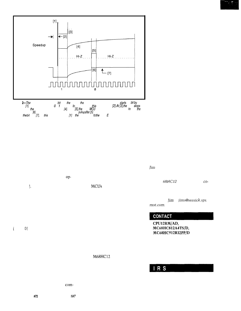
Host Drive
Bit Start Pulse
-
L
Rise Time
If No
-
L
Target Drives
Speed-up Pulse
H i - Z
BKGD Pin
Target ECLK
for reference
2
3
4
5
6
7
9 10 11 12 13 14 15 16
One Logic 1 -bit Time-Host Reading from Target
gram and trace single instructions,
checking the state of registers and
memory between steps to see if every-
If this is too slow or if you are sure
that certain parts of the program are
thing has the expected values.
okay, you can set a breakpoint after
the known-good code and single-step
the parts you are unsure about.
In previous systems, debuggers
established breakpoints in application
code by replacing an instruction
code with the code for a software inter-
rupt (SW I The service routine for SW I
would be a call to the debug monitor.
This method was intrusive because
it interfered with any other use of the
SW
I
by the application program. It also
involved the addition of SW I service
code for the debugger in the applica-
tion program.
In the ‘HC
12,
the background
B
G N instruction opcode can be used
instead of SW
I.
Since this opcode isn’t
used in normal application programs,
it isn’t intrusive.
The code that is executed to service
the B G N D instruction is in the BDM
ROM, which is not part of the normal
user map. So, it doesn’t take up any
space in the user’s program memory.
THE FUTURE OF DEBUGGING
The debug capabilities offered by
this new single-wire system are
38
Issue
July 1996
Circuit Cellar
Figure
host reading a logic one from fargef is most complex case. The hosf
fhe
driving low The target fakes from fo bus cycles synchronize fo
falling edge
host
driving low and pin begins a slow R-C rise
At
fargef
drives a high speed-up pulse snap
pin to a logic one This high is held by a weak external
stops driving. A short time later, the host
samples level but
is referenced
fo in host and not fargef clock.
The background debug pod requires
parable to those you get in a full-fea-
only two to four connections to the
target system-and that’s reasonable,
tured emulator. However, in this sys-
even in the tightest applications. No
debug code needs to be incorporated
tem, the actual target MCU is not
into the application program. The
designer is free to work on the applica-
replaced by an emulator.
tion instead of devising debugging
routines.
As
get more complex and
packages get smaller, traditional paral-
lel emulation techniques become less
practical. Prior to serial background
systems, most development ap-
proaches required access to address
and data bus information.
The availability of large on-chip
flash memory makes expanded mode
systems less common. The need for
serial debug systems like this one
increases. Some new versions of the
‘HC12 even include on-chip logic for
hardware breakpoints, which simpli-
fies debugging programs in flash.
The
family represents
another step in the evolution of serial
background debug systems. Compared
to previous serial background systems,
the ‘HC12 has fewer connections and
accesses memory while the application
runs in real time. The logic and re-
sources for this system are separate
and hidden from the normal applica-
tion. They don’t interfere with the real
application.
Debugging microprocessor systems
has evolved as these systems have
become more sophisticated. Origi-
nally, few tools other than logic probes
and oscilloscopes were available. Logic
analyzers and in-circuit emulators
were developed, but they require a lot
of target-system connections.
Embedded systems continue to
develop with faster clock speeds and
higher-pin-count packages. To keep
up, emulators and logic analyzers have
become more sophisticated, and the
connection systems have become more
unmanageable.
Most of these tools are out of reach
for a typical experimenter. While serial
debuggers don’t completely replace
traditional parallel systems, they offer
good debug capabilities, while elimi-
nating some of the problems.
The simple serial connection elimi-
nates a costly umbilical and is not
required to operate at submicrosecond
speeds. For low-cost debug, this new
breed of serial debugger is the obvious
choice.
q
Sib&troth is a system design engi-
neer working on advanced microcon-
trollers for Motorola. His latest project
was the
where he was a
architect
for the CPU12 instruction
set. He devised the background debug
system described in this article. You
may reach
at
Motorola Literature Center
P.O. Box 13026
Austin, TX 78711
(800) 7657795, Ext. 950
Fax: (800) 7659753
407
Very Useful
408 Moderately Useful
409 Not Useful
Designing
with Flash
Memory
Arvind
won’t be able to
use flash memory-whether you like it
or not. It’s a simple matter of econom-
ics.
Unless you have some legacy appli-
cation and the government is paying
you to buy the parts, you’ll pick and
use flash memory wherever you were
using ROM before.
These days, flash often simply re-
places the ROM. In this article, how-
ever, I’ll be talking about using flash in
its full functionality.
WHAT IS FLASH MEMORY
Flash is nonvolatile, erasable,
able, low-power, high-density,
state memory in a chip. It’s a ROM,
it’s a RAM, it’s a solid-state disk. But,
it’s smaller, denser, and less
hungry than just about all of them.
However, the similarities stop there.
The ROM, RAM, and disk drives have
been around a long time. We know
how to design with them, how to use
them, and what their capabilities and
limitations are.
None of these things are true for
flash. Flash has gone through a lot of
evolutionary change.
Flash devices have a certain pecu-
liarity. Although they’re writable, you
must remember they don’t operate like
RAM. You may write bytes of data to
the memory locations in the device,
but to rewrite any data, you must first
erase either the entire chip or the par-
ticular sector.
Also, when processing, the device is
unavailable for all but status-read
operations.
WHY FLASH
In deciding whether or not you
should use flash, the relevant ques-
tions are:
l
will flash devices make your prod-
ucts better, cheaper, and more com-
petitive?
l
will flash devices enable you to make
products you couldn’t make before?
l
what are its real advantages?
l
how can you exploit flash now that
it’s here?
l
how are others taking advantage of
flash and what are they doing with
it?
When you see what flash is and how it
works, you’ll arrive at the answers
relevant to your situation.
USES OF FLASH
The potential use of anything is
unlimited. It’s up to the user’s imagi-
nation. But, there are things that flash
is quite suitable for. Some of these
innovations have yielded significant
advantages.
For example, there are clear advan-
tages to storing the firmware for a
product in flash. Unlike ROM, flash is
programmable in-circuit. The software
can be updated in the field and cus-
tomized to user needs on demand.
Flash is quite fast. Software can run
at full speed directly from flash. One
popular application in this area is BIOS
storage. BIOS no longer has to be cast
in stone.
Systems may need the BIOS up-
dated to accommodate processor up-
grades, support for newer graphics
devices, power-management features,
fixing of bugs, improvements in opera-
tion, or support for plug-in PCMCIA
devices. In hand-held and portable
systems, or in systems that are diffi-
cult or impossible to disassemble,
flash nonetheless provides software
upgrades.
For hand-held measuring devices or
remote sensing and measuring devices,
flash offers something not easily at-
tainable before: nonbattery-powered,
nonvolatile memory.
Flash reliably stores information.
You don’t have to worry about it being
lost because the backup battery died.
40
Issue July 1996
Circuit Cellar INK@
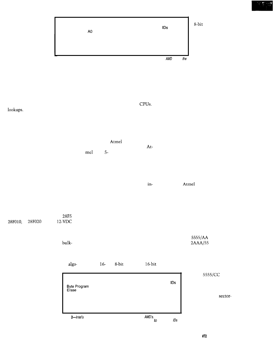
It’s also more immune
to shock and tempera-
ture-related changes.
And, it offers much
higher density than
other available tech-
nologies (e.g., SRAM or
Read Reset
FO restores flash device to read mode
Auto Select
90 allows reading of manufacturer and device
Byte Program
programs a single byte
Erase
80 requires double-unlock sequence for chip or sector erase
Chip Erase
10 erases entire chip minus the protected sectors
Sector Erase
30 erases one or more sectors, won’t erase protected ones
Erase Suspend
BO temporarily suspends sector-erase operation
Erase Resume
30 resumes sector-erase process immediately
EEPROM).
Storing large
SOFTWARE
, DESIGN ISSUES
Table
l-By embedding low-level write and erase algorithms inside the f/ash device,
enables
developer to execute previously
complicated f/ash functions by issuing a simple command.
Of the two possible
ones being usable in
mode. I expect
these to proliferate in
embedded applica-
tions.
amounts of data for
ways to
program a
lookup tables (e.g., a phone-switching
application) enables the service pro-
vider to customize and store customer
preferences. Other applications such as
printer fonts, phone numbers in por-
table phones, address information in
your PDA, and so on also need quick
components and synchronous- and
DRAM-interface flash-memory com-
ponents are intended for PCMCIA and
desktop or portable computing applica-
tions. In these applications, the
DRAM-like interface allows easy inte-
gration of flash with existing
flash, the first is to program it before it
is installed in the target system. You’d
use a device programmer (i.e., a ROM
programmer) that can also program
flash devices.
Last but not least, flash memory is
popularly used as a file system. Many
custom and off-the-shelf flash file
systems are available. These systems
enable you to use flash memory as a
solid-state disk.
However, the most interesting and
popular components for embedded
applications are the boot-block compo-
nents offered by Intel and AMD. Intel
parts are second-sourced by several
other manufacturers.
This way, the flash is programmed
beforehand, and sectors are protected
by applying the higher voltages needed
for such tasks. This method is com-
mon when the flash replaces ROM in
an existing application or when you’re
placing boot code in a protected block.
Flash is blindingly fast and compact
for the amount of storage it offers. It
gives more convenience, more reliabil-
ity, and lower power than a magnetic
spinning medium. Very small and light
portable computers obtain storage
capability matching the much heavier
and power-hungry portables of yester-
day.
AMD and
offer additional
simple sector-erase components.
offers and 3-V devices in densi-
ties of 32-5 12 KB. Their numerous,
smaller sectors make them attractive
alternatives to big parts from Intel and
AMD, which generally offer parts from
1 Mb and up.
The second method is to program
the flash in-circuit after the part has
been soldered down or socketed. You
accomplish this by issuing commands
to the flash device with proper soft-
ware algorithms.
These parts are programmable
circuit using only 5 V. Some operate at
only 3 V.
Unfortunately, more than one type
of algorithm is needed for the different
vendors’ parts. The algorithms used by
AMD and
parts go back to the
days of the EEPROM, which is what
flash really is.
HARDWARE DESIGN ISSUES
The flash device you pick dictates
the complexity of your design. The
oldest ones simply marked as
12,
or
require
programming voltage and externally
controlled erase and programming
algorithms.
These devices also feature
erase. You must erase the entire device
before writing individual bytes. These
devices are most susceptible to flaws
in hardware design and software
The boot-block devices offered by
both AMD and Intel in pin-compatible
packages allow a hardware-protected
boot block for your code. This block
cannot be erased by any software algo-
rithm. It is programmed on an external
programmer.
There are two flavors of these de-
vices: those with boot block at the top
of memory and those with it at the
bottom. These devices also feature
parameter and code blocks. They come
in both
and
sizes, with
To avoid inadvertent change in the
memory data, an unlock sequence
accesses the parts for erase and pro-
gramming functions. The sequence
consists of two write cycles with ad-
dress/data:
At this point, the flash device is ready
to accept a command. The commands
are given by doing a write cycle:
rithms. I don’t recom-
mend these for a new
design.
Second-generation
devices include several
different products. Intel,
the inventor of flash
memory, offers several
varieties of devices.
Highly specialized
devices such as flash-file
Read Reset
FF
restore flash device to read mode
Auto Select
90
allows reading of manufacturer and device
40
program a single byte
20 sector erase
Sector Erase
DO sector erase confirm
Erase Suspend BO temporarily suspend sector-erase operation
Erase Resume
DO now resume sector-erase process
Read Status
70
read device status register on next read
Clear Status
50
clear device status register
Table
f/ash commands are similar but not identical to
If you use flash
devices from more than one manufacturer in your design, it’s important read device
and issue the correct commands for that device.
where CC is the com-
mand code in Table 1.
The chip- and
erase commands first
require an erase command
be issued. The actual
chip- or sector-erase com-
mand then issues after
Circuit Cellar INK@
Issue
July 1996
41
logic Analyzers
Get the
speed you
need
our
instruments. Like our 500 MHz PC
based logic analyzers with up to
160
channels,
per channel, and
optional digital pattern generation
(starting at $1350.00).
200
Digital Oscilloscopes
Simplify your testing with easy
hardware setup and straight
forward software. Instruments like
our 200
Digital
Oscilloscope give you 2 or 4
scope channels with long
memory buffers, 8 or 16 channels of
logic analysis, and
spectrum analysis
all integrated into one card. Our new
Windows based software will help get
you started right away
(starting at $1799.00)
Model
3 100
Device Programmer
Our device programmer 3 100 will program
EPROMs,
microcontrollers, all from your desk!
Save time, space and money the
advantages of having your instrument in
your PC. With your data already in the
PC/instrument, don’t waste time moving it
around. Think of all the bench space
“built-in” computers in old-fashioned instrumer
Link Instruments
(20 1) 808-8990
3 6 9 Passaic Ave.
l
Suite 100
l
Fairfield, NJ 07004
l
Fax: (201)
Web:
l
another unlock sequence. This
step unlocking sequence doubly en-
sures device integrity.
Instead of using the 5555 address for
sector erase, it’s an address within the
desired sector. Multiple sectors are
erased by issuing more sector-erase
commands (minus the unlock sequen-
ces) before an internal timer of -80
expires. The device indicates the start
of an erase cycle by setting a timeout
bit.
The device generally goes busy once
it accepts the erase or programming
command. The target system reads a
status register during these operations.
The status register reports on the
progress of the process or failure condi-
tions. When failures are encountered,
the device is restored to normal opera-
tion by the
Read Reset
c o m m a n d .
devices feature a different
write process. Since their sectors are
only 256 or 512 bytes, the write pro-
cess requires the entire sectors’ worth
of data to be written in successive
cycles before a timeout occurs. With
this method, the entire sector is pro-
grammed.
Intel devices, on the other hand, did
away with the unlock sequences. In-
stead, most commands are one or two
write cycles. The commands, listed in
Table 2, are given as coded data bytes
issued with relevant stable address.
The address portion of the bus con-
tains either the byte, the sector, or
some other stable address for the com-
mands.
In addition, flash-file components
and synchronous- and DRAM-interface
devices support a
buffer to
allow faster writes. Some fancier fea-
tures allow operations for improved
performance for these devices.
PROGRAMMING IN-CIRCUIT
Programming the flash in-circuit
requires executing the algorithms from
software running out of some memory
device other than the flash being pro-
grammed.
The basic programming algorithms
are simple. The error-recovery process,
however, varies for each application.
Generally, a true flash-device failure
leaves part of the device unusable (e.g.,
a sector).
42
Issue July
1996
Circuit Cellar INK@
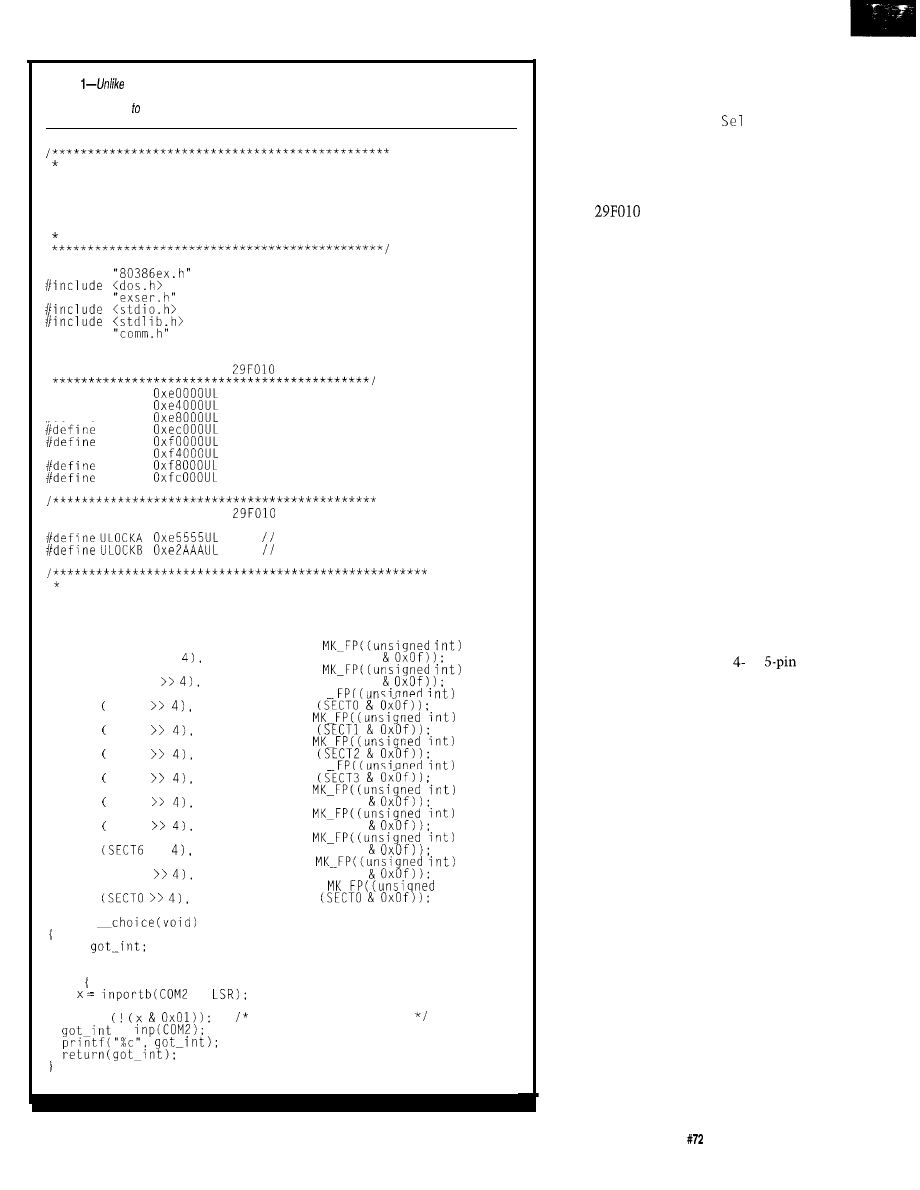
Listing
traditional read-only memory, flash can be modified at any time from a high-level
language like C. Using f/ash, a developer can provide periodic updates to a product’s firmware or design a
system that adapts changing user or environmental requirements.
Flash erase
*
*
Sector erase
*
*
Byte programming
*
*
Chip information:
*
*
Manufacturer code
*
*
Device code
*
Sector protection information
*
#include
#include
i/include
/************************************xx*******
* Sector addresses for a
*
#define SECT0
#define SECT1
#define SECT2
SECT3
SECT4
#define SECT5
SECT6
SECT7
* Unlock addresses for a
*
xx******************************************,
First unlock'"5555"
Second unlock "AAAA"
Pointers to beginning address of each sector,
*
* base ROM address and unlock addresses
*
*************************************x*************,
typedef far unsigned char* FLASHPTR:
volatile FLASHPTR ulocka = (FLASHPTR)
(ULOCKA >>
(unsigned char) (ULOCKA
volatile FLASHPTR ulockb = (FLASHPTR)
(ULOCKB
(unsigned char) (ULOCKB
volatile FLASHPTR sect0 = (FLASHPTR) MK
volatile
volatile
volatile
volatile
volatile
volatile
SECT0
(unsigned char)
FLASHPTR sect1 = (FLASHPTR)
SECT1
(unsigned char)
FLASHPTR sect2 = (FLASHPTR)
SECT2
(unsigned char)
FLASHPTR sect3 = (FLASHPTR) MK
SECT3
(unsigned char)
FLASHPTR sect4 = (FLASHPTR)
SECT4
(unsigned char) (SECT4
FLASHPTR sect5 = (FLASHPTR)
SECT5
(unsigned char) (SECT5
FLASHPTR sect6 = (FLASHPTR)
>>
(unsigned char) (SECT6
volatile FLASHPTR sect7 = (FLASHPTR)
(SECT7
(unsigned char) (SECT7
volatile FLASHPTR rombase = (FLASHPTR)
int
(unsigned char)
int Get
int
int x;
do
+
while
Wait until data comes
=
(continued)
Programming involves issuing the
unlock sequence to the device and
then issuing the command. The first
command is typically
Auto
ect,
so that the proper device type and
manufacturer is identified.
The code in Listing 1 is written in
C. It runs on a ‘386EX target board
with a
flash memory chip,
from which it also boots. The program
demonstrates the common algorithms
for accessing the chip.
Error recovery is eschewed. You can
download programming algorithms
from various manufacturer’s bulletin
boards. This code is just an example.
PROGRAMMING VIA JTAG
Generally, once the algorithms are
in, the flash can be programmed con-
veniently. But, how about program-
ming a flash part that is already on the
board and is totally blank?
This programming is accomplished
over a JTAG port on the CPU, if your
target system has one.
JTAG (Joint Test Access Group)
developed a standard known as IEEE
1149.1. It’s a serial interface to directly
drive the pins of a CPU chip.
The internal circuitry provided on
the chip to support JTAG executes
CPU instructions by feeding them over
the JTAG port. The port is a or
connection with just as many pins for
ground. You see the pins defining the
JTAG interface in Table 3.
This interface is implemented vari-
ously as BDM (Background Debug
Mode) and is also referred to as Bound-
ary Scan.
The lowest-cost interface to the
JTAG port is simply a cable connected
to the parallel port of the PC and a
piece of software feeding the bits to
accomplish the operation.
You can practically run code out of
a host over the JTAG on the target. It
comes in handy when the target mem-
ory system is malfunctioning. But, in
this case, it is used simply to program
the boot code in a blank flash device.
The host-based software feeds and
executes the proper instructions to
program the flash memory in-circuit.
Many debuggers support JTAG for
debugging, and some let you program
flash over the JTAG.
Circuit Cellar INK@
Issue
July 1996
43
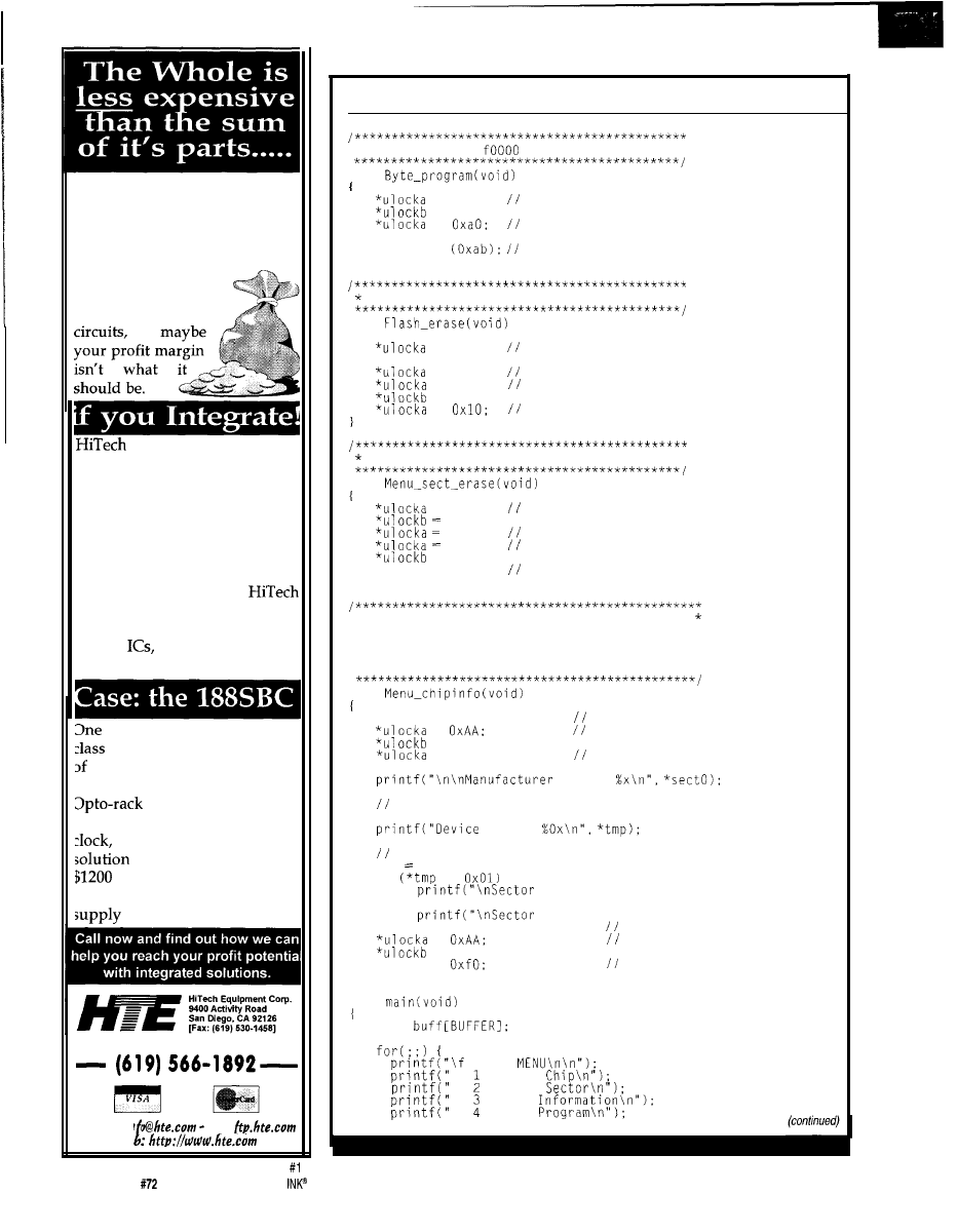
You’re shipping the first systems
out the door, the customer is
happy, and you can breath a sigh
of relief now, right? But can you
really afford to relax now?
If that system was
built using many
different boards and
can combine all those
boards and circuits onto a single
board, saving you big money.
Reduce your unit cost with less
inventory and fewer vendors,
faster assembly time, fewer ca-
bles, and even smaller package
size. Built to your specifications,
an integrated board from
can include analog, digital,
FPGA and even custom mixed
signal
all for less money
than your current solution.
customer needed an x86
processor with 16 channels
12 bit A/D and 8 channels of
12 bit D/A, LCD, Keypad and
interface, two serial
ports, a printer port, real-time
and more. A multi-board
would cost around
each. The 188SBC costs
only $749, and includes a power
and a custom FPGA!
S i n c e 1 9 8 3
VI A
E-mail: in
Ftp:
We
4 4
Issue
July 1996
Circuit Cellar
Listing
l-continued
* Writes Oxab to
(sector 4 base add) *
void
= Oxaa:
unlock sequence
= 0x55;
=
Byte write command
*sect4
=
Write ab to address pointed to by sect4
Chip erase function
*
void
= Oxaa;
Unlock sequence
*ulockb = 0x55:
= 0x80;
Erase command
= Oxaa;
Unlock sequence
= 0x55:
=
Erase chip
Erase sector 4
*
void
= Oxaa;
Unlock sequence
0x55;
0x80;
Erase
Oxaa;
Unlock sequence
= 0x55:
*sect4
= 0x30;
Erase sector 4
* Get chip information
* Displays:
*
* Manufacturer code
*
* Device Code
*
* Sector protection information for sector 3 *
void
volatile FLASHPTR tmp;
Temporary pointer
=
unlock sequence
= 0x55;
= 0x90:
enter autoselect
code =
Device code is located at offset 1 from beginning of ROM
tmp = sect0 + 1:
code =
point to sector-protection offset in sector 3
tmp sect3 + 2:
if
==
3 Protected"):
else
3 Not Protected");
Put flash back in read mode
=
Unlock sequence
= 0x55;
*ulocka =
Read/reset
void
char
int choice:
FLASH
Erase
Erase
Chip
Byte
Listing 1-continued
Enter selection:"):
choice =
case '1':
Flash Erase Comp
case
Erase
break.
case
break:
case '4':
break;
default:
ERROR! WATCH YOUR FINGERS WHEN YOU TYPE
break:
ENTER to continue"):
You can also acquire specific
ware for JTAG operations.
Code development is the easiest
part of using flash.
You
can pretty
much ignore that you’re using a flash
HARDWARE HANDSHAKE
Most of the newer flash devices
allow the target hardware to manage
the flash properly during system reset
or other recovery.
Instead of using the Read Reset
command, a Reset pin on the device
allows return-to-read mode when sys-
tem reset is applied.
Also, instead of polling for a device
to get done, a Busy/Ready pin inter-
rupts the target CPU if necessary to
indicate the device status.
DEBUGGING
In firmware development with flash
memory, you have three separate
tasks:
l
code development
l
flash programming algorithms and
error recovery
l
data storage algorithms
Pin
T C K
Clock for data transfer
T M S
Selects mode to control
which operation
TDI
Serial Data in
T D O
Serial Data out
T R S T
Reset (Optional)
Table 3-A
microprocessor’s JTAG interface can now
be used to program blank
devices after
are
soldered into your target.
device. It’s only a place to store the
finished and debugged software. Code
in the flash ROM is no more peculiar
than code anywhere else. Whatever
techniques you use to develop your
firmware work here just as well.
The software routines that erase
and program flash in-circuit are quite
critical and device-specific. The
generation devices require controlling
the 12-V
programming voltage
and software commands externally.
Voltage level and timing of opera-
tions (e.g., how many times to pulse
the
are externally controlled and
very sensitive to spikes or partial
counts and restarts. This complexity
must be maintained and controlled by
the designer.
Fortunately, for most newer flash
devices, the programming algorithm as
well as programming voltages are in-
ternally controlled. The external soft-
ware simply issues the appropriate
commands and then monitors the
status for completeness.
Keep in mind that flash becomes
busy soon after a command is issued.
Your programming algorithms need to
run from some other memory device
than flash.
Typically, you copy the algorithms
out of flash to some other memory and
Multitasking for:
Borland C/C+ Microsoft UC++, or Borland Pascal
supports:
3.0 or
higher, Embedded
stems without DOS,
Paradigm Took (info available),
o Debugger.
and cooperative
scheduling
Shared
to 64
Code/
runlimited number of
in
tasks,
per
task needed
emel tasks
rate
communication
from
License: $550
complete Source Code: add $5
no run-time royalties
resolution
real-time
through
driven
for
ke board,
up to
ports, I
services, floppy
disks, hard dii
etc.
Development System for:
B o r l a n d U C +
C / C + + , W a t c o m C / C + +
et-32
Intel 1486
(2). as little as
rpro
ram download
at
15200 baud
paging
remapping
standard
communications
PCs and controller
library
boards
level
memory
supports the
model with
U C + + r u n - t i m e
physical logical
systems
for Win
addresses
etc.)
PE-files
License:
complete Source Code: add
no run-time royalties
Circuit
Cellar
INK@
Issue
July 1996
45
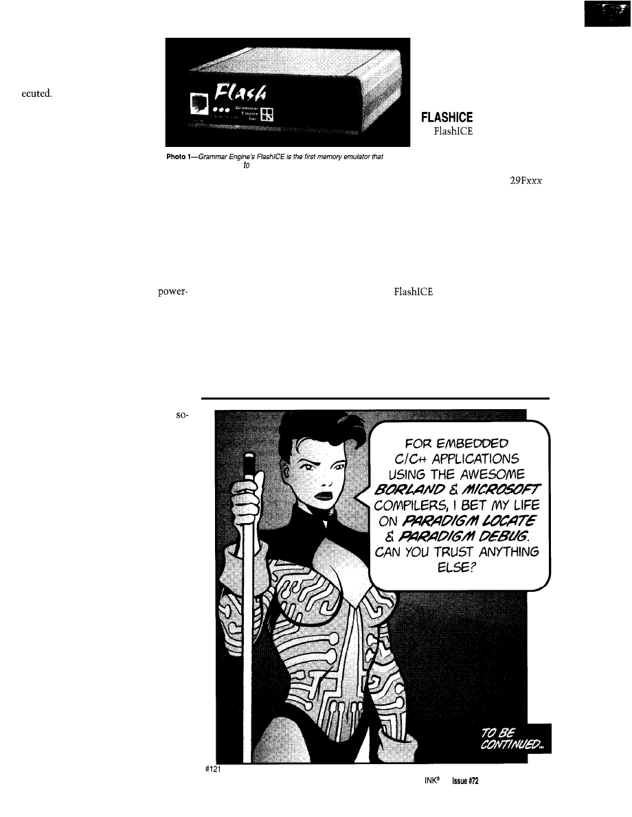
execute them from there.
Failures here are caused by an
interrupt routine requesting
code from the flash to be ex-
Appropriate handling
of such conditions has to be
part of the algorithms.
All write operations, like
sector- or chip-erase, take
time. Even simple operations
such as writing a byte make
the device appear busy. It is
recognizes and responds flash commands.
imperative that, for proper operation,
the algorithms verify the operation.
Your system should include some
sort of checksum for verifying that the
operation completed successfully. On
the surface it seems simple, but imag-
ine a power failure during a flash pro-
gramming cycle. Unless your software
can verify the sanity of flash on
up, the incomplete programming cycle
may not be detected.
Unfortunately, no tools are avail-
able in the marketplace to tell you
how and what you’re doing to the
flash. You pretty much have to try and
see.
It can be very difficult to verify your
algorithms and test error conditions
and handling of device failures. The
called boundary conditions are impos-
sible to test since flash devices most
likely won’t experience any failures
until they’ve been out in the field and
used for a while.
That’s when you find out that,
because of faulty algorithms, the
device’s lifetime is severely reduced or
specific locations are getting burned
out. Before we dive into what kind of
help is available for testing the algo-
rithms, let’s consider the third devel-
opment issue related to flash.
Believe it or not, data storage is the
main advantage and feature of the
flash. Flash is intended for storing data
more than code. As mentioned earlier,
it provides high-density, low-power,
nonvolatile data storage on-the-fly.
Generally, data storage is organized
as a file system, but it doesn’t have to
be that elaborate. Very often, the im-
plementation specifically addresses the
product’s need.
The main consideration here is that
the flash device has a useful life. Its
usefulness is measured in the number
of erase/write cycles that can be done
on a location. The numbers for older
devices are on the order of 10,000 and
for the newer devices are more like
100,000. In real life, you may get a
million useful cycles out of the part.
However, the software that deals
with the flash must ensure that proper
programming is achieved. Since fre-
quently used locations may wear out,
smart software includes “wear-level-
ing” algorithms.
It all boils down to this. How do
you know that you’re doing all the
right things in the software-every-
thing from proper commands to the
flash, proper handling of the
error conditions, and proper
wear-leveling?
The answer: you can’t-at
least not until now.
(see Photo 1) is a
ROM emulator with special
circuitry to emulate flash
functionality. As a new prod-
uct, it only supports
parts.
Since the software access to the
embedded algorithms follows a state
machine, it’s possible to emulate and
verify proper access to the flash. This
emulator plugs in where the flash
normally goes and then behaves like
flash memory.
is unique because it not
only emulates the ROM, it also moni-
tors and reports the flash functions. It
effectively provides a back end to the
flash device.
The interface to the host system
lets the user monitor all flash access as
well as setup error conditions. The
Circuit Cellar
July1996
47
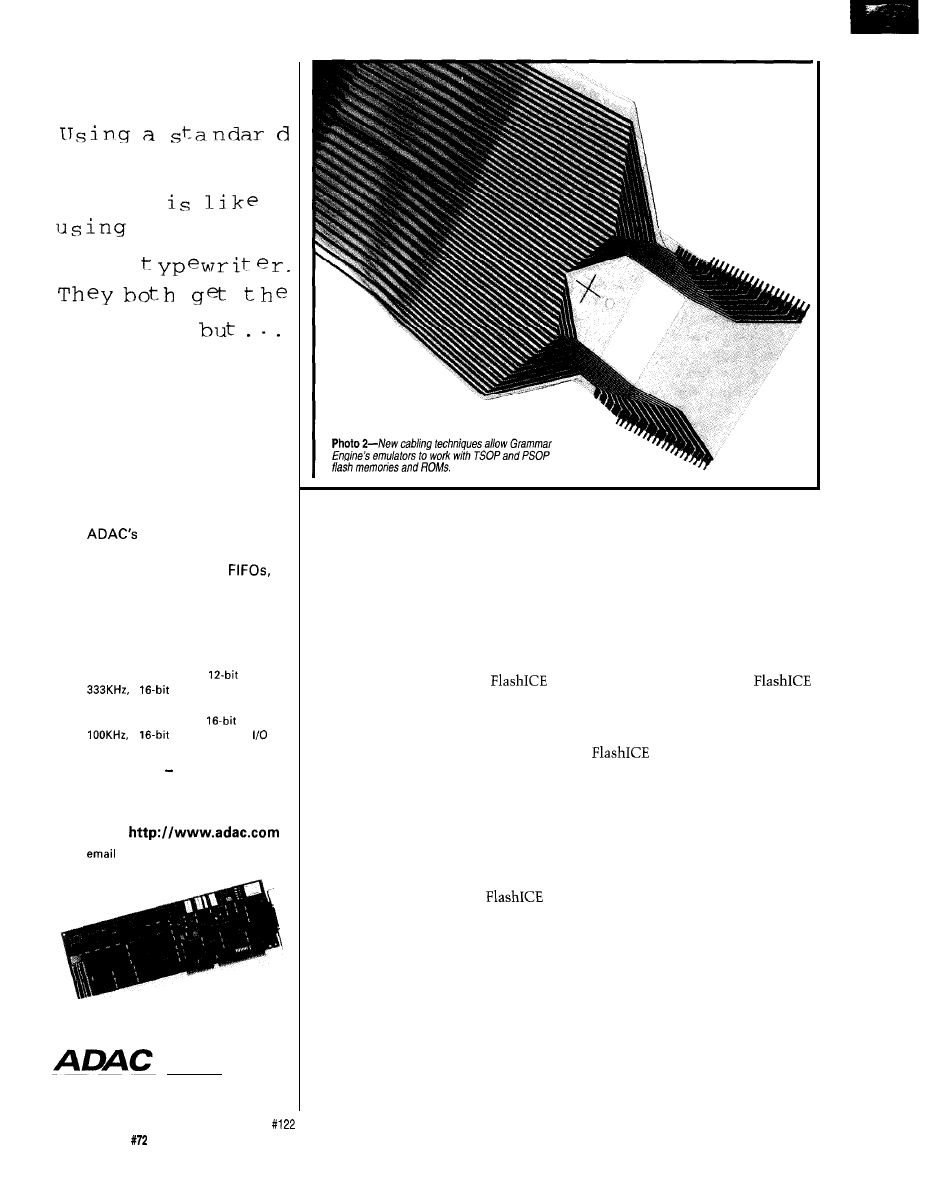
Running under
Windows?
&to acquisition
board
an old
job done,
there is a
better way.
Standard data acquisition
boards can unknowingly
sabotage your data. Ensure
the integrity of your results.
Windows Optimized
5800 Series gives you the
resources you need:
Channel Gain RAM, Dual
DMA, aggressive prices,
and some of the best noise
performance in the industry!
5801MF:
16 channel
A/D,
2
D/A, 40 digital I/O
5803HR:
16 channel
A/D,
2
D/A, 40 digital
learn more
voice 800-648-6589
fax
617-938-6553
web
info@adac.com
American Data Acquisition Corporation
70 Tower Office Park, Woburn, MA 01801 USA
user then accomplishes three different
nately, they don’t necessarily go away
things:
if there is a socket.
l
they can verify programming algo-
rithms on the target system. By
monitoring the host interface, er-
rors in the target system software
relating to erasing or programming
the flash can be discovered
l
they can log flash activity.
logs all flash access (other than
reads) on the host system, so the
user can monitor the extent of flash
activity and its use by the target
system
Even though you can buy flash
devices in the standard DIP format, it’s
generally available only in fine-pitch
surface-mount parts. It is intended to
be soldered on.
Sockets are available for just about
any footprint. That makes it a little bit
easier to attach a device like
to the target system. Very often, how-
ever, the socket is delicate and attach-
ment to it requires custom cabling.
l
they can force error conditions. The
user tests the target software’s error
handling by specifying certain fail-
ures to be simulated
currently supports cables
for connection to TSOP and PSOP
parts. Photo 2 shows a TSOP cable.
SYSTEMDEBUGHEADER
Finally, with the flash interface
extended by one command,
implements a virtual serial channel
between the host and the target sys-
tem.
This proposal is brand new, but the
concept is fairly simple. Essentially, a
fine-pitch header occupies a small
amount of space on the target board.
This channel enables the host-based
debugger to debug target software via
ROM monitors. It may be used for
other purposes as well.
The system debug header directly
connects to external tools, such as
ROM emulators, for debugging and
developing software. This header is not
specific to a given system or device. It
emulates simple ROMs or flash mem-
ory or monitors target activity without
emulating anything.
CONNECTION TO TARGET SY STEM
Real problems arise if the flash part
is soldered on to the board. Unfortu-
The driving need for defining such a
connector is to provide a universal
means of connecting to an arbitrary
48
Issue
July 1996
Circuit Cellar
INK@
target for various development pur-
poses. Such a header can be built into
any target regardless of what else is
It can be used during develop-
ment or even for servicing the embed-
ded system in production.
Those familiar with JTAG realize
that it is limited in its capabilities to
access the processor or other
devices supporting the JTAG interface.
However, this header is much more
useful and allows simpler and general-
ized access to the target system.
Short of something like the system
debug header, there’s no method of
developing for systems that have fully
soldered-on components. As time goes
by, some generalized and universal
means must be established to provide
effective but simple access to the tar-
get system.
Arvind
founded Grammar En-
gine, a company that has pioneered
the art of ROM emulation and debug-
ging in the ROM socket. He previously
worked for CompuServe and
Bell Labs. You may reach Arvind at
Advanced Micro Devices, Flash
Memory Products Data Book/
Handbook,
1996.
Advanced Micro Devices, Introduc-
tion to
and Five-Volt
Programming with MACH 3 and
4 Devices, Application Note
1996.
Corp.,
Nonvolatile
Memory Data Book, 1995-1996.
Intel Corp., Flash Memory: Volume
I, 1995.
System Debug Header
Grammar Engine, Inc.
921
Dr., Ste. 122
Westerville, OH 4308 1
(614) 899-7878
Fax: (614) 899-7888
410
Very Useful
411 Moderately Useful
412 Not Useful
be famous?
re you or your company using
technology in an
interesting or unusual way?
Tell us
about it.
DESIGN CONTEST
You are invited to submit unique
projects or applications to our design contest. sure to
functional block diagrams with descriptions of the hardware, software. and peripherals used. Contest
entries will be judged for technical merit, applicability. and originality. The judges: Circuit Cellar INK’s
Steve
Rick
and Embedded PC’s
Editor Janice
We’ll
highlight winning applications in Embedded PC, plus designers will be
up for a future
Quarter. And there’s more! Winners will
l
1st prize
__
Development Kit
. 2nd
Development Kit
. 3rd prize
Development Kit
All entries must be received no later than August IS,
Winners will be announced at September’s Embedded’
Systems Conference and the winning project
will appear in December’s issue
Cellar INK.
Contact us today for your entry form and then
mail your contest entry to:
Janice
Quarter Contest
Circuit Cellar INK 4 Park Street Vernon. CT 06066
Tel: (860) 875-2199 Fax:
w w w :
E-mail:
Cosponsored by
Computers. Inc.. the originator of
and Circuit Cellar INK. home of Embedded PC.
Be a hero put Team
work on
next
embedded x86 design and reap the rewards you deserve.
Paradigm has the ability to deliver all the embedded
system pieces from Intel to AMD, C/C++ or assembly
language, and all the Borland/Microsoft development tools.
Plus
Paradigm DEBUG
for your favorite in-circuit emulator
and real-time operating system.
So forget about making excuses and instead enlist
Team Paradigm for your current or next x86 project. We
deliver the finest embedded x86 development tools, backed
by unlimited free technical support. No one is more serious
about your success than Paradigm Systems. Call today
and get the details before you waste any more of your
precious time.
Proven Solutions for Embedded C/C++ Developers
I-800-537-5043
Paradigm Systems
3301 Country Club Road, Suite 2214,
NY 13760
(607) 748-5966 FAX: (607) 748-5968
Internet: 73047.30310
Paradigm Systems. Inc. All
reserved.
Circuit Cellar INK@
Issue
July 1996
49
Bob Meister
Simulator on a
Personal Computer
new, I cut my teeth on a
DEC PDP-8 minicomputer. It ran at
only 1.2 per cycle with 8 192
words of magnetic core memory.
PDP-11 MINICOMPUTER FAMILY
The PDP-11 was a 16-bit extension
to the
PDP-8 computers. Those
16 bits gave the PDP-11 an addressing
range of 65,536 bytes and increased the
number of registers from the PDP-8’s
single accumulator to eight
purpose registers.
It used a Teletype ASR-33 as the
keyboard, printer, and paper-tape read-
er and punch. It had a front panel with
switches and lots of lights that burned
out. If you were lucky, it had some 8”
floppy disks that held 256 KB of data
apiece.
There are over 70 instructions,
most of which deal equally well with
bytes or
words. All instruc-
tions access data in memory or regis-
ters. It makes no difference to the
CPU.
In 1978, the
version of
LSI-11 single-board minicom-
puter cost about $1300 and consisted
of a card cage, CPU, power supply, and
enclosure. For this price, you didn’t
even get a serial interface, but the CPU
board came with 8 192
bytes of
dynamic memory.
The effect of most data manipula-
tions is stored in a Processor Status
Word (PSW) that has flag bits for carry,
overflow, negative, and zero. This PSW
exists at the highest address in the
machine, 177776 octal.
I bought a serial interface for $100
and connected it to a Teletype ASR-33.
Another $100 purchased an additional
8 KB of memory. Two years later, I
bought a dual-drive 8” floppy-disk
subsystem with a
total capac-
ity for the (now) unbelievable price of
$1900.
The I/O devices use
mapped I/O, rather than separate I/O
instructions or an I/O bus. The PDP-11
reserved address space for the device
registers, which were handled like any
other memory address by reading or
writing their contents.
The PDP- 1 l’s memory layout re-
serves locations in low memory for
interrupt and trap vectors (O-477 oc-
tal). Available main memory usually
goes up to 56 KB.
Although those good old days are
The last 8192 bytes are the I/O
gone, I wasn’t altogether ready to give
page, which hosts specific hardware
them up. I loved writing code on my
and the CPU’s internal registers. The
LSI- 11, primarily in assembler lan-
PDP-1 l’s interconnecting bus provided
guage. So, I decided to write a program
16 bits for data, several control lines, 4
to run PDP- 11 binary code directly on
a PC.
I was determined that the program
look and act like an LSI-11 system.
And, I succeeded. My LSI-11 program
runs on an 80x86 and executes PDP-11
instructions.
Granted, since it’s interpreting
binary code, it runs at a slower rate,
but there’s not much that can be done
about that. The simulated program’s
speed depends on the number of in-
structions required to execute it on a
target machine.
While the program and the instruc-
tions executed are particular to the
LSI- 11, the principles in this article are
common to many simulators and can
be transferred to other target proces-
sors.
5 0
Issue
July 1996
Circuit Cellar INK@
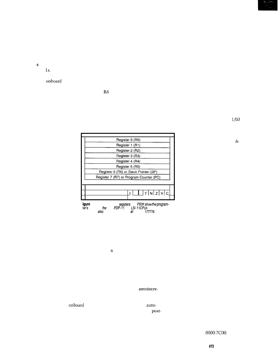
interrupt request lines, and 18 bits for
addressing up to 256 KB of memory.
Memory-management hardware
extended a program’s memory-access
range to several banks of 64 KB each.
With more than 64 KB of memory, the
I/O page moves to the highest 8-KB
area from 248 to 256 KB.
The LSI- 11 are single-board ver-
sions of the PDP-1 Besides not hav-
ing the PDP- 1 l’s front panel, the
LSI-11 had 8 KB of
memory
and a microcode routine to examine
and change registers and memory loca-
tions. When the CPU executes a Ha 1 t
instruction, it enters this microcode,
commonly referred to as the Octal
Debugging Technique (ODT) control
routine.
Four more addressing lines in the
interconnection bus enable pe-
ripherals and some LSI- 11 models
to access up to 4 MB of memory.
The newer interconnecting bus
multiplexes the address and data
lines to save space. Unfortunately,
this feature slows the bus up
somewhat.
The original LSI- 11 CPU only
recognized one interrupt-request
line. Later models returned to
four. The PSW became an internal
register, and new instructions
were developed to access it. (Some
later LSI- 11 models also accessed
l-General-purpose
and
mode/ of
basic
and
On some
mode/s,
instructions. Although data is nor-
mally transferred to and from main
memory, a memory-mapped I/O device
can be the target of such a transfer,
assuming its address space is large
enough.
PDP-11 ARCHITECTURE
As Figure 1 shows, the PDP- 11 has
eight general-purpose registers. R7 is
the Program Counter (PC), which is
often used by instructions, but not
usually modified directly.
The Stack Pointer (SP) may be
used as a general register but subrou-
tines and interrupts also use it and the
memory it points to. The other regis-
ters can be used with any instruction
and addressing mode. Registers aren’t
tied to certain instructions.
Processor Status Word (PSW)
the PSW located at 177776 octal.)
the
PSW is
accessed as a word address
The PSW holds the condition code
The instruction set is fairly robust.
Almost all data-handling instructions
deal with byte data as easily as word
data. Registers and memory (including
memory-mapped hardware) are treated
equally. Data can be moved between
any source and destination.
When used with the PC, a few of
the addressing modes become the
more familiar immediate, absolute,
and PC-relative modes. Through this
technique, you can write code that
runs independent of the address it is
loaded into since all data references are
relative to the current value of the
program counter.
PROGRAM IMPLEMENTATION
I
wanted to simulate the LSI-1
and have it run programs under the
RT-11 OS. It had to execute each
LSI-11 instruction like the real
thing, which meant having a
KB memory space available. The
C Small model (64 KB for code,
64 KB for data) seemed perfect
for this solution.
The LSI- 11 simulator begins
with command-line argument
processing and some once-only
initialization code. The com-
mand line specifies which DOS
files and/or floppy drives are
seen as logical units by the
RT-11 OS.
I wrote a device driver called
PF (Personal-computer Floppy)
PDP-1 l’s had a unique inter-
rupt system. Depending on the proces-
sor, one or four interrupt-request lines
were available. An interrupt-request
signal passes through each interface
board in the backplane to the CPU.
Boards physically closer to the CPU
have a higher priority.
When the CPU acknowledges an
interrupt, the board requesting it pre-
vents the acknowledgement signal
from reaching any lower board trying
to interrupt. When the higher-priority
board finishes, the lower-priority
board’s interrupt request is processed.
Direct Memory Access (DMA) is
also provided. Unlike the PC’s
DMA, each interface board has its own
DMA hardware to transfer data be-
tween the peripheral and memory.
The CPU arbitrates DMA requests
and relinquishes bus control between
flags and an interrupt-enable bit. The
larger PDP- 11 and LSI- 11 models have
additional bits within the PSW for
multiuser environments.
PDP- 11 operate with the octal
numbering system. One three-bit digit
represents a register, while another
digit defines the addressing mode. The
eight addressing modes combine with
any of the eight registers. Some of the
useful modes are: register direct, regis-
ter indirect, indirect with
ment, indirect with autodecrement,
indexed, and indexed indirect.
For the autoincrement and
decrement modes, the register is
incremented or predecremented by one
for byte instructions or by two for
word instructions, which are always
aligned on even addresses.
that handles eight logical units or
devices. Any device that can contain a
directory and be randomly accessed
can have a bootstrap put on it.
If floppy disks are used, the simula-
tor allocates a one-track buffer in
memory so that it won’t span the PC’s
64-KB address boundary. This buffer is
needed to read more than one sector
per disk request.
The simulator also clears the gen-
eral-purpose registers and reads the
bootstrap block (block 0) from the first
device or file specified on the com-
mand line into location 0 of simulated
memory. Execution begins at location
0 where the simulator finds the first
instruction.
This procedure is comparable to the
PC’s bootstrap that loads the first disk
sector into address
On
Circuit Cellar INK@
Issue July 1996
51
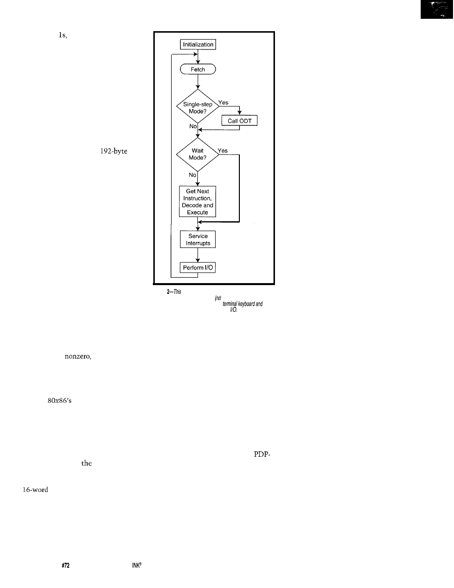
some LSI-1
a
bootstrap ROM
prompts for a device’s standard DEC
two-letter name and logical-unit num-
ber. My simulator provides this selec-
tion functionality by always booting
the device or file associated with PFO.
For the instruction decoder, I ini-
tially used an array of 65,536 byte
values indexed directly by the instruc-
tion word. A value from
1 to
17 selects
the major instruction group. Since the
same functionality was available by
using only 13 of the
16
instruction
word bits, I now use an 8
array. I generate an index into the
array by shifting the instruction word
right by 3 bits.
The various decoded cases perform
requested operations by turning off
specific PSW bits, obtaining source
and/or destination addresses, fetching
source and/or destination data, per-
forming operations, setting specific
PSW bits, and storing the results.
While branch instructions don’t
have operands, they do force a change
in the program counter if a specific
combination of PSW bits exists. Obvi-
ously, certain instructions are simpler
to implement.
Most instructions were easy to
code. Difficulty lay in managing the
appropriate PSW bits based on the
result of executing the instruction.
Performing a mathematical operation
in C or any high-level language pro-
duces a zero,
positive, or
negative result. Determining if the
result should set the carry or overflow
bits requires more work since C
doesn’t know about these outcomes
and the
flags can’t be obtained
on an instruction-by-instruction basis.
I test the input data for conditions
that cause a carry or overflow and then
set the appropriate bits. These addi-
tional statements require longer execu-
tion time.
I also enhanced
branch-instruc-
tion logic. I used the four condition
code bits of the PSW as an index into a
array. I convert the branch
instruction into one of
16
bits and test
this bit in the array’s word. If set, a
branch occurs, and the PC adjusts
accordingly. This streamlines the logic
considerably, making all branch in-
structions operate at the same speed.
52
Issue
July
1996
Circuit Cellar
Service
Interrupts
Perform
Figure
flowchart
depicts the main simulator
process. Additional routines shown) handle
addressingmodedecoding,
screen emulation, and file and disk
Like all computers, instructions
execute sequentially. At the end of
each instruction, several tests handle
single-step mode, deal with pending
interrupts, check for operator console
intervention, process outstanding I/O
operations, and maintain housekeep-
ing duties normally performed by a
CPU. Figure 2 shows the simulator’s
process.
DEALING WITH “HARDWARE”
The I/O device-register code was
the most difficult to get working. Re-
member the address space of the
1 l’s I/O page is typically the upper
8 KB.
In the simulator, the main memory
goes up to 60 KB, leaving only 4 KB for
I/O (see Table 1). This arrangement
gives programs more breathing room
and is safe as long as I/O devices are
limited to the upper 4 KB.
A subroutine in the simulator de-
codes the source or destination ad-
dressing mode and register bits and
sets a pointer to the operand’s address.
When the address is determined, it is
compared to the highest memory ad-
dress to check for known I/O address-
es.
If the operand accesses a legal de-
vice or memory address, everything
proceeds normally. If the program
attempts to access an address where no
device or memory is present, the simu-
lator performs a
TRAP
indicating non-
existent memory.
A
TRAP
or interrupt pushes the PSW
and PC onto the stack, and a new PC
and PSW are obtained from predeter-
mined vector addresses. All interrupt
vectors contain these two words to be
put into the PC and PSW. An
RT I
instruction pulls the stacked PC and
PSW back where they belong.
Assuming a program wants to ac-
cess a hardware-device register and has
the correct address, the simulator
points to the pseudoregisters of the
hardware devices. These bytes are
modified by the running program.
Periodically, these pseudoregisters
are tested for certain conditions, such
as data output to the screen. If re-
quired, an I/O operation using the host
PC’s real hardware (e.g., keyboard,
screen, line printer, and disk and file
I/O) is performed.
For the keyboard, a PC BIOS func-
tion checks for keystrokes. If so, a bit
is set in the pseudoregister that a run-
ning LSI-11 program can test.
In addition, most hardware devices
interrupt when a significant event
occurs (e.g., keyboard input or disk
operation completion). If a device reg-
ister has interrupts enabled, the simu-
lator acknowledges the interrupt by
saving the present PSW and PC and
picking up new ones at predetermined
addresses.
In a real system, pending interrupts
are recognized and serviced if the
CPU’s priority allows at the comple-
tion of each instruction. The simulator
checks specific flags set when an I/O
operation generates an interrupt.
The appropriate interrupt vector is
accessed and instructions continue at
the new location specified. If no de-
vices request interrupts, the necessary
I/O operations get done.
By processing interrupts and
I/O requests in this order, I intro-
duce a few instructions of inter-
rupt latency. With this delay, the
simulator more closely repre-
sents a real LSI-11, since few
devices can immediately
Octal
Address Range Typical LSI-11 System Usage
170000-177777
160000-l 67776
I/O page (device registers)
RT-11 monitor and device drivers
001000-l 57776
000500-000777
Runnable program space
000000-000477
Program stack space
Interrupt vectors
interrupt, and complete
tasks.
Table 1
60
KB of simulated RAM decodes
addresses of
167776. Standard device addresses are decoded separate/y
and do not actually exist in simulated memory space.
Since the simulator can’t deal
with parallel events, I test flags every
100 instructions. If an I/O event starts
that interrupts on completion,
I
test
every three instructions. This action
shortens interrupt latency so the inter-
rupt occurs closer to the generating
event.
form mask and bit-set operations to
maintain specific bits in the same
condition the real hardware would.
Although this code only occurs
every 100 instructions, it’s extra code
which slows the simulator down.
an interrupt through the nor-
mal vector.
The RT-11 OS supports an LTC.
Using c t i me
I read the host sys-
tem’s date and time. I tracked the
number of seconds between successive
calls. When there was a one-second
difference, I multiplied the number by
60 (60 ticks per second) and forced
interrupts through the proper vector
until the tick counter reached zero.
Real LSI-11 computer sys-
tems contain a 60-Hz signal
from the incoming power line,
or LTC (Line Time Clock).
Depending on the system, the
hardware generates a real inter-
rupt, or an LTC signal is fed
into a separate event line on
the CPU board, which causes
Real LSI-11 hardware interrupts
immediately on event completion. For
a time-critical application, 80x86 in-
terrupt service routines could set bits
in a control word, which the simulator
could check and respond to.
Some device registers contain
only bits. Writing zeros to them re-
sults in a certain bit combination in
the real hardware. The simulator had
to test for these conditions and
DISK AND DEVICE INTERFACING
I used the PC’s BIOS routines for
the LSI-11 video, keyboard, and print-
er. I added support for a Hazeltine
model 1510 VDT. This model trans-
lates the escape sequences into calls to
the video BIOS to clear the screen,
position the cursor, and so on. It also
translates certain
into the
multiple-character sequence a real
terminal’s keyboard sends.
The clock kept perfect time since it
received 60 counts each second, even
though all 60 occurred in a tight loop
at one time each second. It was perfect
for system clock timekeeping.
Of course, one program wanted to
delay a message
for a number
of seconds. The program counted the
chase”. Brand
drives.
new, dual speed,
Complete with drivers. At B.G.
Micro, CD means cost dropper.
don’t even believe this
sive SCSI controller card
power their alarms with
(quit glancing at the price and these plug-in transformers.
read
I
this ad) on the market, Manufactured by Basler
It’s great for cd roms, hard
UL approved. Can also
drives, etc.
What’s the be used for
cell charger,
I
catch? The only catch that etc. Actually, we don’t care
we can find is that you can’t what you use it for, as long
boot from it. 8 bit scsi card as you buy it. Plug-in
with drivers $19.95 former
2
screw terminal output. Note:
output voltage is AC at
Easy to
use-Out perforn
LM-317 and is ratt
at a full 2
C251
EMBEDDED CONTROLLERS
RIGEL Corporation introduces its newest board, the
designed for Intel’s
chip. RIGEL builds and supports 8
16 bit development tools for embedded controller systems.
feature hardware, software, books, and kits, for educational
industrial markets.
THE RIGEL DIFFERENCE
All of our boards come
with:
. 32KEPROM
l
32K RAM or EEPROM
l
Machine screw sockets
l
Power on LED
l
All system signals
on headers
l
available on
terminal blocks
l
Sample programs
l
Circuit diagrams
l
Assembly language
IDS software READS
l
BBS Tech support
Our entire line of
8051
boards are
programmable in
Assembly, BASIC,
and Forth. We also offer a low cost Fuzzy
Logic Software code generator and a chip simulator for the 8051
family.
Complete systems start at $85
CALL TODAY FOR MORE INFORMATION
RIGEL Corporation,
PO BOX 90040, GAINESVILLE, FL 32607
Telephone (352) 373-4629 BBS (352) 377-4435
Circuit Cellar
Issue
July 1996
53
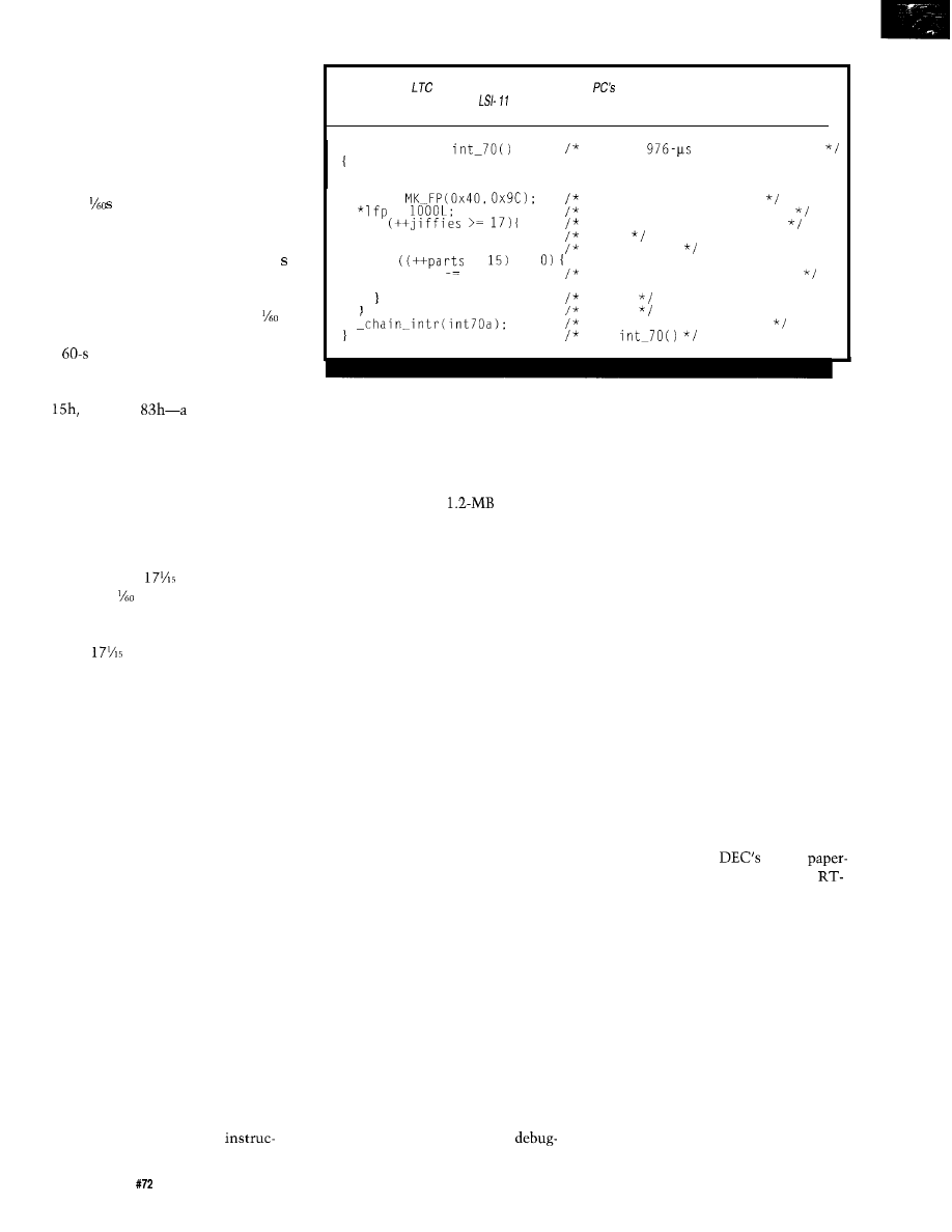
number of instructions the CPU could
execute in a loop between two succes-
sive LTC interrupts after skipping one
for synchronization. It then multiplied
this count by 60 to calibrate a delay
loop of 1 s.
On a real LSI-11 system, where the
same
exists between LTC inter-
rupts, this worked fine. On the simula-
tor, the program measured the time
between the last pseudointerrupt 1
ago and the one presently happening. It
assumed this large number of counts
equaled the amount of time for
s,
and multiplied it by 60. The result was
a
delay for every second required
by the program. Oops!
I first tried the ROM BIOS interrupt
function
function that
sets up a timer and interrupt service
routine that works in conjunction
with the CMOS RTC available on PC/
AT clones. The clock accepts a value
in microseconds, but interrupts at
1024 times per second, rounding the
given value to within one tick. Con-
verting these 1024 ticks into 60 ticks
yields exactly
of the PC’s inter-
rupts per
s.
My interrupt service routine resets
the timer and increments a counter
every
ticks (see Listing 1). In the
simulator’s main code, I generate a
pseudointerrupt for the LTC whenever
this counter is greater than zero.
This worked fine until I ran the
simulator in the DOS box under Win-
dows. The clock then froze, probably
because of Windows’ time-slicing and
feeble attempt at multitasking. How-
ever, the benefit of real LTC interrupts
far outweighs the need for running in
Windows. Real interrupts also allow
the simulator to run faster. So, I didn’t
worry about this problem.
I simulated a printer interface by
using the PC’s BIOS printer code to
output a character and obtain the sta-
tus. Real LSI-11 systems only have an
error bit to indicate the condition of
the printer. I manipulated the various
PC bits to create the desired effect.
Although the current implementa-
tion prints, it’s very slow. The printer
driver checks to see if the printer will
accept data. If it won’t, it sets the in-
terrupt enable bit and returns to the
calling program. After 100
54
Issue
July 1996
Circuit Cellar INK@
Listing l--The
interrupt service
routine uses the
1024-p
timer to generate the 60 ticks per
second that are provided by a real power supply.
void interrupt
long far * lfp:
lfp =
=
if
jiffies = 0;
ltccnt += 1;
if
%
==
jiffies 1;
parts = 0;
process
timer interrupts
where count interval is
reset counter for more time
done enough for 16.667 ms?
reset
count a tick
add one jiffy every 15 ticks
end if
end if
do the original code now
end
tions, the interrupt condition is de-
tected and serviced. A lot of real time
passes between data transmissions,
The disk interface was originally
implemented with
floppies. I
performed single-sector reads from and
leaving a lot of room for improvement.
writes to the floppy. This was slow,
but I coded it without problems.
I preset some of the disk’s charac-
teristics, so only a drive letter had to
be specified on the command line.
Eventually, I expanded the disk inter-
face to allow any DOS or UNIX file
containing an image of an RT- 11 sys-
tem disk to be read or written.
I also enlarged the disk buffer to
deal with an entire track at a time,
rather than a single sector. Presently,
the disk interface works with any
floppy disk that has 80 tracks, 2 heads,
and a user-specifiable number of sec-
tors per track.
I/O operations are performed by the
PC’s BIOS and DOS services before the
simulator processes the next instruc-
tion. Real hardware interrupts are
handled with counters and various
condition tests.
PCs and DOS don’t generally use
interrupts. A normal DOS program
waits for I/O to finish before going on.
Other than the line-time interrupts, all
I/O takes place instantaneously as far
as a simulated program is concerned.
VERIFICATION AND TESTING
Some testing with a real LSI-11 was
necessary to learn which bits changed
under certain conditions. For
ging, I wrote and compiled small pro-
grams (fewer than 10 instructions) on
After several runs, I knew I needed
my LSI-11 and then attempted to de-
a better way, so I added an ODT rou-
tine to the simulator. I could then code
bug them on the simulator.
some machine-language instructions
into memory, execute the code, store
the results, and examine the various
registers.
To make a device driver deal with
the floppy disk “hardware,” I invented
some memory locations and register
configurations based on common stan-
dards, picked the functionality I de-
sired, and modified an existing device
driver to put RT-1 l’s parameters into
the simulated device registers.
I integrated this into the existing
LSI-11 program’s floppy-disk routine. I
placed the real calculating burden on
the PC where instructions aren’t simu-
lated.
I copied a set of
LSI-11
tape diagnostic programs onto the
11 floppy disks and wrote a program
loader, so I could run them without a
paper-tape reader. This loader was
modified to read a program from a
known place on the disk.
To get the RT-11 OS disk to work, I
chose another diagnostic-one that
tested traps and other oddities of the
LSI-11 processor. However, it took a
third diagnostic, one that dealt with
interrupts, before it actually booted.
Once I had a functional operating
system, I tried all the programs I could
find. One program scanned the entire
64-KB address space, printing the exis-
tent and nonexistent addresses. With
this memory map of main memory, I
could track device registers that re-
sponded when read.
Various programs verified the sys-
tem and processor, and printing was
normal, albeit slow. The LTC kept
perfect time, even during operations
that would have disabled interrupts for
a significant amount of processor time.
In other words, everything that ran
on a real LSI-11 computer ran on my
simulator. I tested the simulator on a
‘386-40, a ‘486-33, and a ‘486-66. Each
ran the program and operating system
identically, except for the respective
speed differences.
Since the simulator initially pro-
cessed instructions by sequencing
through an optimized list of opcode
patterns, instructions found first were
executed fastest.
I spent a lot of time counting in-
structions and optimizing instruction
order. All of this optimization was
unnecessary once I used a table lookup
for instruction decoding.
FUTURE ENHANCEMENTS
I plan to implement a serial port to
allow file transfers via Kermit or its
equivalent. To keep up with the PC’s
speed and not miss characters, I need a
PC interrupt routine for the serial port
and other I/O devices.
The ODT routine should be able to
modify the hardware’s simulated regis-
ters, but small programs in main mem-
ory can do the same thing.
The ability to reboot the computer
from within the ODT would be conve-
nient. Right now, the user can exit the
simulator and press F3 or retype the
entire command line to reboot.
A more useful terminal emulation
would be one of
VT- 100 series.
These are similar to ANSI, although
the state machine handling the escape
sequences is more complex than the
Hazeltine 1510.
I’d like to access an MS-DOS file
from within RT- 11 and vice versa. I’ve
already written a DOS program that
reads files from an RT- 11 volume.
I have another RT-11 program that
knows how to deal with a DOS floppy
disk, but there should be an easier way.
When you’re designing the environ-
ment, you have the luxury of being
able to create new, custom operations.
Give it a whirl. It’s an experience
worth having.
I’d like to thank my officemate, Chris
Hilton, for pointing out the timer
routines, helping to sort out the inter-
rupt mechanism, and for the use of his
systems as an additional test of the
simulator’s operation.
Bob Meister is a programmer/analyst
at the National Association for Securi-
ties Dealers. He’s been fixing and
programming computers for over 20
years and has written simulators for a
DEC PDP-8 minicomputer and a Mo-
torola
microprocessor. Bob
may be reached at
413 Very Useful
414 Moderately Useful
415 Not Useful
CIRCUIT CELLAR
. PROJECT FILE, VOL. II
Audio Sampling System
Wiring Your House for the 21st Century
Multiprocessor Architecture using DSP
ANDMUCHMORE!!!
VISA,
or International Postal Money
Order (U.S. funds drawn on U.S. bank only)
Circuit Cellar
Flee
Street
Tel:
875-2 199
Vernon, CT06066
872-2204
‘includes domestic delivery.
Please
add per copy for delivery to Canada
Mexico.
add $8 per
for
to other non-U.S. addresses.
56
Issue July
1996
Circuit Cellar INK@
Firmware Furnace
Ed
From the Bench
80x86 Performance
Touring the CPU Spectrum
Silicon Update
nce upon a time,
when I was the
departmental New
Kid, I worked down the
hall from a guy whose job it was to
determine the performance of
built mainframe
The architecture wizards gave Dan’1
the plan du jour. He wrote yard upon
yard of FORTRAN code, and ideally,
the results determined what we under-
lings would design and build.
His programs read instruction-trace
tapes from existing mainframes, trans-
lated opcodes into their new equi-
valents, recomputed the timings,
simulated superscalar dispatching
(even though that term hadn’t been
coined yet), figured the effect of new
cache-management strategies, and
combined everything into an overall
CPU-performance rating.
And, Dan’1 got it right, too, within a
surprisingly small margin of error.
High-end microcomputers incorpo-
rate many of the same design features
found in those late- 1970s mainframes.
That’s not surprising, as a single IC
now has roughly the same number of
transistors as an entire mainframe
CPU.
With fortunes made or lost on how
one implementation stacks up against
another, performance prediction is a
critical part of the business plan.
58
July
1996
Circuit Cellar INK@
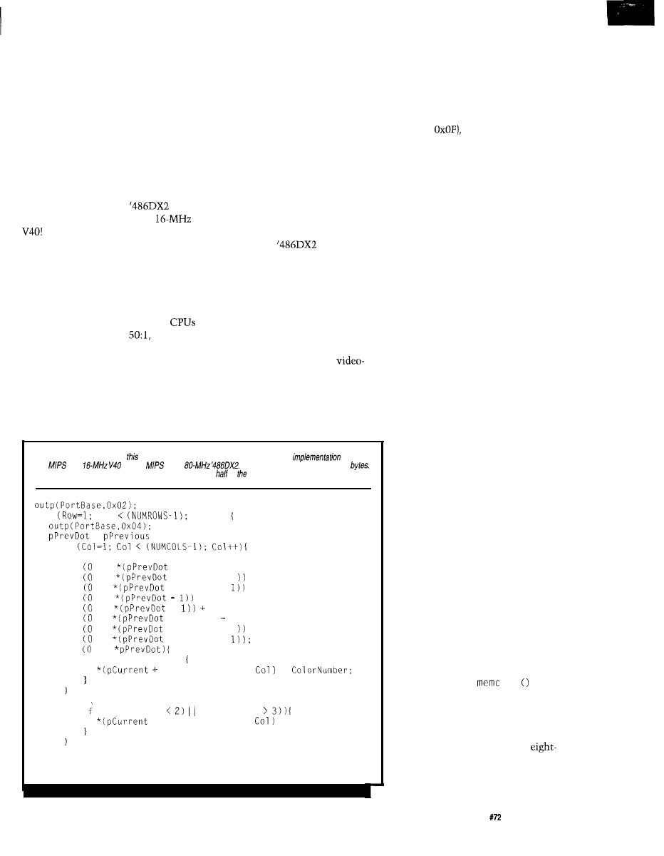
We, on the other hand, have a sim-
pler project-given a specific program,
determine how well it runs on a vari-
ety of systems. Benchmarking can
become as complex as performance
prediction, but for just one program,
we can observe what happens and find
reasonable explanations in the hard-
ware.
Last month, we saw that all the
CPU horsepower in the world won’t
help a program that doesn’t do much
computing. An 80-MHz
was
only three times faster than a
When your code is I/O bound,
don’t spend money on exotic CPU
hardware-improve the I/O channel
first.
This month, we run a program that
burns as much CPU time as possible,
while doing hardly any I/O at all. The
performance range of those same
on this task approaches
more in
line with the marketing hype.
LET THE GAME BEGIN
Selecting an appropriate program for
this column was easy. It should run on
any ‘x86 CPU, perform a vast number
of calculations on data from memory,
be easy to program, and produce inter-
esting results. I rummaged around in
my program heap and came up with
Conway’s classic Game of Life.
The Game uses a rectangular array
of cells. In principle, you update all
cells simultaneously based on their
current values.
In practice, you use two arrays: the
previous and current generations. The
algorithm reads the previous genera-
tion, computes the current generation,
displays the results, and then swaps
the arrays.
Once again, I used three Megatel
boards and my
desktop test
system. All four support VGA displays,
making video mode 13 (hex) a natural
choice.
In that mode, the screen shows 200
rows of 320 columns each, for a total
of 64,000 (decimal, exactly) pixels with
a palette of 256 colors.
Unlike most VGA modes, each
pixel corresponds to a single
buffer byte, and the program accesses
the whole array as a single, linear
chunk of memory.
Each cell in the array is either dead
or alive. A dead cell is simply a byte
Listing l--The inner loop of
simple-minded (but cache-friendly!) Game of Life
runs at
1.0
on a
and 46
on an
The nested loops fit info about 340
Process memory addresses in ascending order and reuse
of cells in each iferafion.
for
Row
Row++)
=
+ (Row * NUMCOLS) + 1;
for
Neighbors =
!=
NUMCOLS 1)) +
!=
NUMCOLS
+
!=
NUMCOLS +
+
!=
+
!=
+
!=
+ NUMCOLS 1)) +
!=
+ NUMCOLS
+
!=
+ NUMCOLS +
if ==
if (Neighbors == 3)
(Row * NUMCOLS) +
=
else
i ((Neighbors (Neighbors
+ (Row * NUMCOLS) +
= 0;
pPrevDot++;
holding a binary zero. A live cell holds
any value between 0x20 and 0x37.
Those values correspond to a pleas-
ant rainbow sequence in the default
BIOS-mode 13-VGA palette. You can
use the standard cartoon colors (0x00
through
but the rainbow is far
easier on the eyes.
Listing
1
shows the nested loops
that calculate each Game of Life gen-
eration. For each cell in the array, you
simply add the number of live neigh-
bors.
If the cell was dead in the previous
generation and had exactly three
neighbors, it will come to life in the
current generation.
If it was alive and had fewer than
two or more than three neighbors, it
will die of loneliness or overcrowding.
Otherwise, it remains unchanged.
The program increments the color
number for each generation, wrapping
from 0x38 back to 0x20 as needed.
Newly born cells contain the current
color number, making it easy to spot
their birth. Cells remaining alive do
not change colors, producing a static
background.
The calculation loops exclude a
one-cell border that holds only dead
cells. More complex versions of the
Game use toroidal arrays that connect
the top border to the bottom and the
left to the right.
You can also fill the border with
always-live cells to see how that af-
fects the results.
While Life may not be as complex
as fractal geometry, it’s certainly easier
to explain.
One pass through the inner loop in
Listing 1 requires about 100 instruc-
tions, so computing a single generation
burns slightly more than 3 18 x 198 x
100 = 6.3 million instructions.
Displaying the results involves
nothing more than copying the output
array directly into the video buffer
using the C library
py
func-
tion.
Tallying the neighbors of each cell
accounts for most of the instructions.
Listing 2 shows the compiler output
for the first two clauses of the
way addition statement in Listing 1.
I left all the compiler optimizations
and CPU selections turned off because
Circuit Cellar INK@
Issue
July 1996
59
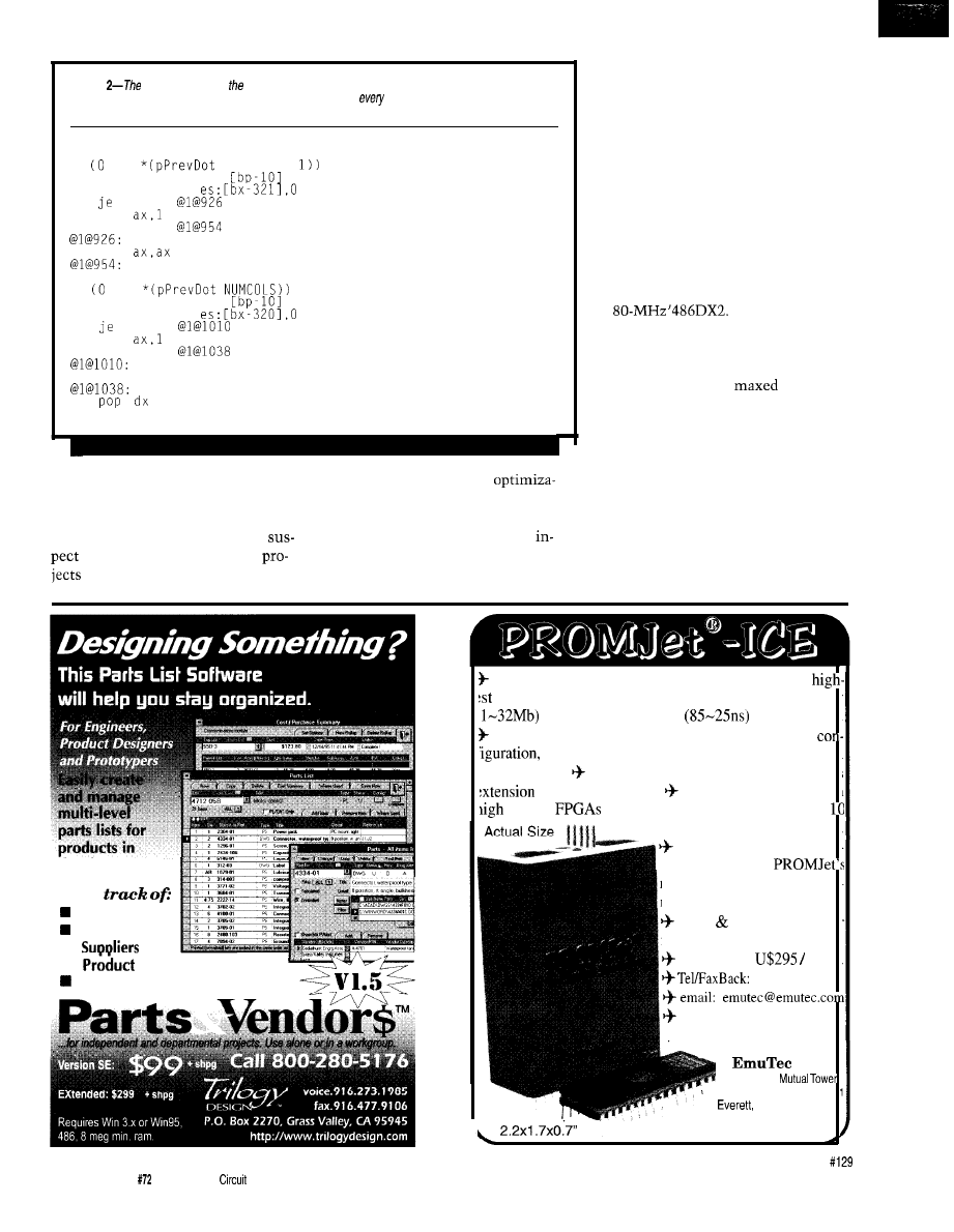
Listing
first two clauses in statement calculating the number of neighbors for each cell generate
this assembler code. A cached ‘486
CPU
averages one instruction
1.7 clock cycles,
quite good
for a
C/SC
architecture
and close to the
maximum
rate possible for a scalar processor.
; Neighbors =
; !=
NUMCOLS
+
les bx,dword ptr
cmp byte ptr
short
mov
jmp short
xor
push ax
; !=
+
les bx,dword ptr
cmp byte ptr
short
mov
jmp short
xor
ax,ax
add dx,ax
I wanted code that would run on any
In any event, optimum
of the test systems.
tion occurs much further back in the
If you wrote your own assembler
design process, well before you get to
code, you’d do much better, but I
assembly language. Down at the
most current embedded-PC
struction level, there’s only so much
use little hand-tweaked code.
improving you can do.
Many high-powered mathemati-
cians and programmers have studied
the Game of Life in the decades since
its inception. You can take advantage
of highly optimized algorithms that
compute and display generations in a
fraction of the time required by the
naive loop I’m using for this column.
If you want to live Life in the fast
lane, drop me a note and I’ll aim you at
some useful references.
With this in mind, Photo 1 shows
the timings for a single generation on
an
Calculating one
generation takes 132 ms or 48 MIPS.
That number compares quite favor-
ably with the results from last month,
where the same CPU
out at 3
MIPS running the Direct Digital Syn-
thesis loop.
Do the division: a program can run
16 times faster than another on the
same CPU!
HITTING THE CACHE
The secret to high-speed program
execution is very simple: avoid slow
operations. I/O instructions on ISA
development.
Keep
Part Specs
Drawings
n
n
and Parts Costs
Engineering Stock
Ultra compact EPROM and FLASH emulator with
download speed (l-4 Mb/S), largest memory capacity
and fastest access time
in the industry.
Other features include 3V target support, jumperless
battery backup, 128 bit bus support and external
rower supply. Fits directly into memory socket or uses
cable for flexibility. Compact design based on
density
and double-sided surface-mounted
layer PCB for added reliable operation.
ICE option allows simulta-
neous access to
memory while target is run-
ning without waitstate signal.
Plug Play drivers for
industry standard debuggers.
Priced from
MBit.
206.337.0857
www: www.emutec.com
*Fax:
206.337.3283
4
Inc
Everett
2707
Colby Av, Suite 90
WA
98201, USA
3
0
Visa&Mastercard accepted .
60
Issue
July
1996
Cellar
INK@
systems exact a severe performance
penalty, easily outweighing all other
factors for a fast CPU.
The Game of Life algorithm does
absolutely no I/O until the end of each
generation loop, freeing the CPU to do
what it does best: compute.
The two nested loops in Listing
comprise about
assembly-language
instructions that fit into the ‘486’s
KB internal cache. Even when branch-
es flush the prefetch queue, the CPU
still hits the cache with no wait states.
Surprisingly, even though 64,000
cells won’t fit into the cache, most of
the memory accesses are cache hits.
The code in Listings 1 and 2 steps
through the array in more-or-less se-
quential order, which is precisely what
the cache controller expects.
Calculating the first cell’s neighbors
causes three cache misses, one each for
Photo
each Life generation fakes
on an
caches enabled.
the leftmost cells on the three top
Copying the resulting 64,000 byfes info video buffer fakes about times longer than same copy info
rows. After the cache controller selects
system memory because video card
on
and fills three different cache lines
Even better, for the next 13 cells,
in the first row requires 2544 memory
with the first 16 bytes from those
every cell-array memory access is a
reads, only 60 of which miss the cache,
three rows, all the remaining accesses
cache hit. A rough estimate says that
That works out to a hit ratio of
are cache hits.
calculating the neighbors for 3 18 cells
ignoring all other effects.
.
C
ONTROLLER
EPROM
H
ARDWARE
S
OFTWARE
D
E V E L O P M E N T
Complete On Site
Electrical Engineering Lab
From Auto-Routing to CNC Routing to Electronic Assemblies.
Capital Electronics
is Your Best Route For Printed Circuit Boards.
P
RINTED
C
IRCUIT
B
OARDS
S
ERVICES
l
CAD
S
ERVICES
l
S
INGLE
D
OUBLE
S
IDED
l
F
AST
B
OARD
S
TUFFING
l
C
OMPATIBLE
W
ITH
A
LMOST
.
l
W
IRE
H
ARNESSES
CAD
S
YSTEMS
l
F
ROM
Q
UICK
T
URN
l
W
AVE
S
OLDERING
l
F
ROM
S
CHEMATICS OR
TO
S
C H E D U L E D
P
R O D U C T I O N
l
A
CQUISITION OF
P
A R T S
SAMPLE
PCB’s
l
L
INES
,
l
F
INAL
T
ESTING
S
E R V I C E S
l
E
LECTRICAL
T
E S T I N G
l
S
ERVICES
l
28,800
M
ODEM
l
P
RECIOUS
M
ETAL
P
L A T I N G
l
C
USTOM
E
N C L O S U R E S
For Quick Competitive Pricing or More Information,
Please Call Us Today!
852
Foster Avenue
l
Bensenville, IL 60106
( 7 0 8 ) 3 5 0 - 9 5 1 0
E-Mail:
Fax
(708) 350-9760
l
Modem
350-9761
Web Access:
Circuit Cellar INK@
Issue
July 1996
61
Accelerated Technology, Inc
Real-Tim&
Nucleus PLUS
Nucleus RTX
Real-Time Kernels
Nucleus NET
Real-Time
Nucleus FILE
Real-Time MS-DOS!
File System
Nucleus DBUG
and kernel-aware
debugger
Nucleus Real-Time
for
information and
demo
Accelerated Technology, Inc.
Post
Box 850245
Mobile, Alabama 36685
*fax:
Memory
Clock MHz
Generation
MIPS in
Clock Cycles
CPU
Caching
Time, ms
Generation Loop
per Instruction
none
6200
1.0
16
none none
1300 1100
4.9 5.8
4.9 5.1
‘486SL
internal
430
15
1.7
none
1800
3.6
22
internal
140
46
1.7
external
750
8.5
9.4
int + ext
140
46
1.7
Table l--Running a
compute-bound application on the same
as
month produces completely different
results! Notice how
caching affects generation time and
and
per
values. Computing each Life generation requires 64,000 iterations of a
loop.
In INK 70, we
saw
that a cache miss
costs -520 ns, equivalent to 40
cycle instructions for a CPU running
at 80 MHz. Photo 1 shows that the
calculations for one line take -670
so the cache-miss penalty of 30
works out to about 4.5%.
Because the entire cell array fits
into a
external cache, the situ-
ation this month is even better. Only
my
test system has an exter-
nal cache, but the results are interest-
ing.
Table 1 summarizes the measure-
ments for all the systems. The actual
time required to calculate each genera-
tion depends on the number of active
cells, so the “Generation Time” col-
umn contains the value for a particular
run.
I
rounded the measurements and
calculations to two significant figures
in honor of this uncertainty.
With both caches enabled, the
rips through a generation in
140 ms. Dividing that into the total
instructions gives about 46 MIPS, a
respectable, if somewhat artificial
figure. Dividing the clock frequency by
the MIPS number shows that the CPU
requires about
1.7
clock cycles per
instruction.
Remember that these
can
dispatch and decode only one instruc-
tion per cycle, even if their internal
pipelines hold many instructions in
various stages of execution. An overall
rate of 1.7 cycles per instruction
means that a CISC CPU like the ‘486
actually has many single-cycle instruc-
tions.
Disabling just the external cache
doesn’t change the results very much.
Even though both cell generation ar-
rays fit into the external cache, the
internal cache-hit ratio is so high that
speeding up the memory doesn’t
count.
Disabling both caches has a cata-
strophic effect on performance. With
each memory access slowed to DRAM
rates, the CPU drops to 3.6 MIPS and
22 clock cycles per instruction. That’s
only 8 % of the cached performance!
In round numbers, enabling the
external cache doubles the CPU’s base
performance and enabling the internal
cache gives you an order of magnitude.
Different benchmarks give different
results, with the Game of Life staking
out the nearly ideal end of the spec-
trum.
The Megatel
board, with a
‘486SL running at 25 MHz, clocks 15
MIPS with the cache enabled and 3.6
MIPS with it disabled. Interestingly,
this CPU requires the same 1.7 cycles
per instruction as its clock-doubling
kin.
Evidently, for this benchmark, most
of the instructions just don’t speed up
as much as you’d expect. Intel makes a
clock-doubling SL processor, but if
Megatel used it, I’d expect at least a
bullet item in the features list.
The clock-frequency difference
seems to account for nearly all the
performance difference. Multiplying 15
MIPS by
shows that the
would run at about 48 MIPS if the
memory system kept up. Converting
to 40 MHz-a more realistic
gives a respectable 24 MIPS.
I don’t have details on the Megatel
board’s memory interface. Because
disabling the cache slows the board by
only a factor of 2.6 instead of 13, I
presume that the memory is relatively
faster than that on my DX2 system. In
any event, you want the cache on all
the time!
62
Issue
July 1996
Circuit Cellar INK@
COUNTDOWN:
Comparing the Megatel
and
PC/II+ boards highlights the difference
between the ‘486 and ‘386
The
boards are, by and large, identical:
same clock frequency, same peripher-
als, same support chips. The chip set-
tings may be different, but I don’t have
any control over them!
Last month, we saw that the two
boards gave nearly identical perfor-
mance when running an I/O-bound
program. That’s no surprise, as the
ISA Compatibility Barnacles limit
these boards just as firmly as desktop
boxes.
Given a free run, though, the ‘486SL
runs three times faster than the
Intel improved the ‘486 CPU’s
hardware and microcode, speeding up
memory-address computation and
reducing the number of cycles per
instruction. If you have a
bound problem, the ‘486 runs your
algorithm much faster at given clock
frequency.
The ‘386SL on the PC/II+ board
runs at 4.9 MIPS and 5.1 cycles per
instruction. That’s only 2.2-times
faster than the I/O-bound test case,
indicating that the CPU and I/O are
more closely matched.
In effect, the CPU simply can’t run
much faster than the ISA I/O lets it. If
you are running I/O-bound code,
spending significantly less on the CPU
might be good economy.
As expected, the
has the lowest performance: an even
1 .O MIPS and, thus, 16 cycles per in-
struction at
16
MHz. Last month it ran
at 0.9 MIPS, which shows that the
instructions and I/O rates are pretty
well matched.
Having compiled all those numbers,
I turned to the dots on the VGA....
VIEWING THE VIDEO
The Game of Life produces interest-
ing patterns on the screen, which may
account for much of its popularity
some years ago. After all, what other
graphics program could you run with
just a monochrome character display?
Watching the display pointed out
another truism: not all memory is
created equal.
After computing each generation of
cells, I copied them into the VGA
buffer and the other generation array.
Listing 3 shows the two
functions that do the deed.
The version of Borland C I used
defaults to Small memory model,
which meant I allocated the two buff-
ers on the far heap. The ordinary
c
function works on the near
heap. Ah, for a flat memory model!
The
o t
functions produce
traces that measure the time required
for each memory copy. Although I
knew the copies were less expensive
than the nested generation loops, it’s
always a good idea to measure what
you’re doing.
The bottom two traces in Photo 1
show that copying 64,000 bytes into
video memory, while fast when com-
pared to the generation time, takes ten
times longer than the same copy into
system memory.
When I looked at the C library
source code,
_f memcpy
boils down
to a
REP MOVSW
instruction. Ignoring a
few tricks on ‘486
that’s as fast
as it gets.
Recall that the ‘486 CPU has a
write-through cache that caches mem-
ory reads and passes writes directly to
the external memory. In this case,
sees
a
read-hit
ratio and an agonizingly long pause for
every video-buffer write. Counting
R E P
Listing
these two
copy functions look
identical,
is dramatically slower
second because video
accesses incur many waif states. The ratio ranges from 1.41 on an
‘386 board over
on an
with both caches enabled.
update video buffer
set up new dots
POWERFUL TOOLS
REASONABLY PRICED
Supports EPROMs to
x8
to
(1 MEG)
E 4
Supports EPROMs to
to
MEG)
PC software tools
Full screen command line modes
Supports all data formats
Software configurable
access time
Power-off data retention
High-speed downloading
with error checking and correction
Non-intrusive CMOS LP design
up to 8 units -any configuration
Compact size, hard protective case
1 year warranty free software upgrades
Discounts on units
Scanlon Design Inc.
SDI
5224Blowers
Canada
J7
(902)
425 3938
(902)
4254098
8003529770
TOLL FREE IN NORTH AMERICA
Cellar
INK@
July1996
63
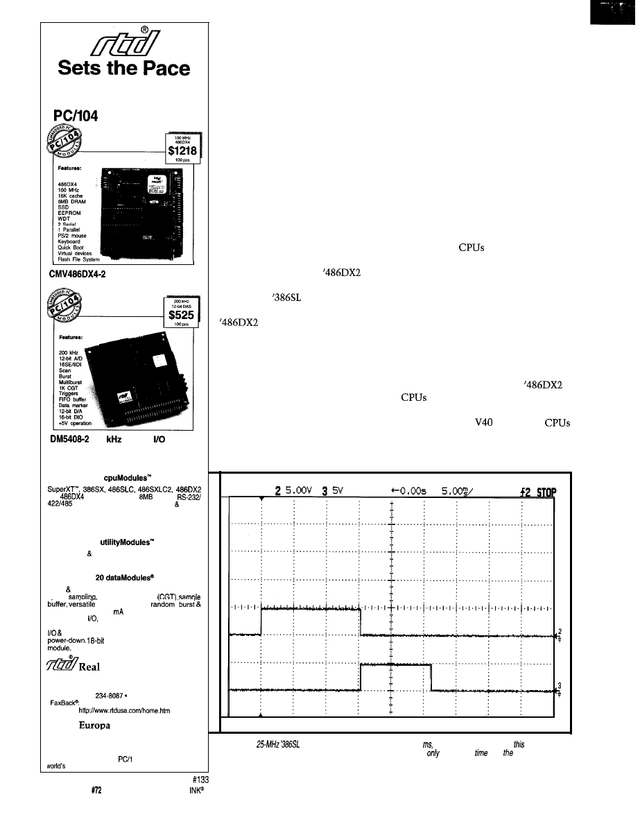
in Low Power,
High Performance
Technologies
Fully Integrated PC-AT
with Virtual Device Support
200
Analog
Module
with Channel-Gain Table
Make your selection from:
6
and
processors. SSD,
DRAM,
serial ports, parallel port, IDE floppy
controllers, Quick Boot, watchdog timer, power
management, and digital control. Virtual devices
include keyboard, video, floppy, and hard disk.
7
SVGA CRT LCD, Ethernet, keypad scanning,
PCMCIA, intelligent GPS, IDE hard disk, and floppy.
12, 14
18-bit data acquisition modules with high
speed
channel-aain table
triggers-scan,
muitiburst, DMA, 4-20
current loop, bit program-
mable digital
advanced digital interrupt modes,
incremental encoder interfaces, opto-isolated digital
signal conditioning, opto-22 compatibility, and
voltage to frequency converter
Time Devices USA
200 Innovation Boulevard
l
P.O. Box 906
State College, PA 16804-0906 USA
Tel:
1 (614)
Fax: 1 (814) 234-5218
1 (814) 235-1260 *BBS: 1 (814) 234-9427
RTD
RTD Scandinavia
Budapest, Hun&y
Helsinki, Finland
Tel: (36) 1 325-l 130
Tel: (358) 0 346.4538
Fax: (36) 1 326-6737
Fax: (358) 0 346-4539
RTD is a founder of the
04 Consortium and the
leading supplier of intelligent ISA DAS interfaces.
MO V S W as a single instruction, the CPU
runs at 37 instructions per second.
That’s unfair, of course. The MOVSW
executes 32,000 times in 26.9 ms,
running at about
1.2
MIPS. Writing
into the video buffer costs nearly as
much as accessing the I/O ports!
Photo 2 shows the ‘386SL timings.
Because this board has its VGA con-
troller on the CPU’s Local bus, copy-
ing to video memory takes only
15.2 ms, rather than 26.9 ms for the
desktop ISA VGA controller. If I had a
video Local-bus controller on the desk-
top system, the results would probably
come out the way you’d expect.
Copying to ‘386SL system memory
takes four times longer, a slowdown
from the more efficient
cach-
ing. With the ‘486 caching turned off,
though, the
actually runs twice
as fast! Of course, nobody would run a
without caching, but the raw
number is certainly interesting.
Table 2 summarizes the memory
performance for all the systems. If
your application sloshes huge arrays
back and forth, these numbers may be
more relevant than Table 1.
More likely, though, you’ll wind up
with whatever memory interface hap-
pens to be attached to the CPU you
Keep these values in mind, though,
as they put an upper limit on how fast
you can update memory-mapped pe-
ripherals.
IN CONCLUSION...
So, there you have it. Two com-
pletely different benchmark programs
that abuse the systems in two com-
pletely different ways.
Based on their results, you can fol-
low the hardware progression from a
relatively simple ‘286 to a relatively
complex ‘486 and see which features
provide the most benefit for each pro-
gram.
The faster
gain their speed,
naturally enough, by executing faster
instructions at a higher clock fre-
quency. You can extrapolate to find a
Pentium’s performance: very fast,
unless you do a lot of I/O. Then, re-
gardless of how fast the CPU might be,
it spends far too much time just wait-
ing around.
the job!
The Game of Life uses only integer
arithmetic, leaving the floating-point
hardware on the ‘486SL and
completely unused. If your ap-
plication depends on real-number
calculations, the
and ‘386SL
are certainly not the right hammers for
need for the rest of the job.
Photo 2-A
computes Life generations
in -1800 far too long
for the scale of
scope shot.
However, copying the results info the Local-bus video buffer requires
40%
more
than same operation
info system RAM.
66
Issue
July 1996
Circuit Cellar
Memory
copy to
Clock
Video Buffer
copy to
copy to
Video
CPU
Caching MHz
Memory
Slowdown
ms
ns per word
Memory
ms
ns per word
Ratio
none
‘386SL
none
117
3700
45.6
1400
2.6
15.2
480
10.8
340
1.4
none
16.4
510
9.64
300
1.7
‘486SL
internal
15.8
490
5.30
170
3.0
none
31.3
980
19.5
610
1.6
internal
27.6
860
6.44
200
4.3
external
31.0
970
5.08
160
6.1
int + ext
26.9
840
2.61
82
10
Table 2-Somewhat
surprising/y,
memory and video accesses run
faster on the
embedded-PC boards than on the
turns out that the Local-bus video
controllers on the
boards
outperform an ISA desktop VGA
board.
Conversely, if your application does
can’t twiddle the knobs, push the
Oh, yeah, your article. Guess what?
lots of I/O backed by relatively little
calculation, splurging on a
won’t buy you much beyond a warm
feeling that you’re covered when the
specs change.
In any event, we’ve certainly pinned
down the performance extremes.
You’ll be hard-pressed to find better or
worse performers!
WINNING THE DESIGN CONTEST
One harbinger of the sleet season
around here is the arrival of a huge
stack of INK Design Contest Entries. I
spread the folders all over the floor,
read through their contents, sort them
several ways according to the rating
criteria, and pick the best of the lot.
Some entries arrive without a scrap
of explanatory text. All I see is a sche-
matic, perhaps a program listing, and
maybe a photograph or two. With no
background, I can’t tell what the pro-
ject is, what it does, or why I should
care. It might represent the most chal-
lenging project in the stack, but if
somebody else gives a better explana-
tion, well....
All this takes days of reading and
shuffling, but the winner usually be-
comes apparent during the first pass.
Every year, it seems, all the judges
independently agree that one entrant
got everything right. The contest then
boils down to ranking the others.
Next, if you’re doing something
completely off the wall, give me a
chalk talk on the technical back-
ground. For example, Rick May figured
power consumption by multiplying
current times voltage in a quad
isolator. He included the original de-
sign description, sparing me the
trouble of figuring out how it worked,
and eliminating the risk that I might
not bother.
Conversely, another entrant gets
nearly everything wrong. The project
may be interesting, the work may be
technically adept, but the contest
entry doesn’t stand a chance. Strangely
enough, all the judges seem to agree on
that one, too. A single photo clipped to
a program listing does not a winning
contest entry make.
If the schematic isn’t trivial, ex-
plain what’s going on. You can assume
I know electronics pretty well, so you
needn’t explain the obvious. Similarly,
describe just the really tricky sections
of the software, as I’m not up to speed
on every CPU in the world.
To put this on a personal level,
think of me sitting across a table from
you with your project between us.
Your assignment: tell me about your
new widget, as best you can.
The first thing I want to know is
what your project does
what problem it solves. You are thor-
oughly familiar with what you did, but
remember, I’ve never seen it before.
Worse, your contest entry just de-
scribes the hardware and program. I
Don’t be afraid of diagrams showing
how things work. Very often, one sim-
ple, hand-drawn sketch makes a page
of text perfectly obvious.
Conversely, don’t bury me in mean-
inglessly detailed flowcharts of your
code. Just make the higher levels clear;
the rest follows.
You needn’t spice up your narrative
with humor, shaggy-dog stories, or
fancy prose. Make every word, every
schematic, every figure explain some-
thing useful. Convince me that you’ve
done something really neat. Save the
stories for your article.
tons, or watch the screen. If you don’t
mention something, I’ll never discover
it.
That explanation forms the basis for
the INK article telling everybody else
how you took the top prize! If you can
explain it to me, you can explain it to
them!
Go for it!
RELEASE NOTES
LIFETIME.EXE shouldrunonany
stock DOS PC with a VGA-compatible
video interface. L I F EC . E X E disables
the ‘486 on-chip cache using, naturally
enough,
instructions that
crash other systems. Pick the appropri-
ate one for your situation.
The programs produce blips on the
system’s highest-numbered LPT port.
You can hitch up a scope to track ex-
ecution times through various sections
of code. Press any key (other than the
shifts, OK?] to return to DOS.
Next month: tuning up.
q
Ed Nisley
as Nisley Micro
Engineering, makes small computers
do amazing things. He’s also a
member of Circuit Cellar INK’s
engineering staff. You may reach him
at
or 74065.
PC/II+,
Megatel Computer Corp.
125 Wendell Ave.
Weston, ON
Canada
(416) 2452953
Fax: (416) 2456505
416
Very Useful
417 Moderately Useful
418 Not Useful
Circuit Cellar INK@
Issue
July
1996
67
Hard Facts
About
Soft Ferrites
Jeff Bachiochi
work on the theory of magnetism. For
the first time, it was suggested that
Earth itself was one giant magnet.
Invisible lines of force leave the
north magnetic pole and reenter the
earth through the south magnetic pole.
Luckily, civilization prospered around
the equator and not the poles where
the compass was useless (either point-
ing down in the north or, worse yet, up
in the south).
It wasn’t until 1820 that a Danish
physicist, Hans Oersted, observed a
relationship between magnetism and
electricity. A compass needle in close
proximity to a current-carrying wire is
attracted toward the wire.
From this experiment came the
“right-hand rule.” When the right
hand is held in the hitchhiker position
with the thumb pointing in the direc-
tion current flows through a conduc-
tor, the fingers point in the direction of
the magnetic field created by the cur-
rent flow.
Ten years later, Michael Faraday
created an electric current by passing a
magnet near an electrical conductor.
He summarized the phenomenon as:
l
moving electrical charges produce
magnetic fields
l
magnetic fields exert forces on mov-
ing charges
l
changing magnetic fields cause elec-
trical currents to flow
At some point during our elementary
or secondary school careers, most of us
have demonstrated these invisible
lines of force by sprinkling iron filings
on a piece of paper held above a mag-
netic source.
The mathematical theory describ-
ing the disturbances caused by moving
magnetic fields and electrical charges
was published in 1864 by James Clerk
Maxwell. His experiments led to the
discovery that the disturbances can be
treated as wave motion and that they
travel at the speed of light (3 x
m/s).
A magnetic field is set up by elec-
tric current flowing through a conduc-
tor. It gets stronger if either current
increases or the conductor is looped so
that the magnetic fields produced are
cumulative.
This arrangement created the first
coil (solenoid) and led to the discovery
of electromagnetism. The ability of a
magnetic field to strongly attract iron,
cobalt, or nickel was named
netism.
As you remember from chem-
istry, ferro comes from the Latin for
“relating to iron.”
What’s so special about these ferro-
magnetic materials? It begins with the
atomic structure of materials.
The negatively charged electrons
circling the nucleus of an atom form
shells as they whiz around at different
energy levels. Each electron can have a
mate or not depending on whether an
odd or even number of electrons are in
the shell.
Electrons having a mate often have
opposing spins, and the magnetic ef-
fects of the opposing charges cancel.
Single electrons can be coaxed into
spinning in the same direction by an
external magnetic field. When this
happens, the material becomes magne-
tized, and the magnetic field is en-
hanced.
These “soft” magnets lose most of
their magnetism when the external
magnetic field is removed because the
single electrons are no longer working
together. Internal forces enable “hard”
magnets to retain their magnetism
unless affected by an external stimulus
like heat or a hard whack.
Not all magnets are composed en-
tirely of metal. Lightweight ceramics,
known as ferrites, have many of the
same properties.
68
Issue July
1996
Circuit Cellar INK@
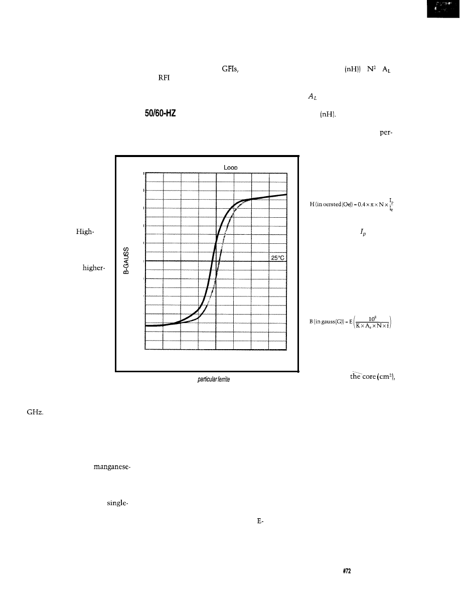
Let’s take a look at these materials
and see what makes them so useful.
Inductance for a particular core
material is calculated with the for-
mula:
SOFT CERAMIC
Although magnetite, a naturally
formed magnetic mineral, is found in
plentiful deposits in Asia, it wasn’t
until 1945 that soft magnetic materials
could be produced in the lab. These
materials were produced in the Neth-
erlands for commercial applications by
J.L. Snoek of Philip’s Research Labora-
tories.
Many of today’s products would not
be possible without the use of ferrite.
Electronic applications include power
transformers and chokes, pulse- and
wide-band transformers,
and EM1
and
suppression.
Let’s look at some of these in more
detail.
L (in nanohenries
= x
POWER TRANSFORMERS
Ferrite-core power transformers
look very much like their counterpart,
where N equals the number of turns of
wire, and equals the inductance
index listed for each size and composi-
tion of ferrite
The inductance
increase of a ferrite core over an air
core for the most part equals the
Ferrites are homogeneous
ceramic materials made up of
various oxides, primarily
iron. Their composition
hasn’t changed much over
the years, but process control
has improved their purity.
the laminated-core transformer. The
Hvsteresis
meability of the material being used.
The peak magnetic field
strength is based on the
current passing through the
conductor and is measured
by:
Ferrite materials are found
in almost every electronic
product used today.
electrical resistivity dramati-
cally reduces the eddy cur-
rent losses associated with
metal laminations. In
frequency applications, this
resistivity is even more im-
portant as the losses increase
with the square of the fre-
quency.
The production process of
ferrites lends itself to special
shaping by pressing, extrud-
ing, and/or grinding tech-
niques. And, the material is
efficient. High magnetic
permeability concentrates
and reinforces the magnetic
5000
4000
3000
2000
1000
0
1000
2000
3000
4000
5000
2.0
1.5
1 .o
0.5 0
0.5
1.0
1.5
2.0
H-OERSTEDS
Figure l--The
hysteresis loop
for this
material
shows
a tendency
to
remember
a small amount of magnetism once the field is reduced to zero.
field better than any other
class of magnetic material from audio
to 1
turns of wire, and
f
is the
frequency [Hz).
where N equals the number
of turns of wire, is the
peak current (A), and 1, is the
effective path length of the
core (cm).
Another important quan-
tity is the peak flux or maxi-
mum flux density created in
the core material. You calcu-
late this quantity by:
The mix of materials used to pro-
duce the ceramic shapes varies to
achieve different characteristics. These
features are pretty much a tradeoff of
high permeability for that of higher
electrical resistivity. The
zinc ferrites have the highest perme-
ability, while the nickel-zinc ferrites
have the highest electrical resistivity.
Most ferrite is produced as
or multiholed cores. These are toroids
and beads. However, ferrite is made in
many other shapes such as rods, pot
cores, and tuning slugs for variable
inductors.
high electrical resistivity of ferrite
reduces core heating, and the high
permeability helps to concentrate
magnetic flux, reducing stray magnetic
fields. Designs, however, are limited
by core saturation or heating due to
core or winding losses.
Iron-core laminations are usually
produced in the shape of an E-hence
the name E-core. The E-shapes are
inserted into a bobbin from alternating
sides to build up a solid figure-eight
core around the bobbin. Ferrite is eas-
ily molded into E-shapes. Only two
shapes are necessary to complete a
core, eliminating the need for iron
laminations.
where E equals RMS voltage,
K is a constant depending on
wave shape (4.44 for sine
waves), A, is the cross-sec-
tional area of
N stands for the number of
The peak flux density is important
because this must remain within the
linear part of the B/H hysteresis loop
for the material to remain unsaturated.
The graph in Figure 1 shows the
relationship between magnetic field
strength (H, in Oe) and the magnetic
flux density (B, in G). The hysteresis
loop is created by the flux-density
remanence or flux density remaining
once the applied magnetic field
strength is reduced to zero.
POWER INDUCTORS
Although transformers may be
wound using toroid forms, you’re more
Circuit Cellar INK@
Issue
July 1996
69
DOMESTIC NEWSSTAND PRICE
Upcoming 1999 issues will feature:
August
Robotics
September
Embedded Programming
October
Fuzzy
November
Digital Signal Processing
December
Graphics Video
our always-popular
BONUS SECTIONS
the Embedded PC market and
Home Automation Building Control
One year (1 issues) for only $21.95 (U.S.)
$31.95 Canada Mexico, $49.95
non-U.S. addresses
(U.S.
drawn on U.S. bank)
n
n
IT’S EASY TO SUBSCRIBE!
Tel:
975-2199
l
Fax:
l
971
or visit our web site at:
likely to find these donut shapes being
used for chokes.
For low-power inductors [less than
100 G), the coil’s “Q” is determined by
the material’s permeability and loss
factor (tan
This also relates to the
wire size
inductance (L), and fre-
quency (Hz).
Loss factors increase and permeabil-
ity decreases as frequency goes up.
However, they are nominally flat at
less than 1 MHz. As power increases,
so will the hysteresis, winding, and
core losses. But, in general, these are
less than those chokes of iron-lamina-
tion construction.
If there is a DC component to the
circuit current, as in power-supply
designs, that DC current creates a bias
magnetic field. If this field is signifi-
cant, it alters the available saturation
level for the AC current.
This peak magnetic field strength
should be calculated separately. The
overall field strength can be reduced by
raising the inductance (fewer turns) or
by lengthening the magnetic path
length (larger diameter toroid). Slotting
the toroid (providing an air gap) also
lowers the permeability.
CURRENT TRANSFORMERS
The primary coil of current trans-
formers has as few as a single turn.
Toroids used as current transformers
may require the primary coil to simply
pass through the center of the toroid.
Here, the transformer’s primary coil
is not the load but a series sensor for
current. As in a regular transformer,
the conductor’s current produces a
magnetic field (albeit a small one since
the number of turns is small), which is
collected by the high-permeability
core.
The secondary coil’s turns ratio is
large to create a small voltage propor-
tional to the primary conductor’s cur-
rent. Current transformers are used as
protecting AC outlets in the
bathroom and kitchen.
FERRITE BEADS
An economical method of attenuat-
ing unwanted high-frequency noise is
to create an RF choke by placing a
ferrite bead on the conductor. you’ve
probably seen big hunks of ferrite
Issue July
1996
Circuit Cellar
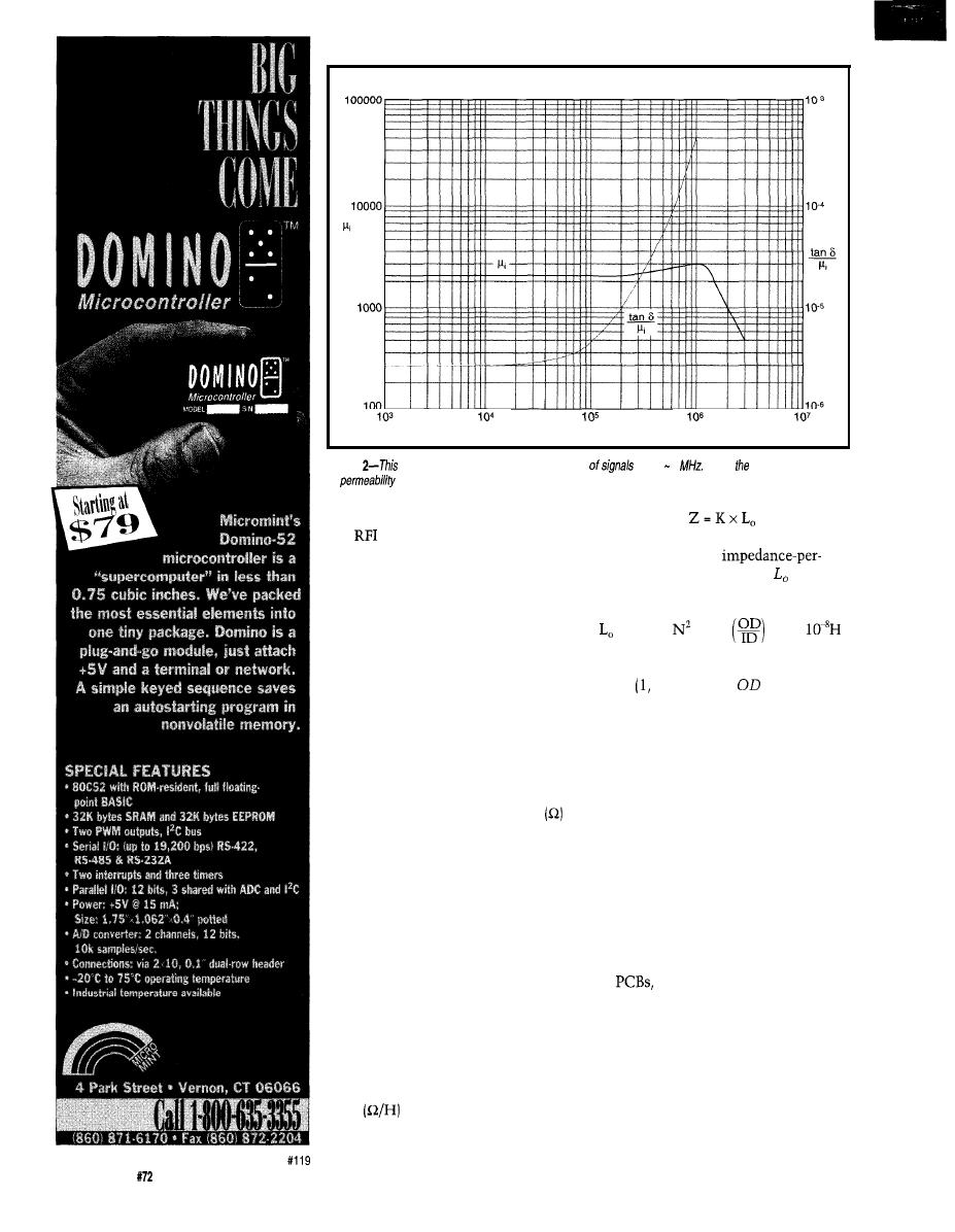
Initial Permeability and Loss Factor vs. Frequency
Frequency (Hz)
Figure
ferrite
material is designed for attenuation
above 1
Notice effects of frequency
on
and loss.
placed on video cables to reduce EM1
and
emissions.
At low frequencies, the conductor
(with a ferrite bead) looks like low
impedance. But, at higher frequencies,
its high impedance chokes off RF.
At low frequencies, the component
[conductor and bead) presents a rela-
tively small inductance whose reac-
tance can be neglected.
Permeability remains fairly con-
stant up into the megahertz region, but
rises slightly before falling off dramati-
cally (see Figure 2).
The loss factor grows rather linearly
over the same range. It is the rising
loss which adds series impedance
to the falling inductive reactance and
absorbs the higher unwanted signals.
In selecting the right bead for your
application, note where attenuation is
necessary and choose the material
most effective for that range.
In general the higher-permeability
materials begin attenuation at lower
frequencies (approximately equal to 1
MHz), while the lower-permeability
materials begin attenuating a decade or
two higher.
Using the specific charts for the
various materials, one can pick off the
impedance-per-unit-of-air-core induc-
tance
and substitute this into
the formula:
where K equals the
unit-of-air core inductance. is deter-
mined by:
= 0.046 x x log,,
x Ht x
As with all ferrite, the temperature
affects each material differently. Refer
where N stands for the number of
to individual temperature specifica-
turns in this case),
is the out-
tions if the equipment is to be oper-
side diameter of the bead (mm), ID is
the inside diameter of the bead (mm),
and Ht equals the height or length of
ated at elevated temperatures.
the bead (mm).
And, as with any transformer, DC
bias decreases the effective impedance.
This decrease can be as much as 50%
with a field strength of only a few
oersteds.
Since some beads are placed directly
on
the resistivity of the material
is important. High-permeability mate-
rials (manganese-zinc) generally have
low resistivity (100 Q/cm). The beads
act as conductors, and circuit traces
must be placed so that the beads are
not shorted out.
An alternative solution is to use
beads that come processed with an
72
Issue
July 1996
Circuit Cellar INK@
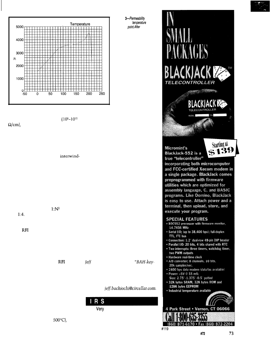
Initial Permeabilitv vs.
Figure
in-
creases
with
up to
its
Curie
this, if falls
dramatically.
loses
all magnetic
properties.
Temperature (“C)
insulating coat.
Nickel-zinc ferrites
have much higher resistivity
but the tradeoff is lower perme-
ability.
The effect reverses
as the material regains
its properties once
temperature reduces.
In general, permeability increases as
the temperature rises, although each
material has its own characteristics as
shown in Figure 3.
Multihole cores increase the imped-
ance via multiple turns through the
same core. The number of turns used
here is generally low and most effec-
tive at lower frequencies, as
ing capacitance increases with the
number of turns.
Baluns are special transformers
using a twin-holed bead. They are
usually used for impedance matching
where two turns (the center tap being
grounded) form the unbalanced con-
nection. One winding and centertap
form the second balanced connection.
The impedance ratio is
or, in this
case,
Twin-hole beads are also used as
common-mode chokes. Much con-
ducted
is common-mode. This is
reduced by applying the choke so the
signal and return paths on the input
side both go on the same core, wound
in the same direction.
The output side sees-or, better yet,
does not see-the common
that
cancels. Yet, the important signal
slides on through.
ENVIRONMENT
Since ferrites are inert ceramics free
of any organic substances, their perfor-
mance is not degraded by most envi-
ronments (including heat up to a few
hundred degrees Celsius). Above the
Curie temperature (which varies in
materials from 120°C to
ferrite
SURFACE-MOUNT COMPONENTS
You’ve undoubtedly noticed the
proliferation of surface-mount prod-
ucts. Most would not be possible with-
out today’s SMT ferrite inductors.
Most inductor manufacturers have a
complete line of SMT parts.
Power products, where heat is of
concern, can be shrunk due to the
reduced losses within ferrite cores.
And, ferrite is much better at contain-
ing stray-magnetic fields than lami-
nated-style transformers.
Because manufacturers continue to
improve materials and process control,
new uses for ferrite will continue into
the next century.
Remember core memory? Well, try
to forget it. Although ferrite is being
used more and more, I doubt we’ll see
a renaissance in the use of ferrite for
improved memory products.
q
Bachiochi (pronounced
AH-key”) is an electrical engineer on
Circuit Cellar INK’s engineering staff.
His background includes product de-
sign and manufacturing. He may be
reached at
419
Useful
420 Moderately Useful
421 Not Useful
Circuit Cellar INK@
Issue
July 1996
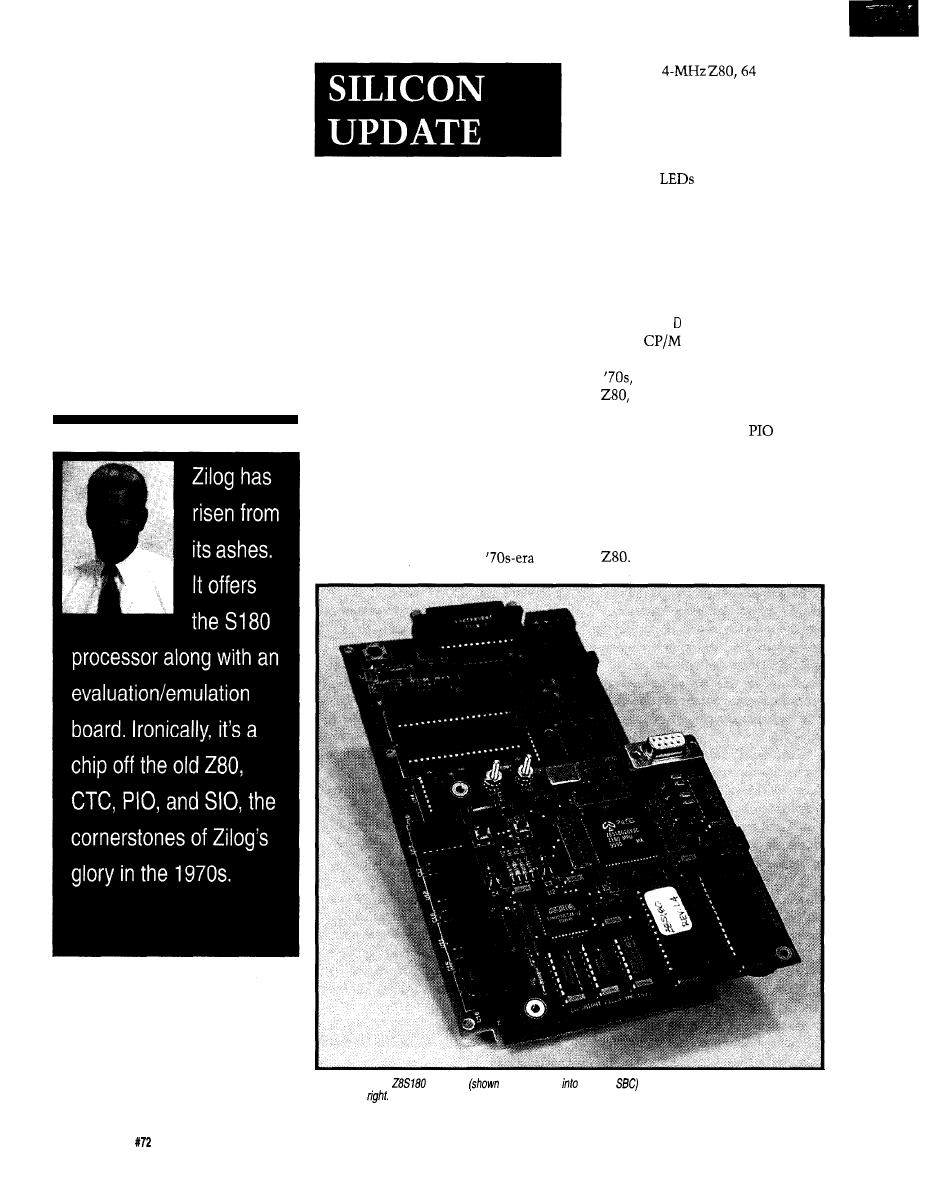
Flight
of the
Phoenix
Tom Cantrell
0
ake a close look
at the logo on a
Zilog chip. Though
admittedly abstract, it
depicts a Phoenix, also known to those
up on their mythology as the bird that
rose from the ashes.
It’s rather fitting as far as logos go,
given the history of the company. I
must admit to a personal interest in
this, having fond memories of the
early days of microprocessors and
personal computing. Indeed, shoved in
a closet is my old IMSAI (a
“PC”) with a
KB of
RAM, and mighty 8” floppies.
Just for kicks, every now and then, I
fire the old bird up. Sure, I have to wait
a few minutes for the chips to warm
up, but soon I’m flipping switches and
scanning the
of that wonderful
front panel (wish they still had ‘em).
Stop-Reset-Examine-Run is re-
warded with a satisfying clanking
sound you don’t hear anywhere but at
a machine shop these days as the 8”
floppy pounds into action. Surprisingly
quickly, the familiar A> prompt ap-
pears. I type in
I R
just like now,
except it’s
instead of MS-DOS.
Yeah, Zilog was flying high in the
late
not just on the strength of
the
but on a critical triad of pe-
ripheral chips-the CTC (counter/
timer), SIO (serial I/O), and
(paral-
lel I/O).
Each peripheral either matched or
exceeded its equivalent from Intel and
Motorola. Like the tail wagging the
dog, the attraction of the peripherals
often tipped a CPU decision in favor of
the
Photo
l--The
emulator
here plugged
a target
may look
a little awkward, but if works and
the price is
74
Issue
July 1996
Circuit Cellar INK@
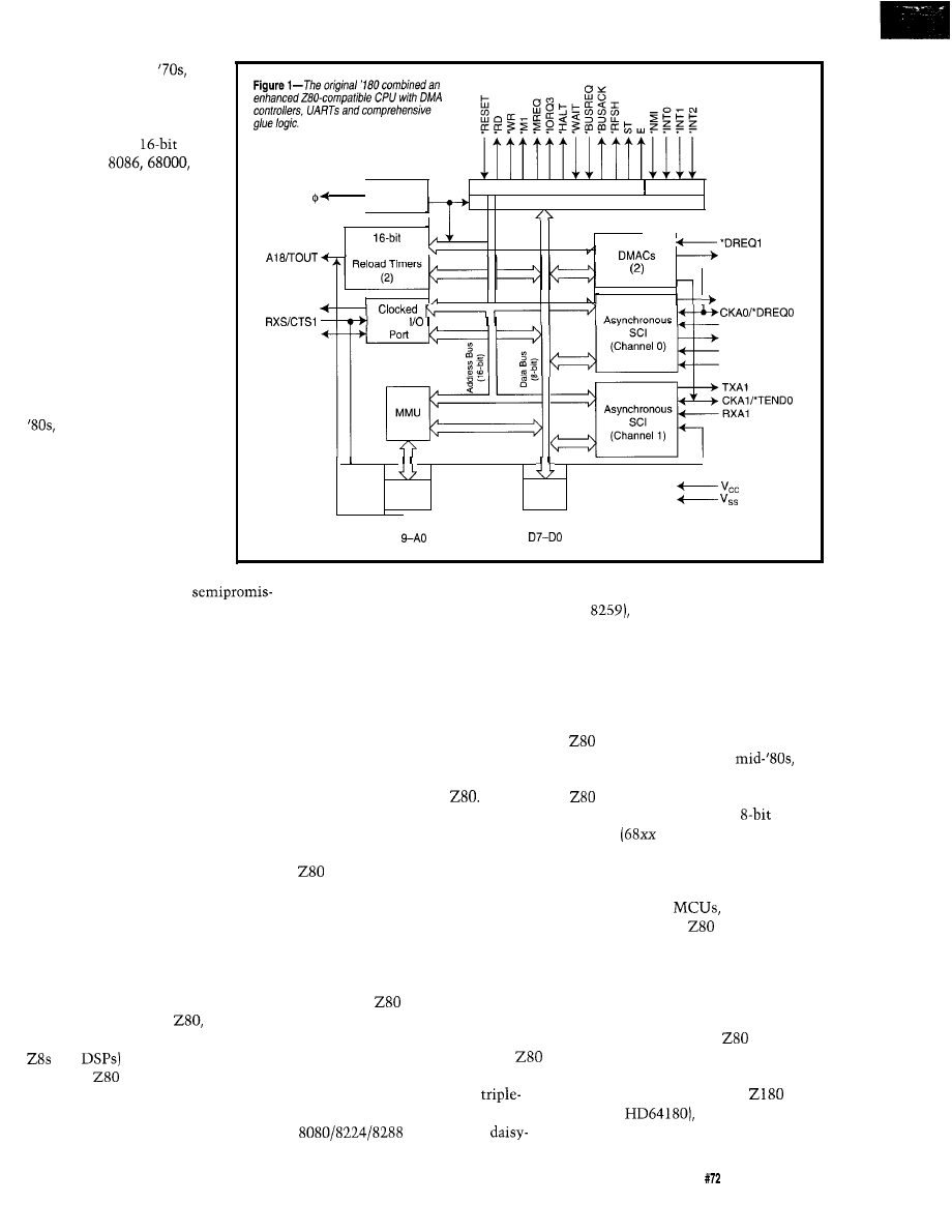
Timing
Bus State Control
Interrupt
Generator
CPU
Programmable
‘TEND1
t
TXAO
TXS
Serial
RXAO
CKS
‘RTSO
‘CTSO
‘DCDO
I
Chips were announced
but not delivered, perhaps
not surprising given that
employee turnover was at
revolving-door level. The
UNIX workstations were
ing, until an outfit called Sun came
along and spoiled the party. Like an
over-the-hill champ getting pounded,
it was sad to watch.
Address
Data
Buffer
Buffer
Al
programmer’s model and instruction
chain interrupt scheme (i.e., no need
set that persists largely unchanged
for
DRAM refresh, and so on.
By the end of the
however, the first whiffs of
smoke could be detected as
Intel, Motorola, and Zilog all
geared up for the
battle
between the
and 28000, respectively.
Despite competitive technol-
ogy, Zilog was no match for
the goliaths-it was kind of
like being an ant in a boxing
ring.
Certainly, once the PC
and Mac established them-
selves, Zilog, having burned
the candle at both ends, was
little more than toast. While
most businesses and semi-
conductors boomed in the
Zilog stumbled along
under the tutelage of Exxon
(it didn’t make sense then
either).
Finally, in a classic example of the
destruction and creation of capitalism
(i.e., the corporate equivalent of a call
to Dr. Jack), the bankers stepped in,
and in 1989, the company was taken
private (i.e., kind of like firing your
boss).
Since then, a “new” Zilog has risen
from the ashes of the ’80s with in-
creasing sales and healthy profits in
the ’90s. Sure, they’ll never be an Intel
or Motorola, but that doesn’t mean
they can’t have a decent business and
deliver some neat chips just the same.
FLASHBACK
It’s somewhat ironic that, nearly
twenty years later, Zilog still counts
on descendants of the
CTC, PIO,
and SIO as a cornerstone (along with
and
of their business.
A brief
history for those of you
who weren’t around (or can’t remem-
ber) starts with the introduction of the
8080 by Intel, defining the core of the
today.
Back then, things were pretty
loosey-goosey on the legal front, so a
bunch of the 8080 team simply went
across town and formed Zilog. Wheth-
er due to lack of legal savvy, ‘x86 dis-
traction, or simple fairness (Intel did
much the same thing to Fairchild),
Zilog was allowed to sell their en-
hanced 8080 clone, the
For customers who’d bought into
the 8080 but didn’t relish having 16
bits crammed down their throats, the
was welcome indeed.
First, the programmer’s model was
upgraded with a number of features,
(index registers, block-move instruc-
tions, and alternate register set). De-
pending on the applications, some of
these were useful, some not so. But
overall, the
struck a good balance
between enhancement and compatibil-
ity.
For the hardware designer, the
was a vast improvement over the 8080.
Single +5-V versus the 8080
power supply, single chip versus the
trio, built-in
Intel made a belated and, consumed
as they were with the forthcoming
‘x86 campaign, half-hearted response
with the 8085, but few chose it over
the 280.
Of course, this rosy time for the
was also the beginning of the end
for Zilog. By the early- to
they were well into the Dark Age. The
sputtered along on autopilot, ef-
fectively falling behind as
com-
petitors
and 805 1) moved ahead.
Fortunately, Hitachi stepped into
the breach with the HD64 180. Taking
inspiration from both the Intel ‘186
and single-chip
the ‘180 com-
bined a freshened
CPU core with a
rather extensive complement of glue
and I/O logic. The ‘180 kept up with
competitors and achieves notable suc-
cess to this day in modems, faxes, and
printers.
The ‘180 carried the
torch
through the tough times, and now
Zilog has picked up the ball again.
Besides the circa-‘80s stock
(i.e.,
same as
they’ve concen-
trated on fine-tuning the CPU for both
Circuit Cellar INK@
Issue
July
1996
75
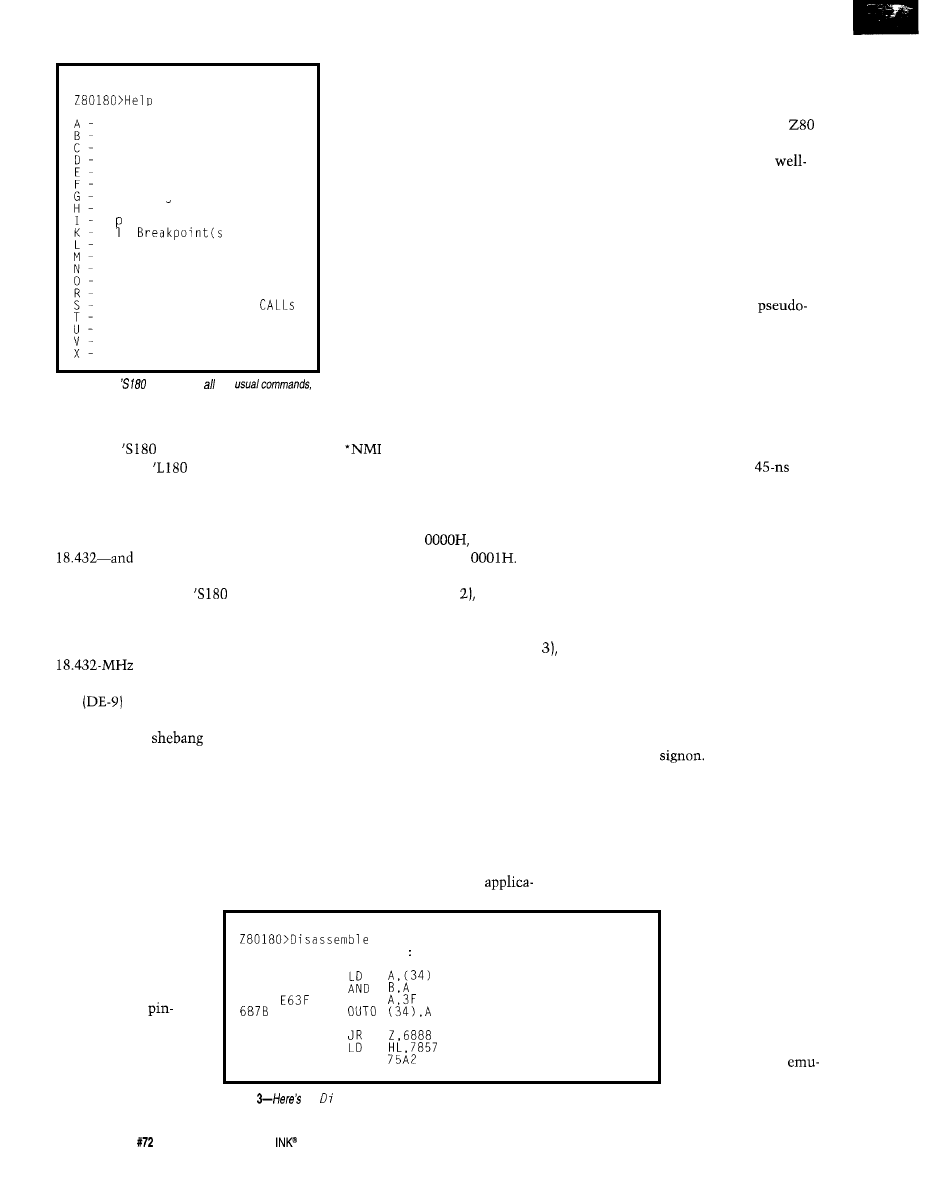
Zilog Z80180 Monitor V. 1.4
Alter Memory
Set or Show Breakpoints
Compare Memory Data
Display Memory Data
Edit/Display I/O Data
Fill Memory
Go to Proaram
Help
In ut Byte From I
Ki 1
Load Hex File
'0 Address
Move Memory to Memory
Change Serial Data Rate
Output Byte to I/O Address
Display/Alter Registers
Step (over Subroutine
Step (into Subroutine CALL
S
Disassemble Instructions
Display Version of Monitor
examine the MMU
Figure
2-The
monitor has the
which includes the handy disassembler shown in action in
Figure 3.
speed (the
up to 33 MHz) and
low power (the
at 3.3 V).
CHIP OFF THE OLD BLOCK
Knowing that the best way to check
out the emulator was with a known
good system, I rummaged through my
board stash to find the ‘180 SBC that
was upgraded from 9.216 to 18.432
MHz in the “I’m 18.432” article. Yes,
there it is, the one with the
EPROM and ‘ALS decoder to handle
the higher speed.
I
covered the ‘S
180 you see
in Fig-
ure
1
in an earlier article (INK 29, “I’m
I Like It”). Recently, a
press release from Zilog announced a
low-cost (under $200)
evaluation
and emulation board.
and
(nonmaskable interrupt).
Changing the CPU clock rate re-
quires soldering a new crystal and
rebuilding the EPROM. The emulator
traps to the monitor when executing
an instruction at
so you’ve got
to ORG your programs at
The setup you see in Photo 1 con-
sists of a “brain” that’s essentially an
‘S
180
SBC including
EPROM, RAM, PLD, and RS-232 inter-
face
and a PLCC plug-in pod
that mates to the bottom of the brain,
with the whole
dropping into
an ‘S 180 CPU socket.
The monitor contains the usual
commands (see Figure allowing you
to look at and manipulate memory,
registers, and I/O. One helpful addition
is a simple disassembler (see Figure
handy for quick-and-dirty patchwork.
As expected given the bargain price,
there’s no special hardware for break-
points, which are thus limited to in-
structions in RAM.
Being the cautious type, before
lashing the whole setup together, I
verified the SBC still worked-good,
no rusty transistors.
Next, I connected the emulator
brain alone (i.e., not plugged into the
SBC) to the PC RS-232 port, running it
as a stand-alone EV board. The emula-
tor DE-9 is female which required a
male-male adapter to work with my
DE-9-to-DB-25 adapter gadget.
Meanwhile, the other end of the
connectors that mate brain and pod
serve double-duty, emerging as pins on
top for connecting a logic analyzer.
That’s OK though, since the unit
includes a socket for emulation RAM.
It’s shipped with an 8 K x 8 RAM, but
can handle a larger chip within the
limit imposed by the 28-pin socket
[i.e., 32 K x 8). This handles the typical
less-than-64-KB three-chip system, but
proves confining for larger
Powering the emulator up and hit-
ting carriage return, I was greeted with
the monitor
Excellent! Other
than the cable sexual-identity crisis,
nary a single RS-232 hassle.
Admittedly, the form factor calls for
a fair amount of head and shoulder
room for installation. Otherwise, it’s a
quite workable solu-
tion, especially given
the bargain price.
Feeling rather pleased with my
progress, I plugged the emulator into
the PLCC adapter pod and then the
‘180 SBC. Making one last wiring and
pin-l check, I hit the power switch.
Like other low-cost
emulators, this one
works by effectively
constructing a
compatible single-chip
CPU with ROM and
RAM running a moni-
tor program that talks
to the PC via RS-232.
Starting at (just CR = From PC): 6875
Number of Instructions 8
6875 E D 3 8 3 4
IN0
6878 47
6879
ED3934
687E CB78
BIT 7,B
6880 2806
6882 215778
6885 CDA275
CALL
Figure
the sass emb 7 e command in action.
76
Issue
July 1996
Circuit Cellar
Thus, it doesn’t have fancy real-
time trace (you can use a logic
analyzer instead), complex break-
point, or nonintrusive debug fea-
tures. Also, “soft” emulators of this
ilk invariably impose some restric-
tions on the target design.
For instance, the emulator
switches control between the local
and target memory by gating the
l
MREQ (Memory Request) line to
the pod. Thus, the target must
qualify its own memory-enable
logic with *MREQ (which is typical
practice).
Also, there’s no easy way to
debug an application’s use of a few
core functions required by the emu-
lator, such as a couple of the RST
vectors (restart instructions are for
breakpoints and monitor services)
tions, which should probably use in-
dustrial-strength tools anyway.
When it comes to software, need-
less to say, there’s no shortage of
tools. Besides quantity, a lot of it is
very good quality, having been
debugged and optimized over the
years. I don’t know about you, but it’s
comforting to use software that hasn’t
had a bug since disco!
If you’re new to the ‘180 and don’t
already have favorite tools, the kit
includes a decent PC-based assembler
(macros, expressions, lots of
ops), linker, assorted object-file utili-
ties, and a simple terminal program.
LOST WEEKEND
Actually, it was
only Saturday night
and Sunday morning,
but given chores and
familial interface du-
ties, it pretty much
shot the whole thing.
Of course, the
lator/SBC setup was
dead, the screen mute
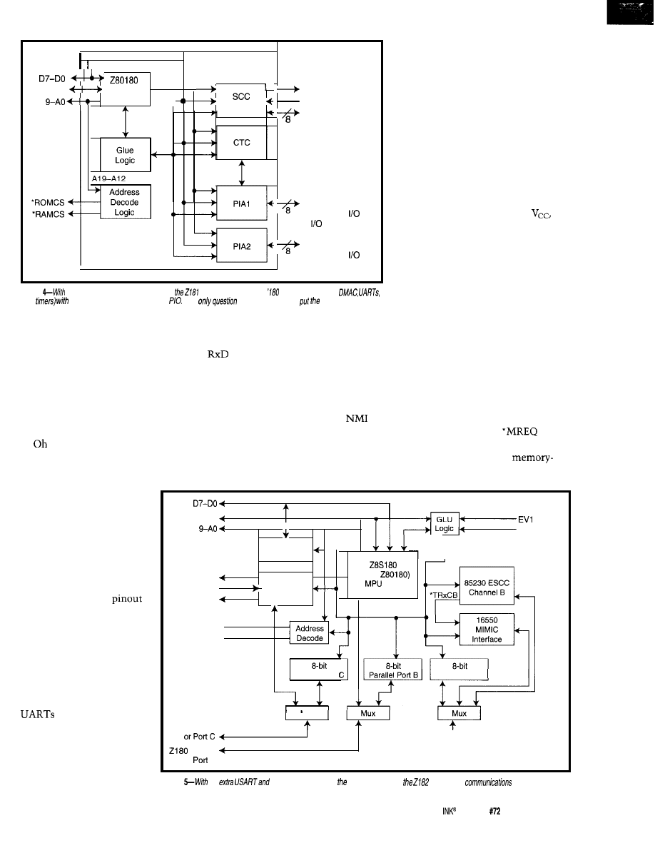
Control
Compatible 4
Al
Core
(1 Channel)
T
X
Data
Rx Data
Modem/Control
Signals
Bit-programmable
Bidirectional
or
Pins of CTC
Bit-programmable
Bidirectional
Figure
a double-dose
of
integration,
combines a complete
CPU (including ifs
and
additional WART, timers,
and
The
is: where did they
kitchen sink?
testimony to my pitiful, and now de-
monstrably futile, optimism.
I paused to consider my situation.
Quitting now would go against my
natural instincts. And, the work I’d
put into the article so far would go to
waste. On the other hand, going for-
ward had an uneasy “Forsake hope all
ye...” feel about it.
well, if I’m going over a cliff
I
couldn’t ask for better, or more famil-
iar, company than the ‘180. Heck, I got
this stuff working before
when I upgraded in “I’m
18.432.” I can do it again.
Since the monitor software waits
Similarly, the manual kind of ex-
for a carriage return before signing on,
plains in words how Reset and
interference could be the hang-
up. I pulled the RS-232 transceiver out
of its socket on the SBC to leave the
switches and jumpers on the emulator
console UART lines open. No dice.
interact with the target, but a connec-
tion diagram would make it clear.
Probing these and other key signals,
The manual mentions the issue of
power-supply integrity. Basically, you
can power the target via the emulator,
power the emulator via the target, or
power them both separately. I tried all
the permutations without success.
Yes, there’s the ‘138 decoder (the
one that had to be upgraded from ‘LS
to ‘ALS), qualified with
plain
as day. Just to be sure, I probed the
decoder and confirmed no
select output activity.
I figured I’d better check out that
l
MREQ precaution, just to be sure. I
quickly flipped to the memory inter-
face page of the SBC schematic, re-
membering it from the earlier article.
Gathering all the sche-
matics, manuals, data
sheets, and my trusty logic
probe, I poked around, read-
ing the fine print. I suggest
Zilog include a schematic
and/or some kind of
diagram to identify the
connections between the
PLCC pod and the emulator
CPU-PLD combo that runs
everything.
Control
Al
T
X
Data
Rx Data
ESCC
Control
l
ROMCS 4
l
RAMCS 4
I
Bus
Transceiver
( S t a t i c
85230 ESCC
Core
Channel A
A
EV2
t
For instance, the emula-
tor has jumpers to deter-
mine which of the ‘180
is used for the con-
sole. However, it wasn’t
clear exactly how that same
UART port connects to the
PLCC socket and, thus,
interface logic on the SBC.
Parallel Port
Parallel Port A
85230
ESCC Ch. A
M
UX
Signals
or
B
L
16550 MIMIC or ESCC
85230 Ch. B and Port A
Figure
an
easy PC plug-in via
Mimic interface,
is idea/
for
applications.
nothing looked obviously out of line.
The emulator was running, just not
getting anywhere.
To try to get my hands around the
problem, I started sticking a small
piece of tape on the PLCC pod to iso-
late sets of pins. Using a kind of bi-
nary-search technique, it wasn’t more
than a few plug-ins later that I had it
down to one pin. With the trouble-
maker taped off, the emulator would
boot when plugged into the SBC. Dare
I hope....
Unfortunately that pin was
dashing my fantasy of a quick fix.
Yeah, the emulator works fine, just as
long as the target isn’t powered!
Circuit Cellar
Issue
July 1996
77
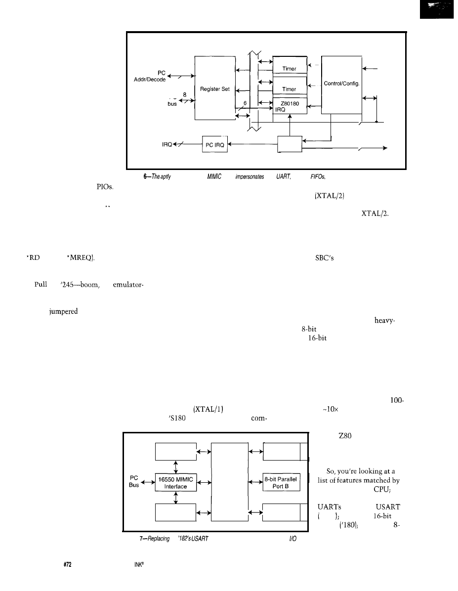
Getting desperate, I pulled
the memory. At this point,
there was little recourse but
to keep pulling chips. If
I
pulled them all, I’d find the
trouble or have plenty of
ammo for calling Zilog.
16550 MIMIC Side
or PC Side Interface
MPU Side Interface
R e c e i v e
Almost as a matter of
formality, I decided to take
one last glance at the sche-
matic before descending to
such a dubiously brute-force
debug tactic.
IS
there any
other chip on the SBC likely
to be butting in?
4
,
280180
Address
16550 MIMIC
Transmit
Register
PC
Data
Control
Data bus
8
,
280180
1
Data bus
P C
DMA
2
Control
280180
Let’s see, there’s the
memory decoder. There’s the
memories. There’s the
There’s the data-bus buffer. There’s
the other data-bus buffer..
DMA Control
Figure
named 16550
logic
a
PC
including
for compatibility with existing
communication software.
Aargh-staring right at me off the
first page of the schematic, and a quick
glance confirms still snugly tucked in
its socket, is another ‘245.
I’m not surprised it’s enabled by the
(not the
Even though
the SBC memories weren’t enabled,
the ‘245 was scrambling the data bus.
the
the
SBC combo works. Plug the ‘245 back
in, but leave the enable pin hanging
out and
to
l
MREQ-it
works. Plug the memories and most of
the other chips in-it works.
I took a quick glance at the offend-
ing code in the monitor source (in-
cluded) to see if
I
could fake it into
working with my preferred terminal
software, but didn’t succeed. Since you
can’t go far without downloading a hex
file, you’re pretty much forced to use
the terminal emulator Zilog provides.
Other potential headscratchers
relate to the fact that the emulator
initialization code doesn’t leave the
CPU in the Reset state. If the programs
you’re testing expect things to start up
a certain way, watch out. I found I had
to use a monitor command to initial-
ize the MMU to the more Reset-like
memory map expected by my program.
patibility
at Reset. Adjust [or
rebuild) the monitor to slow down if
your target only handles
Fortunately, since the target SBC
was already upgraded for full-speed
operation, everything worked grand,
including zero-wait-state execution
out of the
EPROM and proper
operation of the overlay RAM.
NEW CHIPS ON THE BLOCK
Today, Zilog is replaying their ’70s
strategy by combining the ‘180 CPU
with descendants of those old-favorite
peripherals. They have some
duty
chips indeed-contenders
against
chips (including low-end
68ks) and even embedded PCs, espe-
cially for communication applications.
Besides speed, low power, and high
integration, the new chips are ideal for
downsizing (the product, not the job).
Photo 2 traces the ‘180 from its origi-
nal 64-pin shrink-DIP to its latest
pin VQFP, a
space saving.
Consider the Z18 1 in Figure 4-a
modern reflection of the
classic
and peripheral
combo. Remember, the ‘180
core carries its own
I/O forward.
As suspected, installing the SBC
RS-232 transceiver interferes with the
console interface. But now, with every-
thing working, it’s easy to confirm
that the RS-232 interface on the target
can be used just by removing all the
UART jumpers on the emulator.
Similarly, I found a Zilog demo
program that wouldn’t work unless the
monitor set the stack pointer ahead of
time [though the manual says it’s
supposed to be handled automatically).
Having paid my dues the night
before, everything proceeded without
any major problems, just a few small
glitches along the way.
Another potential toe-stubber is
that the emulator initializes itself to
run in turbo
mode while a
real
chip defaults to ‘180
One annoyance is that
the monitor, which other-
wise is completely happy
with any terminal emulator
program, adds an unwel-
come feature for the down-
load hex-file command. It’s
a special protocol that
works in concert with the
included terminal emulator
program, so you can type in
a filename to be down-
loaded.
Baud Rate
Generator
8-bit Parallel
Port A
2180 MPU
COM Decoder
8-bit Parallel
Port c
Figure
fhe
with additional PC interface logic and
makes the Z189 a general-purpose coprocessor.
few other micros:
two
DMA channels (‘180); two
(‘I 80); one
SCC 2-channel,
timers
4-channel,
bit timer/counter with
prescale and external clock
78
Issue
July 1996
Circuit Cellar
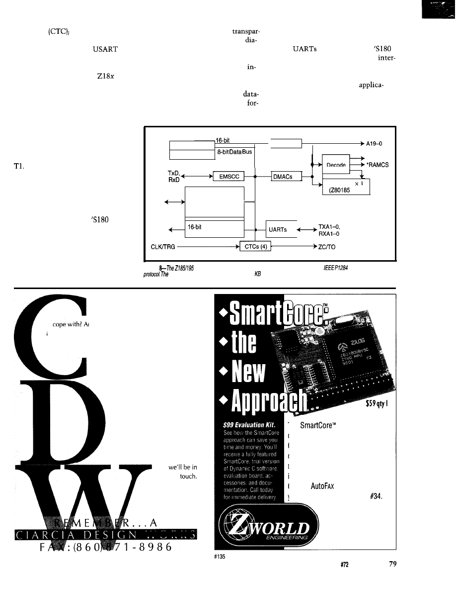
and trigger
and 16 parallel I/O
lines (bit-programmable PIO).
By the way, the “S” in
stands for “synchronous.” Besides
working as a UART (i.e., the “A”), the
SCC in the 2181 and other
chips’
claim to fame is the ability to manage
serial links under a regime know as
HDLC (High-level Data Link Control).
HDLC is rather complicated stuff
that could easily consume an entire
article-I’ll put it on the to-do list.
But, the bottom-line is: HDLC is at the
core of many communications applica-
tions including modems, ISDN, and
One familiar HDLC-based network
is Appletalk (which was, in fact, de-
signed around the SCC).
For higher performance than the
2181, especially for PC communica-
tions applications, the 2182 (see
Figure 5) switches to the
core,
adds a second SCC channel, and boosts
parallel I/O to 24 bits.
Key to easy PC design-in is the
16550 MIMIC logic, which mimics the
16550 UART in PCs, so existing com-
munication software (i.e., anything
looking for COM1-4) works
superfluous-so, it’s removed from the
ently. You see the MIMIC block
‘189. What’s left is an enhanced (with
gram in Figure 6.
faster
and linked DMA)
The 2189 shown in Figure 7 is a
CPU, the MIMIC, some extra PC
variant of the 2182. As the chips
face logic (COM port decoder and
side a modem or fax shrink in number,
DMA interface), and 24 I/O lines.
so a particular function may migrate.
Besides communication
Turns out, the latest modem
tions, I suspect the ‘189 makes an
pumps has taken over the HDLC
excellent data acquisition and control
matting, rendering the ‘182 ESCC
subsytem processor, since high clock
Address Bus
Processor
Power Controller
MMU
l ROMCS
(2)
ROM 32K 8
Parallel Ports (2)
only)
Including IEEE
Bidirectional
Centronics Controller
TOUT
Programmable
Reload Timers (2)
(2)
Figure
are among the first chips to handle the latest and greatest
PC
printer-port
‘185 is a/so
notable for inclusion of 32
of
zero-waif-state ROM.
Does your Big-Company marketing
department come up with more ideas
than the engineering department can
re you a small company that can’t afford
a full-time engineering staff for once-in-a-while designs?
Steve Ciarcia and the Ciarcia Design Works
staff may have the solution. We have a
team of accomplished programmers
and engineers ready to design
products or solve tricky engineering
problems.
Whether you need an on-line
solution for a unique problem,
a product for a startup venture,
or just experienced consulting,
the Ciarcia Design Works is
ready to work with you.
Just fax me your problem and
The
is a shortcut to a
custom-designed controller. It is a
C-programmable microprocessor
core with memory, supervisor,
DMA
,
and clock built in. All you do
is add interface and control logic.
Call our
916-753-0618 from
your
FAX
. Ask for data sheet
1724 Picasso Ave.
Davis, CA 95616
916.757.3737
916.753.5141
FAX
Circuit Cellar INK@
Issue
July 1996
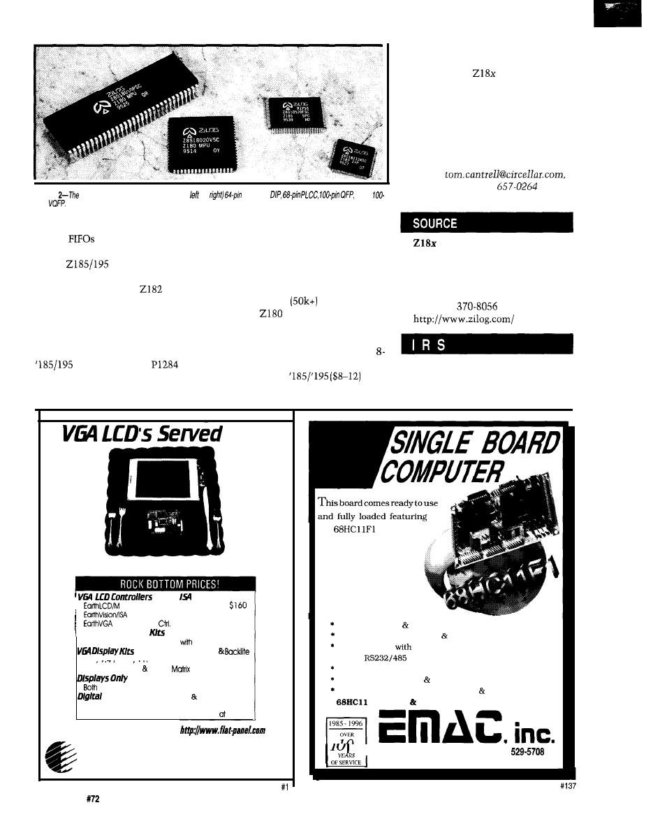
Photo
incredible shrinking ‘180
in (from to
shrink
and
pin
rate,
on-chip DMA controllers, and
MIMIC
(16 bytes each direction)
ensure speedy data transfers.
The
you see in Figure 8 is
another take on the communications
angle. It’s kind of like a
with an
IEEE P1284 (bidirectional Centronics)
port taking the place of the MIMIC.
Conceptually, it makes sense to
consider MIMIC and P1284 as simply
different ways to plug into a PC. The
works as either a
mas-
ter or slave, so it can be used both in a
system and/or peripheral.
Most interesting, the 32 KB of ROM
included on the ‘185 runs with zero
waits for full performance. Still on my
wish list: turn the ROM into EPROM
or flash and add a little RAM. That
would make for one macho MCU.
With volume
prices from $3
to $5, the
(including the regular,
S, and L versions) and the new Z18 1
($7-9) remain formidable competitors
in the midrange and high end of the
bit market. Meanwhile, chips like the
2182, ‘189, and
are
hard to beat for PC plug-in and other
communication applications, espe-
cially those calling for HDLC.
All in all, the
family proves
that chips, like the Phoenix, can rise
from the ashes to soar again.
q
Tom Cantrell has been working on
chip, board, and systems design and
marketing in Silicon Valley for more
than ten years. He may be reached by
E-mail at
by telephone at (510)
or fax
at (510) 657-5441.
Zilog, Inc.
210 E. Hacienda Ave.
Campbell, CA 95008-6600
(408) 370-8000
Fax: (408)
422 Very Useful
423 Moderately Useful
424 Not Useful
Here
for PC
B u s
Monochrome LCD Controller
Color LCD Controller
$280
Analog Input
(VGA to LCD!)
$599
NEW! Touch Screen
Analog resistive touch screen
controller $249
Include LCD. Controller,
7.4” 9.4” 10.4” 11 3”
Starting a-t $220
Mono, Dual Scan Active
in Stock
new and surplus color displays from
$99
LCD Monltors
Desktop LCD ISA Controller
Monochrome Monitors
Starting at $400
Color Monitors
Starting $600
See Earth on the Worldwide Web!
E A R T H
Ph. (714) 448-9368
Fax: (7141448-9316
Computer Technologies
the
processor.
Add a keypad and an
LCD display and you
have a stand alone
controller with analog
and digital I/O. Other
features include:
8 High-Drive Outs 12 Programmable Digital I/O Lines
8 Channels of Fast 8 Bit A/D Optional 4 Channel D/A
Timer/Counters
PWM Capability
* Up to 2
Serial Ports
Backlit Capable LCD Interface
Optional 16 Key Keypad Interface
160K of Memory Space Total, 32K ROM 32K RAM Included
*
Assembler Monitor Included. BASIC Optional
618-529-4525 Fax 457-0110 BBS
P.O. BOX 2042, CARBONDALE, IL 62902
80
Issue
July 1996
Circuit Cellar INK@
The Circuit Cellar BBS
bps
24 hours/7 days a week
(860)
incoming lines
Internet E-mail:
This month,
we start
a
discussion about battery-voltage
defectors. While such a circuit may not sound like a big deal, when
you’re powering if off
you’re measuring, there is more
think about.
Next, I’m
forced overlook long message threads due
space constraints. However, have some extra room this month, so
picked an interesting discussion
by covering how make
high-current connections, and ends talking about conformal coatings.
Talk about thread
Battery loss
Msg#: 3289
From: Ron Turner To: All Users
I need a circuit that detects a battery voltage of 11 V so I
can tell when a car battery drops below this voltage. Does
anyone know of any such circuit?
Msg#: 3304
From: Michael Sharp To: Ron Turner
Look at a simple comparator circuit built around a
741
op-amp. You put a reference voltage on one input pin (the
11 V) and the varying voltage on the other input pin. The
output of the amp goes high or low depending on how you
set it up.
Radio Shack offers Engineer’s Mini-Notebooks wrote by
Forrest Mims III that would explain this circuit (“Op-Amp
IC Circuits” book).
3307
From: Russ Reiss To: Ron Turner
Maxim and Linear Technology sell a number of nice
comparator chips with built-in references that would meet
your needs. Get their databooks and check it out.
Msg#: 3361
From: Ken Simmons To: Ron Turner
How about a simple LM3914 dot/bar driver?
Wire it in dot mode, feed the supply directly into the
input, and when the “11 volt” LED output energizes, have
it drive your alarm trigger. In other words, the V+ supply is
also the signal input and enables the appropriate LED out-
put (sinking drivers!) depending on the level.
I have an old car battery analyzer built around a similar
chip and it works great. Just follow the hookup diagram
that’s on the Radio Shack blister pack for the 3914.
Msg#: 3619
From: Larry G Nelson Sr To: Ron Turner
How about a simple comparitor circuit? Use a voltage
reference to provide a stable reference point and then a
simple resistor divider to sense the battery voltage. As the
battery voltage drops, the divided voltage drops. The voltage
reference (a zener) does not change as the supply voltage
drops and the comparitor can see the difference. If this is in
a car, be aware that the voltage drops drastically when you
run the starter and that could trip the circuit if you do not
have a time delay to filter a short-term drop.
Msg#: 3332
From: George Novacek To: Ron Turner
am assuming you want a circuit which is also operated
from the same battery. What the other gentlemen suggest
(11-V reference) will not work without some modifications.
You can always start with a comparator. You will need a
reference lower than 11 V, such as 5 V-easy to get. The
other comparator input you feed through a suitable voltage
divider. Also, I would use a comparator with an open-collec-
tor output (e.g., LM139 or one of the linear CMOS quads
which have very high-input impedance and a low-current
drain), which is much easier for interfacing with other cir-
cuits.
Another detail to note: you need hysteresis. When you
unload the battery, its voltage is going to creep up. Without
hysteresis, you may see some slow oscillations. What you
want is a setup where the lower hysteresis point is at the
minimum allowable battery voltage, and the high end is
slightly below fully charged battery.
There are several integrated circuits suited specifically
for this purpose (battery chargers/monitors). Or, you can use
a Maxim watchdog IC-most have a built-in voltage moni-
toring circuit. You just add a proper resistor divider.
If you need very low power consumption, get a smoke
detector IC. These are used to monitor a 9-V battery over a
minimum of one year. You end up with just a few
of drain. But, you need a voltage divider since these
circuits trip at 7.7 V.
Circuit Cellar INK@
Issue
July
1996
81
You can also build one from discrete parts, starting with
a zener, a resistor, and a transistor (you can use a
biased base-emitter junction of a transistor for a zener with
only several microamperes knee). With a PUT, I can show
you how to build a battery monitor with no more than 1
drain, should you require it.
term reliability. I’ll try to find Caig’s number unless you
have it handy. Thanks for the input, Ken.
Msg#: 3710
From: Ken Simmons To: Al
Even a 0.092” board may not adequately handle the phys-
ical stresses you’re asking it to.
Bus bar
3511
From: Al
To: All Users
Caig Laboratories, Inc.
16744 West
Dr.
San Diego, CA 92127-1904
(619) 451-1799
Fax: (619) 451-2799
Imagine this. You have a PC board carrying a lot of heavy
AC amps-80 to be exact. The drivers are eight 10-A triacs
connected to different loads. All of the MT1 terminals route
to a large area of tinned copper on the board. You want to be
able to connect to the common of these 10 triacs with a
large-diameter power cable and run it back to the main
breaker box.
Msg#: 3613
From: Pellervo Kaskinen To: Al
Here is what I have done in a similar situation.
I put on the printed circuit board several
wide
For obvious reasons, you don’t want to solder the power
cable right to the PC board. Would you bolt a piece of thick,
fat bus bar to the board? Would you rivet it? How about
soldering it?
disconnect tabs. Then I made a fanned-out cable with quick
connects at the spread out ends and a big ring lug at the
other end. In my case, it was a 50-A application, with six
14-AWG wires. At the common end, there was a crimp-type
ring lug intended for a single
stranded wire. The
stud size was
The bus bar would stub out the end of the board and
have a power terminal on it to capture the power cable.
Which solution would allow for zero ohms at the bus bar to
PC board connection, not oxidize as time goes on, or cause
an IR loss due to dissimilar metal contact?
Now for the kicker. There are four of these nodes spaced
5” apart, and they all must stub out to one power terminal
for connection to the main breaker panel. A total of
320 A....
You could do the same using eight individual wires. You
might want to use a
or stud for the total current re-
quirement. Then you would stack the four ring lugs on a
stud to get the total of 320 A. And, another one or two ring
lugs for a size 0000 (single cable) or 00 (two cables) would be
ready to be stacked in to carry the current away.
3590
From: Ken Simmons To: Al
suggest using a massive bus bar for the main common
and running a piece of fat-gauge
or larger) braid from
the main board to the bus bar. Use some anticorrosion com-
pound (Caig Laboratories makes some interesting ground
plating compounds that might do the trick!) between the
braid/board and braid/bus-bar connections to minimize or
eliminate corrosion and electrolysis effects.
The quick-disconnect tabs are readily available. They
have two legs that you have to solder to the PCB. A general
problem is the solderability. Our tabs always are old by the
time we try to solder them and that does not help. You may
need to pretin them or use some rather active flux. A
double-sided board with plated-through holes may be easier
than my single-sided board, but I would still advise you to
check for the optimum hole size.
Msg#: 3629
From: Al
To: Pellervo Kaskinen
Using braid interfacing rather than a physical bus-bar
mounting greatly reduces the mechanical stress on the
main board.
have seen 0.250”-wide quick disconnects and use them
in some of my other products, but have never seen ones the
size and current capability that you are describing. Where
would I get more info on these monsters?
3883
3593
From: Pellervo Kaskinen To: Al
From: Al
To: Ken Simmons
The board will be 0.092” thick to handle mechanical
stress along with strategically placed standoffs. This paste
that you mentioned sounds like the thing I need for
You
have seen them, you just have not realized their
potential! The 0.250” quick connects are rated 10-A de-
pending on the other side of the pair and the wire size. I
hope I did not lead you to believe they would be good for
82
Issue
July
1996
Circuit Cellar INK@
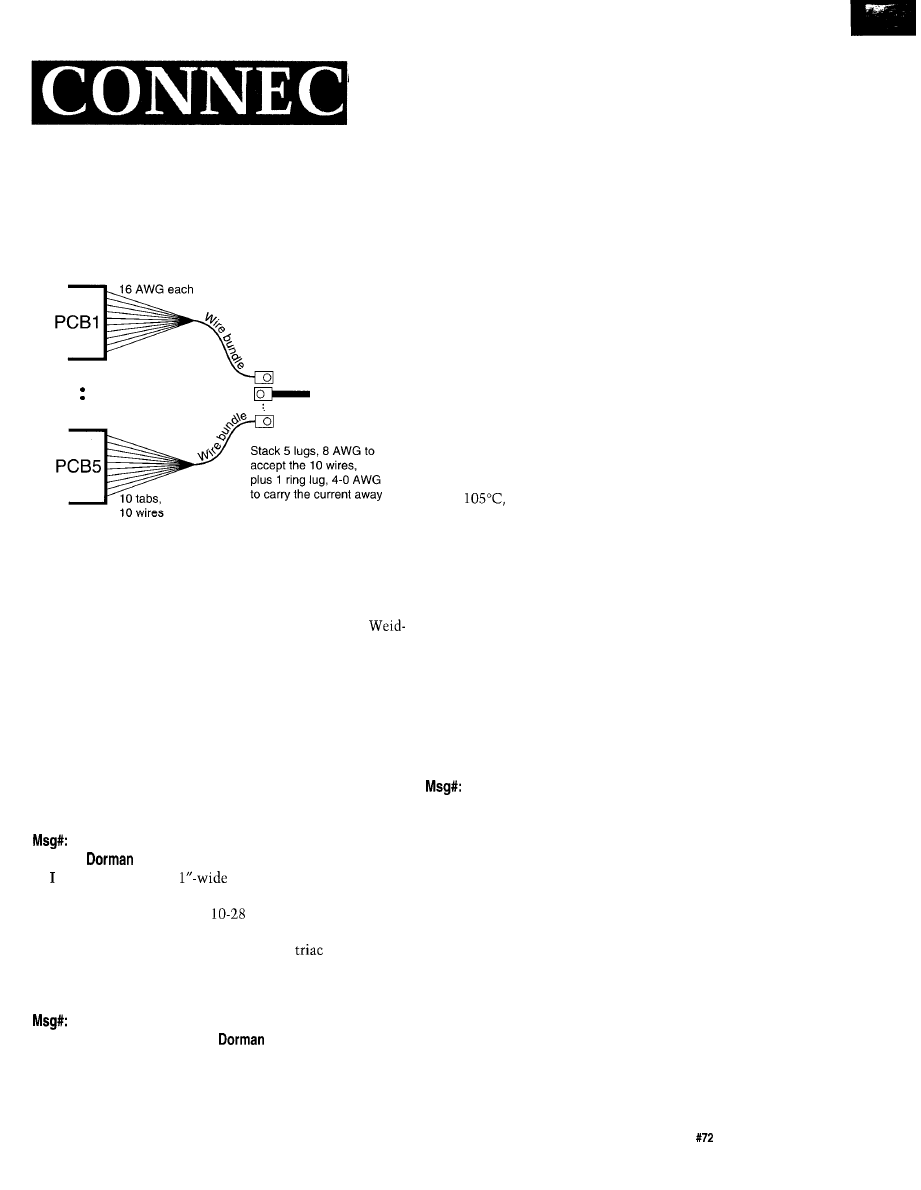
TIME
the 80-A portion. That has to be handled by the ring lugs on
a stud.
Let’s see if I can clarify the idea with some graphics.
10
tabs,
10 wires,
5 boards in all
.
4-O AWG
The stud, of course, has to be mounted somewhere.
There are commercial products that may be useful. They
consist of an insulating block and a well-anchored stud.
Available at least from Marathon, USD, Phoenix, and
muller. Sorry, I did not check the addresses for these com-
panies, or if the first two even exist (under the same name).
Weidmuller and Phoenix both exist-I have done business
with them quite recently.
One more source I know of is a cabinet maker, Rittal.
But of course, you can make your own from 1” fabric-rein-
forced phenolic block, an ordinary bolt, and some epoxy to
lock the bolt head inside the bottom-side counterbore. The
epoxy also keeps the bolt head from making a short to any
metallic mounting surface.
3692
From: Al
To: Pellervo Kaskinen
decided to opt for a
copper bus bar strapped
across the boards. This way there is not so much labor in-
volved. The bus bar has two
studs for common AC
connection. I wasn’t aware that a 0.25” terminal would hold
so much current. Of course, the FAS-PAK
series used
0.25” slip-on-type connections, and they say you can get
30 A through it with a Molex slip-on female plug.
4147
From: Pellervo Kaskinen To: Al
If the flat tab sits on a heat sink, of course you can get
more current capacity. But the normal ratings and what the
agencies (UL and others) approve is in the 10-16-A range.
If you look at some circuit breakers or fuse holders, you
find somewhere a statement that the flat terminals cannot
be used for a current beyond 16 A or so, unless you solder
the wire on the tab. In other words, they know that exces-
sive heat causes a problem for ordinary quick-connect com-
binations.
I think the problem is assumed to be mostly related to
thermal cycling, heat-cool-heat-cool, and so on. But, I do
not have any actual data about that.
On the other hand, the semiconductor connections,
especially the cables of stud-mount-type SCR packages,
have always been very flimsy in comparison to the normal
cables. That is partly due to the fact that the semiconduc-
tors are typically operated at a derated current. Another
reason for that is the higher temperature specification.
While a typical cable is insulated with a PVC jacket, the
SCR connection cables are either uninsulated or have a
silicon rubber jacket. The temperature rating for the PVC is
about
while the silicon rubber can be up to 180°C.
Not to forget that the SCR bridges are almost always well
cooled with a powerful fan.
Anyway, I am against generalizing the 30-A rating your
FAS-PAK suggests.
Msg#: 4216
From: Ed Nisley To: Pellervo Kaskinen
Speaking of high current, there’s the issue of soldering
ground wires. Turns out that a decent lightning stroke sim-
ply vaporizes the solder (it’s a poor conductor) and leaves
you with two disconnected conductors. Welding, yes, bolted
connectors, yes, solder, nope.
That’s not an issue with ordinary electrical components,
but I can’t resist tossing it into the discussion.
5099
From: Pellervo Kaskinen To: Ed Nisley
Good point! Yet, I just cannot bite that without a little
qualifier.
The age-old rule about soldering electrical conductors is
that the solder is there only to seal the connection, not to
make it. I recall some quite big campaigns that one TV
manufacturer ran to convince prospective customers that
their TVs were made to be reliable-like most of the prob-
lems in “conventional” (what else?) units were due to fail-
ing soldered connections. They, on the other hand, never
trusted the solder alone. No sir! They made each connec-
tion between the component leads inside a cone of wrapped
copper wire, similar to a wire nut. But then, they filled the
cone with solder.
The solder, applied that way, was supposed to immobi-
lize the leads plus protect the actual contact points against
oxide formation and other dirt attacks.
Circuit Cellar INK@
Issue
July 1996
8 3
If you have ever built any
items, chances are
you got a good education about the component mounting
and soldering within rows of eyelets or other mounting
ears. Push the lead in the hole, bend it, don’t solder yet!
Add other components the same way, locking the compo-
nent lead tightly in place so it actually works, even without
the solder. Then, finally apply the heat and a little later the
solder.
Ahh! Those were the days.. Then came printed-circuit
boards. You just could not compete with the manufacturing
efficiencies, no matter how reliable the solder-cup method
was. A single-sided board, a double-sided board. Multilayer
boards and surface mounting. Where have we gone with the
idea of having the solder as only a seal? Nowadays, solder is
actually part of the conductive path.
Regarding the use of flat tabs on printed circuit boards in
high-current applications, here is one personal finding to
conclude my reminiscences. Ordinarily, the holes on the
printed-circuit board should be made large enough to leave
about 0.006” space on all sides of the component lead. That
makes the wetting action best. You also can desolder such
connections much easier, if necessary.
But, the tabs are next to impossible to keep straight and
in place during the soldering operation if the holes are any
larger than barely large enough. I make the holes barely
large enough to accept the two legs of the tab. A certain
amount of force is required to force the legs in the holes. So,
in practical terms, I’m back to the “electrical contact with-
out solder” principle. The solder is again applied mostly for
the purpose of locking the part in place and protecting the
connection.
5187
From: Ed Nisley To: Pellervo Kaskinen
You
mean, gasp, that “The Bigger The Blob, The Better
The Job” isn’t the right rule?
Me, I’ve always been a fan of structural solder..
(Grin!)
7198
From: Ken Simmons To: Ed Nisley
You got it!
I was once mil-spec solder certified and if you compare
the amount of solder allowed on mil-spec hardware versus
good-quality commercial/industrial hardware, the commer-
cial/industrial stuff looks like garbage in relation to the
amount of solder on the pads, etc.
In other words, mil-spec makes everything else look like
your structural solder definition.
If you want something even tighter, NASA solder
makes mil-spec soldering look like structural solder by
comparison!
84
issue July
1996
Circuit Cellar INK@
4923
From: Al
To: Pellervo Kaskinen
They go on to say that to get 40 A out of a 40-A
(FAS-PAK), you have to solder a 4-AWG wire directly to the
terminal. I think AMP is exaggerating when they say you
can get 30 A from a 0.250” slip-on.
7617
From: Pellervo Kaskinen To: Al
I have not checked the particulars, but my gut feeling is
that AMP is actually playing on the weaknesses of the
cheap competition.
I have myself been unhappy about some flat-tab connec-
tors made of too-thin metal. They just folded it more for
increased stiffness. Might be fine for 20-AWG wires, but not
for the thick 12 (or even 10) AWG. And I know there have
been changes during the years in the color codes indicating
wire size. Nowadays, I have to use a blue one for some sizes
that originally went with the red. Maybe UL or somebody
else pointed a few things out to the vendors?
On the other hand, with proper tooling, optimum condi-
tions, and fixed room temperature, you might get ultimate
temperatures within acceptable values even at 30 A per tab.
Just do not take it as a relevant number for any brand, any
contact density, and any ambient temperature. In fact, the
neighboring contacts put out heat, which affects the ambi-
ent temperature. You always need a derating table to find
what the realistic values might be.
This reminds me of a difference in fuse-holder ratings
between the European and the American specifications. The
American tests are conducted with a fuse-size solid-copper
bar in place of the fuse. This naturally causes less heat gen-
eration than a real fuse would do, so the holder gets rated
for higher current than what the maximum fuse size should
be. An American lo-fuse holder may earn a 6.3-A rating in
Europe because it is tested with such a fuse in place.
But, the street is sometimes in the opposite direction.
Lately, the European cable-size recommendations have
started using the UL principles of determining an individual
rating and a conduit- or raceway-dependent derating table.
The old way assumed “typical” conditions, with increased
ambient temperature to be the norm.
You do use the derating table, don’t you!
Actually, all I see most of the time is people learning the
basic table values: 14 AWG is good for this much current,
period. Using the two derating factors given by the NES can
easily cut more than one third of the capacity!
13004
From: Al
To: Pellervo Kaskinen
What I have learned, as a rule of thumb, about derating
for high-current consumption is to multiply by two. If the
circuit calls for a 20-A load, I use a 40-A
If a 10-A fuse
is required, I select a 25-A clip to hold it.
After seeing boards burn up due to overheated connec-
tions,
I
assume that oxidization and time are a power con-
nection’s worst enemy. If the board is to be used in a harsh
environment such as a sign or other locale, this factor mul-
tiplies. I use a dry-can desiccant to reduce moisture.
However, all math aside, second guessing Gea involves a
more blunt approach. Two times works for me.
From: Pellervo Kaskinen To: Al
The factor of two is a little more than the NAVMAT (I
think that is what it is called)
wants you to do. They
have based the derating on the power, not the current or
voltage. The square law dependency means the current and
voltage are derated by a factor of 0.7, while the power be-
comes derated by a factor of 0.5.
From: Ken Simmons To: Al
Don’t forget conformal coating as a good option for
weatherproofing your board. Urethane-based coatings (like
Hysol PC-
are excellent moisture barriers and quite
electrically inert. Even silicone RTV coatings, while thicker
and a little more expensive, are excellent for real harsh
environments.
One disadvantage of conformal coating is high rework
cost. It’s difficult at times to remove the cured coating (es-
pecially silicones!) and you have to
the reworked area
and let it cure before restoring the device to service.
However, the advantages far outweigh any disadvantages
as far as I’m concerned.
From: Pellervo Kaskinen To: Ken Simmons
once was in a seminar where a high-precision-resistor
manufacturer described these environment problems and
some solutions. The one shocking piece of info was that
silicone coating did not work well!
The reason was that silicone did not adhere intimately
enough to the component surface to prevent seepage of
water. Rapid temperature changes caused the water to ex-
pand and further rip open the channel along the component
surface. Then cooling sucked more water in and the next
heating..
Their solution was a dual barrier. Epoxy that is too hard
for the overcoat was good for the inner layer. Very low vis-
cosity to produce a thin layer. Then silicone for mechanical
reasons.
From: Ken Simmons To: Pellervo Kaskinen
Fascinating! Perhaps you should send a dissertation to
the
and other aerospace electronics manufacturers
informing them of this fact.
In my experience with environmental stress screening
using silicone-encapsulated
we’ve never had any
problems with water seepage, infiltration, and so on. Of
course, our boards are precoated with primer compound
before the actual silicone is applied.
I would think the epoxy would be good for the mechani-
cal securing, not the silicone.
Of course, there are so many formulations of silicone
this statement can be both right and wrong at
the same time, no?
From: Al
To: Ken Simmons
I,
too, was an advocate of conformal coatings, however
over the years and after plenty of rework difficulties, I have
changed my views on the advantages of conformal coatings.
A weathertight container and a 2” x 3” wafer of desiccant
appears to work just as well. Placing the can on or near a
radiating
drys out the can and allows for continu-
ous use.
From: Ken Simmons To: Al
True, however such an option is not acceptable with
military flight hardware that’s enclosed in perforated enclo-
sures.
Remember, these things are designed to literally be in-
stalled and forgotten, enduring the environment until a
failure occurs.
Yes, conformal coatings add a little to the cost, as well as
some rework difficulties, but they can’t be beat for moisture
protection as well as possible short-circuit protection from
those unexpected things that invariably end-up making
their way into the product (e.g., dust, insects, etc.).
From: George Novacek To: Al
Depends on the environment. For some applications, you
can’t do without conformal coating. If your box is exposed
to significant temperature and barometric pressure varia-
tions (e.g., on board an aircraft), you must provide a breath-
ing hole in the enclosure
is all you need) to allow the
air pressure equalization and to drain the condensation.
A hermetically sealed box is extremely expensive and
difficult to build. Even with gaskets and seals, the box
breathes a little (e.g., temperature expansion and contrac-
tion, connectors, etc.). There is eventually enough moisture
Circuit Cellar INK@
Issue
July
1996
8.5
trapped inside the box to cause problems. (This is not theo-
Don’t believe I’ve heard of Parylene. Can you elaborate
retical! It has been shown to happen.)
on what it is!
Making the box hermetically sealed and expandable so
that it can equalize pressure by adjusting its volume is not
only expensive, but you run into numerous problems with
shock and vibration. And still, there are the connectors to
worry about.
Modern conformal coating materials allow easy applica-
tion and full UV curing in about
10
seconds.
From: Pellervo Kaskinen To: Ken Simmons
Parylene is a trade name for coatings that are applied in a
vacuum chamber. I once responded to some ad with the
appropriate bingo card mark. Received several pages of nice
PR with an impressive list of customer names. And too
little hard facts, as usual. Moreover, I don’t know where I
have “safely” filed it.
From: Pellervo Kaskinen To: Ken Simmons
Maybe I didn’t make it as clear as I thought. The idea
about the epoxy/silicone double coating was not mine. In
fact, it came from one of the foremost suppliers of
precision resistors. I have no doubt whatsoever that they are
suppliers for NASA and the rest of the aerospace industry.
However, I may emphasize the key points a little more.
The epoxy coating was deemed to be too hard and brittle to
survive the mechanical challenges. Something softer, like
the silicone was needed for good impact resistance. A com-
bination with silicone inside would not offer any benefits,
while the silicone on top does.
In any case, I have never used that service and the only
exposure that I have had to parts coated with Parylene have
been some ferrite toroids. When you see other color than
dark gray on a ferrite, it might be coated with Parylene.
If I understood, the vacuum process makes the coating
extend to all places, leaving no “shadows.” Also, you do not
get the ridges a dip and dry process leaves. And, with the
thin coating you can maintain close tolerances.
Now, this also was not a board coating. It was for indi-
vidual resistors. The data that was shown covered salt
spray, thermal cycling, and just about all the torture tests
the MIL system knows of. It indicated an order-of-magni-
tude improvement over either an epoxy-only or a
only coating performance.
We invite you to call the Circuit Cellar BBS and exchange
messages and files with other Circuit Cellar readers. It is
available 24 hours a day and may be reached at (860) 871-
1988. Set your modem for 8 data bits, 1 stop bit, no parity,
and 300,
9600, or
bps.
All of that was before Parylene, so maybe it is not valid
anymore. Cannot keep truly up-to-date on these issues. The
bean counters don’t like expensive seminars..
From: Ken Simmons To: Pellervo Kaskinen
The silicones we use in the
side of Boeing have
very high moisture resistance, provided they’re applied
correctly (i.e., clean surfaces, well-primed). In fact, I’ve yet
to see one of our boards returned for a moisture-related
failure. They’re usually electrical or mechanical failures.
Software for the articles in this and past issues of
Circuit Cellar INK
may be downloaded from the
Circuit Cellar BBS free of charge. It is also available on
the Internet at
For those
with just E-mail access, send a message to info@
circellar.com
to find out how to request files through
E-mail.
Now when you talk about individual components, you’re
dealing with a different area than a completed PWA. Our
tests aren’t used to qualify vendor components (resistors,
caps, etc.), only the completed end-item
That’s
where we apply the final silicone (or urethane) conformal
overcoat. The individual components are basically on their
own in surviving our tests.
Of course, our supply documents only list vendors whose
components have been previously determined to meet the
required design specs (temperature, shock, humidity, etc.).
Thus, it’s our PWA assemblies that require the final envi-
ronmental qualification testing.
For those unable to download files, the software is
also available on disk. Software for issues prior to 1995
comes on a 360-KB IBM PC-format disk, one issue per
disk. For issues from 1995 on, software comes on a
PC-format disk, with three issues per disk.
Disks cost just $12 each. To order Software on Disk,
send check or money order to: Circuit Cellar INK,
Software On Disk, P.O. Box 772, Vernon, CT 06066, or
use your Visa or Mastercard and call (860) 8752199.
Be sure to specify the issue numbers with your order.
Please add $3 for shipping outside the U.S.
425
Very Useful
426 Moderately Useful
427 Not Useful
86
Issue
July
1996
Circuit Cellar INK@
wo of the concepts remember most about working in a couple of large aerospace companies were the
ideas of “designing by committee” and “debugging by default.”
First, you take a bunch of engineers and managers and sequester them in a conference room. Lunch, dinner,
snacks-whatever-are brought in for however many days are required for management to hammer engineering into submission.
Vacations are canceled, sick leave is scorned, bathroom trips are supervised.
After a couple weeks of this routine, and depending on the deviousness of management, the engineering staff has not only
become enlightened to the prospects of creating cold fusion and perpetual motion, they’ve taken full responsibility for creating
whatever management thought up. Of course, the engineering staff gets to determine which poor souls actually do the job.
At the bottom of the “to do” list-the last task to be considered-is making it all work
debugging it). In my large-company
experience, this is when everyone heads for the hills. The unfortunate guys without trips, meetings, conventions, or other “important
business stuff” get scope-probe duty. Invariably, the newly hired engineers are in this group. Needless to say, they can forget free
time and vacations for the next six months.
I’m sure I’m not telling you anything new. If you work for a small company now, your past experience includes a stretch as a
disposable debugger. By now, you’re positioned to delegate the task to others. If you’re still in a large company, you probably have
enough experience to come up with some really “important business stuff” and avoid the problem entirely.
For the rest of us-and in this lot I’m including those without the power to delegate as well as masochists like myself who feel
that holding a scope probe now and then keeps us closer to the pulse of the business-the debugging process can be either a
challenge or a sentence.
Somewhere at the bottom of the heap are these people and tools that make products sensible and designs a reality. Like
running a marathon, you need the most commitment and the most effort when you’re heading to the finish line. Since human nature,
unfortunate as it is, only rewards the winner, you’ve got to get there.
Even with all the implied responsibilities, I’d like to think we save the best experiences for last. The unsung heroes who actually
make the committee design functional achieve this goal through hard sweat and tenacious resolve. In the process, they learn the
most important lesson: how to do or not do things next time.
Product debugging isn’t a static encounter. Good engineers take the experience and try to reduce the debugging required on
their next effort. The others find out that debugging often takes more talent than they have. For them, just being part of the committee
or doing other “important business stuff” is safer and less demanding.
96
Issue July 1996
Circuit Cellar
Wyszukiwarka
Podobne podstrony:
circuit cellar2001 07
circuit cellar2000 07
circuit cellar1995 07
circuit cellar2002 07
circuit cellar1993 07
circuit cellar1994 07
circuit cellar1997 07
circuit cellar2004 07
circuit cellar1994 07
circuit cellar2004 07
circuit cellar1996 07
circuit cellar1995 07
circuit cellar1997 07
circuit cellar1993 07
więcej podobnych podstron