Unfulfilled Anticipation
0
here you sit, hungry, frustrated, mouth watering.
You’ve been thinking about it all day. The last time
you were at the local mall’s food court, you tasted a free
sample of their special sandwich. Now you’re back for a more
substantive meal, and all you find is “Closed. Out of Business.” Sure there
are other vendors around, but you’d been really looking forward to this
shop’s treats.
What does this sad story have to do with Circuit Cellar
Well, I’m
sorry to report that after last month’s introduction to a
on
machine vision (“Machine Vision: Industrial Inspection,”
we had to
cancel the series. It came down after last month’s issue had gone to press,
and it was completely out of our hands and those of the author.
In its place, veteran Jan Axelson graciously agreed to fill in with a pair
of articles on using serial
She starts this month with a descrip-
tion of the most common serial interfaces (SPI, Microwire, and
and
concludes next month with a sample application.
I’m getting ahead of myself, though. Kicking off this month’s features,
we have an article from a favorite author, David Prutchi, on generating
frequency waveforms using digital techniques. It’s not just a simple matter of
sticking in a small processor.
Next, William Hohl and Joe Circello light up
with some
algorithms for doing orthogonal manipulations. Finally, David Tweed finishes
up his Canadian
receiver project.
In our columns, I’ve already mentioned Jan Axelson’s EEPROM lead-in
article. Following Jan, Jeff teaches his robot to speak. And, Tom rifles
around the parts drawer and comes out with a handful of new chips that do
specific tasks very well.
begins with Chip Freitag describing how to add an Ethernet
interface to embedded controllers. With the Internet growing like wildfire, it’s
only a matter of time before you have an Ethernet backbone in your house
with everything connected to it.
Next, David Feldman gives you some pointers for submitting a winning
entry to
Embedded PC Design Contest. In
Quarter, Mike
Justice and Phil Marshall survey
interfaces for
Finally, Fred
Eady continues the Internet-connected embedded controller concept by
assembling the smallest Web server you’ve likely ever seen.
2
Issue 94 July 1997
Circuit Cellar
INK@
T H E C O M P U T E R A P P L I C A T I O N S J O U R N A L
EDITORIAL DIRECTOR/PUBLISHER
Steve Ciarcia
EDITOR-IN-CHIEF
Ken Davidson
MANAGING EDITOR
Janice Hughes
TECHNICAL EDITOR
Elizabeth
ENGINEERING STAFF
Jeff Bachiochi
WEST COAST EDITOR
Tom Cantrell
ASSOCIATE PUBLISHER
Sue Hodge
CIRCULATION MANAGER
Rose
CIRCULATION CONSULTANT
John Treworgy
BUSINESS MANAGER
Jeannette Walters
ADVERTISING COORDINATOR
Dan Gorsky
CONTRIBUTING EDITORS
Rick Lehrbaum
Fred Eady
NEW PRODUCTS EDITOR
Weiner
ART DIRECTOR
KC Zienka
CIRCUITCELLAR
THE COMPUTER
JOURNAL (ISSN 0696-6965) is published
monthly by Circuit Cellar Incorporated 4 Park Street,
Suite 20, Vernon,
(660)
Periodical
rates
paid at Vernon, CT and
offices.
year (12 issues) subscription rate U.S.A. and posses-
sions $21.95,
$31.95, all
PRODUCTION STAFF
John Gorsky
James Soussounis
tries $49.95. All subscription orders payable in U.S.
funds only, via
postal money order or
checkdrawn on U.S. bank.
Direct subscription orders and subscription related
questions to
Cellar INK
P.O.
POSTMASTER: Please send address changes to
Holmes,
PA 19043.9613.
Cover photograph Dianne Barry
PRINTED IN THE UNITED STATES
For information on authorized reprints of articles,
contact Jeannette Walters (860) 875-2199.
ASSOCIATES NATIONAL ADVERTISING REPRESENTATIVES
NORTHEAST
MIDWEST&SOUTHEAST
WEST COAST
MID-ATLANTIC
Collins
Barbara Jones
Barbara (Best)
(954) 966-3939
Shelley
(561)
Fax: (954) 965-6457
(714)
Fax: (561)
Fax: (714)
Cellar BBS-24
bps, 6 bits, no parity slop bit, (660)
For information,
World Wide Web:
All programs and schematics in Circuit Cellar
have been carefully reviewed to
their
is
inaccordance
the specificationsdescribed,
transfer by subscribers.
programs or schematics
consequences of any such errors.
of possible
in the quality and condition of materials and workmanship of reader-assembled
Circuit Cellar
disclaims any
for the safe and proper function of reader-assembled projects
upon or from
plans, descriptions, or information published in Circuit
Entire contents copyright 1997 by Circuit Cellar Incorporated. All rights reserved Circuit Cellar
a
registered trademark of Circuit Cellar Inc. Reproduction of this publication in whole or in
without
consent from
Cellar Inc. is prohibited.
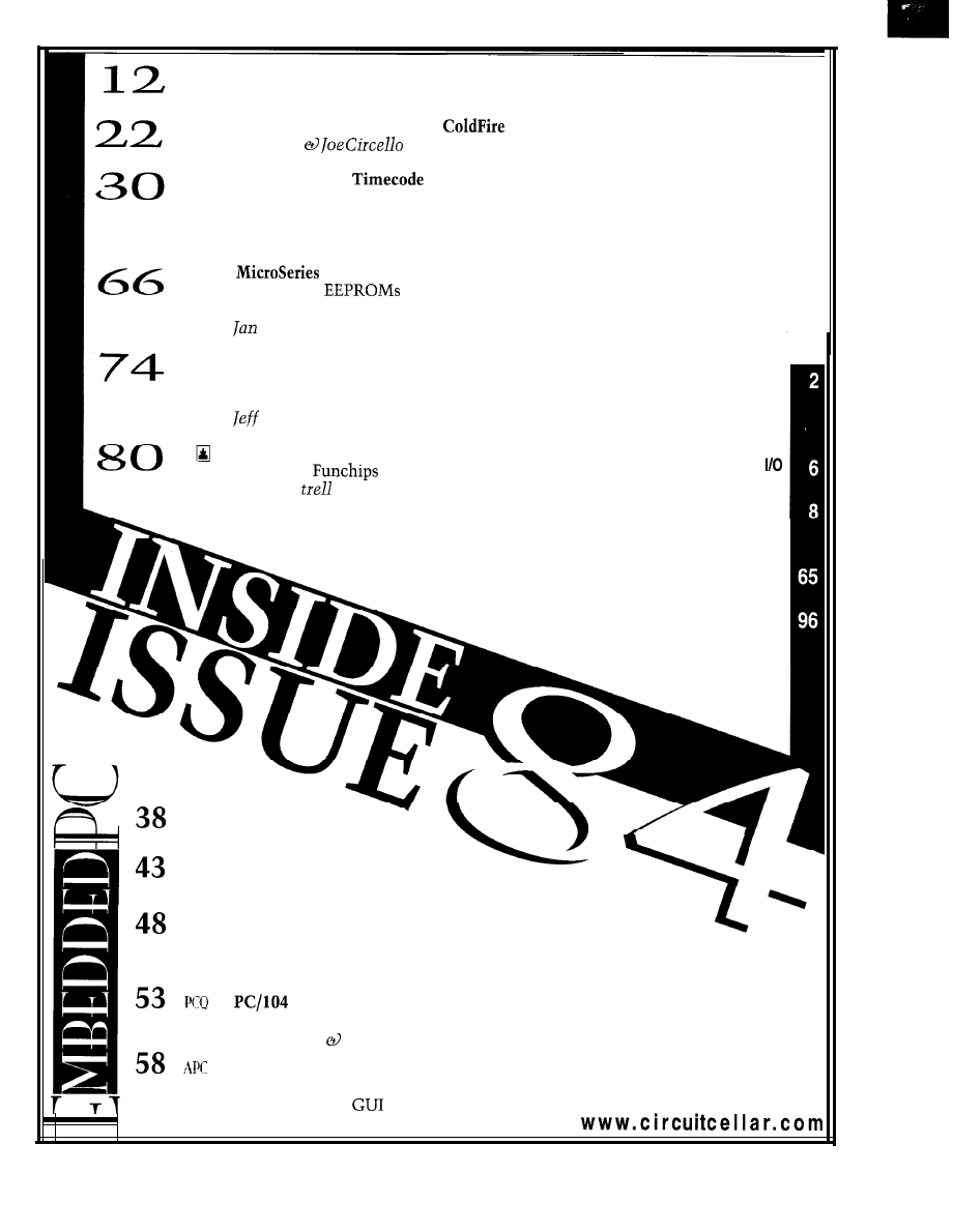
Digital Generation of High-Frequency Waveforms
David Prutchi
Frequency Domain Analysis with
William Hohl
DSP-Based Canadian
Receiver
Part 2: Application Considerations
David Tweed
q
Using Serial
Part 1: General Principles
Axelson
q
From the Bench
It Can’t Be A Robot
Task Manager
Part 2: It Doesn’t Talk
Ken Davidson
Bachiochi
Unfulfilled Anticipation
Silicon Update
Cruise the
Reader
Tom Can
New Product News
edited by Harv Weiner
Advertiser’s Index
Priority Interrupt
Steve Ciarcia
Don’t Lose Your Head
Nouveau PC
edited by Harv Weiner
A Stand-Alone Embedded Ethernet Platform
Chip Freitag
A Formula For Winning
Product-Development Strategies
David Feldman
Quarter
Industrial I/O Networks
Mike Justice Phil Marshall
Applied PCs
Internet Appliance Development
Part 1: From the
Up
Fred Eady
Circuit Cellar INK@
Issue 84 July 1997
3
CONTESTS AND INTELLECTUAL PROPERTY
As I looked at the rules for entering INK’s Embedded
PC Design Contest, I was concerned by this rule:
“All contest entry materials..
the property of
Circuit Cellar INK
and will not be returned under normal
circumstances. All contestants entering projects in the
Embedded PC Design Contest agree to assign Circuit
Cellar INK
exclusive first-publication..
The winners will receive monetary prizes:
First Prize $5000
Second Prize $3000
Third Prize $2000
Three Honorable Mentions $250 (each)”
I fear that you and your sponsors are using $10,750 to
“steal” other people’s work and ideas.
TF
First, let me explain that “entry materials” refers
only to the paperwork sent in by entrants. You can imag-
ine the logistical nightmare of tracking and returning
every bit of paper to its rightful owner. We’re simply
making sure that we spend our energy making a good
magazine, not just shuffling paper.
Secondly, as with all
INK design contests, the intel-
lectual property of all submitted designs remains with
the contestants. Rest assured, we won’t forward your
entry to the sponsoring companies. As well, the judges
are bound by a nondisclosure agreement. They cannot
use any submitted design to further their own business
enterprises.
This is our ninth design contest, and we have
and will never-use any submission to manufacture a
product. Remember, our interest is in bringing you a
high-quality engineering journal. We won’t jeopardize
our relationship with you by “stealing” your designs.
Editor
RIGHT ON THE MONEY
Steve, thanks very much for your opinion (“When It
Costs Nothing, What’s It Worth?” INK
I especially
enjoyed it when you asked, “What real value is there in
rushing to upgrade to the latest..
when your
actual throughput is [less]?”
Bang on. Give the man a cigar!
William F.
ARM TIED BEHIND BACK
Randy Heisch’s “A PowerPC
Embedded
Controller Prototype” and Art Sobel’s “Embedding the
ARM7500” (INK 82) made for good reading. Art’s state-
ment that the ARM7500 is almost an entire PC in a chip
may be true, but I think that Motorola has a better solu-
tion with their MPC821 CPU.
The MPC821 has a PowerPC as the core with a RISC
CPU to handle all I/O. The I/O includes two high-speed
serial ports-one set up as an Ethernet
port, and the
other as an SDLC port. Alternative uses for these
high-speed serial ports would be ISDN channels.
An LCD controller is included along with an IR inter-
face, dual-port PCMCIA controller,
bus controller,
single-wire serial bus, parallel port, and speaker port. The
MPC860 drops the LCD controller in favor of two more
normal-speed serial ports. DMA and a memory controller
are also included with all
devices. All this is
contained in approximately a
1
ball-grid array pack-
age. All
devices also support JTAG and basic
debug ports, so an in-circuit emulator isn’t required.
The ARM may have a future, but I think the PowerPC
will capture a larger market share-especially in the VME
market, where it will overtake the 68k. As for embedded
applications, the
family is an excellent choice.
Dan Farkas
Contacting Circuit Cellar
We at Circuit Cellar
communication between
our readers and staff, so we have made every
to make
contacting us easy. We prefer electronic communications, but
feel free to use any of the following:
Mail: Letters to the Editor may be sent to: Editor, Circuit Cellar INK,
4 Park St., Vernon, CT 06066.
Phone: Direct all subscription inquiries to (800) 269-6301.
Contact our editorial offices at (860) 875-2199.
Fax: All faxes may be sent to (860) 871-0411.
BBS: Editors and regular authors are available to answer ques-
tions on the Circuit Cellar BBS. Call (860) 871-l 988 with
your modem
bps,
Internet: Letters to the editor may be sent to
corn. Send new subscription orders, renewals, and ad-
dress changes to
Include
your complete mailing and E-mail addresses in all corre-
spondence. Author E-mail addresses (when available) may
be found at the end of each article. For more information,
send E-mail to
WWW: Point your browser to
6
Issue
84 July 1997
Circuit Cellar INK@
Edited by Harv Weiner
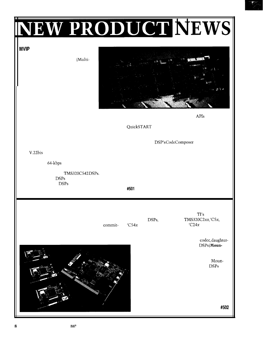
DSP RESOURCE BOARD
DSP Research has announced the
VIPER-12,
a
high-density MVIP
vendor Integration Protocol) DSP resource
board for computer telephony and tele-
communications infrastructure applica-
tions. The board is an ideal platform for
wireless and cellular base stations, re-
mote access servers, voice/modem/fax
over ATM/frame relay, and satellite base
stations.
Each VIPER- 12 services up to 24 IS- 136
digital cellular vocoders including line
echo cancellation, keeping the per-channel hardware
cost under $200. For voice-over-network applications,
the board can translate, or transcode, between different
voice-compression standards. It also services multiple
channels of fax/modem connections-a useful feature in
Internet remote access, fax-back, and pager servers. The
VIPER-12 supports up to 12 simultaneous V.34, 24 fax,
or 48
connections per board. As an open DSP
resource board, its MVIP bus interface gives access to
256 full-duplex
channels.
The VIPER- 12 combines the MVIP bus with the power
of 12 Texas Instruments
At 40 MIPS
of performance, the
allow multiple channel or port
assignments. With 12
per board, the VIPER-12 has
an extremely high channel density.
The VIPER-12 is supplied with host
for the MVIP
switch control and DSP-host communications, plus the
DSP operating environment. The full
complement of development tools includes the TI C
compiler with assembler and linker, a DSP program
loader, and GO
Debugger.
Single-board pricing for the VIPER-12 starts at $4995.
DSP Research
1095 E. Duane Ave., Ste. 203
Sunnyvale, CA 94086
(408) 773-l 042
l
Fax: (408) 736-3451
www.dspr.com
DSP UNIVERSAL EVALUATION MODULE
The Mountain-Uevm enables engineers to evaluate
different fixed-point Texas Instruments DSP chips for
various applications without the cost and time
ment of traditional prototyping. Interchangeable DSP
modules (daughter cards) facilitate chip selection.
The Mountain-Uevm supports all of
popular
fixed-point
including the
and
families, as well as the new
motor-control
family. The half-size PC/AT plug-in card features an
FCC-approved telephone Data Access Arrangement
(DAA), 16-bit stereo audio interface
card site to accommodate different
tain-Paks),
and debug using both on- and off-card
emulation.
The Mountain-Uevm is priced at $995.
tain-Pak modules for various fixed-point
cost
$495 each, including debugger software. Optional TI
C/assembly source debugger and debugging environ-
ments from GO DSP are available.
White Mountain DSP
20 Cotton Rd.
Nashua, NH 03063
(603) 883-2430
l
Fax: (603) 882-2655
Issue
84
July
1997
Circuit Cellar
LOW-COST DSP CHIP
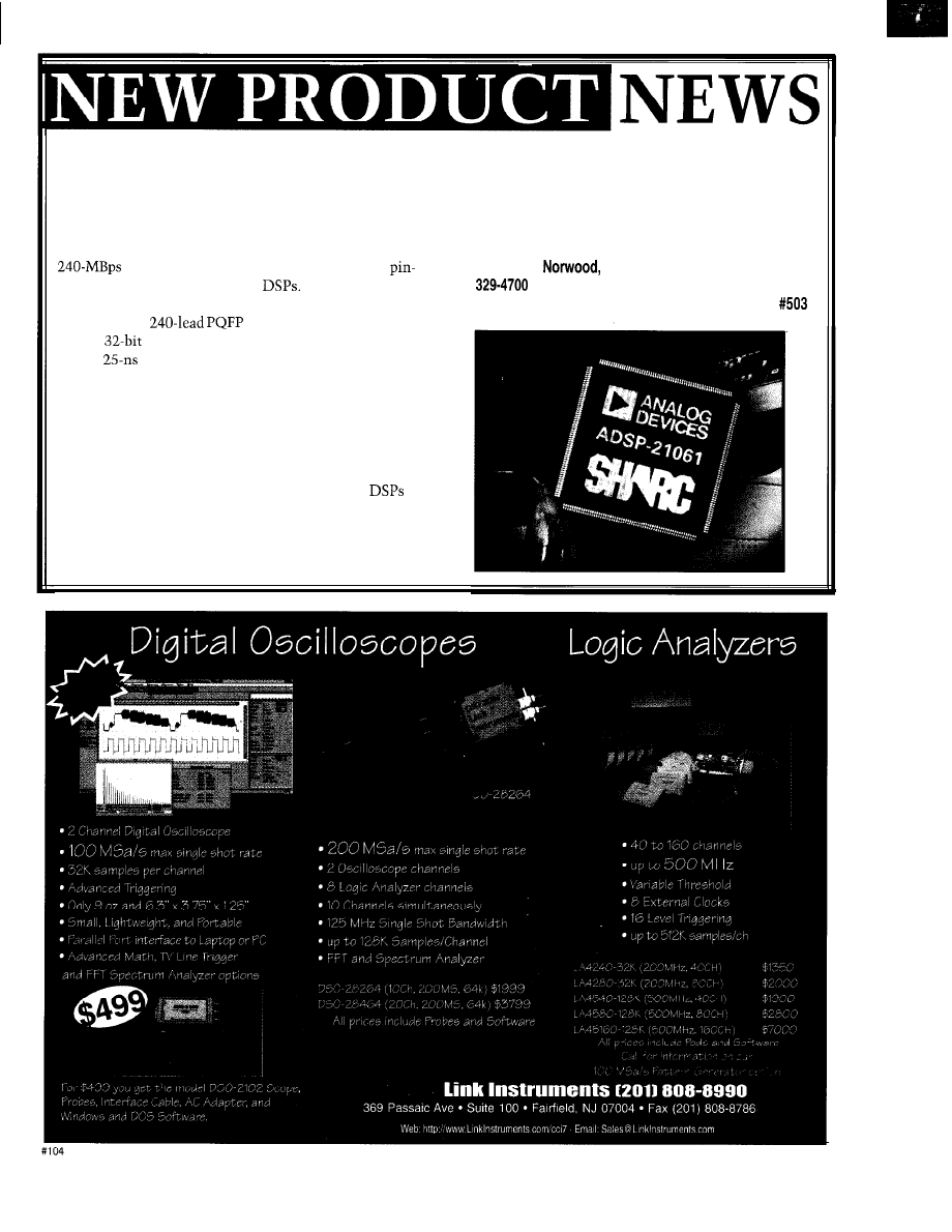
Analog Devices’ ADSP-21061 SHARC DSP features
Numerical C extensions in the C compiler enable easy
the same high-performance processor core as the current
coding and fast execution of vector and matrix operations.
SHARC DSP family but costs under $100. It has l-Mb
on-chip SRAM, six DMA channels, two serial ports with
Analog Devices, Inc.
I/O (40 Mbps bidirectional), and the same
P.O. Box 9106
l
MA 02062-9106
out as the ADSP-21060 and ‘62
It runs the same
(617)
l
Fax: (617) 329-1242
source code, operates from a +5-V power supply, and is
www.analog.com
packaged in a
(plastic quad flatpack).
The
floating-point DSP core runs at 120 MFLOPS
with a
instruction-execution time. Memory is
organized in two banks for both dual operand fetches and
independent core and DMA fetches. The dual-ported
memory enables all I/O to occur in parallel with the core
processing unit. The host/external port interfaces with
up to 4 Gwords of off-chip memory, other peripherals,
other SHARC processors in a cluster, and a host processor.
The EZ-Kit Lite development kit for SHARC
($179) offers a hardware platform and C compiler. The
tool set includes a ‘6 I-based add-in board, optimizing
ANSI C compiler, code compactor, assembler, linker,
loader, instruction-level simulator, and run-time library.
Circuit Cellar INK@
Issue
84 July
1997
9
FEATURES
Digital Generation of
Frequency Waveforms
Frequency Domain
Analysis with
DSP-Based Canadian
Receiver
David
Digital Generation of
High-Frequency Waveforms
n evaluating the
behavior of
processing or control
circuitry, it’s common to
use an analog function generator to
produce the necessary test input signals.
Typical cookbook waveforms are
used to investigate the circuit’s behav-
ior when stimulated by sine, square,
and triangle waves of different ampli-
tudes and frequencies.
In many applications, however,
repetitive sine, square, and triangle
waves seldom represent the signals the
equipment under test can process.
For example, the heart’s electrical
signal is a waveform consisting of a
complex mixture of these basic wave
shapes intertwined with intermittent
baseline segments.
Since a constant “live” feed of such
signals may be impractical or danger-
ous for testing biomedical equipment,
dedicated signal sources synthesize
waveforms like those generated by
their physiological counterparts.
Similar requirements are needed for
generating test signals of video, radar,
disk access, and other waveforms that
can’t be simulated by simple sines,
ramps, or square waves.
Today, nonstandard real-world
stimuli waveforms can be easily created
12
Issue 84 July
1997
Circuit Cellar INK@
Look-up Table
Address
Generator Circuit
Despite the concept’s sim-
plicity, a PC program that
copies digital values stored in
an array into a DAC severely
limits the maximum frequency
of spectral components for the
arbitrary signal. Even an as-
sembly program copying the
contents of sequential RAM
addresses to an I/O location
results in DAC writing rates of a few
megapoints per second at most.
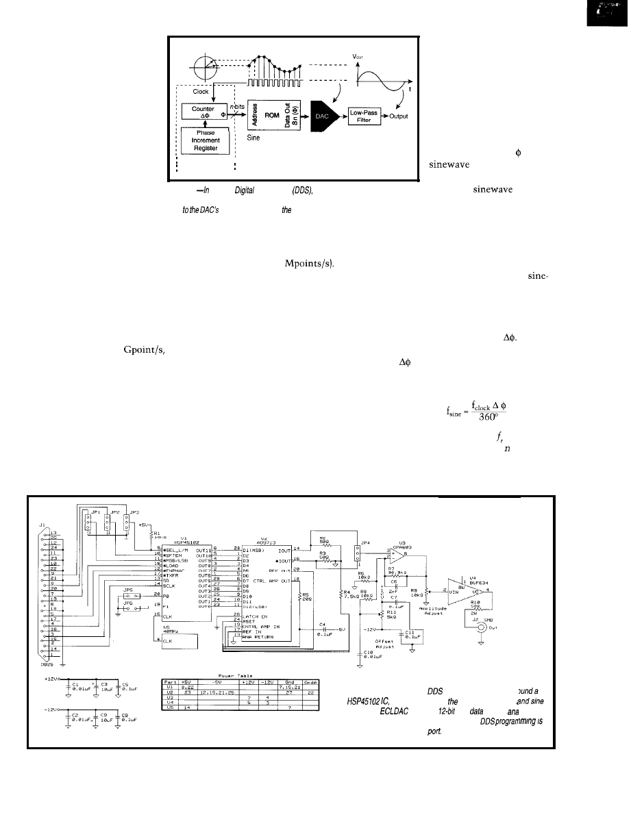
Figure 1
a Direct
Synthesizer
an address generator circuit or
phase accumulator controls how samples stored in a ROM lookup fable are deliv-
ered
input. Control over output frequency is achieved by selecting
an appropriate phase-accumulator increment.
signal has an amplitude resolution of
12 bits and variable temporal resolution
down to 50 ns (20
Obviously, if the clock presented to
the phase-accumulator counter remains
constant, then the phase-generation
rate does too. The end result is a
wave of a specific frequency.
as a numerical array and played
back through a DAC to yield
analog waveforms of arbitrary
complexity. This is the operat-
ing principle of an Arbitrary
Waveform Generator (arb).
Phase Accumulator
Instead of having a DAC interfaced
to memory through a processor, arbs
have dedicated RAM interfaced directly
to the DAC. So, update rates are lim-
ited only by the RAM’s access time and
the DAC’s speed. As such, commercial
arbs can be purchased with maximum
writing rates around
1
yield-
ing bandwidths of up to 500 MHz.
In this article, I discuss two simple
but versatile waveform generators that
can be programmed from a PC printer
port. The first is a circuit that generates
a sine wave by direct digital synthesis.
DIRECT DIGITAL SYNTHESIS
At its core, a generator that can
directly synthesize an analog signal
from digital data has memory contain-
ing the full digital time domain of the
desired waveform. To generate an ana-
log signal, the discretized point-by-point
version of the waveform is played se-
quentially through the generator DAC.
The second is an arb which, once
loaded with a digital-data array, acts as
a stand-alone instrument delivering
two simultaneous analog signals. Each
A simple form of this generator is a
Direct Digital Synthesizer (DDS). As
shown in Figure 1, an address-generator
circuit controls how samples stored in
ROM are delivered to the DAC’s input.
On each clock pulse delivered to the
address generator, a new address is
issued to the ROM so data
for the next point in the
sequence goes to the DAC.
The ROM in a DDS gen-
erator usually contains data
for a complete single cycle of
a sinusoidal waveform. The
address generator is a simple
counter. Its addresses make
up the phase angles of the
sin(@) samples in
ROM. A DAC translates into
an analog
the series
of values of this ROM look-
up table as a function of
incrementing phase angles.
However, DDS generators can vary
the sine output frequency without alter-
ing clocking frequency by programming
the phase increment value
If the
phase-accumulator output increments
by on each incoming clock pulse,
then the output sinewave’s frequency
is given by:
The frequency resolution of a DDS
generator is defined by the bits of the
phase-accumulator increment register
and the clocking frequency:
Figure 2-A simple and versatile
generator can be built an
Harris
which implements phase accumulator
look-up fable. An
converts
sine
info an
output, which is then filtered, buffered, and scaled.
performed through the PC printer
Circuit Cellar INK@
Issue 84 July 1997
1 3
Outputs:
Channel 1
2)
Computer
Digital Buffers
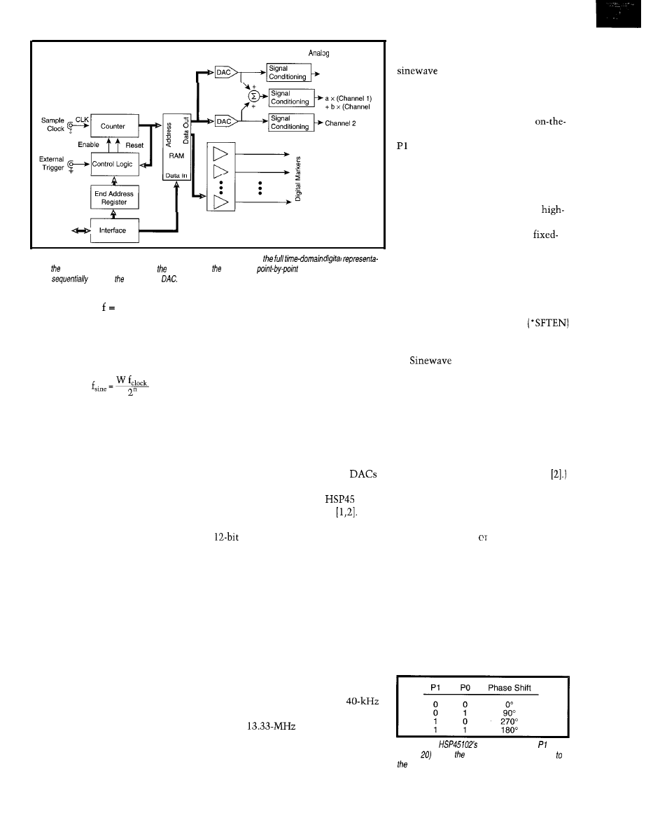
Figure 3-An arbitrary waveform generator has at ifs core a RAM containing
fion of desired waveform. To generate analog signal, discrefized
version of the waveform is
played
through generator’s
f
clock
I
2”
and the output frequency is directly set
by the value
W
of the phase-accumula-
tor increment register:
Since wide registers, large counters,
and ample ROMs are easily integrated,
IC DDS generators can now generate
sinewaves into the hundreds of mega-
hertz with incredibly high resolution.
In Figure 2, for example, a Harris
HSP45 102 IC implements the phase
accumulator and sine look-up table.
This 32-bit-wide phase-accumulator
increment register accepts clock fre-
quencies up to 40 MHz. So, the DDS IC
can provide data to generate sinewaves
from 0.009 Hz up to 20 MHz with a
resolution of 0.009 Hz!
The sinusoidal signal at the DAC’s
output is not infinitely pure. The digi-
tal samples translated by the DAC are
quantized in both time and amplitude,
so some distortion is introduced.
Obviously, time-quantization errors
are reduced by using as large a look-up
Time quantization results from the
fact that the signal can only change at
specific time intervals dictated by the
clock. Amplitude quantization results
from the discrete nature of the digital
system itself. Samples of the infinitely
continuous series of a sine are stored
in ROM with finite resolution.
14
Issue
84 July 1997
Circuit Cellar INK@
table as possible. For the HSP45102,
the look-up table is 8 192 samples wide.
Since the number of samples used to
reconstruct the sinusoidal wave is the
ratio of the clock frequency (40 MHz)
and the selected output frequency,
time-quantization errors worsen as the
selected output frequency increases.
Voltage-quantization errors, on the
other hand, are reduced by increasing
the width of the data word presented to
the DAC. Since price and complexity of
a high-frequency DDS circuit increase
with the DAC’s resolution, a number
of projects use only 8-bit video
to gain simplicity. But, that doesn’t
take full advantage of the
102’s
12-bit amplitude resolution
In the DDS circuit of Figure 2, a
TTL-input-compatible ECL DAC
makes full use of Ul’s data-word width.
High-frequency harmonics generated
by aliasing are low-passed by U3.
In more sophisticated systems, a
steep digitally-tuneable low-pass filter
passes the selected fundamental fre-
quency and rejects the sampling aliases.
The HSP45102 includes two 32-bit
phase-accumulator increment registers.
Using an appropriate low-pass filter
(e.g., an elliptic filter) is critical to get
clean output at high frequencies since
steps become increasingly large and the
DAC output resembles a sine-wave less
and less. For example, while a
output signal uses 1000 samples per
cycle, a
signal is generated
using barely 3 samples per cycle!
A digital input on pin 9 selects which
register is used at any given time for
generation, enabling direct
frequency-shift keying (FSK) modula-
tion of the output.
In addition, the DDS generator
enables the phase to be changed
fly by selecting the state of the PO and
lines (pins 19 and 20) as shown in
Table 1. This enables direct quadrature
phase shift keying modulation (
QPSK
).
These features open up tremendous
possibilities for DDS generators in
communications applications. A
stability carrier can be generated via
digital circuitry and a low-cost
frequency digital crystal oscillator, and
direct digital modulation is possible.
Program the HSP45 102 by loading
64 bits of data for the two phase-accu-
mulator increment registers through
the data input pin (SD) in serial format.
While keeping the shift-enable
pin low, each data bit is fed by a rising
edge on Ul’s clock input pin (SCLK).
generation is turned on
and off via the *ENPHAC pin. The
*TXFER input line controls the transfer
of the phase-accumulator increment
register selected by the SEL_L/*M line
(pin 9) to the phase accumulator’s
input register.
Here, I retained printer-port pin use
compatibility with a DDS generator.
(Control software is freely available
ARB BASICS
As you see in Figure 3, an arb shares
the basic building blocks of a DDS
generator. Instead a ROM sine look-
up table, however, a full time-domain
digital representation of the arbitrary
waveform is downloaded into RAM.
As well, the counter is not thought
of as a phase accumulator. You can
arbitrarily define the last data point of
the waveform cycle (end address). Thus,
the waveform can be replayed by loop-
ing from the last point to the address
of the RAM location for the first point.
Table l--The
input lines PO and (pins
19 and control introduction of a phase offset
phase accumulator’s output
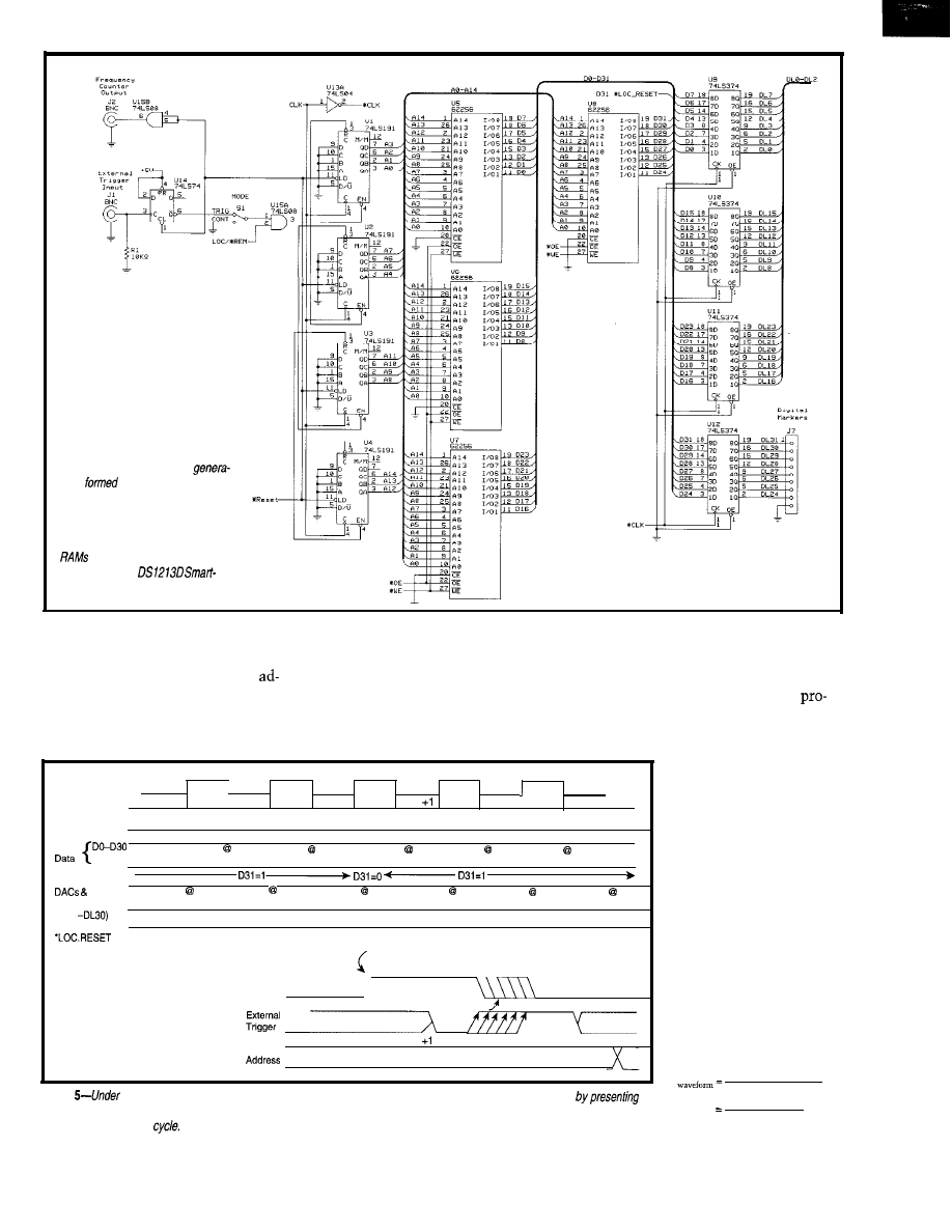
Figure 4-The arb’s address
for is
by a chain of synchro-
nous counters. At the end address, the
address generator resets, and the next
data latched to that of the first RAM
address. For nonvolatile operation, the
should be mounted on Dallas
Semiconductor’s
Sockets.
Clock
1
1
spectral components of
End Address
RAM
the waveform.
Address
End Address -1
End Address
Address 00
Reset
Address 01
Address02
Of course, reproducing
(DLO
U15 pin 3
(‘Counters Enable)
Triggered
Mode
End Address
RAM
End Address
Address 00
Address 01
ponent. In turn, the com-
plexity and time duration
of the reproduced wave-
form are limited by the
arb’s memory size (depth).
The output waveform’s
time duration is:
For some applications, the waveform
waveform sequence for every triggering
As well, instead of maintaining the
may be issued only once after a trigger
event. A typical application is the
clock-rate constant and jumping over
event. Additional circuitry in the
testing of ultrasonic echo systems,
sample points to change the period of a
dress generator receives a trigger signal
where the arb-generated echo must be
cycle, an arb’s clock frequency is
that allows addresses to be cycled once
synchronized to the excitation of the
grammable. Thus, the waveform can be
between the beginning and end of a
transmitting transducer.
compressed or expanded through time,
resulting in a controlled
shift in frequency of all
RAM
Data
Data
Data
Data
Data
a signal requires the stored
D31
End Address -1
End Address
Address 00
Address 01
Address 02
Data to
l
waveform to be sampled
Markers
Data
Data
Data
Data
Data
at a rate of at least twice
Data
End Address -2
End Address -1
End Address
Address 00
Address 01
Address 02
its highest frequency com-
Figure
operating conditions, the arb’s control logic ensures each waveform-sequence sample is equal/y long
the data contents only on the opposite edges of the clock than those causing address transitions. In the triggered mode, trigger ambigu-
ity is less than one clock
16
Issue 54
July
1997
Circuit Cellar INK@
T
# of
w a v e f o r m p t s .
f clock
end addr-
start&
f
clock
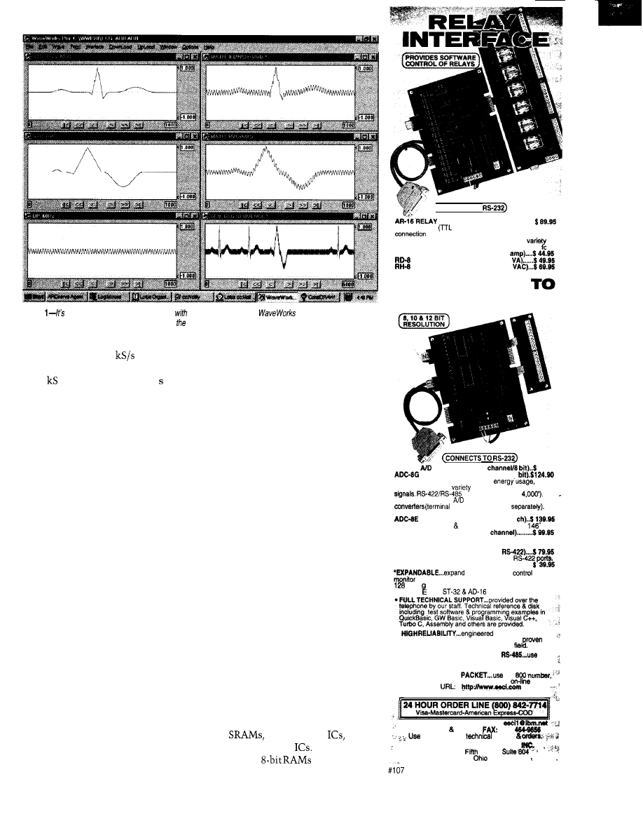
Photo
easy to create complex waveform
Pragmatic Instruments
Pro. Here’s a signal for
testing electrocardiography equipment by defining waveform’s basic components from predefined templates.
Speech, for example, requires a
sampling speed of -8
(where S
stands for samples). An arb with a depth
of 32 suffices for only 4.096 of
recording.
With fixed memory size, longer
waveform durations are only achieved
by limiting the bandwidth to allow
lower sampling rates. Obviously, limit-
ing the bandwidth reduces the number
of spectral components available to
describe the waveform’s details.
If an arb has more than sufficient
memory to generate a waveform, addi-
tional memory can be used for a second
waveform channel. Since both channels
are generated using a single clock, the
two output waveforms are precisely
synchronized. This capability is essen-
tial for testing instruments that derive
their measurements from the phase
relationship between two signals.
Also, purely digital lines (i.e., marker
channels) can synchronize and position
markers coincident with specified
points of the arb waveform. They can
trigger external instruments (e.g., oscil-
loscopes) at specific times within the
arb waveform cycle.
However, an additional channel’s
greatest advantage is the possibility of
summing both channels. Two synchro-
nized arbitrary components of a single
waveform can be independently con-
trolled, making it possible to test the
effect of each system component.
To study a circuit’s immunity to an
unwanted phenomenon, channel
1 can
be loaded with the waveform normally
seen by the system under test. Channel
2 can be loaded with the anomaly at the
desired time within the normal wave-
form. By varying the gain of channel 2,
you can adjust the anomaly’s amplitude
without changing the amplitude of the
normal signal.
Summing arb channels extends the
dynamic range of the combined signal
beyond the maximum dynamic of each
independent channel. Altering the gain
of the summed channels makes it
possible to generate large signals with
very small features on them.
Here, macroscopic changes occupy
the full dynamic range of one channel.
The smaller waveform details occupy
the other channel’s full dynamic range.
By correctly ratioing the gains between
the channels, the summed signal can
have a theoretical maximum resolution
equal to the sum of the independent
channels’ resolutions.
PC-PROGRAMMABLE ARB
A simple arb can be built with stan-
dard
a few counter
some
glue logic, and DAC
In this project,
three 32 K x
store two
(CONNECTS TO
INTERFACE (16 channel) . . . . . . . . . . . .
Two 8 channel
level) outputs are provided for
to relay cards or other devices (expandable
to 128 relays using EX-16 expansion cards). A
of
relays cards and relays are stocked. Call for more i n o.
AR-2 RELAY INTERFACE (2 relays, 10
REED RELAY CARD (6 relays, 10
RELAY CARD (IO amp SPDT, 277
A N A L O G
D I G I T A L
ADC-16
CONVERTER” (16
99.98
AID CONVERTER* (6 channel/IO
Input voltage, amperage, pressure,
light,
joysticks and a wide
of other types of analog
available (lengths to
Call for info on other
configurations and 12 bit
block and cable sold
Includes Data Acquisition software for Windows 95 or 3.1
TEMPERATURE INTERFACE’ (6
Includes term. block 8 temp. sensors (-40’ to
F).
STA-6 DIGITAL INTERFACE’ (6
Input on/off status of relays, switches, HVAC equipment,
security devices, keypads, and other devices.
PS-4 PORT SELECTOR (4 channels
Converts an RS-232 port into 4 selectable
CO-422 (AS-232 t o RS-422 converter) . . . . . . . . . . . . . . . . . . .
your Interface to
and
up to 512 relays, up to 576 digital inputs, up to
anal0
the PS-4.
inputs or up to 128 temperature inputs using
X-16,
expansion cards.
l
for continuous 24
hour industrial applications with 10 years of
performance in the energy management
l
CONNECTS TO RS-232, RS-422 or
with
IBM and compatibles, Mac and most computers. All
standard baud rates and protocols (50 to 19,200 baud),
FREE INFORMATION
our
Fax or E-mail to order, or visit our Internet
catalog.,.
Technical Support (614) 464-4470
I n t e r n e t E - m a i l :
International Domestic
(614)
for information.
support
ELECTRONIC ENERGY CONTROL,
380 South
Street,
Columbus,
43215-5491,
Circuit Cellar INK@
Issue 84 July 1997
1 7
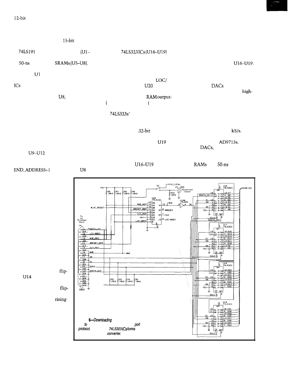
waveforms. An additional RAM
IC provides 7 marker channels, and the
additional bit encodes the last valid
data sample of a waveform sequence.
As Figure 4 shows, the
address
generator of the arb is formed by a chain
of
synchronous counters
U4). The counter chain’s output is sent
to
access-time
From the timing diagram in Figure 5,
as long as
is enabled, each clock
pulse supplied in parallel to all counter
advances the address. This process
continues until the address points to a
The arb’s circuitry ensures that each
sample of the waveform sequence has
data element (D31) on
in which
equal length. Data contents presented
on the RAM data bus (DO-D30) are
bit 7 is low, causing the asynchronous
latched on edges of the clock opposite
to those causing address transitions.
reset of the counter chain.
(where bit 7 of
is
low) resets address to zero
without upsetting the data
related to END-ADDRESS.
Since the data at the output of
latches
lags the data of their
inputs by half a clock cycle, the reset
signal issued when the counters reach
The clock line’s next
falling edge causes the data
contents of the first RAM
address to be sent to the
latches’ output. While the
trigger ambiguity is less than one clock
cycle.
A simple, software-implemented
serial protocol downloads and uploads
RAM waveform data from and to the
PC through the printer port. On the arb,
the chain of
of
Figure 6 forms a 32-bit serial-to-paral-
lel and parallel-to-serial converter.
When the remote mode is selected
by the computer (digital low on bit 1 of
the printer port’s output port),
*REM goes low, causing
to trans-
The
mode-control lines
fer control of the clock (CLK), address
(pins 1 and 19) select between hold,
shift left or right, and parallel load of
generator reset (*RESET),
the bits of the chain’s
register.
Data is clocked serially into U16 and
shifted down the chain towards
by
enable
l
OE), and RAM write
l
WR) to
each rising edge of the serial clock line
(SCLK).
the lines of the printer port.
RAM data bus and a write strobe stores
Once a complete 32-bit word is in
the chain’s register,
drive the
the register’s contents in the current
address. The address generator ad-
vances, and the cycle repeats to store
successive waveform data points. Data
can be read from RAM into the com-
puter by reversing this process.
Once an address is selected, data
loads from the RAM data bus into the
register formed by the chain
The register’s contents are then shifted
out of U16 into one of the printer port’s
status input lines (pin 10 of J4).
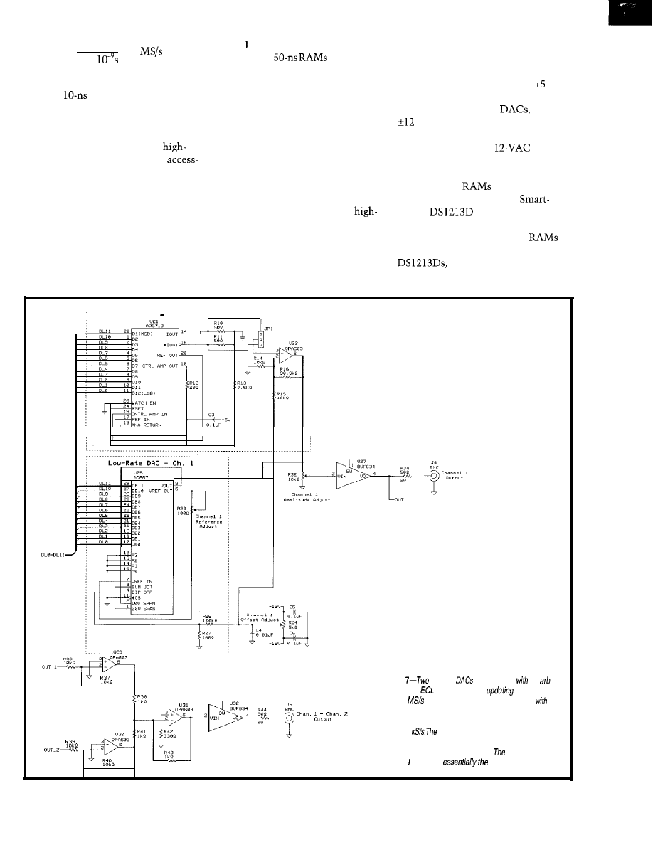
Two different
work with the
arb. An Analog Devices AD9713
speed ECL DAC capable of updating
its output at up to 100 MS/s restores
high-frequency signals with high reso-
lution [see Figure 7). Alternatively, the
lower cost AD667 offers more limited
performance for applications with DAC
writes of no more than 300
allow a maximum writing speed of:
Unfortunately, it’s difficult to take
full advantage of the
With
high-speed
the arb’s speed is
limited by the RAM’s access time.
Under this arb’s direct addressing archi-
tecture,
with
access time
time that the first address is
available is shorter than for
any other address, the corre-
sponding data is available at
the output for the same
amount of time as other
addresses.
When triggered, rather
than continuously cycling
through the waveform,
flop
controls Ul’s en-
able line via switch S 1. In
the triggered mode, the
flop’s
l
Q output goes low
when enabled by the
edge of a trigger pulse at its
clock input line.
This state is maintained
until reset at the end of the
waveform cycle by the same
reset pulse that zeroes the
counter chain. In this mode,
Figure
and uploading RAM waveform data from
and the PC is done through the printer
under a simple serial
The chain of
a 32-M serial-to-parallel
and parallel-to-serial
1 8
Issue 64 July 1997
Circuit Cellar INK@
1
50 x
= 20
Achieving 100 MS/s writing speeds
requires
RAM
S
. Although they’re
available [e.g., cache RAM], they are
very costly, limited in size, and gener-
ally power hungry. Rather than using a
direct addressing scheme, very
speed arbs overcome the RAM’s
time shortcomings by operating several
RAM banks in parallel.
In this multiplexed address scheme,
one or more RAM banks are accessed
and allowed to settle while current
data is taken from a different RAM. As
the address updates, data is taken from
a RAM that already has valid data
available.
A 4: multiplexed memory arb uses
four low-cost
to achieve
80 MS/s. I decided against the more
complex multiplexed approach since
20 MS/s provides sufficient flexibility
in generating relatively low-frequency
signals to test biomedical instruments.
Once analog signals are at the DAC
outputs, the circuit offsets and scales
them prior to buffering them for out-
put. A summing channel is also pro-
vided to expand the arb’s versatility.
The local sampling clock is gener-
ated by U33, Maxim’s MAX038
frequency waveform generator IC.
Although this IC typically acts as a
function generator, in Figure 8, it’s an
oscillator whose frequency can be con-
trolled from 20 Hz to 20 MHz. Alterna-
tively, the sampling clock may be sup-
plied by an external TTL-level clock
through connector J3 and switch S2.
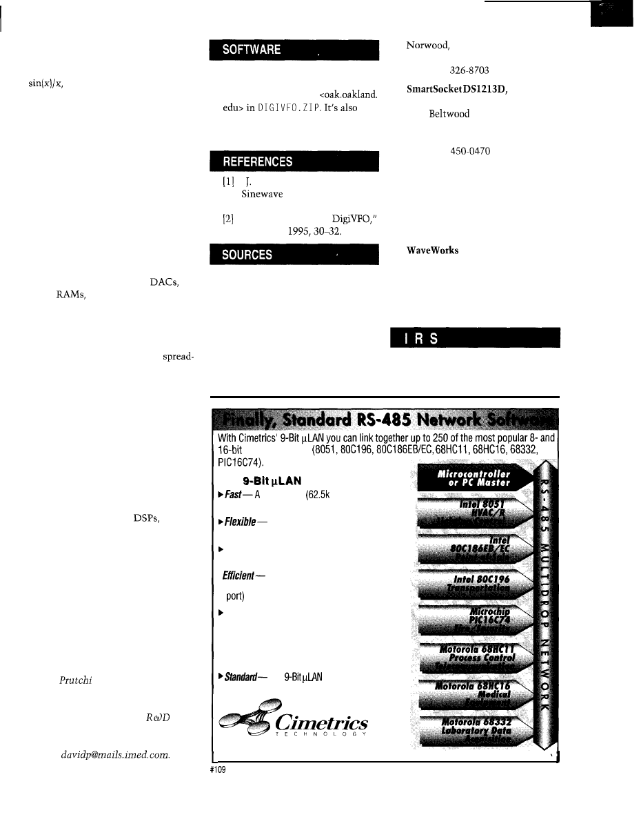
The arb’s circuitry requires V for
the logic circuitry, -5 V for the ECL
logic of the high-speed
and
V for the analog circuitry. The
power supply in Figure 9 generates
these voltages from a
input.
The arb loses waveform data as soon
as power is removed. For nonvolatile
operation, the
may be mounted
on Dallas Semiconductor’s
Socket
intelligent sockets.
Remember, these sockets are. de-
signed to be compatible with
of
up to 128 K x 8. So, when using the
you need four more PCB
pads than those required for each RAM
High-Rate DAC Ch. 1
Figure
different
can
be used
the
A high-speed
DAC capable of
its output at
up to 100
can restore high-frequency signals
high resolution. A lower-cost DAC provides more limited
performance for applications that require writing speeds
of up to 300
DAC analog outputs are then
offset
and scaled as needed. In addition, a summing
channel expands the arb’s versatility
schematics for
channels and 2 are
same.
Circuit Cellar INK@
Issue 84 July 1997
19
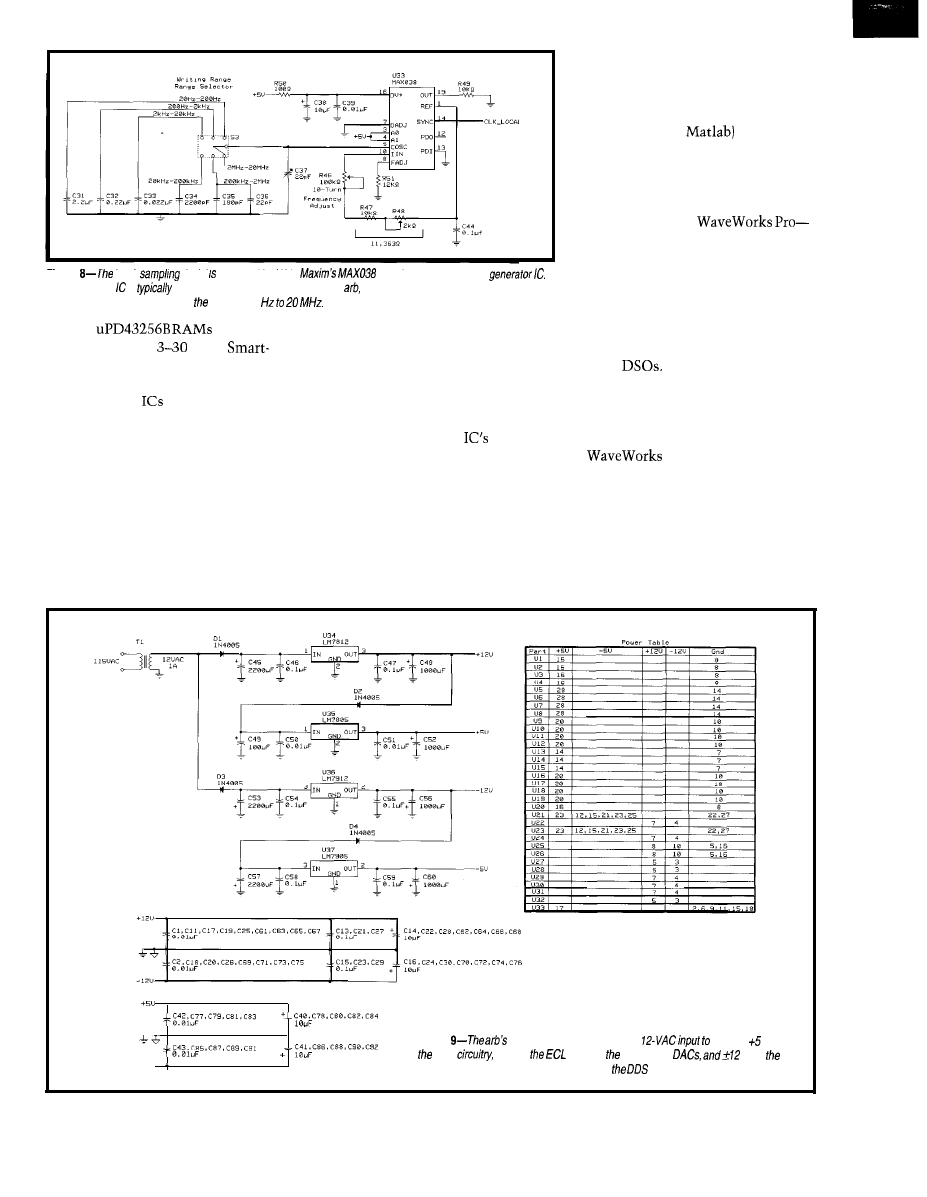
Figure
local
clock generafed by U33,
high-frequency waveform
Although
this is
used as a function generator, within fhe
if functions as a clock oscillator whose
frequency can be controlled over range of20
IC. The
are then
mounted on pins
of the
Sockets.
You could also use Dallas Semicon-
ductor DS1210
to handle RAM
power backup from a small battery [see
Jeff Bachiochi’s “Creating a Nonvola-
tile RAM Module,” INK 16).
Last, a word of caution. High-fre-
quency clocks and signals demand
proper layout techniques (see “Design-
ing Printed Circuits for High-Speed
Logic,” INK 42).
Preferably, use a multilayer PCB.
Separate the analog ground from the
digital ground, and join them at a single
point at the power source.
Be sure to keep interconnection
over the buses short and equal. In
addition, use good-quality high-fre-
quency capacitors to decouple the
power rails close to each
power
input pins.
ARBITRARY WAVEFORMS
Signal creation for reproduction by
an arb is usually done by capturing an
analog signal using a digital storage
oscilloscope (DSO) or creating the
waveform on a PC via a numerical
representation of the waveform’s
mathematical formulation.
In the latter case, although short
BASIC programs or numerical process-
ing packages (e.g.,
can generate
waveform data, truly flexible waveform
creation is possible only through dedi-
cated software.
One of my favorite packages-prag-
matic Instruments’
offers an intuitive environment for
waveform creation from a comprehen-
sive menu of standard templates, math
operations, and transfer functions.
Waveforms can also be imported
from other programs or directly up-
loaded through GPIB or RS-232 from
popular
Waveform synthesis
and analysis can be performed either in
the time or frequency domains.
They provide immediate solutions
for generating test waveforms for gen-
eral-purpose applications (e.g., sinusoi-
dal, square, triangular waves, etc.),
communications testing (e.g., AM, FM,
Photo 1 shows how easy it is to
create waveforms with a package such
as
Pro. The software has
30 standard waveshapes with program-
mable parameters.
Figure
linear power supply requires a
produce V for
logic
-5 V for
logic of high-speed
V for
-5”
analog circuitry. The same circuit can power
generator.
20
Issue
84 July 1997
Circuit Cellar INK@
BFSK, QPSK, NTSC waveforms, etc.),
as well as other signals for advanced
signal processing and control (e.g.,
ECG waveform, digital and
analog noise, etc.).
After a waveform is defined, it can
be modified using the 20 predefined
transfer functions or I3 mathematical
operators. Once the desired waveform
is created, an FFT-based spectral esti-
mator offers frequency analysis with
the possibility of spectral editing and
IFFT-based transformation back into
time-domain.
A long, complex waveform can be
created by looping and seamlessly
linking previously created waveforms.
MORE FOR YOUR MONEY
As faster high-resolution
wider
and higher performance
processors enter the market, digital
waveform generators are rapidly re-
placing analog sources.
High-performance integrated DDS
generators have taken over the
spectrum communications field. They
enable low-cost cable modems bring-
ing you super-high-speed access to the
‘Net from home.
Arbs are also becoming popular with
design and test engineers, and they’re
more versatile sources than their analog
counterparts. In fact, even with stan-
dard waveforms, arbs can compete
with analog generators.
Of course, the neat control and
waveform-design screens of commer-
cial arbs, their powerful
and
exotic high-frequency mixed-mode
circuitry make them costly pieces of
equipment. Most range from $3000 to
$7000, whereas an analog signal gen-
erator with similar bandwidth costs
just a few hundred dollars.
So, don’t feel your reliable analog
waveform generator doesn’t deserve
space on the workbench. Just keep the
arb in mind when you demand ultimate
flexibility and lots of performance.
q
David
has a Ph.D. in Biomedi-
cal Engineering from Tel-Aviv Univer-
sity. He is an engineering specialist at
Intermedics, and his main
inter-
est is biomedical signal processing in
implantable devices. You may reach
him at
Software compatible with the DDS
generator in this article is available
at the ARRL ftp site at
available on the Circuit Cellar Web
site.
R. Portugal, “Programmable
Generator,” Electron-
ics Now, January 1995, 43-66.
J. Craswell, “Weekend
QST, May
HSP45102
Harris Semiconductor
1301 Woody Burke Rd.
Melbourne, FL 32902
(407) 724-3000
Fax: (407) 724-3937
AD9713
Analog Devices, Inc.
One Technology Way
MA 02062
(617) 329-4700
Fax: (617)
DS1210
Dallas Semiconductor Corp.
4401
Pkwy. S
Dallas, TX 75244-3292
(214) 450-0448
Fax: (214)
MAX038
Maxim Integrated Products, Inc.
120 San Gabriel Dr.
Sunnyvale, CA 94086
(408) 737-7600
Fax: (408) 737-7194
Pro
Pragmatic Instruments, Inc.
73 13 Carroll Rd.
San Diego, CA 92 121
(619) 271-6770
Fax: (619) 271-9567
401 Very Useful
402 Moderately Useful
403 Not Useful
microcontrollers
The
Is:
high speed
baud) multidrop
master/ slave RS-485 network
Compatible with your
microcontrollers
Reliable- Robust 16-bit CRC and sequence
number error checking
.
Low microcontroller resource
requirements (uses your chip’s built-in serial
Friendly- Simple-to-use C and assembly
language software libraries, with demonstration
programs
. Complete- Includes network software,
network monitor, and RS-485 hardware
The
is an asynchronous
adaptation of IEEE 1118
55 Temple Place
l
Boston, MA 02111-1300
l
Ph 617.350.7550
l
Fx 617.350.7552
Circuit Cellar INK@
Issue 84 July 1997
21
William Hohl
Joe
Frequency Domain Analysis
with
e Carter
like a big,
with two large cups for hold-
ing your telephone handset. It could
have been a prop in a Lost in Space
episode. Of course, that was back when
punch cards were the cutting edge in
storage media.
Today, a modem is almost nothing
more than a piece of software running
on a dedicated DSP or the newest pro-
cessor with multimedia extensions.
In embedded applications,
are
quickly replacing their analog counter-
parts as consumer electronics integrate
voice/data and graphics capabilities in
everything from telephones to automo-
tive displays.
Now that technology is able to
actually implement some of those gory
algorithms you ignored in college, more
applications are starting to use
orthogonal transforms (remember
Fourier?) and IIR filters, for example.
In embedded environments, how-
ever, there’s a tradeoff between the
amount of functionality you can assign
the controller and the amount of board
space you have for dedicated proces-
sors. Multiple-chip solutions are ex-
pensive.
A processor providing both the
control functions and the necessary
signal processing would be a great
benefit to such designs.
Enter Motorola’s
Its archi-
tectural design specifically targets the
emerging applications in advanced
consumer electronics.
Its core is small enough to easily
add on-chip memory, peripherals, and
other system modules while remaining
cost effective As you know, in
driven embedded systems, memory
can sometimes end up costing more
than the processor.
Since the
ISA is based on
the
it retains a high-density, vari-
able-length instruction set that maxi-
mizes code density and keeps memory
requirements down. Its architecture
and implementation philosophy are
flexible enough that different configu-
rations within the core are also pos-
sible.
As for signal processing, the addition
of a new multiply-accumulate (
MA
C)
engine within the core supports a lim-
ited set of DSP operations that creep
up in today’s embedded applications. It
also supports the existing multiply
instructions already in the architec-
ture-just more quickly.
In this article, we examine
Fire’s processor core, the MAC unit,
and transforms used in signal process-
ing, and we show how it all fits to-
gether.
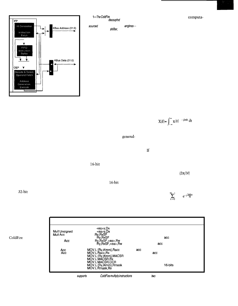
PROCESSOR CORE
Let’s start with a look at the V.2
processor core. It features two indepen-
dent, decoupled pipeline structures
that maximize performance while
minimizing core size [see Figure 1).
The Instruction Fetch Pipeline (IFP)
is a two-stage pipeline for prefetching
instructions. The instruction stream is
then gated into the two-stage Operand
Execution Pipeline (OEP). This de-
codes the instruction, fetches the re-
quired operands, and executes the
function.
The OEP includes the two standard
execution units-a barrel shifter and
the main ALU. The new MAC unit
resides in the OEP and resembles an-
other execution unit to the core. Each
unit is a three-ported device that takes
two operands as input and generates a
result.
22
Issue 84 July 1997
Circuit Cellar INK@
THE MAC ENGINE
Before designing a new execution
block, Motorola decided that redesign-
ing the wheel wasn’t a hot idea. The
goal wasn’t to create another DSP from
the 68k architecture. However, they
did want engineers to be able to imple-
ment a variety of DSP routines for
practical applications.
To strike a middle ground between
speed, size, and functionality, the new
MAC unit implements a three-stage
arithmetic pipeline containing a multi-
plier array followed by adder logic.
Since multiplier arrays can chew up
silicon in a hurry, the MAC unit is
optimized for 16 x 16 multiplies with a
possible accumulation cycle to follow.
At the expense of a little extra control
logic,
operations are still sup-
ported.
The new MAC instructions provide
for the multiplication of two numbers,
followed by the addition or subtraction
of this product to or
from the accumulator’s
value (see Table 1).
Some of the truly
useful additions to the
architecture
come from new in-
structions that enable
an operand fetch in
parallel with a MAC
operation. This results
in an overall perfor-
mance increase for
operations like convo-
lution and filtering.
Figure
V.2 core consists of
two
independent and
pipeline
stages. Once in the Execute stage, operands
are
to one of three execute
the main ALU, a barrel
or the MAC unit.
The product can also be shifted
1 bit to the left or right before
addition or subtraction takes
place. For situations where you
might use saturation arithmetic
(e.g., in a filter with input values
that may not be within the range
you expected), a bit in the MAC
unit’s status register enables or
disables saturation on an over-
flow.
The MAC engine is pipelined, so
you can issue MAC instructions once
every clock for word-length operations
and once every three clocks for long
operations. Since only the MAC unit
sees the value in the accumulator, an
additional
move
instruction is necessary
to transfer data to and from a
purpose register.
You can also choose which word
you want in a long word during calcu-
lations. This feature is extremely use-
ful for DSP operations, since you can
load two
coefficients into one
register and two 16-bit data samples
into another.
Alternating the word choice means
you can perform two
MAC op-
erations without fetching additional
operands between instructions.
TRANSFORMS
Embedded processors are getting
smaller, faster, and smarter. You can
now implement a number of
tionally intensive algorithms that were
relatively uncommon in embedded
code.
While we’re not talking about rou-
tines that make your toaster talk,
there are some fairly common algo-
rithms (e.g., orthogonal transforms)
that convert time-domain signals into
the frequency domain.
In this article, we discuss two trans-
form implementations-one for the
Discrete Fourier Transform (DFT) and
one for the Discrete Cosine Transform
(DCT).
DISCRETE FOURIER TRANSFORM
Let’s look first at the DFT. Think
back to that partial differential equa-
tions course you took in college. If you
recall, for a continuous-time signal x(t),
the Fourier transform is defined as:
e
and in general, x(t) is a complex func-
tion. A discrete-time signal x(n) is
created by sampling the continuous
waveform x(t).
we restrict the length of the se-
quence
x(n)
to n samples and we as-
sume that the signal is periodic outside
that range, then the Fourier transform
becomes discrete with the distance
between samples being
in nor-
malized frequency units.
So for a discrete sequence
x(n),
the
forward transform winds up as:
X
(k) =
x (n)
For years, a number of new and
interesting approaches have been taken
Operation
Mnemonic
Description
Mult Signed
Multiply
with Load
Load
Store
Load MAC Status Reg
Store MAC Status Reg
Move MACSR to CCR
Load Mask Reg
Store Mask Reg
MULS
MULU
MAC
MSAC
MAC
MSAC
Multiplies two signed operands, signed result
Multiplies two unsigned operands, unsigned result
Multiplies two unsigned/signed operands, then adds/
subtracts product to/from
Multiplies two unsigned/signed operands, then adds/
subtracts product to
while loading a reg with
memory operand
Loads
with 32-bit operand
Writes contents of
to a reg
Writes a value to MAC status reg
Writes contents of MAC status reg to a reg
Writes contents of MAC status reg to processor’s CCR
Loads mask reg with lower
of operand
Writes mask reg to a reg
Table l--The
MAC unit
the existing
and provides the
new MAC commands. A new feature in the
architecture can load data in parallel with the MAC instruction.
Circuit Cellar INK@
Issue 84 July 1997
23
DFT
Figure
flow graph for an eight-point
shows the
iterative
nature. Notice
input
is sequential, whereas
output is in bit-reversed order.
to
reduce the computational require-
ments to implement this equation.
Most try to exploit the properties of
the phase (or twiddle) factors:
Such methods include the Goertzel
algorithm
the chirp z-transform
method, and other flavors involving
convolution.
The more popular Fast Fourier
Transform-the Cooley-Tukey algo-
rithm-has a fairly lengthy history, so
we’ll only examine it from the point of
the signal-flow graph.
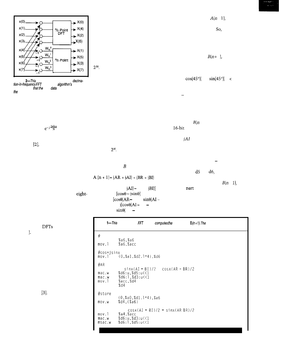
In Figure 2, a decimation-in-fre-
quency algorithm is shown for an
point transform. You can see that the
output X(k) is successively divided into
smaller and smaller subsequences. For
this case, there are three stages of
calculation, and each stage computes
four two-point
or butterflies (see
Figure 3
How do you implement this? First,
consider the amount of memory you
have, the processor speed, and the
application’s limitations. Obviously, if
you have a time-critical application,
you may have to use extra memory
and straight-line code the algorithm.
The source code presented here for
the FFT routine implements the famous
triple-nested DO loop for a complex
128-point FFT
It has a small code
size but not the fastest execution time.
Second, you have to decide on a
data format. Floating-point formats are
messy, and having your binary point
wander all over the place makes the
bookkeeping tedious. Plus, you have
to worry about overflow conditions.
24
Issue 84 July 1997
Circuit Cellar INK@
So for this example, the data is
assumed to be in a fixed-point fractional
notation, where the most significant
bit represents the sign of the number
and the remaining bits represent digits
behind a binary point.
In other words, you find the decimal
value by treating the 16-bit field as a 2’s
complement number and dividing it by
This implies, however, that the
number 1 .O can’t be represented by
this notation.
But, such is life. We can work around
this.
When working with fixed-point
numbers, overflow is a definite possi-
bility. That is, you cannot represent
the product of your two numbers using
only 32 bits. To deal with these cases,
use interstage scaling so that at each
stage of the FFT calculation, the out-
put is divided in half.
Specifically, for M stages, you end
up with the final results X(k) scaled
down by
Why is this necessary?
If you examine the results at each
stage of the calculation, the newest
values of A and are found by:
= (AR + BR) + j (AI + BI)
B (n + 1) = [(AR +
(BR +
=
BR) +
BI)]
+
BI)
AR BR)]
For the value of
+ the sum of
the imaginary or real parts can produce
a value greater than
1.
the values
AR, BR, AZ, and BZ are all scaled down
by a factor of two before they get used.
This way, the sums are guaranteed to
be realizable in this fractional notation.
For the output
1
the largest
value that either the real or the imagi-
nary values could have is:
1) +
1) 2
So, if the difference terms, such as
(AR BR), are already scaled down by a
factor of two, the largest value‘for the
sum is guaranteed to be less than 1.
Listing
1
offers the assembly code
calculating the real and imaginary
values for
+ 1). In this example, the
values are stored sequentially.
For example, the complex value
AR +
is
contained in one long-word
operand. Each coefficient (twiddle
factor) is also stored in memory with
real and imaginary halves.
The difference (AR BR) and the
sum (AR + BR) have already been stored
in registers and
respectively,
and scaled down by a factor of two.
For the real portion of
+ the
cosine
of the twiddle factor is
chosen with the upper/lower word
select, then multiplied by the differ-
ence and shifted one bit to the left
with one MAC instruction.
Listing
section of fhe
routine
new value of
real
and imaginary
portions of each operand are stored sequentially and fhe operands are considered fractional values.
clear MAC's accumulator
sub.1
#start bottom of butterfly
gets loaded first
and BR have already been prescaled
#calculate
+
swap
BR to memory
lea
#calculate
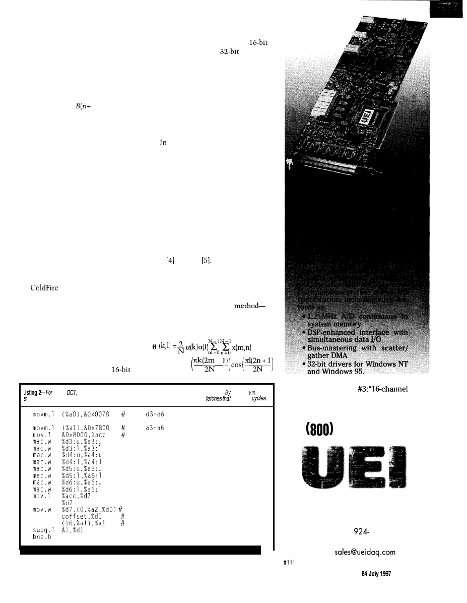
That left shift realigns the binary
point and removes the extra sign bit.
You get the sine portion in a similar
way. This value is then added to the
value already in the accumulator.
A final store of the accumulator to
a general-purpose register lets us move
the results out to main memory. The
imaginary part of
1) is found in
much the same way as the real part.
As we mentioned, the code for the
entire FFT routine is written as a set of
nested loops. The outer loop controls
which stage of the FFT you’re in.
A second, inner loop determines the
step size needed for pointing at the
right set of values to use.
The innermost loop does most of
the work. Since the two-point butter-
fly sits inside this loop, you obviously
want to minimize the number of cycles
spent calculating it.
You can use a few tricks to reduce
both the cycle time and the instruction
count inside of tight loops.
For example, normally you might
be tempted to just move zero into an
address register to clear it. However, in
the
ISA, this instruction
would occupy two words and could
force two instruction fetches if it sits
on a funny boundary.
A better approach is to subtract the
register from itself. It’s a one-word
opcode, and it does the same thing in
one cycle.
Another operation to watch for is a
multiplication involving two
signed numbers, such as the ones we’re
using. When you multiply two
numbers to produce a
result, you
end up with an extra sign bit. A left
shift is needed to keep the binary point
in the correct spot.
Here’s where the optional shift on a
MAC instruction is useful. You can
realign the data before adding it to the
accumulator, saving another cycle.
DISCRETE COSINE TRANSFORM
the next transform example, we
look at a two-dimensional Discrete
Cosine Transform (DCT).
This transform has been used for
data compression in a number of differ-
ent standards, including CCITT Rec.
H.261, the JPEG standard for still im-
ages, and the MPEG standards for
video.
There are several efficient ways to
implement this algorithm. Over the
years, a number of fairly clever rou-
tines have emerged, such as those by
Hou and Lee
In fact, you can show that the algo-
rithm for computing the DCT looks
like the one for computing the FFT.
However, for the purposes of illustra-
tion, we use a more direct
the matrix formulation.
A two-dimensional DCT is given
by:
x
cos
+
the
one vector of data is calculated by successive MAC operations. using mo data
quickly loaded info four genera/-purpose registers first, avoiding any later operand
may add
load
with source data
loop_one:
load
with coeff data
rounding value
swap
output rearranged for next pass
add.1
on first pass, add 16, else add 0
lea
always add 16
loop-one
{Second in a continuing
series.
iook for Reason
on-board simultaneous sampling.‘)
Call today for your free catalog:
829-4632
United Electronic Industries
10
Dexter Ave, Watertown,
MA 02 172
Tel:
Fax:
internet:
E-mail:
Circuit Cellar
INK*
(6 17) 924-l 155
(6 17)
144 1
www.ueidaq.com
I s s u e
27
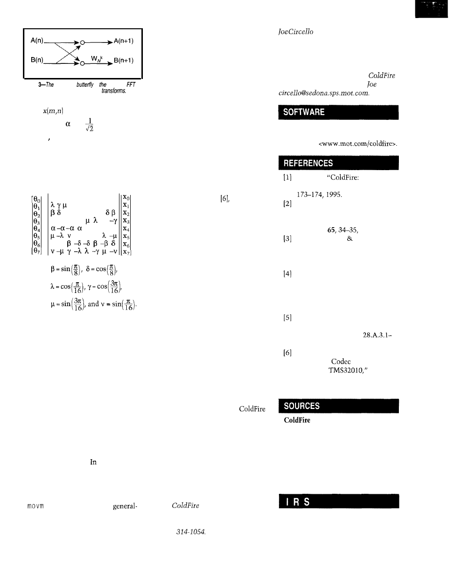
- 1
Figure
two-point
is simplest
and the basic building block of larger
where
is an N x N field and
(k) =
fork = 0 unity otherwise.
The input in this case might be
something like an 8 x 8 block of pixel
data from an image. If the DCT is
carried out with a matrix formulation,
then the routine is based on:
1 1 1 1 1 1 1 1
v - v - p - y - h
- s - p - p - s
y - v - h - p v
=
a-a-a a
y - y - v
s-p
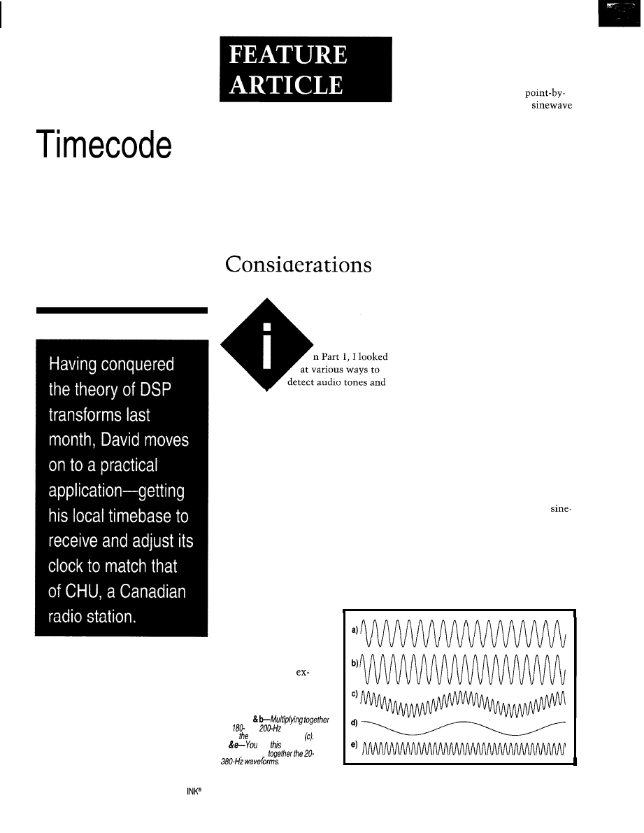
where:
To calculate the entire transform,
you have to perform the above opera-
tion 64 times. Since the DCT kernel is
separable, the two-dimensional trans-
form can be done in two passes-first
along the rows of the input matrix,
then along the columns.
In this implementation, a separate
matrix to hold the transposed data isn’t
needed before the second pass. The
operands are stored in memory in their
transposed positions during the first
pass.
Eight small loops comprise the bulk
of the DCT routine (one is shown in
Listing 2). Each loop calculates one
vector of output data. this imple-
mentation, all the coefficients and
data samples are word-length operands.
Instead of fetching two operands to
multiply and accumulating the result,
a
instruction loads four
purpose registers with all eight data
samples. Another
movm
loads four more
registers with all eight coefficients.
The MAC instructions are done in
series, effectively one per clock. Using
the upper/lower word select bit, you
can perform two MAC operations with
the same registers. The accumulator is
then transferred to a general-purpose
register and moved out to memory.
The format of the coefficients is
similar to that of the FFT routine. In
other words, the binary point is as-
sumed to be after the first bit and the
remaining bits are the fractional value.
The input data is an integer value
and, depending on the image, can be
between 0 and 255. During the inter-
mediate multiplications, only the
integer portion of the results are kept
[the upper
16
bits).
Using a technique similar to the
one by Srinivasan et al
a rounding
value is added at the beginning of the
routine to account for round-off errors
and truncation.
FINDING YOUR SOLUTION
These algorithms are intended as
illustrations, not actual concrete solu-
tions. While they provide a working
model, certain enhancements speed up
execution times (e.g., using caches or
storing some data blocks in on-chip
RAM instead of external memory).
Depending on the DSP problems
you want to solve, you might find
yourself looking for a fast predictive
filter, another type of transform, or
just a run-of-the-mill FIR filter. We
hope these examples give you some
ideas for starting the code.
For situations where you have some
kind of DSP functionality built into
your design but don’t want to spend
the money on a full-blown signal pro-
cessor, the MAC unit on the
processors is a nice alternative.
The optimized performance coupled
with an approximate gate count of
8500 makes the module a cost-effec-
tive solution for embedded applications
that require fast signal processing.
q
William Hohl is a systems architect
with Motorola’s Imaging and Storage
Division, He designed the debug unit
for the
product family and,
most recently, developed the MAC
architecture. You may reach William
at (512)
is a microprocessor archi-
tect for Motorola’s Imaging and Storage
Division. He specializes in pipeline
organization and performance analysis.
He was also the pipeline architect for
the 68060 and developed the
architecture. You may reach
at
The complete source code listings for
the DFT and DCT are on Motorola’s
Web site at
J. Circello,
A Hot Pro-
cessor Architecture,” BYTE, 20,
G. Goertzel, “An Algorithm for
the Evaluation of Finite Trigono-
metric Series,” Amer. Math.
Monthly,
1958.
A.W. Oppenheim R.W. Schafer,
Digital Signal Processing, Pren-
tice-Hall, Englewood Cliffs, NJ,
1975.
H.S. Hou, “A Fast Recursive Algo-
rithm for Computing the Dis-
crete Cosine Transform,” IEEE
Transactions on ASSP, ASSP-35,
1455-1461, 1987.
B.G. Lee, “FCT-Fast Cosine
Transform,” Proceedings of 1984
Conference on ASSP,
28.A.3.4, 1984.
S. Srinivasan et al, “Cosine Trans-
form Block
for Images
Using the
Proceed-
ings of IEEE ISCAS, 299302,
1986.
Motorola
Imaging and Storage Div.
6501 William Cannon Dr. W
Austin, TX 78735-8598
(512) 891-2000
Fax: (512) 891-8315
www.mot.com/coldfire
404 Very Useful
405 Moderately Useful
406 Not Useful
28
Issue 84 July 1997
Circuit Cellar INK@
DSP-Based
Canadian
Receiver
David Tweed
1
.
Part 2: Application
their relevance to building
a software decoder for the signal from
radio station CHU in Ottawa, Canada.
I also covered cross-correlation and FIR
filtering.
This month, I get back to the Fourier
Transform and examine its use in real-
time applications. I conclude by look-
ing at how to build a local copy of the
UTC timebase, plus the details of
decoding the modem signal.
FOURIER TRANSFORM
In cross-correlation and FIR filtering,
you basically multiply time-delayed
copies of the input signal with a series
of numbers representing a template
function and/or FIR
ample “slides” a sine-wave template
along the input signal to find the best
match.
But if instead of sliding the template
along, you simply multiply
point the input signal with a
on a continuous basis, you get an in-
teresting result. Assuming the input
signal is also a sinewave, the resulting
function contains two new signals
representing the sum and difference
frequencies and not the original signals
(see Figure
1).
In electronics, a circuit performing
this function is called a “balanced
mixer” or “product detector.” Now,
you know why the word “product” is
used.
If the input and template frequencies
are equal, the difference frequency is,
of course, 0 (DC). The specific DC
level depends on the phase relationship
between the two signals.
Low-pass filtering the result of the
multiplication effectively eliminates
the sum frequency component, leaving
just the difference component. If you
make this filter with a very low cut-off
frequency, the (nearly) DC output
indicates whether the template fre-
quency exists in the input signal.
This concept can be easily general-
ized. Suppose you want to see what
frequency components exist in an
arbitrary input signal. You can do the
same analysis for many different fre-
quencies.
To keep things tractable, I use
wave template frequencies that are
integer multiples of the lowest frequen-
cy fitting in the sample window. The
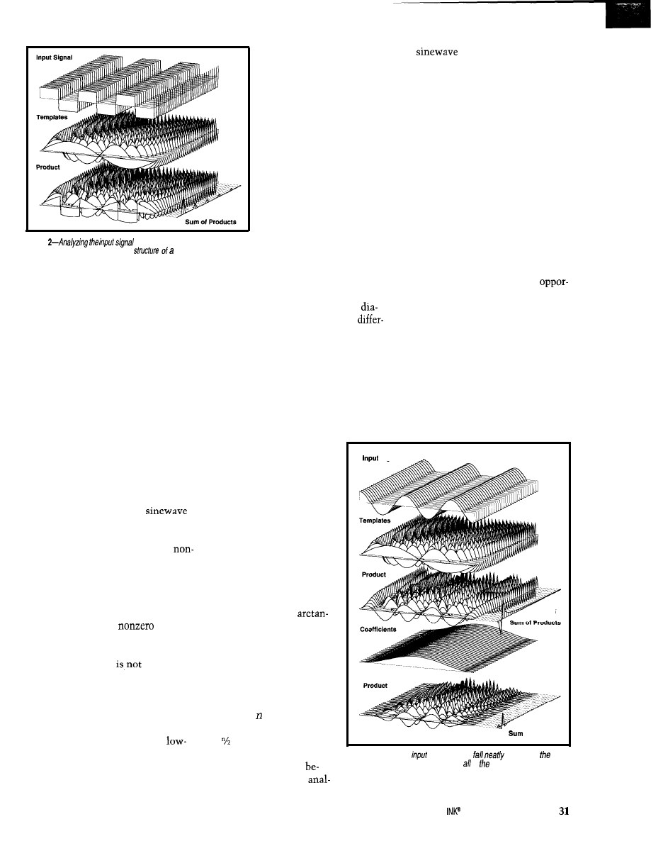
layers of Figure 2 illustrate this process.
The input signal in the top section
is the same for each frequency. The
center section shows the template
coefficients. You then
sum the results to get a
single number per trial.
In particular, the
cross-correlation
Figure la
the
and
waveforms
gives waveform in trace
d
get same wave-
form by adding
and
I
30
Issue
84 July 1997
Circuit Cellar
Figure
for various frequencies clear/y
shows the characteristic harmonic
square wave.
frequencies, with the lowest one in
front. The bottom section is the result
of point-by-point multiplication of
these two sections.
Integrating a continuous signal, or
adding up the samples of discrete sig-
nal samples, is one form of low-pass
filter-although not a real good one for
this application. So, the graph to the
right of the bottom section in Figure 2
shows the result of summing the results
from each trial.
input signal, B is the frequency analysis
template, and C is the FIR coefficient.
If you consider all the points in a
layer running front to back in the
gram, you can see that while B is
Now, let’s optimize it. If
you look at Figure 3 and
consider a single point in all
five layers, you see I’m doing
two multiplications in the
sequence A x B x C. A is the
The input signal is a square wave.
The graph clearly shows the decreasing
series of odd harmonics expected in
the spectrum of a square wave.
Figure 2’s input signal has frequency
components exactly matching the fre-
quencies used for analysis. However,
consider analyzing a single
with a frequency that doesn’t match
any template exactly.
Although there were plenty of
zero results after the multiplication
stage, most of them canceled out in
the integration stage.
In Figure 3, none of the trials have
results that cancel exactly. So, all the
frequency bins show
values
after integration.
Note that the difference frequency
present in each trial
exactly DC
in any trial. Using straight integration
as a low-pass filter enables these differ-
ence frequencies to show up in each
output bin because its frequency re-
sponse drops off relatively slowly.
The solution: design a better
pass filter for after the multiplication
stage, using the FIR technique I men-
tioned before.
The bottom sections of
Figure 3 show the results.
The fourth section shows
the FIR coefficients for a
relatively steep low-pass
filter. The last one shows
the result of multiplying
this point-by-point with the
results in the third section
and the curve generated by
summing them.
ysis
(or cosine wave) with a
frequency greater than half the sample
rate. Again, Nyquist rules.
Also, if the signal being analyzed has
frequency components that don’t exact-
ly match the bin frequencies, the an-
swer is spread across several bins. You
can minimize this with proper filtering.
While the DFT shows whether en-
ergy is present at a particular frequency
during a sample window, there’s no
indication of when the energy started
and/or stopped. I need small sample
windows to get better time precision.
However, small windows, with a
small number of samples per window,
give a smaller number of frequency
ent for each layer, A and C are the same.
Why not multiply A x C once, and
multiply that result by the different B
values? As Figure 4 shows, the result is
the same.
We don’t have a Fourier Transform
quite yet. Remember the sine/cosine
analysis with the cross-correlation?
And, recall that the DC value
depends on the phase rela-
tionship?
particular frequency (bin), why run all
bins. They also give poorer resolution in
the calculations for all bins? Why not
just calculate for the bin you’re inter-
the frequency domain and more
ested in, and use the other CPU time
to try the calculation with different
sample windows shifted in time. This
tunity for noise to get in and obscure
idea brings us back to the cross-corre-
lation we started with.
the result.
If you’re just looking for energy at a
Signal
I deal with these issues
by running a second analy-
sis using cosine waves of
the various analysis fre-
quencies. Then, I combine
the two sets of results into
an overall magnitude value
by taking the square root of
the sum of the squares of
the individual results.
I can also get a phase
angle by taking the
gent of the ratio of the two
results frequency by fre-
quency. Now, that’s the
complete Discrete Fourier
Transform (DFT).
To summarize, the DFT
analyzes a signal repre-
sented by points in time.
The answer is in the form
of numbers representing
V
of Products
discrete frequency bins.
This result occurs
cause we can’t use an
Figure 3-When fhe
signal doesn’t
info one of
frequency bins, there is leakage info of other bins. This example
shows a worst-case condition. Adding a better low-pass filter improves
the situation tremendously.
Circuit Cellar
Issue 94 July 1997
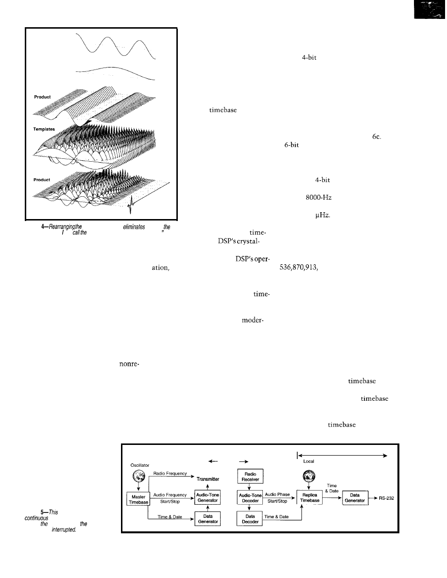
Input
Signal
Window
Sum of Products
a 32-bit DDS, I get a frequency resolu-
tion of 1.86
It also provides the data
for the modem signal that
gives the coarser measure-
ments of time (minutes,
hours, and date). I want my
receiver to become a replica
of this master timebase.
However, the receiver
already has a second
base-the
clock. It is divided down to
Figure
order of operations
much of
To give you a feel for what this kind
redundancy. Now, can low-pass filter a “window function.
of accuracy implies, I can set one such
DDS to the value 536870,912, causing
By the way, if you want to detect
controlled
it to generate a waveform at exactly
energy at a particular frequency and
drive various aspects of the
1000.00000000 Hz. I set another to
don’t care precisely when the energy
including the sample clock of the
making it generate
starts and stops, there’s an efficient
ADC that reads the radio receiver’s
1000.00000186 Hz.
form of the one-bin DFT known as
audio output.
After one day, the two generators
Goertzel’s algorithm. Analog Devices’
How can I replicate the master
differ by a phase angle of just 58”. It
ADSP-2101 app notes use this algorithm
base using the local crystal-controlled
takes nearly a week before they’re off
to build a DTMF decoder for telephone
timebase?
by a full cycle, providing the kind of
applications.
Let’s assume the crystal is
precision that enables me to account
The standard one-bin DFT calcula-
ately accurate, within 100 ppm (0.01%)
for the difference between the master
tion requires you to store the n samples,
of the frequency marked on its case.
and local crystal-controlled timebases.
multiply them by the values of the
Let’s also assume its exact frequency
If this seems a little confusing, take
template sine and cosine waves, and
doesn’t change significantly over time
a step back and consider a different
sum the results. This so-called
regardless of what it is.
point of view.
cursive implementation is analogous
A powerful and flexible approach of
As far as the DSP is concerned, it
to a finite-impulse-response (
FIR
) filter.
synthesizing any frequency from an
“thinks” that its local
is
Goertzel’s algorithm transforms this
arbitrary existing clock is called Direct
perfectly accurate and that I’m using
into the equivalent recursive form,
Digital Synthesis (DDS).
the DDS to track a distant
at
analogous to an infinite-impulse-re-
DDS is nothing more than a binary
a “wrong” frequency.
sponse (IIR) filter. The calculation then
register of some number of bits that
That’s fine for it, but you and I know
proceeds step-by-step as samples come
gets a number added to it at a steady,
that the remote
is perfectly
in, without storing them individually.
repeated rate (see Figure 6a). After a
accurate. The errors are in the local
This change significantly
decreases the amount of RAM
l
-
e
Reliable Output
required for each time the
Master
Unreliable
algorithm is used.
L i n k
Oscillator
Radio
E
l
Audio-Tone
Generator
DIGITAL SYNTHESIS
Now that we’ve nailed
down some techniques for
tone detection, I need to
deal with the fact that there
are two timebases. Figure 5
shows the entire system
from master oscillator to
receiver output.
One
is driven
by the master oscillator at
the transmitter. It controls
the starting, stopping, and
frequency of the audio tones
transmitted by the station.
few clocks, the register may overflow,
but you just keep going.
Figure 6b shows the results for a
simple
DDS circuit that’s clocked
at 16 Hz. The register numbers wrap
around at a rate proportional to the
number being added.
In fact, they give discrete samples of
a sawtooth wave whose frequency in
Hertz is the same as the number applied
to the adder.
Watch what happens as I add more
bits to the register, as in Figure
With
a
register, I can now specify S-bit
numbers representing O-8 Hz as before.
But, can I generate some fractional
frequencies between the ones I could
do with the
register?
This concept can be extended. If I
take my
sample clock and use
Figure
project should provide a
time and date signal even
though radio link from master clock
is frequently
3 2
Issue 84 July 1997
Circuit Cellar INK@
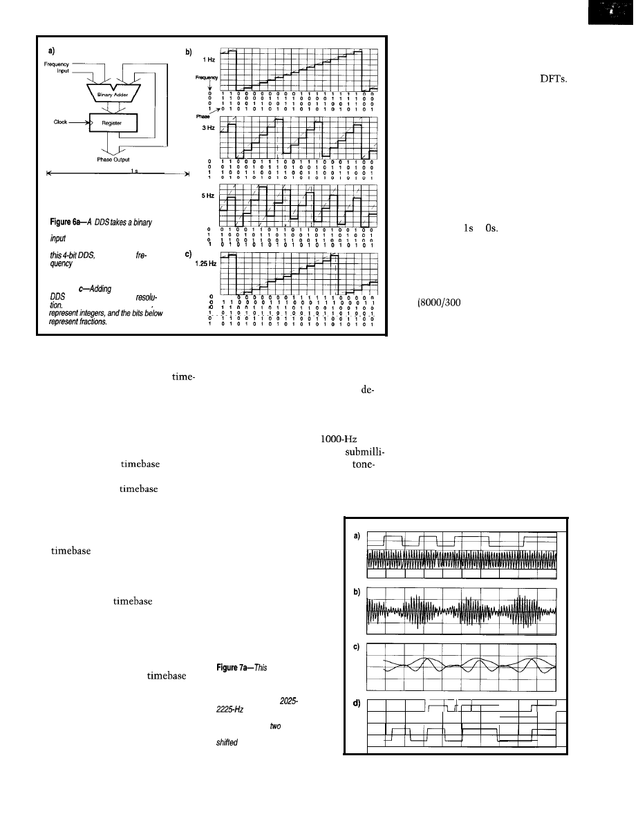
number representing frequency as
and produces a sequence of
numbers of phase as output. b-With
you see how
and phase are related. The
dashed lines show the continuous
functions of which the numbers are
samples.
more bits to a
improves its frequency
The bits above the dotted
line
timebase. Still, it doesn’t make any
There are two parts of the radio
difference to the algorithm.
signal in particular that 1’11 use in the
In any case, I use the replica
comparison between the master and
base as the basis for the ASCII output
replica timebases. First, I need to
of the decoder. Plus, I may later decide
code the 300-bps data to get coarse
I want other kinds of outputs that can
information like date, hour, minute
be derived from it.
and second.
When this window, which is used
for both tone detectors, is lined up on
a single bit worth of tone, one detector
output is at a maximum while the
other is at a minimum. Figure 7 shows
how this looks in real time.
I want to reduce these detector
outputs to two logical concepts. The
first is carrier detect, or whether either
of these tones is present at all, and the
Then, I’ll look at the
tone
FEEDBACK CLOSES THE LOOP
second is the actual data, or which of
bursts to line things up to the
the two tones is present. If I was just
So, now I have a
I can
second level. This is where the
building a stand-alone modem, these
adjust relative to the local crystal. But,
detection algorithms from Part 1 come
would become the CD (carrier detect)
into play.
and RXD (receive data) signals in the
RS-232 connector.
for each of those two frequencies,
using DDS to generate the local tem-
plate waveforms.
I use a sliding window for the
Since I’m doing only single bins, the
load on the CPU is no greater than an
FIR filter of similar size.
It also has the advantage of giving a
result for every input sample, provid-
ing the needed resolution in the time
domain.
I then compare the magnitudes of
the outputs of the detectors, using
their relative levels to pick out the bit
edges and decide whether the indi-
vidual bits are or
Each tone might exist for only one
bit time (at 300 bps at a time). To get
the maximum possible output from
the tone detectors, I use a window size
that’s as close as possible to the bit
size
= 26 samples).
how do I adjust the
so that it’s
a replica of the master timebase, espe-
cially given that the link from there to
here is rather unreliable?
The answer: feedback. After getting
the
going, I compare its out-
put (or portions of its output) to the
signal from the radio station. The re-
sults tell which way and how much to
adjust the replica
so that it is
synchronized.
In addition, I’ll assess the quality of
the radio signal so I know how much
to trust the results of the comparison.
If the signal is no good, I’ll ignore the
results and let the replica
free-run for a while.
It doesn’t matter what the local
crystal’s accuracy is. Only its stability
over time-or lack thereof-affects the
free-running accuracy of the replica
timebase.
SOFTWARE MODEM
The main task associ-
ated with decoding the
modem signal is recogniz-
ing the 2025 and 2225Hz
tones. My approach in-
volves setting up single-bin
DFT-style tone detectors
originaldata and
modem signal is created at the radio
transmitter. b--Notice the change after
noise and fading are added. c-These
outputs are from the
and
tone decoders. d-The upper
signal is the recovered data produced
by comparing the
signals in (c).
The lower signal is the original data
by ha/f the sample window
size.
1
I
34
Issue
64 July1997
Circuit Cellar INK@
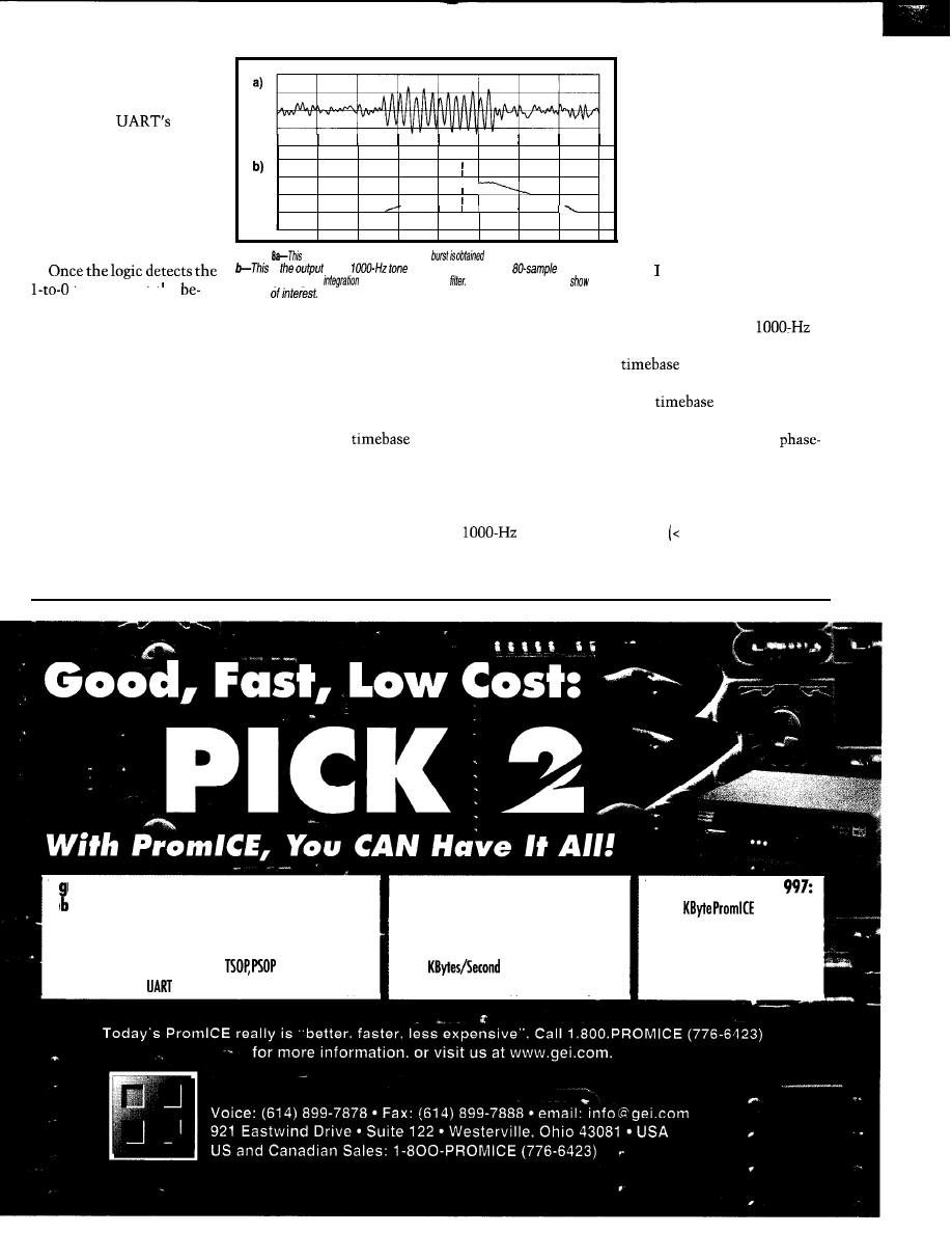
signals are established, I still
have to duplicate the func-
tionality of a
receive
portion to identify the start,
stop, and data bits. A hard-
ware UART normally works
by oversampling the data
using a free-running clock
that operates at 16 times the
expected data rate.
Figure
noisy, band-limitedtone
from the radio receiver.
Once these two logical
tone detector window for
better noise rejection.
Figure 8 shows the results
of such a tone decoder work-
ing on the noisy, band-limited
signal from the radio receiver.
I take the output signal from
this decoder and try to iden-
tify two moments, separated
by the window size, where
the difference is greatest.
is
of the
decoder, using an
window size
. . .
transition at tne
and using
straight
as the low-pass
The vertical markers
an
adjust the positioning of
interval
these moments by altering
the frequency of the DDS
that’s producing the replica
signal. Once that’s done, the rest of the
replica
can be derived from
this DDS.
ginning of the start bit, it
uses the clock to predict where the
bits’ centers are going to be and checks
the value of the data line at those in-
stants in time. A shift register captures
the data bits and presents them to the
CPU in parallel form.
difference to the operation of these
tone decoders.
ULTIMATE ACCURACY
I mentioned I’d use DDS to generate
the sine and cosine waves at 2025 and
2225 Hz mainly because it’s an easy
way to get these frequencies. It doesn’t
really matter whether these DDS gen-
erators are frequency-locked to the
master timebase. The difference of a
few 10s of ppm doesn’t make any real
Identifying the bit edges and decod-
ing the data enables me to set the
replica
to within -10 ms of
the master timebase.
I should be able to get the accuracy
to another order of magnitude (1 ms)
by carefully searching for the leading
and trailing edges of the
tone
bursts. Since these bursts exist for a
minimum of 10 ms, I can use a longer
Once the
is set to within
one cycle at 1000 Hz (1 ms), the final
refinement would be to use the
angle measurements that we get from
the tone decoder.
This change could theoretically get
the accuracy down to a fraction of our
sample period 100 us). However, the
short-term radio path length variations
may make this a moot point.
Hi h performance memory emulation and
de ugging:
l
Stable and reliable on today’s embedded systems.
l
New faster access speeds now standard.
l
The best connection solutions for
and PLCC chips.
l
Expanded Virtual
support for industry-standard debuggers.
Ultra-Fast code downloads reduce
development time:
l
New high-speed download support for
Windows NT
l
90
over a PC parallel port.
l
low-cost Ethernet support for UNIX systems.
New lower Prices for 1
l
128
now
just $495.
l
Source-level debugging systems
at a fraction of an ICE’s cost.
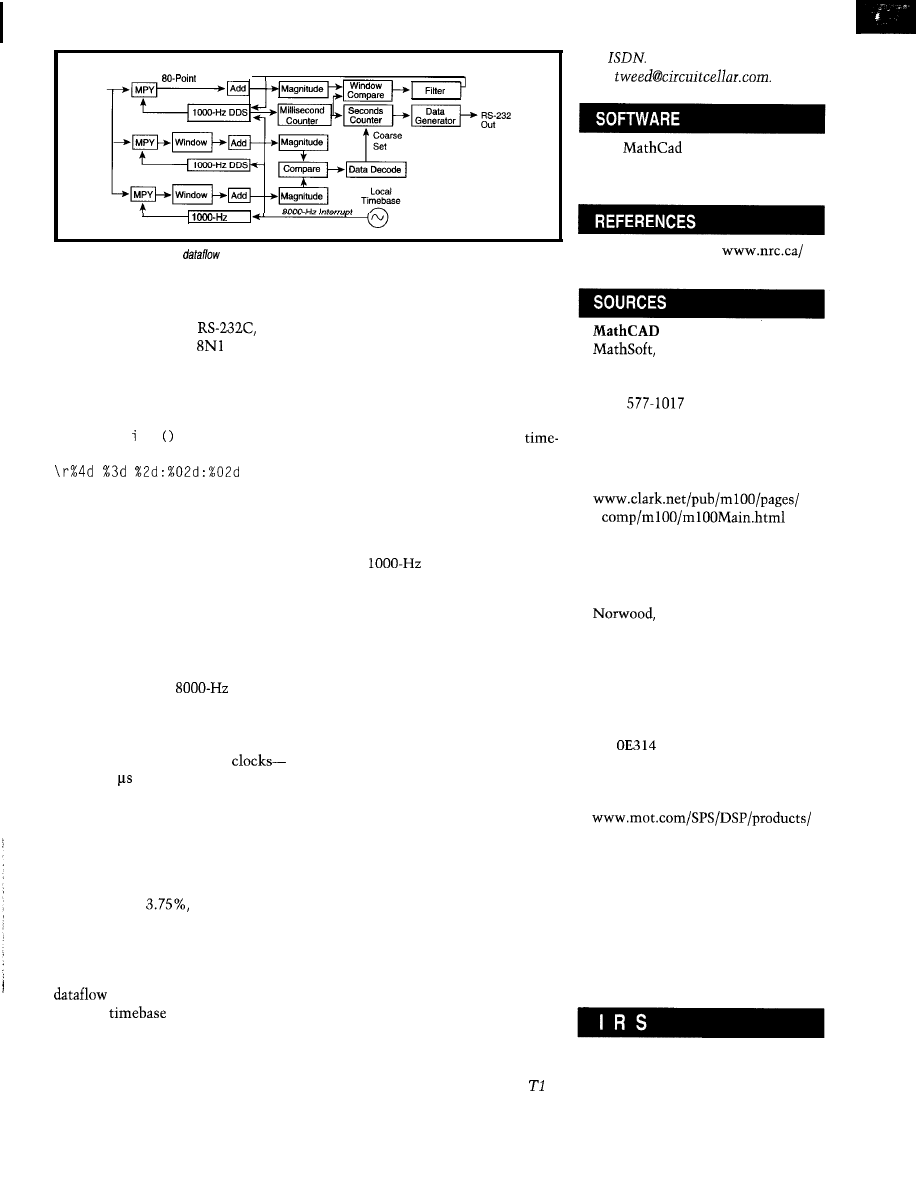
Audio In
DFT
Fine Adjustment
DDS
Figure 9-The final sofhvare
diagram shows the details of selected algorithms.
GENERATING THE OUTPUT
Remember, the receiver’s output
signal was specified as
using
ASCII characters in an
configura-
tion. The data rate was left unspecified,
except to say that it will be between
300 and 9600 bps.
The output string is in the form
(using C p r
n t f
notation):
The CHU receiver isn’t quite com-
plete. In this series, I wanted to make
clear through the extensive use of
graphics some of the theory and imple-
mentation issues behind some com-
mon DSP techniques.
This project is a basic CHU receiver
that emits a simple time and date
signal that’s locked to the master
base at the transmitter. It could be
enhanced by:
where the individual fields are year,
day of year, hours, minutes, and sec-
onds UTC, using 24-hour notation.
I also stated that the string would be
transmitted so that the last character
ended just as the named second began.
Using a bit-rate generator tied directly
to the replica time (i.e., another DDS)
would be an easy way to accomplish
this. It would be just another small
task running at the
sample
rate of the rest of the system.
However, with this approach, the
bit edges in the output signal can only
occur exactly on the sample
every 125 or multiples thereof. If I
want to use standard computer data
rates like 9600 bps, timing jitter at the
bit edges distorts the bit widths.
l
adding an automatic gain control to
help correct for the effects of fading.
It could be keyed on the amplitude
of the
tone bursts in much
the same way that a TV receiver
keys on the sync tips.
l
using a remotely-controllable radio
receiver and scanning all three radio
frequencies to select the best signal
l
making the RS-232 output format
configurable for different applica-
tions. This would include making
more of the data available in the
output (e.g., UT1 for astronomers).
l
generating one or more continuous
audio frequency reference outputs
from the DDS via the DAC
Lower data rates minimize this
distortion in terms of a percentage of
the bit width. At 300 bps, the distor-
tion is at most
which should be
acceptable to any computer SIO port.
And, if you build your own radio
receiver, you can use RF carrier fre-
quency and phase measurements.
I’m interested in any enhancements
you might think of, so feel free to
contact me.
q
PROJECT ENHANCEMENTS
Figure 9 shows the detailed software
Dave Tweed has been developing real-
diagram with the tone detec-
time software for microprocessors for
tion and
filled in. You can see
more than 18 years, starting with the
that the initial architecture wasn’t far
8008 in 1976. He currently designs
off. Now, it’s specific enough for me to
equipment for carrying high-quality
start thinking about implementation
audio and wide-bandwidth data over
details.
digital telephone services such as
and
You may reach him at
dave.
The
documents I used to
generate graphics for this article are
on the Circuit Cellar Web site.
Radio station CHU,
inms/whatime.html.
Inc.
101 Main St.
Cambridge, MA 02142-1521
(617)
Fax: (617) 577-8829
www.mathsoft.com
TRS-80 Model 100
Andy Diller’s Web 100 Main Page
ADSP-2101, ADSP-2181, EZ-Lab,
EZ-Lab Lite
Analog Devices
One Technology Way
MA 02062-9 106
(617) 329-4700
Fax: (617) 329-1241
www.analog.com
DSP56000
Motorola
6501 William Cannon Dr. W
MS
Austin, TX 78735-8598
(512) 891-2030
Fax: (512) 891-3877
TMS320
TMS320 series
Texas Instruments, Inc.
34 Forest St.
MS 14-01
Attleboro, MA 02703
(508) 699-5269
Fax: (508) 699-5200
www.ti.com
407 Very Useful
408 Moderately Useful
409 Not Useful
36
Issue 84 July 1997
Circuit Cellar INK@
DSP COPROCESSOR BOARD
The SPIRIT-32 is a low-cost, high-perfor-
mance,
PC/l
04-form-factor DSP module based on
the Texas Instruments
DSP. With up to
four channels of A/D and D/A, it’s ideal for use with
The SPIRIT-32 features a 32-bit floating-point processor with
a
or
performance rating, two banks of
internal 256 x 32 zero-wait-state SRAM, 64
x
32 cache, flash
memory, and an RS-232 interface off the main memory bus. offers
all the functionality of
DSP devices (e.g., a program debugging
interface via the MPSD emulator port). As well, the chip’s timers,
interrupts, and software-controllable I/O flag lines are brought out
to a processor expansion connector (PEC) on the module.
The suite of development tools for the SPIRIT-32 includes
RadiSys’s Brahma MPSD emulator/debugger, an RS-232 library
for application development, and
PC-based Run Time
Library for DOS, Windows 95, or Windows NT, as well as Tl’s
optimizing C compiler/assembler/linker for the C32. A DSP
function library for the C32 DSP is also provided.
The
SPIRIT-32 with standard 32 K x 32 SRAM sells for
$795 in
quantities.
Corp.
5445 NE Dawson Creek Dr.
Hillsboro, OR 97124
(503) 615-1100
Fax: (503) 615-l 150
www.radisys.com
SINGLE-BOARD COMPUTER
The
is a single
board computer designed for
rugged, mobile, embedded
transportation applications. The
board is builtaround theSMX/
386
single-de
vice PC (SDPC) that includes a
CPU, core
logic, a DRAM controller, and
or
ISA busing. It also
has serial and parallel I/O
ports, floppy and IDE disk con-
trollers, an
BIOS,
an embedded version of DOS,
and 256 KB of flash memory.
The
integrates the
seven
serial ports, two
ports,
2.2 MB of flash memory config-
ured as a solid-state disk, and
support for up to 15 MB of
additional external removable
disk storage. The board is de-
signed to cope with vibration,
electrical noise, and power fluc-
tuations.
The
includes mul-
tiple industry-standard inter-
faces to maximize design flex-
ibility. The full 16-bit ISA bus
(accessible through a PC/l 04
connector) enables
with a wide choice of
modules. An SAE 1708 serial
interface for communications
between microcomputer sys-
tems in heavy-duty vehicle ap
is included, as is a
port for connection of a GPS.
T h e
sells for
$731 in quantity.
ZF
Inc.
1052
Ct.
Palo Alto, CA 94303
(4 15) 965-3800
Fax: (415) 965-4050
INK JULY 1997
GRAPHICS CONTROLLER
The
expansion module is a highly
versatile flat-panel and
play controller that can inter-
face PC/l
em-
bedded systems to color and
monochrome LCD panels, color
and monochrome electrolumi-
nescent (EL) displays, and ana-
log CRTs. Simultaneous display
output on both a CRT and a flat
panel is also supported. Full
software compatibility with five
popular video
VGA, EGA, CGA,
and
easy sys-
tem development and support
in a broad range of embedded
applications.
The module supports resolu-
tions of up to
1280 x 1024
in 16 colors, as
well as 24-bit
true color in
6 4 0 x 4 8 0
resolution. In
addition, the
display con-
troller includes
a GUI accel-
erator that can
crease the per-
formance of
Windows and many other
graphic-intensive applications.
A number of features to facili-
tate the incorporation of
panel displays into embedded
applications are included. A pro
grammable VGA BIOS in
flash memory supports
the diverse signal timing and
interface requirements of differ-
ent flat-panel technologies and
manufacturers. A variety of pro
grammable display centering
and stretching functions allows
the use of displays whose reso-
lutions exceed that of the soft-
ware in use. Power manage
ment and sequencing functions
are included to control the use of
system power by the flat panel
and to prevent damage to LCD
panels during system power-up
and powerdown. Software-pro
grammable grayscaling,
rate control, and dithering func-
color simulation on
.
monochrome displays.
The
II sells for $299 in quantity.
A
development kit
for first-
time purchasers, which comes
with a comprehensive techni-
cal manual and software utili-
ties, is available for $416.
Computers
990
Ave.
Sunnyvale, CA 94086
(408) 522-2 100
Fax: (408)
1305
PC/l 04 RESOURCE
GUIDE
The PC/l 04 Consortium
announces the tenth edition of
its PC/ I 04
Resource Guide.
The
free
book is
also available on CD-ROM. In
addition to overviewing the
PC/l 04 standard, this year’s
edition details PC/l 04’s PCI
equivalent, PC/l
To order, call or fax the
PC/l 04 Consortium at:
(415) 903-8304
Fax: (415) 967-0995
LOW-VOLTAGE EPROM EMULATOR
Scanlon Design has introduced two low-voltage EPROM emulators. The
El LV-90
and
enable operation at 3.3 and 5 V, respectively, and emulate EPROMs up to 1
(El) and 4 Mb (E4). RAM and flash memory are also supported. Both emulators offer
error checking and correction while downloading and draw a maximum of
5
The emulators include software that permits live editing of the
emulation memory.
These compact emulators are completely software configurable
with an integrated memory back-up circuit. Each comes
plete with
and 32-pin DIP adapters, and 32-pin PLCC
adapters are available. Fast access time (30 ns) models
are also available.
The emulators retail from $229.
Scanlon Design, Inc.
5224 Blowers St.
Halifax, NS
l
Canada
(902) 425-3938
Fax: (902) 425-4098
REMOTE SOFTWARE DEBUG
W ’ d
Remote Debugger
is a
ows-hosted GUI source-level debugger for
embedded-system software development. A Remote
Debugger enables an embedded application to be
loaded from the host PC and debugged on the target system.
Program execution on the target system is controlled by the
Target Monitor, which communicates with the host via an RS-232
serial port.
has a number of
target
monitors, and
enable the user to build a custom target monitor.
provides source-level and symbolic debugging for C
and mangled C++. It also provides various windows to show code
in source, disassembler, or mixed views, as well as define
breakpoints based on symbolic address, expressions, and debug
register expressions. These windows view memory in various
formats, evaluate and view C expressions, and show active chain
of function calls and active local variables. They also let the user
read and write any I/O port, as well as view and edit symbols.
may be hosted on systems running Windows 95,
NT, or 3.x. The software is supported by
absolute linker/
loader and Link&Locate ‘386. It accepts files in the Intel
bootloadable formats along with the binary image
formats.
Remote Debugger sells for $1795.
Systems Software, Inc.
18012
Cowan, Ste.
100
Irvine, CA
926 14
(714) 833-1700
l
Fax:
(714) 833-1900
www.ssi.com
SHARC DSP MODULE
Research’s
is a powerful floating-point DSP module in a
form
factor. Based on the Analog Devices SHARC DSP, it offers
processing resources.
Silvertip’s PC/l 04 bus interface gives host computers direct
access to the
40-MHz SHARC processor’s
IOP registers and DMA-driven host port.
The host can reset and boot the SHARC, load program images, and examine memory.
Silvertip can operate with a PC/l 04 host or in stand-alone mode using its
boot
flash. The board’s minibus expansion connector extends a portion of the SHARC
processor bus to additional I/O or memory devices via 22 address and 32 data lines,
plus two interrupt inputs, two serial ports, and a SHARC link port.
Silvertip is supported by sourcecode development tools including Analog
Devices’ SHARC ANSI-compliant C compiler assembler, linker, simulator, and
source-code debugger. True real-time in-circuit emulation is available with the
optional EZ-ICE emulator.
DSP2 1
host
I/O and DSP functions, sample code, and diagnostic utilities under DOS and
Windows 3.1, 95, and NT.
List price for an ADSP-2
Silvertip is
$1695.
An ADSP-2
version is available for $2495.
Research Systems
33 N. Main St.
Concord, NH 03301
(603) 226-0404
Fax: (603) 226-6667
www.bittware.com
40
INK JULY 1997
Ethernet
Adding Ethernet to an embedded design gives you
via he Internet.
Chip brings together an embedded Ethernet platform and
an
Am
86. He gives
guidelines for layout, chip clocking,
storage, as we// us
concerns.
ith the explosion of the Internet, the
need for embedded Ethernet connectivity is
becoming more common.
Ethernet networking provides a conve-
nient, standardized means of connecting
diverse systems-from software development
tools, to point-of-sale systems, to the much
anticipated “smart house.” It’s also widely
used to interconnectsubsystem components
in larger designs.
In this article, I explain how to design a
simple,
standalone Ethernet plat-
form using the
86 family of micro
controllers with the
Media
Access Controller for Ethernet (MACE).
Using the microcontroller’s features, this
platform can be the brains of a variety of
embedded devices. Ifyourembedded appli-
cation already uses a ‘186, you’ll see how
Ethernet can easily
be added
to
your design.
Of course, the hardware is just the start
of the solution. The popularity of Ethernet
as a system-connectivity solution lies in the
universal acceptance of the Internet Proto-
col (IP) standard.
Compliant Ethernet devices rely on the
services of IP, TCP, UDP, and other
understood and readily available proto-
cols. So, also discuss software issues such
as device drivers and protocol stacks.
H A R D W A R E C O N N E C T I O N
Figure
1
diagrams a complete Ethernet
solution for an embedded microcontroller
application as well as the interface be
the
86ES and the MACE.
The Am
is a high-performance
‘x86 microcontroller available in
speed grades. The integrated
peripherals and
interface to
memory make it an ideal solution for many
embedded devices.
The MACE is a highly integrated
type Ethernet controller incorporating the
logical MAC and PHY layer (Manchester
encoder/decoder and 1 OBaseT transceiver).
The
interface makes connection to a
‘x86-style Local bus straightforward.
The microcontroller section consists of
the
flash, and SRAM.
ration includes
flash memory and
SRAM,
but
of course, exact memory
size varies by application.
Some designs eliminate the flash and
download the microcontroller’scodedirectly
into SRAM. This task is accomplished by
asserting HOLD or RESET to the processor to
gain control of the processor’s memory bus.
A typical general-purpose
stack
requires about 48 KB of code and 48 KB of
data memory. So, most embedded Ethernet
applications can fit in 128 KB of total
memory space.
The Ethernet section consists of a PAL for
glue logic and the
MACE. The
design relies on the Am
integrated
DMA channels for high-performance data
movement between the MACE and the
microcontroller’s memory.
Support circuitry not shown (e.g., the
RS-232 interface, Ethernet isolation trans-
formers, and
connector for 1 OBaseT) is
covered in app notes available from AMD.
Also not shown is the rest of the applica-
tion-the embedded target design itself.
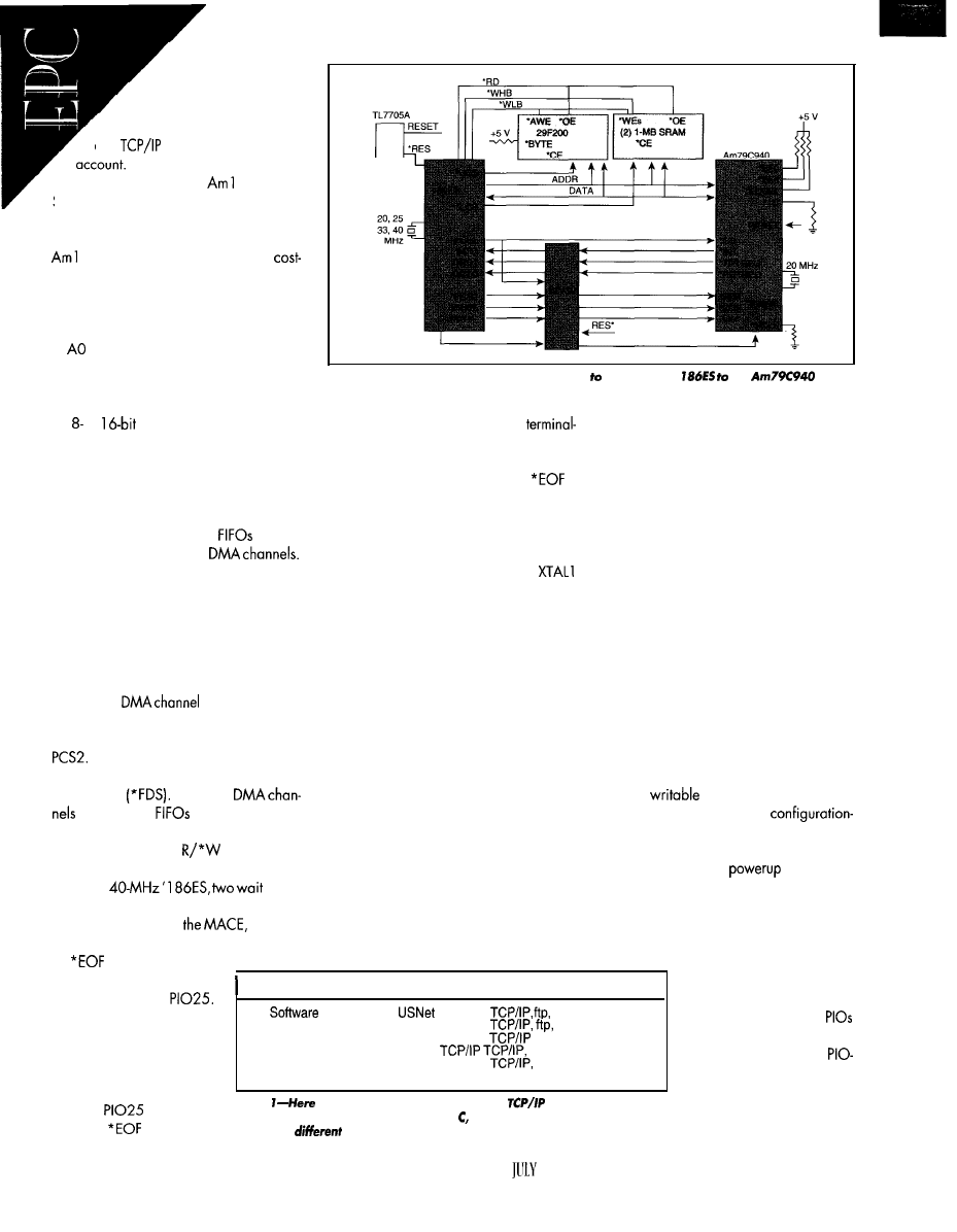
Just keep in mind
that the microcontroller
performs other duties as well.
Their interaction with the Ethernet
and
tasks must be taken into
My design uses the
86ES with
SRAM, which is a good combination when
RAM requirements are small. But, if your
RAM requirements exceed 128 KB, the
86ED plus DRAM is a more
effective solution.
DESIGN OBSERVATIONS
Al of the microcontroller bus connects
to
on the MACE processor interface.
Thus, all accesses to the MACE’s internal
8-bit registers are on even addresses. From
the microcontroller’s perspective, they can
be or
accesses.
Figure
I-This simplified diagram shows how connect a Am
the
MACE.
The least significant byte of such ac-
cesses contains the valid 8-bit data. The
most significant byte can be ignored. The
MACE register chip select (*CS) connects
to *PCS3 on the microcontroller.
After the DMA channel starts and the
MACE begins transmitting, a DMA
count interrupt occurs. In this event’s ISR,
PI025 is set to 1 and the DMA channel is
set to transfer one more word.
is
active during this transfer, and the MACE
recognizes the end of the transmit packet.
The PAL equations in Listing 1 contain a
state machine that resolves a MACE receive
EOF issue. After the processor DMA reads
the last word from the MACE’s receive
FIFO, the MACE doesn’t deassert RDTREQ
for up to four cycles-long enough to
inadvertently latch one more DMA request.
Accesses to the MACE’s
are ac-
complished via the ‘186ES
One channel is responsible for transmitting
data, and the other for receiving data.
This design uses two separate clock
sources-one for the microcontroller and
the 20-MHz source for the MACE
and XTAL2 inputs.
Both DMA channels should address
PCS2. For receive operation, DMA chan-
nel 0 should have its
source address set to
PCS2 and its destination address set to the
software-supplied buffer memory address.
Fortransmit,
1 should have its
source address set to the supplied buffer
memory address and its destination set to
If your design deviates from this ar-
rangement, ensure that you still meet the
stringent requirements for an external clock
source for the MACE. Improper Ethernet
chip clocking can be a major source of
equipment incompatibility and is often dif-
ficult to track down as the cause of equip
ment malfunction.
If this DMA transfer is allowed to occur,
the first of the receive status bytes will be
read and placed into the DMA buffer.
Software must then be aware of and re-
cover from this event.
However, the PAL state-machine inter-
cepts RDTREQ and disallows DRQO for
seven cycles after the receive EOF. This
feature prevents inadvertent DMA cycles,
eliminating the need for a software
workaround.
*PCS2 connects to the MACE’s FIFO
Data Strobe
Thus, both
address the
on the MACE. As
you see in Listing 1, a term in the PAL
equations ensures that
on the MACE
is driven correctly during these accesses.
The *EAD/R pin is tied low as per its
description in the MACE manual. This as-
sumes that the external address matching
feature is not used.
NONVOLATILE STORAGE
With a
states
must be inserted for PCS2 and PCS3 cycles.
*TC is pulled down on
resulting
in three-cycle MACE timing
Associated register bits must be correctly
set by software. This includes the Match/
Reject bit in the Receive Control Register,
which should be left at its default. This
configuration allows internal address match-
ing (or promiscuous mode) to override the
external address detection.
Many Ethernet applications require some
type of
nonvolatile memory, usu-
ally for IP addresses or other
specific set-up information. Accesses to
nonvolatile memoryarelypically infrequent,
being done mostly at
or when the
end user changes the configuration.
EEPROM is a popular method for stor-
ing such data. Parallel EEPROMs can be
connected to the address and data bus and
is supplied, to the
MACE during writes, accord-
ing to the setting of
For transmit operations, the
MACE device driver should
set the transfer counter for
the write DMA channel to 1
less than the numberofwords
to write.
is set to 0,
meaning
is inactive.
Vendor
Product
Protocols Supported
US
EBS, Inc.
telnet, ping,SNMP
RT-IP
telnet, PPP
Accelerated Technology
Nucleus Net
Pacific Sottworks
Fusion
SNMP, PPP, SMTP
XLNT
Stackware
Integrated Systems
Attache +
UDP, telnet, ping
IP, UDP, TCP
Table
is a list of the more well-known
protocol stack
vendors. These stacks are available in and all offer excellent support for
porting to
targets.
44
CIRCUIT CELLAR INK
1997
driven with one of the avail-
able chip selects.
For serial EEPROMs, it’s
relatively
easy to use the
to implement a serial inter-
face. A driver for such a
style serial interface is simple
to write.
Of course, nonvolatile
data can also be stored in
Hook your target to
a simple network consist-
ing of a UNIX or PC host, a
hub, and
a
Then, ping your target at the
appropriate address.
If you don’t get a reply, double check the
networkconfiguration.Makesureyourdriver
code is configuring the MACE correctly. Pay
special attention to the address configura-
tion since it’s a common cause of problems.
Next, see if the MACE is asserting
RDTREQ. If so, then it’s receiving data and
flash. This technique has the advantage of
not requiring another device, which can
help keep costs down. Software is then
required to manage the task of writing the
saved data to the flash device.
BOARD LAYOUT
Once the design is on paper and you’re
ready to lay out the board, take time to
learn about the recommended layout prac-
tices for Ethernet designs (see References).
In a nutshell, Ethernet interface devices
contain both analog and digital circuitry.
Typically, a device’s analog portions are
confined to an isolated part of the chip,
which helps reduce digitally induced noise
on the sensitive Ethernet-analog physical
interface.
On the PCB, it’s common practice to
provide isolated analog power and ground
planes. Separate powersupplydecoupling
for
the
analog section is also recommended.
AND DEBUG
When boards return from assembly,
take a few common-sense steps to verify
that your Ethernet design works properly.
First, get the microcontroller section run-
ning correctly. It should be fetching instruc-
tions from flash and correctly accessing
SRAM.
Most designs use a monitor to aid in
development. Typically, this monitor uses
oneoftheserial
and provides a user interface that can be
displayed using an ANSI terminal or emu-
lation program (e.g., Hyperterm).
Once the monitor is booting from flash
and running properly, it’s time to check out
the Ethernet section. The design in Figure 1
has the MACE’s register interface on Pe-
ripheral Chip Select 3.
Aftercorrectlyconfiguring
86ES
PACS (offset
and MPCS (offset
for proper operation, you can try to read the
MACE registers. Usually, the
86ES
registers are configured to place the MACE
in I/O space at 300h.
If you’re using this configuration, per-
forming an I/O read at 320h using the
monitor’s I N command returns thecontents
of the MACE chip-ID LSB register. It should
be a 40h.
An I/O read from 322h should return
x9, where x is dependent on the MACE
version. Then, check out MACE writes by
writing to a MACE read/write register and
reading it back.
If you get these results correctly, it’s time
to get your MACE driver software working.
After porting, the best testing method is to
link a simple test application that includes
the driver,
stack, and ping applica-
tion.
Usually, the ma
i n
program can do
nothing more than initialize the stack and
hardware interface and then just wait. As
part of porting the stack and driver, you
have to supply a unique Ethernet 802.3
MAC address, an IP address, and possibly
a name domain address.
Developing real-time embedded applications doesn’t have to be
time consuming difficult-you just need to have the right tools.
Paradigm alone
has the high performance development tools you
need to streamline the embedded system software development
process so your Intel and
applications are ready in record
time. Paradigm’s complete suite of tools work with industry standard
C/C++ compilers from Borland and Microsoft, as well as hardware
development tools from Applied Microsystems, Beacon Development
Tools and other popular in-circuit emulator vendors.
Call at 800-537-5043 today and let take care of all your
development tool needs, so you can keep your focus where
you need it-on your application.
troller to DMA it to memory.
After verifying that DMA
IS
configured and operating cor-
rectly, check that the MACE is
naling the end of packet
by
asserting the
interrupt to the
86ES. If everything is
happening correctly, begin debugging any
software problems you might have.
By working upwards from the lowest
levels of the hardware into the software,
you can systematically find and eliminate
problems.
By the time you’re done, you should be
getting responses to your ping requests.
Setting breakpoints or debug messages in
your ping application code verifies
that
your
stack is working properly.
It’s then time to try an or other
intensive test. Once it works correctly, you
can proclaim the Ethernet section opera-
tional and move on to integrating the
Ethernet with your embedded application.
You aren’t quite done with the hardware,
but the software tasks can now proceed. To
be truly finished with the hardware, your
Ethernet interface must
802.3 specs.
S O F T W A R E C O N S I D E R A T I O N S
In addition to application software, an
embedded Ethernet design requires at least
Ethernet drivers, almost always a network
protocol stack, and probably a real-time
operating system.
Choosing a protocol stack is a matter of
matching design requirements and budget
to available sources. Freeware stacks re-
duce initial costs, but they can take a lot of
time to install correctly and may suffer from
terrible performance.
At the other end of the spectrum, ven-
dors such as Integrated Systems offer a wide
range of high-level protocols (e.g., RMON)
as well as porting and integration services
(see Table 1). High-end stacks may cost
more, but they’re worth it if performance
and time-to-market are critical.
All commercial protocol stacks have a
few targetdependent modules that provide
independence from hardware drivers and
RTOS
To interface to a new hardware
driver or RTOS, only these interface mod-
ules need to be changed so that generic
calls(e.g.,send_packetortask_wait)
are replaced by the calls specific to the
given driver and RTOS.
Therefore, you can use pretty much any
protocol stack with any combination of
46
hardware drivers and RTOS. Most stacks
also come with drivers for the most com-
mon Ethernet chips and interface modules
for the most popular
A base set typically includes basic pro
and applications like IP, UDP, ping,
and telnet. You pay extra for extensions like
TCP, ftp, PPP, SNMP, RMON, and other
higher level protocols and applications.
There are also shareware and freeware
available. One system, Packet
Driver, is not a
stack itself, but if you
unzipthefileandlookatsoftware.doc,
you find a list of various protocol stacks
(including several
packages) and
other applications supporting Packet Driver.
Some are suitable for embedded applica-
tions.
N E T W O R K C O N T R O L
The design presented here is just a
starting point. Adding Ethernet to an em-
bedded design opens a whole new world
of possibilities for the target system.
A recent AMD project included a port of
US Software’s
stack. After we
ported the
stack, engineers at US
Software loaned us a copy of their recently
developed
server application.
We ported it to our demo board and
wrote an HTML page to enable a Web
browser to change the state of the micro’s
programmable I/O pins. We also wrote a
CGI script for the board to return an HTML
page showing the current state of the
On this 3” x 3” demo board, the
being controlled are connected to
Listing I-These PAL Equations
the Am
design are
in
for a
Declaration
TITLE
to MACE Glue Logic
DEVICE
PLCC
2 clka
PIN Declarations
from 186EM
PIN 3
chip select from
DMA to/from MACE
PIN 4
chip select from
regular cs to/from MACE
PIN 5
from
used to drive EOF on DMA writes
PIN 6
data direction from
used to generate
PIN 7
receive DMA request from MACE
PIN 9
transmit DMA request from MACE
PIN 10
interrupt request from MACE
PIN 11 reset_
reset, for state machine
PIN 17
state machine term
PIN 18 Xl
state machine term
PIN 19 X2
state machine term
PIN 20
interrupt request to 186ES
PIN 21
receive DMA request to
PIN 23 drql
transmit DMA request to 186ES
PIN 24
FIFO data strobe for MACE
PIN 25
EOF for MACE
PIN 26
read/write for MACE
PIN 27
for MACE
EQUATIONS
Boolean Equation Segment
=
invert interrupt pin
drql =
invert transmit dma request
=
MACE FIFO data strobe is
=
build
from chip selects and
=
;eof follows sense of
when enabled
=
*
enable EOF as output on FIFO writes
sclk.clkf = clka
:=
divide 186 clock by 2 to get
clock for MACE
=
*
allow DMA
req only in state 0
XO.CLKF = CLK
use clka as the master clock for registered
= CLK
outputs
= CLK
Downcounter state machine idles in state 0. When set to state 7,
it counts down on each clock to state 0. The disable state machine
gets set to state 7 when receive EOF occurs.
to the
is allowed only in state 0.
GLOBAL.RSTF = RESET
reset configures to state zero
GLOBAL.SETF =
receive EOF sets it to state 7
:=
* * x2 +
* /Xl * x2 +
* Xl *
Xl := * x2 +
* /Xl * x2 * * /x2
x2 := * Xl * x2 +
* Xl * x2 + *
* x2
CELLAR INK JULY 1997
So, any user with
and the right
toggle the board’s
the
world’s fanciest blinking-light demo!
While this exercise might seem silly, it
clearly shows how to provide a Web front
end for any embedded application. Once
you can control a PIO, you can control
anything.
Chip
is a
marketing
engineer in
embedded-processorgroup, special-
izing in networking
and
telecommunications
applications. Previously, Chip was a soft-
ware
engineer
W
where he
worked on 5250 terminal emulation and
high-speedpageprinteremulationproducts
for IO years. You may
reach him at chip.
For o list of shareware/freeware
see
For freeware
protocol stacks, download
from
REFERENCES
Texts
AMD,
“Embedded Network Applications De
sign Guide
Kit,” PID
1996.
AMD,
Media Access Controller
for Ethernet,” PID
1994.
M.A. Miller,
M&T Books, Red-
wood City, CA, 199 1.
W.R. Stevens,
Addison-Wesley
Publishing, Reading, MA, 1994.
Internet
html
comp.arch.embedded
comp.protocols.tcp-ip
SOURCES
Am 186 controllers,
MACE
Micro Devices, Inc.
One AMD PI.
Sunnyvale, CA 94088
(408) 732-2400
www.amd.com
US Software Corp.
142 15 NW Science Park Dr.
Portlond, OR 97229
(503) 64 l-8446
Fax: (503) 6462413
RT-IP
Inc.
P.O. Box 873
Groton, MA 0 1450
(508) 448-9340
Fax: (508) 448-6376
www.etcbin.com
Nucleus Net
Inc.
P.O. Box 850245
.
Mobile, AL 36625
.
(205) 66 l-5770
.
Fax: (205) 6615788
Fusion
Pacific Softworks
4000 Via Pescador
Camarillo, CA 93012
(805) 484-2
128
Fax:
(805) 484-3929
Stackware
XLNT Designs
15050 Avenue of Science
San Diego, CA 92 128
(619) 487-9320
Fox: (6 19) 487-9768
Attache+
Integrated Systems
201 Moffett Park Dr.
Sunnyvale, CA 94089
(408) 542-l 500
Fax: (408) 542-l 961
4 10 Very Useful
4 1 1 Moderately Useful
4
12 Not Useful
NEW!
“A
f o c u s e d b o o k t h a t
delivers what it promises: detailed
technical information on the parallel
port.”
Windows Developer’s Journal
“It’s
been a while since I’ve seen a
book as practical as this one.”
Volts
ISBN O-9650819-1-5
$39.95
343
pages
Includes disk
“An ideal introduction to low-end
embedded design.” EDN
“The writing is a model of
and conciseness.“-
ISBN 0-9650819-O-7
273
pages.
$31.95
Order Ii ne: l-800-247-6553
more information or international orders:
Research Phone
Shipping:
$5.00
Winnebago St.
53704
6 0 8 - 2 4 1 - 5 8 4 8
JULY
Just
connect a keyboard,
adiskdrive
md your ready to run. Or
brget the drive and boot
from a Flash disk.
Modules for
%x/Modem, SCSI, Ethernet,
I/O,
and PCMCIA.
for Point Of Sale and
Prices start at $200.00
1.
CPU Selection:
DX2,
All
have Real Time Clock, Serial, Parallel, IDE, and Floppy.
On Board Watchdog Timer.
BIOS with Power Saving Green Mode.
Wide Bus Selection: PC/ 104. ISA, PCI.
10.4”
super bright LCD Panel Kits.
Hardware and Cable kits included for most boards.
Fax 457-0110 BBS 529-5708
11 EMAC WAY, CARBONDALE, IL 62901
WORLD WIDE WEB:

Sometimes, even
when
opportunity
stares us in the face, it’s
to get
started. David gives us all a jump start by guiding us through a design process
thatmakessense for
Embedded PC
Design
ou entering Circuit Cellar
Em-
bedded
Design contest?
The goal of the contest is to encourage
you to design unique applications that are
both useful and creative. If you’re successful
and judged to be one of the winners, you
profit (in cash).
Does this sound like your
If you’re
the typical design engineer, this is exactly
what you do every day.
Out in the real world, a winner’s products
get to market ahead of the competition, the
company prospers, and you profit in cash
and
security. Your company becomes
a market leader.
COMPETE AGAINST TIME
But, how do winners stay leaders? What
do they do that’s so different?
Winners compete against time, so they
don’t have to worry about competitors. Nu-
merous studies show that timebased compa-
nies consistently outperform their industry.
They move quickly and focus their re-
sources on the items that provide the
48
est
value added in their market. They don’t
constantly reinvent the wheel by designing
components or subsystems they can find
cheaper. instead, corporate winners rein-
vent the market and leave everyone else
playing catch up.
Advantages to accelerating product
development? Getting there before the com-
petition brings benefits which may not
immediately come to mind but which have
a dramatic
a company’s ultimate
success or failure.
But, most importantly,
the
first product to
market is always in the enviable position of
having 100% market share until competi-
tors appear. It sets the standard.
The followers often have little choice but
to give up margins. In effect, they have to
buy market share with lost profits while
suffering the added injury of having to
claim “full compatibility with the leader.”
Getting there first also extends your
product’s life. Every month of the develop
ment cycle that’s eliminated represents a
month added to its sales and profit life. The
CIRCUIT CELLAR INK
1997
leader thus achieves and maintains the
greatest market share, which usually leads
to the greatest return on investment.
Each customer added to the user base
because of you getting to market first be-
comes a loyal user. They have a natural
reluctance to switch to another product.
But to win, you need to take a step back
and look at the big picture. Where will this
product fit in the grand scheme?
Is it a one-of-a-kind, money-is-no-object
research project?
Is
it a low volume,
end product that can tolerate fairly high
production costs?
Perhaps it’s going to be a high-volume,
cost-sensitive, market-sharegrabbing unit
that will establish your company as the
unchallenged leader in a segment.
THE EMBEDDED MARKET
Market pressures are propelling the
growth of the ‘x86 architecture in the
embedded market. Although far from be
ing the ideal solution for all embedded
applications, its growth has been driven by
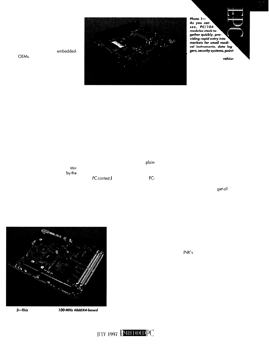
product development time and cost con-
straints.
Most engineers know the ‘x86 family
because of using ‘x86 desktop machines.
This abundance of “humanware” added to
the most cost-effective hardware and soft-
ware available is the lure for
system
So
far, ‘x86 hardwareapplications have
been limited only by the imagination! They
appear in telecommunications equipment,
process control, portable instruments, data
logging, medical instruments, gaming ma-
chines, vending machines, and navigation
systems-l could go on and on.
The market’s rapid growth has increased
demands on the design team to create
state-of-the-art products, minimize costs,
minimize risk, and shorten time-to-market.
The typical
product using embedded PC
hardware and software does not rely solely
on off-the-shelf items. The greatest value
added should always come from the propri-
etary content developed by the OEM.
DESIGN CHOICES
Designing a leading-edge product of-
ten doesn’t begin with leading-edge tech-
nology. In fact, the embedded market
allyrelieson technologyabandoned
desktop market.
You need to consider a number of
design choices if you’re going to arrive at
the ideal solution to a given problem. Any
project can encompass one or all of the
options available, depending on market
pressures and total anticipated manufac-
turing volume over the life of a product.
Taking the time to make the right deci-
sions about software and hardware is
crucial. When you select off-the-shelf hard-
ware and software, you enter a partner-
ship. Your partner is the hardware or
software supplier whose products you’re
incorporating.
Go past the specs to ensure there’ll be
adequate support both at the front end and
long term.
SOFTWARE SELECTION
What do you want-real time, a DOS
tailored for the embedded market, or
vanilla MS-DOS? A GUI?
Given that you’re entering the Embed-
ded
assume your goal is a
compatible system. But, what’s that mean?
In an embedded application, you’re prob
ably not concerned with running desktop
word-processing or spreadsheet software.
Games are also likely out of the question.
Usually, you want to write the custom
embedded application on a desktop PC
and possibly interpret the
data collected by the prod-
uct on a similar system.
Marketing may have
also determined that it’s
important to have a famil-
iar look and feel so the
ultimate end user can use
the product as intuitively
as possible.
Photo
high-performance
SBC
incorporating all the functionality of a typical desktop system
targets applications like medical imaging and high-speed test
equipment.
Therefore, you may also
be considering a GUI that
exhibits desktop charac-
teristics. Pull-down menus
and task-execution and
-termination buttonsare the
most recognizable fea-
tures employed in interac-
tive interfaces between hu-
mans and machines.
of-sale terminals, communi-
cations devices, and
lar navigation systems.
After marketing communicates the
system’s human-interface requirements, you
have to select the right combination of OS
and application software that most closely
matches product specification.
You’ve already chosen the PC architec-
ture because it has so much going for it in
terms of user familiarity. The problem now:
choosing from its abundant riches.
There are many excellent alternatives.
Faced with the challenge of picking the
“right” solution, you’ll tend to opt for the
most familiar. After all, less learning curve
means shorter development time.
Although this possibility is very tempt-
ing, I’d like to suggest that you ask the
providers of the various options out there.
Although none of us like to be sold on
something we’re unfamiliarwith,
the
facts before making a decision. A few
phone calls or E-mail messages will give
you a feel for the kind of support and
responsiveness you can expect. Remem-
ber, a quick response from a helping hand
can save the day when an important cus-
tomer demo is just hours away.
Whether you need a real-time OS, an
embedded DOS, flash file-management
software, windowing software, debugging
tools, or embedded kernels, the software
sponsors of
Embedded
PC
Design
Contest offer a wide range of products and
the support necessary to get products to
market quickly. Taking advantage of their
assistance is simply common sense.
So, you’ve compared the options and
selected the right software for the project.
Now comes the hardware.
HARDWARE CHOICES
Hardwaredesign methodologyfallsinto
four principal categories depending on the
size of
the
marketand stage in the product’s
life cycle.
49
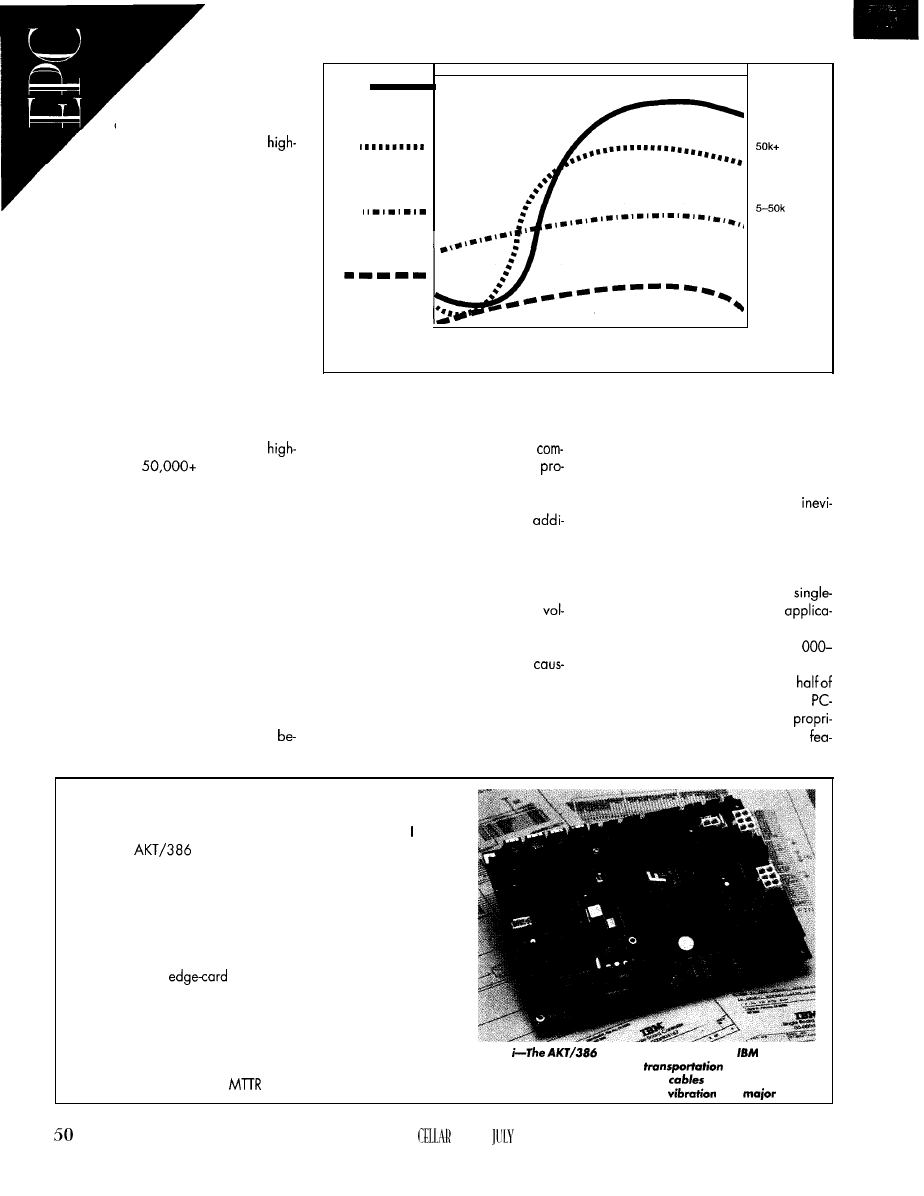
Figure 1 illustrates
typical product life cycles
when the four most common
design methodologies are used.
A product intended for very
volume production may actually
progress through all of the architectures
on its way to mass production.
However, time-to-market pressures of-
ten shorten total product market life to the
point where it no longer makes sense to
undertake wholly proprietary designs.
Therefore, more in-house designs are only
partially based on discrete components
that reflect the unique value-added pro-
vided by the OEM.
Selecting the appropriate architecture
depends in great measure on the ultimate
market for which the product is intended.
I N - H O U S E / D I S C R E T E C O M P O N E N T S
This choice is usually best for very
volume where
systems per year
will be produced. Here, the cost of goods
is likely to be the greatest concern.
However, this approach often requires
the highest front-end costs. The architecture
must be determined, components selected,
and prototypes built-all before the hard-
ware and software can be integrated, a
BIOS licensed and adapted, and an oper-
ating system ported.
Elan 300 series from AMD). These devices
get to market quickly to prove market
must then be integrated with the other
viability and gain a foothold ahead of
ponents to complete the design and
competitors. If the design achieves the
vide the system’s I/O and other functions.
desired results and production volumes
A design based on one of these devices
grow rapidly, a redesign is almost
often includes as many as 50-l 00
table in order to reduce product costs and
tional components. Obviously, the effort to
maintain or increase market share.
qualify, order, track, and inventory this
many components can only be justified by
S I N G L E - B O A R D C O M P U T E R S
extremely high-volume production.
The extremely wide selection of
Also, only these high-production
board computers for embedded
umes afford some measure of insurance
tions makes them ideal for products whose
against the risk of any single component in
volumes are not expected to exceed 1
a design reaching its end of life and
2000 units per year.
ing a complete system redesign.
Typically, these boards represent
the solution, as they only provide a
The extremely short product life cycles
inherent in the desktop mean that before
selecting your ‘x86-compatible compo-
nents, ensure that those components will
still be available when production begins.
A discrete component design often
gins with a PC-on-a-chip device (e.g., the
modules shown in Photo 1) help designs
tures of the product.
BACKPLANE-BASED AND STACKING
compatible “engine.” A second
Stackablecomponents (e.g., the PC/l 04
etary design incorporates the unique
In-House
Proprietary
Design
Single-Device
PC
Single-Board
Computer
Backplane-Based
or Stacking
Architectures
Proof of
Product
Market
cost
Product
Concept
Introduction Acceptance Reduction
Phase Out
Very High
Medium High
Medium
250-l 000
Low/ Proof
of Concept
l-500
Figure l-Selection of one of the four most common design methodologies depends largely on
the product’s expected production volume and life cycle.
From Backplane to SDPC-Based Design
A unique single-board embedded computer is the culmination of
a progression through several of the design methodologies
discuss. The
single-board transportation system controller
shown in Photo i is part of a fare-box controller design developed
by IBM Argentina’s Systems and Solutions Group for use on public
transportation systems.
The project began as an eight-board backplane-based design
used to prove the concept and enter the market. The next iteration,
a three-board PC/l 04 solution, reduced costs and increased
reliability from the
backplane design.
The decision to proceed with the final design was reached as
prospects for higher volume developed. As well, field experience
made it clear that even a ruggedized PC/l 04-based solution
wasn’t as reliable as a single-board design would be. Eliminating
board interconnects and interboard cabling increased reliability
while substantially reducing
in the field.
photo
CPU board developed by
Argentina
and ZF
Microsystems targets
applications. A
single-device PC eliminates many
and board intercon-
nects-a plus in an environment where
is a
issue.
CIRCUIT
INK
1997
Generally, these boards are best suited
to applications where cost is less of an issue
than performance. As a result, most of the
introduced currently tend to be pre-
mium priced, very high-performance
Pentium- or
designs like the
in Photo 2.
S I N G L E - D E V I C E P C S
These component-h ke devices from
S-MOS, or
Microsystems (e.g., the
386 module shown in the
and
described in
let
you include PC/AT
motherboard functions in proprietary de-
signs with minimal effort. They are usually
best-suited to higher volume applications
(e.g.,
systems per year).
Here, the development cost amortiza-
tion is less significant, and the purchasing
power is reasonably high. Therefore, these
solutions must be highly cost competitive
with in-house designs.
Single-device PCs have the advantage
that project development can be done
directly on the target processor that will be
used in the final product. This feature en-
ables shorter development cycles and faster
product introductions with almost no rede-
sign for high-volume production (seesidebar
“From Backplane to SDPC-Based Design”).
Single-board computersand backplane
or stacking architectures (e.g., PC/l 04)
lets
lower volume products go from concept
to product introduction without redesign.
These architectures are most appropriate
for production volumes of 250-l 000 units
per year and for proof of concept.
Their primary disadvantages appear
when market acceptance drives volume up
and the added cost of interconnects be-
tween the SBC or stacking module and the
proprietary technology makes cost reduc-
tion difficult without a system redesign.
Stacking modules can, ho&ever, be
ideal peripherals for adding plug-in op-
tions to any of the architectures.
G O O D L U C K !
Successful companies lead their mar-
kets by getting products out before their
competitors. They focus on their core com-
petency and manage their resources effec-
tively, thereby controlling their costs.
The brightest ideas are useless unless
they get to market first. Few remember the
second person to fly solo across the Atlantic.
Good luck with your entry in the Embed-
ded PC Design Contest!
David 1. Feldman is president and CEO of
in Pa/o Alto, California.
The founder and former chief executive of
Computers and the creator of the
PC/
concept, David has more than 25
in business management
and the embedded systems market. You
him
corn.
S O U R C E S
LCD controller
Apollo Display Technologies
M o r r i s A v e .
N Y 1 1 7 4 2
( 5 1 6 ) 6 5 4 - l 1 4 3
F a x : ( 5 1 6 ) 6 5 4 - l 4 9 6
Embedded PC Design Contest
4 Park St.
V e r n o n , C T 0 6 0 6 6
8 7 5 - 2 1 9 9
87 l-04 1 1
CPU, 1
M i c r o s y s t e m s
1 0 5 2
C t .
P a l o A l t o , C A 9 4 3 0 3
I R S
4 13 Very
Useful
( 4 1 5 )
F a x : ( 4 1 5 ) 9 6 5 4 0 5 0
414
Useful
4
15
Not Useful
If you feel you’ve paid enough, check out our
development tools for x86 embedded systems!
Cross develo
for 32-bit em
system
edded systems.
Boot code, locator, cross debugger.
Intel 386 and
P&l/ROM.
For Borland C/C++, Microsoft
C/C++, and Delphi.
Libraries:
700 Source Code: add
2
Professional.
real-time
kernel
for
Intel
higher.
for Borland C/C++,
C/C++, and
C/C++.
Libraries: 950 Source Code: add $1650
Professional, high-performance real-
time multitasking kernel for DOS
and
embedded systems.
For
Borland C/C+
C/C++, and Borland Pascal.
Libraries: $550 Source Code: add $500
Coming soon:
stack and FAT file system!
North America:
International:
On
On Time
88
Avenue
R E A L - T I M E A N D S Y S T E M S O F T W A R E
JULY 1997
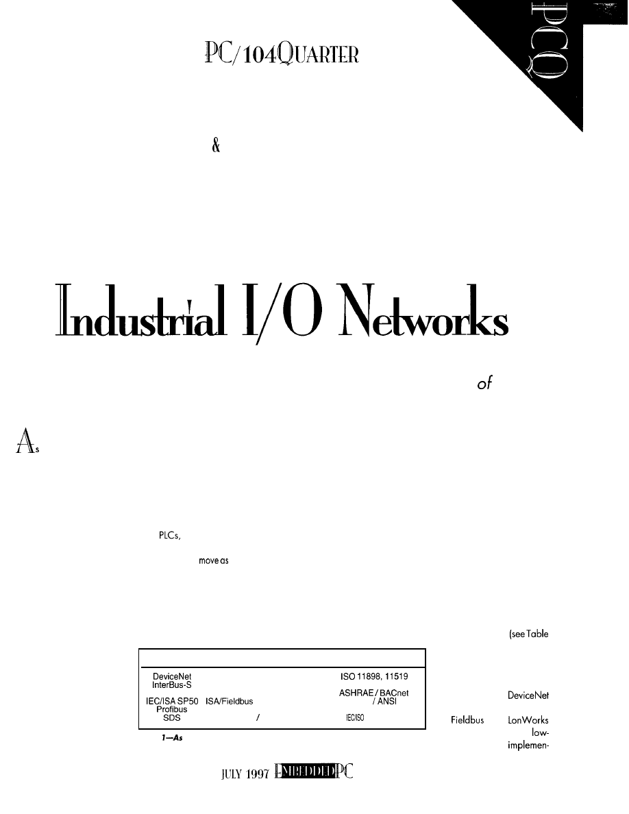
Mike
Justice
Phil Marshall
Although the desktop world essentially adheres to one network standard, the
variation in industrial applications has led to the development several
networks. Mike and Phil suggest how to determine which standard you need.
with any network, an industrial net-
work is a common communications link
between two or more devices. But, due to
the unique requirements of manufacturing,
separate networking technologies have
developed.
coax or fiber cable media) since they must
provide noise immunity and dependability
in harsh electrical environments. As well,
the media used in the factory has different
packaging and support hardware (e.g.,
hubs and connectors).
1000 I/O points can be transferred in a
single message, usually only a few bytes of
data are required per transaction.
These industrial networks-generally
called “fieldbuses’‘-connect PCs,
industrial I/O, operator interfaces, drives,
or any device needing to communicate
with other pieces of a control system.
OFFICE VS. FACTORY
In
office
automation,
the goal usually is to
much data as possible between two
points on an occasional basis. The transac-
tions are often much larger than what’s
commonly found on an industrial network.
In industrial applications, you control
I/O and continuously require the status of
the I/O connected to, say, a PLC. While
As well, you need the data continuously
and in a predictable time frame. A con-
veyor application, for example, might be
on every token rotation of the network to
maintain synchronization, drive speed, and
torque.
The cost per node differs significantly as
well.
Industrial fieldbuses share several char-
acteristics that distinguish them from their
office relatives (e.g., Ethernet). For one,
they are deterministic in nature, thus pro-
viding predictable performance.
And, while fieldbuses
aren’t as fast as office net-
works, data rate is probably
an overused criteria for net-
working. After all, the mes-
sage profile is different in the
two applications.
WHY SO MANY?
Given the myriad needs in manufactur-
ing environments, there’s a proliferation of
industrial networkson themarket
1). tow cost and high speed
with a deterministic architec-
ture are only two require-
ments of networks for local
I/O devices (e.g.,
and SDS).
Network
Technology Developer
Year Standard Organization
Allen Bradley
1994
Phoenix Contact
1984
DIN 19258
LonWorks
Echolon
1991
Foundation
1992
IEC 1158
850
Siemens PTO
Honeywell
1994 1994
DIN 19245 11989
Industrial networks also
tend to be more robust (e.g.,
Table
you see, most network schemes were developed by different
corporations and are maintained by different standard organizations.
and
are also designed for
cost device-level
53
Application
LonWorks
Profibus
SDS
Packaging
Conveyor
Building Control
Process Control
X
each network type meets the particular needs of a niche.
tafions.
were originally designed for, greater dis-
tances are required, so
t h e y
sacrifice speed.
Profibus and
are for a higher
level of communications (e.g.,
controller communications). They let the
of m a n u f a c t u r i n g p r o c e s s , p r o d -
uct quality, and plant productivity.
For long-term flexibility, use an open
network. Thisstandard providescompatibility
so that you can select vendors based on
cost, availability, and functionality
Some network protocols meet the spe-
cific
particular
application (e.g.,
for drive applications). Others are
designed for use in single point I/O (e.g.,
and SDS).
Obviously, the best
for one ap-
plication is not best for another. In applica-
tions like packaging machinery, performance
is key. Process control, on the other hand,
cares about distance and cable length.
C H A R A C T E R I S T I C S
Someofthe most importantdetailsabout
an industrial network are its physical char-
acteristics, speed, distance, cabling, and
communication methods (see Table 3).
Frequently, the need for speed is bal-
anced by distance issues. Maximum dis-
tance usually causes minimum speed.
Twisted pair is the lowest-cost network
solution as well as the easiest to install and
Network
Speed (bps) Distance (m)
Cabling
Comm. Type Max. Devices
500
TP, signal power
64 nodes
TP, fiber
256 nodes
LonWorks
up to
TP, fiber, powerline
1900
TP, fiber, radio
128 nodes
24k
TP, fiber
500
power
127 nodes
64 nodes
Table 3-Sometimes, you can determine which network is best for your application
by looking at the specs.
stands for twisted
pair, while MM and M/S refer ta multimaster
and master/slave, respectively.)
maintain. Its disadvantage is its lack of
electrical noise immunity.
Fiber-optic cable is good for distance,
conductivity, and electrical noise immunity.
But, it must be cut to fixed lengths and uses
specialconnectors, complicating installation.
Radio is used for remote areas, where
wiring and distance is a
problem.
installing radiocommunications is
cult, but cost, speed, two-way communica-
tions, and radio interference complicate
the process.
The two communication methods are
multimaster and master/slave. In a multi-
master network, you need to know how
arbitration specifies
priority
and
performance.
The number of online intelligent devices
(e.g., PCs) can also be a factor. A multi-
master network lets each master communi-
cate with other masters and slave devices
without working through a single device.
Although most networks are still mostly
single master and multiple slaves, the soft-
ware enabling multimaster capabilities is
evolving to truly distributed systems.
A P P L I C A T I O N N E E D S
Network design balances several fun-
damentally opposing issues-speed, dis-
tance, and cost. As speed and distance
increase, so does design sophistication,
resulting in higher cost. low cost is the
goal, in restricting
distance
and
speed, you
restrict the applications it works for.
In a typical packaging application,
where a local machine puts a product into
a box or package, the machine is in a small
geographic area and has a large number
of DIO points. While distance is not an
issue, performance and cost of the many
I/O points are important.
JULY 1997
Table
can
have
cake
and
it,
Each gain comes with a
specific tradeoff.
InterBus-S, Profibus, and SDS qualify as
In building automation, dataaboutdoors,
good choices since they provide I/O with
windows, heating, and air conditioning
good performance.
ates a profile for energy and security
In a conveyor application, many DIO
trol. The I/O requirements are digital and
points are spread over a large area.
analog with single pointsover a widearea.
ability of data packets, networking
Performance isn’t usually an issue with
and speed are most critical. Again,
building-automation systems. A or 1 O-s
InterBus-S, Profibus, and SDS
scan time is considered fast.
are good choices.
and
are well-suited for
S
tart programming devices today with the lowest cost and highest per-
formance CERTIFIED programmers. Enjoy a no hassle user interface for
ALL versions of Windows and DOS. Works with any PC of any speed
without a hitch. Device libraries added in less 2 hours to our Web cus-
tomer support section. Unique programming head options for gang pro-
gramming most microcontrollers and memory devices. Direct Docking
PLCC, DIP... programming heads. Evaluate a unit today
with
satisfaction guaranteed
or
YOUR
MONEY BACK!
(no penalties or restocking fees if unit is returned).
Call Today in USA
Fax: 303-733-6868 or Visit our Home Page:
www.logicaldevices.com
motion networks, since theysupporta huge
number of I/O over very large distances.
Process-control applications vary
widely-from large oil refineries to small
chemical processes. In general, they use a
lot of analog inputs and outputs and only a
few digital I/O. Because it’s mostly ana-
log, the price is high. Data and network
reliability is extremely important.
Performance of the scanning of I/O can
be an issue, but most systems have only a
few points requiring fast scans.
and Profibus PA are preferred be-
cause they can handle a lot of analog I/O
spread over large areas.
While it would be great to quantify the
selection of a fieldbus, the process is closely
related to the type of application. One
application’s need often has an opposing
tradeoff (see Table 4).
For example, if you need high speed
and high I/O density, your system is prob-
ably confined to a small area. If you have
a large number of nodes, then system
density is probably low and spread out
over a large area.
MACHINE-CONTROL EXAMPLE
The real-time control-systems division at
Advanced Technology and Research (ATR)
was contracted by General Motors to pro-
vide an open-architecture controller to sup-
port work with NCMS on the Next Genera-
tion Inspection System Project (NGIS II).
This controller serves a test bed for
developing machine monitoring and
machine measurement techniques to im-
prove the accuracy of milling operations.
ATR was to retrofita K&T 800
axis milling machine in the GM Powertrain
engine-prototype lab with an RCS2000
open-architecture CNC controller. Probes,
machine monitors, and sensors interface to
the controller through open
Profibus was chosen for several reasons.
In addition to gaining international support,
the speed and determinism of Profibus DP
(12 Mb) was well within GM’s require-
ments. A milling machine must scan many
digital and analog I/O points quickly.
The bus needed to
be
fast, deterministic,
and either open or a standard. The scan
time for reading and writing data had to be
in the millisecond range and be predict-
able. Profibus DP proved to be the best fit.
So far,
II has been a success. ATR
is presently testing the machine with
drives and an RCS2000 controller.
C O M M O N I N T E R F A C E S
Standardizing the interface to the soft-
ware and hardware enables users to select
the industrial network that best fits the
application, preserving the investment in
software and core hardware.
Using the PC/ISA or PC/ 104 computer
bus as an example, we developed a set of
PC/ISA and PC/ 104 boards that share the
same hardware and software interface
with the user. Each industrial network is
implemented on the coprocessor board
with the network connection and all the
network-specific software and firmware
running on the adapter board.
The interface to the user is via dual-port
memory and a selectable interrupt. The
memory structure is the same for each
adapter.
For example, the first 1 KB is used for an
image of the inputs and outputs. The sec-
ond 1 KB handlescommunication messages
to and from the board. The third area holds
a set of simple command and status bytes
that provide commands and information
about the adapter.
providing the same interface to each
industrial network and a set of standard
drivers for DOS, QNX, and Windows
3.1
and NT, the user can easily write
one application and use it with different
networks. The industrial network then be-
comes just another simple component of
the application-not a
problem.
Manufacturers are faced with the chal-
lenge of supporting various networks while
minimizing costs. The PC/l 04 architec-
ture solves this problem by providing a
mechanicallyrobustand stabledesign plat-
form while leveraging a large existing
design base of products.
Since the
and ISA bus are
fundamentally electrically identical, we
could port all our ISA-based products to the
PC/l
while maintaining compat-
ibility with the existing base of developed
drivers.
N O T “ O N E F O R A L L ”
Frequently, we’re asked which network
is best or which network is going to win the
war.
Our answer: many different networks
will survive, given the sheer number of
applications. No single network can ad-
dress all the needs of all applications.
So,
use the information you can glean
and select an open-architecture network
that enables your application to use the
best attributes of that network.
is
Systems, a company specializing in provid-
ing industrial
adapters for PC,
PC/
and custom OEM products. He is
the executive director of the
Club
and has been involved with industrial com-
munications for 18 years. You may reach
Mike at
Phil Marshall is sales manager at SMSI.
He has marketed and sold industrial
products for the last IO years.
REFERENCE
General Motors, Ford, and
Chrysler, OMAC Paper,
S O U R C E
Network
products
Synergetic Micro Systems, Inc.
2506 Wisconsin Ave.
Downers Grove, 605 15
(630) 434-l 770
Fax: (630) 434-l 987
4
16
Very Useful
417 Moderately Useful
418 Not Useful
IF YOU’RE EMBEDDING A PC,
TAKE A LOOK AT THESE
No, it’s not a very large chip, it’s a very
small computer. A complete,
386SX computer in a 240-pin
mount package just
that mounts on your board like a chip.
Harsh Environment?
Forget unreliable cables and vibration
problems. Everything you need is built
into the
It boots from its
internal Flash disk and even has 256K of
user available program space. There are
two COM ports, a parallel port,
core
logic, keyboard speaker ports, IDE
and floppy disk support, and 2Mb of
internal DRAM with support for up to
64Mb externally. Only 5V at 2W (power
management sleep modes available).
Mounted directly on your proprietary
board, connections are rock-solid even in
harsh conditions.
A familiar platform.
The
is PC/AT compatible, so
all your standard development tools will
work perfectly.
BIOS DOS license included.
No licenses to negotiate. Power on the
and you have a DOS prompt.
1997
The creator of the
concept brings
you more features per dollar than any
CPU on the market.
up to
DRAM
Flash, floppy, IDE,
4 serial, 2 parallel ports!
The
development kit comes
with everything you need to put your
project on the fast track to market:
hardware, software, schematic and
component libraries. It includes both AT
and
expansion busses.
Jointly developed by IBM @and and ZF
for the transportation industry. Only 5.75”
x
8 serial ports,
ports,
interface, slave processor
controls RS485 multidrop network, and a
resident interface for GPS.
Inc.
1052
Court
Palo Alto, CA 94303
Tel: l-800-683-5943
Fax:
57
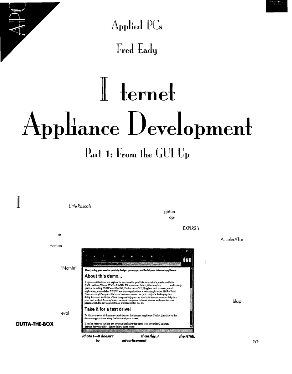
n
And you
thought
you
were unique? Nah! Even the embedded world wants to
get on the Internet. Fred shows us some new tools that make it easier for
companies to upgrade their clients’ products remotely via the Internet.
feel like Buckwheat in the
in quickly getting an Internet Appliance to
Rascals’ single-word-speaking secretary
movie when he chased down the duck and
market. It has everything you need to
would say, “Uh-huh.”
got a dollar bill tied to its leg. He was singing
Internet Appliance development system
Just 10 minutes. Everything needed to
and dancing, “I’ve got a dollar, hey, hey,
erational in minutes.
run the initial demo is preloaded in the
hey. Got a dollar today, hey, hey, hey.”
After reading the 0.634” of start-up
flash.
Getting further into
duck
story, Butch
documentation, I was up with a working
You get a couple QNX Ethernet cards
(the
bully
of the Rascals) had a problem. He
demo in about 10 minutes. As Uh-Huh, the
and a Rockwell 33.6
Modem
wanted to steal the
Womun
Hater’s Club car for the big race,
but Porky and Buckwheat were
guarding it.
Butch’s motto was,
beats a duck and a buck.” He tied
a dollar to a duck’s leg and got
Porky and Buckwheat to chase the
dollar-bill-totin’ duck. Butch and
his sidekick, Worm, got away with
the car.
At first glance,
I'd
probably
chase a duck tied to this
kit.
INTERNET
The EXPLR2 Internet Appliance
Developer’s Toolkit is designed to
aid theembedded design engineer
58
get any easier
“modified”
source add an INK
to the top of the
window.
CIRCUIT CELLAR INK JULY 1997
kit with the EXPLR2 kit, too. And,
all thecablesand what-nots are in
the box.
followed the instructions for
setting the Ethernet card and
modem jumpers and plugged the
two cards into the open ISA slots
on the EXPLR2 board. I added a
keyboard, mouse, display, and
standard PC power supply.
I fire it up, and
I’m look-
ing at Photo 1. A phone line and
some ISP (Internet Service Pro-
vider) info later, I was on the ‘Net.
I’m jumping around in the
kitchen, singing like Buckwheat,
and you’re shaking your head,
“Fred got this neat embedded
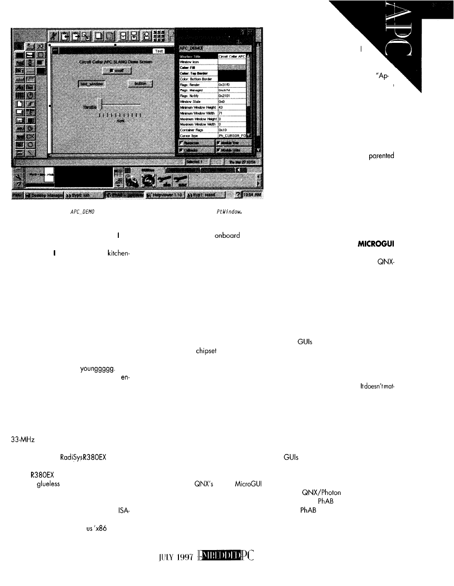
Photo 2-Who cares about making a real application. I could spend days here turning all those
knobs1 Notice that the
I
created is an instance of the Photon class
tern in the mail, and now he thinks he can
get on the Internet with a toaster oven. bet
he braided his hair like Buckwheat, too.”
Otay. Otay. may be a singing,
dancing, mad-duck-chaser with braids, but
I know what an “Internet Appliance” is.
Do you? Well, you know what the Inter-
net is, and you know what an appliance is.
That’s an Internet Appliance. It’s your ver-
sion of a toaster or dishwasher for the
Internet-a specialized piece of embed-
ded hardware and firmware you design to
perform some particulartaskvia the Internet.
A 455 ROCKET
If you don’t remember the Oldsmobile
455 Rocket V-8, you’re
In its
time, it was the biggest displacement
gine
you
could buy off the showroom floor.
It was built for speed.
Just like the 455 Rocket was built to go
real fast, the EXPLR2 Internet Appliance
system board was designed to be both
flexible and functional. It’s based on the
C-Step Intel ‘386EX processor
and surrounded by a full set of peripherals,
compliments of a
embed-
ded system controller.
The
is specifically designed to
provide
support for the ‘386EX.
It’s got most everything-a DRAM control-
ler, keyboard/mouse controller, real-time
clock, enhanced IDE interface, and an
bus controller. Of course, all the goodies
are PC compatible to keep
embed-
ded bit shifters happy.
To jazz things up, the Intel and RadiSys
folks threw in functional
Port 80
POST LED circuitry
and
a PCMCIA interface.
When all is said and done, the hard-
ware consists of:
l
an EXPLR2 system board with mouse,
keyboard, standard PC power supply,
and monitor
l
a host PC (‘486 or higher) loaded with
QNX and the normal complement of
peripherals
l
a QNX-based Ethernet link between the
host and EXPLR2
l
a 33.6 Rockwell
modem on the
EXPLR2 for Internet access
BODY BY FISCHER
All the power that 455 Rocket could
muster wouldn’t push it along the highway
withoutsomesupportingcomponents (e.g.,
tires, a crankshaft, a frame, and a sturdy
body). Remember, Butch stole the whole car,
not just the engine.
I could power up the toolkit system board,
drop it onto some hot embedded asphalt,
and obtain minimal computational results.
There’s nothing special about the hardware
functionality.
Or, I could add
Photon
and a “just-in-time-compiled-programon-the
fly” programming language from Cogent
Real-Time Systems.
In
case
you’re not mechanically inclined,
let me put this Photon/SLANG thing in
perspective. You just designed and mar-
keted a unique Internet
Appliance. Some fancy
marketing engineer named all
the buttons.
Way down in the menu structure, a
selection-button label is misspelled.
propo” is something you thought you ate
with cornbread. Well, it should spell “Apro-
pos,” and you can’t order it at the diner.
You have more of these devices with the
misspelled label out there than you want to
think about. And, you can’t tell your clients
to stop using their products for a couple
hours while you download the fixes. Most
of them rely on the appliance you
to keep their businesses profitable.
And, by the way, your little invention
was sold all over the world. That means
different time zones. Someone somewhere
is using it all the time! You’re hosed!
(Where did you put that resume?)
But, you created your GUI sibling with
Photon and SLANG.
PHABULOUS PHOTON
Photon is a graphical user interface
environment for the QNX RTOS and
based applications. It’s similar to any other
GUI you may have encountered in your
development travels.
Just like Bill’s Visual stuff in the DOS
world, Photon is an event-driven environ-
ment. User input via mouse or keyboard is
processed as an event, and a correspond-
ing output is produced.
Bill’s
tend to be largish because
they’re not intended for a classical embed-
ded environment. Photon is inherently tiny
but can be scaled to any proportion.
Thus, it can be used in embedded and
not-so-embedded applications.
ter if you’re running Photon on a stingy
embedded design or a full-blown PC-the
look, feel, and results remain the same.
Photon has the added advantage of
being microkernel based, enabling it to
work easily in network-intensive applica-
tions. Right there beside QNX.
aren’t grown on trees and don’t
come preapproved in the mail. Somebody
and something must be employed to make
a pleasurable interface.
In the
world, that devel-
opment tool is
(Photon Application
Builder).
assembles and generates
the GUI objects the user manipulates as
well as the application interface C code that
makes the interface come alive.
59
80251 Embedded
Midwest Micro-Tek is proud to offer
its newest line of controllers based
on the
architecture.
The 8031 comes in at a surprisingly
Cost of $89.00
(100 quantity).
80386
protected mode
family
real mode
family
R3000,
l
Compact,
fast interrupt response
l
Preemptive,
based task scheduler
l
Mailbox, semaphore, resource, event, list,
buffer and memory managers
l
Builder
l
documentation
l
No
source code included
For a
AMX,
Phone: (604) 734-2796
F a x :
E-mail:
W e b :
KADAK Products Ltd.
206 1847
West Broadwa
Vancouver, BC, Canada V J
If you’re interested in getting the
most out of your project, put the
most into it. Call or Fax us for
plete data sheets and CPU options.
MIDWEST MICRO-TEK
I’
2308 East Sixth Street
Photo
I didn’t have to write any complicated code to make any of this happen.
consist of windows, menus, dia-
logs, icons, buttons, labels, and supporting
user-written or machine-generated code.
handles the design and creation of
all these ingredients.
Its strength lies in the fact that you the
developer can focus on the problem at hand,
not the code. Buttons and labels are encap-
sulated into what Photon calls “widgets.”
Using
widgets are created,
moved, and processed by a simple mouse
click. Each widget has a set of parameters
or resources controlled within the
framework atcreation. These resources can
be varied on-the-fly in run
SLANG.
In addition to the physical control of a
widget,
permits working code to be
attached to a widget’s event-generation
properties. In other words, when a button
within the GUI is selected, an event is
triggered that invokes an application-spe-
cific call-back algorithm.
This callback is usually connected to a
window, dialog, or menu. Most of the time,
the callback is laced with user-written C
code to perform a predetermined function.
The raw interface code is generated by
not the programmer. So, the inter-
face can come alive without you writing
any code. Think about it. You can test the
GUI interface for look and feel before
committing to any application code.
Let’s face it. Most of the problems with
creating GUI interfaces are called “end
users.” I don’t care how pretty or functional
the programmer thinks the GUI is, end users
always have the final say. With
you
can create a GUI for them while
they
watch!
Once you nail down the interface, you
can fine-tune the GUI with your own C
verses. While Photon (and
every
other
GUI,
for that matter) was designed to work this
way,
has a secretweapon-SLANG.
SLANG takes the place of C in the
environment. Normally, you design your
GUI interface and use
to generate the
C back-bone code that makes the widgets
work at their minimal level.
With SLANG, you design the interface
without generating the basic
C code.
You then load the codeless
widget image into the SLANG environment.
Using SLANG syntax that’s structured to
closely resemble native
command
syntax, you logically implement the call-
back structures just like you would with C.
The developers at Cogent tell me they only
use C for the down-and-dirty driver stuff.
If you’re not intimately familiar with LISP
and C, SLANG
to be a littledifficult
to understand at first. Once you’re high on
the learning curve, here’s what SLANG buys
you. For every 1 O-l 5
write
in C call-back code, you write on average
l-2 lines of SLANG code.
Also by using SLANG, you can modify
appearanceand
out (yes, without) stopping or interrupting
the running application. So, you can change
the GUI’s look and feel in real time.

your local
Thus, those
your nifty Internet
With SLANG, you
can debug the
tion-GUI and all-in real
time. Since QNX is network
natured, you can even debug and
modify SLANG applications remote to
Appliance can be squashed without inter-
rupting the user or the program. Program
updates can be applied on-the-fly, totally
transparent to the user.
The bestwaytofullydescribethismiracle
is to show
you
how it’s done.
CODE
Rememberthosecoupleof Ethernetcards?
Well, the other network card goes into a
host PC running the QNX demo system that
comes with the toolkit.
The idea is to link the host PC with the
EXPLR2 board via Ethernet and use the
power of QNX IPC (Interprocess Communi-
cation) and SLANG to rapidly debug and
deployyourapplication.
IPC link,
you can control the application running on
the EXPLR2 from the host PC and vice versa,
The EXPLR2 QNX software suite consists
of a 30-day license for full-blown QNX
4.23,
C 10.6, Photon, and QNX
on CD. A
full-function ver-
sion of SLANG comes on another diskette.
The set includes an abundance of work-
ing Photon and SLANG programming ex-
amples bundled with their complete (and
commented, I might add) source code.
For guys like me that need to show this
stuff via the printed
scatter it about
the Internet, there’s a snap-shot program for
screen captures as well as a graphic viewer
among the many utilities on the CD.
One handy utility,
J
ump Gate,
enables
me to transfer programs between
host
and EXPLR2 for execution. I can also import
a screen from the EXPLR2 and manipulate
the application on the host PC as if it were
physically on the EXPLR2.
Photo 1 was generated by sending the
host-based
utility to the EXPLR2
and executing it there against the Web
screen. I sent the resulting screen capture
back to the host PC via the Ethernet link and
QNX IPC.
The QNX Ethernet connection along
with IPC features within the QNX OS lets
the EXPLR2 be loaded directly from a spe-
cific directory on the host
PC (/home/
The EXPLR2 board
listing
at that Load statement. might be a
by trade, but I know how to
widget around in QNX.
Initiate
session with Photon window manager
Declare a global name
Load Photon Widget convenience functions
Load support for loading windows created in
and convert window created in
using wload function.
Set first item returned
definition to be variable
named win.
win =
Normally, user-written call-back functions reside here
Start an infinite event loop to handle Photon events. I can also
use a call to
here, but then I can't intervene
after each event.
while
sees the host PC’s EXPLR2 directory as if it
were its own. Conversely, the host PC sees
into the flash file system on the EXPLR2
board!
The EXPLR2 can be made to boot over
the network or from its
flash.
Booting from the network lets the developer
quickly assemble an application and test it
by putting the required code modules in the
PC EXPLR2 directory and starting the appli-
cation on the EXPLR2 to bring them online.
Changes are implemented by modifying the
required module on the host PC and restart-
ing the application.
When debugging is done, bring your
application to life from flash by loading the
appropriate
C, and SLANG modules
into the EXPLR2 host directory and down-
loading the resultant
file
image to the EXPLR2
board’s
flash.
All the utilities to perform these
tasks are included with the EXPLR2 toolkit.
instantlyseethechanges
you make. Imagine skipping the compila-
tion and reboot steps and updating your
application in real time.
Yep, you can enter a line of code and
see the result while your application is
running! At that point, you can either incor-
porate it or trash it. That’s the power of
SLANG.
L E F T W I D G E T S
I’ll show you how it works by creating
and manipulating some widgets in a win-
dow with
Photo 2 looks into the
application I call
apcdemo.
Before I can manipulate the widgets, I
tions are established in the initial
session. For clarity, each widget’s name is
displayed as its initial text attribute.
After placing all the widgets in the
window, I generate the application using
Generate function. Generate
builds some backbone C code and a file
called
load into SLANG for manipulation.
Normally, using
only, I would
Ma ke the application that generates all the
code necessary to run the application.
Listing 1 is the SLANG load procedure
saved on the host PC as
sl angcode.
APC
window starts SLANG and sets
the
ronmentforloadinganapplicationwindow.
The Photon environment allows up to
nine
windows. To do on-the-fly
changestothe
APC
applica-
tion, I open
and issue ssend
slangcode.
The program ssend
to
a run-
ning SLANG program (e.g., slangcode)
and enables the user to send commands
without exiting the event loop of the at-
tached process. When sl angcode>
app and ready to issue change orders.
INK
1 9 9 7
RIGHT WIDGETS
The application con-
sists of a base window and
fivewidgets. Ci rcui Cel 1 ar
APC SLANG Demo Screen is a
label widget. The
f widget is an
on/off push button.
Let’s assume we need a landing-gear
push button in an aircraft application. To
= “GEAR”: in
What happens? Yep, it says GEAR.
Thisbutton
indicatorthatchanges
color when the button is pushed. This op-
eration is inherent to the widget, but I can
use SLANG to pick the color if wish.
Follow the commands through in Photo
3, and note the results in the application
window. That’s how SLANG works.
I can do all sorts of things to the widgets
from t
t y
p In fact, any widget resource
that can be program controlled can be
changed with this method. All that’s left is
to write and insert SLANG call-back code.
STILL RACING ON
While the software is solid and the
development hardware well thought out, it
takes time to navigate through the kit’s sea
of documentation. An inexperienced QNX
user will undoubtedly need to call for help.
I managed to hose my server’s Internet
mailbox because the Web demo didn’t log
off cleanly. One thing led to another, and
I found I’d also corrupted the SLANG demo
and snap-shot application while trying to
fix the mailbox problem. It wasn’t a pretty
sight, and I ended up reloading the entire
development package-more than once!
suggest you read all the supporting
documentation before diving into this kit.
And, if you’re not familiar with QNX, learn
some QNX basics and talk to some expe-
rienced folks before you begin.
I found the technical support from all
parties involved to be very good. Use them
as resources. It will save you time and
frustration.
Next time,
mix SLANG and Photon
into some hardware and cook up a useful
application.
Fred Eady has over 20 years’ experience
as a systems engineer. He has worked with
computers and communication systems
large and small, simple and complex. H i s
forte is embedded-systems design
Fred may be reached at
SOURCES
SLANG
Cogent Real-Time Systems
168 Queen St. S, Ste. 205
Mississauga, ON
Canada
1 K8
(905) 8 12-9628
Fax: (5 10) 472-6958
Photon
QNX RTOS
QNX
175
Matthews Crescent
Kanata, ON
Canada
1
(613) 591.0931
Fax: (613) 591-3579
Internet Appliance Devel-
oper’s Toolkit
Corp.
15025 SW
Pkwy.
OR 97006.6056
(503) 646-l 800
Fax: (503) 646-l 850
BBS: (503) 646-8290
4
Very Useful
420 Moderately Useful
42 1 Not Useful
3 PAR (32 BITS MAX)
32K RAM, EXP
-STANDARD PC BUS
LCD, KBD PORT
BATT. BACK. RTC
IRQO-15 (8259 X2)
0237 DMA 0253 TMR
-BUILT-IN LED
-UP TO MEG ROM
-CMOS NVRAM
USE TURBO C,
BASIC, MASM
RUNS DOS AND
WINDOWS
EVAL KIT
UNIVERSAL
PROGRAMMER
-DOES
8 MEG EPROMS
-CMOS, EE. FLASH, NVRAM
EASIER TO USE THAN MOST
POWERFUL SCRIPT ABILITY
MICROCONT. ADAPTERS
PLCC, MINI-DIP ADAPTERS
-SUPER FAST ALGORITHMS
OTHER PRODUCTS:
8088 SINGLE BOARD COMPUTER . . . . . . . OEM
‘95
P C F L A S H / R O M DISKS
16 BIT 16 CHAN ADC-DA
. . . . . . . . . . . . . . . . . . 21 . . . . . 75
C CARD . . . . . . ..*............
WATCHDOG (REBOOTS PC ON HANGUP) . . . . . 27 . . . . . 95
l
EVAL KITS INCLUDE MANUAL
BRACKET AND SOFTWARE.
M V S B O X
8 5 0
5
YR LIMITED WARRANTY
FREE SHIPPING
HRS: MON-FRI
EST
a
M E R R I M A C K , N H
.
( 5 0 8 ) 7 9 2 9 5 0 7
6 4
Touch The Future
LCD Touch Monitors
L C D T o u c h S c r e e n s
V G A L C D D i s p l a y s
LCD Controllers
ISA,
Analog, Video
EARTH
lowest Prices on
Computer Technologies
27101
Aliso Creek Rd
154 Aliso
CA 92656
Ph: 714-448-9368 Fax: 714-448-9316
FREE CATALOG available at
INK JULY
1997
DEPARTMENTS
From the Bench
Silicon Update
Jan Axelson
Using Serial EEPROMs
Part 1: General
f your project
needs a modest
amount of nonvolatile.
read/write memory, serial
EEPROM may be the answer. These
tiny, inexpensive devices are especially
useful for minimizing the number of
I/O lines, cost, or physical size.
Serial EEPROMs most commonly
store user data-settings for
control devices, phone numbers, secu-
rity codes, or anything that once was
set with DIP switches. You can also
store error codes, diagnostic informa-
tion, usage records (e.g., times, dates,
counts), and instrument readings.
In some cases, serial EEPROMs can
even store program code. Parallax’s
BASIC Stamp and similar products use
them to store user programs in the
form of BASIC language tokens.
This series is a guide to choosing
and using serial EEPROMs. In Part
1,
I
compare the three major interface
types-Microwire, SPI, and
In Part
show you how to program and
read all three types from a PC standard
parallel port.
THE BASICS
Serial EEPROMs use a synchronous
interface. Both the EEPROM and the
chip controlling it use a common clock,
and clock transitions signal when to
send and read each bit.
66
Issue 84 July 1997
Circuit Cellar INK@
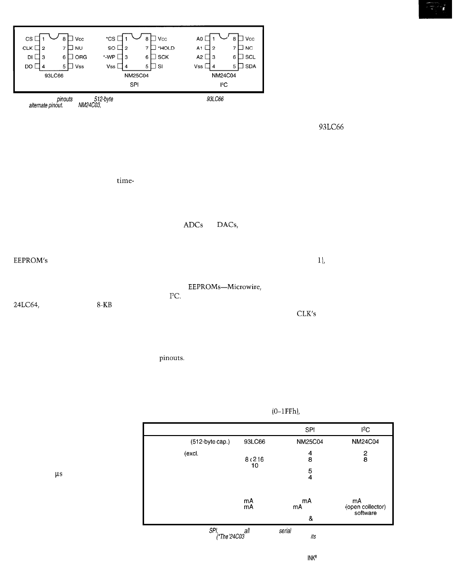
Microwire
Figure
l--Here are
for three
serial
EEPROMs. The SO/C version of the
is available in this
and an
On the
pin 7 is Write Protect.
Although synchronous serial chips
require minimum clock frequencies,
the clock for serial EEPROMs can be
as slow as needed, and the clock signal
doesn’t need to be symmetrical. The
controlling device can toggle the clock
at its convenience, up to the maximum
speed. There’s no need for a fixed
base.
Serial EEPROMs typically have just
eight pins-power and ground, one or
two data/address lines, and a clock
input, plus up to three other control
signals. Unlike parallel EEPROMs,
which add pins as the number of ad-
dress and data lines grows, a serial
physical size doesn’t have
to increase with capacity.
Capacities begin at 128 bytes. As
with other memory, maximum capacity
has increased over time. Microchip’s
for example, is an
chip.
The EEPROMs use CMOS technol-
ogy, so they consume very little power.
Currents are as low as a few microamps
in standby mode and a milliamp when
active.
The synchronous interfaces aren’t
intended for use over long distances.
For that, use RS-232 or RS-485. How-
ever, cables may be as long as 4 m in
some cases-longer if you add stronger
drivers and buffers.
Depending on the device, the maxi-
mum clock speed for accessing serial
EEPROMs can be over 2 MHz. But
because it takes eight clock cycles to
transfer a byte and the master also has
to send instructions and addresses, the
maximum data-transfer rate is no
more than -4 per byte.
Write operations take much longer
because the EEPROM needs several
milliseconds to program a byte into its
memory array. During this time, the
master can’t read or write to the chip,
but it can do other tasks not involving
the EEPROM.
With use, EEPROMs eventually lose
their ability to store data. So, they’re
not suited for applications where data
changes constantly.
National’s COP888 is an example
of a microcontroller with a Microwire
interface built in. Though it’s com-
monly called a three-wire interface, a
complete link actually needs four
signal lines plus a common ground.
These days, most are rated for a
minimum of 10 million erase/write
cycles. That’s fine for data that changes
occasionally or even every few minutes.
But, if you need unlimited read/write
cycles, use battery-backed RAM.
Microchip’s
is a 4-Kb serial
EEPROM with a Microwire interface.
It has two data pins, DI (data in) and
DO (data out), as well as a clock input
(CLK) and a chip select (CS).
Besides EEPROMs, other compo-
nents with synchronous serial inter-
faces include
and
I/O
expanders, clock/calendars, and display
interfaces. Multiple devices connect to
one set of lines, with each chip having
its own Chip-Select line or firmware
address.
Additional inputs are for memory
configuration (ORG), which determines
data format as 8 or 16 bits, and program
enable (PE), which must be high for
programming. Setting ORG high saves
time because you can program and
read two bytes with one instruction.
The EEPROM understands seven
instructions-Erase/Write Enable and
Disable, Write, Read, Erase, Erase All
(sets all bits to and Write All (writes
one byte to all locations).
There are three major types of inter-
Figure 2 shows the timing for byte
faces for serial
read and write operations. Each instruc-
SPI, and
The different types vary
tion must begin with a Start condition,
in speed, number of signal lines, and
which occurs when CS and DI are both
other details.
high on
rising edge.
To see how the different interfaces
compare, I describe a 4-Kb EEPROM of
each type. Table 1 summarizes the
major features, and Figure 1 shows
their
All EEPROMs with the same inter-
face behave in a similar way, though
they may vary in the number of address
bits and other details (e.g., whether
there’s a write-protect pin). Always read
the datasheet for the chip you’re using!
The master must bring CS low after
each instruction except sequential
reads. When CS is high, the EEPROM
is in standby mode, ignoring all com-
munications until it detects a new
Start condition.
To write to the EEPROM, the master
must first write an Erase/Write Enable
instruction to DI, followed by a Write
instruction, the address to write to
and the byte or word to write.
MICROWIRE
Microwire is the oldest of the three
interfaces. National Semiconductor
introduced it, and other manufacturers
now support it as well.
Interface
Microwire
Example device
Source
Min. interface
GND)
Data width (bits)
Max. clock speed (MHz)
Write (busy) time (ms, max)
Max. bytes programmed
in one operation
Writes bit on (clock state)
Reads bit on (clock state)
Output low current (min.)
Output high current (min.)
Chip-select method
Write-protect method
Microchip
National
4
2.1
2
rising edge
rising edge
rising edge
falling edge
2.1
at 0.4 V
1.6
at 0.4
0.4
at 2.4 V
0.8
at Vcc-0.8 V
hardware
hardware
software
hardware software
National
0.4
10
16
low level
low level
3
at 0.4 V
none*
Table l-A/though
Microwire,
and PC are synchronous
interfaces, the hardware specifications and
other aspects of each are unique.
has hardware write protect for upper half.)
Circuit Cellar
Issue 84 July 1997
67
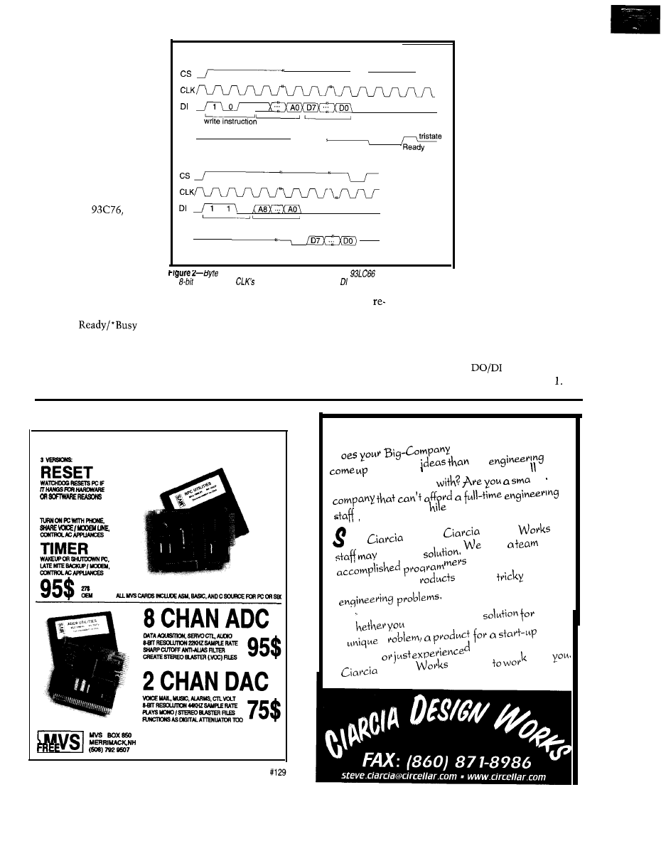
The master writes bits on
CLK’s falling edge, and the
Write (Program) Operation
EEPROM latches each bit
on the next rising edge.
After sending the final
data bit in a programming
1 \ A8
operation, the master must
address
data
bring CS low before the
DO
tristate
next rising edge of CLK.
*Busy
This action causes the
Read Operation
EEPROM to begin its inter-
nal programming cycle.
Some devices, such as
Microchip’s
don’t
0
require CS to go low here.
read instruction
address
Instead, they begin pro-
DO
tristate
gramming on CLK’s rising
0
edge after DO.
d
a
t
a
The programming is
read and write operations on a Microwire
EPROM are configured
self-timed, so it requires no
for
organization.
rising edges latch inputs at and clock data out at DO.
the EEPROM receives the
final address bit, it writes
a dummy 0 to DO and then
writes the requested data
on CLK’s rising edges.
If CS remains high after
a Read operation, extra
clock transitions cause the
chip to continue to output
data at sequential ad-
dresses. If CS goes low, the
next read operation must
begin with the Read in-
struction and an address.
A two-line interface is
sometimes possible by
connecting DO and DI.
(An isolation resistor be-
tween the lines is recom-
mended.)
clock cycles. If CS returns high before
programming session. The device
the programming cycle completes, DO
However, there is a brief bus conflict
mains write enabled until it receives an
indicates
status. CS must
in Read operations when the EEPROM
Erase/Write Disable instruction or
then go low again to complete the write
outputs the dummy zero on receiving
power is removed.
operation.
the final address bit, and the master’s
To read from the EEPROM, the
The master needs to send the Erase/
driver must be strong enough to pull
master writes a Read instruction to DI,
Write Enable instruction just once per
followed by the address to read. When
the combined
line high when
this occurs and the address bit is
REMOTE POWER CARD!
P H O N E
5 YEAR LIMITED WARRANTY
S H I P P I N G I N U S A
marketing department
the
with more
department can cope
for
o n c e - i n - a - W
designs?
teve
and the
Design
have the
have
Of
and
engineers
ready
to design p
Or solve
need an On-
line
a
p
venture,
consulting,
Design
is ready
with
68
Issue 94
July
1997
Circuit Cellar INK@
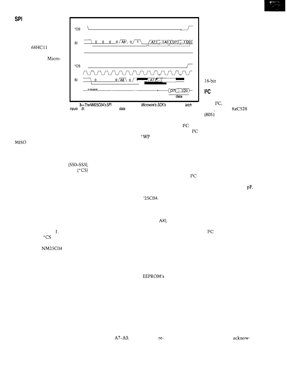
The second interface
type, SPI (Serial Peripheral
Interface), originated at
Motorola, and is included
on their
and
other microcontrollers.
SPI is much like
wire, though the signal
names, polarities, and
other details vary.
Like Microwire, SPI is
often dubbed a three-wire
interface, although a
read/write interface re-
quires two data lines, a
clock, a chip select, and a
common ground.
Write (Program) Operation
S
C
K
-
-
0
write instruction
address
data
s o
tristate
Read Operation
\
SCK
0 0
1
read instruction
address
tristate
s o
Figure
interface
is similar to
falling edges
at while rising edges clock
out on SO.
The signal names differ on the mas-
ter and slave devices. The data line
MOSI (master out, slave in) on the
master connects to SI on the slave, and
(master in, slave out) on the
master connects to SO on the slave.
The clock is called SPICK at the
master and SCK at the slave. A Master
may also have four outputs
each connecting to a chip select
on up to four slave.
As with Microwire, SPI EEPROMs
write bits on the clock’s rising edge.
But unlike Microwire, they latch input
bits on the falling edge. (The SPI proto-
col allows two different clock polari-
ties, but EEPROMs support only clock
polarity equal to 0.)
Some SPI devices support two phases
but the EEPROMs support only one
clock phase equal to Notice also that
the polarity of
is opposite from
Microwire’s convention.
National’s
is a 4-Kb
EEPROM with an SPI interface. In
addition to the four lines mentioned
above, the chip has two other inputs.
* WP must be high to program the
device. For interfaces with multiple
slaves, the *Hold input lets the master
pause in the middle of a transfer to do
something more urgent on the SPI link.
The EEPROM ignores all activity on the
SPI bus until *Hold returns high and
both devices pick up where they left off.
The EEPROM understands six in-
structions-Set and Reset the Write
Enable Latch, Read and Write to the
Status Register, and Read and Write to
the Memory Array.
70
Issue
84
July 1997
Circuit Cellar INK@
sponds with the data bits
in sequence on SO. As
with Microwire, addi-
tional clocks cause the
EEPROM to send addi-
tional data bytes in se-
quence.
For larger capacities,
rather than embedding
address bits in instruc-
tions, the master sends a
address.
The third interface
type,
originated with
Philips. Their
The chip has several levels of write
protection, which you can use to virtu-
ally guarantee there’ll be no inadvertent
writes to the device. If
is low, no
changes to the data are allowed. If it’s
high, two nonvolatile bits in the chip’s
Status Register can block writes to all
or a portion of the device.
If
l
WP is high, before you can write
to the Status Register or the portion of
memory enabled in the Status Register,
the EEPROM must receive a Set Write
Enable Latch instruction.
Figure 2 shows the timing for byte
reads and writes for the
To
write to the EEPROM, the master
writes a Set Write Enable Latch instruc-
tion to SI, followed by a Write instruc-
tion (which contains address bit
the lower eight address bits, and the
data to write.
The master may send up to four data
bytes for sequential addresses in one
operation. After clocking the final data
bit, with SCK low, CS must go high to
begin programming the byte into the
EEPROM.
While the EEPROM writes the data,
the master can read the
Status register. When bit 0 of the Status
Register is 0, the EEPROM has finished
programming and the next write can
begin. The chip is write protected after
each programming operation, so each
write must begin with a Set Write
Enable Latch instruction.
To read the EEPROM, the master
sends a Read instruction, which con-
tains bit A8 of the address to read and
then bits
The EEPROM
family) is an ex-
ample of a microcontroller with built
in
interface.
The
interface requires just two
signal lines plus a common ground.
Serial Data/Address (SDA) is a bidirec-
tional line requiring open-collector or
open-drain outputs. Serial Clock (SCL)
is the clock. Instead of a chip-select
line, the master sends a slave address
on SDA.
An
bus can have up to about 40
devices, with the limit determined by
a maximum bus capacitance of 400
Each device on the bus can have an
address of up to 7 bits.
The open-collector/open-drain inter-
face means that any logic-low output
pulls SDA low. A device releases the
SDA line by writing 1
to
its output.
Unlike Microwire and SPI, which are
edge sensitive,
is level sensitive.
Data and address bits on SDA may
change only while SCL is low, and the
receiving device reads bits after SCL
goes high.
There are two occasions when SDA
changes state while SCL is high. A
Start condition signals the beginning of
an operation and occurs when the mas-
ter brings SDA low with SCL high. A
Stop condition signals the end of an
operation and occurs when SDA goes
high with SCL high.
After most transmissions (e.g., an
instruction, address, or data byte),
during the ninth clock cycle, the trans-
mitting device releases SDA and the
receiving device pulls SDA low to
acknowledge that it received the bits.
If the master doesn’t see the
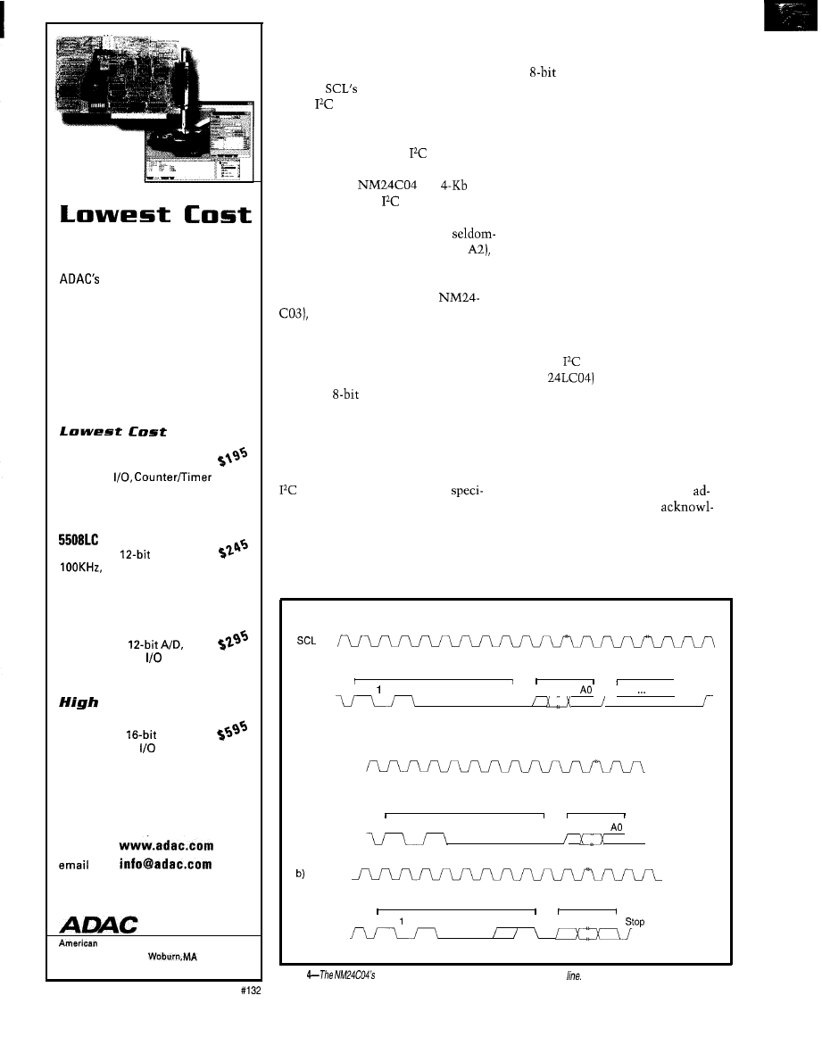
Data Acquisition
new Value-line has
uncompromising design features
and high quality components at
prices below the low cost guys!
Just check out the specs:
5500MF
8 channels 12-bit A/D,
16 digital
H i g h S p e e d
8 channels
A/D,
DMA
M u l t i - F u n c t t o n D M A
5516DMA
16 channels
DMA, 16 digital
R e s o l u t i o n
5500HR
16 channels
A/D,
DMA, 8 digital
learn more:
voice
800-648-6589
fax
617-938-6553
w e b
Data Acquisition Corporation
70 Tower Office Park,
01801 USA
ledgment, it knows something isn’t
right. The receiving device releases
SDA on
next falling edge.
An
bus can have multiple mas-
ters. If more than one master tries to
control the bus at once, an arbitration
protocol defined by the
standard
determines which one wins.
National’s
is a
EEPROM with an
interface. SDA,
SCL, power, and ground use four of the
eight pins. Three other pins are
used page-address inputs (AO,
Al,
which enable multiple low-density
EEPROMs on a single interface.
On some EEPROMs (e.g.,
the remaining pin is a hardware
write protect for the upper half of the
memory array.
The type identifier is defined by the
standard. The page address
fies address bit A8 (0 or 1). The other
two bits in the page address are unused
unless there are multiple EEPROMs.
In the clock cycle following the slave
address, the EEPROM pulls SDA low
To write a byte to the EEPROM, the
master issues a Start condition and
writes an
slave address. The ad-
dress consists of a 4-bit type identifier
(1010 for EEPROMs), followed by the
selected page (000 or 001) and a request
to read (1) or write to (0) the device.
to acknowledge. The master then sends
an
address, and the EEPROM
acknowledges. (With larger capacities,
the master can send two address bytes.)
The master sends the byte to write,
waits for an Acknowledge, and issues a
stop condition. The EEPROM then
programs the data into its memory
array. When programming is complete,
the EEPROM acknowledges.
To write to up to 16 bytes to sequen-
tial addresses, instead of issuing a Stop
condition after the first data byte, the
master may continue to send data
bytes, waiting for an Acknowledge
after each. After sending all the bytes,
the master issues the Stop condition
and the EEPROM programs the bytes
and acknowledges.
Some
EEPROMs (e.g., Micro-
chip’s
can program all 16 bytes
in parallel for much faster program-
ming. On others, you can write
16 bytes
in sequence, but the chip programs
them one at a time.
if doing a write operation, sending a
slave address followed by a byte
dress. When the EEPROM
edges the bytk address, the master
issues a new Start condition, followed
by the slave address with the final bit
set to 1 (read).
To read a byte, the master begins as
Write Operation
Master Bus activity:
write instruction
address
data
Start 0 1 0 0
0 A8 0
A7
D7 DO
S D A
stop
\ x,x \
EEPROM Bus Activity:
Ack
Ack
Ack
Read Operation
a) SCL
Master Bus activity:
dummy write instruction
address
Start 1 0 1 0
0 0 A8 0
A7 ___
SDA
\
EEPROM Bus activity:
Ack
Ack
S C L
Master Bus activity:
read instruction
data
Start 0 1 0 0
0 A8 1
S D A
EEPROM Bus activity:
Ack D7
D
O
Figure
PC interface uses a single bidirectional signal
72
Issue 94 July 1997
Circuit Cellar
INK@
The slave acknowledges, then writes
In Part 2, I’ll present the design of an
the data to SDA. On receiving the
EEPROM programmer that runs from a
data, the master doesn’t acknowledge.
PC’s parallel port with Visual Basic
Instead, it issues a Stop condition.
program code.
q
To read sequential addresses, the
master acknowledges receiving the
data byte, and the EEPROM responds
by sending the next byte in sequence.
The EEPROM continues to send bytes
until it receives a Stop condition.
Axelson is the author of
Parallel
Port Complete and The Microcontrol-
ler Idea Book. You may reach her at
or
DECISIONS
Which EEPROM should you use?
When you’re using a microcontroller
with a built-in interface or you want to
use a specific ADC in the link, the
choice is obvious.
All three types are easily available
and inexpensive. Digi-Key has 5
devices of each type for under $3 in
single quantities.
is best if you have just two signal
lines to spare or if you have a cabled
interface.
has the strongest drivers.)
If you want a clock faster than 400
choose Microwire or SPI.
For more on using serial
browse the manufacturers’ Web pages.
National Semiconductor
P.O. Box 58090
Santa Clara, CA 950528090
(408) 7215000
Fax: (408) 739-9803
www.national.com/design
68HCll
Motorola
MCU Information Line
P.O. Box 13026
Austin, TX 7871 l-3026
(5 12) 328-2268
Fax: (512) 891-4465
www.mcu.motsps.com/mc.html
Serial EEPROMs
Digi-Key Corp.
701 Brooks Ave. S
Thief Falls, MN
(218) 681-6674
Fax: (218) 681-3380
Microchip Technology, Inc.
2355 W. Chandler Blvd.
Chandler, AZ 85224-6199
(602)
Fax: (602) 786-7277
appnotes.htm
Philips Semiconductor
811 E. Arques Ave.
Sunnyvale, CA 94088-3409
(408) 9915207
Fax: (408) 991-3773
422
Very Useful
423 Moderately Useful
424 Not Useful
E-Series
EPROM FLASH SRAM
emulation
and LIVE editing, 1 to 8 Mbit,
70 ns access time. 3V options.
S c a n l o n D e s i g n I n c .
Tel (902) 425 3938 Fax (902) 425 4098
S a l e s
I n f o ( 8 0 0 ) 3 5 2 9 7 7 0
Circuit Cellar INK@
Issue 84 July 1997
73
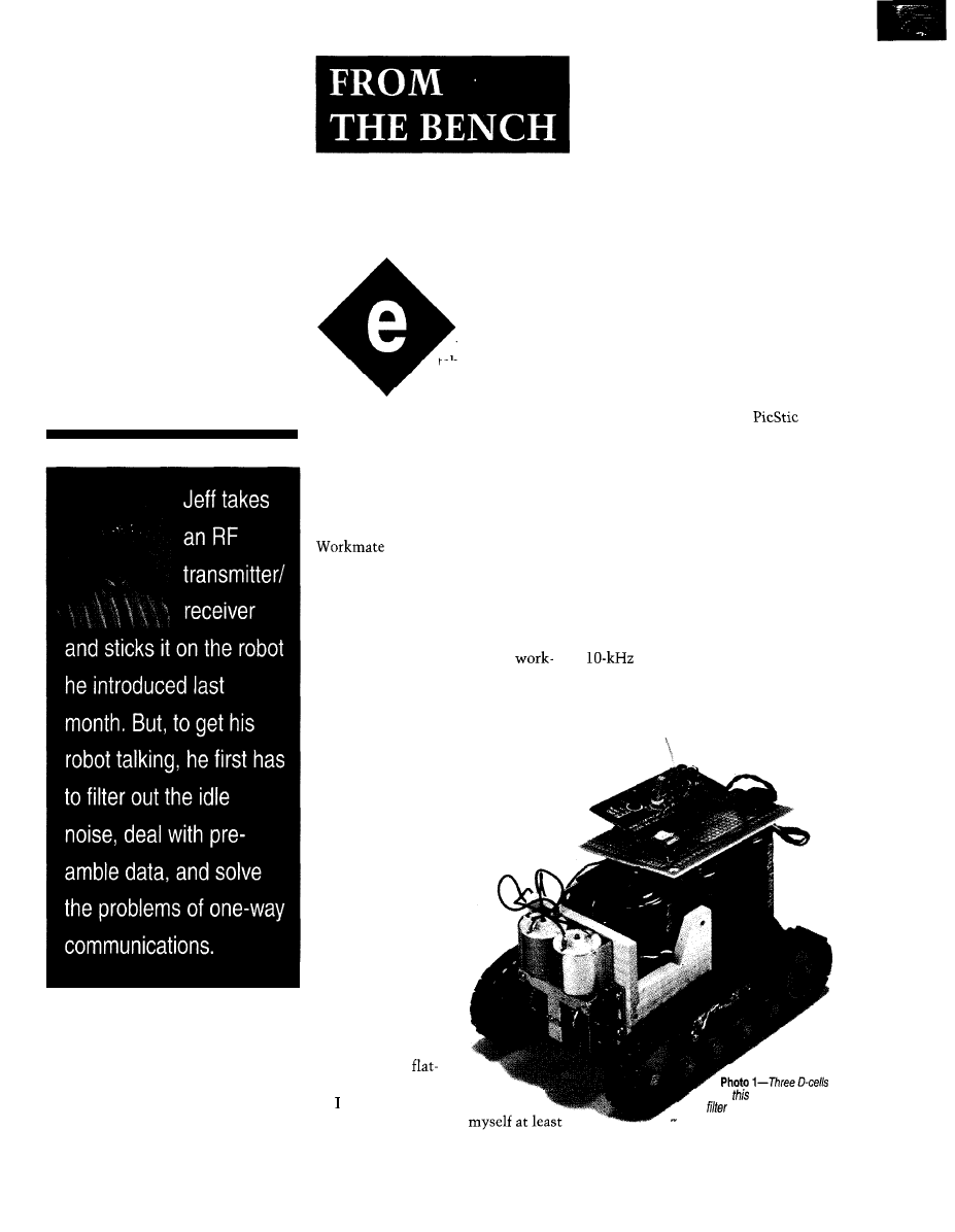
It Can’t Be
A Robot
Jeff Bachiochi
Part 2:
It Doesn’t Talk
7 4
Issue 84 July 1997
Circuit Cellar INK@
very project
takes much longer
to complete than you
anticipate. At least, that’s
what Murphy claims. And, my experi-
ence backs it up.
It started with my wife Beverly
standing before me holding a deformed
picture frame. Her “Can you fix it?”
launched a thousand ships.
I assumed the Black and Decker
could clamp the frame
squarely while the glue set. But, I no-
ticed it was wobbly. A bolt had worked
its way loose and was now lost.
After searching for another bolt for
a good 15 minutes, my best match was
a bit too big for the hole in the
mate. I decided to open the hole so I
could use the scavenged hardware.
Although the reversible drill was
handy, it took me a few minutes to
find the chuck. Once found and the bit
tightened, I squeezed the trigger.
Nothing. Fatigue had reared its
ugly head. The plug was gone.
Did I have a spare plug? You
bet. However, it needed to be
detached from an old lamp.
With a flat-bladed
screwdriver, I loosened
its screws and tried to
attach it to the drill’s
cord. But, the screws
wouldn’t tighten. The
shaft of the screw-
driver was spinning
in the handle. And, of
course, I couldn’t
locate another
blade screwdriver.
could have fixed th
handle (and guaranteed
e
loose
5 minutes of free time while the epoxy
dried), but too many higher priority
interrupts were overflowing my stack.
So, with a pair of vice grips, I grabbed
the flat-blade screwdriver by the shaft
and tightened the screws.
DETOUR
Similarly, this month, I intended to
quickly show you how to add an inex-
pensive RF transmitter/receiver pair to
the robotic platform I introduced last
month (see Photo 1, INK 83).
But, when I examined the receiver’s
output, it contained random nqise
while no carrier was being transmitted.
Although a hardware UART rejects
data that doesn’t follow bit-timing
minimums and maximums, a software
UART like the one in the
is
more likely to accept any noise as data.
I needed to filter out as much noise
as possible. So, I started by looking at
what changing carrier rates were ac-
ceptable to the receiver. I used a signal
generator to gate the transmitter on
and off. Figure 1 shows my test results.
The receiver couldn’t stay locked
whenever the carrier was modulated
slower than -10 Hz (this explained the
noise I was seeing). Also, at the high
end, it had trouble slewing above a
modulation rate.
It looked as though I might be able
to squeak through data rates of up to
9600. To prevent extraneous noise
power
robotic platform.
The
and RF receiver are
mounted atop the platform.
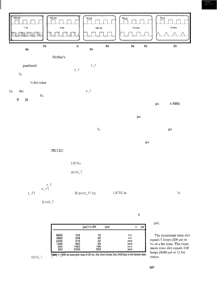
Figure l--The upper traces show frequency generator’s input the RF transmitter, while lower traces indicate output of RF receiver. Notice how noise
increases when modulation is slow and how the signal’s slew rate is limited at high end.
from creating havoc with the
software UART, I wanted to create as
narrow a
as possible.
is 0. Otherwise, the l-state counter is
cleared.
To be safe, I chose a minimum time
slot of a bit time and a maximum
time slot of 12 bit times. When data
transmits, the
minimum
assures that worst-case data (alternating
and passes without interference.
Finally, 1 a s
1 a g
is
updated with
i
1 a g in preparation for the next
sample. The timer is polled for an over-
flow (there are no interrupts here] before
beginning a new sample.
C N
T Rx
is now incremented but held
at a maximum of 255. Finally, the timer
is polled for an overflow (no interrupts
here) before beginning a new sample.
TIME TRIALS
On data that’s all there are at
least bits data bits and a stop bit)
in which the carrier doesn’t change
(plus the intercharacter spacing), hence
the choice of 12 bit times as a maxi-
mum time slot.
If no change of state is detected,
checking i
1 a g routes the program
flow to one of two identical routines.
A 0 steers the flow into the O-state
routine, and a 1 jumps to the l-state
routine.
Up to now, everything was done
without knowing the exact execution
times and thus the maximum serial
data rate (throughput). The longest
execution path for this code requires
35 cycles or 35 with a
inter-
nal clock. Now for some calculations.
My challenge: to do the filtering
digitally by using a micro with few-or
better yet, absolutely no-external
components. By sampling the incoming
data -10 times per bit time, I hoped to
reduce the phase and resolution error
as much as practically possible. (The
internal RC oscillator of the
508 I planned to use for the filter has
about 10% accuracy over voltage and
temperature.)
These program paths check to see
how long the sampled data has been
unchanged. If my specifications call for
10 samples per bit time and the mini-
mum time slot is bit, then the mini-
mum number of consecutive samples
must be 5 to be considered good.
At 4 MHz, the routine takes at least
35 to execute. Table 1 shows that
2400 bps is the fastest rate the routine
can handle and still have time to com-
plete [that’s with only 7 to spare).
At the other end, the maximum
time slot is
12
bit times. Therefore,
the maximum samples must be 120
(10 x 12 bits) to be considered good.
Since the timer has no interrupt, it
must be polled. The polling loop re-
quires 4 to execute (i.e., grab the
timer count, test for zero, and if neces-
sary, jump back to poll again).
The pseudocode in Listing 1 shows
my thought process for this digital
filter. At the beginning of each sample,
a timer is set and the input data is
sampled and stored as the
i
1 a g
bit. By comparing the
i
a g
bit
with the 1 a s
a g
bit, a potential
change of state can be determined.
If the consecutive sample counter
(where x = 0 for O-state and 1
for I-state) is within the good range,
1 ag
is set. Otherwise, it is
cleared. (This flag was checked in the
change-of-state routine to determine
whether to clear or increment the
good-bit counter
CNTRG.)
After the timer is grabbed, it contin-
ues to count during the next three
instructions. It could pass through zero
while one instruction executes if the
timer doesn’t have a prescale divisor.
If a change took place,
1 a g
is checked. This flag indicates whether
the last logic state was completed
within the time slot allotted.
If it was good, a good-bit counter is
isset,then
compared to the value 8 (an arbitrary
value), which indicates the number of
consecutive good bits that must be
received before the carrier detect out-
put is set and the input data is allowed
to pass through the filter.
Choose divide by 4 to ensure the
timer remains at each count for those
four instruction cycles of the loop.
Therefore, the timer should be reloaded
with a number that’s actually of the
count you’re looking for.
Now, we know what to expect from
the filter and can fill in a few blanks. If
the loop time set by the timer is to be
-42 (actually since it must be divisible
by 4, we need to choose either 40 or
incremented (but pre-
vented from exceeding
255). If it was bad, the
good-bit counter is cleared
along with the data output
bit and the carrier-detect
output bit.
44
the minimum and
Baud Rate Bit Time
Time
Execution Loop 35
maximum number of loops
19200
52
5
n o
necessary can be defined.
Next, the O-state coun-
ter is cleared if
n
rate this filter can accept.
Circuit Cellar
Issue 84 July 1997
7 5
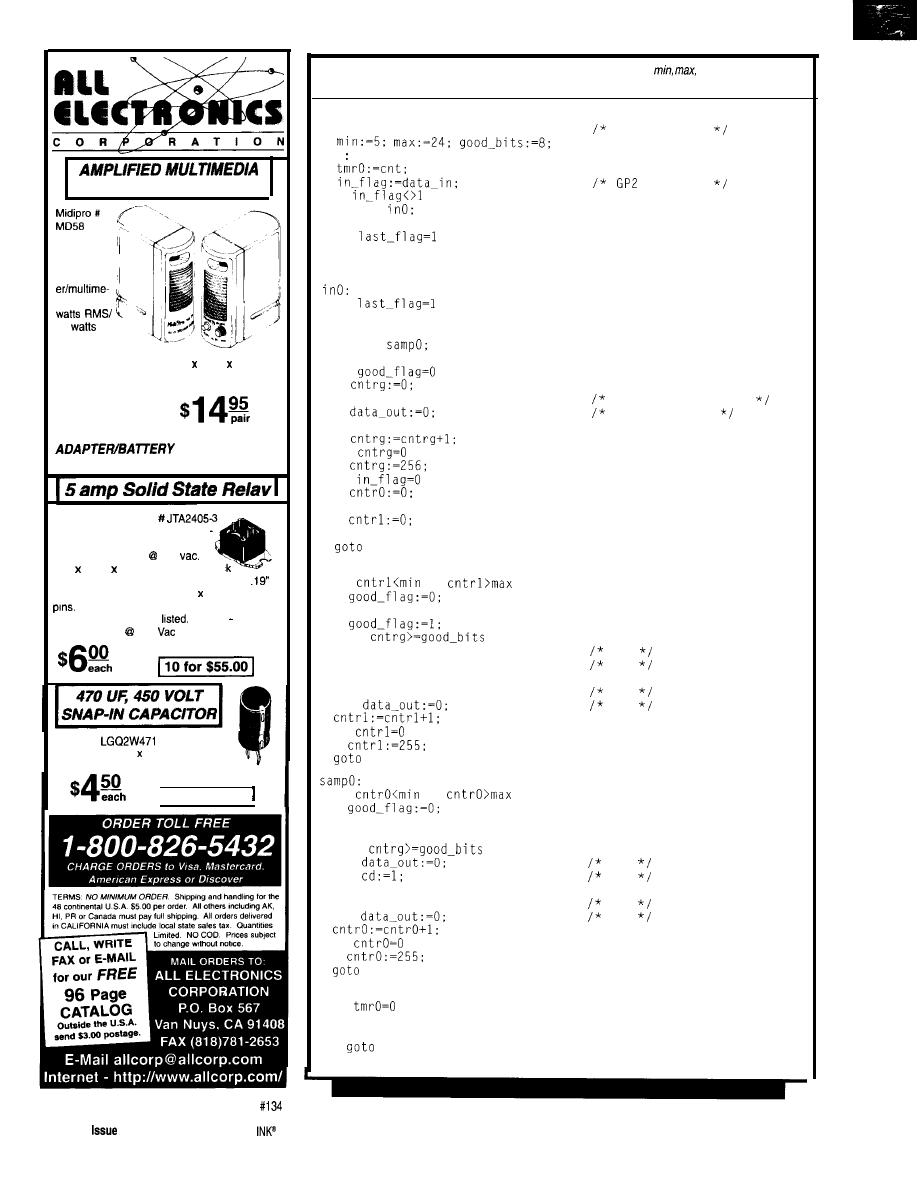
SPEAKERS
A m p l i f i e d
stereo
s p e a k e r s
for comput-
dia use. 3
12
peak
full range 8 ohm
speakers. Beige cabinets, port-
ed for extra response. 7.24” 2.95” 4.75”.
Operates on 6 volts. Includes cables. Requires
either 4 C cell batteries or 6 to 12 volt power
adapter (not Included).
CAT # SK-58
Above speaker set including DC POWER
ELIMINATOR
CAT# SK-58A $17.95
per
set
C.P. CLARE /Theta J
Compact, TTL compatible, optical
ly isolated solid state relay for
loads up to 5 amps 240
0.8” 0.82” 0.56” high epoxy bloc
with a 1.4” long metal mounting flange. 1
mounting centers. 0.062” dia. 0.175” high
Pins can be pc mounted wrapped and
soldered UL and CSA
Input: 4 8 Vdc
Load: 5 amps 240
CAT# SSRLY-2405
Nichicon
MHSC
1.375” diameter 2” high. 0.4” lead
spacing.
CAT# EC-4745
I
10 for $40.00
Listing l--Here’s
pseudo code showing data sampling and comparisons of
and good bits for a
legal output.
b e g i n
i n i t i a l i z e c h i p ;
1 cnt = 42 us
top
( D a t a i n )
i f
t h e n
got0
inl:
if
then
got0 sampl;
else
got0 cos:
if
then
got0 cos;
else
got0
cos:
if
then
cd:=O;
GP5 (CD output LED)
GP4 (Data out)
else
if
then
if
then
else
last_flag:=in_flag
bottom:
sampl:
if
or
then
else
if
then
data_out:=l;
GP4
cd:=l;
GP5
else
cd:=O;
GP5
GP4
if
then
bottom:
if
or
then
else
good_flag:=l:
if
then
GP4
GP5
else
cd:=O;
GP5
GP4
if
then
bottom:
bottom:
if
then
got0 top
else
bottom
end
76
84
July 1997
Circuit Cellar
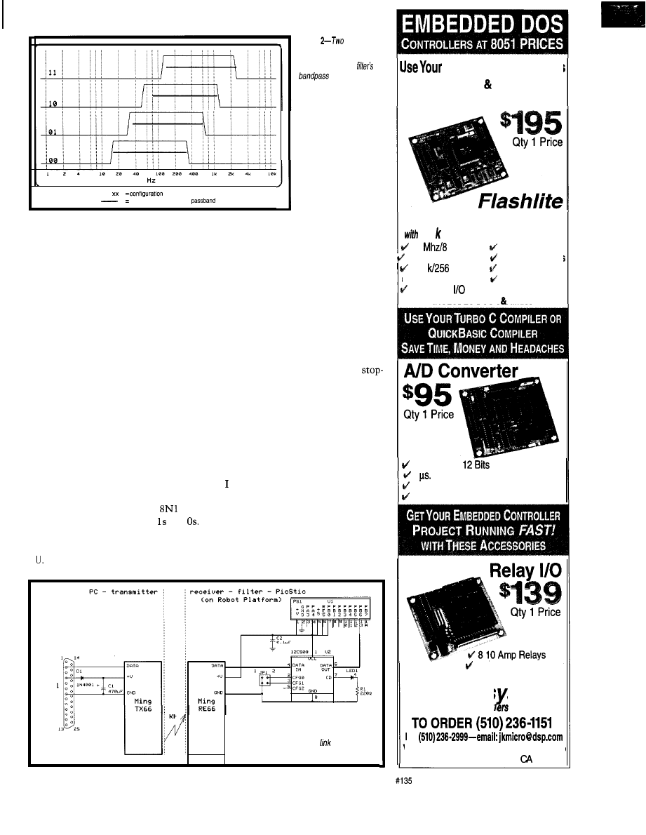
jumper
minimum to maximum
By simply changing the timer reload
value, the execution loop can be in-
creased. Spare input pins let the user
select one of four possible reload values,
adjusting the filter to pass either 300,
600, 1200, or 2400 bps.
Again, using the frequency generator,
I ran test inputs through the filter. The
results are in Figure 2.
PREAMBLE
Transmission of data presumes a few
things. First, it takes 8 good bits (an
arbitrary number] before anything
passes through the filter. This isn’t a
problem since the receiver requires a
certain time to get synced-up.
Some kind of preamble data wakes
up the filter and the receiver’s front
end. If some of the first transmitted bits
are lost, how can we know the UART
will sync up on a true start bit?
Sending capital
Us
using an
data
format looks like a stream of and
No matter where a UART starts receiv-
ing data, it will look like it’s receiving
a
Figure
configura-
tion bits choose different
timer reload values, thereby
shifting this digital
region.
If these
Us
are
followed by a char-
acter 2 5 5 (the sync
character), the
UART will finish a
byte sometime
during this character, and there’s only
a small chance it will be a
U.
Since there will be no additional bit
transitions during this character, the
UART will be ready for a new start bit
when the actual data begins immedi-
ately following this sync character.
So at the transmission end, a few
extra bytes of data must be appended
to each new message transmitted (a new
message consists of any transmission
which begins after more than one
bit delay).
At the receiving end, the UART
reception is ignored until an
M is re-
ceived (i.e., the first legal character in a
command). So, the preamble is essen-
tially invisible.
RETURN FROM INTERRUPT
think we’re about back to where I
expected to be at the beginning of this
article-cutting the robot’s umbilical
cord without giving it much of a pur-
pose in life.
A Ming transmitter/receiver pair
works nicely (once this month’s filter
PC’S
s e r i a l
p o r t
Figure 3-A one-way RF
lets Logo-type
commands control the
robotic platform.
PC Development Tools
No
M
ORE
C
RASH
B
URN
EPROM
Technology
DOS Single Board Computer
572
FLASH
Memory disk drive
10
Mhz CPU 2 Timers
512 k bytes RAM
4 Interrupt Line:
512
k FLASH 8 Analog Inputs
4 2 Serial Ports
X-Modem File
24 Parallel Lines
Transfer
INCLUDES DOS
Utilities
8 Channels,
6 Conversion Time
Clock/Calendar Option
Includes Drivers & Apps.
8 Opto-Isolated Inputs
JK micros stems
Cost Effective Control for industry
FAX
Visit our
WEB
site-www.dsp.com/jkmicro
1275 Yuba Ave., San Pablo,
94806
Circuit Cellar INK@
Issue 94 July 1997
7 7
8051 Family Emulator is
truly Low Cost!
The
Plus is a
modular emulator
designed to get maximum flexibility
and functionality for
your hard earned
dollar.
The common base unit
supports numerous
805
1
family
processor
pods that are low in price.
Features
include:
Execute to
breakpoint, Line-by-Line Assembler,
Disassembler, SFR access, Fill, Set
and Dump Internal or External RAM
and Code, Dump Registers, and
more. The
Flus base unit is
priced at a meager $299, and most
pods run only an
$149.
Pods are available to support the
803
1,
1 ,
and more. Interface through
your serial port and a
program.
Call for a brochure or use INTERNET.
We’re at
o r
www.hte.com.
Our $149
model is what
you’re looking for.
Not an evaluation
board much more powerful. Same
features as the
but limited
to just the
processor.
So, if you’re still doing the
U V
Waltz (Burn-2-3, Erase-2-3). or
debugging through the
window
ROM emulators give,
us
Our customers say our products
are
b e s t
emulators available!
Equipment Corp.
S i n c e 1 9 8 3
(619) 566-l 892
Internet e-mail: info@hte.com
World Wide Web:
www.hte.com
Choose Command
A=add step to program
V=view program steps
E=edit program steps
C=clear program steps
P=play program steps
a program to a file
G=get a program file
X=exit program
Viewing program steps
1
10
2
MR 45
3
MF 10
4
MR 45
5
10
6
MR 45
7
MF 10
8
MR 45
9
MF 10
10
MR 45
11
MF 10
12
MR 45
13
10
14
MR 45
15
MF 10
16 MR 45
Finished
Figure 4-A logo-sty/e program
written in
the
platform execute a number
steps or functions (i.e., move forward
is added to get rid of the idle noise) for
sending commands to the platform
using RF (see Figure 3).
It led me to write a GWBASIC pro-
gram on my PC that enables a routine
of commands to be entered, listed,
edited, saved to a file, loaded from a
file, and sent to the robot over the RF
link. The robot becomes a Logo type
operator as shown in Figure 4.
I showed four robot commands last
month-Forward, Backward, Left Turn,
and Right Turn. My program lets the
user choose any of these and prompts
for a distance in inches or degrees.
Through trial runs, I determined the
actual motions and added multiplier
constants for the distance and degrees.
It’s more user friendly than asking for
the distance and direction in units.
You can add commands to create a
lengthy repertoire of actions. Since the
program lets you save and retrieve, you
can use a simple text editor to create a
movement command list.
There is a potential problem with
one-way communications. There’s
always the possibility that a command
could be jumbled or lost, and you’d
never know it until the robot crashes
into something unexpected.
With the umbilical cord, there was
an echo of the command--the hand-
shaking--to assure you the command
was done. This isn’t possible with
only one transmitter and one receiver.
So, again I needed to add a multiplier
constant. This time, and I do mean
time, I needed a way to pause between
commands just long enough to be sure
the last command had completed.
I used the number entered either for
distance or degrees and multiplied it
by the constant to get a pause duration
in fractions of a second. The BASIC
T i me r
command let me easily and
accurately wait an appropriate time,
based directly on how far the platform
was going to move.
LIFE BEYOND THE KEYBOARD
If I can pry this little robot away
from my kids long enough, I’ll add
some sensors next month. Supposing
this thing is ever to roam on its own, I
need to add some collision avoidance.
Speaking of collision avoidance,
maybe I should design some for the
picture too since that’s how it got
broken. Perhaps its glue is dry by now.
Time to get it back on the wall.
q
Jeff Bachiochi (pronounced
is an
electrical
engineer on
Circuit Cellar INK’s engineering
staff.
His background includes product
design and manufacturing. He may be
reached at
corn.
Microchip Technology, Inc.
2355 W. Chandler Blvd.
Chandler, AZ 85224-6199
(602) 786-7200
Fax: (602) 786-7277
www.microchip.com
Ming-RX66 transmitter
and
receiver
Digi-Key Corp.
701 Brooks Ave.
Thief Falls, MN
(218) 681-6674
Fax: (218) 681-3380
425
Very Useful
426 Moderately Useful
427 Not Useful
78
Issue
84 July 1997
Circuit Cellar INK@
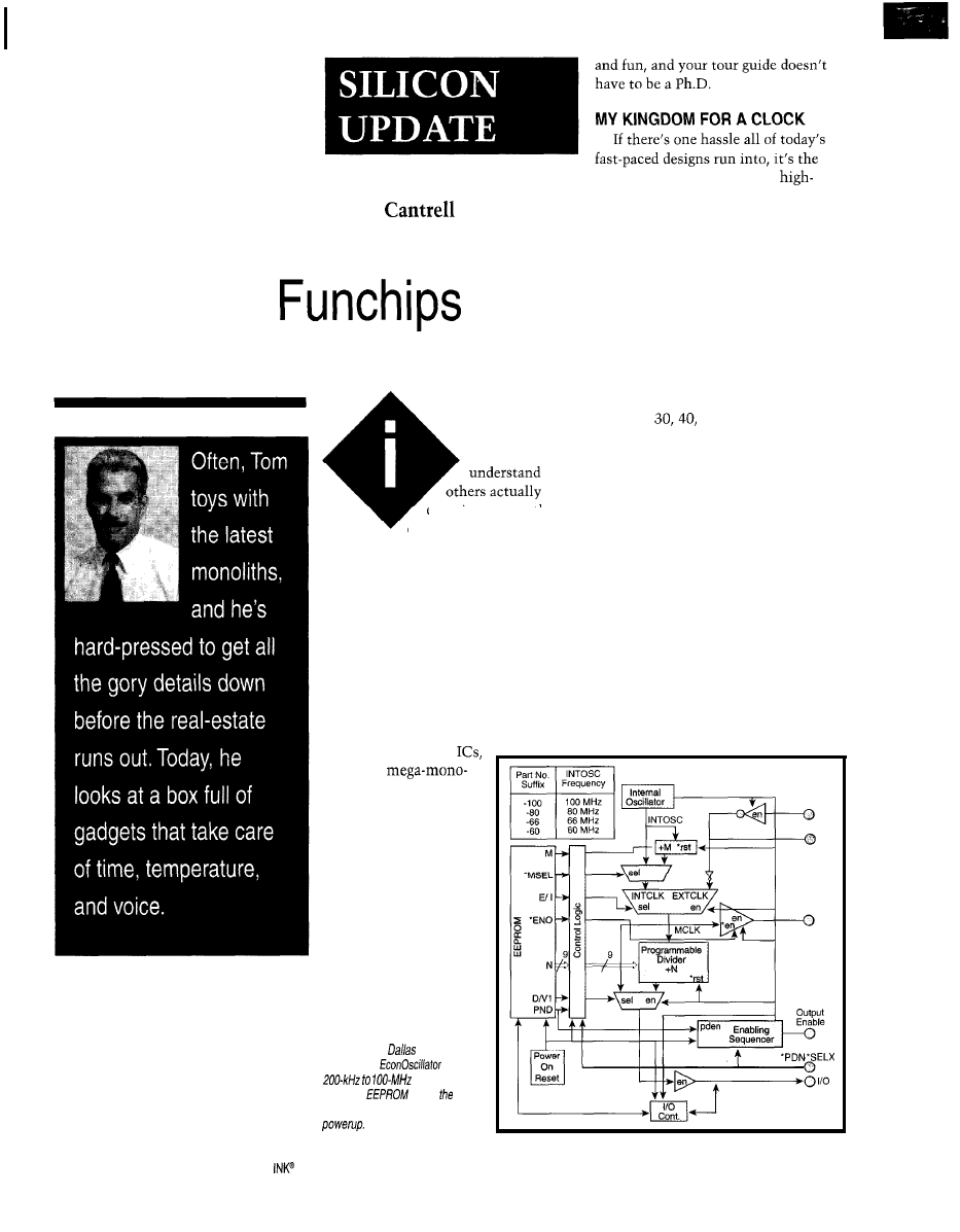
need to generate and control
Tom
speed clocks.
Traditional embedded setups run-
ning at O-20 MHz or so have had it
easy. This range is where the ubiquitous
fundamental overtone crystal rules and
Cruise the
80
Issue
84 July 1997
Circuit Cellar
experience something
called “vacations.” I’m not
one of ‘em, though you could argue my
entire life qualifies since I enjoy my
work. If I was an MIS administrator or
insurance salesman, it might be another
story.
From way back when, one approach
has been to extract an overtone of the
fundamental crystal. Unfortunately, it
seems there are just too many start-up
and reliability problems.
I’m not enough of an expert on oscil-
lator design (a rather black art) to know
There seem to be two schools of
thought when it comes to vacations.
One is to try to pack as many locations
exactly why this is the case. But, you
and sights as possible into a whirlwind
don’t have to be a guru to understand
tour. The other is to go bury your head
that if the overtone trick worked, its
in the sand on a beach somewhere.
use would be much more widespread.
When it comes to
manufacturers have really got their
oscillator designs perfected.
Short of adding a couple of caps and
obeying common-sense layout rules,
there’s little hassle for the designer.
Wire it up, and it works.
Ah, but what if your system needs a
rev-up to
50 MHz and beyond?
Turns out, it’s tough to fabricate such
high-speed fundamental crystals-at
least ones that aren’t ridiculously
fragile. A number of alternatives have
emerged over the years, but all of them
come with irritating consequences.
the latest
lith microchips are so
complicated, it’s easy to
get a headache just trying
to explain them. Like
the overcaffeinated vaca-
tion, there’s so much
ground to cover, you
can’t enjoy the sights.
So, why don’t we take
a nice calming cruise on
the Funchips? These
gadgets are economical
Figure l--The
Semiconduc-
tor DS107.5
is a
clocking
solution.
stores divide
ratios for automatic operation at
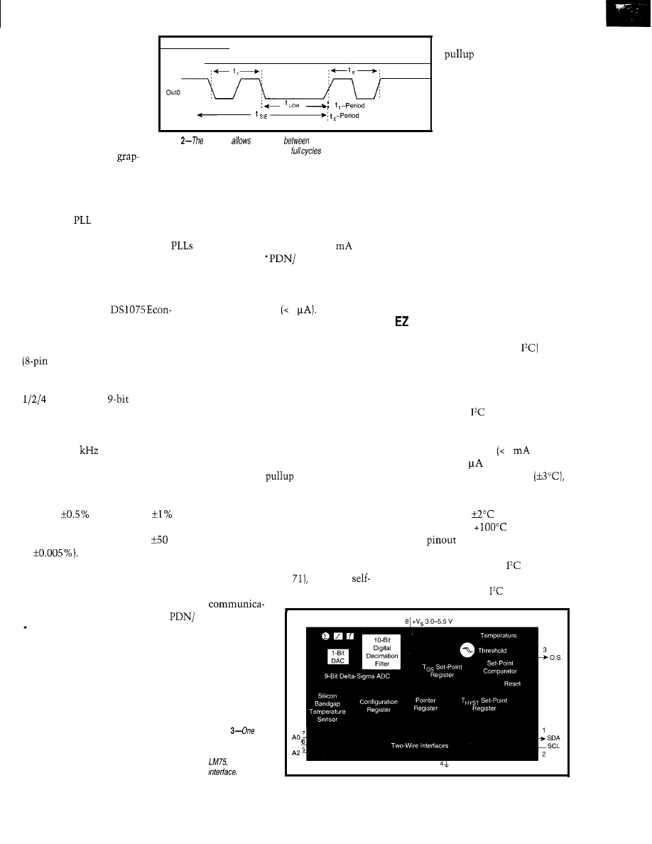
Instead, most designers
just punt and design in the
stalwart DIP-can hybrid-TTL
oscillator. These devices are
OK, but they’re pricey,
bulky, and high power. The
simplest ones also lack any
means of controlling the
clock, short of switching
power on and off and
‘ S E L X \
\
of Internal Clock
of External Clock
Figure
DS107.5
switching
external and internal clocks. The
output is he/d low during the transition, and
on both sides are guaranteed.
pling with the resulting glitches.
From a system designer’s perspec-
tive, the best thing to do is fingerpoint
the chip designer and demand they
design in a
clock multiplier. While
they’re at it, tell ‘em to make sure it
can be turned off (high-frequency
use a lot of power) yet lock up real
quick when called into action. Of
course, it would be nice if they didn’t
increase the chip’s price either.
Enter the Dallas
Oscillator. It handles high-frequency
clocking with quite a bit of panache.
As shown in Figure 1, this puppy
DIP or SOIC package) starts with
a fixed rate (60, 66, 80, or 100 MHz)
internal oscillator feeding a divide by
prescaler and
divider.
That works out to 1536 different
choices (though many overlap), cover-
ing a range from 100 MHz all the way
down to 200
(the specified mini-
mum output frequency). Between the
four speed grades, prescaler, and divider,
it should be possible to come quite
close to the frequency you need. Do
note the
accuracy and
temp variation isn’t as good as a crys-
tal oscillator (typically about
ppm
or
If all the choices on chip aren’t
enough, the chip also accommodates
an external clock input-either TTL
on the OSCIN pin or a crystal between
OSCIN and XTAL. Assuming the
SELX pin is configured for the * SELX
(select) function, it can be used to
switch dynamically between the inter-
nal and external timebases.
Notably, the switch is glitchless (the
primary output, IN/OUT, is held low
during the changeover) as you see in
Figure 2. A secondary output, OUTO,
grabs the output of the internal/exter-
nal selection mux.
The ‘1075 also features an OE (out-
put enable) pin that uses similar enable
The need to power cycle
the chip and the dual use of
the single pin as both a
programming port and the
clock out hinder self-clock-
ing schemes.
and disable sequencing to eliminate
any truncated clocks or variable phas-
ing (i.e., the divider chain is reset by
OE transitions). Note that OE controls
Though drawing up to 50
when
running, the
l
SELX pin invokes
power-down mode. This action shuts
the main (IN/OUT), but not the sec-
off the oscillator and both clock out-
puts, thereby cutting power consump-
ondary (OUTO), clock output.
tion to the bone 1
For instance, it would be neat if the
chip relied on EEPROM to boot up a
micro at a default clock rate but then
Putting aside wild and crazy ideas (at
allowed the micro to dynamically
least for now), it seems clear the high
speed and configurability of the DS 1750
means it’s something a well-traveled
change it (admittedly, a scheme fraught
designer shouldn’t forget to pack.
with risk, but intriguing nevertheless).
There are a couple compromises
that come with the package. In other
words, eight pins don’t go a long way.
TEMP
While internal/external selection,
output enabling, and powerdown are
all intended for dynamic operation, the
actual divide ratios aren’t. Instead,
they and other key mode selections
(e.g., which function the
l
PDN/*SELX
pin performs) are preprogrammed into
EEPROM for no-programming startup.
Another chip with a wire-miser
serial interface (in this case,
is the
National LM75 digital temperature
sensor. As depicted in Figure 3, the
chip combines a raw temp sensor,
signal conditioning, ADC, set-point
comparator, and
interface in its
tiny S-pin SOP package.
Programming is accomplished by
connecting a
to the IN/OUT pin.
When power is applied, the chip detects
the high input as a signal to use the
IN/OUT pin for programming rather
than as the primary clock output.
Key specs include 3.0-5.5-V opera-
tion and low operating 1
typical)
and quiescent (1
typical) currents.
As well, it has decent accuracy
considering the very wide temperature
range of -55” to 125°C. Indeed, accu-
racy improves to
over the more
temperate -25” to
range.
The programming scheme itself is
based on the unique Dallas one-wire
LAN protocol (see “The Little LAN
That Could,” INK
in which
timed devices achieve bidirectional
The
is blessedly simple.
There’s power (3-5.5 V) and ground, the
two-wire (SDA and SCL)
interface,
three address lines specifying the least
significant bits of the
address (i.e.,
power must be removed, the
disconnected, and
power restored for any
changes to take effect.
tion over a
single wire.
Once the divide
and mode bits
are written.
Figure
of the
most recent digital
Al
temp sensors, the
features an PC
Circuit Cellar INK@
Issue 84 July 1997
81
up to eight
can be con-
nected), and an overtemperature
shutdown (OS) output.
This output can be program-
med to operate in either compar-
ator or interrupt mode. Figure 4
illustrates how the former is like
a typical thermostat, in which
the output directly reflects the
comparison result subject to
programmed hysteresis.
By contrast, interrupt mode
generates a pulse (programmably
low or high) on each comparator
transition. The interrupt is
Mode)
Temperature response shown for
set
Time
burying your nose in a maga-
zine, putting on headphones,
or speaking a foreign language
seem to blow right by those
determined to chat.
Better hope it’s not a long
trip if the TriTech TR83
voice storage controller (see
Figure 6) plops down next to
you. Handling up to 14 min. of
speech, this chip can talk your
head off.
Figure
OS
Shutdown) pin can be programmed
in either comparator (i.e., thermostat) or interrupt mode.
Easy-to-use, not to mention reason-
ably priced ($1.59 in 100s) digital temp
chips like the LM75 inspire a few mo-
ments of nostalgia for the good old days
of diodes and op-amps.
Oops, no time to mourn. There’s
one more stop on our cruise.
BLABBER CHIP
Ever get stuck on a plane, train, or
automobile next to somebody who just
wouldn’t shut up? Subtle hints like
Of course, another strategy
for dealing with a
who won’t shut up is to drink
until either what they’re say-
ing sounds interesting or, better yet,
you feel like sharing your own story.
Fortunately, the TR83
is a
good listener as well (i.e., it’s both a
recorder and player). It’s quite similar
in concept to the single-chip solutions
from ISD (see “Talking Chips,” INK
36) except storage capacity is much
higher, thanks to the TriTech chip’s
reliance on external flash memory.
Wiring the ‘83 100 starts with con-
necting a crystal (20 MHz), microphone
cleared by reading any of the
four on-chip registers or placing the
LM75 in low-power shutdown mode.
The OS output is open collector
without an internal
enabling it
to be
with other active-low
sources. The datasheet cautions to use
a weak (e.g., 30
to minimize
self-heating. Remember, the most
direct thermal connection is from die
to pins to PCB.
To minimize
address consump-
tion, the LM75 is programmed via a
single pointer register that directs
access to the temperature, setpoint,
hysteresis, and configuration registers
as shown in Figure 5.
The configuration register controls
the previously mentioned features
(i.e., low-power shutdown, compare and
interrupt modes, and OS pin polarity).
In addition, two fault-queue bits func-
tion as a low-pass filter by specifying
that 1, 2, 4, or 8 consecutive samples
must pass inspection before allowing
an OS transition.
There’s no need to explore the de-
tails of
since it’s been well covered
in INK and elsewhere. The LM75 is an
slave (i.e., the host provides the
clock). Do note that the pointer and
configuration registers are 8 bits wide,
while the temp, setpoint, and hyster-
esis registers are 16 bits wide.
Watch out for inadvertently trying
to perform an
read from a 16-bit
register. If D7 (i.e., the ninth bit shifted)
is 0, things can deadlock with both the
CPU and LM75 waiting for the other
to do something.
The
requires the CPU to issue
nine additional clocks to get things
back in sync.
of the code. M. Ryan
“We
p l e a s e d w i t h t h e
General Software BIOS and look
Instant Boot, Console Redirection, Much More
forward working with you to bring
our product market.
Expert Support with Guaranteed Response Time
Embedded BIOS is well-structured
We Work Closely With
AMD, Intel,
and documented, and technical
to Deliver you a Proven, Tested, Feature-Packed BIOS
General
is
excellent.
of Units Already Licensed
am sure
made the right
decision buy our BIOS from
BIOS
Kit Includes:
General Software.”
Complete Source Code
“Embedded
is really
Binary Configuration Program
General Software, Inc.
3 2 0 1 0 8 t h A v e . N . E . . S u i t e 4 0 0
W A 9 8 0 0 4
T e l : 2 0 6 . 4 5 4 . 5 7 5 5 . F a x : 2 0 6 . 4 5 4 . 5 7 4 4
S a l e s :
E - M a i l :
Circuit Cellar
Issue 84 July 1997
83
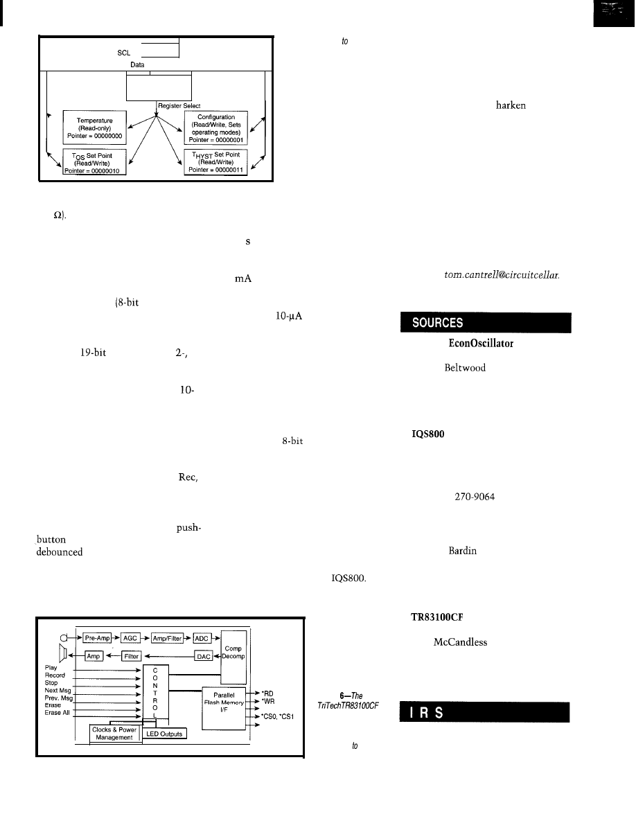
SDA
Interface
Address
Pointer Register
(Selects register for
Communication)
(electret, AC coupled), and speaker
(32 The analog section includes
practically everything (i.e., amps, AGC,
and converters), though the active
filter (shared between input and out-
put) requires tuning with a handful of
external Rs and Cs.
The ‘83 100 direct connects to a
variety of parallel
data) flash
chips. Up to two memory chips can be
used (i.e., two chip-select pins), but
both must be of the same type.
With a
address bus, l-, and
4-Mb flash chips are supported, so the
maximum storage is 8 Mb [i.e., two
512 K x 8 chips). With selectable
or
20-kbps ADPCM compression, that
translates to 14 or 7 min., respectively.
Like other chips used in digital
answering machines, cellular phones,
toys, and voice memo gadgets, the
‘83100 features a rather self-explanatory
push-button interface [e.g., Play,
etc.). There are also a couple LED out-
puts giving operationalfeedback (e.g.,
LED2 goes on during recording).
Since the unit is intended for
use, the inputs are not only
(30 ms), but they perform
special functions when held. So, if you
push the Next button during playback,
it goes to the next message, but if you
hold it down for more than 0.5 s, it
Figure B-Access the four
LM75 on-chip control registers is
via a pointer register.
plays back the current message fast
(150%) until released. Similarly, the
Erase and Erase All inputs require 0.5
and 1 of convincing, respectively,
before they do their dirty deeds.
Power consumption during playback
(77
typical at 5 V) is dominated by
the amplifier. However, when otherwise
not busy for 3 s, the ‘83100 automati-
cally enters a
power-down mode.
A falling edge on any of the button
inputs automatically awakens the chip
and executes the appropriate command,
making powerdown completely trans-
parent to the user.
Naturally, it’s no problem to coerce
a micro into dealing with the ‘83 100
push-button interface. However, the
company mentions that since the chip
is based on an
micro, they can
modify it (e.g., with a serial interface)
for different applications.
As it stands, the ‘83100 is really best
suited for push-button-based designs.
Keep in mind that there’s no way to
directly access a particular message out
of order or string arbitrary sequences
together.
If you just need a playback-only chip
with a more micro-accessible interface,
check out the IQ Systems
Other than lacking the record feature
(audio data is prepared ahead of time
ADDR (C-18)
DATA (O-7)
Figure
is
a voice recorder that
works with standard
external
f/ash chips to
provide
up
14 min.
of storage.
on a PC), it’s otherwise quite similar
to the TriTech chip.
BACK TO REALITY
I look forward to more relaxing
visits with chips that
from a
simpler time. Nothing like a vacation
to recharge the old batteries.
But, back home in Silicon Valley,
things move at a faster pace. Refreshed
by the R&R, I’m a little better pre-
pared to deal with the next zillion
transistor wunderchips that come
down the pike. Bring ‘em on!
q
Tom Cantrell has been working on
chip, board, and systems design and
marketing in Silicon Valley for more
than ten years. He may be reached by
E-mail at
corn, by telephone at (510) 657-0264,
or by fax at (510) 657-5441.
DS1075
Dallas Semiconductor
4401 S.
Pkwy.
Dallas, TX 75244-3292
(214) 778-6824
Fax: (214) 778-6004
www.dalsemi.com
IQ Systems, Inc.
75 Glen Rd.
Sandy Hook, CT 06482
(203) 270-9064
Fax: (203)
www.iqsystemsinc.com
LM75
National Semiconductor Corp.
1111 W.
Rd.
Arlington, TX 76017
(408) 721-5000
Fax: (817) 468-6935
www.national.com
Tritech Microelectronics Intl.
1400
Dr.
Milpitas, CA 95025-1900
(408) 894-1900
Fax: (408) 941-1301
www.tritech-sg.com
428 Very Useful
429 Moderately Useful
430 Not Useful
84
Issue
94 July 1997
Circuit Cellar INK@
INTERRUPT
Don’t Lose Your Head
hile certainly don’t think executions are anything to joke about, there is a gag about the French Revolution
has a message buried in the humor. Perhaps you’ve heard the one about the engineer and the guillotine?
Apparently, a number of different professionals were about to be executed. A lawyer was led up the stairs and
that
placed in the guillotine. When the executioner pulled the rope to drop the blade, it stopped just above the lawyers neck. The
crowd gasped. Astonishment gave way to exuberant cheers at the obvious display of divine intervention. Consequently, the lawyer was
released.
Next, a doctor was marched up the stairs and placed in the guillotine. Miraculously, the blade stopped short again as he too must have
been divinely blessed. Astoundingly, the magic continued as an accountant and a clergyman were presented to the headsman. Each smiled,
bowed in appreciation to the crowd, and then walked back down the stairs.
Finally, an engineer was placed in the guillotine. As the blade was about to be released, he interrupted the headsman, “Wait a second.
Turn me over so I can get a better look at the blade guides. I’ve been watching this pretty closely and I think I know what your problem is. If
you release my hands for a minute, I’m sure I can fix it.”
The moral of this joke should be obvious. I’d also bet that I’m not alone in having done exactly what the big laugh is about. Perhaps it’s
something about the breed that makes us focus so much on problem solving that we often miss seeing the forest for the trees.
Without divulging how ancient I must really be, let me just say that I was there at the birth of the computer revolution. I’m not merely
referring to having existed during the same chronological period. I mean that I was actually present at many of the important events and
contributed a few myself. I remember having dinner with people who are now considered the famous and fabulous in Fortune. I sat though
discussions about forming little startups that have become the megacompanies of today. I was there at the first stock offerings of Lotus,
Microsoft, etc., etc.
Did I take optimum advantage of being in the right place at the right time? In retrospect, it’s certainly true that I could have capitalized on
several opportunities that I didn’t. I was more concerned about the engineering than the business challenge.
Don’t get me wrong. I’m not complaining. I’m just making a gross generalization based on a little personal experience. Perhaps it’s the
nature of the person that selects this profession, but problem solving for engineers often becomes so consuming that there’s little time to view
the big picture. In my case, was fixated on discovery. Having a magazine pay me to write about whatever technical adventure I chose made it
a fantasy avocation.
Technology continues its evolution. The inventions and innovations today in communications, biotechnology, and software are equivalent
in magnitude to the discoveries of the past. While it can be argued that I surely haven’t suffered from not owning treasury stock in Microsoft or
Lotus, or from not patenting the numerous ideas in my articles that are now public domain, I regret that I sometimes failed to take advantage of
many opportunities simply because I was too busy building the invention rather than thinking about its business impact.
The key is remembering the marketing end of things as well as the engineering solution. We are called on to create inventions which
solve problems’for others. No engineering school prepares you to think about the business possibilities. But, recognizing that one of your
projects or the technology involved is a big deal may not require all that much thought.
Concentrating solely on engineering solutions and not taking into account your own financial potential may not be so different than
repairing the guillotine.
6
Issue 84 July 1997
Circuit Cellar INK@
Wyszukiwarka
Podobne podstrony:
circuit cellar2001 07
circuit cellar2000 07
circuit cellar1995 07
circuit cellar2002 07
circuit cellar1993 07
circuit cellar1994 07
circuit cellar1996 07
circuit cellar1997 07
circuit cellar2004 07
circuit cellar1994 07
circuit cellar2004 07
circuit cellar1995 07
circuit cellar1993 07
więcej podobnych podstron