CNY70
Vishay Telefunken
1 (7)
www.vishay.com
Document Number 83751
Rev. A4, 05–Apr–00
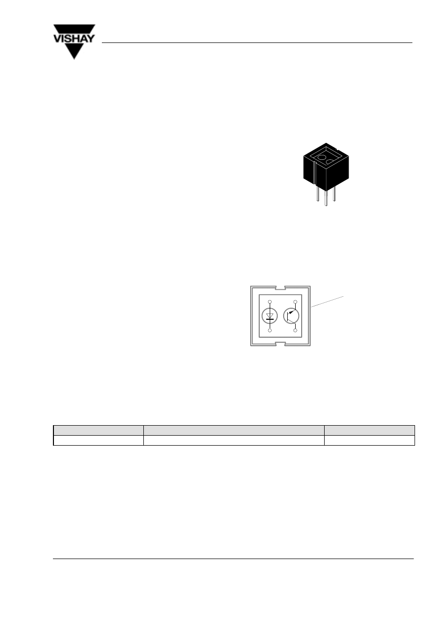
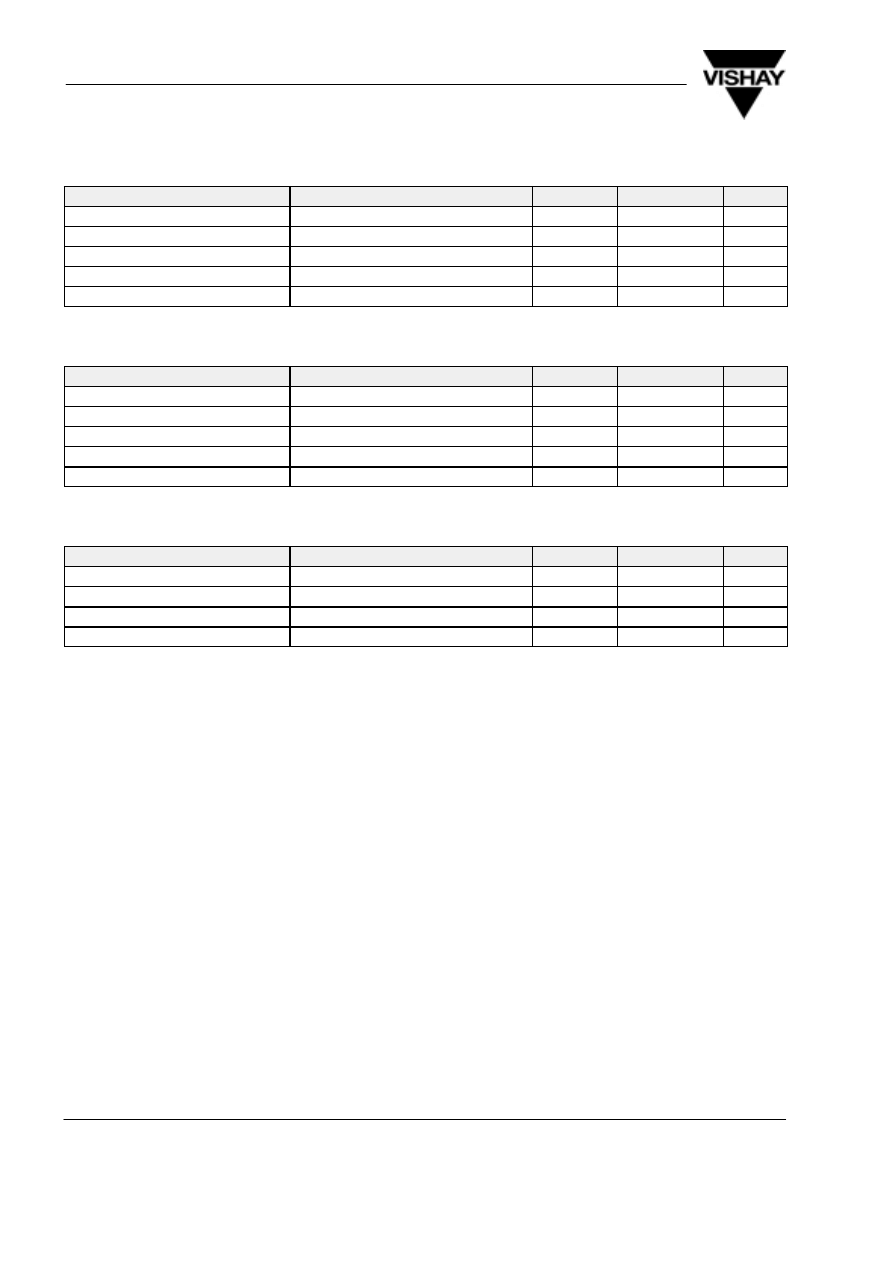
Reflective Optical Sensor with Transistor Output
Description
The CNY70 has a compact construction where the
emitting light source and the detector are arranged in
the same direction to sense the presence of an object
by using the reflective IR beam from the object.
The operating wavelength is 950 nm. The detector
consists of a phototransistor.
Applications
D
Optoelectronic scanning and switching devices
i.e., index sensing, coded disk scanning etc.
(optoelectronic encoder assemblies for
transmission sensing).
Features
D
Compact construction in center-to-center spacing
of 0.1’
D
No setting required
D
High signal output
D
Low temperature coefficient
D
Detector provided with optical filter
D
Current Transfer Ratio (CTR) of typical 5%
94 9320
95 10930
Marking aerea
D
E
Top view
Order Instruction
Ordering Code
Sensing Distance
Remarks
CNY70
0.3 mm
CNY70
Vishay Telefunken
www.vishay.
2 (7)
Rev. A4, 05–Jun–00
Document Number 83751
Absolute Maximum Ratings
Input (Emitter)
Parameter
Test Conditions
Symbol
Value
Unit
Reverse voltage
V
R
5
V
Forward current
I
F
50
mA
Forward surge current
t
p
≤
10
m
s
I
FSM
3
A
Power dissipation
T
amb
≤
25
°
C
P
V
100
mW
Junction temperature
T
j
100
°
C
Output (Detector)
Parameter
Test Conditions
Symbol
Value
Unit
Collector emitter voltage
V
CEO
32
V
Emitter collector voltage
V
ECO
7
V
Collector current
I
C
50
mA
Power dissipation
T
amb
≤
25
°
C
P
V
100
mW
Junction temperature
T
j
100
°
C
Coupler
Parameter
Test Conditions
Symbol
Value
Unit
Total power dissipation
T
amb
≤
25
°
C
P
tot
200
mW
Ambient temperature range
T
amb
–55 to +85
°
C
Storage temperature range
T
stg
–55 to +100
°
C
Soldering temperature
2 mm from case, t
≤
5 s
T
sd
260
°
C
CNY70
Vishay Telefunken
3 (7)
www.vishay.com
Document Number 83751
Rev. A4, 05–Apr–00
Electrical Characteristics
(T
amb
= 25
°
C)
Input (Emitter)
Parameter
Test Conditions
Symbol
Min.
Typ.
Max.
Unit
Forward voltage
I
F
= 50 mA
V
F
1.25
1.6
V
Output (Detector)
Parameter
Test Conditions
Symbol
Min.
Typ.
Max.
Unit
Collector emitter voltage
I
C
= 1 mA
V
CEO
32
V
Emitter collector voltage
I
E
= 100
m
A
V
ECO
5
V
Collector dark current
V
CE
= 20 V, I
f
= 0, E = 0
I
CEO
200
nA
Coupler
Parameter
Test Conditions
Symbol
Min.
Typ.
Max.
Unit
Collector current
V
CE
= 5 V, I
F
= 20 mA,
d = 0.3 mm (figure 1)
I
C
1)
0.3
1.0
mA
Cross talk current
V
CE
= 5 V, I
F
= 20 mA
(figure 1)
I
CX
2)
600
nA
Collector emitter satu-
ration voltage
I
F
= 20 mA, I
C
= 0.1 mA,
d = 0.3 mm (figure 1)
V
CEsat
1)
0.3
V
1)
Measured with the ‘Kodak neutral test card’, white side with 90% diffuse reflectance
2)
Measured without reflecting medium
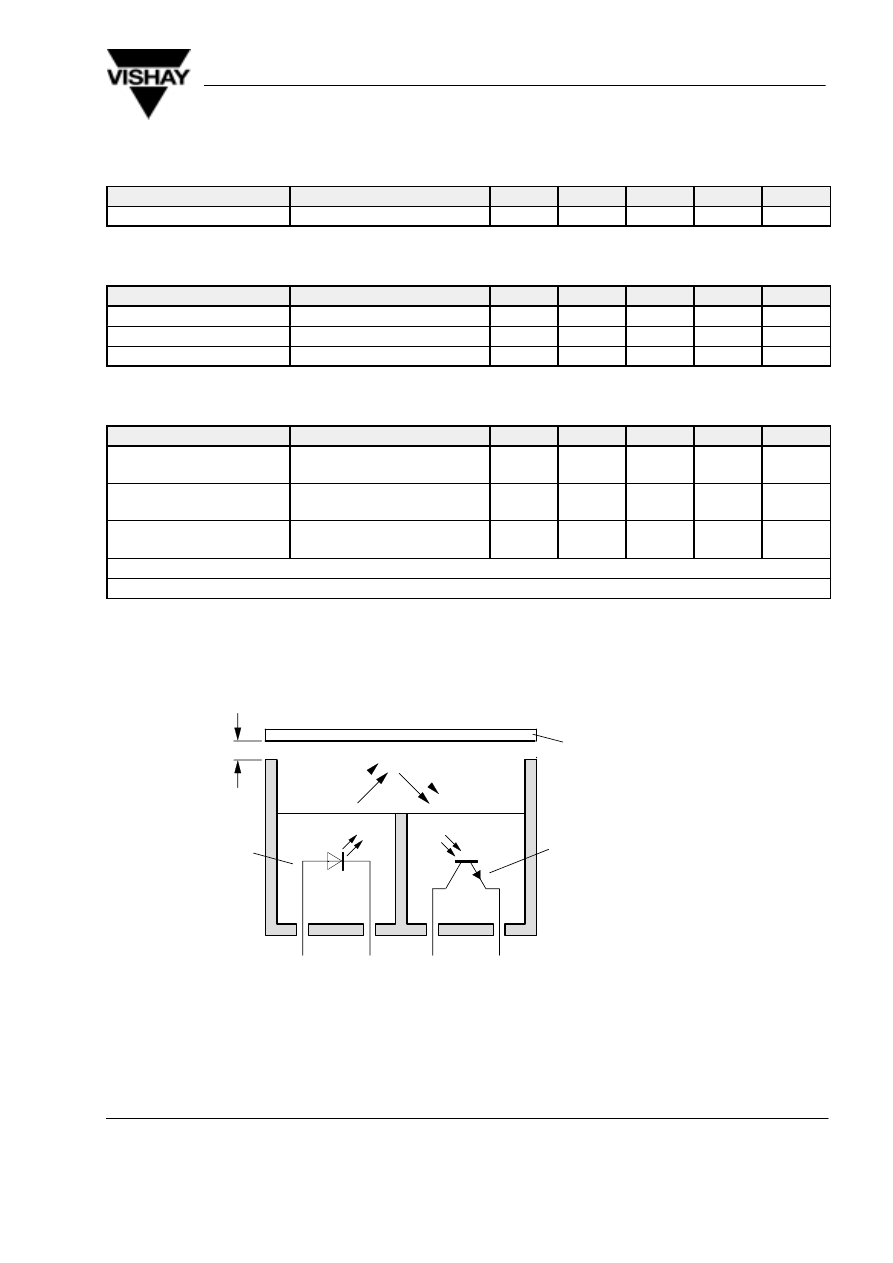
~~
~
~ ~
~
A
C
C
E
Detector
Emitter
d
Reflecting medium
(Kodak neutral test card)
95 10808
Figure 1. Test circuit
CNY70
Vishay Telefunken
www.vishay.
4 (7)
Rev. A4, 05–Jun–00
Document Number 83751
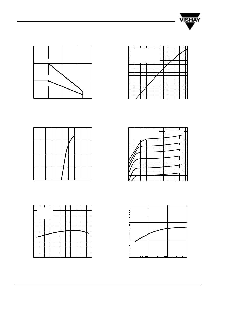
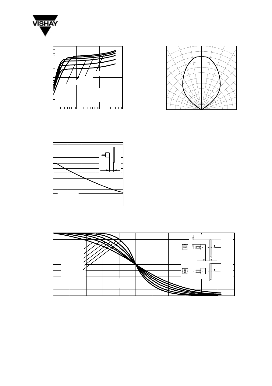
Typical Characteristics
(T
amb
= 25
_
C, unless otherwise specified)
0
100
200
300
0
25
50
75
100
95 11071
P
–
T
otal Power Dissipation ( mW
)
tot
T
amb
– Ambient Temperature (
°
C )
Coupled device
Phototransistor
IR-diode
Figure 2. Total Power Dissipation vs.
Ambient Temperature
0.1
1.0
10.0
100.0
1000.0
0
0.2 0.4 0.6 0.8 1.0 1.2 1.4 1.6 1.8 2.0
V
F
– Forward Voltage ( V )
96 11862
F
I – Forward Current ( mA
)
Figure 3. Forward Current vs. Forward Voltage
0.5
0.6
0.7
0.8
0.9
1.0
1.1
1.2
1.3
1.4
1.5
–30 –20 –10 0
10 20 30 40 50 60 70 80
T
amb
– Ambient Temperature (
°
C )
96 11913
CTR – Relative Current
T
ransfer
Ratio
rel
V
CE
=5V
I
F
=20mA
d=0.3
Figure 4. Relative Current Transfer Ratio vs.
Ambient Temperature
0.1
1
10
0.001
0.01
0.1
10
I – Collector Current ( mA
)
C
I
F
– Forward Current ( mA )
100
95 11065
1
Kodak Neutral Card
(White Side)
d=0.3
V
CE
=5V
Figure 5. Collector Current vs. Forward Current
0.1
1
10
0.01
0.1
1
10
V
CE
– Collector Emitter Voltage ( V )
100
95 11066
I – Collector Current ( mA
)
C
Kodak Neutral Card
(White Side)
d=0.3
I
F
= 50 mA
20 mA
10 mA
5 mA
2 mA
1 mA
Figure 6. Collector Current vs. Collector Emitter Voltage
0.1
1.0
10.0
100.0
0.1
1.0
10.0
100.0
I
F
– Forward Current ( mA )
96 11914
Kodak neutral card
(white side)
CTR – Current
T
ransfer Ratio ( % )
V
CE
=5V
d=0.3
Figure 7. Current Transfer Ratio vs. Forward Current
CNY70
Vishay Telefunken
5 (7)
www.vishay.com
Document Number 83751
Rev. A4, 05–Apr–00
0.1
1.0
10.0
0.1
1.0
10.0
100.0
V
CE
– Collector Emitter Voltage ( V )
96 12001
CTR
–
Current
T
ransfer Ratio ( % )
Kodak neutral card
(white side)
d=0.3
20mA
10mA
5mA
2mA
1mA
I
F
=50mA
Figure 8. Current Transfer Ratio vs.
Collector Emitter Voltage
0
2
4
6
8
0.001
0.1
1
10
I
–
Collector Current ( mA
)
C
d – Distance ( mm )
10
95 11069
V
CE
=5V
I
F
=20mA
d
Figure 9. Collector Current vs. Distance
0.4
0.2
0
0.2
0.4
I
–
Relative Radiant Intensity
e rel
0.6
95 11063
0.6
0.9
0.8
0
°
30
°
10
°
20
°
40
°
50
°
60
°
70
°
80
°
0.7
1.0
I
–
Relative Collector Current
c rel
Figure 10. Relative Radiant Intensity/Collector Current vs.
Displacement
0
0.1
0.2
0.3
0.4
0.5
0.6
0.7
0.8
0.9
1.0
0
1
2
3
4
5
6
7
8
9
10
11
s – Displacement ( mm )
96 11915
V
CE
= 5 V
I
F
= 20 mA
I
–
Relative Collector Current
Crel
d = 5 mm
4 mm
3 mm
2 mm
1 mm
0
E
D
D
E
1.5
d
s
0
5mm
10mm
s
0
5mm
10mm
Figure 11. Relative Collector Current vs. Displacement
CNY70
Vishay Telefunken
www.vishay.
6 (7)
Rev. A4, 05–Jun–00
Document Number 83751
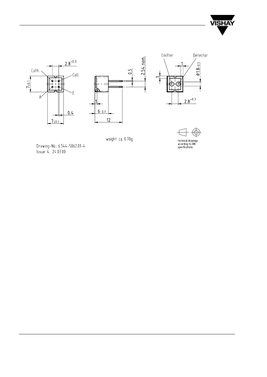
Dimensions of CNY70 in mm
95 11345

CNY70
Vishay Telefunken
7 (7)
www.vishay.com
Document Number 83751
Rev. A4, 05–Apr–00
Ozone Depleting Substances Policy Statement
It is the policy of Vishay Semiconductor GmbH to
1. Meet all present and future national and international statutory requirements.
2. Regularly and continuously improve the performance of our products, processes, distribution and operating
systems with respect to their impact on the health and safety of our employees and the public, as well as
their impact on the environment.
It is particular concern to control or eliminate releases of those substances into the atmosphere which are known as
ozone depleting substances ( ODSs ).
The Montreal Protocol ( 1987 ) and its London Amendments ( 1990 ) intend to severely restrict the use of ODSs and
forbid their use within the next ten years. Various national and international initiatives are pressing for an earlier ban
on these substances.
Vishay Semiconductor GmbH has been able to use its policy of continuous improvements to eliminate the use of
ODSs listed in the following documents.
1. Annex A, B and list of transitional substances of the Montreal Protocol and the London Amendments respectively
2 . Class I and II ozone depleting substances in the Clean Air Act Amendments of 1990 by the Environmental
Protection Agency ( EPA ) in the USA
3. Council Decision 88/540/EEC and 91/690/EEC Annex A, B and C ( transitional substances ) respectively.
Vishay Semiconductor GmbH can certify that our semiconductors are not manufactured with ozone depleting
substances and do not contain such substances.
We reserve the right to make changes to improve technical design and may do so without further notice.
Parameters can vary in different applications. All operating parameters must be validated for each customer application
by the customer. Should the buyer use Vishay Telefunken products for any unintended or unauthorized application, the
buyer shall indemnify Vishay Telefunken against all claims, costs, damages, and expenses, arising out of, directly or
indirectly, any claim of personal damage, injury or death associated with such unintended or unauthorized use.
Vishay Semiconductor GmbH, P.O.B. 3535, D-74025 Heilbronn, Germany
Telephone: 49 ( 0 ) 7131 67 2831, Fax number: 49 ( 0 ) 7131 67 2423
Wyszukiwarka
Podobne podstrony:
fetch datenblatt attiny26
fetch datenblatt 24c64
fetch datenblatt lm358
fetch datenblatt ntc02
Datenblatt KRC4
Datenblaetter im Web
EuroSprinter ES64 U4 2009 DE Datenblatt Laenderpakete CZ HR H PL SK SLO
fetch
EuroSprinter ES64 U4 2009 DE Datenblatt Laenderpakete A CH D I NL
Datenblatt iXSeries inventux DE
datenblatt jetnet3005 SCSL5NQEFRRAQNXGD5JIHJOVKGB526VCFKXEYHQ
HCM12T Datenblatt Web
Datenblatt STC Messung inventux EN
Datenblatt 118
Datenblatt AT90S2313
więcej podobnych podstron