
1
Embedded Systems Design: A Unified
Hardware/Software Introduction
Chapter 10: IC Technology

2
Embedded Systems Design: A Unified
Hardware/Software Introduction,
(c) 2000
Vahid/Givargis
Outline
• Anatomy of integrated circuits
• Full-Custom (VLSI) IC Technology
• Semi-Custom (ASIC) IC Technology
• Programmable Logic Device (PLD) IC
Technology
3
Embedded Systems Design: A Unified
Hardware/Software Introduction,
(c) 2000
Vahid/Givargis
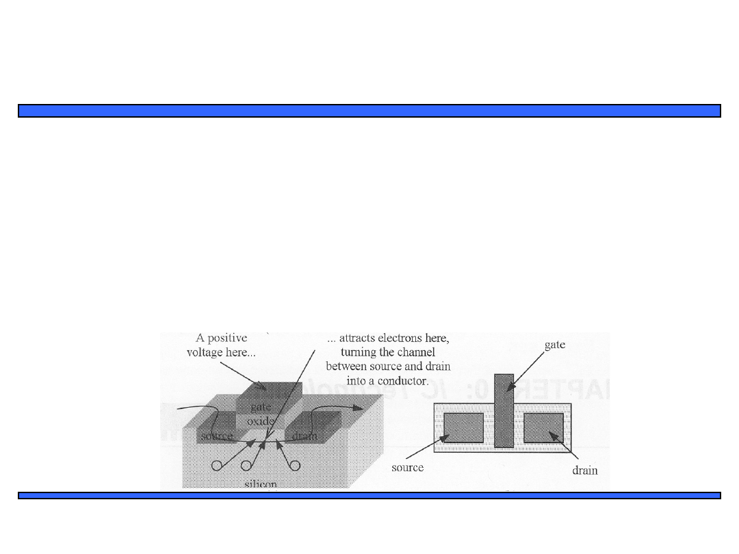
CMOS transistor
• Source, Drain
– Diffusion area where electrons can flow
– Can be connected to metal contacts (via’s)
• Gate
– Polysilicon area where control voltage is applied
• Oxide
– Si O
2
Insulator so the gate voltage can’t leak
4
Embedded Systems Design: A Unified
Hardware/Software Introduction,
(c) 2000
Vahid/Givargis
End of the Moore’s Law?
•
Every dimension of the MOSFET has to scale
– (PMOS) Gate oxide has to scale down to
• Increase gate capacitance
• Reduce leakage current from S to D
• Pinch off current from source to drain
– Current gate oxide thickness is about 2.5-3nm
•
That’s about 25 atoms!!!
source
drain
oxide
gate
IC
package
IC
chann
el
Silicon
substrate
5
Embedded Systems Design: A Unified
Hardware/Software Introduction,
(c) 2000
Vahid/Givargis
6
Embedded Systems Design: A Unified
Hardware/Software Introduction,
(c) 2000
Vahid/Givargis
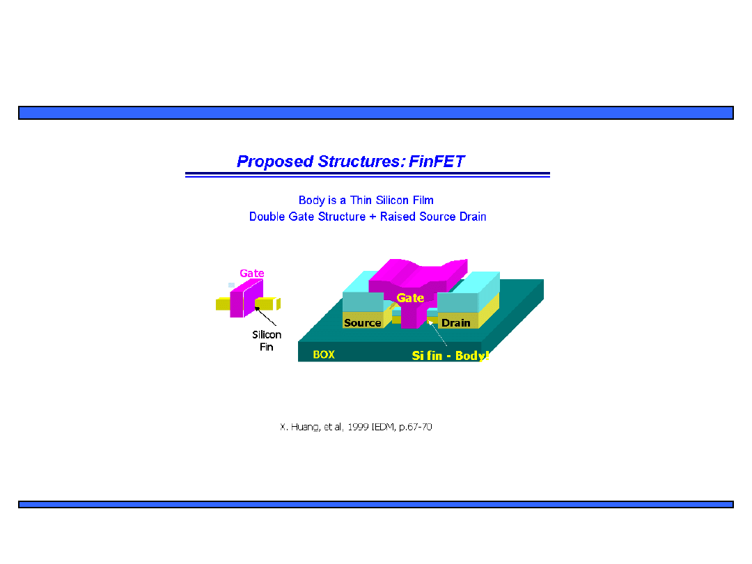
20Ghz +
• FinFET has been
manufactured to 18nm
– Still acts as a very good transistor
• Simulation shown that it can
be scaled to 10nm
– Quantum effect start to kick in
• Reduce mobility by ~10%
– Ballistic transport become
significant
• Increase current by about ~20%
7
Embedded Systems Design: A Unified
Hardware/Software Introduction,
(c) 2000
Vahid/Givargis
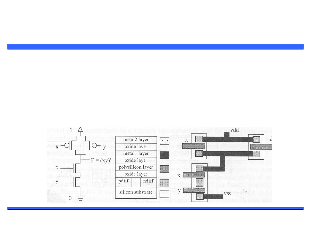
NAND
• Metal layers for routing (~10)
• PMOS don’t like 0
• NMOS don’t like 1
• A stick diagram form the basis for mask
sets
8
Embedded Systems Design: A Unified
Hardware/Software Introduction,
(c) 2000
Vahid/Givargis
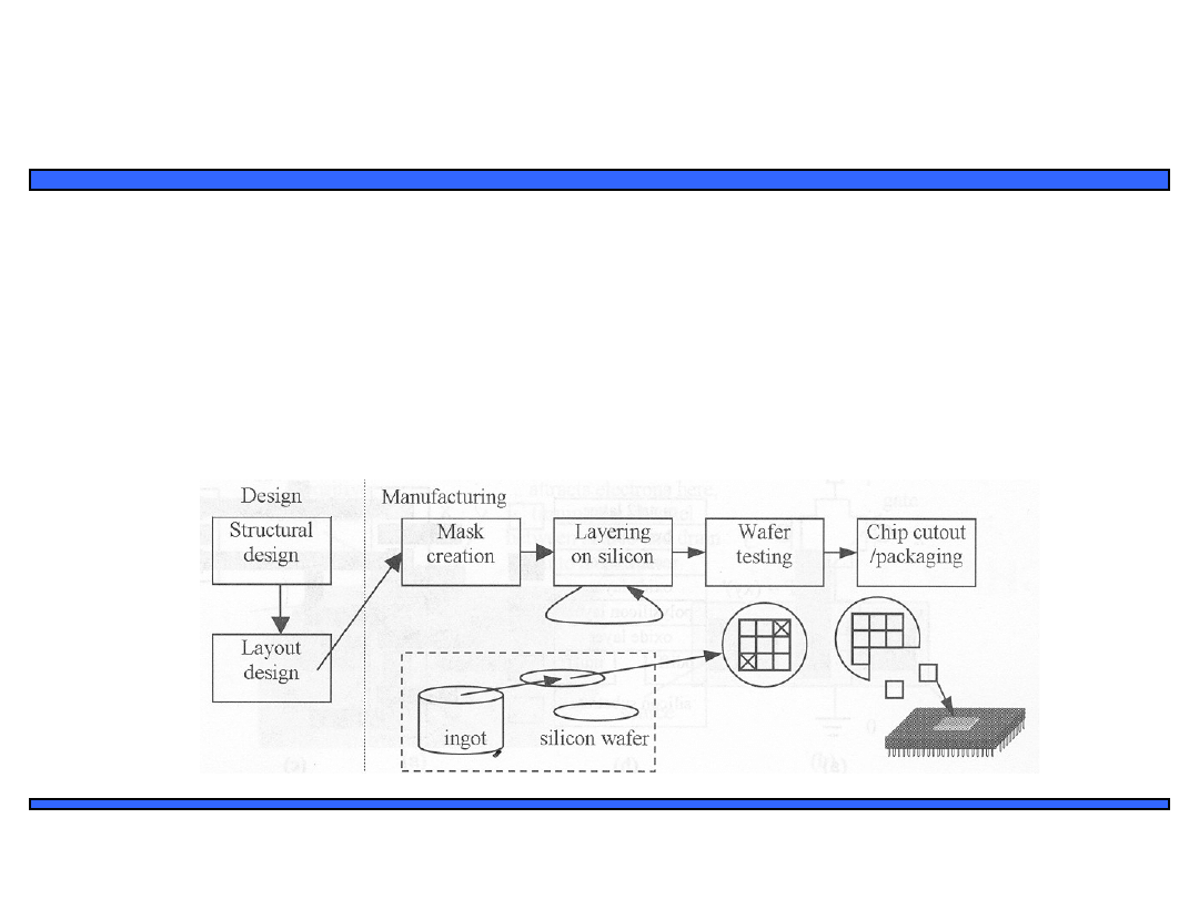
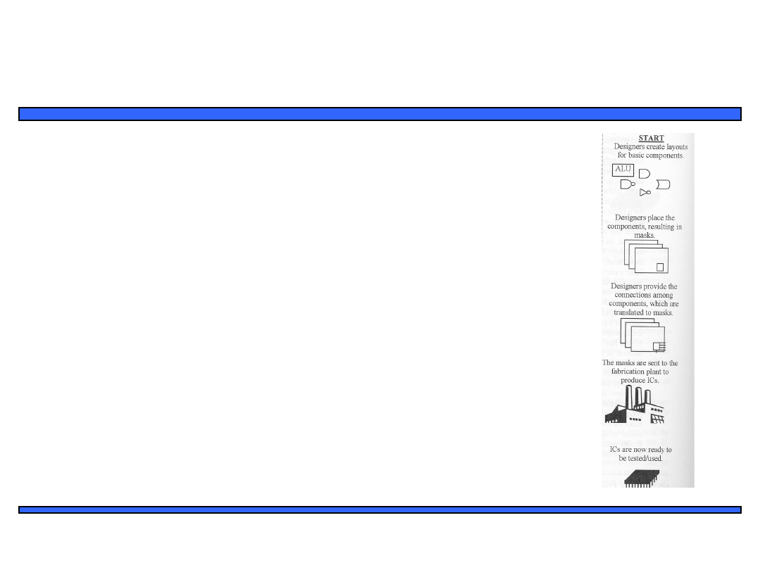
Silicon manufacturing steps
• Tape out
– Send design to manufacturing
• Spin
– One time through the manufacturing process
• Photolithography
– Drawing patterns by using photoresist to form barriers for deposition
9
Embedded Systems Design: A Unified
Hardware/Software Introduction,
(c) 2000
Vahid/Givargis
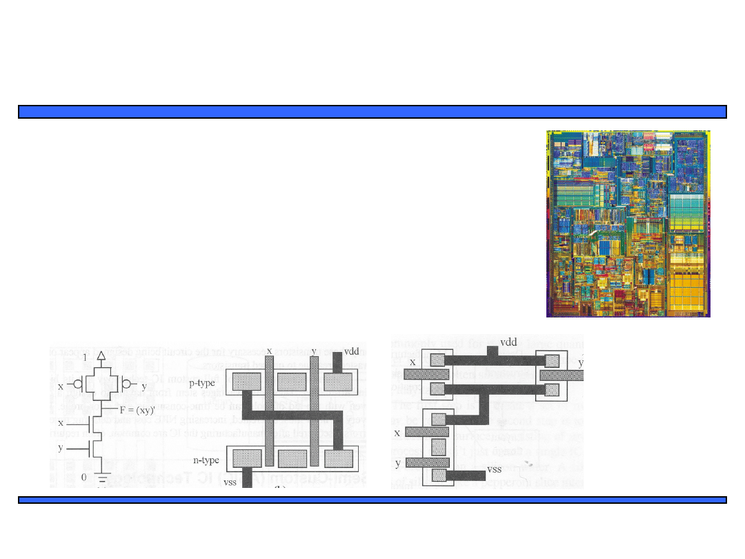
Full Custom
• Very Large Scale Integration (VLSI)
• Placement
– Place and orient transistors
• Routing
– Connect transistors
• Sizing
– Make fat, fast wires or thin, slow wires
– May also need to size buffer
• Design Rules
– “simple” rules for correct circuit function
• Metal/metal spacing, min poly width…
10
Embedded Systems Design: A Unified
Hardware/Software Introduction,
(c) 2000
Vahid/Givargis
Full Custom
• Best size, power, performance
• Hand design
– Horrible time-to-market/flexibility/NRE cost…
– Reserve for the most important units in a processor
• ALU, Instruction fetch…
• Physical design tools
– Less optimal, but faster…
11
Embedded Systems Design: A Unified
Hardware/Software Introduction,
(c) 2000
Vahid/Givargis
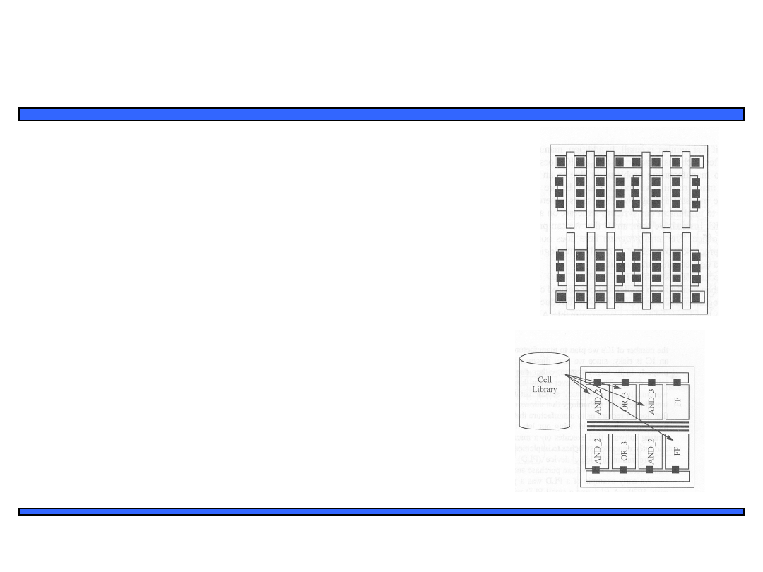
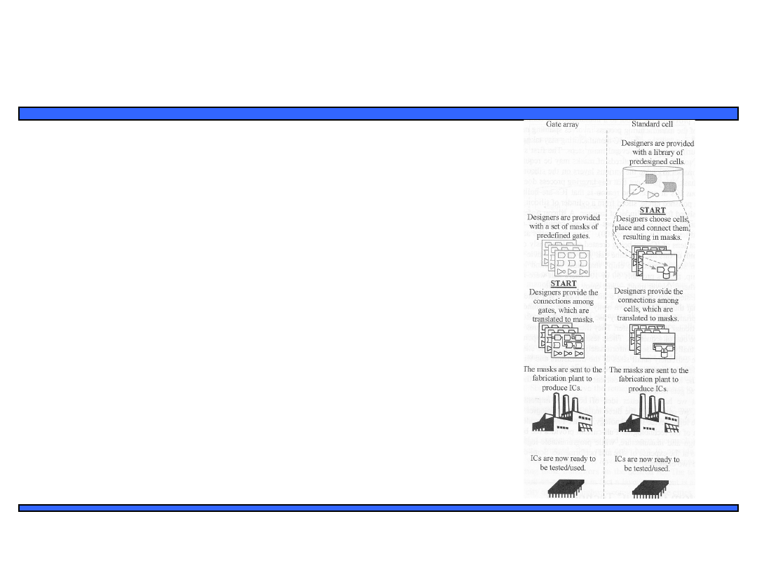
Semi-Custom
• Gate Array
– Array of prefabricated gates
– “place” and route
– Higher density, faster time-to-market
– Does not integrate as well with full-custom
• Standard Cell
– A library of pre-designed cell
– Place and route
– Lower density, higher complexity
– Integrate great with full-custom
12
Embedded Systems Design: A Unified
Hardware/Software Introduction,
(c) 2000
Vahid/Givargis
Semi-Custom
• Most popular design style
• Jack of all trade
– Good
• Power, time-to-market,
performance, NRE cost, per-
unit cost, area…
• Master of none
– Integrate with full custom
for critical regions of design
13
Embedded Systems Design: A Unified
Hardware/Software Introduction,
(c) 2000
Vahid/Givargis

14
Embedded Systems Design: A Unified
Hardware/Software Introduction,
(c) 2000
Vahid/Givargis
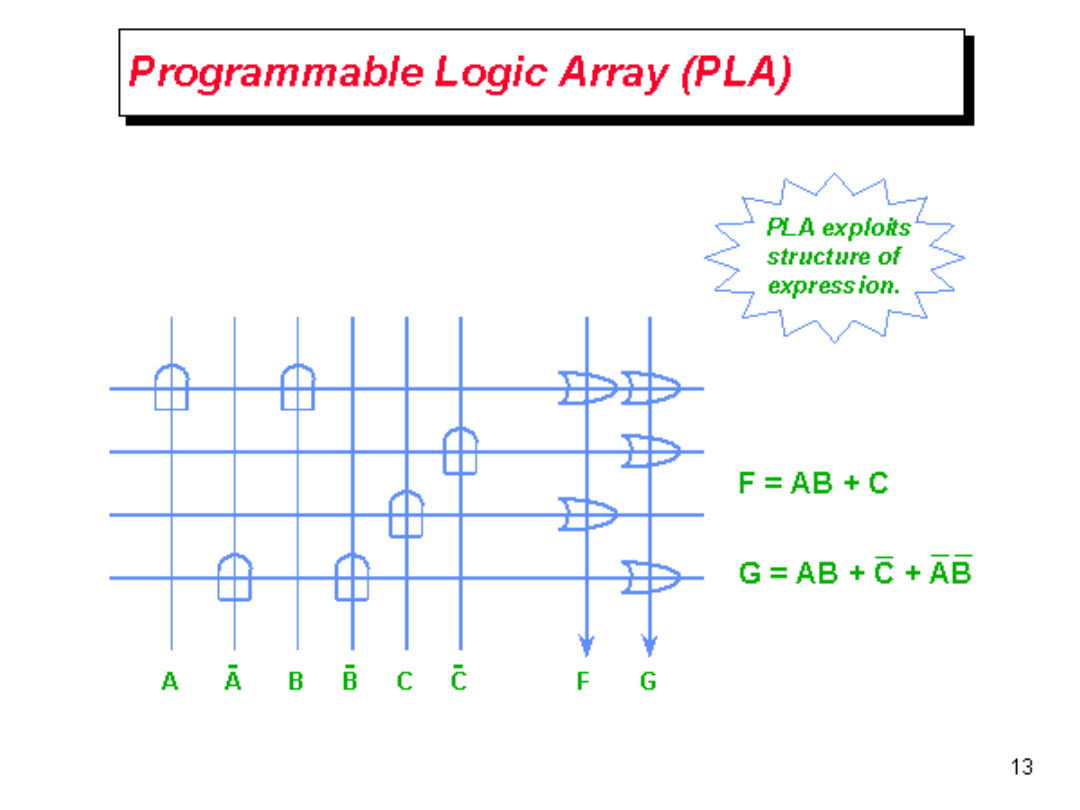
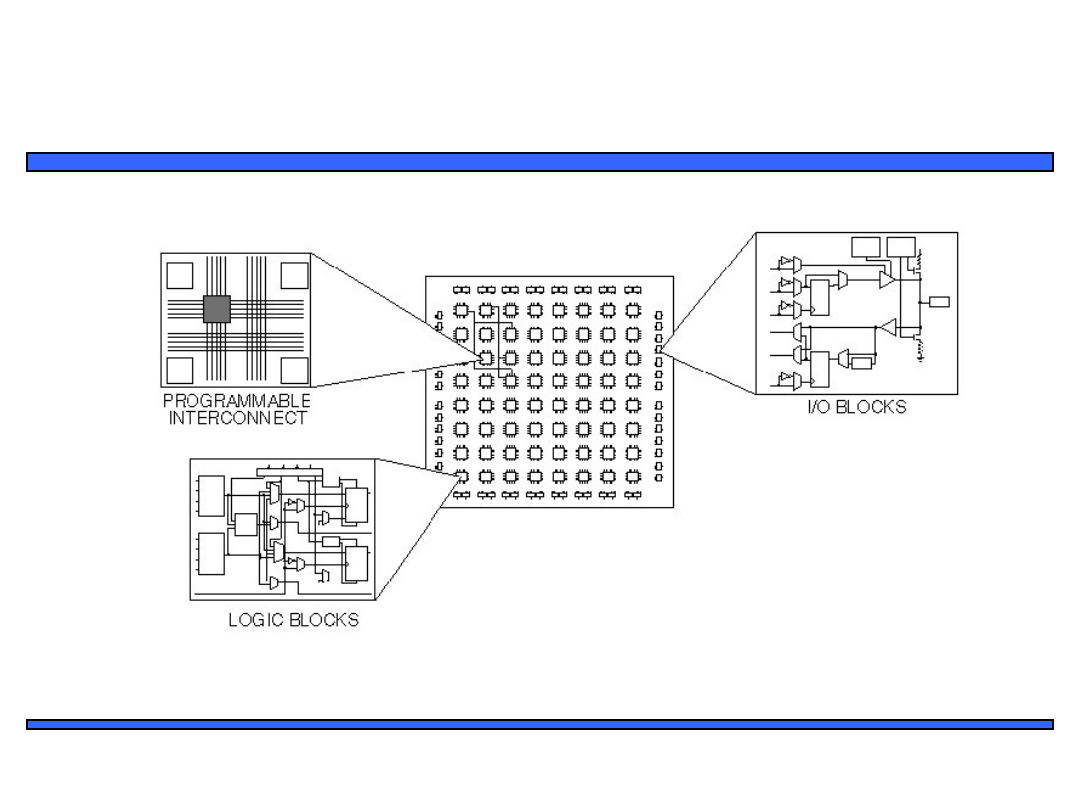
Programmable Logic Device
• Programmable Logic Device
– Programmable Logic Array, Programmable Array Logic, Field
Programmable Gate Array
• All layers already exist
– Designers can purchase an IC
– To implement desired functionality
• Connections on the IC are either created or destroyed to implement
• Benefits
– Very low NRE costs
– Great time to market
• Drawback
– High unit cost, bad for large volume
– Power
• Except special PLA
– slower
1600 usable gate, 7.5 ns
$7 list price
15
Embedded Systems Design: A Unified
Hardware/Software Introduction,
(c) 2000
Vahid/Givargis
Xilinx FPGA
16
Embedded Systems Design: A Unified
Hardware/Software Introduction,
(c) 2000
Vahid/Givargis
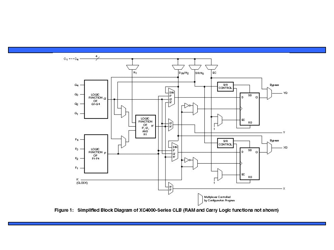
Configurable Logic Block (CLB)
17
Embedded Systems Design: A Unified
Hardware/Software Introduction,
(c) 2000
Vahid/Givargis
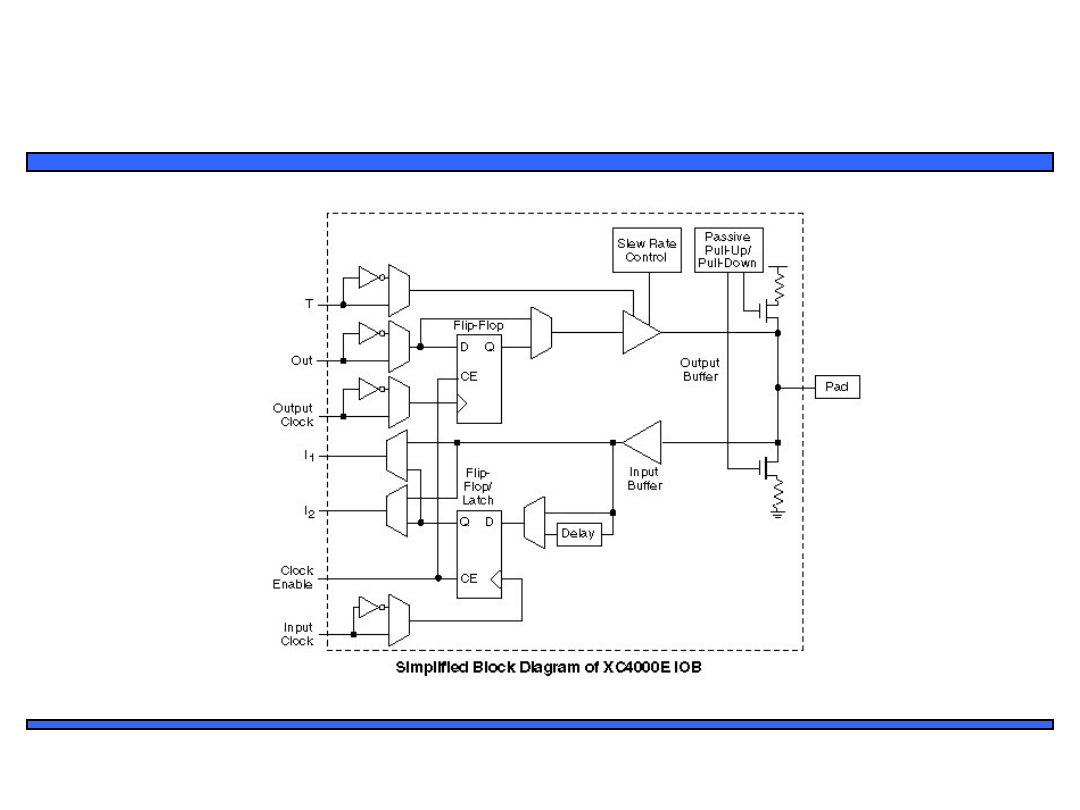
I/O Block
Document Outline
- Chapter 10: IC Technology
- Outline
- CMOS transistor
- End of the Moore’s Law?
- PowerPoint Presentation
- 20Ghz +
- NAND
- Silicon manufacturing steps
- Full Custom
- Slide 10
- Semi-Custom
- Semi-Custom
- Slide 13
- Programmable Logic Device
- Xilinx FPGA
- Configurable Logic Block (CLB)
- I/O Block
Wyszukiwarka
Podobne podstrony:
Ch10 Q3
ch10
Ch10 E2
Ch10 Q1
BW ch10
Ch10 Q5
ch10
ch10
ch10
Ch10 Placed Features
Ch10 Standard Parts
Ch10 E3
ch10, Sieci Komputerowe Cisco
ch9 012604
Ch10 NuclearPowerPlant
cisco2 ch10 focus SL24PPCZXC45HY33A2JRSIZJD3UAHAWWEJ7R7RY
CH10
Ch10
Ch10 Q4
więcej podobnych podstron