Complementary Silicon
High-Power Transistors
. . . PowerBase
complementary transistors designed for high
power audio, stepping motor and other linear applications. These
devices can also be used in power switching circuits such as relay or
solenoid drivers, dc–to–dc converters, inverters, or for inductive loads
requiring higher safe operating area than the 2N3055 and MJ2955.
•
Current–Gain — Bandwidth–Product @ I
C
= 1.0 Adc
f
T
= 0.8 MHz (Min) – NPN
= 2.2 MHz (Min) – PNP
•
Safe Operating Area — Rated to 60 V and 120 V, Respectively
ÎÎÎÎÎÎÎÎÎÎÎÎÎÎÎÎÎÎÎÎÎÎÎ
ÎÎÎÎÎÎÎÎÎÎÎÎÎÎÎÎÎÎÎÎÎÎÎ
*MAXIMUM RATINGS
ÎÎÎÎÎÎÎÎÎÎÎ
Î
ÎÎÎÎÎÎÎÎÎ
Î
ÎÎÎÎÎÎÎÎÎÎÎ
Rating
ÎÎÎÎÎ
Î
ÎÎÎ
Î
ÎÎÎÎÎ
Symbol
ÎÎÎÎ
Î
ÎÎ
Î
ÎÎÎÎ
2N3055A
MJ2955A
ÎÎÎÎ
Î
ÎÎ
Î
ÎÎÎÎ
MJ15015
MJ15016
ÎÎÎ
Î
Î
Î
ÎÎÎ
Unit
ÎÎÎÎÎÎÎÎÎÎÎ
ÎÎÎÎÎÎÎÎÎÎÎ
Collector–Emitter Voltage
ÎÎÎÎÎ
ÎÎÎÎÎ
V
CEO
ÎÎÎÎ
ÎÎÎÎ
60
ÎÎÎÎ
ÎÎÎÎ
120
ÎÎÎ
ÎÎÎ
Vdc
ÎÎÎÎÎÎÎÎÎÎÎ
ÎÎÎÎÎÎÎÎÎÎÎ
Collector–Base Voltage
ÎÎÎÎÎ
ÎÎÎÎÎ
V
CBO
ÎÎÎÎ
ÎÎÎÎ
100
ÎÎÎÎ
ÎÎÎÎ
200
ÎÎÎ
ÎÎÎ
Vdc
ÎÎÎÎÎÎÎÎÎÎÎ
Î
ÎÎÎÎÎÎÎÎÎ
Î
ÎÎÎÎÎÎÎÎÎÎÎ
Collector–Emitter Voltage Base
Reversed Biased
ÎÎÎÎÎ
Î
ÎÎÎ
Î
ÎÎÎÎÎ
V
CEV
ÎÎÎÎ
Î
ÎÎ
Î
ÎÎÎÎ
100
ÎÎÎÎ
Î
ÎÎ
Î
ÎÎÎÎ
200
ÎÎÎ
Î
Î
Î
ÎÎÎ
Vdc
ÎÎÎÎÎÎÎÎÎÎÎ
ÎÎÎÎÎÎÎÎÎÎÎ
Emitter–Base Voltage
ÎÎÎÎÎ
ÎÎÎÎÎ
V
EBO
ÎÎÎÎÎÎÎ
ÎÎÎÎÎÎÎ
7.0
ÎÎÎ
ÎÎÎ
Vdc
ÎÎÎÎÎÎÎÎÎÎÎ
ÎÎÎÎÎÎÎÎÎÎÎ
Collector Current — Continuous
ÎÎÎÎÎ
ÎÎÎÎÎ
I
C
ÎÎÎÎÎÎÎ
ÎÎÎÎÎÎÎ
15
ÎÎÎ
ÎÎÎ
Adc
ÎÎÎÎÎÎÎÎÎÎÎ
ÎÎÎÎÎÎÎÎÎÎÎ
Base Current
ÎÎÎÎÎ
ÎÎÎÎÎ
I
B
ÎÎÎÎÎÎÎ
ÎÎÎÎÎÎÎ
7.0
ÎÎÎ
ÎÎÎ
Adc
ÎÎÎÎÎÎÎÎÎÎÎ
Î
ÎÎÎÎÎÎÎÎÎ
Î
ÎÎÎÎÎÎÎÎÎÎÎ
Total Device Dissipation @ T
C
= 25
C
Derate above 25
C
ÎÎÎÎÎ
Î
ÎÎÎ
Î
ÎÎÎÎÎ
P
D
ÎÎÎÎ
Î
ÎÎ
Î
ÎÎÎÎ
115
0.65
ÎÎÎÎ
Î
ÎÎ
Î
ÎÎÎÎ
180
1.03
ÎÎÎ
Î
Î
Î
ÎÎÎ
Watts
W/
C
ÎÎÎÎÎÎÎÎÎÎÎ
Î
ÎÎÎÎÎÎÎÎÎ
Î
ÎÎÎÎÎÎÎÎÎÎÎ
Operating and Storage Junction
Temperature Range
ÎÎÎÎÎ
Î
ÎÎÎ
Î
ÎÎÎÎÎ
T
J
, T
stg
ÎÎÎÎÎÎÎ
Î
ÎÎÎÎÎ
Î
ÎÎÎÎÎÎÎ
–65 to +200
ÎÎÎ
Î
Î
Î
ÎÎÎ
C
ÎÎÎÎÎÎÎÎÎÎÎÎÎÎÎÎÎÎÎÎÎÎÎ
ÎÎÎÎÎÎÎÎÎÎÎÎÎÎÎÎÎÎÎÎÎÎÎ
THERMAL CHARACTERISTICS
ÎÎÎÎÎÎÎÎÎÎÎ
ÎÎÎÎÎÎÎÎÎÎÎ
Characteristic
ÎÎÎÎÎ
ÎÎÎÎÎ
Symbol
ÎÎÎÎ
ÎÎÎÎ
Max
ÎÎÎÎ
ÎÎÎÎ
Max
ÎÎÎ
ÎÎÎ
Unit
ÎÎÎÎÎÎÎÎÎÎÎ
Î
ÎÎÎÎÎÎÎÎÎ
Î
ÎÎÎÎÎÎÎÎÎÎÎ
Thermal Resistance, Junction to Case
ÎÎÎÎÎ
Î
ÎÎÎ
Î
ÎÎÎÎÎ
R
θ
JC
ÎÎÎÎ
Î
ÎÎ
Î
ÎÎÎÎ
1.52
ÎÎÎÎ
Î
ÎÎ
Î
ÎÎÎÎ
0.98
ÎÎÎ
Î
Î
Î
ÎÎÎ
C/W
*Indicates JEDEC Registered Data. (2N3055A)
Preferred devices are ON Semiconductor recommended choices for future use and best overall value.
ON Semiconductor
Semiconductor Components Industries, LLC, 2001
March, 2001 – Rev. 3
1
Publication Order Number:
2N3055A/D
2N3055A
MJ15015
MJ2955A
MJ15016
*ON Semiconductor Preferred Device
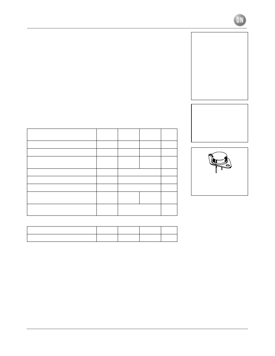
15 AMPERE
COMPLEMENTARY
SILICON
POWER TRANSISTORS
60, 120 VOLTS
115, 180 WATTS
CASE 1–07
TO–204AA
(TO–3)
*
*
NPN
PNP
2N3055A MJ15015 MJ2955A MJ15016
http://onsemi.com
2
200
0
0
25
50
75
100
125
150
175
200
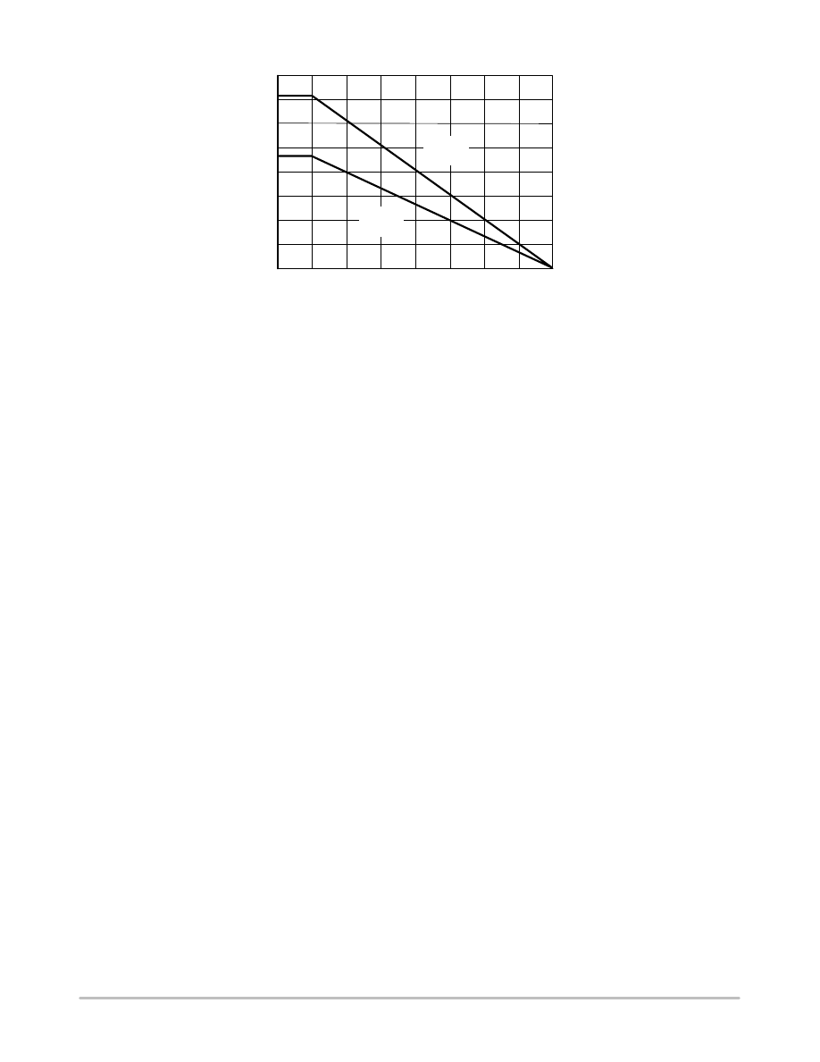
Figure 1. Power Derating
T
C
, CASE TEMPERATURE (
°
C)
MJ15015
MJ15016
P ,
AVERAGE POWER DISSIP
ATION (W)
D(A
V)
150
100
50
2N3055A
MJ2955A
2N3055A MJ15015 MJ2955A MJ15016
http://onsemi.com
3
ÎÎÎÎÎÎÎÎÎÎÎÎÎÎÎÎÎÎÎÎÎÎÎÎÎÎÎÎÎÎÎÎÎÎ
ÎÎÎÎÎÎÎÎÎÎÎÎÎÎÎÎÎÎÎÎÎÎÎÎÎÎÎÎÎÎÎÎÎÎ
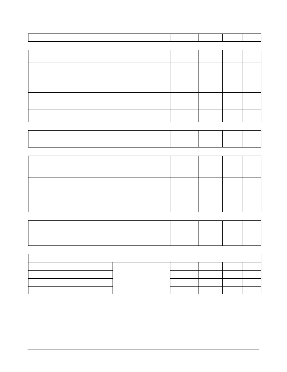
ELECTRICAL CHARACTERISTICS
(T
C
= 25
°
C unless otherwise noted)
ÎÎÎÎÎÎÎÎÎÎÎÎÎÎÎÎÎÎÎÎÎ
ÎÎÎÎÎÎÎÎÎÎÎÎÎÎÎÎÎÎÎÎÎ
Characteristic
ÎÎÎÎÎ
ÎÎÎÎÎ
Symbol
ÎÎÎÎ
ÎÎÎÎ
Min
ÎÎÎÎ
ÎÎÎÎ
Max
ÎÎÎÎ
ÎÎÎÎ
Unit
ÎÎÎÎÎÎÎÎÎÎÎÎÎÎÎÎÎÎÎÎÎÎÎÎÎÎÎÎÎÎÎÎÎÎ
ÎÎÎÎÎÎÎÎÎÎÎÎÎÎÎÎÎÎÎÎÎÎÎÎÎÎÎÎÎÎÎÎÎÎ
OFF CHARACTERISTICS (1)
ÎÎÎÎÎÎÎÎÎÎÎÎÎÎÎÎÎÎÎÎÎ
Î
ÎÎÎÎÎÎÎÎÎÎÎÎÎÎÎÎÎÎÎ
Î
ÎÎÎÎÎÎÎÎÎÎÎÎÎÎÎÎÎÎÎÎÎ
*Collector–Emitter Sustaining Voltage
2N3055A, MJ2955A
(I
C
= 200 mAdc, I
B
= 0)
MJ15015, MJ15016
ÎÎÎÎÎ
Î
ÎÎÎ
Î
ÎÎÎÎÎ
V
CEO(sus)
ÎÎÎÎ
Î
ÎÎ
Î
ÎÎÎÎ
60
120
ÎÎÎÎ
Î
ÎÎ
Î
ÎÎÎÎ
—
—
ÎÎÎÎ
Î
ÎÎ
Î
ÎÎÎÎ
Vdc
ÎÎÎÎÎÎÎÎÎÎÎÎÎÎÎÎÎÎÎÎÎ
Î
ÎÎÎÎÎÎÎÎÎÎÎÎÎÎÎÎÎÎÎ
Î
Î
ÎÎÎÎÎÎÎÎÎÎÎÎÎÎÎÎÎÎÎ
Î
ÎÎÎÎÎÎÎÎÎÎÎÎÎÎÎÎÎÎÎÎÎ
Collector Cutoff Current
(V
CE
= 30 Vdc, V
BE(off)
= 0 Vdc)
2N3055A, MJ2955A
(V
CE
= 60 Vdc, V
BE(off)
= 0 Vdc)
MJ15015, MJ15016
ÎÎÎÎÎ
Î
ÎÎÎ
Î
Î
ÎÎÎ
Î
ÎÎÎÎÎ
I
CEO
ÎÎÎÎ
Î
ÎÎ
Î
Î
ÎÎ
Î
ÎÎÎÎ
—
—
ÎÎÎÎ
Î
ÎÎ
Î
Î
ÎÎ
Î
ÎÎÎÎ
0.7
0.1
ÎÎÎÎ
Î
ÎÎ
Î
Î
ÎÎ
Î
ÎÎÎÎ
mAdc
ÎÎÎÎÎÎÎÎÎÎÎÎÎÎÎÎÎÎÎÎÎ
ÎÎÎÎÎÎÎÎÎÎÎÎÎÎÎÎÎÎÎÎÎ
*Collector Cutoff Current
2N3055A, MJ2955A
(V
CEV
= Rated Value, V
BE(off)
= 1.5 Vdc)
MJ15015, MJ15016
ÎÎÎÎÎ
ÎÎÎÎÎ
I
CEV
ÎÎÎÎ
ÎÎÎÎ
—
—
ÎÎÎÎ
ÎÎÎÎ
5.0
1.0
ÎÎÎÎ
ÎÎÎÎ
mAdc
ÎÎÎÎÎÎÎÎÎÎÎÎÎÎÎÎÎÎÎÎÎ
Î
ÎÎÎÎÎÎÎÎÎÎÎÎÎÎÎÎÎÎÎ
Î
Î
ÎÎÎÎÎÎÎÎÎÎÎÎÎÎÎÎÎÎÎ
Î
ÎÎÎÎÎÎÎÎÎÎÎÎÎÎÎÎÎÎÎÎÎ
Collector Cutoff Current
(V
CEV
= Rated Value, V
BE(off)
= 1.5 Vdc,
2N3055A, MJ2955A
T
C
= 150
C)
MJ15015, MJ15016
ÎÎÎÎÎ
Î
ÎÎÎ
Î
Î
ÎÎÎ
Î
ÎÎÎÎÎ
I
CEV
ÎÎÎÎ
Î
ÎÎ
Î
Î
ÎÎ
Î
ÎÎÎÎ
—
—
ÎÎÎÎ
Î
ÎÎ
Î
Î
ÎÎ
Î
ÎÎÎÎ
30
6.0
ÎÎÎÎ
Î
ÎÎ
Î
Î
ÎÎ
Î
ÎÎÎÎ
mAdc
ÎÎÎÎÎÎÎÎÎÎÎÎÎÎÎÎÎÎÎÎÎ
ÎÎÎÎÎÎÎÎÎÎÎÎÎÎÎÎÎÎÎÎÎ
Emitter Cutoff Current
2N3055A, MJ2955A
(V
EB
= 7.0 Vdc, I
C
= 0)
MJ15015, MJ15016
ÎÎÎÎÎ
ÎÎÎÎÎ
I
EBO
ÎÎÎÎ
ÎÎÎÎ
—
—
ÎÎÎÎ
ÎÎÎÎ
5.0
0.2
ÎÎÎÎ
ÎÎÎÎ
mAdc
ÎÎÎÎÎÎÎÎÎÎÎÎÎÎÎÎÎÎÎÎÎÎÎÎÎÎÎÎÎÎÎÎÎÎ
Î
ÎÎÎÎÎÎÎÎÎÎÎÎÎÎÎÎÎÎÎÎÎÎÎÎÎÎÎÎÎÎÎÎ
Î
ÎÎÎÎÎÎÎÎÎÎÎÎÎÎÎÎÎÎÎÎÎÎÎÎÎÎÎÎÎÎÎÎÎÎ
*SECOND BREAKDOWN
ÎÎÎÎÎÎÎÎÎÎÎÎÎÎÎÎÎÎÎÎÎ
Î
ÎÎÎÎÎÎÎÎÎÎÎÎÎÎÎÎÎÎÎ
Î
ÎÎÎÎÎÎÎÎÎÎÎÎÎÎÎÎÎÎÎÎÎ
Second Breakdown Collector Current with Base Forward Biased
(t = 0.5 s non–repetitive)
2N3055A, MJ2955A
(V
CE
= 60 Vdc)
MJ15015, MJ15016
ÎÎÎÎÎ
Î
ÎÎÎ
Î
ÎÎÎÎÎ
I
S/b
ÎÎÎÎ
Î
ÎÎ
Î
ÎÎÎÎ
1.95
3.0
ÎÎÎÎ
Î
ÎÎ
Î
ÎÎÎÎ
—
—
ÎÎÎÎ
Î
ÎÎ
Î
ÎÎÎÎ
Adc
ÎÎÎÎÎÎÎÎÎÎÎÎÎÎÎÎÎÎÎÎÎÎÎÎÎÎÎÎÎÎÎÎÎÎ
ÎÎÎÎÎÎÎÎÎÎÎÎÎÎÎÎÎÎÎÎÎÎÎÎÎÎÎÎÎÎÎÎÎÎ
*ON CHARACTERISTICS (1)
ÎÎÎÎÎÎÎÎÎÎÎÎÎÎÎÎÎÎÎÎÎ
Î
ÎÎÎÎÎÎÎÎÎÎÎÎÎÎÎÎÎÎÎ
Î
Î
ÎÎÎÎÎÎÎÎÎÎÎÎÎÎÎÎÎÎÎ
Î
ÎÎÎÎÎÎÎÎÎÎÎÎÎÎÎÎÎÎÎÎÎ
DC Current Gain
(I
C
= 4.0 Adc, V
CE
= 2.0 Vdc)
(I
C
= 4.0 Adc, V
CE
= 4.0 Vdc)
(I
C
= 10 Adc, V
CE
= 4.0 Vdc)
ÎÎÎÎÎ
Î
ÎÎÎ
Î
Î
ÎÎÎ
Î
ÎÎÎÎÎ
h
FE
ÎÎÎÎ
Î
ÎÎ
Î
Î
ÎÎ
Î
ÎÎÎÎ
10
20
5.0
ÎÎÎÎ
Î
ÎÎ
Î
Î
ÎÎ
Î
ÎÎÎÎ
70
70
—
ÎÎÎÎ
Î
ÎÎ
Î
Î
ÎÎ
Î
ÎÎÎÎ
—
ÎÎÎÎÎÎÎÎÎÎÎÎÎÎÎÎÎÎÎÎÎ
Î
ÎÎÎÎÎÎÎÎÎÎÎÎÎÎÎÎÎÎÎ
Î
Î
ÎÎÎÎÎÎÎÎÎÎÎÎÎÎÎÎÎÎÎ
Î
ÎÎÎÎÎÎÎÎÎÎÎÎÎÎÎÎÎÎÎÎÎ
Collector–Emitter Saturation Voltage
(I
C
= 4.0 Adc, I
B
= 400 mAdc)
(I
C
= 10 Adc, I
B
= 3.3 Adc)
(I
C
= 15 Adc, I
B
= 7.0 Adc)
ÎÎÎÎÎ
Î
ÎÎÎ
Î
Î
ÎÎÎ
Î
ÎÎÎÎÎ
V
CE(sat)
ÎÎÎÎ
Î
ÎÎ
Î
Î
ÎÎ
Î
ÎÎÎÎ
—
—
—
ÎÎÎÎ
Î
ÎÎ
Î
Î
ÎÎ
Î
ÎÎÎÎ
1.1
3.0
5.0
ÎÎÎÎ
Î
ÎÎ
Î
Î
ÎÎ
Î
ÎÎÎÎ
Vdc
ÎÎÎÎÎÎÎÎÎÎÎÎÎÎÎÎÎÎÎÎÎ
Î
ÎÎÎÎÎÎÎÎÎÎÎÎÎÎÎÎÎÎÎ
Î
ÎÎÎÎÎÎÎÎÎÎÎÎÎÎÎÎÎÎÎÎÎ
Base–Emitter On Voltage
(I
C
= 4.0 Adc, V
CE
= 4.0 Vdc)
ÎÎÎÎÎ
Î
ÎÎÎ
Î
ÎÎÎÎÎ
V
BE(on)
ÎÎÎÎ
Î
ÎÎ
Î
ÎÎÎÎ
0.7
ÎÎÎÎ
Î
ÎÎ
Î
ÎÎÎÎ
1.8
ÎÎÎÎ
Î
ÎÎ
Î
ÎÎÎÎ
Vdc
ÎÎÎÎÎÎÎÎÎÎÎÎÎÎÎÎÎÎÎÎÎÎÎÎÎÎÎÎÎÎÎÎÎÎ
ÎÎÎÎÎÎÎÎÎÎÎÎÎÎÎÎÎÎÎÎÎÎÎÎÎÎÎÎÎÎÎÎÎÎ
*DYNAMIC CHARACTERISTICS
ÎÎÎÎÎÎÎÎÎÎÎÎÎÎÎÎÎÎÎÎÎ
Î
ÎÎÎÎÎÎÎÎÎÎÎÎÎÎÎÎÎÎÎ
Î
ÎÎÎÎÎÎÎÎÎÎÎÎÎÎÎÎÎÎÎÎÎ
Current–Gain — Bandwidth Product
2N3055A, MJ15015
(I
C
= 1.0 Adc, V
CE
= 4.0 Vdc, f = 1.0 MHz)
MJ2955A, MJ15016
ÎÎÎÎÎ
Î
ÎÎÎ
Î
ÎÎÎÎÎ
f
T
ÎÎÎÎ
Î
ÎÎ
Î
ÎÎÎÎ
0.8
2.2
ÎÎÎÎ
Î
ÎÎ
Î
ÎÎÎÎ
6.0
18
ÎÎÎÎ
Î
ÎÎ
Î
ÎÎÎÎ
MHz
ÎÎÎÎÎÎÎÎÎÎÎÎÎÎÎÎÎÎÎÎÎ
Î
ÎÎÎÎÎÎÎÎÎÎÎÎÎÎÎÎÎÎÎ
Î
ÎÎÎÎÎÎÎÎÎÎÎÎÎÎÎÎÎÎÎÎÎ
Output Capacitance
(V
CB
= 10 Vdc, I
E
= 0, f = 1.0 MHz)
ÎÎÎÎÎ
Î
ÎÎÎ
Î
ÎÎÎÎÎ
C
ob
ÎÎÎÎ
Î
ÎÎ
Î
ÎÎÎÎ
60
ÎÎÎÎ
Î
ÎÎ
Î
ÎÎÎÎ
600
ÎÎÎÎ
Î
ÎÎ
Î
ÎÎÎÎ
pF
ÎÎÎÎÎÎÎÎÎÎÎÎÎÎÎÎÎÎÎÎÎÎÎÎÎÎÎÎÎÎÎÎÎÎ
ÎÎÎÎÎÎÎÎÎÎÎÎÎÎÎÎÎÎÎÎÎÎÎÎÎÎÎÎÎÎÎÎÎÎ
*SWITCHING CHARACTERISTICS (2N3055A only)
ÎÎÎÎÎÎÎÎÎÎÎÎÎÎÎÎÎÎÎÎÎÎÎÎÎÎÎÎÎÎÎÎÎÎ
ÎÎÎÎÎÎÎÎÎÎÎÎÎÎÎÎÎÎÎÎÎÎÎÎÎÎÎÎÎÎÎÎÎÎ
RESISTIVE LOAD
ÎÎÎÎÎÎÎÎÎÎÎÎÎ
ÎÎÎÎÎÎÎÎÎÎÎÎÎ
Delay Time
ÎÎÎÎÎÎÎÎÎ
ÎÎÎÎÎÎÎÎÎ
ÎÎÎÎÎ
ÎÎÎÎÎ
t
d
ÎÎÎÎ
ÎÎÎÎ
—
ÎÎÎÎ
ÎÎÎÎ
0.5
ÎÎÎÎ
ÎÎÎÎ
µ
s
ÎÎÎÎÎÎÎÎÎÎÎÎÎ
ÎÎÎÎÎÎÎÎÎÎÎÎÎ
Rise Time
ÎÎÎÎÎÎÎÎÎ
ÎÎÎÎÎÎÎÎÎ
(V
CC
= 30 Vdc, I
C
= 4.0 Adc,
I
B1
= I
B2
= 0 4 Adc
ÎÎÎÎÎ
ÎÎÎÎÎ
t
r
ÎÎÎÎ
ÎÎÎÎ
—
ÎÎÎÎ
ÎÎÎÎ
4.0
ÎÎÎÎ
ÎÎÎÎ
µ
s
ÎÎÎÎÎÎÎÎÎÎÎÎÎ
ÎÎÎÎÎÎÎÎÎÎÎÎÎ
Storage Time
ÎÎÎÎÎÎÎÎÎ
ÎÎÎÎÎÎÎÎÎ
I
B1
= I
B2
= 0.4 Adc,
t
p
= 25
µ
s Duty Cycle
2%
ÎÎÎÎÎ
ÎÎÎÎÎ
t
s
ÎÎÎÎ
ÎÎÎÎ
—
ÎÎÎÎ
ÎÎÎÎ
3.0
ÎÎÎÎ
ÎÎÎÎ
µ
s
ÎÎÎÎÎÎÎÎÎÎÎÎÎ
ÎÎÎÎÎÎÎÎÎÎÎÎÎ
Fall Time
ÎÎÎÎÎÎÎÎÎ
ÎÎÎÎÎÎÎÎÎ
µ
y
y
ÎÎÎÎÎ
ÎÎÎÎÎ
t
f
ÎÎÎÎ
ÎÎÎÎ
—
ÎÎÎÎ
ÎÎÎÎ
6.0
ÎÎÎÎ
ÎÎÎÎ
µ
s
(1) Pulse Test: Pulse Width = 300
µ
s, Duty Cycle
2%.
*Indicates JEDEC Registered Data. (2N3055A)
2N3055A MJ15015 MJ2955A MJ15016
http://onsemi.com
4
V CE
, COLLECT
OR-EMITTER VOL
TAGE (VOL
TS)
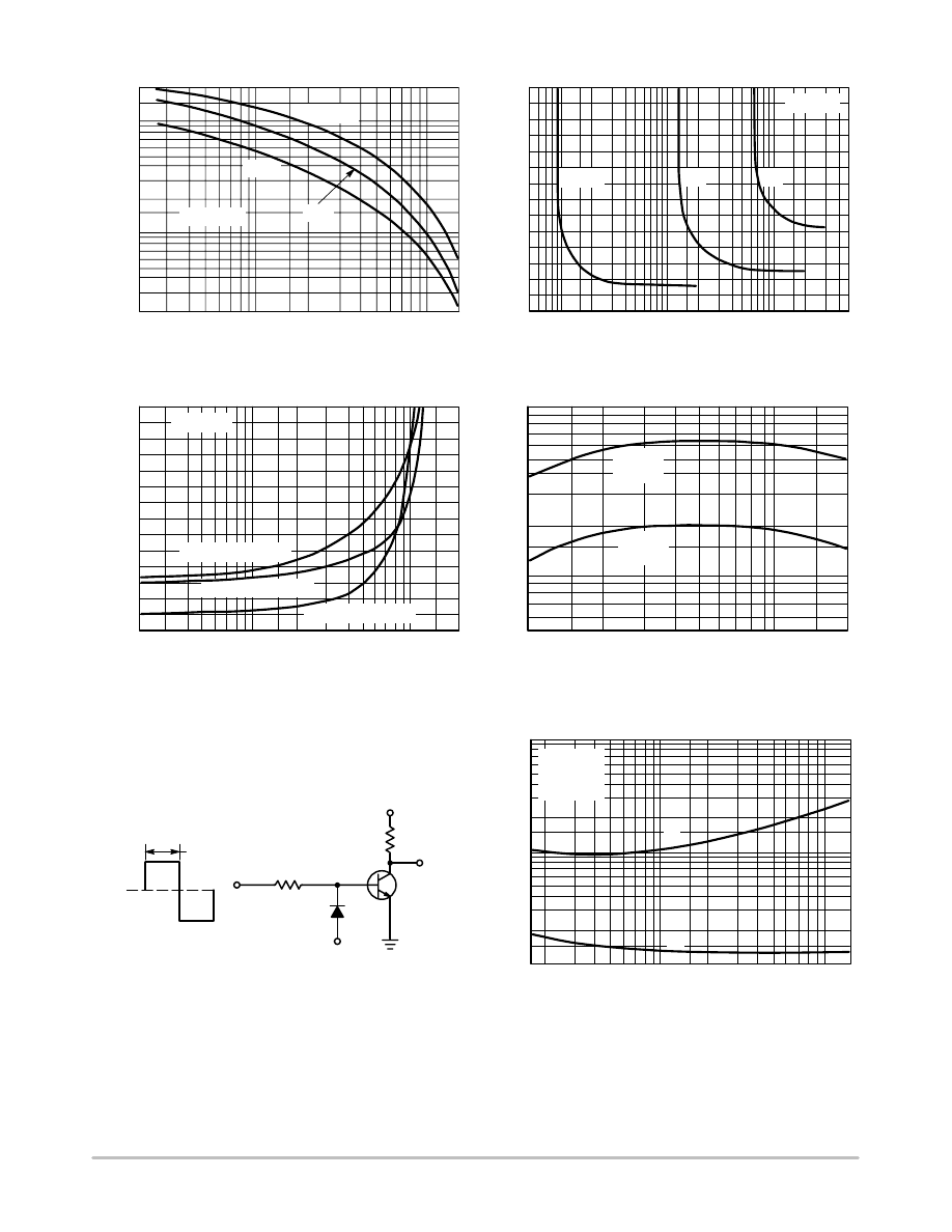
Figure 2. DC Current Gain
200
0.2
I
C
, COLLECTOR CURRENT (AMP)
2
0.3 0.5 0.7
1
2
3
5
7
15
70
30
10
5
100
50
h FE
, DC CURRENT
GAIN
T
J
= 150
°
C
25
°
C
-55
°
C
V
CE
= 4.0 V
20
7
3
10
Figure 3. Collector Saturation Region
2.8
0.005
I
B
, BASE CURRENT (AMP)
0
0.01 0.02
0.05 0.1
0.2
0.5
1
2
5
2
1.6
0.8
0.4
I
C
= 1 A
T
J
= 25
°
C
4 A
2.4
1.2
8 A
f, CURRENT-GAIN BANDWIDTH PRODUCT
(MHz)
T
3.5
0.2
I
C
, COLLECTOR CURRENT (AMP)
0.3
0.5 0.7
1
2
3
5
7
20
2.5
1.5
1
0.5
0
T
C
= 25
°
C
V
BE(sat)
@ I
C
/I
B
= 10
V
CE(sat)
@ I
C
/I
B
= 10
V,
VOL
TAGE (VOL
TS)
Figure 4. “On” Voltages
3
2
10
V
BE(on)
@ V
CE
= 4 V
10
0.1
I
C
, COLLECTOR CURRENT (AMPS)
0.2
0.3
0.5
1.0
2.0
5.0
2.0
1.0
MJ2955A
MJ15016
Figure 5. Current–Gain — Bandwidth Product
2N3055A
MJ15015
Figure 6. Switching Times Test Circuit
(Circuit shown is for NPN)
+13 V
25
µ
s
0
-11 V
30
Ω
-5 V
1N6073
SCOPE
V
CC
+30 V
7.5
Ω
t
r
, t
f
≤
10 ns
DUTY CYCLE = 1.0%
10
0.2
Figure 7. Turn–On Time
I
C
, COLLECTOR CURRENT (AMP)
t, TIME
(s)
µ
7
5
3
2
1
0.7
0.5
0.1
0.3
0.5 0.7 1
2
3
7
15
V
CC
= 30 V
I
C
/I
B
= 10
T
J
= 25
°
C
0.3
0.2
5
10
t
r
t
d
2N3055A MJ15015 MJ2955A MJ15016
http://onsemi.com
5
10
0.2
Figure 8. Turn–Off Times
I
C
, COLLECTOR CURRENT (AMPS)
7
5
3
2
0.1
0.5
0.1
0.3
0.5 0.7
1
3
5
15
V
CC
= 30
I
C
/I
B
= 10
I
B
1 = I
B
2
T
J
= 25
°
C
0.3
t, TIME
(s)
µ
t
f
t
s
2
0.7
0.2
7 10
400
1.0
Figure 9. Capacitances
V
R
, REVERSE VOLTAGE (VOLTS)
20
20
50
100 200
500 1000
2.0
5.0
10
C, CAP
ACIT
ANCE (pF)
200
100
50
30
T
J
= 25
°
C
C
ib
C
ob
2N3055A
MJ15015
MJ2955A
MJ15016
COLLECTOR CUT–OFF REGION
10,000
+0.2
Figure 10. 2N3055A, MJ15015
V
BE
, BASE-EMITTER VOLTAGE (VOLTS)
1000
100
10
1.0
, COLLECT
OR CURRENT
(A)
µ
I C 0.1
0.01
+0.1
0
-0.1
-0.2
-0.3
-0.4
-0.5
V
CE
= 30 V
T
J
= 150
°
C
100
°
C
25
°
C
REVERSE
FORWARD
I
C
= I
CES
NPN
1000
-0.2
Figure 11. MJ2955A, MJ15016
V
BE
, BASE-EMITTER VOLTAGE (VOLTS)
100
10
1.0
0.1
, COLLECT
OR CURRENT
(A)
µ
I C 0.01
0.001
-0.1
0
+0.1
+0.2
+0.3
V
CE
= 30 V
T
J
= 150
°
C
100
°
C
25
°
C
REVERSE
FORWARD
I
C
= I
CES
PNP
+0.4
+0.5
20
Figure 12. Forward Bias Safe Operating Area
2N3055A, MJ2955A
V
CE
, COLLECTOR-EMITTER VOLTAGE (VOLTS)
10
5
1
10
20
100
60
2
I C
, COLLECT
OR CURRENT
(AMPS)
dc
30
µ
s
1 ms
100
µ
s
100 ms
20
Figure 13. Forward Bias Safe Operating Area
MJ15015, MJ15016
V
CE
, COLLECTOR-EMITTER VOLTAGE (VOLTS)
10
5.0
0.2
15
20
100
60
2.0
I C
, COLLECT
OR CURRENT
(AMP)
dc
0.1ms
100ms
BONDING WIRE LIMIT
THERMAL LIMIT @ T
C
= 25
°
C
(SINGLE PULSE)
SECOND BREAKDOWN LIMIT
1.0
0.5
30
120
1.0ms
BONDING WIRE LIMIT
THERMAL LIMIT @ T
C
= 25
°
C
(SINGLE PULSE)
SECOND BREAKDOWN LIMIT

2N3055A MJ15015 MJ2955A MJ15016
http://onsemi.com
6
7
There are two limitations on the power handling ability
of a transistor: average junction temperature and second
breakdown. Safe Operating area curves indicate I
C
– V
CE
limits of the transistor that must be observed for reliable
operation; i.e., the transistor must not be subjected to greater
dissipation than the curves indicate.
The data of Figures 12 and 13 is based on T
C
= 25
C;
T
J(pk)
is variable depending on power level. Second
breakdown pulse limits are valid for duty cycles to 10% but
must be derated for temperature according to Figure 1.
2N3055A MJ15015 MJ2955A MJ15016
http://onsemi.com
7
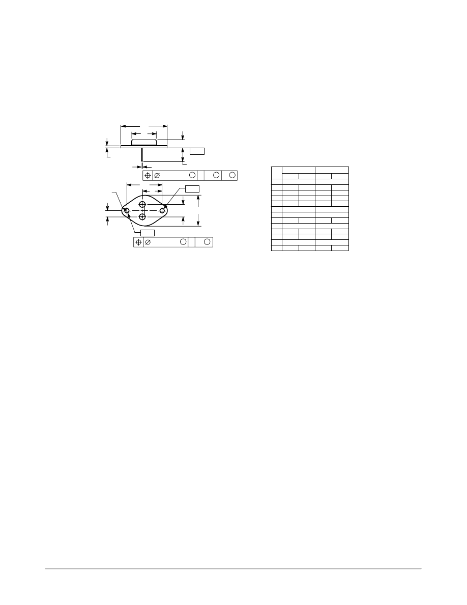
PACKAGE DIMENSIONS
NOTES:
1. DIMENSIONING AND TOLERANCING PER ANSI
Y14.5M, 1982.
2. CONTROLLING DIMENSION: INCH.
3. ALL RULES AND NOTES ASSOCIATED WITH
REFERENCED TO-204AA OUTLINE SHALL APPLY.
STYLE 1:
PIN 1. BASE
2. EMITTER
CASE: COLLECTOR
DIM
MIN
MAX
MIN
MAX
MILLIMETERS
INCHES
A
1.550 REF
39.37 REF
B
---
1.050
---
26.67
C
0.250
0.335
6.35
8.51
D
0.038
0.043
0.97
1.09
E
0.055
0.070
1.40
1.77
G
0.430 BSC
10.92 BSC
H
0.215 BSC
5.46 BSC
K
0.440
0.480
11.18
12.19
L
0.665 BSC
16.89 BSC
N
---
0.830
---
21.08
Q
0.151
0.165
3.84
4.19
U
1.187 BSC
30.15 BSC
V
0.131
0.188
3.33
4.77
A
N
E
C
K
–T–
SEATING
PLANE
2 PL
D
M
Q
M
0.13 (0.005)
Y
M
T
M
Y
M
0.13 (0.005)
T
–Q–
–Y–
2
1
U
L
G
B
V
H
CASE 1–07
TO–204AA (TO–3)
ISSUE Z

2N3055A MJ15015 MJ2955A MJ15016
http://onsemi.com
8
ON Semiconductor and are trademarks of Semiconductor Components Industries, LLC (SCILLC). SCILLC reserves the right to make changes
without further notice to any products herein. SCILLC makes no warranty, representation or guarantee regarding the suitability of its products for any particular
purpose, nor does SCILLC assume any liability arising out of the application or use of any product or circuit, and specifically disclaims any and all liability,
including without limitation special, consequential or incidental damages. “Typical” parameters which may be provided in SCILLC data sheets and/or
specifications can and do vary in different applications and actual performance may vary over time. All operating parameters, including “Typicals” must be
validated for each customer application by customer’s technical experts. SCILLC does not convey any license under its patent rights nor the rights of others.
SCILLC products are not designed, intended, or authorized for use as components in systems intended for surgical implant into the body, or other applications
intended to support or sustain life, or for any other application in which the failure of the SCILLC product could create a situation where personal injury or
death may occur. Should Buyer purchase or use SCILLC products for any such unintended or unauthorized application, Buyer shall indemnify and hold
SCILLC and its officers, employees, subsidiaries, affiliates, and distributors harmless against all claims, costs, damages, and expenses, and reasonable
attorney fees arising out of, directly or indirectly, any claim of personal injury or death associated with such unintended or unauthorized use, even if such claim
alleges that SCILLC was negligent regarding the design or manufacture of the part. SCILLC is an Equal Opportunity/Affirmative Action Employer.
PUBLICATION ORDERING INFORMATION
CENTRAL/SOUTH AMERICA:
Spanish Phone: 303–308–7143 (Mon–Fri 8:00am to 5:00pm MST)
Email: ONlit–spanish@hibbertco.com
Toll–Free from Mexico: Dial 01–800–288–2872 for Access –
then Dial 866–297–9322
ASIA/PACIFIC: LDC for ON Semiconductor – Asia Support
Phone: 1–303–675–2121 (Tue–Fri 9:00am to 1:00pm, Hong Kong Time)
Toll Free from Hong Kong & Singapore:
001–800–4422–3781
Email: ONlit–asia@hibbertco.com
JAPAN: ON Semiconductor, Japan Customer Focus Center
4–32–1 Nishi–Gotanda, Shinagawa–ku, Tokyo, Japan 141–0031
Phone: 81–3–5740–2700
Email: r14525@onsemi.com
ON Semiconductor Website: http://onsemi.com
For additional information, please contact your local
Sales Representative.
2N3055A/D
PowerBase is a trademark of Semiconductor Components Industries, LLC.
NORTH AMERICA Literature Fulfillment:
Literature Distribution Center for ON Semiconductor
P.O. Box 5163, Denver, Colorado 80217 USA
Phone: 303–675–2175 or 800–344–3860 Toll Free USA/Canada
Fax: 303–675–2176 or 800–344–3867 Toll Free USA/Canada
Email: ONlit@hibbertco.com
Fax Response Line: 303–675–2167 or 800–344–3810 Toll Free USA/Canada
N. American Technical Support: 800–282–9855 Toll Free USA/Canada
EUROPE: LDC for ON Semiconductor – European Support
German Phone: (+1) 303–308–7140 (Mon–Fri 2:30pm to 7:00pm CET)
Email: ONlit–german@hibbertco.com
French Phone: (+1) 303–308–7141 (Mon–Fri 2:00pm to 7:00pm CET)
Email: ONlit–french@hibbertco.com
English Phone: (+1) 303–308–7142 (Mon–Fri 12:00pm to 5:00pm GMT)
Email: ONlit@hibbertco.com
EUROPEAN TOLL–FREE ACCESS*: 00–800–4422–3781
*Available from Germany, France, Italy, UK, Ireland
Wyszukiwarka
Podobne podstrony:
2N3055, MJ2955 (ON Semiconductor)
2N3055A, MJ15015, MJ2955A, MJ15016 (Motorola)
2N7000 (ON Semiconductor)
BTB16 (ON Semiconductor)
BF256 (ON Semiconductor)
BTA16 (ON Semiconductor)
BC337, BC338 (ON Semiconductor)
TIP131, TIP132, TIP137 (ON Semiconductor)
BC327, BC328 (ON Semiconductor)
MCR69 (ON Semiconductor)
MPSA13, MPSA14 (ON Semiconductor)
BS108 (ON Semiconductors)
2N3055 MJ2955
2N3055, MJ2955 (Motorola)
2N3055, MJ2955 (STMicroelectronics)
More on hypothesis testing
ZPSBN T 24 ON poprawiony
KIM ON JEST2
więcej podobnych podstron