Semiconductor Components Industries, LLC, 2004
December, 2004 − Rev. 1
1
Publication Order Number:
MCR69/D
MCR69−2, MCR69−3
Silicon Controlled Rectifiers
Reverse Blocking Thyristors
Designed for overvoltage protection in crowbar circuits.
Features
•
Glass-Passivated Junctions for Greater Parameter Stability and
Reliability
•
Center-Gate Geometry for Uniform Current Spreading Enabling
High Discharge Current
•
Small Rugged, Thermowatt Package Constructed for Low Thermal
Resistance and Maximum Power Dissipation and Durability
•
High Capacitor Discharge Current, 750 Amps
•
Pb−Free Packages are Available*
MAXIMUM RATINGS
(T
J
= 25
°
C unless otherwise noted)
Rating
Symbol
Value
Unit
Peak Repetitive Off−State Voltage (Note 1)
(T
J
=
40 to +125
°
C, Gate Open)
MCR69−2
MCR69−3
V
DRM,
V
RRM
50
100
V
Peak Discharge Current (Note 2)
I
TM
750
A
On-State RMS Current
(180
°
Conduction Angles; T
C
= 85
°
C)
I
T(RMS)
25
A
Average On-State Current
(180
°
Conduction Angles; T
C
= 85
°
C)
I
T(AV)
16
A
Peak Non-Repetitive Surge Current
(1/2 Cycle, Sine Wave, 60 Hz, T
J
= 125
°
C)
I
TSM
300
A
Circuit Fusing Considerations (t = 8.3 ms)
I
2
t
375
A
2
s
Forward Peak Gate Current
(t
≤
1.0
s, T
C
= 85
°
C)
I
GM
2.0
A
Forward Peak Gate Power
(t
≤
1.0
s, T
C
= 85
°
C)
P
GM
20
W
Forward Average Gate Power
(t = 8.3 ms, T
C
= 85
°
C)
P
G(AV)
0.5
W
Operating Junction Temperature Range
T
J
−40 to +125
°
C
Storage Temperature Range
T
stg
−40 to +150
°
C
Mounting Torque
−
8.0
in. lb.
Maximum ratings are those values beyond which device damage can occur.
Maximum ratings applied to the device are individual stress limit values (not
normal operating conditions) and are not valid simultaneously. If these limits
are exceeded, device functional operation is not implied, damage may occur
and reliability may be affected.
1. V
DRM
and V
RRM
for all types can be applied on a continuous basis. Ratings
apply for zero or negative gate voltage; however, positive gate voltage shall
not be applied concurrent with negative potential on the anode. Blocking
voltages shall not be tested with a constant current source such that the
voltage ratings of the devices are exceeded.
2. Ratings apply for t
w
= 1 ms. See Figure 1 for I
TM
capability for various
duration of an exponentially decaying current waveform, t
w
is defined as
5 time constants of an exponentially decaying current pulse.
3. Test Conditions: I
G
= 150 mA, V
D
= Rated V
DRM
, I
TM
= Rated Value, T
J
= 125
°
C.
*For additional information on our Pb−Free strategy and soldering details, please
download the ON Semiconductor Soldering and Mounting Techniques
Reference Manual, SOLDERRM/D.
SCRs
25 AMPERES RMS
50 thru 100 VOLTS
Device
Package
Shipping
†
ORDERING INFORMATION
MCR69−2
TO220AB
500/Box
K
G
A
TO−220AB
CASE 221A
STYLE 3
1
2
3
4
PIN ASSIGNMENT
1
2
3
Anode
Gate
Cathode
4
Anode
MCR69−3
TO220AB
500/Box
MCR69−3G
TO220AB
(Pb−Free)
500/Box
MCR69−2G
TO220AB
(Pb−Free)
500/Box
†For information on tape and reel specifications,
including part orientation and tape sizes, please
refer to our Tape and Reel Packaging Specifications
Brochure, BRD8011/D.
http://onsemi.com
MARKING
DIAGRAM
MCR69x
A
= Assembly Location
Y
= Year
WW
= Work Week
MCR69 = Device Code
x
= 2 or 3
AKA
= Location Code
AKA
AYWW
MCR69−2, MCR69−3
http://onsemi.com
2
THERMAL CHARACTERISTICS
Characteristic
Symbol
Max
Unit
Thermal Resistance, Junction−to−Case
R
JC
1.5
°
C/W
Thermal Resistance, Junction−to−Ambient
R
JA
60
°
C/W
Maximum Lead Temperature for Soldering Purposes 1/8 in from Case for 10 Seconds
T
L
260
°
C
ELECTRICAL CHARACTERISTICS
(T
C
= 25
°
C unless otherwise noted.)
Characteristic
Symbol
Min
Typ
Max
Unit
OFF CHARACTERISTICS
Peak Repetitive Forward or Reverse Blocking Current
(V
AK
= Rated V
DRM
or V
RRM
, Gate Open)
T
J
= 25
°
C
T
J
= 125
°
C
I
DRM
, I
RRM
−
−
−
−
10
2.0
A
mA
ON CHARACTERISTICS
Peak Forward On-State Voltage
(I
TM
= 50 A) (Note 4)
(I
TM
= 750 A, t
w
= 1 ms) (Note 5)
V
TM
−
−
−
6.0
1.8
−
V
Gate Trigger Current (Continuous dc)
(V
D
= 12 V, R
L
= 100
)
I
GT
2.0
7.0
30
mA
Gate Trigger Voltage (Continuous dc)
(V
D
= 12 V, R
L
= 100
)
V
GT
−
0.65
1.5
V
Gate Non−Trigger Voltage
(V
D
= 12 Vdc, R
L
= 100
, T
J
= 125
°
C)
V
GD
0.2
0.40
−
V
Holding Current
(V
D
= 12 V, Initiating Current = 200 mA, Gate Open)
I
H
3.0
15
50
mA
Latching Current
(V
D
= 12 Vdc, I
G
= 150 mA)
I
L
−
−
60
mA
Gate Controlled Turn-On Time (Note 6)
(V
D
= Rated V
DRM
, I
G
= 150 mA)
(I
TM
= 50 A Peak)
t
gt
−
1.0
−
s
DYNAMIC CHARACTERISTICS
Critical Rate-of-Rise of Off-State Voltage
(V
D
= Rated V
DRM
, Gate Open, Exponential Waveform, T
J
= 125
°
C)
dv/dt
10
−
−
V/
s
Critical Rate-of-Rise of On-State Current
I
G
= 150 mA
T
J
= 125
°
C
di/dt
−
−
100
A/
s
4. Pulse duration
300
s, duty cycle
2%.
5. Ratings apply for t
w
= 1 ms. See Figure 1 for I
TM
capability for various durations of an exponentially decaying current waveform. t
w
is defined
as 5 time constants of an exponentially decaying current pulse.
6. The gate controlled turn-on time in a crowbar circuit will be influenced by the circuit inductance.
MCR69−2, MCR69−3
http://onsemi.com
3
+ Current
+ Voltage
V
TM
I
DRM
at V
DRM
I
H
Symbol
Parameter
V
DRM
Peak Repetitive Off State Forward Voltage
I
DRM
Peak Forward Blocking Current
V
RRM
Peak Repetitive Off State Reverse Voltage
I
RRM
Peak Reverse Blocking Current
V
TM
Peak On State Voltage
I
H
Holding Current
Voltage Current Characteristic of SCR
Anode +
on state
Reverse Blocking Region
(off state)
Reverse Avalanche Region
Anode −
Forward Blocking Region
I
RRM
at V
RRM
(off state)
NORMALIZED PEAK CURRENT
0.8
25
0
0.2
0.4
0.6
1.0
50
75
100
125
T
C
, CASE TEMPERATURE (
°
C)
Figure 1. Peak Capacitor Discharge Current
Figure 2. Peak Capacitor Discharge Current
Derating
Figure 3. Current Derating
Figure 4. Maximum Power Dissipation
I , PEAK DISCHARGE CURRENT
(AMPS)
TM
300
20
50
100
200
20
1000
0.5
50
t
w
, PULSE CURRENT DURATION (ms)
2.0
1.0
t
w
t
w
= 5 time constants
I
TM
10
5.0
T , MAXIMUM
ALLOW
ABLE
C
CASE
TEMPERA
TURE ( C)
°
16
20
12
4.0
8.0
dc
Half Wave
75
80
85
90
95
100
105
110
115
120
125
I
T(AV)
, AVERAGE ON-STATE CURRENT (AMPS)
P ,
AVERAGE POWER DISSIP
ATION (W
ATTS)
(A
V)
16
12
8.0
4.0
0
24
16
8.0
32
0
20
Half Wave
dc
I
T(AV)
, AVERAGE ON-STATE CURRENT (AMPS)
T
J
= 125
°
C
MCR69−2, MCR69−3
http://onsemi.com
4
2 k
10 k
5 k
3 k
10
t, TIME (ms)
1 k
500
300
200
100
50
30
0.2
20
1
0.7
0.5
0.1
0.2
0.02
5
2
3
1
0.5
0.3
0.1
0.3
0.07
0.05
0.03
0.01
Z
JC(t)
= R
JC
•
r(t)
r(t), TRANSIENT
THERMAL
RESIST
ANCE
(NORMALIZED)
Figure 5. Thermal Response
NORMALIZED GA
TE
TRIGGER CURRENT
NORMALIZED GA
TE
TRIGGER VOL
TAGE
NORMALIZED HOLD CURRENT
−40
10
0.2
0.3
140
120
100
80
60
40
−20
0
20
0.5
1.2
1.0
0.8
−40
−60
1.4
T
J
, JUNCTION TEMPERATURE (
°
C)
40
0
20
60
0.5
3.0
5.0
140
80
100
120
2.0
1.0
−20
−60
T
J
, JUNCTION TEMPERATURE (
°
C)
V
D
= 12 Volts
R
L
= 100
V
D
= 12 Volts
R
L
= 100
0.3
0.5
0.8
1.0
140
120
40
100
3.0
2.0
20
60
80
0
−40
T
J
, JUNCTION TEMPERATURE (
°
C)
−20
−60
V
D
= 12 Volts
I
TM
= 100 mA
Figure 6. Gate Trigger Current
Figure 7. Gate Trigger Voltage
Figure 8. Holding Current
MCR69−2, MCR69−3
http://onsemi.com
5
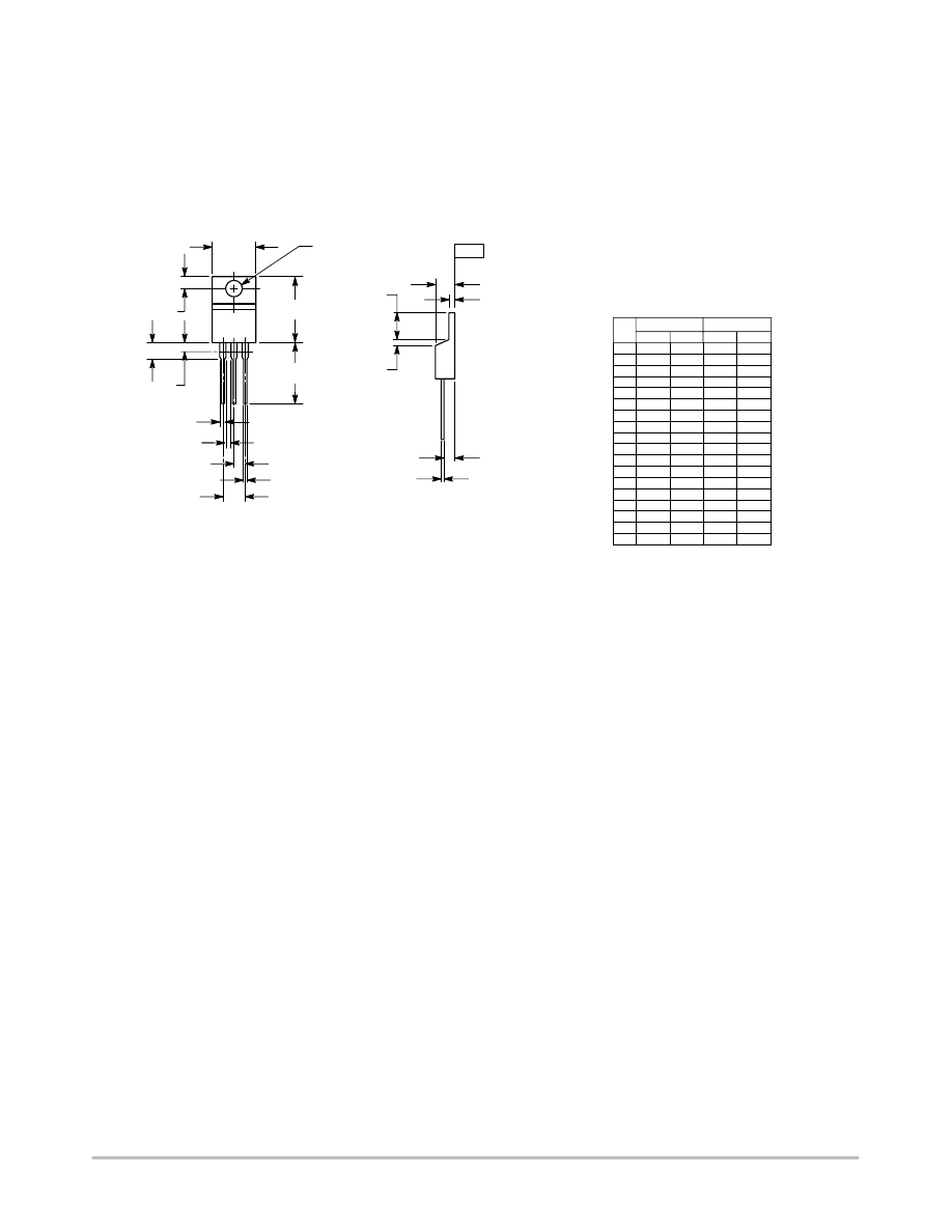
PACKAGE DIMENSIONS
TO−220AB
CASE 221A−07
ISSUE AA
STYLE 3:
PIN 1. CATHODE
2. ANODE
3. GATE
4. ANODE
NOTES:
1. DIMENSIONING AND TOLERANCING PER ANSI
Y14.5M, 1982.
2. CONTROLLING DIMENSION: INCH.
3. DIMENSION Z DEFINES A ZONE WHERE ALL
BODY AND LEAD IRREGULARITIES ARE
ALLOWED.
DIM
MIN
MAX
MIN
MAX
MILLIMETERS
INCHES
A
0.570
0.620
14.48
15.75
B
0.380
0.405
9.66
10.28
C
0.160
0.190
4.07
4.82
D
0.025
0.035
0.64
0.88
F
0.142
0.147
3.61
3.73
G
0.095
0.105
2.42
2.66
H
0.110
0.155
2.80
3.93
J
0.014
0.022
0.36
0.55
K
0.500
0.562
12.70
14.27
L
0.045
0.060
1.15
1.52
N
0.190
0.210
4.83
5.33
Q
0.100
0.120
2.54
3.04
R
0.080
0.110
2.04
2.79
S
0.045
0.055
1.15
1.39
T
0.235
0.255
5.97
6.47
U
0.000
0.050
0.00
1.27
V
0.045
−−−
1.15
−−−
Z
−−−
0.080
−−−
2.04
A
K
L
V
G
D
N
Z
H
Q
F
B
1 2 3
4
−T−
SEATING
PLANE
S
R
J
U
T
C

MCR69−2, MCR69−3
http://onsemi.com
6
ON Semiconductor and are registered trademarks of Semiconductor Components Industries, LLC (SCILLC). SCILLC reserves the right to make changes without further notice
to any products herein. SCILLC makes no warranty, representation or guarantee regarding the suitability of its products for any particular purpose, nor does SCILLC assume any liability
arising out of the application or use of any product or circuit, and specifically disclaims any and all liability, including without limitation special, consequential or incidental damages.
“Typical” parameters which may be provided in SCILLC data sheets and/or specifications can and do vary in different applications and actual performance may vary over time. All
operating parameters, including “Typicals” must be validated for each customer application by customer’s technical experts. SCILLC does not convey any license under its patent rights
nor the rights of others. SCILLC products are not designed, intended, or authorized for use as components in systems intended for surgical implant into the body, or other applications
intended to support or sustain life, or for any other application in which the failure of the SCILLC product could create a situation where personal injury or death may occur. Should
Buyer purchase or use SCILLC products for any such unintended or unauthorized application, Buyer shall indemnify and hold SCILLC and its officers, employees, subsidiaries, affiliates,
and distributors harmless against all claims, costs, damages, and expenses, and reasonable attorney fees arising out of, directly or indirectly, any claim of personal injury or death
associated with such unintended or unauthorized use, even if such claim alleges that SCILLC was negligent regarding the design or manufacture of the part. SCILLC is an Equal
Opportunity/Affirmative Action Employer. This literature is subject to all applicable copyright laws and is not for resale in any manner.
PUBLICATION ORDERING INFORMATION
N. American Technical Support: 800−282−9855 Toll Free
USA/Canada
Japan: ON Semiconductor, Japan Customer Focus Center
2−9−1 Kamimeguro, Meguro−ku, Tokyo, Japan 153−0051
Phone: 81−3−5773−3850
MCR69/D
LITERATURE FULFILLMENT:
Literature Distribution Center for ON Semiconductor
P.O. Box 61312, Phoenix, Arizona 85082−1312 USA
Phone: 480−829−7710 or 800−344−3860 Toll Free USA/Canada
Fax: 480−829−7709 or 800−344−3867 Toll Free USA/Canada
Email: orderlit@onsemi.com
ON Semiconductor Website: http://onsemi.com
Order Literature: http://www.onsemi.com/litorder
For additional information, please contact your
local Sales Representative.
Wyszukiwarka
Podobne podstrony:
2N7000 (ON Semiconductor)
BTB16 (ON Semiconductor)
2N3055, MJ2955 (ON Semiconductor)
BF256 (ON Semiconductor)
BTA16 (ON Semiconductor)
BC337, BC338 (ON Semiconductor)
TIP131, TIP132, TIP137 (ON Semiconductor)
BC327, BC328 (ON Semiconductor)
2N3055A, MJ15015, MJ2955A, MJ15016 (ON Semiconductor)
MPSA13, MPSA14 (ON Semiconductor)
BS108 (ON Semiconductors)
More on hypothesis testing
ZPSBN T 24 ON poprawiony
KIM ON JEST2
Parzuchowski, Purek ON THE DYNAMIC
Foucault On Kant
G B Folland Lectures on Partial Differential Equations
free sap tutorial on goods reciept
5th Fábos Conference on Landscape and Greenway Planning 2016
więcej podobnych podstron