V772 CRT Monitor Service Guide
Circuit Operation Theory
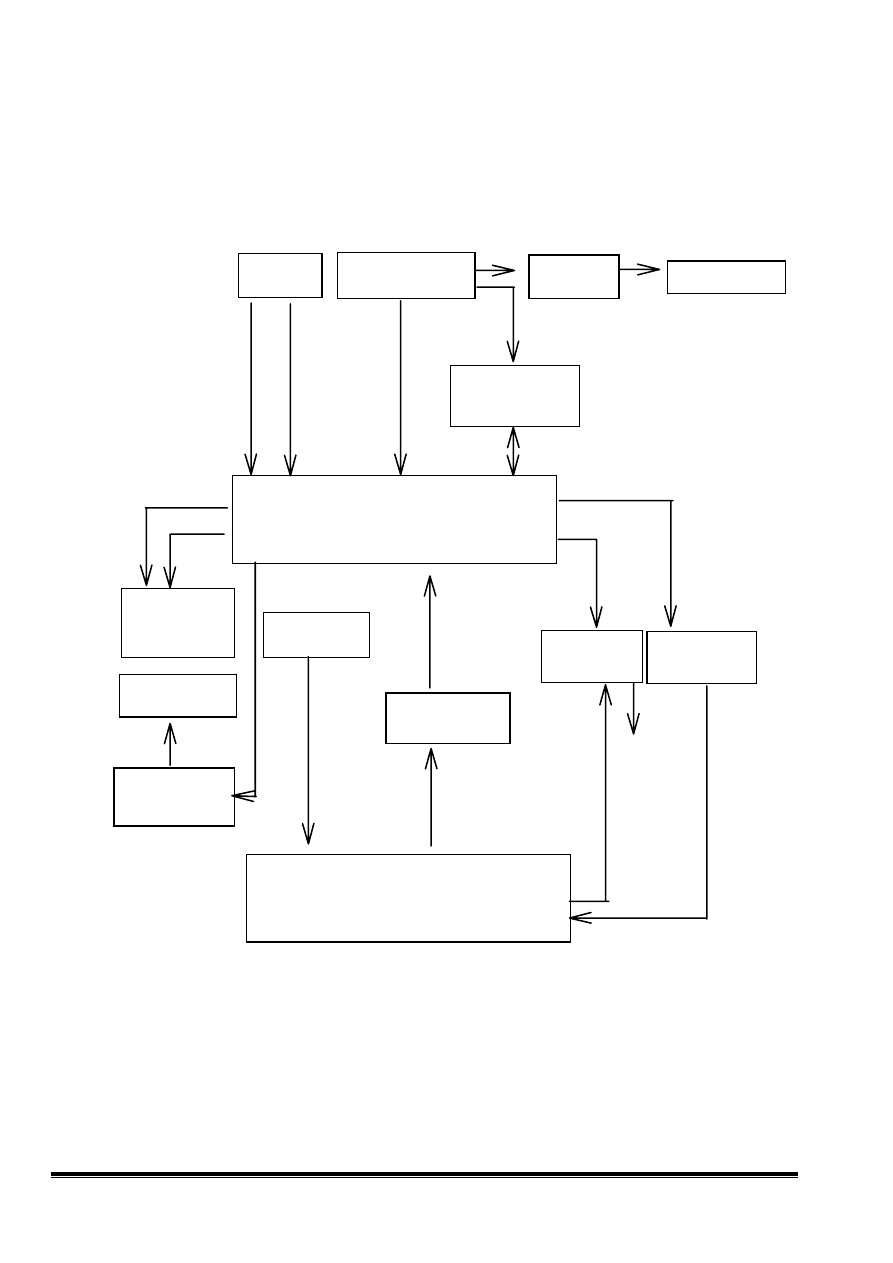
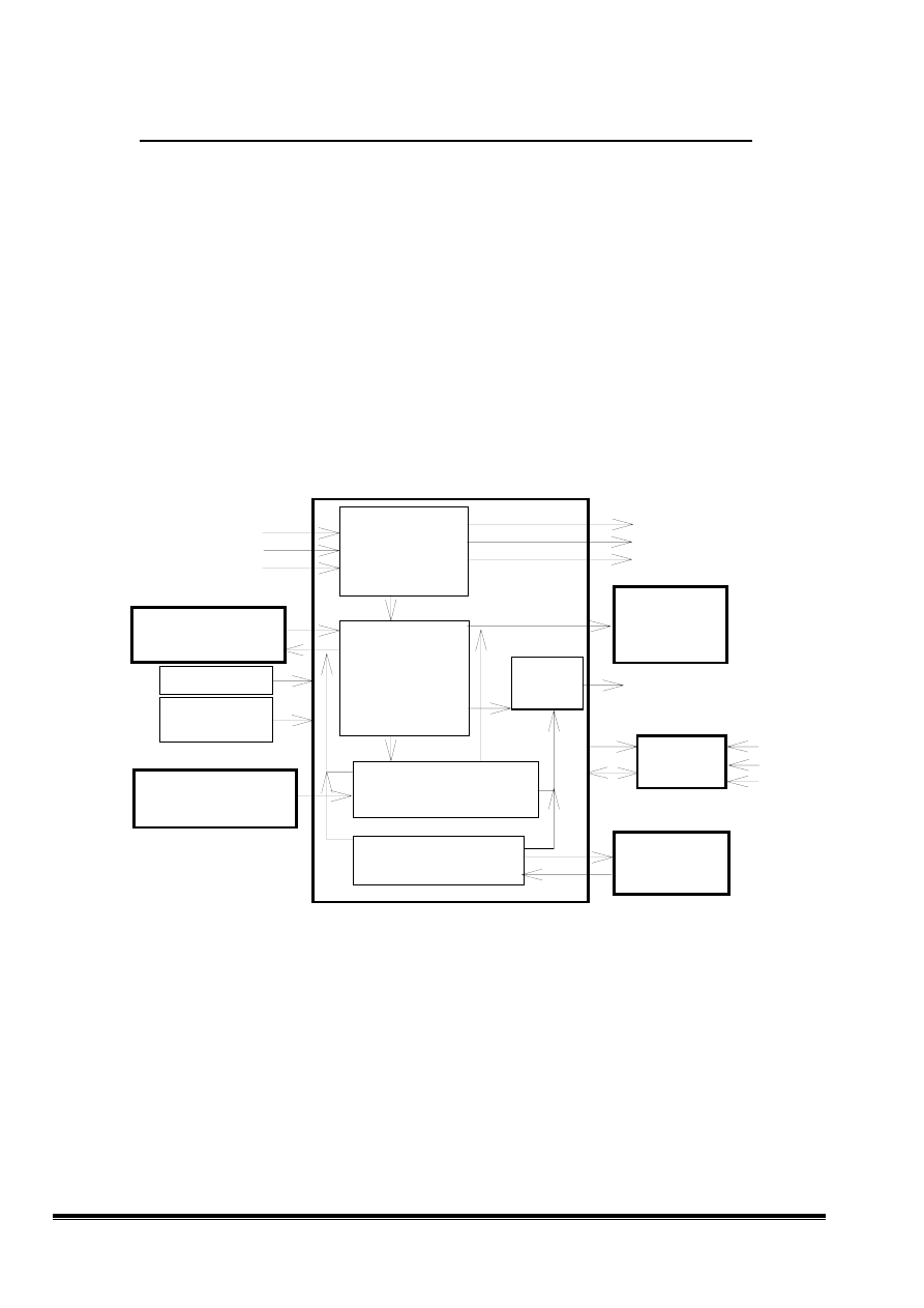
ACER V772 DEFLECTION CIRCUIT OPERATION THEORY
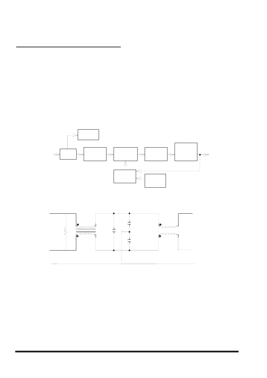
1. The Block Diagram of Deflection:
H-sync
V-sync
Digital
Controller
Tilt
Circuit
Rotation
C il
I2C BUS
AutoSync Deflection
Controller
IC TDA4856
Vertical
Deflection
Output
IC TDA4866
H-SIZE
Compensation
Dynamic
Regulation
Feedback
Step Up
for B+
Horizontal
Deflection Output
Circuit
Shut down
Circuit
G1 & Spot
Killer Circuit
Dynamic
Focus
G1
1
Confidential
V772 CRT Monitor Service Guide
Circuit Operation Theory
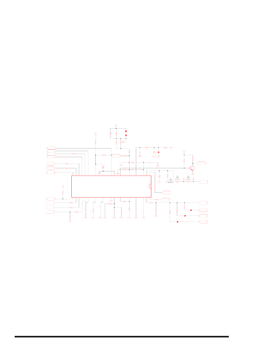
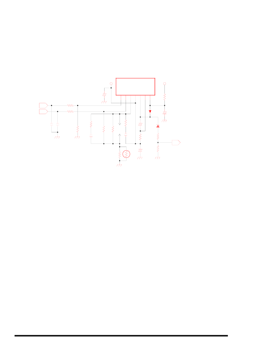
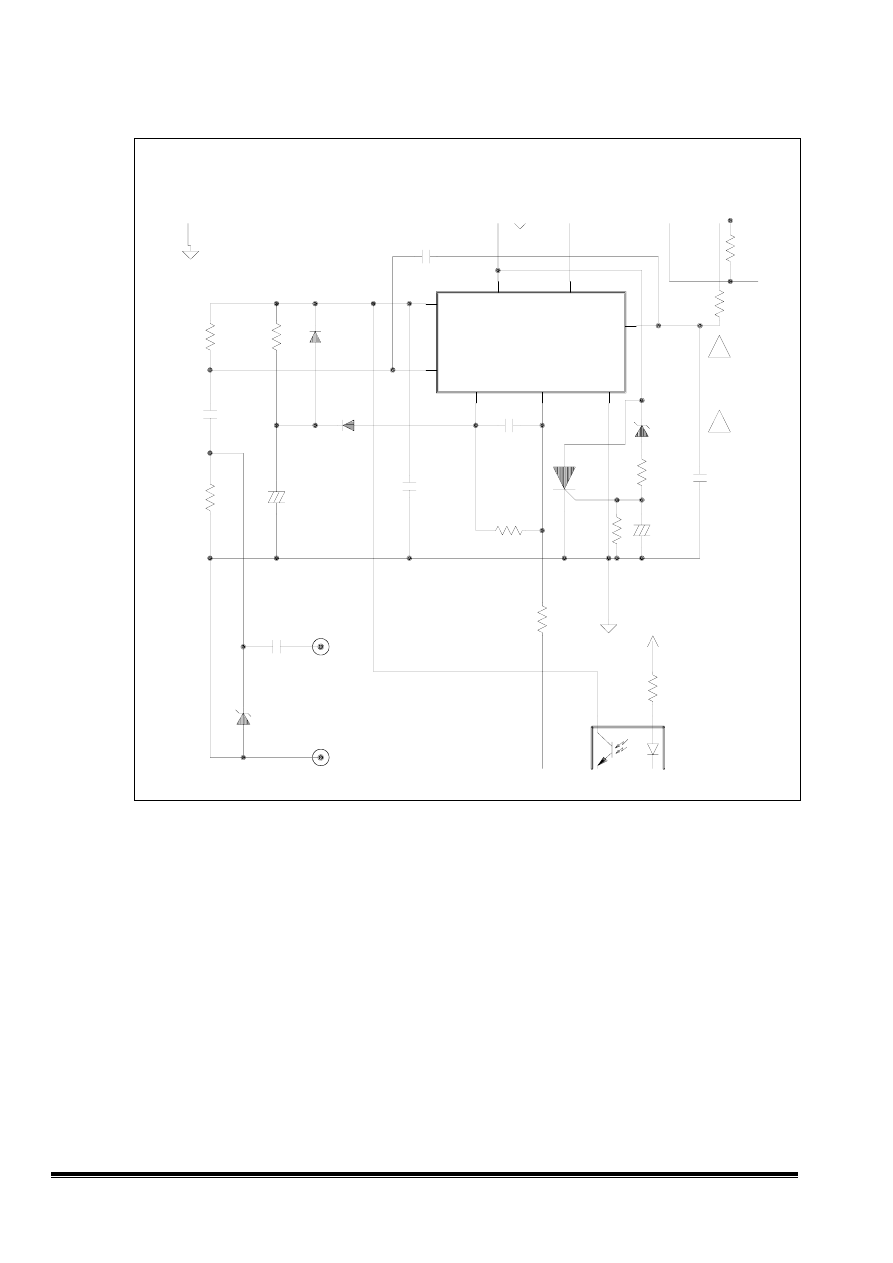
2. Autosync Deflection Controller (TDA4856)
2.1 pin 1 is AFC feedback.
2.2 pin XRAY: if V XRAY > threshold (6.25V typical) switches the whole IC into protection mode.
2.3 pin 3,4,5,6,8 for B+ control function block.
2.4 pin 11(EWDRV) is a parabolic waveform used for pincushion correction
2.5 pin 16 generates video claming & blanking pulse.
2.6 pin 18,19 is I2C data.
2.7 pin 21 V-regulation.
2.8 the resistor from pin 28 (HREF) to ground determines the maximum oscillator frequency.
2.9 the resistor from pin 27 (HBUF) to pin 28 defines the frequency range.
2.10 pin 31 H-regulation.
2.11 pin 32 focus.
D201
R237
R268
C205
R266
R267
R263
C207
R205
R236
C202
C210
C208
VR201
C206
IC201
R260
R222
R221
R204
R220
R211
R202
R201
R213
R209
R210
D207
R206
R218
R217
R216
R215
R214
R212
R258
C222
C201
C204
Q201
C211
C209
ZD204
R208
R264
R265
R235
ZD201
R257
R238
C226
C203
C227
R203
R262
R270
R261
D208
D206
1N4148
10K
120K
50V
2.2U
(EL)
8.2M
56K
1K
100V
0.1U
(PE)
110K
(FS)
1/2W
10
100V
0.01U
(PE)
100V
0.01U
(EPI)
100V
0.1U
(PE)
(OPEN)
HVADJ
100V
0.1U
(PE)
TDA4856
390K
1/4W
4.7K
10K
1/4W
2.2K
JUMPER
JUMPER
100
100
3.3K
100
100
1N4148
JUMPER
22.1K
(1%)
100K
(1%)
15.8K
(1%)
2.67K
(1%)
1.27K
(1%)
22.1K
(1%)
(OPEN)
50V
1U
(EL)
50V
47U
(EL)
50V
2.2U
(EL)
H945
100V
2200P
(PE)
100V
8200P
(PE)
30V
1M
100
100
10K
12V
2.2K
12K
25V
100U
(EL)
100V
2200P
(PE)
50V
0.1U
(D)
62K
(OPEN)
10K
(OPEN)
(OPEN)
(OPEN)
V1
V2
HFLB
EWDRV
PWM
HDRV
FOCUS
FOCUS
CLAMP
VBL
SC0
SC2
HV-ADJ
HBL
HULK
SC1
HSMOD
SDA
+14V
+14V
+14V
+14V
+48V
+48V
SCL
VSMOD
TP3
TP2
+
GND
HPLL2
HSMOD
FOCUS
SGND
VSMOD
ASCOR
SDA
SCL
HUNLOCK
VCC
i.c.
BDRV
HFLB
32
31
30
29
28
27
26
25
24
23
22
21
20
19
18
17
CLBL
HSYNC
VSYNC
VOUT1
VOUT2
EWDRV
VAGC
VCAP
VREF
HPLL1
HBUF
HREF
HCAP
HDRV
BIN
BSENS
BOP
XRAY
16
15
14
13
12
11
10
9
8
7
6
5
4
3
2
1
+
+
+
+
Fig 2 Autosync Deflection Controller circuit
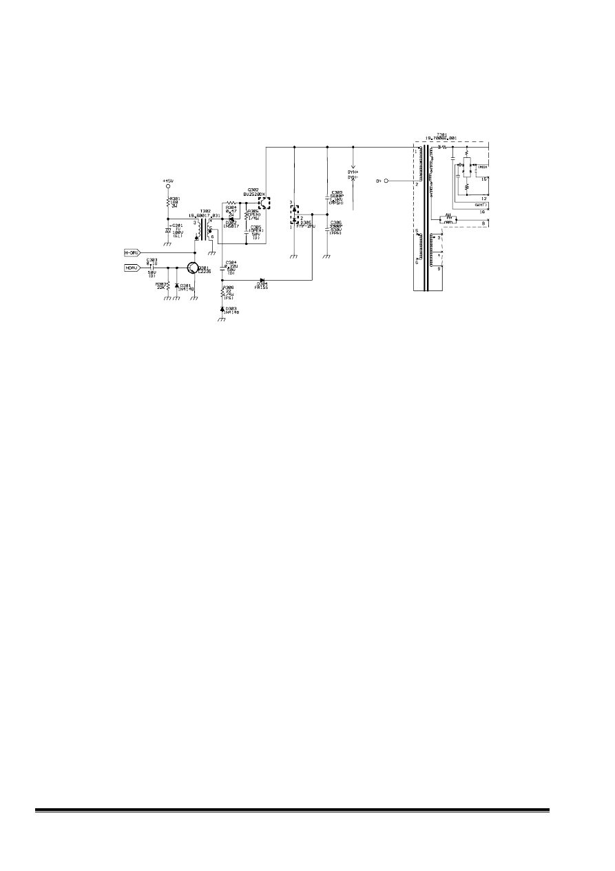
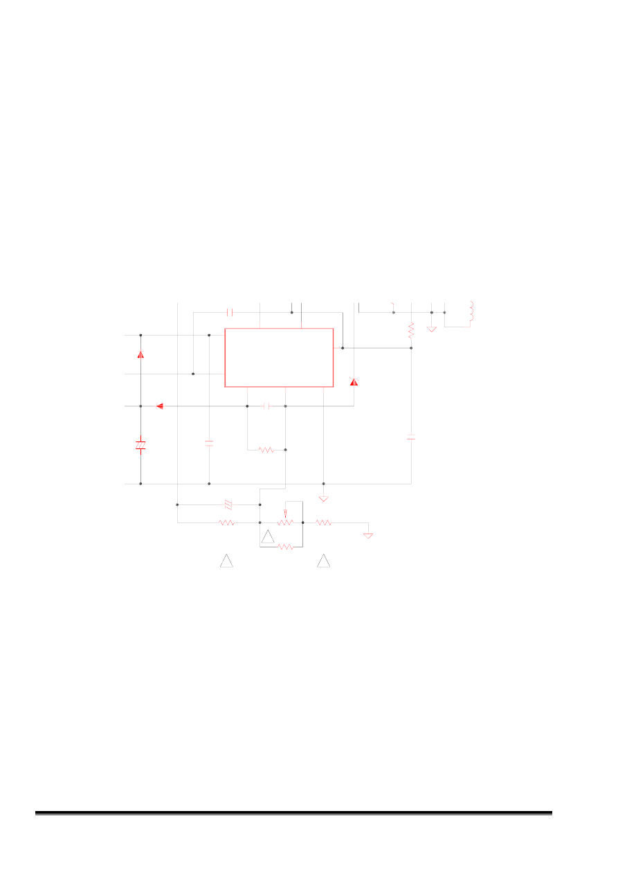
3. H-Driver & Output CKT:
3.1 HDRV signal comes from IC201 pin8, then goes into Q301, Q301 constitutes an inverting stage
and combines with T302 to drive Q302.
3.2 Q302, C306, C309, D305 constitute the H-output CKT with diode modulator mode.
3.3 Q324 & Q325 constitute a switch for lower frequency driver switching to cover the low h
fe
HOT
running under low frequency will occur poor-drive condition.
2
Confidential
V772 CRT Monitor Service Guide
Circuit Operation Theory
Fig 3 HDRV & output circuit
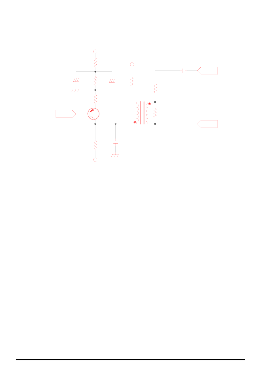
4. Dynamic focus CKT
According to the CRT spec
H dynamic focus Vpp = 300 V
V dynamic focus Vpp = 130 V
4-1 Vertical dynamic focus
The signal from IC201 (pin 32) is a vertical frequency parabolic waveform.
Q321: an inverting amplifier stage.
4-2 Horizontal dynamic focus:
The waveform of C313 (CS-2, CS-1) is a horizontal frequency parabolic waveform, and is amplified by
T304.
3
Confidential
V772 CRT Monitor Service Guide
Circuit Operation Theory
C346
R391
R373
R379
R327
T304
Q321
C328
C327
C329
R351
R352
R353
16V
22U
(EL)
1K
1/2W
150
2W
1K
(FS)
1W
10
19.20113.001
BF423
(D)
1KV
470P
50V
10U
(EL)
400V
0.033U
(MPE)
68K
3.9K
1/4W
560K
FOCUS
-190V
DAF
CS-2
CS-1
+14V
+
3
4
1
2
+
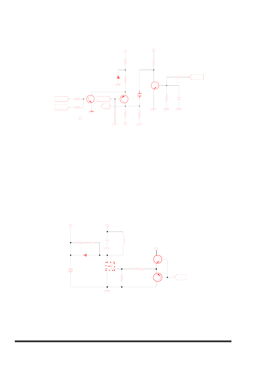
5. Brightness & spot killer CKT.
Fig 4 Dynamic Focus circuit
5.1 G1 CKT
The bright control signal from UC controller is about 0 ~ 5V, when the voltage of bright control signal
decreases, the current flow through R241 increases and the voltage of G1 increases.
5.2 Blanking CKT
To avoid the disturbed picture display on the screen, we have to blank the monitor in the following
situations.
(1) when display mode is changed.
(2) when the monitor enter the power saving mode.
(3) blank the vertical retrace line
when the " blank" signal becomes "high" Q208 "ON" , Q203 "OFF".G1 voltage is about ( -190 *
R271/(R271+R241)) ≒ -184V. The signal which is IC201 (pin 16) is inverted and amplified by Q202,
and coupling to G1.During the vertical retrace interval , the G1 voltage will be drop down about 48V.
4
Confidential
V772 CRT Monitor Service Guide
Circuit Operation Theory
R271
R232
ZD203
R254
R255
C223
Q203
R239
R241
Q202
R240
R231
Q208
R256
C224
R269
1/2W
1M
1/2W
5.6K
5.1V
2.7K
10K
(D)
50V
0.01U
BF423
6.8K
1/2W
100K
H945
3.3K
1/4W
100
H945
10K
250V
0.22U
(EL)
1K
+45V
BRITE
-190V
CLAMP
HULK
BLANK
+6.5V
G1
+
+
Fig5 Brightness & Spot killer circuit
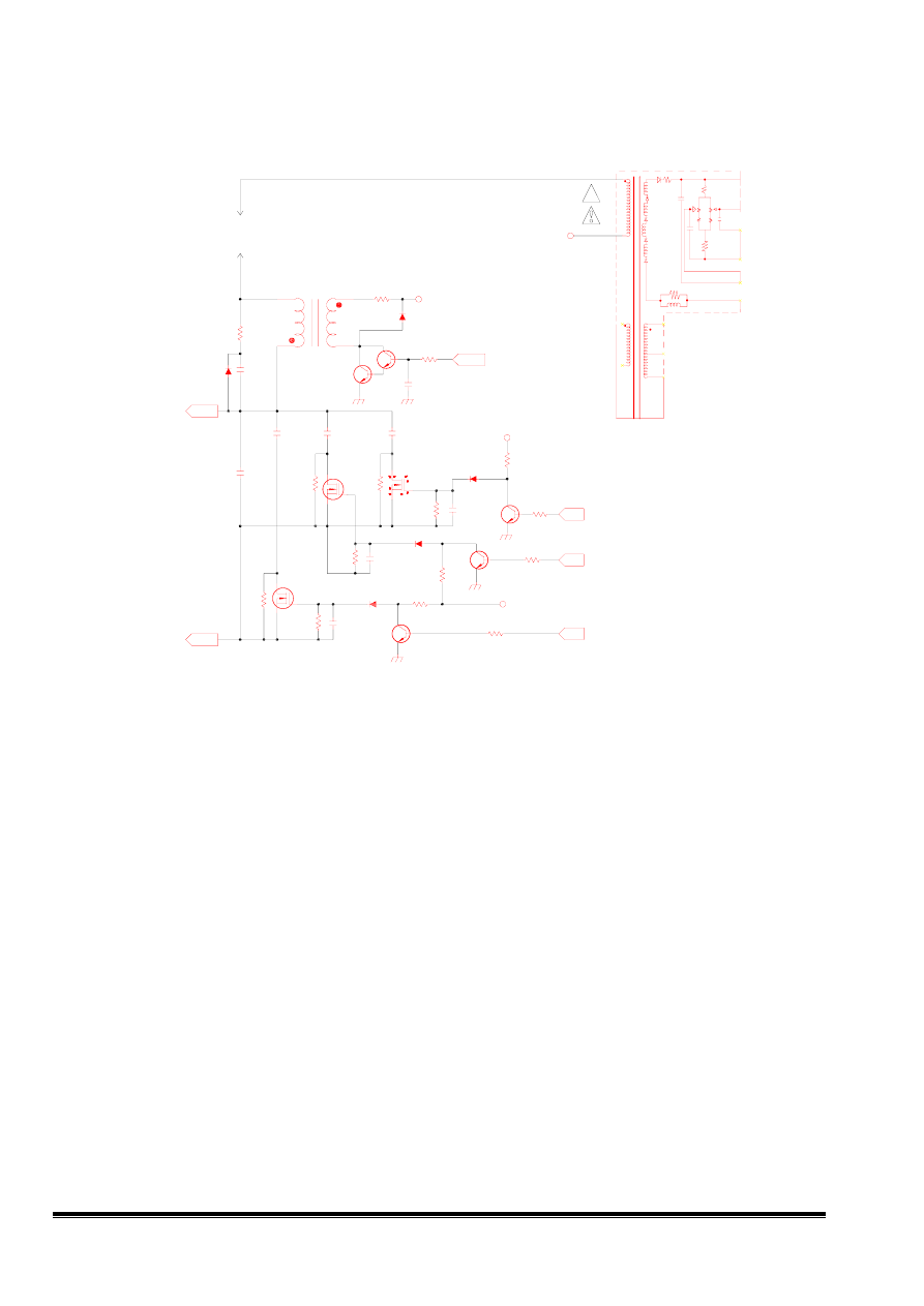
6. BDRV and step-up CKT
6.1 The "BDRV" signal from TDA4856 pin6 is a square waveform. It is inverted and amplified by
Q201, Q311 and Q312 constitute a buffer stage.
6.2 Q325, L301, D318, C323 is step-up circuit B+ = 45 * ( T
on
+ T
off
) / T
off
.
R370
C322
L301
Q312
C323
Q311
C334
Q325
D318
R371
R333
47
100V
(OPEN)
(PE)
19.40195.001
900UH
A733
250V
4.7U
(EL)
H945
(D)
1KV
1000P
IRF630
UG4D
10K
1W
10
PWM
+45V
B+
+14V
A
Fig 6 BDRV & Step-up circuit
5
Confidential

V772 CRT Monitor Service Guide
Circuit Operation Theory
7. HV Shutdown Circuit
The IC201 pin2 (XRAY) provides a voltage detector with a threshold. If the voltage at pin XRAY
exceeds this threshold (6.25v typical) the pins HDRV, BDRV, VOUT1 and VOUT2 are floating.
When anode voltage increases, the voltage at FBT (pin3) increases, the voltage at IC201 pin2 increases.
The shutdown voltage is about 28KV.
C204
R216
R217
R218
IC201
50V
2.2U
(EL)
15.8K
(1%)
100K
(1%)
22.1K
(1%)
TDA4856
+48V
TP3
TP2
+
GND
HPLL2
HSMOD
FOCUS
SGND
VSMOD
ASCOR
SDA
SCL
HUNLOCK
VCC
i.c.
BDRV
HFLB
32
31
30
29
28
27
26
25
24
23
22
21
20
19
18
17
CLBL
HSYNC
VSYNC
VOUT1
VOUT2
EWDRV
VAGC
VCAP
VREF
HPLL1
HBUF
HREF
HCAP
HDRV
BIN
BSENS
BOP
XRAY
16
15
14
13
12
11
10
9
8
7
6
5
4
3
2
1
Fig 7 HV- shutdown CKT
8.Horizontal linearity CKT
V772 Cs control truth table
Frequency range SC0 SC1 SC2 Cs Capacitor
Fh< 36K
0 0 0 C310+C311+C312+C313
36K<Fh<40K 0 0 1 C310+C311+C312
40K<Fh<51K 1 0 1 C310+C312
51K<Fh<62K 1 0 1 C310+C312
62K<Fh<72K 1 1 1 C310
6
Confidential
V772 CRT Monitor Service Guide
Circuit Operation Theory
Q322
D322
C330
Q324
R322
Q303
R320
Q304
R338
R319
Q308
D310
Q307
C321
Q305
C311
C313
C310
C312
D311
D309
Q309
C316
C315
R313
R317
C317
R312
R311
R316
R324
R309
R326
R325
R321
L304
R315
T301
D312
H945
1N4148
(OPEN)
50V
(D)
C2235
2W
10
H945
1/4W
100K
H945
1/4W
100K
10K
IRF630
FR155
IRF640
1KV
560P
H945
250V
1.0U
(MPP)
(MPP)
250V
0.15U
400V
0.3U
(MPP)
250V
0.33
(MPP)
FR155
FR155
IRF630
0.047U
50V
(D)
(D)
50V
0.047U
47K
47K
0.047U
50V
(D)
4.7K
47K
4.7K
47K
2W
220
4.7K
47K
1/4W
100K
19.50051.051
10UH
47K
19.70066.001
RGP10J
SC0
SC2
SC1
DYH+
B+
DYH-
CS-2
H-LIN
+14V
+14V
+6.5V
CS-1
*
A
A
A
A
B
B
D
5
4
3
2
6
5
(RED)
(WHT)
9
4
3
8
16
12
15
2
1
Fig 8 Linear circuit
7
Confidential
V772 CRT Monitor Service Guide
Circuit Operation Theory
9. ABL CIRCUIT
When the beam current is over the limited current, the ABL circuit will pull down the
voltage of the video preamp (pin 10) to reduce the gain of video amplifier.
R308
R314
R310
D307
D306
C324
T301
10K
1/2W
6.8K
1.5K
1N4148
1N4148
100V
1500P
(PE)
19.70066.001
ABL
ABLADJ
6
5
(RED)
(WHT)
9
4
3
8
16
12
15
2
1
Fig 9 ABL circuit
8
Confidential
V772 CRT Monitor Service Guide
Circuit Operation Theory
10. TILT CKT
We can rotate raster clockwise or counterclockwise by changing the direction of the current flow
through the tilt coil.
When the voltage of MP202 (pin3) is larger than 8V, the current flows from Q205 to Tilt coil, other
wise, the current flows from tilt coil to Q206
C228
Q206
MP202
R246
R247
R244
R249
Q204
C225
Q205
Q210
R243
Q207
R245
50V
2.2U
(EL)
A733
TILT-COIL
3P
10K
2.2K
2.2K
1/4W
(OPEN)
H945
50V
2.2U
(EL)
H945
A733
(OPEN)
H945
10K
TILT
+6.5V
+5V
+14V
+14V
+
3
2
1
+
Fig 10 TILT circuit
9
Confidential
V772 CRT Monitor Service Guide
Circuit Operation Theory
11. Vertical Output Circuit
This vertical driver IC circuit is a half bridge configuration
The signals from TDA4856 OSC IC to TDA4863AJ
TR201
C219
C218
C214
C213
R229
R227
R228
R251
R224
R226
R250
R252
R275
R274
R225
ZD202
IC202
C216
C215
C217
D202
R253
C220
100
(PE)
100V
5600P
(PE)
100V
5600P
35V
100U
(EL)
(105C)
25V
1000U
(EL)
1K
(FS)
1/2W
0.22
1K
1.8K
1/4W
5.6
270
1.8K
1/4W
180
27K
33K
1/2W
1
20V
TDA4863AJ
(PE)
100V
0.1U
16V
470U
(EL)
16V
470U
(EL)
1N4003
1/4W
180
(PE)
100V
0.1U
V2
V+
DYV+
DYV-
-8.5V
+14V
V1
+
+
VP3
INP
INN
V-OUT
GND
VP2
VP1
7
6
5
4
3
2
1
+
+
Fig11 Vertical output circuit
10
Confidential
V772 CRT Monitor Service Guide
Circuit Operation Theory
Switching Power Supply Operation Theory
1. General Specification
Input Voltage: 90~264VAC (FULL RANGE)
Input Frequency: 47~63Hz
Output Requirement:
Dc Output
+6V
+13V
+78V
+45V
-10V
2. Block Diagram
DEGAUSS
CIRCUIT
RFI
FILTER
RECTIFIER
&
FILTER
SWITCHING
ELEMENT
FEEDBACK
CONTROL
CIRCUIT
ISOLATION
TRANSFOR
-MER
POWER
SAVING
CONTROL
OUTPUT
RECTIFIER
AND
FILTER
OUTPUT
AC
INPUT
3. Circuit Operation Theorem
3.1 RFI FILTER
250V
2200P
(Y)
C602
3
4
1
2
L602
250V
2200P
(Y)
C603
L604
L603
250V
0.47U
(X)
C601
N
FG
L
R601
This circuit designed to inhibit electric and magnetic interference for meet FCC, VDE, VCCI standard
requirements.
11
Confidential
V772 CRT Monitor Service Guide
Circuit Operation Theory
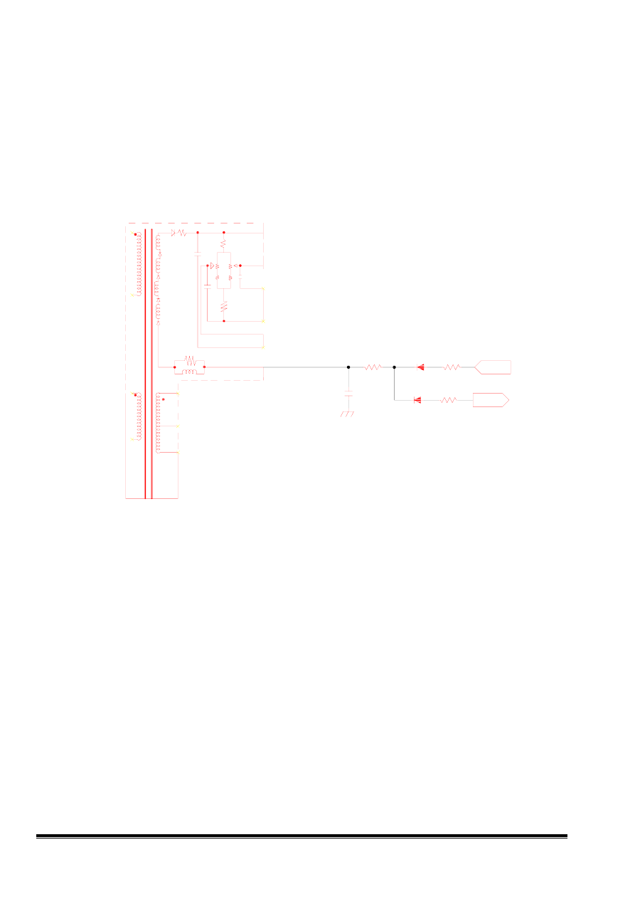
3.2 Rectifier and filter
2
4
3
1
~
~
-
+
D602~D605
20D6 * 4
+
400V
220U
(EL)
C612
L
N
DC OUTPUT
AC INPUT
When power switch is turn on, the AC voltage is Rectifier and filter by D603~D606, C612. The DC
output voltage will be 1.4*(ac input)
3.3 switching Element and isolation transformer
B61
C53
C51
C50
*
D613
ZD601
FR702
FR704
FR701
T601
Q602
L608
L606
L607
C613
C624
C614
D610
D608
D614
R607
R608
R611
R604
R619
C608
(OPEN)
(OPEN)
(SHORT)
(SHORT)
(SHORT)
FS14SM-12
(BEAD)
(BEAD)
(BEAD)
(D)
1KV
0.01U
(D)
1KV
220P
(OPEN)
EGP30B
UF4007
RGP10D
UF4007
2W
0.15
20K
1K
2W
82K
2W
470
25V
47U
(EL)
13
12
11
10
8
1
6
16
15
18
9
In a flyback converter operated in the discontinuous mode, the energy stored in the flyback
transformer(actually an inductor) must be zero at the beginning and end of each switching
period.
During the "ON" time, energy taken from the input is stored in the transformer when
12
Confidential
V772 CRT Monitor Service Guide
Circuit Operation Theory
the switching transistor turn-off, this stored energy is all delivered to the output.
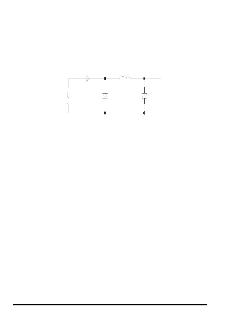
3.4 Output Rectifier and filter
The structure of each output is illustrated as below
T601
+
C1
+
C2
D1
L1
since the transformer T601 acts as a storing energy inductance, diode D1 and capacitor C1 are to
produce a dc output and additional L1, C2 to suppress high-frequency switching spikes.
13
Confidential
V772 CRT Monitor Service Guide
Circuit Operation Theory
3.5 Control circuit
*
*
4
1
VCC
OUT
ISSEN
GND
FB
COMP
R/C
VREF
7
6
4
3
5
2
1
8
G
K
A
+
+
IC601
IC603
ZD602
ZD603
M603
M604
C619
C620
C618
C625
D611
D612
R620
R613
R607
R611
R615
R614
R612
R738
R616
R622
C627
C617
C615
C616
UC3842
MCR100-3
24V
5.1V
(D)
50V
0.022U
(D)
50V
820P
(D)
50V
0.01U
(OPEN)
1N4148
1N4148
1N4004
10K
36K
2W
0.15
1K
51K
100K
47
1/2W
82
10K
510
50V
10U
(EL)
50V
4.7U
(EL)
50V
2200P
(PE)
100V
0.01U
(PE)
+6.5VA
The current mode control IC UC3842 is used in the switching power supply which function of each
pin
described as follows.
pin 1 : Error amplifier output
pin 5 : Ground
pin 2 : Error amplifier reverse input
pin 6 : Output
pin 3 : Current sense
pin 7 : VCC
pin 4 : OSC sawtooth
pin 8 : Reference Voltage:5V
14
Confidential
V772 CRT Monitor Service Guide
Circuit Operation Theory
When power is initially applied to the circuit, capacitor C626 charges through R624, R623, ZD601.
When the voltage across C607 reaches a level of 16V, IC601 is turn-on the +5Vdc will be
set up at pin8 then R613, C615 generate a fixed frequency sawtooth wave to pin4, at this time
MOSFET will be driver by pin6 with square wave the pulse width of square wave is decided by
pin2, pin3 is current feedback control, It will to sense MOSFET current. The D613, D612, R614,
C617 are soft start components to avoid the duty too large when power starts up.
3.6 Feedback circuit
This power supply is a primary feedback circuit. It used IC601 for voltage regulation
, The output voltage differential signal will be detected and sensed to the pin2 of UC3842 for
comparison then the duty cycle of MOSFET will be decided to control the output voltage.
*
*
*
IC601
ZD602
C619
C620
C618
D612
D613
VR601
R611
R615
R617
R614
C609
R616
C617
R618
UC3842B
24V
(D)
50V
0.022U
(D)
50V
820P
(D)
50V
0.01U
(D)
50V
(OPEN)
1N4148
1N4148
2K
2W
0.15
1K
560K
9.09K
100K
50V
0.22U
(EL)
57.6K
50V
10U
(EL)
(OPEN)
VCC
OUT
ISSEN
GND
FB
COMP
R/C
VREF
7
6
4
3
5
2
1
8
+
1
+
15
Confidential
V772 CRT Monitor Service Guide
Circuit Operation Theory
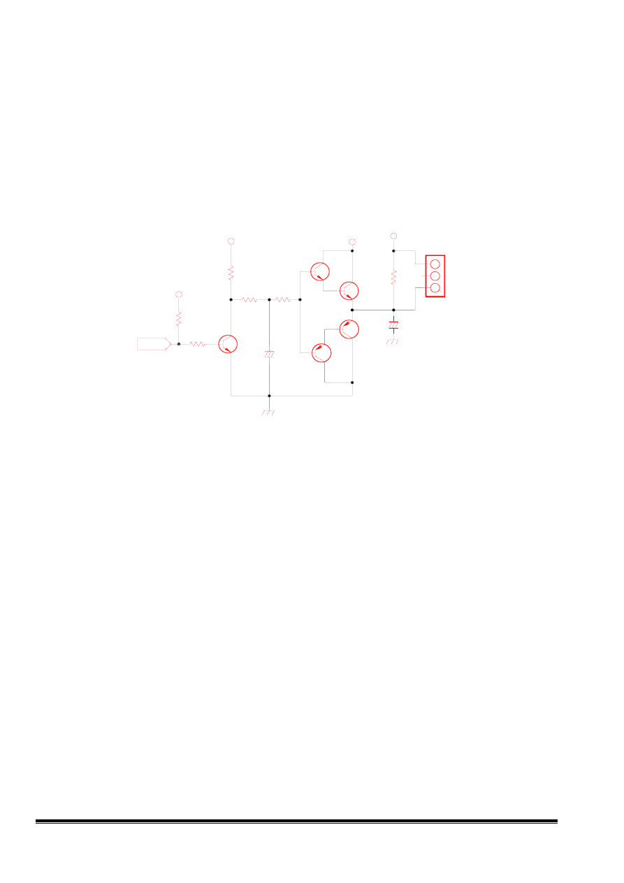
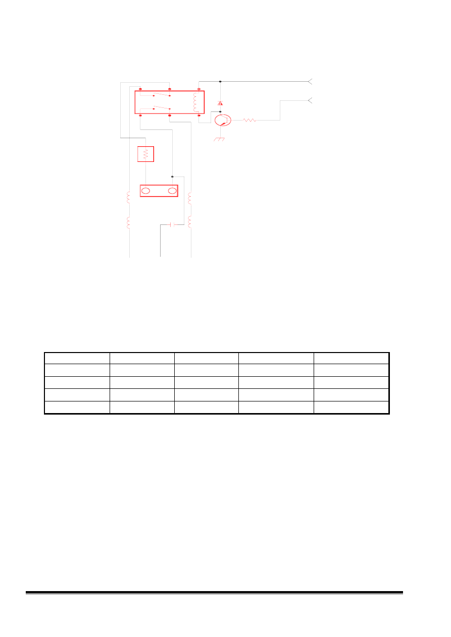
3.7 DEGAUSS CIRCUIT
RL601
C604
Q740
R741
D740
L604
L603
TR602
M602
L610
L611
250V
(OPEN)
(Y)
H945
2.2K
1N4148
180UH
180UH
2R9M
2P
3T
3T
DEGAUSS
+12V
B53
4
3
1
2
5
6
2
1
This circuit has the function of auto degaussing and manual degaussing. When power supply is
switched ON it is auto degaussing stage. When user make the selection of the manual degaussing
function in OSD, the degaussing current will flow through coil to degauss the screen of monitor.
TR602 is a PTCR to control degaussing coil current
3.8 power saving control
Mode H-sync
V-sync
LED
Power
Rating
Normal Normal Normal Green
100﹪
Stand-by None
Normal Amber
≦ 5W
Suspend Normal None
Amber
≦ 5W
Off None
None
Amber
≦ 5W
When both of the H-sync and V-sync are none, the power supply +14v output will be cut-off.
The power input will be under 5W.
When the H-sync or V-sync is none, the power supply +14v output will be cut-off. The power input
will be under 5W.
16
Confidential
V772 CRT Monitor Service Guide
Circuit Operation Theory
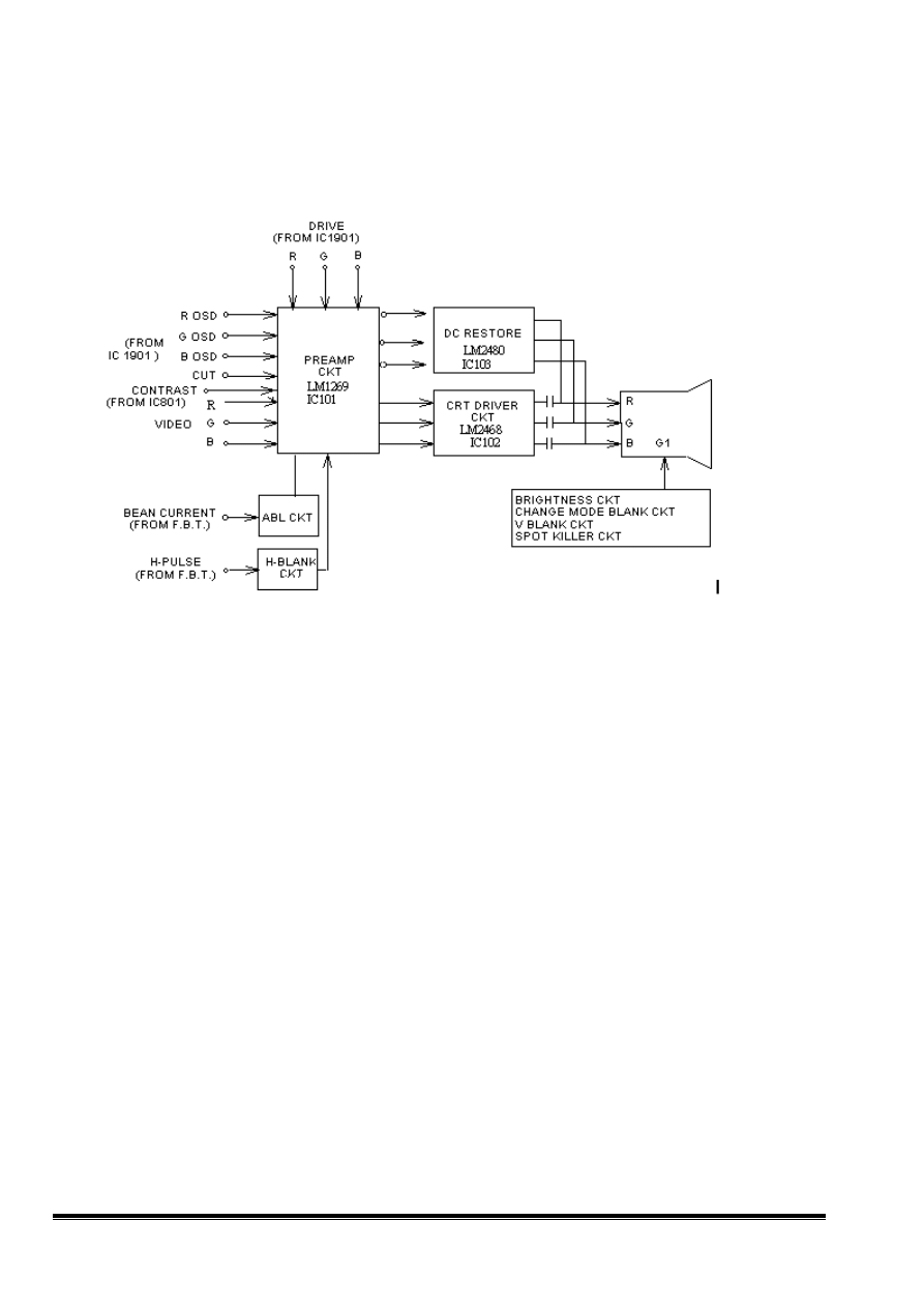
30. Video CKT
V772 VIDEO C.K.T. BLOCK DIAGRAM:
31. OSD Preamp CKT:
(a) AS shown in the block diagram:
The R/G/B signals will generate an enough amplitude of Vpp to show up on the
CRT screen after the amplification of two amplifiers. The first one, preamp CKT,
process the signal and mix up the OSD, and the second one does the power
amplification.
(b) OSD preamp IC101, LM1269, will output the R.G.B signals separated. The R.G, B
driver will control the gain of these three guns individually to approach the white
balance of CRT.
(c) The signal H-Blank is to let the output of LM1269 down to 0.2V while non-display
duration. Then the CRT driver CKT will generate a level higher than Black Level. (i.e.
SYNC TIP), therefore the video signal will be blanked in order to prevent the fold over
to occure while adjusting H-phase. Besides, the SYNC TIP is used for
the DC Restoration of cascode CKT.
(d) LM1269 is equipped with OSD mixer, when signal CUT is Low, the output of
LM1269 is video signal when signal CUT goes high, the output will be OSD signal.
17
Confidential

V772 CRT Monitor Service Guide
Circuit Operation Theory
32. CRT DRIVER CKT:
Output stage adopts CRT driver LM2468 to amplify the signal which has been
recessed by LM1269 to a enough amplitude of Vpp, then display on the CRT. The IC
contains three high input impedance, wide band amplifiers which directly drive the
RGB cathodes of a CRT. The gain of each channel is internally set at -15 and can
drive CRT capacitive loads as well as resistive loads presented by other application
limited only by the package’s power dissipation.
33. DC Restore CKT:
(a) The video signal amplified by the output stage is coupled to CRT by way of AC
coupling. So DC restoration CKT is needed to do the white balance adjustment.
(b) This DC restoration circuit adopts SYNC TIP CLAMP, in the duration of
SYNC TIP the capacitor charges, and the capacitor discharge in the other time.
The Black Level is kept to the level of DC restoration set by UC.
34. ABL CKT: (Auto Brightness Limit)
ABL is a protection circuit. When the anode current goes higher than the setting
value of ABL circuit. ABL will pull down the voltage of contrast to limit the anode
current. This is helpful to protect CRT.
35. H-BLANK CKT:
Affair the collect pulse comes from FBT being shaped and inverted, it will be sent
to preamp CKT and used as the H-Blank.
36. Brightness, V-blank, change mode blank, spot killer CKT:
(a) About the cut off voltage , while the voltage, cathode to G1 , over the cut off ,
voltage, the picture will disappear, If cut off voltage of the CRT is
set at 110V and the black level of cathode is 60v, the picture won’t show,
the signals higher the black level once the G1 voltage is lower than-50v.
(b) As described above, we may using the voltage control G1 as the brightness
control. Generally the G1 control range is about 10~15V if the raster
brightness is form 0 to 0.8 ft-L.
(c) Similarly, we may overlap a negative pulse of vertical duration on the G1
voltage to prevent the vertical retrace line from showing on the picture , This
is to keep the voltage cathode to G1 over the cut off voltage during the
period of vertical retrace.
18
Confidential

V772 CRT Monitor Service Guide
Circuit Operation Theory
(d) In order to avoid the picture occur transiently while change mode, pull
down the G1 voltage and let the voltage cathode to G1 over CUT OFF voltage.
This will make the picture blanking.
(e) While monitor turned off , the discharge speed of high voltage circuit is slow
since there is no deflection scan act on the electronic beam, a spot which will
destroy the phosphor of CRT. So the SPOT KILLER circuit will generate a
negative voltage higher than CUT OFF to the G1 to beam this is to protect
the CRT.
19
Confidential
V772 CRT Monitor Service Guide
Circuit Operation Theory
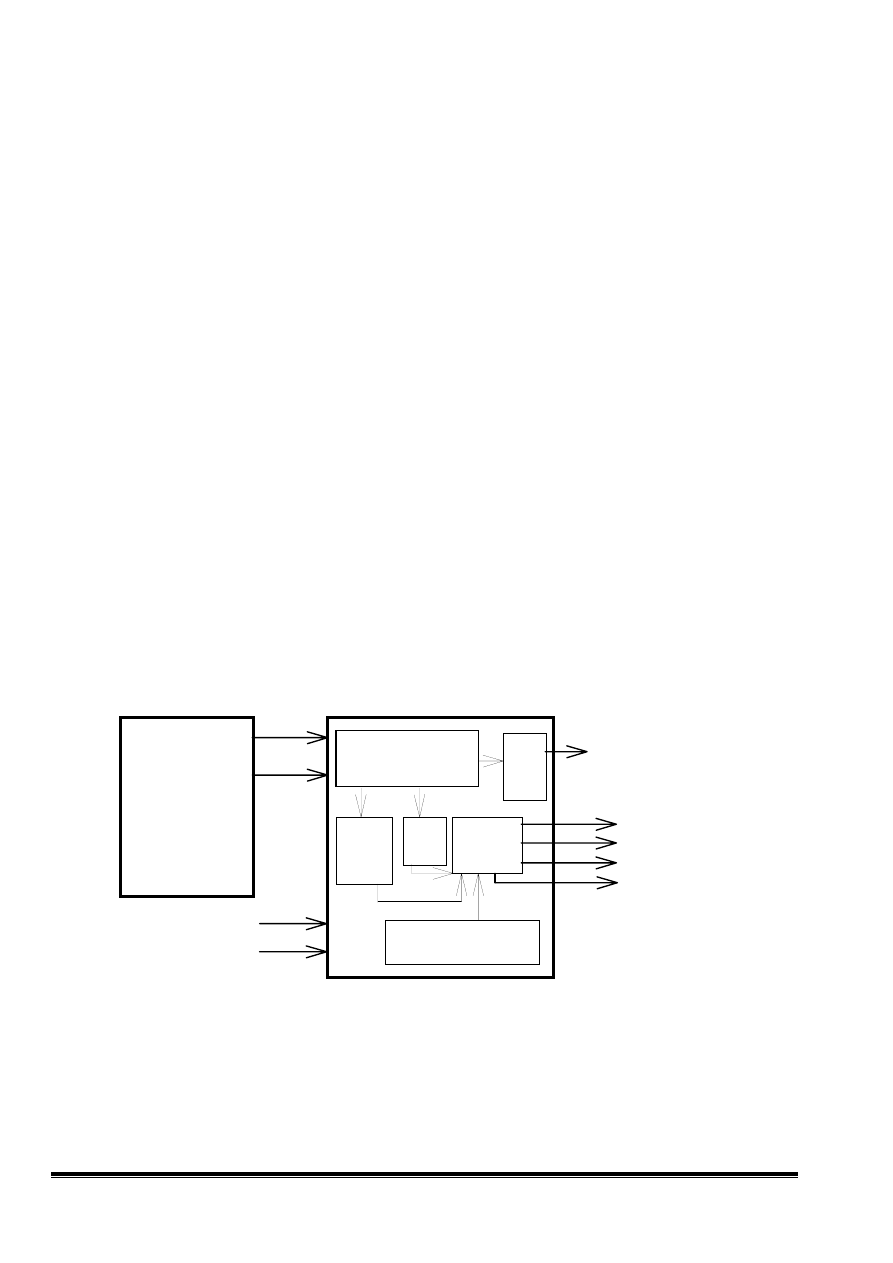
ACER V772 MICROCONTROLLER CIRCUIT OPERATION THEORY
1. Introduction:
This model, V772, will support powerful OSD function to help end user fine adjustment. The
Microcontroller circuit of the V772 can determine what mode it is by detecting the frequency of
horizontal and vertical synchronous and the polarity of horizontal synchronous, and provide DC
voltages to control the picture and save the adjusted value into the EEPROM by using the OSD,
"On Screen Display control", that means the user can get any information of the picture display or
adjust it and save the status values into the EEPROM by choosing and pressing the proper key
according to the indication of the OSD. In addition, user can press i-key to do auto-calibration.
2.
Block diagram :
The major parts of V772 Microcontroller circuit are MCU, EEPROM, OSD IC, and Auto
Calibration Module. The circuit block diagram is shown as below.
MCU
(MTV112)
Hsync
Vsync
H-polarity
Preset mode data,
User saved mode data.
Searching for
the same saved
mode timing
with the input
signals and
get the data.
Detecting the
input signals
of H,Vsync &
H-polarity.
Control Panel
5 keys input
i-key
Left,Right,Enter,Exit
Checking if the
valid key be pressed
and do key function.
Degaussing
Blanking
SC0 - SC2
PWM
output
OSD IC
Display OSD
and output
PWM to video
circuit
To deflection
circuit
(UART) External
adjustment
function
PC
RS232
auto alignment
program
EEPROM
Reset circuit
12MHz Crystal
circuit
Auto
Calibration
Module
DCLK
DATA
HBNK
VBNK
RGB
Signal
AP3113
20
Confidential

V772 CRT Monitor Service Guide
Circuit Operation Theory
3.MCU and the peripheral circuit operation theory:
3-1.MCU function:
The MCU is MTV112, it is an 87C51 with PWM output controlled microcontroller, after
power on, the reset circuit output a "High" to "Low" signal (>40mS) and the 12MHz crystal
oscillated circuit working, the MCU begin to manages the following functions,
(1) To detect mode and output proper SC0, SC1 and SC2 to deflection circuit.
(2) To check if there is the same saved mode in the EEPROM and get the data to transfer into
DC voltages by PWM output and RC filter circuits to control the picture, color, contrast
and brightness.
(3) To check if there is the valid key be pressed and do the key function.
(4) To memorize mode timings and any adjustable parameters of the picture into EEPROM.
(5) To output data to OSD IC for making an "on screen display control" menu.
(6) The inner registers and PWM output of MCU can be controlled by the external PC
alignment program.
(7) To calibrate the size, position, and geometry of the picture by pressing i-key. It will be
placed right size and position.
3-2.How to detect mode timing:
Only when the mode timing input is stable, we can adjust the picture and check the
horizontal and vertical sync frequency by the OSD menu, and the mode timing input mean the
horizontal sync signal and the vertical sync signal.
(1) The vertical sync frequency measurement:
We use the base timer, it can generate a count during a fixed time, this fixed time is
12/12MHz and we call it "Time base", so when the first vertical sync generated, we enable
the base timer, and the next vertical sync generated, we disable the base timer, and we only
need to calculate how many counts are during a vertical sync period. The formula is
Vertical sync frequency
= FV
= 1 / Vertical sync period
= 1 / [Counts * (Time base)]
==> Vertical sync frequency = 1000000 / Counts
(2) The horizontal sync frequency measurement:
We use the event counter for calculating how many counts are during a long fixed time,
because the vertical sync period is longer than the horizontal sync period, we can enable the
event counter when the first vertical sync generated and disable the event counter when the
next vertical sync generated, this time, we can get the horizontal sync counts during a vertical
sync period.
The formula is Horizontal sync frequency
= FH
= Horizontal sync counts / Vertical sync period
==> Horizontal sync frequency
= Horizontal sync Counts / Vertical sync period
21
Confidential
V772 CRT Monitor Service Guide
Circuit Operation Theory
3-3.What are the valid key functions for user:
There are four keys on V772 control panel. They are "Left," "Right," "Enter," and "Exit."
There are used for OSD controlling. "Enter" for entering sub-menu of main menu, "Exit"
for escaping to main menu from sub-menu or leaving OSD menu, and "Left," "Right" for
adjusting the bar value.
Except the OSD basic key functions, the user can only press "Right" for brightness
adjustment, or "Left" for contrast adjustment.
3-4.How to memorize the timing and adjusted data:
The EEPROM of V772 is 24C08, it has 1024 bytes memory size and communicates with
MCU by two wires of I2C bus, one wire is "SCL," the other is "SDA".
The MCU send clock and data to EEPROM to do "Write" function and send clock and
receive data from EEPROM to do "Read" function by these two wires.
We define three parts of storage area. One is for the storage of the factory preset data,
another is for saving user adjusted data, the other is for common settings area where stored
the data of the OSD color temperature settings, contrast and brightness value.
3-5.How to display the OSD menu:
The OSD IC of V772 is AP3122 which is developed by vender, it receives the data of the
OSD fonts and attribute what we want to display on the screen from the MCU by 2 wires of
communication, and exports OSD window data and PWM volume to the VIDEO circuit, the
block diagram is shown as below,
SDA
SCL
MCU(MTV112)
Output to
the VIDEO circu
OSD IC (AP3114)
Shift receiving
register and decoder.
PWM
output
Control
register
s
RAM Fonts
generator
VCO circuit
ROUT
GOUT
BOUT
FBKGC
VSYNC
HSYNC
(1)Send data to
RAM for OSD
fonts or
attribute.
(2)Send data to
Control
registers
for PWM ouput
(H-BLANK,HBNK)
or OSD window
3-6.How to execute the auto alignment function:
The MCU MTV112 supports the UART function, it has 2 I/O serious ports, one is the
receiver, the other is the transmitter, they are connected with an interface to PC and PC can
execute alignment program by RS232 communication to send the formatted data to the MCU
for adjusting any adjustable parameters of the picture and saving the adjusted values into
22
Confidential

V772 CRT Monitor Service Guide
Circuit Operation Theory
EEPROM. By this way, we can get the products with the same quality and reduce the
manufacturing time.
23
Confidential
Document Outline
Wyszukiwarka
Podobne podstrony:
75 WHEEL ALIGNMENT THEORY OPERATION
Actuators and Sensors Stepper Motors Stepper Motor Operation and Theory
Operation of an IGBT in a self clamped inductive switching circuit (SCIS) for automotive ignition p
Theory of Operation
wheel alignment theory operation
theoryof operation
Operation of an IGBT in a self clamped inductive switching circuit (SCIS) for automotive ignition p
97 Review of Circuit Theory
Xenon Motherboard theory of operations
theory operation
The uA741 Operational Amplifier[1]
operatory i funkcje matematyczne
(ebook PDF)Shannon A Mathematical Theory Of Communication RXK2WIS2ZEJTDZ75G7VI3OC6ZO2P57GO3E27QNQ
operator maszyn lesnych 833[02] o1 03 n
Goertzel Theory
więcej podobnych podstron