
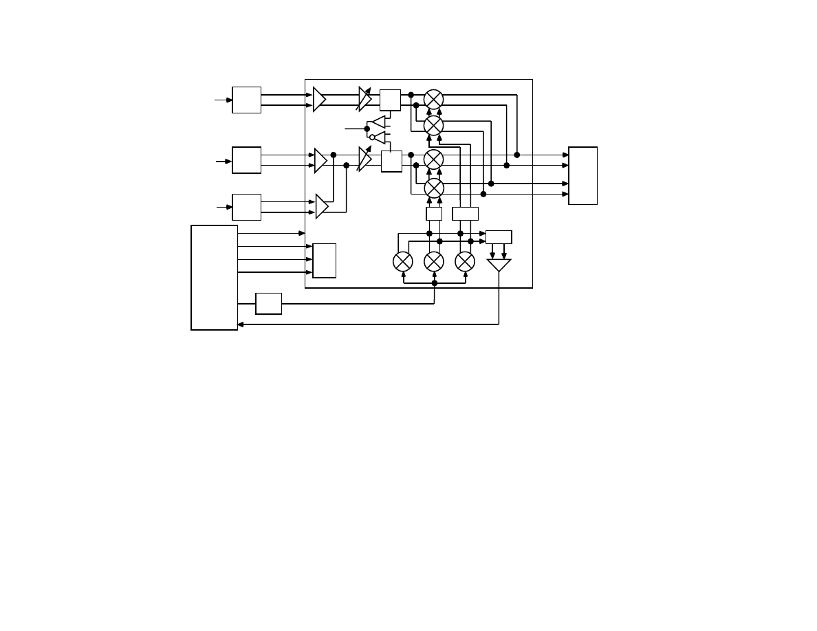
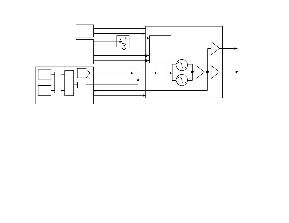
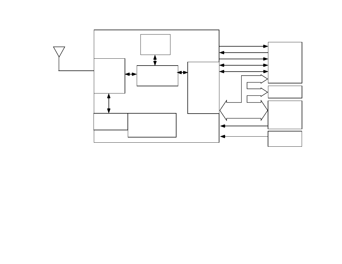
A835:
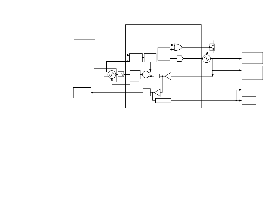
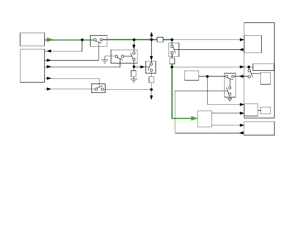
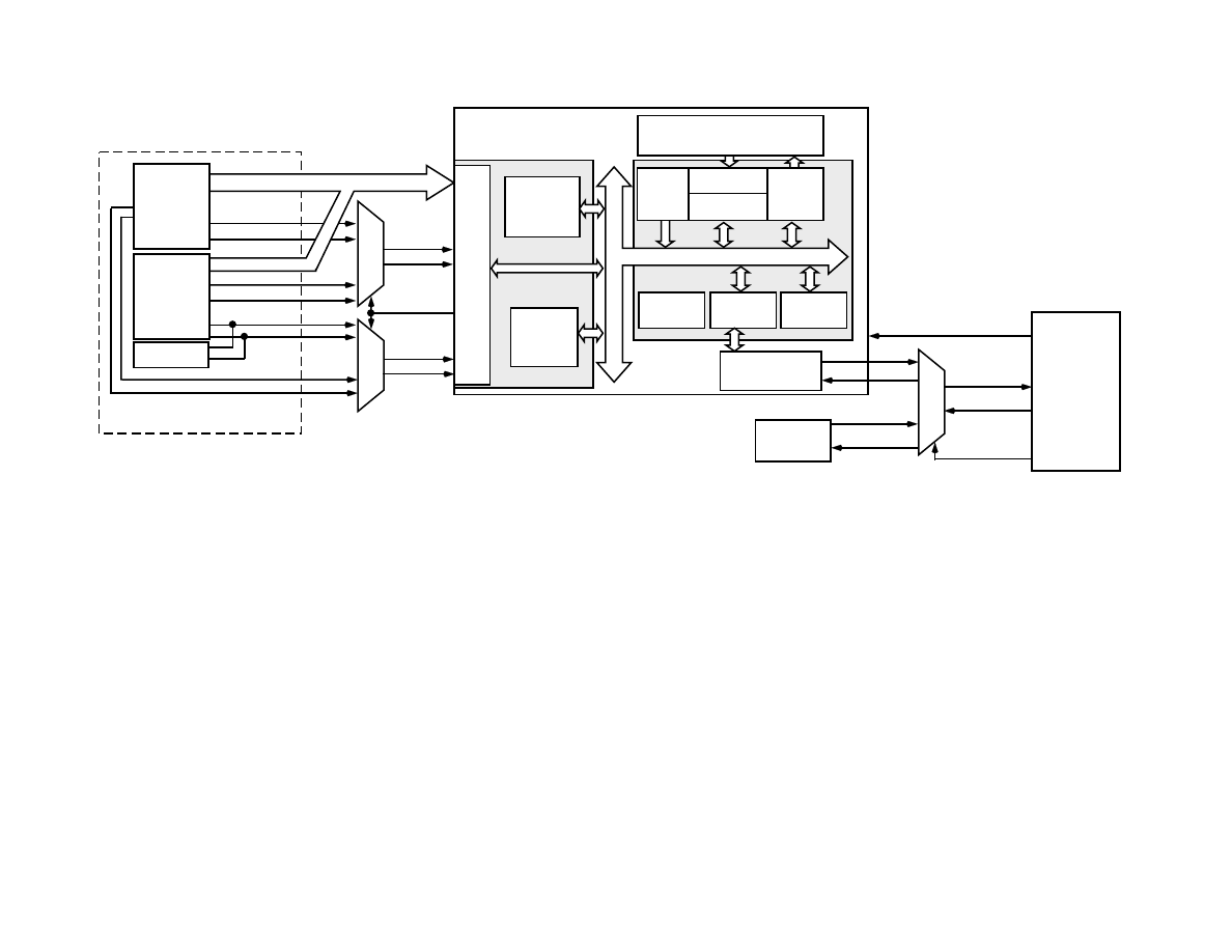
Antenna Circuit
Description
All cellular receive bands are fed into either the internal antenna or external antenna. M001 is a mechanical switch which has the internal antenna path connected when a
no insertion condition exists. The RF path will switch to external antenna upon insertion of a male SMA connector to M001. The internal antenna path is fed to the
FEM(Front End Module) through antenna matching components. The FEM provides band selection and filtering between the EGSM, DCS, PCS and WCDMA receive
and transmit bands to a single antenna port. GSM band selection is done by control lines N_BAND_1 and N_BAND_0_G. Mode selection is done by control lines
HL_TX_EN, RX_EN_LIFE, N_GSM_EXC_EN, and GSM_EXC_EN. The diplexing arrangement permits reception of WCDMA signals in any FEM switch position.
This allows the phone, while in a GSM call in any band, to detect signals from a WCDMA base station. The decision may then be made to hand over to the WCDMA
system. Similarly, EGSM base station signals can be detected while the phone is in a WCDMA call to permit a handover decision from WCDMA to EGSM (This is not
possible for base station signals in the DCS and PCS bands.).
Signals received at the antenna between 2110 - 2170MHz will see the RF switch as an open circuit at any position. Consequently WCDMA Rx signals will go through
FL002 to the WCDMA receiver. FL002 should have a maximum insertion loss of ~0.5dB. Outside of the WCDMA Rx band, FL002 behaves as an open circuit, prevent-
ing out-of-band signals from reaching the WCDMA receiver.
GSM, DCS, and PCS receive signals from the antenna port through the FEM should have a maximum insertion loss of -4.4dB. The FEM EGSM transmit path should
have a maximum insertion loss of -2.5dB. The FEM DCS transmit path should have a maximum insertion loss of -3.1dB. The FEM PCS transmit path should have a
maximum insertion loss of -3.7dB.
Q902 is a dual FET package that’s being used to multiplex function of the N_BAND_0 control signal coming from the Magic LV. With the use of Q902,
N_GSM_EXC_EN will follow N_BAND_0. GSM_EXC_EN will be the inverted level of N_BAND_0. Q906 is another dual FET package that’s used to prevent simulta-
neous GSM and WCDMA transmission conditions. During WCDMA transmission conditions, HL_TX_EN will be in a high state. This will open both FETs in Q906,
thus, disabling any signal functions from control lines NB_EXC_EN and N_BAND_0. Q901 is used to invert the control signal coming from Q906.
Motor
o
la
Conf
ide
n
tia
l Pr
opr
ie
ta
ry
4-
2
Int Antenna
M001
Ant
Match
Ext Antenna
WCDMA
RF SECTION
GSM
RF SECTION
FL001
FEM
CMOS level shifter
Decoder ASIC
WCDMA_TX
WCDMA_RX
FL003
FL002
GSM_RX
DCS_RX
PCS_RX
GSM_TX
DCS_PCS_TX
HL_TX_EN
N_
GSM_
EXC_
EN
N
_BAN
D
_0_G
GSM
_EX
C_EN
HARMONY
LITE
N_BAND_1
RX_EN_LIFE
MAGIC
LV
N_BAND_0
NB_EXC_EN
VRF_TX_2_775V
N_BAND_0
RAINBOW
Q902
Q906
Q901
MAGIC LV
GSM TX VCO
TX RF Coupler
LV_EXC_EN
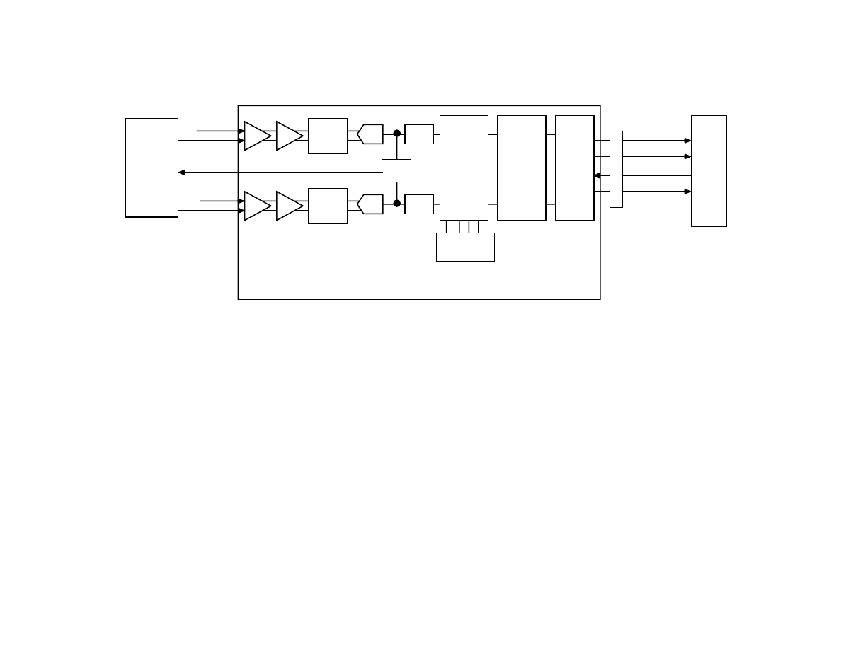
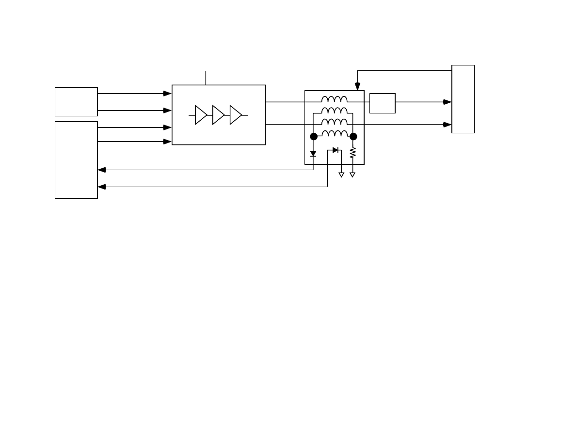
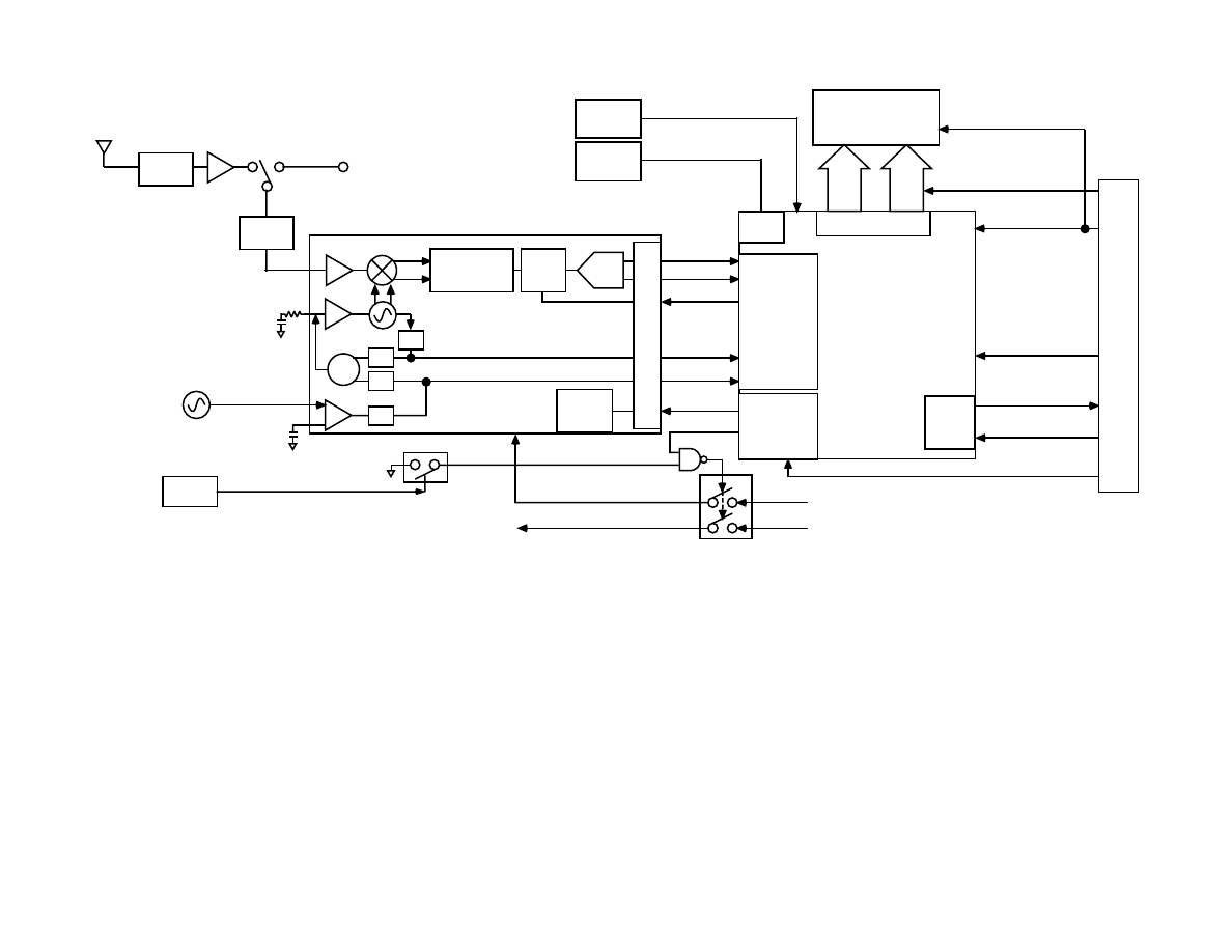
A835:
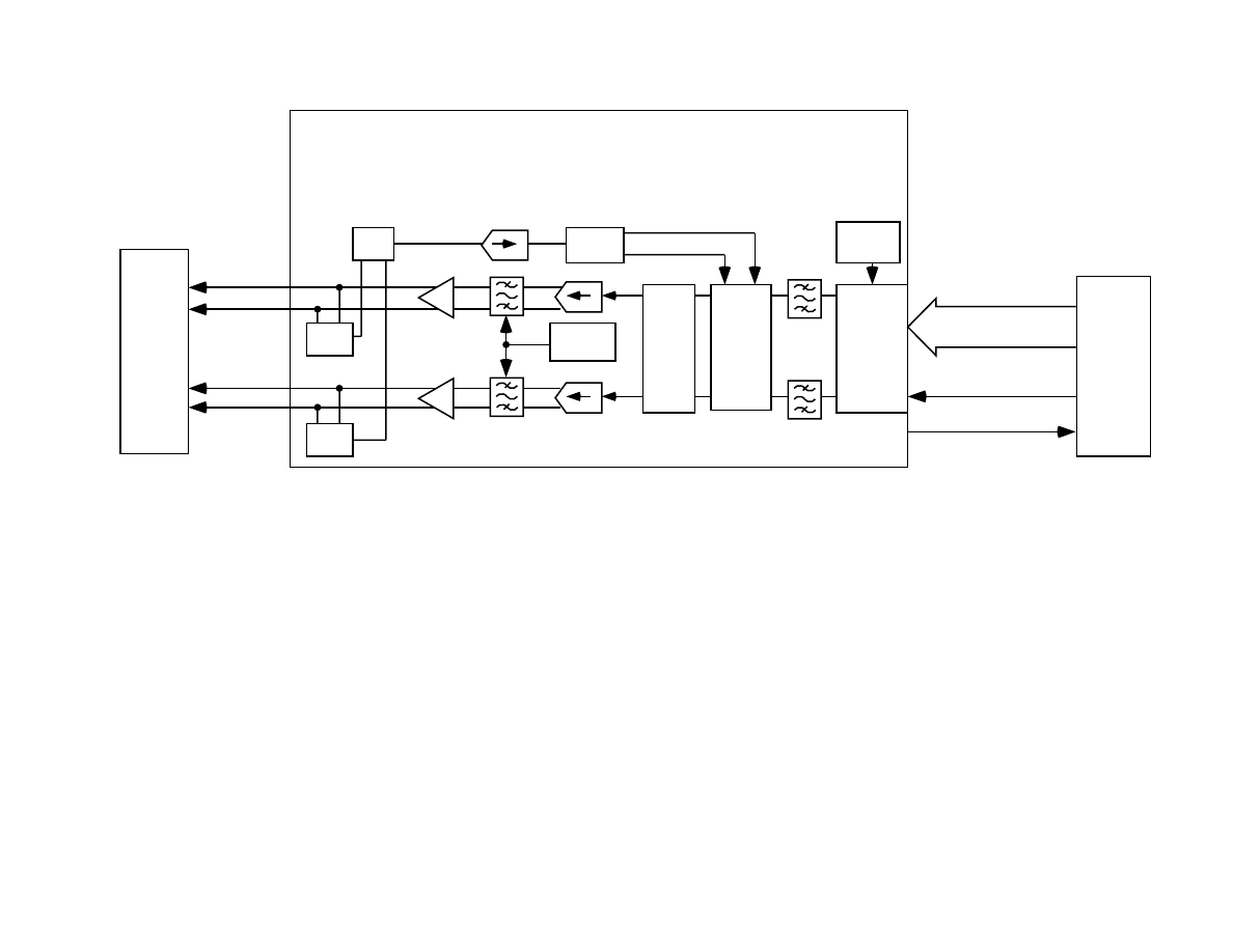
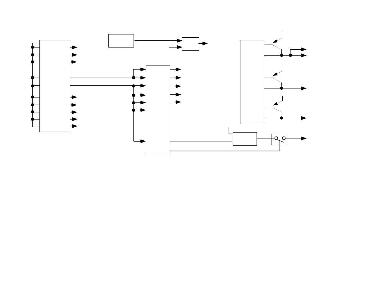
GSM RX Front End
Description
The EGSM, PCS and DCS signals must first pass through baluns before reaching the LIFE IC. Since the LIFE expects differential inputs, the baluns will provide this.
Baluns provide the change from an unbalanced to a balanced line condition. By directly connecting to lines together, a possibility might arise where one line might
ground a signal and impair the operation of a circuit. This situation is solved through the use of an un-balanced to balanced transformer, a balun. Expected nominal loss-
es is ~.5 - 1.0dBm.
The first IC in the EGSM, DCS, and PCS RX line up is U625 (LIFE), which is an LNA, VCO, and down converter mixer. The RX frequency is mixed down to a Very
Low Intermediate Frequency (VLIF) of ~ 100KHz. This design is utilized to improve LO leakage causing RF self-mixing, DC offsets, and noise performance. The LIFE
IC operates from the MAGIC_LV (tracking regulator), MAGIC_RF_V2_475. and MAGIC_SF (isolated supply for the VCO).
LIFE is comprised of four low noise amplifiers (three of which are used) with two quadrature mixer paths for use in receive GSM 900 (925- 960MHz), DCS (1805-
1880MHz), and PCS (1930-1990MHz) frequency bands, all SPI programmable. The RX_VCO signal is fed back to the MAGIC_LV prescaler input. Although the fre-
quency will be dependent of the channel selected, the amplitude signal is ~30dBm.
LIFE contains three fully contained VCOs which operate at ~4GHz. These VCOs are internally divided to provide precise quadrature down conversion for the three
frequency bands. The input signal RX_VTUNE from the RX backend processor (MAGIC_LV) selects the VCO frequency to operate at. The tune range is .5 - 4.5V.
The VCO frequencies for the three technologies are: DCS 3610 - 35759MHz, EGSM 3700 - 3838MHz, and PCS 3859 - 3980MHz.
The AGC is provided by a common amplifier section, which is shared by all four LNAs. The AGC amplifier gain control is controlled by the voltage on the AGC pin,
utilizing the internal 6-bit D/A to set the AGC via the SPI lines (SPIDATA, SPI_CLK, and SPI_CE). LIFE has an internal RF detector at the input of the AGC amplifier.
The detected DC output level will be compared against a reference, which corresponds to the maximum safe input level to the mixer. This reference is SPI selectable so
that the threshold can be set to 0dB, 3dB, 6dB, or 9dB below the level, which results in the mixer malfunction. If the detected level is above the reference then
AGC_FLAG will go high. The MAGIC_LV will receive this signal as an interrupt and will reprogram the AGC until the level drops below the safe mixer input level as
signified by AGC_FLAG returning low.
The output signals I / IX and Q / QX are @ ~100KHz IF value for the Very Low IF. The input pin, RX_EN_LIFE controls the on / off state of the receiver and the PLL
circuits. For input amplitude at the antenna of -50 to -40dBm the expected nominal output should be an AC rms peak-to-peak voltage of ~4.5 - 14mV.
Motor
o
la
Conf
ide
n
tia
l Pr
opr
ie
ta
ry
4-
4
RF
DET
RF
DET
RX_Q+
RX_Q-
RX_I+
RX_I-
GSM_RX
DCS_RX
PCS_RX
T601
T602
SPI
AUX_SPI_CLK
RX_EN_LIFE
LIFE_CE
AUX_SPI_DATA
÷2
÷2 or 4
GSM
PCS
DCS
÷5 or 3
RX_VCO_OUT
RX_VTUNE
LP
Filter
MAGIC
T600
MAGIC
U625
LIFE
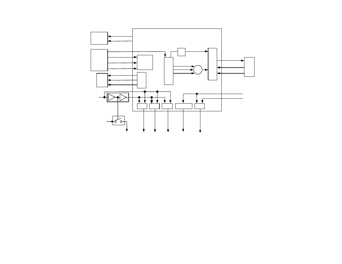
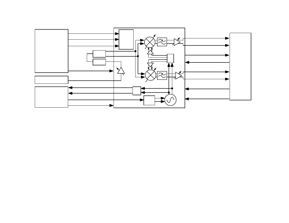
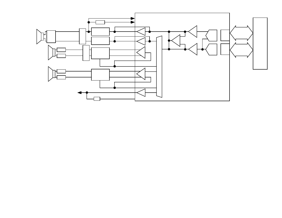
A835:
GSM RX Back End (Magic LV)
Description
The MAGIC_LV (U500) handles the backend processing for the EGSM, DCS and PCS (VLIF: RX_I, RX_I_X, RX_Q, and RX_Q_X) signal lines from LIFE. Simply,
the MAGIC_LV performs an analog to digital conversion of I /Q and sends it to the data to the board processor (RAINBOW) via the SSI (serial synchronous interface).
The MAGIC_LV also has a programmable and phase-able digital IF to improve image rejection.
In MAGICLV, each channel is comprised of a Post Mixer Amplifier (PMA), an integrated passive two pole filter, a gain stage (AMP1) followed by an active programma-
ble 2 pole anti-aliasing filter (mainly required to meet the blocking specs). This is followed by a lowpass sigma-delta ADC with a programmable oversampling clock
OVSCLK (derived from the reference oscillator) equal to 13MHz for 200kHz channel spacing (13bits).
Digital detector circuits are placed on each channel at the output of the sigma delta converters. The outputs of these detectors are compared against a level defined by
DET_LVL. If either of the detected levels exceeds the programmed threshold then the pin DET_FLAG is set high. This indicates that the signal level is excessively high
for the sigma delta modulator. DET_FLAG is read by the processor, which will respond by re-programming one of the AGC settings to a lower gain until DET_FLAG
returns low.
The outputs of the sigma-delta modulators are digitally processed through a noise cancellation circuit, comb and decimation filters. A second programmable digital LO
based on a look up ROM generates digital quadrature oscillators with programmable gain/phase correction (called balanced complex multiplier) to digitally downconvert
the I/Q signals to baseband (digital zero IF) through four quadrature mixers that provide image rejection of adjacent/alternate channels. Gain/ Phase correction at a single
baseband frequency is performed on the Digital Quadrature Oscillator to compensate the analog gain/phase mismatch of the quadrature I and Q paths. After baseband
downconversion and image reduction, the quadrature I and Q signals are further processed by digital filters that perform channel selectivity and out of band noise rejec-
tion.
A serial bus consisting of SDFS and SDRX will transmit the RXI and RXQ data in 2‘s complement format. BDR and BFSR are outputs from MAGIC LV. BFSR is a
framing signal which marks the beginning of an I,Q transfer. BDR is the serial data. The clock used for the serial transfer is BCLKR. When NB_RX_ACQ goes high
MAGIC LV will activate the SSI interface in the digital receiver section. The data transmission over the serial bus will begin at the next normal occurrence of valid I and
Q data, as defined internally to the digital receiver.
Motor
o
la
Conf
ide
n
tia
l Pr
opr
ie
ta
ry
4-
6
PMA
Anti-
Aliasing
filter
Filter
Prgmable
Dig CH Sel
and
Complex
IF Notch
or
Highpass
RX
Serial
Interface
Σ∆
Dig Quad
Osc
Balanced
Complex
Mod
IFA
DET
PMA
Anti-
Aliasing
filter
Filter
Σ∆
IFA
RX_I
RX_I_X
RX_Q
RX_Q_X
DET_FLAG
BFSR
BDR
NB_RX_ACQ
BCLKR
FL500
MAGIC LV
U500
(RX Section)
GSM
RX
Front End
Rainbow
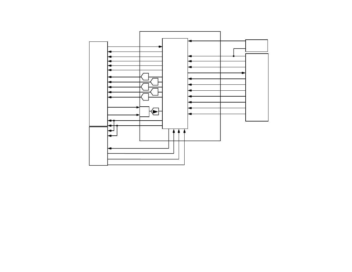
A835:
MAGIC LV Control Functions
Description
The MAGIC LV contains 4 tracking regulators and one superfilter, which will generate the supplies for most of the IC as well as the front end and the main VCO. The
tracking regulators derive their internal power from the REG_REF pins. The reference voltages are filtered and buffered for use on the IC. The buffered voltages should
track the references within +/-1.5%. A raw supply voltage is provided to the tracking regulators which is higher than REG_REF as specified below for each regulator. A
superfilter is needed for the external VCO power supply. This superfilter, cascaded with an external regulator and any filtering in front of the IC, will need to provide
80dB of rejection to a 0.1V step occurring at a 217Hz rate with a risetime of 20us on the raw supply (battery) and a duty cycle of 0.125. The superfilter will use an inter-
nal pass transistor that is capable of driving a 30 mA load with a voltage drop of less than 0.4V relative to SF_SPLY from the SF_OUT pin. An external 1uf cap is
required on SF_OUT. As the superfilter will track SF_SPLY it will need to sense the power on reset and turn off even though its supply may remain active. All supplies
within the IC must be within 5% of their final values after 5msec from the start of POR_LB. The power on reset circuit contained within the crystal reference oscillator is
used to aid this functionality.
The MAGIC_LV has two sets of SPI interfaces; one set is for handling the control interface for the LIFE IC (AUXSPI lines) and ones for interfacing with RAINBOW
(SPI lines). AUX_SPI_DX is the serial data input line. AUX_SPI_CLK is the clock input line, where data shifting occurs at the rising edge of this signal. LIFE_CE is the
clock enable line, active high, for the LIFE IC.
MAGIC_LV will integrate a system of D/As and control logic to generate the power amplifier control ramps. In addition, MAGIC_LV will integrate the op-amps and
comparators which receive the detected output of the power amplifier and create the necessary control voltage to drive the power amplifier control port based on the con-
trol ramps. When TX_KEYM goes high, the ramp controller receives an positive input. This will cause the AOC_DRIVE pin to linearly rise which in turn will cause the
PA output power to rise. The rising PA output power will cause DET_AOC to begin to rise until the DC level on DET_AOC exceeds the DC level on DET_REF by the
intentional offset of the RF detector versus it‘s reference. At this point the “Active Detect” comparator will go low and break the input voltage to the integrator with the
ramp controller. This will cause the PA power to stop rising and hold the present power level as determined by the 8 bit offset value fed to the ramp controller. The PA
control loop is now at a minimal power needed to keep the control system in a closed loop for a controlled ramp up of the power.
The MAGIC uses two SPI driven GPO lines which are used to control the operating bands of the GSM RF circuits. They are N_BAND_0 and N_BAND_1.
When the MAGIC LV is set to battery save mode it will shutdown the receiver analog sectioins (via RX_EN_LIFE), the AOC, the main synthesizer and the superfilter.
Motor
o
la
Conf
ide
n
tia
l Pr
opr
ie
ta
ry
4-
8
V2
V3
V4
V5
R
F_
V3
_1
_8
75
V
R
F_
V4
_1
_8
75
V
R
F_
V
5_
2_
47
5V
Superfilter
S
F_
O
U
T
RF
_V
2_
2_
47
5V
R
A
M
P
C
on
tro
lle
r
AOC_DRIVE
DET_AOC
DET_REF
TX
C
on
tro
lle
r
TX_KEYM
Σ
AOC
Filter
MAGIC_SPICLK
MAGIC_DX
MAGIC_SPI_CS
80 bit
Serial
Reg
Aux
SPI
Cntrl
AUX_SPI_CLK
AUX_SPI_DX
LIFE_CE
LIFE
POG
MAGIC LV
U500
(Control)
N_BAND_1
N_BAND_0
VRF_DIG_1_875V
GSM
TX
RF_TOP
MAGIC_DIG_1_875V
VRF_REF_2_475V
VRF_RX_2_775V
VRF_REF_2_475V
U510
Q510
A835:
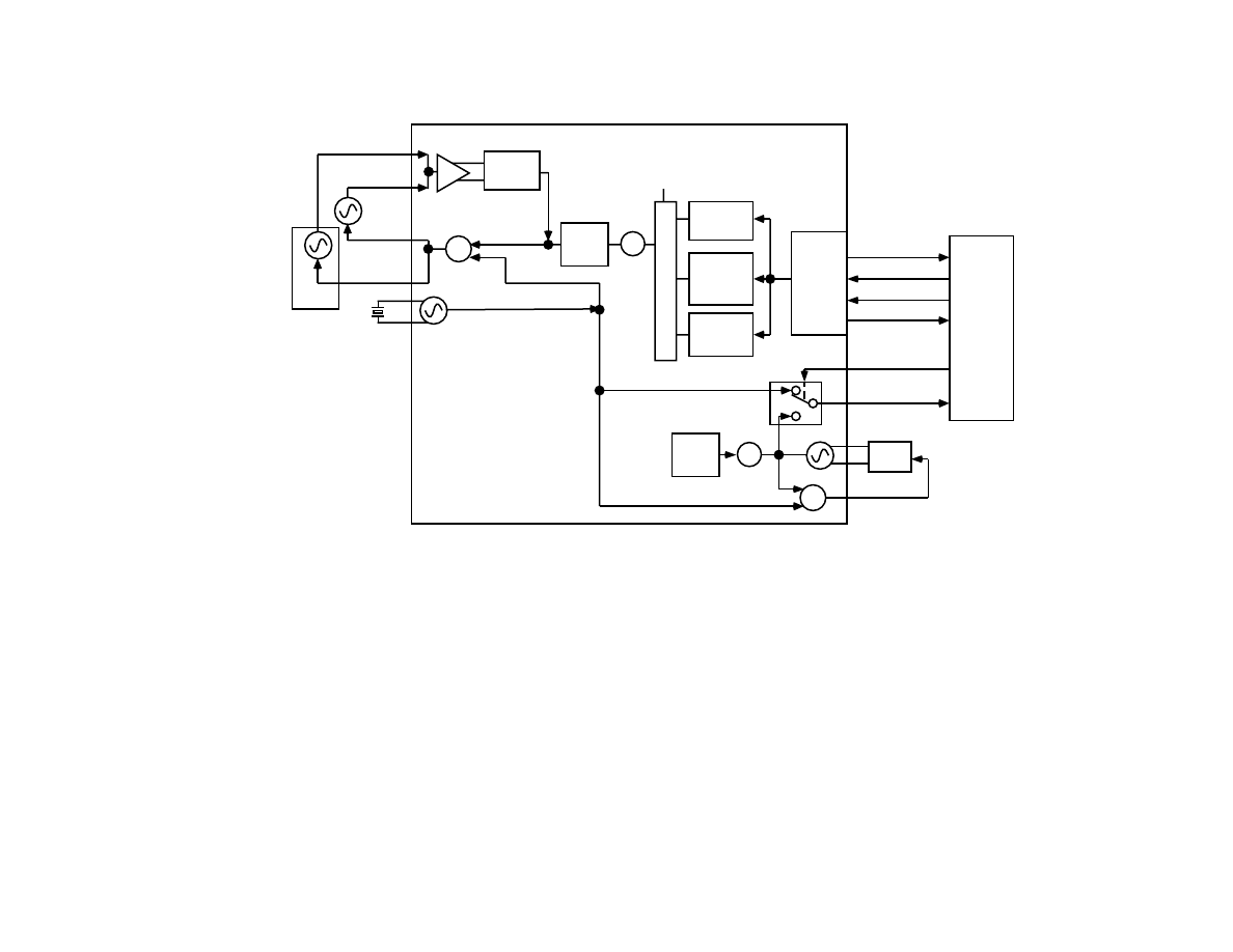
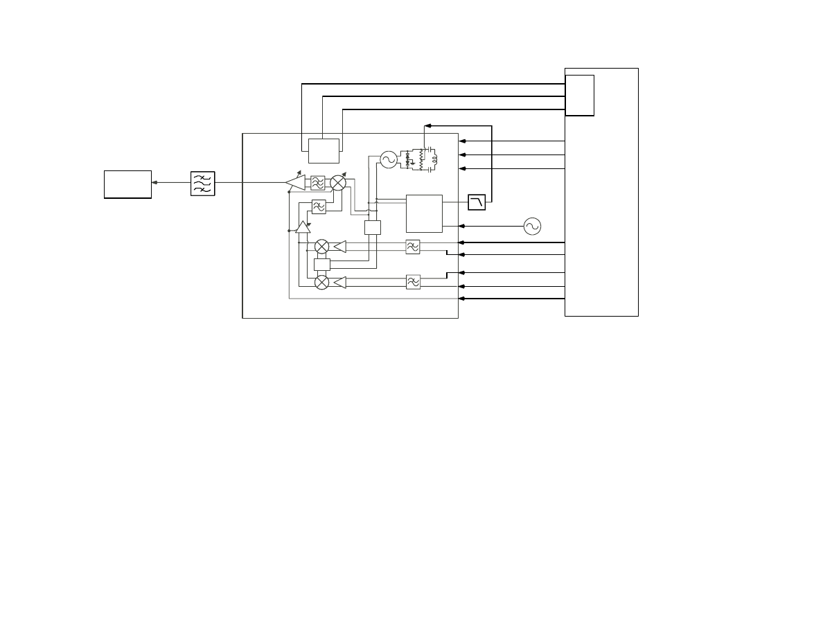
MAGIC LV (Synthesizers/Transmitter)
Description
The MAGIC_LV receives SSI Tx data at DMCS (digital input to start Tx modulation), TXCLK (clock for serial transfer) and SDTX ( serial Tx data) from POG. The
present serial data bit and the three previous data bits are used to set up one of 16 possible waveforms based on the sum of Gaussian pulses stored in a look up ROM.
The resulting signal will then be clocked out at a 16x over-sampling rate. This data pattern input to three-accumumalator fractional N synthesizer with a 24-bit resolu-
tion. The VCO control lines must have compliance over an output voltage range of 0.3VDC to Vcc-0.3V. The charge pumps will have their own supply pin. The voltage
on this pin is expected to be 2.775V typically to obtain sufficient compliance. This will drive external loop filters, which will in turn drive external VCOs. A dual port
modulation mode is obtained with a 9 bit D/A which follows the modulation look up table output waveform is output on the GPO3 pin.This signal is then coupled into
the loop filter to add in the higher frequency components of the modulation which may have been attenuated in the main PLL path. This will allow the use of a lower
bandwidth main PLL to improve the spectral purity of the transmit signal.For EGSM the synthesizer output is 880 - 915MHz, DCS is 1710 - 1785MHz with GMSK mod-
ulation and is directly amplified to the transmitter output.
The prescaler for the main LO is able to accept input frequencies as high as 2.0GHz. The level of this signal shall be between -20dbm and -10dbm. There are two
prescaler inputs to this point each has a 100W resistor in series between the pin and the actual prescaler input.
The reference oscillator is a free running 26MHz crystal. AFC is provided through the SPI bus as a programming offset to the fractional N division system. Since the
26MHz crystal is not locked to the AFC, a second fractional divider system is necessary to derive an accurate 200KHz system reference. This reference is then multiplied
in a PLL to 13MHz for use as an accurate clock to the logic sections of the transceiver.
Motor
o
la
Conf
ide
n
tia
l Pr
opr
ie
ta
ry
4-
10
Ø
PLL_CP
3 Acc
FN Seq
Gen
Σ
BB_CLK_13M
CLK_SELECT
FL510
Ø
CP_TX
PRSC
TX Data
Interface
GSM
Look-up
Table
GSM
Pre-Distort
Σ
3 Acc
FN Seq
Gen
RX_VCO_OUT
TX_VCO_PRSC
TXCLK
DMCS_MAGIC
SDTX
BFSX
AMPS
Interpolator
RX_VTUNE
POG
Y500
MAGIC LV
U500
(Synthesizer Section)
Mod_sel
LIFE
TX
VCO
26MHz
A835:
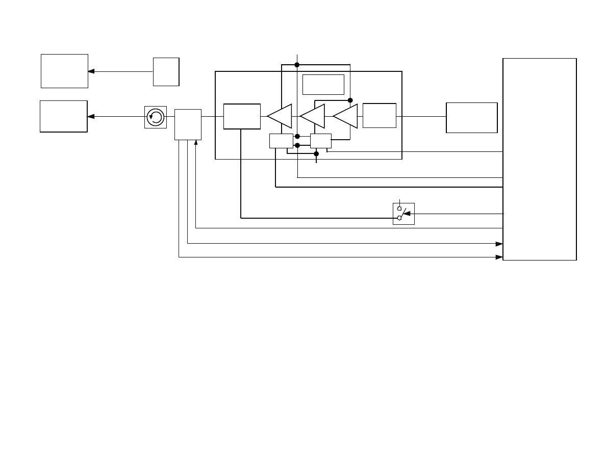
GSM TX VCO
Description
The VCO frequencies are 897 - 1880MHz, handling the three technology bands. The technology bands are controlled by MAGIC_LV via the data lines: N_BAND_0 and
N_BAND_1. CP_TX and GPO3 provides a dual port modulation mode for the TXVCO. N_BAND_0 and N_BAND_1 will select which VCO band will be activated.
GSM_EXC_EN and N_GSM_EXC_EN will enable the buffer stage of U570. TX_EN is activated prior to enabling the buffer and PA. TX_VCO_PRSC is fed back to the
MAGICLV for proper PLL operation. The output frequency for GSM is TX_LOW_RF and PCS / DCS is TX_HIGH_RF. The charge pump output (CPTX) from
MAGIC_LV is the input (VT) for the VCO.
Motor
o
la
Conf
ide
n
tia
l Pr
opr
ie
ta
ry
4-
12
TX_VCO_PRSC
TX_HI_RF
TX_LOW_RF
Tank
Ckt
CP_TX
Loop
Filter
Decoder
N_BAND_0
N_BAND_1
TX_EN
Q500
MAGIC LV
POG
GPO3
GSM_EXC_EN
N_GSM_EXC_EN
RF_TOP
Section
SF_OUT
U570
TXVCO
Delay
FN
9 bit
Dual Port
D/A
GMSK
Look-up
Table
Pre-dist
Sys
Mux
DCS/PCS VCO
GSM VCO
A835:
GSM PA
Description
U800 is a tri-band PA module that operates in EGSM, DCS and PCS bands. The nominal expected maximum gain is ~30dB. .
The AOC_DRIVE input from MAGIC_LV controls the PA output. The voltage applied at the pin is proportionally related to the output power of the PA, as the voltage
increases the gain or power level increases. N_BAND_0 is used to select the operating band. LV_EXC_EN will enable PA operation.
The power detector receives the amplified GSM signal at #1 (EGSM_IN), PCS and DCS at pin #12 (DCS_PCS_IN) from the U800. U801 is a dual combination direc-
tional coupler and temperature compensated power detector output. The power detector couples the Tx power input and feedbacks an output DET_AOC to MAGIC_LV.
A comparator within the MAGIC LV will sample DET_AOC and based on the power amplifier ramps will provide any necessary control voltage adjustments to
AOC_DRIVE The DET_REF is a reference voltage to MAGIC_LV. Expected nominal loss is <. 3dB.
Motor
o
la
Conf
ide
n
tia
l Pr
opr
ie
ta
ry
4-
14
TX_LOW_RF
TX_HI_RF
N_BAND_0
AOC_DRIVE
PA_BATT+
DET_AOC
DET_REF
DCS_PCS_TX
GSM_TX
LV_EXC_EN
FL020
TX_VCO
MAGIC LV
RF
TOP
U800
U801
A835:
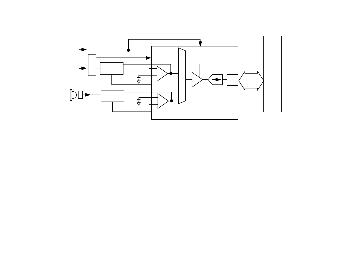
WCDMA Zero-IF Receiver (MAX2396)
Description
The Max2396 (U300) is a fully integrated direct-conversion receiver IC family for WCDMA applications, targeting the emerging 3GPP market.
The Max2396 provides a complete solution for the 3GPP WCDMA FDD receiver (2110-2170MHz, 3.84Mcps) from antenna to baseband I/Q outputs, eliminating the use
of an off-chip IF SAW filter and of RFVCO.
The MAX2396 receiver IC has over 90 dB of dynamic gain control, partitioned between RF and baseband sections. It consists of an ultra-low current LNA with on-chip
output matching and two-step gain modes. The zero-IF demodulator has a differential circuit topology for best input IP2 and for minimum LO leakage to receiver‘s input.
The channel selectivity is done completely in the baseband section of the receiver with an on-chip low-pass filter. The AGC section has over 50dB of gain control range.
LO quadrature generation is done on-chip trough a divide-by-2 prescaler. The DC-offset cancellation in the I/Q baseband channels is done fully on-chip using a DC servo
loop connected over the AGC section. For large DC-offsets transients, very fast settling time is obtain by automatic optimization of the time-constant of the DC-offset
cancellation circuit.
The AGC ensures that the I/Q inputs to HARMONY LITE are at constant signal level. The IF_AGC line is controlled by HARMONY_LITE with a DC control range of
1.2V to 2.1V.
The MAX2396 includes a 3-wire serial bus for PLL programming and for configuring the different receiver modes. The MAX2396_SHDN* line is used for full device
shutdown and the MAX2396_ILDE* line is used for device idle mode.
RX_RF_ATTEN controls the LNA gain control pin of the MAX2396(U300), allowing high gain mode operation for low RF signal conditions and low-gain mode for
high RF signal conditions. IF_ATTEN controls the mixer gain control pin of the MAX2396, allowing high gain mode operation for low IF signals and low gain mode for
high IF signals.
The MAX2396 VCO frequency is controlled by an external phase lock loop (PLL) synthesizer found in the Harmony Lite. The VCO output frequency at RX_PRE_1 and
RX_PRE_2 is through a divide-by-3 prescalar. The VCO output signal is then fed into the PLL synthesizer found in the Harmony Lite. . The internal phase detector
within Harmony Lite drives the charge pump, RX_CP. The RX_CP line drives the tunable resonant network, altering the VCO frequency and closing the loop.
Motor
o
la
Conf
ide
n
tia
l Pr
opr
ie
ta
ry
4-
18
÷2
÷3
SPI
Interface
WB_ASPI_CLK
WB_ASPI_DATA
MAX2391_CS
WB_RXI
WB_RXIX
WB_RXQ
WB_RXQX
MAX2396_SHDN*
MAX2396_IDLE*
Harmony
Lite
Harmony
Lite
Harmony
Lite
RX_PRE_1
RX_PRE_2
Tank
Ckt
RX_CP
RF_TOP
WCDMA_RX
FL300
T300
RX_RF_ATTEN
AGC
IF_ATTEN
REF_15_36

A835:
Harmony Lite (Receive Section)
Description
The HAMONY LITE (U101) handles the backend processing of the WCDMA in phase (RX_I+, RX_I-) and quadrature (RX_Q+, RX_Q-) signals from the demodulator.
The HARMONY LITE performs an analog to digital conversion of gain, phase and DC offset correction of the RX data and sends it to the POG (U1000) via data lines
BBIF_RX(9:0).
The analog I and Q signals are applied to the Harmony Lite IC, which processes the analog baseband portion of the radio. The SOS detector is used as an off-channel
detector to detect the level of undesired interfering signals. It monitors the voltage swing at the input to the baseband filters, and provides a logic level output to the
AGC/RSSI controller to indicate if the level is greater than a threshold specified by SPI bits, which then sets the appropriate gain setting in the front-end and IF
stages.The AGC system provides overload protection for both the strong on-channel signal and the off-channel portion of the signal (interferers) that is present in the RF
receive band. Signal levels are detected at the baseband filter inputs of the Harmony Lite (off-channel detector) as well as after the channel filtering and analog-to-digital
conversion (on-channel detector).The digital AGC/RSSI block controls the bypass mode of the LNA and the IF variable gain amplifier. A digital representation of the
desired received signal strength is sent to the POG via the SPI.
Low pass filtering is performed on the complex I and Q signals, and then applied to the associated 8-bit ADCs and sampled at a rate of 4 times per symbol. A DC offset
correction loop corrects for any DC offsets at the I and Q ADC inputs. A group delay equalizer is employed in the receive signal path following the baseband SRRC filter
to minimize performance loss from the analog active order SRRC channel filter. Gain and phase mismatches between the I and Q channels can affect the detectability of a
WCDMA signal in static and multipath fading conditions due to distortion caused in the QPSK signal constellation map. Thus, I/Q magnitude and phase imbalance cor-
rection circuits are used. At the output of the Magnitude Equalizer, the I and Q values are rounded from 8 bits to 6 bits and then multiplexed and routed to the digital sig-
nal processing circuitry located on the POG IC.
Motor
o
la
Conf
ide
n
tia
l Pr
opr
ie
ta
ry
4-
20
Σ
S/H
DCOC
Group
Delay
Equal.
I/Q
Phase
and
Gain
Equal
Tracking
Loop
SOS
AGC Control
&
Logic
8 bits
Σ
S/H
DCOC
Group
Delay
Equal.
8 bits
Interleave
and
Round
BBIF_RX
(9:0)
BBIF_RX_FRAME
POG
BBIF_CLK
RX_RF_ATTEN
AGC
RX_I+
RX_I-
RX_Q+
RX_Q-
HARMONY LITE
U101
(RX section)
A835:
Harmony Lite (Control Section)
Description
There are several functions that the sequence manager is controlling.
1.
Sequence manager outputs to external devices
2.
On/Off control of clocks, battery save signals etc…
3.
Clock frequency selection for correction paths
4.
DCOC register selection coarse, medium and fine modes
The HARMONY LITE has two sets of SPI interfaces; one set is for handling the control interface for the transceiver (AUXSPI lines) and ones for interfacing with POG
(SPI lines). Further, all SPI interface is generated from POG and written to HARMONY_LITE or parsed through to the MAXIM (U200 & U300) parts.
Layer one timing signals control the functionality of the RF section of the transceiver relative to the air interface. There are three signals defined on each transmit and
receive section of the transceiver. TX_PRE_KEY and RX_ON are asserted before the need to receive or transmit in order to launch the necessary sequence of events to
warm up the required functional blocks. TX_RAMP and RX_AQUIRE are asserted when actual transmission and reception are to begin. RX_SLOT and TX_SLOT are
used during continuous transmission and reception to trigger events that must be aligned with slot boundaries. It‘s important to reiterate, the TX_RAMP directly corre-
sponds to the PA turning on and RX_AQUIRE corresponds to data being sent to the WCSP.
Motor
o
la
Conf
ide
n
tia
l Pr
opr
ie
ta
ry
4-
22
MAX2396_SHDN
MAX2396_IDLE*
MAX2391_CS
MAX2396_LOCK
HL_TX_EN
SPI/
Sequence
Manager
VGC
VGC2
VMODE
PABIAS1
PABIAS2
RF_DETECT
TEMP_COMP
MUX
2361_SHDN
TX_STBY*
V_DETECTOR
SPI_CE
SPI_DATA_IN
SPI_DATA_OUT
WB_SPI_CLK
PORB
WB_RX_ON
WB_RX_SLOT
WB_RX_ACQ
WB_TX_PRE_KEY
WB_TX_SLOT
WB_TX_RAMP
AOC_PWR_UP_DOWN
WB_ASPI_CE_2
ASPI_DATA
ASPI_CLK
2361LOCK
WCDMA
TX
WCDMA
RX
POG
WCSP
RF_RESET*
Harmony Lite(U101)-Logic Section
SM
O_3
SM
O_5
SMO_9
GPI_1
SMO_15
SMO_21
2361_CS*
SMO_23
HARMONY_CS
WB_SPI_MOSI
WB_SPI_MISO
A835:
Harmony Lite (Synthesizer Section)
Description
The clock source for the Harmony Lite (HLite) is a 15.36Mhz oscillator (TCXO). Y130 is used to generated the 15.36MHz clock source. AFC for Y130 is controlled by
the Harmony Lite sequence manager via the AFCDAC line. The 15.36MHz clock source is enabled by an internal SPI bit and external control signal coming from
15.36M_CLK_EN*). The 15.36MHz clock source provides clocks to all A/Ds, DACs, external references and internal digital circuits of the Harmony Lite. In addition,
clock references are generated for the RAINBOW, WCSP, RX and TX RF circuits.
The WCDMA VCO, integrated in U300, has a frequency range of 2.3G thru 2.36GHz, supplying the receiver with an LO. The LO signal is generated for the receiver by
using a phase locked loop (PLL) architecture integrated in the Harmony Lite. The phase locked loop uses a fractional loop divider to permit fast lock times and low phase
noise on the output signal. The control range is controlled by HARMONY_LITE with a control range between 0.5 - 2.5V, with an output power @ ~-3 - 3dBm. The VCO
output frequency is fed into a prescalar and devided down into a desired comparison frequency. The 15.36MHz reference frequency is also divided down into a compari-
son frequency. The two divided frequencies are then compared with a phase detector. The phase detector will then drive the charge pump. The charge pump output is pro-
cessed by the external loop filter and drives the tunable resonant network, altering the VCO frequency and closing the loop.
The superfilter block is used to provide a filtered supply voltage to the WCDMA VCO.
Motor
o
la
Conf
ide
n
tia
l Pr
opr
ie
ta
ry
4-
24
TCXO_EN_IN
TCXO_EN_OUT
VRF_RX_2_775V
AFCDAC
SPI/
Sequence
Manager
Q130
Y130
REF_OSC_15_36M
U300
Prescaler
Ø
Charge
Pump
Super
filter
A/N
Counters
/R
REF_OSC_IN
CLK
GEN
REF_H_A
÷1,2,4,16,32
CLOCK_OUT
WCDMA
TX
WCDMA
RX
BB_CLK_15.36M
POG
BLUETOOTH
U5600
REF_FREQ
Harmony Lite
U101
(
Synthesizer Section)
BLUETOOTH
WCDMA TX
Modulator
U200
TCXO_REF
A835:
Harmony Lite (TX Section)
Description
The BBIF(BBIF_TX) is the transmit data path for transferring digitally sampled I / Q data from the POG. The demultiplexing unit performs the I/Q deinterleaving func-
tion to supply separate I and Q channel data into the transmit FIR filters. The FIR filter design is used to meet 3GPP spec requirements of simultaneous transmission of a
pilot channel and of multiple data channels each requiring a different spreading code and each requiring separate power control. The PN sequence generator provides I/Q
interleaved 8-bit PN data into the demultiplexing section. The DC correction(DCOC) block is able to correct for DC offsets due to the D/A‘s, anti-aliasing filters, and
transmit FIR filters in a feedback control loop. A mixed mode control loop located at the output of the transmit FIR filter is employed to correct DC offsets and I/Q gain
imbalances, i.e. DCOC and I/Q Phase and Gain equalizer. The outputs of the I/Q gain equalization unit is fed into 10-bit I and Q DAC‘s. The programmable gain anti-
aliasing filters, or TX smoothing filters, accepts differential I/Q signals of DC to 1.92MHz frequency components from the D/A Converters to attenuate the unwanted
clock signals of 15.36MHz and to smooth the signals for the TX modulator(MAX2363). The output of the TX smoothing filters are then fed into a multiplexed 6-bit A/D
with sample/hold scheme. This gives the information of the amplitude and the DC common mode voltage from the I / Q Tx filter outputs by a single Analog-to-Digital
Converter (ADC) as the part of digital correction loop.
The differential TX I and TX Q signal are finally fed into the TX modulator(MAX2363).
Motor
o
la
Conf
ide
n
tia
l Pr
opr
ie
ta
ry
4-
26
S/H
I/Q
Phase
and
Gain
Equal
10 bits
S/H
DCOC
10 bits
Demux
BBIF_TX
(9:0)
TX_I+
TX_I-
TX_Q+
TX_Q-
BBIF_TX_FRAME
HARMONY LITE
U101
(TX section)
PN Seq
Gen.
Tracking
Loop
Demux
Mux
FIR
FIR
WCDMA
TX
BBIF_CLK
POG
U1000
A835:
TX Modulator (MAX2395)
Description
The MAX2395 is a fully monolithic quasi-direct modulator IC for use in WCDMA/UMTS transmitters. The quasi-direct modulation architecture reduces system cost,
component count, and board space compared to transmitters using IF SAW filter with IF VCO and IF synthesizer blocks.
The MAX2395 includes I/Q baseband filters, an IF I/Q modulator with VGA, a fully monolithic VCO with PLL, a up-converter mixer with VGA, and a power amplifier
driver. The differential baseband I/Q signals are modulated onto a variable-IF carrier in the 384 396MHz band; The IF signal is then up-converted to the 1920 - 1980MHz
band. On-chip Image rejection in the 2688 - 2772 MHz frequency band is done with an integrated notch filter. The RF VGA and IF VGA provide a nominal 90dB of out-
put power control. The use of the quasi-direct modulator scheme ensures excellent carrier suppression over the total power control range. In addition, only one on-chip
VCO and one integer-N PLL are needed to generate both LO signals for the IF and RF sections. The on-chip component matching by monolithic integration at IF fre-
quencies results in excellent phase accuracy and amplitude balance.
The PLL operation is programmed by loading data on the SPI/Microwire compatible 3-wire serial bus. In addition, the WCDMA required compressed mode can be
selected via an external IDLE pin. The IC operates from a single 2.7V - 3.3V supply.
Motor
o
la
Conf
ide
n
tia
l Pr
opr
ie
ta
ry
4-
28
VGC
WB_TXI
WB_TXIX
WB_TXQ
WB_TXQX
WB_ASPI_CLK
WB_ASPI_DATA
WB_ASPI_CE2
Harmony Lite
U101
SPI
Serial
Bus
/2
/3
RF
Integer-N
PLL
2340MHz
390MHz
TCXO_REF
Y130
TX SAW
FL401
1920-1980MHz
POUT
MAX2395
U200
PA
SHUTDOWN
IDLE
LOCK
Bias
Output
Match
Interstage
Match
Bias
Input
Match
A835:
WCDMA PA
Description
U400 is a three-stage power amplifier handling the band of WCDMA Tx frequencies between 1920 - 1980MHz. The nominal expected maximum gain is ~30dB.
HARMONY_LITE controls the RF biasing of the amplifier at PA_BIAS1 and PA_BIAS2 with a control range of 0 - 2.5v. HARMONY_LITE also controls VLD for PA
load switching. PA load switching in WCDMA is vitally important to conserve battery life and to avoid unnecessary radio interference with base stations. When VLD is
at a low state (0v), the transmitter is in high power mode, consuming higher current but with overall better PA performance. When VLD is at a high state, the transmitter
is in low power mode, consuming less current with overall poor PA performance. In theory, as the Tx power level increases or decreases beyond a certain power thresh-
old, VLD is enabled or disabled. As Tx power decreases (as requested from a base station) down to ~14.5dBm, VLD will switch high. If Tx power is requested to
increase beyond ~19dBm, VLD is switched low.
The power detector receives the amplified WCDMA RF signal at RF_IN from the PA. U407 is a combination directional coupler and temperature compensated power
detector with a differential output. The power detector couples the TX power input and feedbacks an output RF_DETECT to HARMONY LITE. The TEMP_COMP
also obtains the coupled power but removes the RF signal content, leaving a DC level. The DC level is feedback to HARMONY LITE. Expected nominal loss is <. 3dB.
The isolator (FL404) provides isolation between Front-End Module (FEM) and transmitter path. Nominal insertion loss is ~ 0. 55dB.
Motor
o
la
Conf
ide
n
tia
l Pr
opr
ie
ta
ry
4-
30
Temp
Sens
U406
Isolator
FL404
PA BIAS1
VMODE
RF_ DETECT
PA BIAS2
V_DETECTOR
VRF_TX_2.775V
VLD
TEMP_COMP
TEMP_SENSE
PCAP
U3000
RF TOP
PA_ENABLE
Q401
Harmony Lite
U101
Coupler
/ RF
Detector
U407
MAX2395
U200
WCDMA_TX
POUT
BATT+
U400
PA2001_5W
VRF_REF_2_775V
A835:
Charger
Description
The majority of the charging circuit is integrated in PCAP. This includes a digital to analog converter, analog to digital converter, battery feedback switch, thermistor
switch/pullup, and current control sense. External FETs (Q3966 and Q5400) are provided to enable/disable EXT_B+ and BATTERY supply paths to radio circuitry
(B+). An external sense resistor (R3961) and a charging FET (Q3960) are provided to control charging current between EXT_B+ and BATTERY.
Due to pin count constraints on the CE bus, the Charger Identification input signal and Battery Feedback output signal share the same accessory connector pin. Software
will first detect the Charger ID Voltage (AD6) before enabling the Battery Feedback Voltage via the Battery Feedback Switch in PCAP. The Battery Feedback switch
must not be enabled at any time for an accessory that is not a valid Fast Charger.
Battery Feedback Voltage provides a reference voltage to the external power supply during charging. The battery feedback switch is needed to remove the battery feed-
back voltage from the feedback loop of the AC/DC Adapter or VPA when charging is complete or after a fault has occurred. This switch will be enabled before the char-
ger DAC is programmed when charging is to begin. Battery feedback will turn on before the charger is enabled. The charger will be turned off before battery feedback is
disabled.
A thermistor in the battery package is used to determine cell temperature of the battery pack before charging begins. The battery EPROM (BATT_IO) will contain
limit parameters that determine the minimum and maximum temperatures at which charging can occur.
PCAP has an integrated over-voltage detection circuit that provides protection against damage caused by external charger voltages exceeding 7.0Vdc. If an over-voltage
condition occurs, the EXT_B+ FET (Q3963) will be disabled. This will prevent high voltage (>7Vdc) from being applied to radio circuitry (B+).
Mid-rate charging is supported if a valid mid-rate charger and valid battery are detected. A mid-rate charger will source up to 400mA of current to the radio circuitry and
charging circuitry during idle mode. The mid-rate charger will supply 5.9Vdc (up to 400mA) to the phone, regardless of the BATT_FDBK voltage. If the phone is
in transmit mode, mid-rate current will be supplied to the battery and radio circuitry via the charging path only (EXT_B+ FET (Q3966) will be disabled via the
MIDRATE_1 line). Dead battery TX operation or ‘No Battery’ operation is not supported with a mid-rate charger.
Motor
o
la
Conf
ide
n
tia
l Pr
opr
ie
ta
ry
4-
32
RAW_EXT_B+
EXT_B+
B+
ISENSE
CHRGC
BATT+
MAIN_FET
BATT+
Q3966
Q3967
R5480
CR3961
R3961
Q3960
CR3960
Q5400
Q3963
OV_GATE
OV_SENSE
PCAP
U3000
MIDRATE_1
PCAP
U3000
CE
Conn
Charger
BATT_FDBK
AD6
BATT_THERM
CE
Conn
SPI
MUX
BattSense
BATT_IO
POG
Batt
Conn
SPI
Q5401
BATT_FDBK_SW
A835:
Voltage
Regulators
Description
Voltage regulation is provided by the PCAP IC (U3000). Multiple regulators are used to provide better isolation between sensitive load circuitry and noisy circuitry.
The regulators and their load circuitry are described below:
· VBOOST_LX(VBOOST_5_5V) - VUSB abd V10 input voltage regulator
· VBUCK_LX(VBUCK_2_25V) - V1, V3, V4, and V7 input voltage regulator
· V_VIB - Vibrator
· Vsim2(VSIM) - SIM card interface
· Vaux1(VRF_TX_2_775V) - HV I/O, Display(20), Imager(12), GPS Baseband(8), GPS Flash,
· Vaux2(VRF_RX_2_775V) - RF RX circuits
· Vaux3(VMMC_2_8V) - SD Flash
· VUSB - PCAP USB xcvr
· V1(VMEM_1_875V) - Baseband Processor Flash Core
· V2(VA_2_775V) - Audio
· V3(VLVIO_1_95V) - Magic LV I/O,
· V4(VRF_REF_1_875V) - RF reference
· V5(VGPS_RF_2_775V) - GPS RF
· V6(VHVIO_2_775V) - RF TX circuits
· V7(VRF_DIG_1_875V) - RF digital
· V8(VBLUETH_1_875V) - Bluetooth
· V9(VRF_REF_2_475V) - RF Reference
· V10(VRF_HV_5V) - RF HV
Motor
o
la
Conf
ide
n
tia
l Pr
opr
ie
ta
ry
4-
34
VSIM
VTR1_2_8V
VBUCK_2_25V
VBOOST_5_5V
VA_2_775V
VGPS_RF_2_775V
V_VIB
VRF_REF_2_475V
B+
LX3
LX1
V2
V5
V9
V_VIB
Vsim2
Vaux3
VMEM_1_875V
VLVIO_1_875V
VRF_REF_1_875V
VRF_DIG_1_875V
VBLUETH_1_875V
Vaux1_ Drv
Vaux1
B+
Vaux2_ Drv
Vaux2
B+
VRF_HV_5V
B+
VMAIN_1_55V
U3206
PCAP
PCAP
V1
V3
V4
V7
V8
V10
VUSB
VUSB
PCAP
VHOLD_EXT_EN
Q3610
Q3502
VRF_TX_2_775V
VRF_REF_2_775V
VRF_RX_2_775V
Switcher
Supply
VHVIO_2_775V
V6_ Drv
V6
B+
Q3403
Q3961
U3700
B+
VCAM_3V
VID_GPSb_SEL
POG
VSIM
VSIMC
A835:
RX Audio
Description
Receive audio data is transferred from the POG to the PCAP through the ASAP interface for mono audio and the VSAP interface for stereo audio data. The data is then converted
into an analog form through a 16-bit Stereo DAC or 13-bit phone DAC. The output of PCAP’s internal DAC drives the internal PGA. The output of the PGA can be routed to one
of the four supported outputs via the internal multiplexer. All outputs use the same D/A converter so only one output can be active at one time. The user can adjust the gain of the
audio outputs with the volume control buttons.
The Handset Speaker is driven by PCAP’s internal SPKR differential amplifier. Following the speaker path from the PCAP pins SPKR- and SPKR+, they are routed through
R4004 and R4005 respectively, and then connected to the transducer. Off the SPKR- path, SPKR_IN is routed through C4002 for the inverting input of the speaker amp A1.
SPKR_OUT1 from PCAP is routed through C4000 and C4002 to SPKR- which is the DAC output of the CODEC. SPKR_IN and SPKR_OUT1 will output their respective bias
voltages on these pins during standby times. This is to maintain the voltage across an external coupling capacitor to avoid audio “pops” when the amplifier is enabled.
The headset uses a standard 2.5mm stereo phone jack. The phone will detect the presence of a stereo headset using HS_SPKR_L of the headset jack, which is pulled high by
R4395 and connected to the ST_COMP of PCAP (this is an interrupt of PCAP which gets sent to MCU over the SPI bus). This pin will be pulled to a logic low whenever the ste-
reo headset plug is inserted into the jack. The headset may contain a momentary switch, which is normally closed and is in series with the microphone cartridge. When the
momentary switch is pressed, the bias current being supplied to the microphone will be interrupted. The phone will detect this action and make an appropriate response to this
action, which could be to answer a call, end a call, or dial the last number from scratchpad.
The Headset Speaker is driven by PCAP’s internal Left and Right amplifier. Following the speaker path from the PCAP pins ARight_Out and ALeft_Out, they are routed through
C4356, R4352 and C4306, R4302 respectively, and then connected to the headset jack. Off the ARight _Out path, AR_IN is tapped off through C4354 for the inverting input of
the audio amp ARIGHT. Off the ALeft_Out path, AL_IN is tapped off through C4304 for the inverting input of the audio amp ALEFT.
The External Speaker is connected to pin 15 of J5000 (AUDIO_OUT), the accessory connector for the mobile phone. The audio path is routed through R4400 and C4400 and
connected to EXTOUT of PCAP. The DC level of this Audio_Out signal is also used to externally command the phone to toggle it’s ON/OFF state. The Audio_Out signal con-
nects to PCAP’s ON2 pin via R5053 to provide this capability. When a DC level of <0.4V is applied by an accessory for a minimum of 700 milliseconds on the Audio_Out line,
the phone will toggle it’s ON/ OFF state.
The Loadspeaker is driven by PCAP’s ALRT amplifier (A2). The alert path from the PCAP pins ALRT- and ALRT+ are routed directly to the alert transducer. Off the ALRT-
path, ALRT_IN is routed through R4201 for the inverting input of the alert amp A2. SPKROUT2 from PCAP is routed through C4200 and R4200 to ALRT- which is the DAC
output of the CODEC.
Motor
o
la
Conf
ide
n
tia
l Pr
opr
ie
ta
ry
4-
36
PCAP
SPKROUT2
ALRT_IN
EXTOUT
Audio Filter
Circuit
ALRT-
ALRT+
Loudspeaker
ON2
R5053
POG
SSI
ASAP_TX
ASAP_RX
ASAP_CLK
ASAP_FS
13-bit
Phone
DAC
16-bit
Stereo
DAC
J5501
J5500
ARIGHT_IN
ARIGHT_OUT
PGA
R
L
SUM
PGA
ALEFT_IN
ALEFT_OUT
Audio Filter
Circuit
Audio Filter
Circuit
HS_SPKR_L
HS_SPKR_R
ST_CMP
ST_REF
R4395
Stereo
Headset
SSI1
SPKROUT1
SPKR_IN
Audio Filter
Circuit
SPKR-
SPKR+
Handset
Speaker
A
UD MUX
SSI
SSI2
MMSAP_FS
MMSAP_CLK
MMSAP_TX
A1
AUDIO_OUT
A2
A4
ALRT-
ALRT+
J4000
J4001
EARSPKR-
EARSPKR+
J4300
FL4300
FL4000
A835:
TX
Audio
Description
The Internal Microphone is a single ended part. Following the Internal microphone path, the microphone is biased by R4103 to provide a MIC_BIAS of 2.0V from pin
MIC_BIAS1 of PCAP. C4198 is connected to MIC_BIAS1 and MB_CAP1 pin on PCAP to bypass the gain from the VAG to MIC_BIAS1 which keeps the noise balanced. From
there, the signal is routed through C4100 to AUX_OUT pin on PCAP, bypassing the input to the A5 amplifier.
The headset microphone path (HS_MIC) is biased through R4396 and R4392, which is connected to pin MIC_BIAS2 on PCAP and bypassed with C4199 connected to pin
MB_CAP2. From here the signal is routed through C4395 and R4388 to MIC_IN- pin on PCAP, which is the input to the A3 Amplifier. The Microphone path is tapped off after
R4388 before the MIC_IN- input to R4389 connected to the MIC_OUT pin on PCAP, which is the output of the A3 Amplifier. The HS_MAKE_DET line monitors the presence
of a headset by detecting the voltage at A1_INT of PCAP, which passes through R4398. A switching mechanism integrated in the headset jack will open or close the
HS_MAKE_DET path to ground, depending on whether the headset is attached or not.
The External Microphone input (AUDIO_IN) is connected to the accessory connector for the mobile phone. The path is routed through L4400, C4401 and R4401 to the
EXT_MIC pin on PCAP. This signal feeds directly to the input multiplexer without an intervening gain stage. In addition to audio signals, AUDIO_IN supports detection of
accessory devices. The accessory attached to the CE bus shall have an output impedance that will load LOGIC_SENSE to a predetermined level. The POG will read the input
level of LOGIC_SENSE and configure the audio accordingly.
The proper Microphone path is selected by the AUD MUX controller and path gain is programmable at the PGA. The A/D converter willl convert incoming analog signals into
13-bit, 2's compliment, linear PCM words. The digital audio signals are then transferred to the POG DSP through a four wire serial interface (ASAP).
Motor
o
la
Conf
ide
n
tia
l Pr
opr
ie
ta
ry
4-
38
MIC GAIN
PCAP
LOGIC_SENSE
MIC_BIAS1
AUX_OUT
AUX_MIC-
Audio Filter
Circuit
MIC
ADC
POG
PGA
AUDIO_IN
MIC_BIAS2
MIC_OUT
Audio Filter
Circuit
A
UD MUX
HS_MIC
SSI
ASAP_RX
ASAP_FS
ASAP_CLK
NC
J4300
J4100
A5
A3
HS_MAKE_DETECT
EXT_MIC
NC
VAG
A835:
PCAP
Description
The Platform Control Audio Power IC (PCAP), U3000, is a mixed signal IC that contains the following features:
·
Audio input/output amplification and filtering
·
Audio path selection
·
Voltage regulation
·
Battery charging control
·
Real time clock
·
Ringer/vibrator control
·
RS-232/USB drivers
·
Back-light control
·
Status LED control
·
Multiplexed DAC inputs for temperature and voltage monitoring
·
Dual SPI control interface to allow access from two independent baseband processors
·
Stereo DAC
·
Overvoltage protection
·
Touch Screen
The PCAP IC is controlled and configured by the Baseband Processor IC through a four-wire SPI interface. The Baseband Processor has read/write access to the PCAP
IC. Audio data is transmitted/received via the Baseband Processor through a four-wire SSI interface.
Motor
o
la
Conf
ide
n
tia
l Pr
opr
ie
ta
ry
4-
40
Baseband
Circuits
RF Interface
Logic Interface
Regulator
Interface
Backlight
Status
LEDs
Linear
Regulators
Control
Logic
Switching
Regulator
LED
Drive
Backlight
Control
POG
Power Cut
Power Fail
Handling
XTAL
Coin Cell
Interface
Speaker Ckts
Mic Ckts
Charger
Logic
Interface
POG
SPI
Interface
Charger
Control
Multiplexer
Audio
Amplifiers
USB
RS232
Bus
CODEC
A/D
SSI
Interface
Overvoltage
Protection
CE Bus
POG
Headset
Stereo Detect
USB
On-the-Go
CE Bus
POG
Bluetooth
U3000
Display
Touch
Screen
Interface
A835:
POG
Description
The POG(baseband processor) integrates a 32-bit RISC Communications Engine (MCU), a 32-bit DSP Core and an Interprocessor Communications Module (IPCM)
along with associated peripherals and co-processors. The following provides a brief description of the cores and associated peripherals being used in this design.
·MCU – Micro Controller
·DSP for GSM Signal processing
·EIM(external interface module) interfaces to FLASH and DRAM
·USB/Serial Communications
·GPIO - For A/Ds
·IPCM which provides a multichannel DMA between the Mcore, DSP and peripherals.
·WCSP Interface
·GQSPI - PCAP Interface
·EBIF(External Bus Interface) DMA – WCDMA Data Transportation
·MQSPI1(Qued Serial Peripheral Interface) – WCDMA Control Signals
In addition to POG’s internal memory system, the architecture provides 128Mbits (16M byte) of external flash memory via two Intel Danali 64M bit parts. The memory
bus is 23 address bits and 32 data bits. The flash memory runs at 42-45MHz.
Motor
o
la
Conf
ide
n
tia
l Pr
opr
ie
ta
ry
4-
42
MCU
M341
DSP
Starcore
MDI
IPCM
RISC
VSAP
EL1T1
EL1T2
MQSPI1
MQSPI2
Serial BBIF
ASAP
UART1
UART3
UART2
SIM
MMC
IrDA
USB
LCD
GQSPI
WCSP
Magic LV
(GSM)
Harmony
Lite
(WCDMA)
80kB
eDRAM
GPIO
EBIF
CKIH
PCAP Codec
USIM
PCAP
CE Bus
MUX
Mux
Nexus
JTAG
cache
128Mbit
FLASH
Keypad
1-wire
Misc
POG
·EL1T1(Enhance Layer Timer) – WCDMA Event timer
·CKIH - WCDMA 15.36MHz clock
·GPS Interface
·USIM interface
·ASAP interface for PCAP and Bluetooth audio interface
·Serial BBIF(Baseband Interface) – GSM Data Transportation
·MQSPI2(Qued Serial Peripheral Interface) – GSM Control Signals
·EL1T2(Enhance Layer Timer) – GSM Event timer
·CKIH - GSM 13MHz clock
GPS
SDRAM
EIM
MUX
64Mbit
SDRAM
USB_DM
USB_DP
BLUE_CLK_EN*
BLUE_WAKE*
BLUE_HOST_WAKE*
A835:
Bluetooth IC
Description
The BCM2035 has an integrated radio transceiver that has been optimized for use in 2.4 GHz Bluetooth wireless systems. It has been designed to provide low-power,
low-cost, robust communications for applications operating in the globally available 2.4 GHz unlicensed ISM band. It is fully compliant with the Bluetooth RF Specifica-
tion v1.1 and meets or exceeds the requirements to provide the highest communication link quality of service.
The receiver has a high degree of linearity, an extended dynamic range, and high order on-chip channel filtering to ensure reliable operation in the noisy 2.4 GHz ISM
band. The BCM2035 also features a fully integrated transmitter. Baseband data is GFSK modulated and upconverted to the 2.4 GHz ISM band via an internal mixer. The
output Power Amplifier (PA) provides a nominal power output of 0 dBm and has a power control to provide 24 dB of gain control in 8 dB step sizes. Local Oscillator
(LO) generation provides fast frequency hopping (1600 hops/second) across the 79 maximum available channels.
The uPU runs software from the Link Control (LC) layer, up to the Host Controller Interface (HCI). The microprocessor is an enhanced performance 8051 micro-
controller.
The BBC manages the buffering, segmentation, and routing of data for all connections. It also buffers data that passes through it, handles data flow control, schedules
SCO/ACL TX/RX transactions, monitors Bluetooth slot usage, optimally segments and packages data into baseband packets, manages connection status indicators, and
composes and decodes HCI packets.
The Peripheral Transport Unit (PTU) handles the Device Interface. The PTU supports three types of devices: USB, UART, and PCM.
The PMU provides power management features that can be invoked by either software through power management registers, or “packet handling” in the baseband core.
Motor
o
la
Conf
ide
n
tia
l Pr
opr
ie
ta
ry
4-46
uP Unit
(UPU)
Peripheral
Transport Unit
(PTU)
2.4GHz
Transceiver
Frequency
Synthesizer
REF_OSC_15_36M
Harmony
Lite
POG
PCAP
ASAP_RXD
ASAP_TXD
ASAP_FS
ASAP_CLK
CLK_32_768K
Power
Management Unit
(PMU)
Bluetooth
Baseband Core
(BBC)
BLUETOOTH
IC
U5600
BT_RF_ANT
HELEN
A835:
GPS
Description
The 1575.42 MHz satellite signal can be received through the GPS antenna PIFA_Planar Inverted F Antenna) or exernal GPS antenna. GPS signal received through the
PIFA will pass through FL6055 and LNA U6051. The signal is then passed to the LNA input of U6050 through FL6050.
The input signal at the LNA of U6050 is a Direct Sequence Spread Spectrum (DSSS) signal at 1575.42MHz with a 1.023 Mbps Bi-Phase Shift Keying (BPSK) modulat-
ed spreading code. The DSSS signal is then injected into an image reject mixer. The Mixer and on-chip 1565.97 MHz VCO will produce an IF center frequency of
9.45MHz. An IF filter is required between the Mixer and AGC Amplifier to provide an anti-aliasing function before A/D conversion. The IF filter block also contains an
I-Q phase shift combiner. This circuit properly phase shifts and sums the I and Q outputs from the image reject mixer to a single channel. The AGC amplifier provides
the additional gain needed to optimally load the signal range of the 2-bit A/D Converter. The 2-bit A/D onverter will then provide signal and magnitude output bits to the
Interface Block. The outputs of the Interface Block provide clocks and the 2-bit sample data to the CGSP2e/LP(U6000). These signals use single-ended PECL(Positive
Emitter-Coupled Logic) signaling to simplify the complexity of this interface. The interface block inputs are the single-wire AGC interface, (AGCDAT) and the Power
Control pin (PWRCTL).
The GPS DSP within U6000 correlates the incoming MAG and SIGN data. Wide parallel search architecture enables simultaneous search of 1,920 time/frequency bins
which enables a powerful combination of very fast reacquisition along with the capability to find and track very weak signals. The UART residing in U6000 is used to
interface data information between the GSP2e/LP(U6000) and POG. An integrated GPIO unit provides support for a variety of peripherals.
RTC is an ultra-low power implementation of a high precision 32-kHz driven clock derived from the PCAP. It is separately powered by the VDDRTC to allow maximum
battery life by maintaining time for the next power on. REF_FREQ is used as an external clock source for U6000.
GPS_WAKEUP* is an active low signal from POG to wake up SiRFLoc client from the deep sleep mode. GPS_RESET* is an active low hard reset signal for the SiRF
BB IC and Flash. GPS_BOOT_SEL is used by POG to set boot configuration upon reset. GPS_TIME_SYNC is an active high signal to provide time stamping of the pre-
cise time aiding that is sent over from POG over the UART.
Motor
o
la
Conf
ide
n
tia
l Pr
opr
ie
ta
ry
4-
48
GPS ANTENNA
PIFA
M6050
EXT GPS
ANTENNA
FL6055
U6051
FL6050
÷41
ø
÷7
÷9
X2
Y6050
24.5535MHz
I
Q
IF Filter
&
IQ Combiner
AGC
A/D
MAG
SIGN
AGCDAT
ACQCLK
GPSCLK
Bias
Control
GPS_GPIO3
38.194MHz
49.107MHz
U6050
SiRF
RF to IF
GPS/WAAS
DSP
GPIO
UNIT
BUS INTERFACE
U6001
GPS FLASH
1MB
EA
(18:0)
ED
(15:0)
GPS_BOOT_SEL(ED0)
DUAL
UART
GPS_RX
GPS_TX
GPS_TIME_SYNC
GPS_RESET*
GPS_WAKEUP*
Q6050
SW_VGPS_RF_2_775V
SW_GPS_LNA_2_775V
VGPS_RF_2_775V
VRF_RX_2_775V
U6002
PWRCTL
RTC
CLK_32_768K
PCAP
POG
U6000
SiRF
Baseband
Harmony
Lite
In
te
rf
ace B
lo
ck
REF_OSC_15_36M
VID_GPS_ON_B
Q6100
POG
POG
Main Memory SRAM
Block Buffer
Alignment
uAMP
DMA
SENS_MCLK2
RESET2*
A835:
Camera
Description
The Imager Module includes two image sensor ICs with the lenses which comprise the optical element and the mechanical mount for the lenses, a flexible interconnec-
tion cable, and any required passive components for the image sensors, serial EEPROM and connector. The image sensor is of the color CMOS type, with an imager for-
mat of VGA: 640 x 480 pixels. The image sensor produces color image data in the Bayer RGB (Red, Green, Blue) format. The lens system will be a two-element, fixed
focal length design. The finished module will have bad pixel data for the both imagers stored in the EEPROM. Imager selection is processed through a multiplexer and
IMG_SEL_FALC line.
The Falcon IC (U7500) is a video encoder chip designed to directly interface to a CMOS image sensor and output encoded video to a host processor (POG). The Falcon
has on-board memory for QCIF (176x144) sized video. A frame rate of 30 per second is sustainable providing the host removes the compressed images at that same rate.
The Falcon is also capable of capturing VGA still images in JPEG format.
The video encoder sensor interface allows the encoder to receive the Bayer formatted data from the image sensor. The Bayer formatted data is then processed through a
color interpolation in which Red (R), Green (G), and Blue (B) components will be contained in each pixel. The bitmapped RGB image will contain 8 bits/color and 24
bits/pixel. The RGB image is then sent through a color space conversion where the luminance and chrominance data is compressed and sent to the POG through a RS232
interface. The POG IO for the camera is multiplexed with the GPS circuit. POG selects whether it’s going to interface with GPS or camera via VID_GPSb_SEL
Motor
o
la
Conf
ide
n
tia
l Pr
opr
ie
ta
ry
4-
50
SDA1
SCL1
SDA2
SCL2
MUX
U7510
IMG_SEL_FALC
SDA
SCL
SENS_MCLK1
RESET1*
EEPROM
DATA(0:7)
U7511
MUX
SENS_MCLK
RESET*
CAM1
CAM2
Imager Flex
Sen
so
r In
te
rf
ace &
Pre-
Pro
cesso
r
Serial Interface
Control
TX
RX
MUX
GPS_TX
GPS_RX
GPS
VID_GPS_TX
VID_GPS_RX
POG
VID_GPSb_SEL
Motion
Estimator
DCT
Based
Encoder
Video Subsystem Bus
Parameter
Buffer
Host
Interface
Scheduler
VID_CLK
U7500
Falcon
Wyszukiwarka
Podobne podstrony:
75 WHEEL ALIGNMENT THEORY OPERATION
wheel alignment theory operation
theory operation
Actuators and Sensors Stepper Motors Stepper Motor Operation and Theory
Theory of Operation
V772 circuit operation theory
Xenon Motherboard theory of operations
The uA741 Operational Amplifier[1]
operatory i funkcje matematyczne
(ebook PDF)Shannon A Mathematical Theory Of Communication RXK2WIS2ZEJTDZ75G7VI3OC6ZO2P57GO3E27QNQ
operator maszyn lesnych 833[02] o1 03 n
Goertzel Theory
mechanik operator pojazdow i maszyn rolniczych 723[03] z2 04 n
Kierowca operator wózków jezdniowych 833401
mechanik operator pojazdow i maszyn rolniczych 723[03] o1 05 u
więcej podobnych podstron