1 6 - 1
Chapter 16 7/16-Segment LED Display Module
16.1 FBs-7SG Overview
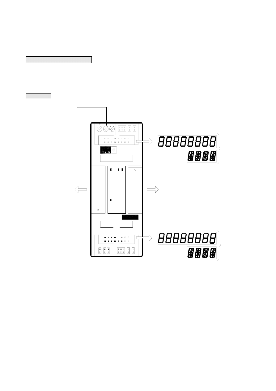
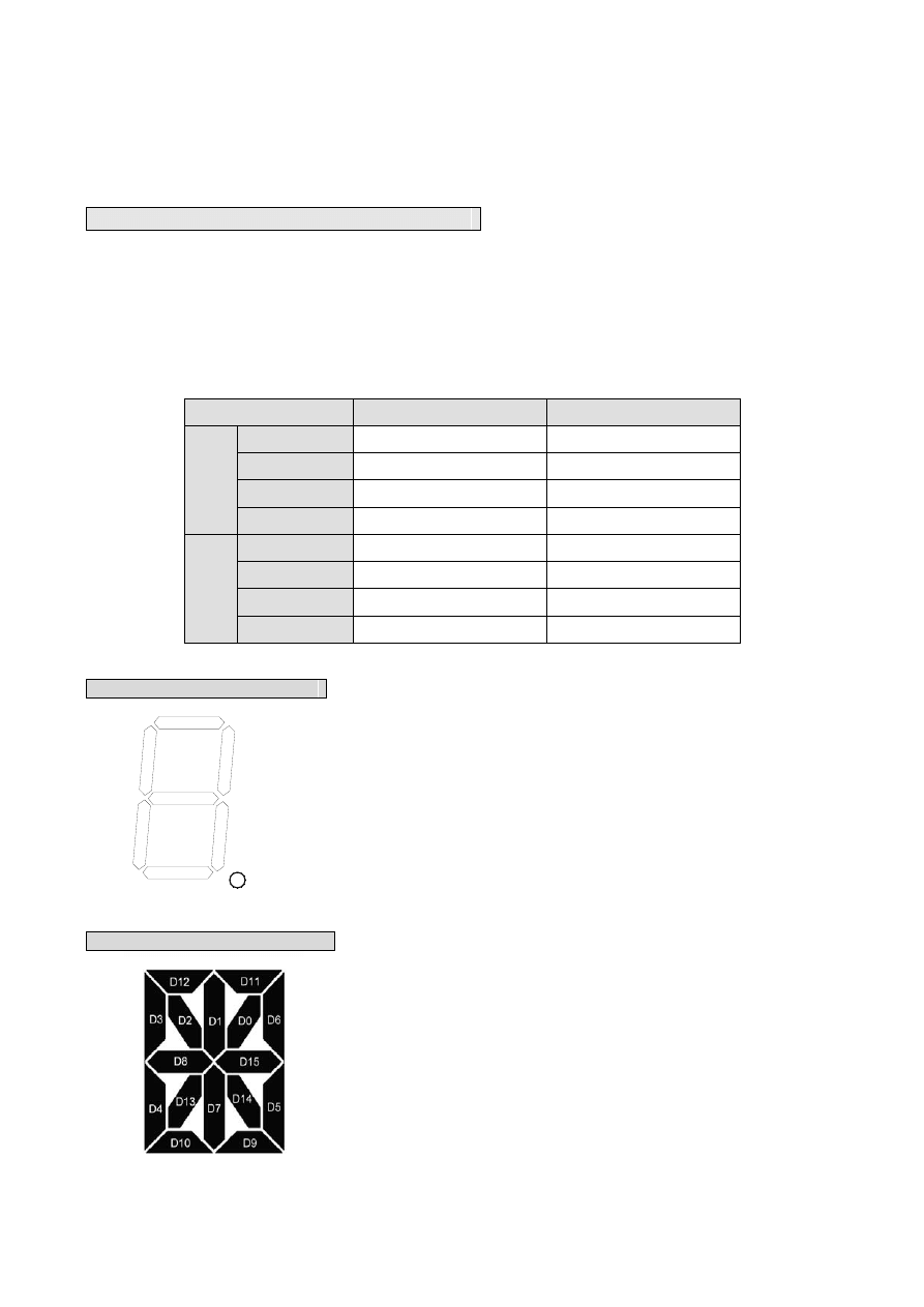
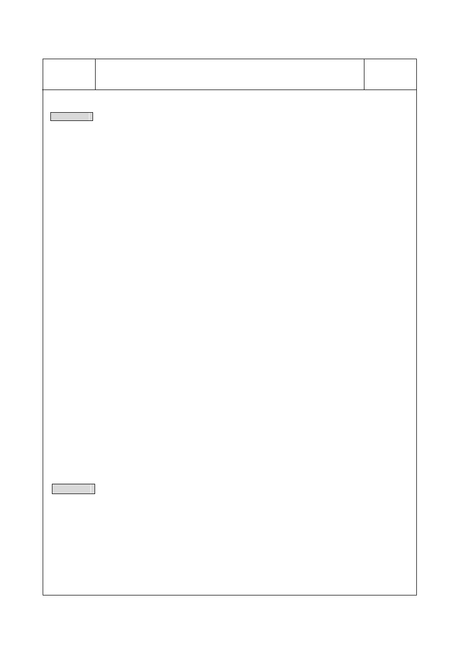
There two models in the FBs-7SG range: 7SG1 and 7SG2. Each of which has one or two 8-digit display driver ICs
for driving eight or sixteen 7-segment LED displays using a common ground; or four or eight 16-segment LED displays.
The drawing below is an example of FBs-7SG2.
Appearance
Expansion input
(connection to main unit or upper
level expansion unit)
FBs-7SG2
CH1
POW
POW
O
V
EXT
O
V
POW
0
CH0
1
External 24V power input
Expansion output
(connect to lower level
expansion unit)
2nd Channel
First Channel
FBs-7SG has been equipped with an exclusive 7-segment LED display driver IC for multiplexing display of one to
eight 7-segment or one to four 16-segment LED displays (one group). With one 16-core flat ribbon cable, users can
display 8 digits (numbers) or 64 independent LED displays (8 LEDs for one digit, selectable between digital or LED
display) or 4-digit character display. Every 7SG module will occupy three to eight output registers(OR) addresses (R3904
~R3967) in the I/O address. Therefore, the PLC can control a maximum of 192 7-segnment displays or 64 16-segment
displays or 1024 independent LED displays.
1 6 - 2
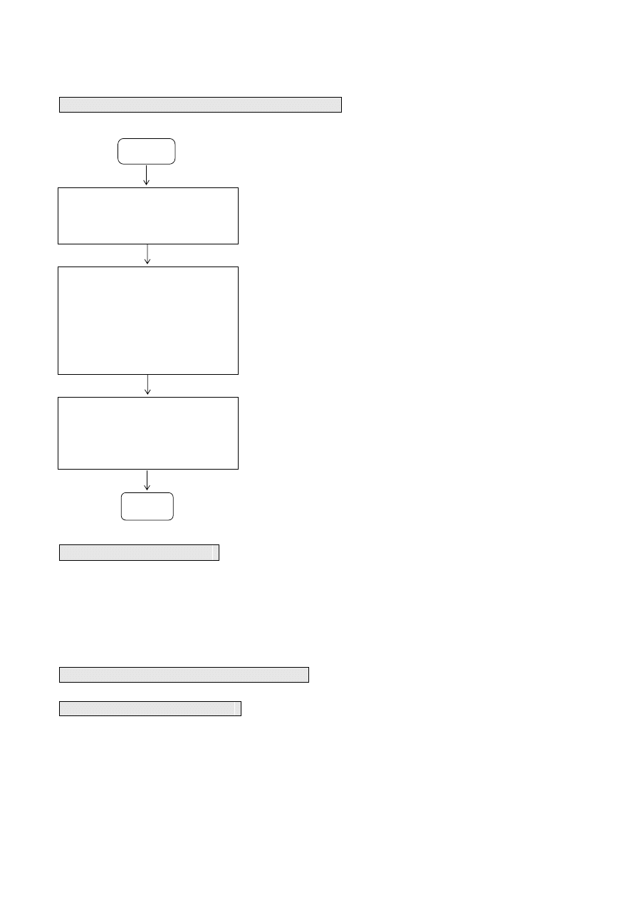
16.2 The Procedure of Using FBs-7SG Module
Start
Install FBs-7SG and connect the
24VDC power cable and 7-segnment
LED display cable.
z See FBs-7SG Hardware Wiring, Section 16.4.1 for details. Refer to
Section 16.4 for details about the circuit of 7-segment LED display
Set appropriate driving voltage for each
group according to the number of LEDs
in each group of the 7-segment display
and adjust LED to the best display
condition according to the forward
voltage drop of each group and ensure
no over voltage (OV) has occurred.
z See FBs-7SG Hardware Setup, Section 16.4.2 for details.
Enter OR to the FBs-PLC to light up the
7-segment LED display or display
characters and numbers by means of
FUN84 (TDSP)
z See FUN84. TDSP Commands, Section 16.8 for details.
End
16.3 FBs-7SG I/O Address
Every FBs-7SG module will occupy three to eight output registers(OR) addresses (R3904~R3967) in the I/O
address. In general, WinProladder will detect and calculate the actual I/O addresses occupied by the expansion modules
installed on the system after connecting to the PLC. Users may refer to the I/O Module Number Configuration provided by
WinProladder in order to find out the exact I/O address of each expansion module to facilitate programming.
16.4 FBs-7SG Hardware Wiring and Setup
16.4.1 FBs-7SG Hardware Wiring
The hardware wiring diagram of FBs-7SG is shown above. In addition to the external 24V power, expansion module
input and expansion module output, users will only need to connect the output to a 7-/16-segment LED display board with
an 16-core FRC flat ribbon cable.
1 6 - 3
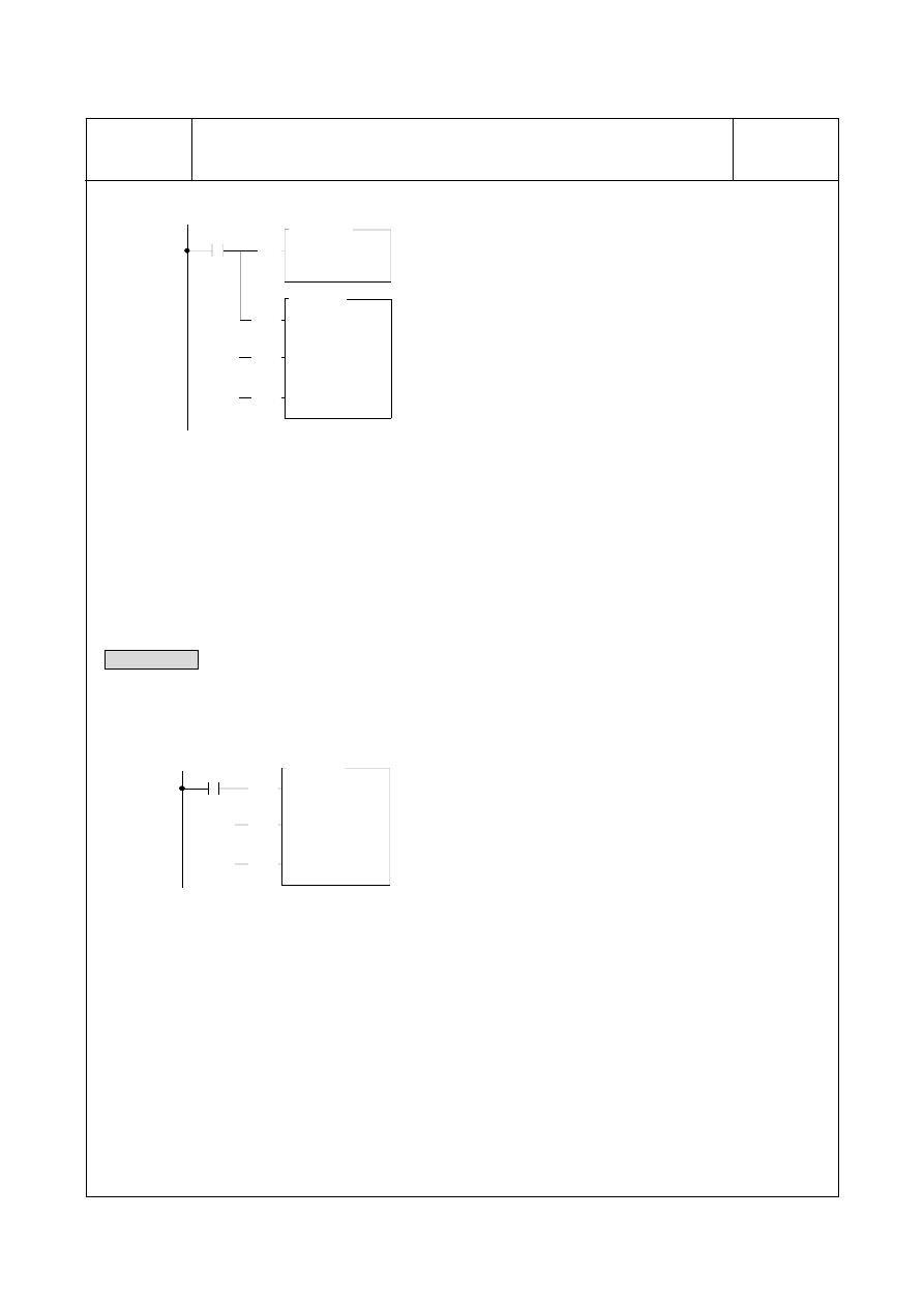
16.4.2 FBs-7SG Hardware Setup
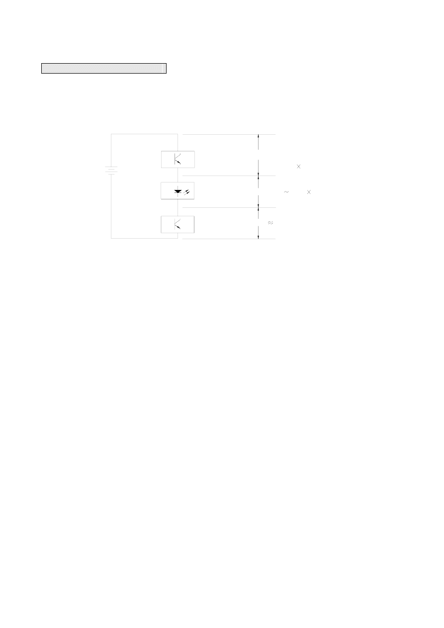
The drawing below presents the output driver circuit of the internal display IC on FBs-7SG. General users will not
need to calculate the voltage drop of LEDs. They will only need to adjust the voltage according to the jumper table below
in order to prevent over voltage.
Driving power source
V
IN
40mA
Fixed current for
displaying IC
7-segment LED
displayer
Multiplexing scan
V
IC
=V
IN
- V
LED
- 0.8V
P
D
=40mA
V
IC
≦ 0.8W
V
LED
=(1.7
2.8V)
Numbers of cascade
connected amp sect LED
V
MUX
0.8V(Fixed)
The power consumption will completely depend on the amount of voltage drop V
IC
(P
D
= 40mA
× V
IC
) connected to it
because the IC current source is fixed at 40mA. As shown in the above diagram, V
IC
= V
IN
− V
LED
− 0.8V, i.e. V
IC
is
affected by the driving current voltage V
IN
and the forward voltage drop of the 7-segment display V
LED
, because the safety
power consumption of display IC at the severest ambient temperature condition must be controlled at or under 0.8W; i.e.
V
IC
must be smaller than 2V. If the V
IC
is too low, the brightness of the LED will be reduced; if it is too high, it will result in
incorrect display (LEDs that are not supposed to be lighted up will be lighted up) or display IC damage.
The forward voltage drop of LED is generally between 1.7V and 2.8V. Depending on the size of ordinary 7-segment
or 16-segment LED displays, each segment (e.g. a-g) consists of one to five LEDs connected in series. While the range
of forward voltage drop among segments will be from 1.7V to 14V, it will be impossible to drive different LED displays with
a single voltage. In order to drive the majority 7-segment LED displays, FBs-7SG comes with four driving voltage options
at 5V (low-voltage), 7.5V, 10V and 12.5V (high voltage for the last three options) and a fine tuning function at 0.6V-1.8V
by means of the diodes and jumpers incorporated to them. In practice, the power supply can drive LEDs of different
forward voltages and prevent display IC from blowing by limiting V
IC
within 2V. The diagrams below show the high/low
voltage setup (common) of LED on FBs-7SG, the high/low voltage driving options of displays and the jumper setting of
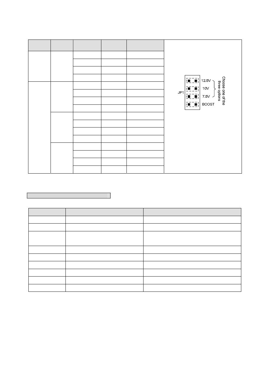
forward voltage drop fine tuning, and its exaction location (as seen after opening the top cover of FBs-7SG).
In this section, we will show you how to obtain the optimal display of 7-/16-segment LED displays without blowing or
shorten the life of the display IC by means of driving voltage (V
IN
) setup, high/low voltage selection and forward voltage
fine tuning.
1 6 - 4
FBs-7SG jumper location
JP5
JP6 .6V
JP7
1V2
JP10
1V2
JP9 .6V
JP3
JP8
D
JP2
JP1
插梢位置圖
(
打開上蓋
)
插梢位置
(
背面
)
HV
LV
HV
LV
T
The jumper settings below are referred to FBs-7SG2, because they have covered those in FBs-7SG1.
Attribute
Jumper Function
Common
JP2
Decode (D closed)/Non-decode (D
open) setting
JP3
O.V. Test (T) or Normal (No Jumper)
setting
JP1
High Voltage (HV) selection (back of
module)
CH0
JP5
High (HV)/Low (LV) voltage selection
JP6
0.6V(0.6V) voltage drop fine tuning
JP7
1.2V(1V2) voltage drop fine tuning
CH1
JP8
High (HV)/Low (LV) voltage selection
JP9
0.6V(0.6V) voltage drop fine tuning
JP10
1.2V(1V2) voltage drop fine tuning
Jumper Layout (open top cover)
Jumper Layout (back of module)
F B s - 7 S G 2
F B s - 7 S G 1
1 6 - 5
JP5/JP8
JP1
JP7/JP10
JP6/JP9
LED Driving
Voltage
Short JP5/JP8 with a jumper
horizontally; place the jumper head onto
the JP5/JP8.
JP1 is located at the back of the module.
Turn module over for setup.
Short only one of the three options
above. JP1 is effective only when HV is
selected from JP5. When LV is selected
from JP5, JP1 will be ineffective.
When BOOST is short, the driving
voltage will be boosted by 5% to
compensate circuit voltage drop. JP5 to
JP7 are effective on CH0 and JP8-JP10
on CH1.
LV Inactive
Open Open
2.4V
Open Short
3V
Short Open
3.6V
Short Short
4.2V
HV
7.5V
Open Open
4.9V
Open Short
5.5V
Short Open
6.1V
Short Short
6.7V
10V
Open Open
7.4V
Open Short
8V
Short Open
8.6V
Short Short
9.2V
12.5V
Open Open
9.9V
Open Short
10.5V
Short Open 11.1V
Short Short 11.7V
FBs-7SG module default jumper setting
Jumper Number Default Jumper Setting
Note
JP1
Locating in third position(7.5V)
Setting as 7.5V mode
JP2
Plugging jumper
Setting as decode mode
JP3
Only plugging in bottom terminal
(equal no Setting)
Don’t do over voltage test(O.V.)
JP5
Locating in LV position
Setting as low voltage mode
JP6
Plugging jumper
Fine tuning 0.6V
JP7
No jumper
JP8
Locating in LV position
Setting as low voltage mode
JP9
Plugging jumper
Fine tuning 0.6V
JP10
No jumper
1 6 - 6
16.4.3 LED Driving Voltage Setup and Over-Voltage (OV) Inspection
Users must select the correct driving voltage according to the voltage requirements of LEDs of different sizes before
applying the module. If the voltage is too low, the brightness of LEDs will be reduced. If the voltage is too high, the
brightness of LEDs will be uneven. More importantly, the LED driver IC will be blown due to over-voltage (O.V.).
Therefore, it is necessary to make sure that the CE intermittent voltage (V
IC
) of the driver IC is below 2V to prevent an
O.V. of the driver IC. Yet, it is difficult for users to measure the V
IC
of driver IC in multiplexing. Therefore, FBs-7SG is
equipped with an O.V. LED indicator to facilitate users to check if an OV occurs. The O.V. indicator is located next to the
output socket on the panel labeled with O.V.
The result of the O.V. indicator is meaningful only when all segments (a total of 64, including the decimal point) are
lighted up. If the O.V. indicator is out in this situation, it means there is no O.V. If the indicator is on, it means there is an
O.V. (the indicator may blink or is on constantly if not all segments are lighted up, in this case, it is meaningless). If you
want to perform a full segment test, set the TEST Jumper (JP3) to “T” (only when the PLC is OFF) on the lower left part of
7SG or use the convenient command (FUN84:TDSP) on 7SG by setting All Input-ON to “1” (PLC is in “RUN” mode) to
light up all segments for an O.V. test.
The following examples show the LED of FBs-7SG module driving voltage setup and O.V. test procedures.
1.
Set JP3 to “T”.
2.
Start with LV and then adjust driving voltage to the required brightness or the O.V. indicator is on according to the
jumper setting as shown in the table above. When the O.V. indicator is on, reduce voltage until the O.V. indicator is
off. Please be noted that if the brightness is at its maximum level but it cannot meet the requirements, replace LEDs
with higher efficiency.
3.
Set JP3 back to ‘N” (normal position) or All Input-ON of FUN84:TDSP to “0”.
Caution
The 7-segment LED display of FBs-7SG is driven by the driver IC with a rated current ≒40mA. The
power consumption depends on the V
IC
of CE because the maximum power limit is only 0.7W/25°C, do
not use module in O.V. condition to prevent the driver IC from blowing.
1 6 - 7
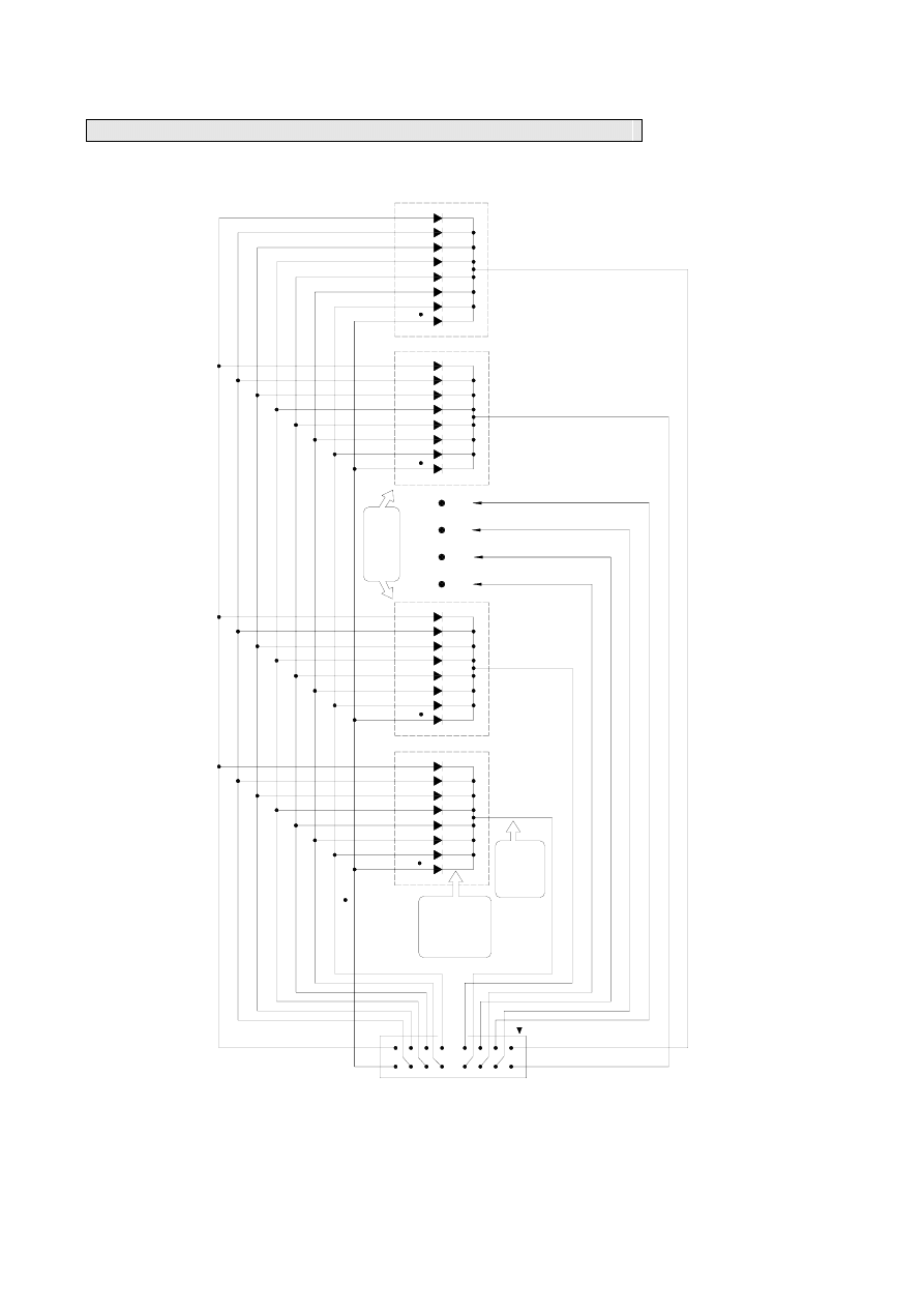
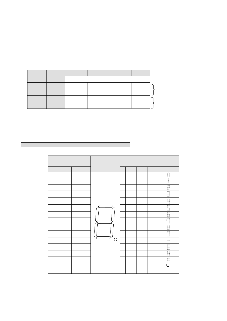
16.5 7-segment LED Display and Individual LED Display Circuits
1
(Le
ast sign
ificant
)
2
3
4
5
6
7
8(
Mo
st signi
fi
ca
nt)
7-s
e
g
m
ent
di
sp
la
y
e
r o
r
In
dep
en
dent
L
E
D
21
3
4
5
6
7
8
10
9
11
12
13
14
15
16
50
49
51
52
53
54
55
56
58
57
59
60
61
62
63
64
15
16
1
2
Ind
e
p
ende
nt
LED
di
sp
la
y
ing
of
n
o
n
-dec
od
in
g
mo
de
Di
gi
t
di
s
p
la
yi
ng
o
f mo
de
d
e
c
odi
ng
b
a
cd
e
f
g
(D0) g
(D1) f
(D2) e
(D
3)
d
(D4)
c
(D5) b
(D6)
a
(D7)
b
a
cd
e
f
g
b
a
cd
e
f
g
b
a
cd
e
f
g
The above diagram indicates the correct wiring (common ground) of the 7-segment LED display or independent
LED display of FBs-7SG. Users may make their own display according to this circuit and layout and connect the display to
any output socket on FBs-7SG with a 16-pin flat ribbon cable. We offer LED display boards and products in six different
dimensions to meet the demands of users. The table below shows the range of our LED display boards and products.
1 6 - 8
Model
Specification
DBAN.8-nR
0.8” 4-digit 16-segment LED display, n means R(Red) 16-segment LED characters
display installed, can be 1~4
DBAN2.3-nR
2.3” 4-digit 16-segment LED display, n means R(Red) 16-segment LED characters
display installed, can be 1~4
DB.56-nR
0.56” 8-digit 7-segment LED display, n means R(Red) 7-segment LED characters
display installed, can be 1~8
DB.8-nR
0.8” 8-digit 7-segment LED display , n means R(Red) 7-segment LED characters
display installed, can be 1~8
DB2.3-nR
2.3” 8-digit 7-segment LED display, n means R(Red) 7-segment LED characters
display installed, can be 1~8
DB4.0-nR
4.0” 4-digit 7-segment LED display , n means R(Red) 7-segment LED characters
display installed, can be 1~4
※ Models inside parentheses are products equipped with LED display and ribbon cable socket.
Recommended pin settings
Model
HV/LV
(JP5/JP8)
JP1
JP7/JP10
JP6/JP9
Driving Voltage
DBAN.8 LV
Open
Short 3V
DBAN2.3 HV
10V
Open Open 7.4V
DB.56
LV
Open
Open
2.4V
DB.8
LV
Short
Open
3.6V
DB2.3
HV
10V
Short
Short
9.2V
DB4.0
HV
10V
Short
Open
8.6V
Users can adjust the pin settings tabulated above table on any FATEK standard products. If higher brightness is
desired, users can fine-tune the driving voltage according to the jumper settings as shown above. Users must avoid over
voltage (O.V.) of output (O.V. indicator will light up) in order not to blow the 7SG module.
Connector pin layout
Pin
Signal
Pin
Signal
1 DIG0 2 DIG1
3 DIG2 4 DIG3
5 DIG4 6 DIG5
7 DIG6 8 DIG7
9 a/D0 10 b/D1
11 c/D2 12 d/D3
13 e/D4 14 f/D5
15 g/D6 16 p/D7
There are two display output connectors on 7SG2, each can support 64 segments of LED display. When all
segments are on, 8 segments will be scanned at a time for a total of 8 times.
1 6 - 9
DIG0-DIG7 as tabulated above refer to low active output signals (Sink or NPN output), only one signal will be active
(multiplexing) at the same time to select a group of LEDs (8 segments). a/D0-p/D7 are source output signals (PNP)
controlling the display of corresponding segments.
16.6 Decode Display and Non-Decode Display
○
1 Non-decode display: (All segments are dimmed, controlled by user-defined applications independently)
A total of 8 ORs are equipped on FBs-7SG2 to control the display of 128 segments. Each segment is controlled by a
corresponding bit. When the bit value is 1, the corresponding segment will light up. The correlations of each segment and
OR is tabulated below. OR is the first output register that occupied by the module. Each OR will output signals twice, i.e. 1
bit of data (8 segments) each time. These data will be transferred to the corresponding outputs p/D7-a/D0.
OR
D15~D8
D7~D0
CH0
OR+0
SEG15~SEG8 SEG7~SEG0
OR+1
SEG31~SEG24 SEG23~SEG16
OR+2
SEG47~SEG40 SEG39~SEG32
OR+3
SEG63~SEG56 SEG63~SEG48
CH1
OR+4
SEG15~SEG8 SEG7~SEG0
OR+5
SEG31~SEG24 SEG23~SEG16
OR+6
SEG47~SEG40 SEG39~SEG32
OR+7
SEG63~SEG56 SEG63~SEG48
7-segment LED correspondence
D6
D1
D2
D5
D4
D3
D7
D0
a
f
b
e
c
d
g
P
16-segment LED correspondence
The digit on the farthest right of the display board (8 digits, max.)
corresponds to outputs SEG0-SEG7; the next digit to the left corresponds to
outputs SEG8-SEG15; the digit on the farthest left of the display board
corresponds to outputs SEG63-SEG56. Each 7SG2 can drive sixteen
7-segment LED displays.
Segments D0-D15 of the digit on the farthest right of the display board (4
digits, max.) correspond to outputs SEG0-SEG15 on 7SG2; the next digit to
the left corresponds to outputs SEG16-SEG31; the digit on the farthest left of
the display board corresponds to outputs SEG63-SEG48. Each 7SG2 can
drive 8 16-segment LED displays.
1 6 - 1 0
○
2
Decode Display : Display data on the corresponding segments with default coding
In this mode, a total of 4 output registers(OR) are equipped on FBs-7SG2 to control the display of 8 digits of
7-segment LEDs. Each digit is controlled by 4 bits. The decimal point of an 8-digit number is controlled by the first output
register. Each point is controlled by the corresponding bit. The correlations among the digits, decimal point and ORs are
tabulated below. OR is the first output register that occupied by the module.
Attribute
OR
D15~D12
D11~D8
D7~D4
D3~D0
Common
OR+0
P15~P8
P7~P0
CH0
OR+1
DIG3
DIG2
DIG1
DIG0
OR+2
DIG7
DIG6
DIG5
DIG4
CH1
OR+3
DIG3
DIG2
DIG1
DIG0
OR+4
DIG7
DIG6
DIG5
DIG4
OR0 controls the display of decimal point. When the value is “1”, the corresponding decimal point will light up.
OR1-OR4 control the display of 16-digit numbers. Each digit will be controlled by four corresponding bits. A total of 16
changes correspond to the following displays.
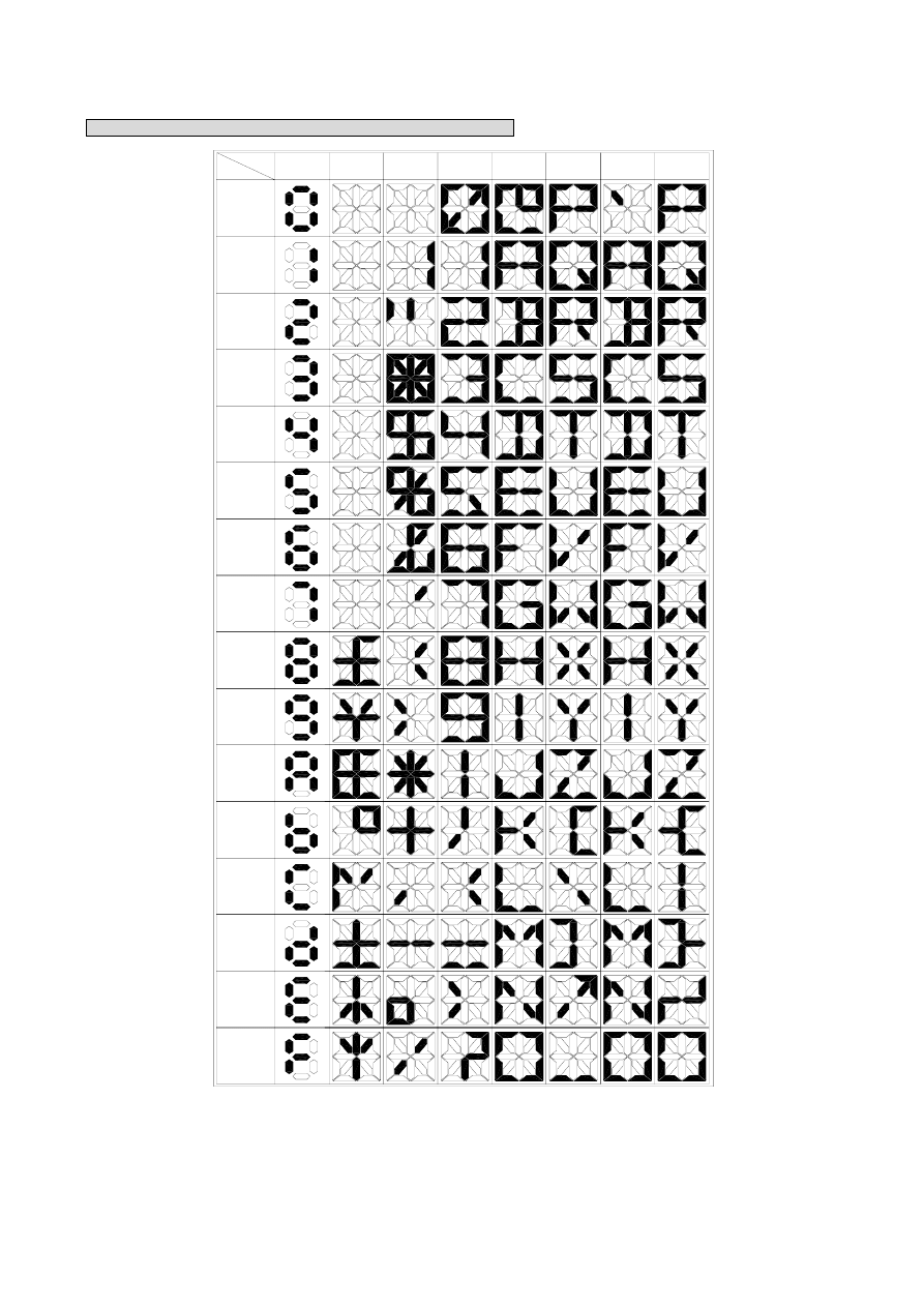
4-bit digital 7-segment LED decode and non-decode number displays
Nibble Value
7-segment LED
display structure
Segment DIM (0)
ON (1)
Number
Hexadecimal
Binary
a
b
c
d
e
f
g
0 0000
g
b
a
f
e
d
c
P
1
1
1
1
1
1
0
1 0001
0
1
1
0
0
0
0
2 0010
1
1
0
1
1
0
1
3 0011
1
1
1
1
0
0
1
4 0100
0
1
1
0
0
1
1
5 0101
1
0
1
1
0
1
1
6 0110
1
0
1
1
1
1
1
7 0111
1
1
1
0
0
1
0
8 1000
1
1
1
1
1
1
1
9 1001
1
1
1
1
0
1
1
A
1010
0
0
0
0
0
0
1
B
1011
1
0
0
1
1
1
1
C
1100
0
1
1
0
1
1
1
D
1101
0
0
0
1
1
0
1
E
1110
0
0
0
1
1
1
1
F
1111
0
0
0
0
0
0
0
1_st 8-digit
2_nd 8-digit
1 6 - 11
ASCII Code and 16-segment number display cross-reference table
x 1 1 0
x 1 1 1
x 0 0 0
x 0 0 1
x 0 1 0
x 0 1 1
x 1 0 0
x 1 0 1
0 0 0 0
0 0 0 1
0 0 1 0
0 0 1 1
0 1 0 0
0 1 0 1
0 1 1 0
0 1 1 1
1 0 0 0
1 0 0 1
1 0 1 0
1 0 1 1
1 1 0 0
1 1 0 1
1 1 1 0
1 1 1 1
M S B
L S B
1 6 - 1 2
16.7 FBs-7SG Input Power Requirements and Consumption
FBs-7SG is equipped with a DC24V isolated power supply to convert an external 24V power input into power supply
for use by the internal circuit and 7-segment LED display on FBs-7SG. The tolerance of input is DC24V
±20%.
FBs-7SG consumes 2Wmax when idled. The consumption increases according to the number of 7-segments lighted
up. The segment driving current of every display IC on FBs-7SG is 40mA. The driving current for displaying one digit
using 8 segments consumes 320mA, and the maximum power consumption of a group is obtained as formulated below:
Pd = 320mA
× V
IN
(LED driving voltage) ÷ 0.8 (power efficiency) W
Total consumption = 2 + Pd
× n(W)
For example, the total power consumption of FBs-7SG2 (output from both groups) at maximum power (V
IN
= 12.5V,
all 8 segments are on):
2W +(320mA
× 12.5V ÷8 )= 7W
16.8 Controlling Display Contents with OR on FBs-7SG
There are two ways to light up an LED with FBs-7SG. In this section, we will introduce the method of how to light up
a 7-segment number display by programming the OR output. In the next section, we will continue with displaying special
symbols with FUN84. If displaying numbers with OR controls in decode mode, digits in front of a number will be displayed
as 0.
If expansion modules are connected to the FBs PLC, these modules and the I/O address they occupied (see
Chapter 12, WinProladder User’s Manual for details) will be displayed on the screen when WinProladder is connected to
the PLC. If a FBs-7SG2 is connected to the FBs PLC, users will find in the project window that the system has
automatically assigned the output address to FBs-7SG2 when WinProladder is connected to the PLC.
Program example 1 (Decode Display Mode)
Control of 8-digit 7-segment display with FBs-7SG1, with decimal point on. In this case, the FBs-7SG1 must be set
to Decode Mode.
EN
D :
S :
EN
S :
D :
D :
EN
S :
M0
08.MOV
08.MOV
08.MOV
00FFH
R3904
5678H
1234H
R3906
R3905
1 6 - 1 3
Description :
When M0=1, move the value to be output to the OR. As described above, OR+0 (R3904 in the example) controls
the display of decimal point in decode mode; OR+1 (R3905 in the example) controls the display of the lower section of the
four digits and OR+2 (R3906 in the example) the upper section of the four digits. The results are:
OR
Contents
R3904
00FFH
R3905
5678H
R3906
1234H
Program example 2 (Non-decode Display Mode)
Display numbers on the 8-digit 7-segment display with FBs-7SG1, with decimal point on. In this case, the FBs-7SG1
must be set to Non-decode Mode.
M0
EN
R3904
D :
08.MOV
S :
D :
EN
S :
R3905
08.MOV
08.MOV
R3906
D :
S :
EN
EN
08.MOV
D :
S :
EDB0H
B3F9H
R3907
DFDBH
CFBDH
Description :
When M0=1, move the value to be output to the OR. As described above, OR+0 (R3904 in the example) controls
the display of the first two digits, OR+1 (R3905 in the example) the third and fourth digits, OR+2 (R3906 in the example)
the fifth and sixth digits, and OR+3(R3907 in the example) the last two digits. The results are:
OR
Contents
R3904
EDB0H
R3905
B3F9H
R3906
DFDBH
R3907
CFBDH
16.9 FBs-7SG Output Commands FUN84: TDSP
The TDSP commands are described in the next page.
7-segment display contents :
1.2.3.4.5.6.7.8.
7-segment display contents :
E.d.6.5.4.3.2.1.
TDSP
16-14
FUN84
TDSP
FBs-7SG Display Module Convenient Commands
7/16-segment display character and number display conversion
FUN84
TDSP
Md : Operation Mode, 0~3
S : Starting address of being converted characters
Ns : Start of source character, 0~63
Nl : Length of character, 1~64
D : Starting address to store the converted pattern
Nd : Start pointer while storing
S operand can be combined with V、Z、P0~P9
index registers for indirect addressing
Range
Oper
-and
HR
OR
ROR
DR
K
Index
R0
∣
R3839
R3904
∣
R3967
R5000
∣
R8071
D0
∣
D3999
Positive
integer
16/32-bit
V 、 Z 、
P 0 ~ P 9
Md
0 ~ 3
S
○
○
○
○
○
Ns
○
○
○
○
0 ~ 6 3
Nl
○
○
○
○
1 ~ 6 4
D
○
○
○*
○
Nd
○
○
○*
○
0 ~ 6 3
●
This convenient instruction is used to generate the corresponding display pattern for FBs series 7-segment or
16-segment display pannel under the control of FBs-7SG1 or FBs-7SG2 modules.
When execution control "EN"=1, input "OFF"=0, and input "ON"= 0, this instruction will perform the display
pattern conversion, where S is the starting address storing the being converted characters, Ns is the pointer
to locate the starting character, Nl tells the length of being converted characters, and D is the starting address
to store the converted result, Nd is the pointer to locate the start of storing.
There are 4 kinds of operation mode as below:
Md=0, display pattern conversion for 16-segment display; the source character is the
8-bit ASCII Code, the converted result is the 16-bit display pattern. By the
control of M1990, it determines the display direction, where
M1990=0, right to left display ; M1990=1, left to right display
Md=1, Without leading zero display conversion for 16-segment display; the source
character is the 8-bit ASCII Code, the converted result is the 16-bit display
pattern without leading zero.
Md=2, Non-decoded display pattern conversion for 7-segment display; the source
character is the 4-bit nibble code, the converted result is the 8-bit display pattern.
Md=3, Without leading zero display conversion for 7-segment decoded display; the
source character is the 4-bit nibble code, the converted result is the 4-bit display
pattern without leading zero.
Byte 0 or Nibble 0 of S is the 1
st
displaying character, Byte 1 or Nibble 1 of S is the 2
nd
displaying character,…
Ns operand is the pointer to tell where the displaying character starts
Nl operand is the character quantity for conversion
TDSP
16-15
FUN84
TDSP
FBs-7SG Display Module Convenient Commands
7/16-segment display character and number display conversion
FUN84
TDSP
D operand is the starting address to store the converted display pattern; while Md=0 or 1, one source
character of 8-bit ASCII code needs one 16-bit location to store the result; while Md=2, one source character
of 4-bit nibble code needs one 8-bit location to store it; while Md=3, one source character of 4-bit nibble code
needs one 4-bit location to store it.
Nd operand is the pointer to tell where is the start to store the converted pattern.
●
When inputs "OFF"=1, "ON"=0, and "EN"=0/1, the D operand will be filled with the all OFF pattern according
to the operation mode, the Nd pointer, and the quantity of Nl.
●
When inputs "ON"=1, "OFF"=0/1, and "EN"=0/1, the D operand will be filled with the all ON pattern according
to the operation mode, the Nd pointer, and the quantity of Nl.
●
Data will be converted differently based on the selected mode. The description below is based on Example 2.
In Example 2, MD=1; S=R0; Ns=0; Nl=8; D=R3904; and Nd=8. Data conversion is presented below.
Example1
8-character of text display by using the FBs-7SG2 display module and 16-Segment display panels; for this
application, the FBs-7SG2 module must be set to work at the non-decoded operation mode.
The WinProladder supports the "ASCII Table" editing for easy and convenient text message display; we
can create one ASCII Table with the content ' WELCOME ' for testing, and we assign R5000 is the table
starting address, then R5000~R5007 will have the following contents :
TDSP
16-16
FUN84
TDSP
FBs-7SG Display Module Convenient Commands
7/16-segment display character and number display conversion
FUN84
TDSP
R5000=2027H (20H= ; 27H=')
R5001=4557H (45H=E ; 57H=W)
R5002=434CH (43H=C ; 4CH=L)
R5003=4D4FH (4DH=M; 4FH=O)
R5004=2045H (20H= ; 45H=E)
R5005=2C27H (2CH=,; 27H=')
R5006=4E45H (4EH=N ; 45H=E)
R5007=0044H (00H= ; 44H=D)
M1990
R5000
2
84.TDSP
MD:
M100
EN
N
S
:
Nl :
0
S500
S :
D :
Nd:
R3904
OFF
M101
ON
M102
8
0
Description: When M100=1, M101=0 and M102=0, the FUN84 will perform the display pattern conversion, where
the source (S) begins from the R5000, the start pointer (Ns) is pointed to byte 2, and the quantity
(Nl) is 8, it means the contents of R5001~R5004 are the displaying characters; the registers
R3904~R3911 will store the converted pattern for text message displaying (D operand begins from
R3904, Nd operand is pointed to word 0, Nl operand is 8 for quantity)
While M1990=1, the 16-segment panel will display "WELCOME " ;
While M1990=0, the 16-segment panel will display " EMOCLEW".
When M101=1, M102=0, the registers R3904~R3911 will be filled with the all OFF pattern for
displaying.
When M102=1, the registers R3904~R3911 will be filled with the all ON pattern for displaying.
Example2
8-character of display without the leading zero through the second FBs-7SG2 display module and
16-Segment display panels; for this application, the FBs-7SG2 module must be set to work at the non-decoded
operation mode.
R0
0
84.TDSP
MD:
M110
EN
N
S
:
Nl :
1
S :
D :
Nd:
R3904
OFF
ON
8
8
TDSP
16-17
FUN84
TDSP
FBs-7SG Display Module Convenient Commands
7/16-segment display character and number display conversion
FUN84
TDSP
Description
When M110=1, the FUN84 will perform the display pattern conversion, where the source (S) begins from
the R0, the start pointer (Ns) is pointed to byte 0, and the quantity (Nl) is 8, it means the contents of R0~
R3 are the displaying characters; the registers R3912~R3919 will store the converted pattern for
message displaying (D operand begins from R3904, Nd operand is pointed to word 8, Nl operand is 8 for
quantity).
(1) R0=0008H
R1=0506H
R2=0304H
R3=0102H
Display on the 16-segment display :
"12345608"
(2) R0=0708H
R1=0506H
R2=0000H
R3=0000H
Display on the 16-segment display :
" 5678"
(3) R0=3738H
R1=3536H
R2=3334H
R3=3132H
Display on the 16-segment display :
"
12345678
"
(4) R0=3038H
R1=3536H
R2=3334H
R3=3030H
Display on the 16-segment display :
"
345608
"
※
The I/O address of FBs-7SG2 in Example 2 must be at R3912~R3919 to ensure the correct display of the
message/number (length=8); i.e. other digital or analog output modules may be connected in front of FBs-7SG2.
Example3
4-digit of numeric display and 32-point of external independent LED's display through the control of
FBs-7SG1 display module and 4-digit of 7-segment display panel; also, it needs the extra circuit to control the
32-point of independent LED's display. For this application, the FBs-7SG1 module must be set to work at the
non-decoded operation mode.
TDSP
16-18
FUN84
TDSP
FBs-7SG Display Module Convenient Commands
7/16-segment display character and number display conversion
FUN84
TDSP
R 0
0
84.TD S P
M D :
E N
N
S
:
N l :
2
4
S :
D :
N d:
0
R 3906
O FF
O N
08D .M O V
E N
D :
R 3904
S :
M 120
W M 0
Description : When M120=1, the status of M0~M31 will be copied to the output registers R3904~R3905 to
control the display of the 32-point of independent LEDs. The FUN84 also performs the display
pattern conversion, where the source (S) begins from the R0, the start pointer (Ns) is pointed to
nibble 0, and the quantity (Nl) is 4, it means nibble0~nibble3 of R0 are the displaying characters;
the output registers R3906~R3907 will store the converted pattern for displaying (D operand
begins from R3906, Nd operand is pointed to byte 0, Nl operand is 4 for quantity).
R0=1024H Æ The 7-segment panel will display "1024"
Example 4
12-digit of decoded numeric display without the leading zero through the control of FBs-7SG2 display
module and 12-digit of 7-segment display panels. For this application, the FBs-7SG2 module must be set to work
at the decoded operation mode.
R 0
0
8 4 .T D S P
M D :
E N
N
S
:
N l :
S :
D :
N d :
O F F
O N
M 1 3 0
3
R 3 9 0 5
1 2
0
Description:When M130=1, the FUN84 will perform the display pattern conversion, where the source
(S) begins from the R0, the start pointer (Ns) is pointed to nibble 0, and the quantity (Nl) is 12, it
means nibble0~nibble11 of R0~R2 are the displaying characters; the output registers R3905~
R3907 will store the converted pattern for displaying (D operand begins from R3904, Nd operand is
pointed to nibble 0, Nl operand is 12 for quantity).
(1).
R2=1234H, R1=5678H, R0=9000H
Display on the 7-segment display : "123456789000"
(2).
R2=0000H, R1=5678H, R0=9000H
Display on the 7-segment display : " 56789000"
Wyszukiwarka
Podobne podstrony:
Figures for chapter 16
Exploring Economics 3e Chapter 16
Innovative Inventory and Production Management Techniques Chapter 16
Fundamentals of College Physics Chapter 16
English Skills with Readings 5e Chapter 16
Environmental Science 12e Chapter 16
chapter 16 defAssign
Phonetics and Phonology 16 10 13 Gimson Chapter 2 Produ
Fundamentals of Anatomy and Physiology 16 Chapter
Sld 16 Predykcja
Ubytki,niepr,poch poł(16 01 2008)
Figures for chapter 5
Figures for chapter 12
16 Metody fotodetekcji Detektory światła systematyka
Figures for chapter 6
wyklad badania mediow 15 i 16
RM 16
więcej podobnych podstron