7
9
25274 75349
0 9>
CIRCUIT
CELLAR
®
www.circuitcellar.com
T H E M A G A Z I N E F O R C O M P U T E R A P P L I C AT I O N S
$4.95 U.S. ($5.95 Canada)
#170 September 2004
SIGNAL PROCESSING
Multipurpose Test Instrument
MCU-Based Lamp Controller
USB-to-DMX-512 Converter
Four-Port USB Hub
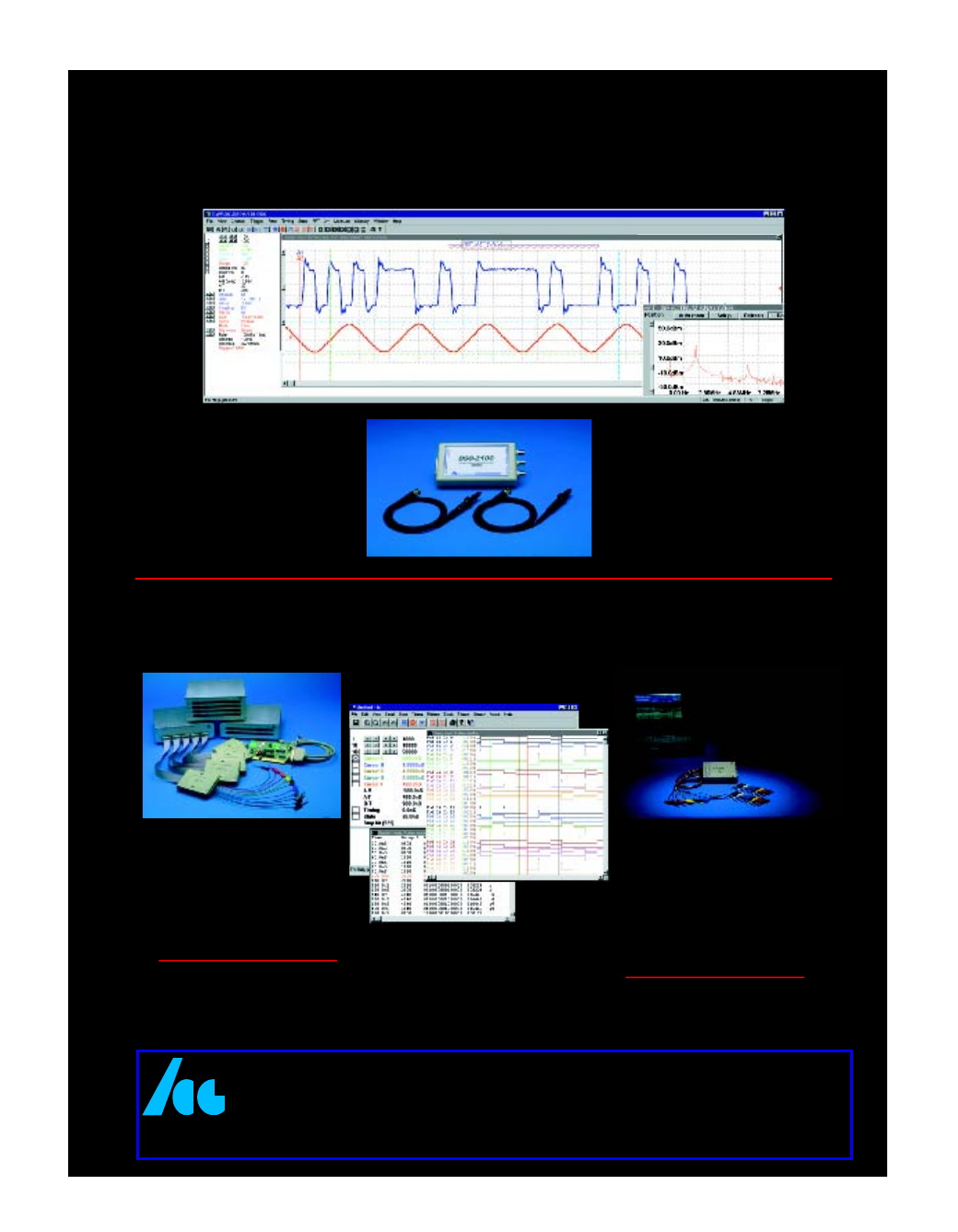
Digital Oscilloscopes
•
2 Channel Digital Oscilloscope
•
100 MSa/s
max single shot rate
•
32K samples per channel
•
Advanced Triggering
•
Only 9 oz and 6.3” x 3.75” x 1.25”
•
Small, Lightweight, and Portable
•
Parallel Port
interface to PC
•
Advanced Math options
•
FFT Spectrum Analyzer options
DSO-2102S
$525
DSO-2102M
$650
Each includes
Oscilloscope
,
Probes, Interface Cable, Power
Adapter, and software for
Win95/98, WinNT, Win2000
and DOS.
•
40 to 160 channels
•
up to 500 MSa/s
•
Variable Threshold
•
8 External Clocks
•
16 Level Triggering
•
up to 512K samples/ch
•
Optional Parallel Interface
•
Optional 100 MSa/s Pattern Generator
LA4240-32K (200MHz, 40CH)
$1350
LA4280-32K (200MHz, 80CH)
$2000
LA4540-128K (500MHz, 40CH)
$1900
LA4580-128K (500MHz, 80CH)
$2800
LA45160-128K (500MHz, 160CH)
$7000
Logic Analyzers
• 24 Channel Logic Analyzer
• 100MSa/S max sample rate
• Variable Threshold Voltage
• Large 128k Buffer
• Small, Lightweight and Portable
• Only 4 oz and 4.75” x 2.75” x 1”
• Parallel Port Interface to PC
• Trigger Out
• Windows 95/98 Software
LA2124-128K (100MSa/s, 24CH)
Clips, Wires, Interface Cable, AC
Adapter and Software
$800
All prices include Pods and Software

I
n our past reader surveys, many of you have said you hold onto our old
issues. This Signal Processing issue will make a great addition to your ref-
erence library. We have an impressive lineup of articles this month featur-
ing a wide range of applications.
In “The Engineer’s Alarm Clock: Design a PIC-Based Lamp Controller,”
Aaron Dahlen describes the first of two innovative lamp controller projects
in this issue (p. 18). Aaron built a lamp controller that gradually brightens a
120-VAC incandescent light bulb. This unique Microchip PIC18F252-based
system simulates the natural sunrise, which Aaron finds particularly helpful on
dark winter mornings. For convenience, he designed the system to be con-
trolled remotely. Furthermore, using an infrared remote control enabled
him to simplify the user interface, making this project a snap to build.
Stefan Kalbermatter designed an effective lighting control system using
the FT232BM USB-to-serial converter chip from Future Technology
Devices International (p. 72). With the FT232BM, Stefan was able to build
an inexpensive USB-to-DMX-512 converter that enables him to work from
his laptop. The mobile system can control eight 230-V, 2-kW channels con-
nected to halogen floodlights. In this article, Stefan covers the basics of the
DMX-512 protocol and walks us through his design process.
On page 54, you’ll find another useful laptop project. Using Texas
Instruments components, columnist Jeff Bachiochi built a four-port hub
designed to enhance the productivity of his laptop that has just one USB
port. This power-saving system enables him to connect a printer, digital
camera, or joystick in addition to the mouse he ordinarily uses.
Brian Millier takes us out of the field and into the lab. If you’ve been won-
dering what your workbench has been missing, look no further than the
Zilog Z8 Encore!-based Multilab. Brian’s latest design combines an arbi-
trary function generator, a digital pulse generator, a high-resolution DC
voltmeter, and a DC reference source to create an extremely useful multi-
purpose piece of test equipment (p. 46). He used a PDA for control so that
he could minimize the size and cost of the instrument.
Cutting cost is an essential part of most of the projects that we feature,
including the sound-effect system developed by Praveen Deshpande and
Prajakta Deshpande (p. 62). Their Intel MCS-51 microcontroller-based
system generates musical sounds for the digital clock they designed. After
you’ve read this thorough article, you’ll be ready to make your own micro-
controller-driven sound effects.
I also wanted to draw your attention to one other excellent project we have
this month. While designing a variable frequency drive to control three-phase
AC motors, Armando Rosas Morato and Sergio Elizarraras Rodriguez devel-
oped a scheme for unipolar sine wave pulse-width modulation (p. 32). In their
article, “An SPWM Calculator: Using the Switched Integration Technique,”
they discuss their high-performance quadrature SPWM modulation tech-
nique, or QUSPWM. The QUSPWM algorithm, written in MATLAB by
MathWorks, is an effective tool for analysis.
I regret to report that Sergio lost his battle with cancer six weeks before
this article was published. All of us here at Circuit Cellar send our condo-
lences to Armando, his coauthor and friend.
4
Issue 170 September 2004
www.circuitcellar.com
CIRCUIT CELLAR
®
EDITORIAL DIRECTOR/FOUNDER
Steve Ciarcia
MANAGING EDITOR
Jennifer Huber
TECHNICAL EDITOR
C.J. Abate
WEST COAST EDITOR
Tom Cantrell
CONTRIBUTING EDITORS
Ingo Cyliax
Fred Eady
George Martin
George Novacek
Jeff Bachiochi
NEW PRODUCTS EDITOR
John Gorsky
PROJECT EDITORS
Steve Bedford
Ken Davidson
David Tweed
ADVERTISING
PUBLISHER
Dan Rodrigues
E-mail: dan@circuitcellar.com
ASSOCIATE PUBLISHER/DIRECTOR OF SALES
Sean Donnelly
Fax: (860) 871-0411
(860) 872-3064
E-mail: sean@circuitcellar.com
Cell phone: (860) 930-4326
ADVERTISING COORDINATOR
Valerie Luster
Fax: (860) 871-0411
(860) 875-2199
E-mail: val.luster@circuitcellar.com
ADVERTISING ASSISTANT
Deborah Lavoie
Fax: (860) 871-0411
(860) 875-2199
E-mail: debbie.lavoie@circuitcellar.com
CONTACTING CIRCUIT CELLAR
SUBSCRIPTIONS:
INFORMATION: www.circuitcellar.com or subscribe@circuitcellar.com
To Subscribe: (800) 269-6301, www.circuitcellar.com/subscribe.htm, or
subscribe@circuitcellar.com
PROBLEMS: subscribe@circuitcellar.com
GENERAL INFORMATION:
TELEPHONE: (860) 875-2199 Fax: (860) 871-0411
INTERNET: info@circuitcellar.com, editor@circuitcellar.com, or www.circuitcellar.com
EDITORIAL OFFICES: Editor, Circuit Cellar, 4 Park St., Vernon, CT 06066
NEW PRODUCTS: New Products, Circuit Cellar, 4 Park St., Vernon, CT 06066
newproducts@circuitcellar.com
AUTHOR CONTACT:
E-MAIL: Author addresses (when available) are included at the end of each article
CIRCUIT CELLAR®, THE MAGAZINE FOR COMPUTER APPLICATIONS (ISSN 1528-0608) and Circuit Cellar Online are pub-
lished monthly by Circuit Cellar Incorporated, 4 Park Street, Suite 20, Vernon, CT 06066 (860) 875-2751. Periodical rates paid at
Vernon, CT and additional offices. One-year (12 issues) subscription rate USA and possessions $21.95, Canada/Mexico
$31.95, all other countries $49.95. Two-year (24 issues) subscription rate USA and possessions $39.95, Canada/Mexico
$55, all other countries $85. All subscription orders payable in U.S. funds only via VISA, MasterCard, international postal money
order, or check drawn on U.S. bank.
Direct subscription orders and subscription-related questions to Circuit Cellar Subscriptions, P.O. Box 5650, Hanover, NH
03755-5650 or call (800) 269-6301.
Postmaster: Send address changes to Circuit Cellar, Circulation Dept., P.O. Box 5650, Hanover, NH 03755-5650.
For information on authorized reprints of articles,
contact Jeannette Ciarcia (860) 875-2199 or e-mail jciarcia@circuitcellar.com.
Circuit Cellar® makes no warranties and assumes no responsibility or liability of any kind for errors in these programs or schematics or for the
consequences of any such errors. Furthermore, because of possible variation in the quality and condition of materials and workmanship of read-
er-assembled projects, Circuit Cellar® disclaims any responsibility for the safe and proper function of reader-assembled projects based upon or
from plans, descriptions, or information published by Circuit Cellar®.
The information provided by Circuit Cellar® is for educational purposes. Circuit Cellar® makes no claims or warrants that readers have a right to
build things based upon these ideas under patent or other relevant intellectual property law in their jurisdiction, or that readers have a right to
construct or operate any of the devices described herein under the relevant patent or other intellectual property law of the reader’s jurisdiction.
The reader assumes any risk of infringement liability for constructing or operating such devices.
Entire contents copyright © 2004 by Circuit Cellar Incorporated. All rights reserved. Circuit Cellar and Circuit Cellar INK are registered trademarks
of Circuit Cellar Inc. Reproduction of this publication in whole or in part without written consent from Circuit Cellar Inc. is prohibited.
CHIEF FINANCIAL OFFICER
Jeannette Ciarcia
CUSTOMER SERVICE
Elaine Johnston
CONTROLLER
Jeff Yanco
ART DIRECTOR
KC Prescott
GRAPHIC DESIGNER
Mary Turek
STAFF ENGINEER
John Gorsky
QUIZ COORDINATOR
David Tweed
Cover photograph Chris Rakoczy—Rakoczy Photography
PRINTED IN THE UNITED STATES
One for the Library
jennifer.huber@circuitcellar.com
TASK MANAGER


6
Issue 170 September 2004
CIRCUIT CELLAR
®
www.circuitcellar.com
September 2004: Signal Processing
TASK MANAGER
One for the Library
FEATURES
COLUMNS
DEPARTMENTS
PRIORITY INTERRUPT
The Most Success Yet
Design a PIC-Based Lamp Controller
Aaron Dahlen
Using the Switched Integration Technique
Armando Rosas Morato & Sergio Elizarraras Rodriguez
Build a Z8 Encore!-Based Multipurpose Test Instrument
Brian Millier
Microcontroller-Driven Sound Effects
Praveen Deshpande & Prajakta Deshpande
Build a USB-to-DMX-512 Converter
Stefan Kalbermatter
PIC18F252-Based Alarm System (p. 18)
USB-to-DMX-512 Converter (p. 72)
8
Issue 170 September 2004
CIRCUIT CELLAR
®
www.circuitcellar.com
NEW PRODUCT NEWS
Edited by John Gorsky
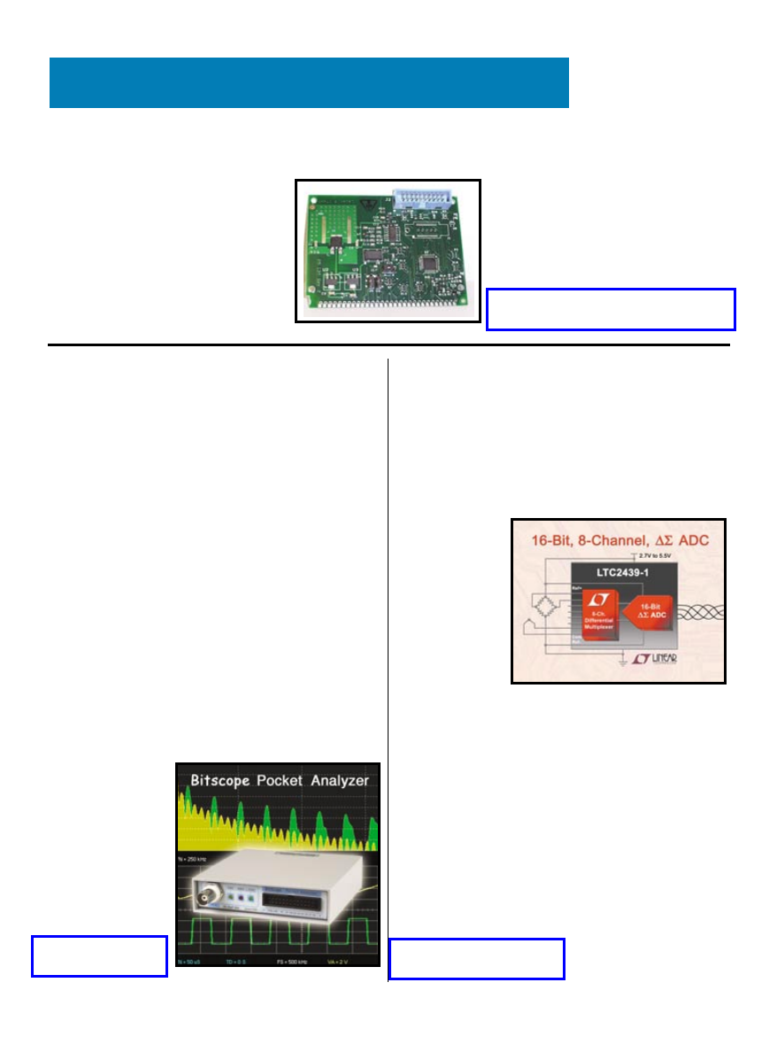
USB OSCILLOSCOPE AND LOGIC ANALYZER
Based on an original design published in Circuit Cellar
issue 97 (August 1998), the Pocket Analyzer is the newest
member of the growing BitScope family.
Like all BitScopes, the Pocket Analyzer combines a high
bandwidth digital storage oscilloscope with a fast sample-
synchronized logic analyzer. However, this new BitScope is
unique in that it offers an integrated analog waveform and
logic pattern generator and a BitScope “Smart POD” con-
nector in a tiny USB-powered package. Roughly the size
of a Pocket PC and requiring no bulky accessories, the
BitScope Pocket Analyzer is the ideal go-anywhere test-
and-debug solution.
The Pocket Analyzer operates with BitScope’s standard
DSO software (available for Windows and Linux) to give
you an array of integrated “virtual instruments,” including
standard oscilloscope and logic analyzer functions, a spec-
trum analyzer, X-Y phase plotter, and waveform/logic pat-
tern generators.
A connection to your circuit is made via a set of mini-
clip test leads that plug directly into the Smart POD con-
nector. In addition to the eight logic signals, two analog
inputs are also available on the POD to support dual-chan-
nel oscilloscope operation.
A third analog input is available via the BNC connector,
which allows for the use of standard oscilloscope probes.
With its built-in ×10
input prescaler and a
×1/×10 probe, you
can use the Pocket
Analyzer to see sig-
nals scaled from 200
µV/Div to 20 V/Div.
The BitScope
Pocket Analyzer
costs $295 and
includes a CD, man-
ual, USB cable, and
10 test leads.
BitScope Designs
www.bitscope.com
8-CHANNEL, 16-BIT, NO LATENCY DELTA SIGMA ADC
The LTC2439-1 is an eight-channel, differential input,
low-cost, 16-bit analog-to-digital converter with a propri-
etary No Latency Delta Sigma architecture that allows sin-
gle-cycle settling time. The digital filter always settles in
one conversion cycle, even after a change in multiplexer
input channels. Transparent auto calibration ensures sta-
ble output codes independent of time, temperature, supply,
and channel selection. The converter is ideal for products
such as temperature and pressure sensors, process control
equipment, and
other applications
that demand the
precise measure-
ment of several
inputs.
The LTC2439-1
combines high
accuracy with all-
around ease of
use. A wide com-
mon-mode input
range greatly
simplifies analog front-end circuitry. An accurate internal
oscillator eliminates external crystals, or clocks, simplify-
ing design and saving board space. The LTC2439-1 simul-
taneously rejects 50- and 60-Hz line frequencies, allowing
direct connection to most sensors. The reference voltage
can range from 0.1 V to V
CC
, maintaining 16-bit perform-
ance and providing flexibility in ratiometric and remote-
sensing applications. All of these benefits reduce design
time and get products to market faster.
The LTC2439-1 operates from a wide 2.7- to 5.50-V
supply range. It consumes just 200 µA of supply current
during conversion and 2 µA during shutdown. Available
in the 28-pin SSOP package in both commercial and indus-
trial temperature ranges, the TC2439-1 is pin-compatible
with the 24-bit LTC2418. Pricing for the LTC2439-1
begins at $3.75 each in 1,000-piece quantities.
Linear Technology Corp.
www.linear.com
ARM DEVELOPMENT BOARDS
The ARMStick 10X series boards provide a simple way
to develop and prototype products using the LPC210x
ARM microcontroller from Philips.
Compatible with a standard SIMMStick
bus, these boards provide the local power
supply, oscillator, and other support cir-
cuitry that allow you to concentrate on
application-specific circuitry. The sup-
port of the SIMMStick bus allows for the
use of existing SIMMStick products for
rapid development and production.
The boards accept a 7.5- to 18-V or
4.5- to 5.5-V standard SIMMStick input
power range. SPI, I
2
C, 1-Wire, and asynchronous serial
interfaces are available. In-system programming is accom-
plished using the serial interface. Memory
options include 16, 32, and 64 KB of
RAM and 128 KB of flash memory.
Also available are timers, PWM out-
puts, and digital I/O. The boards feature
power monitor circuitry and a JTAG con-
nector for debugging. Pricing starts at $85
each.


10
Issue 170 September 2004
CIRCUIT CELLAR
®
www.circuitcellar.com
NEW PRODUCT NEWS
DATA CONVERTER SIMULATION TOOL
The ADIsimADC software design tool allows you to
simulate ADC performance, which speeds the evaluation
and design process. Typically, system engineers design a
system based on product specification sheets, and then
implement a test board to confirm system performance.
With the ADIsimADC software design tool, you can now
reduce risk during the system design phase by running
simulations across various system parameters and archi-
tectures.
Based on proprietary behavioral modeling technology,
the ADIsimADC software design
tool allows rapid comparison
between ADCs operating at various
conditions of temperature, supply
voltage, and full-scale input range.
You can test your designs earlier in
the process, helping to prevent cost-
ly mistakes at the system level. The
ADIsimADC software design tool
provides detailed performance varia-
tion in AC and DC performance
parameters (SNR, SFDR, ENOB,
DNL, and INL) for the desired oper-
ating conditions that determine if
an ADC will actually meet the sys-
tem goals. You can then validate the system design by
using the evaluation board for a specific converter.
Used within ADC Analyzer, which is a software package
that allows the customer to capture ADC data and review
performance using a evaluation board, the ADIsimADC
software design tool provides you with a virtual evaluation
board to test system assumptions against real silicon per-
formance. You can configure a system design based on sim-
ulations, and then verify desired ADC performance with
the evaluation board. You can also gain further knowledge
of the system by analyzing real-
world effects, like those from tim-
ing nonlinearity (jitter).
Furthermore, the performance of
an ideal converter can be compared
to that of a real converter. This pro-
vides insight as to how these real-
world characteristics affect the
overall system performance. The
software is available as a free down-
load from the ADI web site
(www.analog.com/ADIsimADC).
12
Issue 170 September 2004
CIRCUIT CELLAR
®
www.circuitcellar.com
NEW PRODUCT NEWS
HIGH-SPEED 12- AND 14-BIT ADCs
Five new members of the ADS5500 high-speed analog-to-
digital converter family are now available. The ADS5500
family now consists of three 14-bit ADCs and three 12-bit
ADCs available in speeds of 80, 100, and 125 msps. The
devices feature exceptional spurious-free dynamic range
(SFDR), a high signal-to-noise ratio (SNR), and low power
(see www.ti.com/sc04119).
The 14-bit ADS5541 combines high performance (71-dB
SNR) at high speed (105 msps) with half the power (710 mW)
of competitive devices, while the 14-bit ADS5542 provides
an economical 80 msps with low power (670 mW) and
excellent high-frequency performance.
The ADS5520 (12 bits, 125 msps) and ADS5521 (12 bits,
105 msps) deliver the highest signal accuracy and precision
with an unmatched 69-dB SNR at 100-MHz input frequen-
cy. The ADS5522 (12 bits, 80 msps) offers an even higher
SNR of 70 dB. In addition,
the 12-bit devices offer the
lowest power dissipation for
any 12-bit ADC at the 105-
and 125-msps nodes. Prices
start at $21 for the 12-bit
ADS5522.
Texas Instruments, Inc.
www.ti.com
MICROCONTROLLER MODULE
The new Micro64 embedded microcontroller module is
aimed at industrial control applications. The module uses
an ATmega64 AVR controller and can be programmed in
C, BASIC, or assembly language.
The Micro64 is an encapsulated module that measures
1.5” × 2.1” × 0.5”. The module features 64 KB of program
space, 2 KB of EEPROM data space, and 36 KB of SRAM.
Other features include 29 digital I/O, an eight-channel
10-bit ADC, a real-time clock calendar with alarm func-
tion, two USARTs, six PWM channels, an SPI bus, an I
2
C
bus and an optional two-channel 12-bit ADC. The
Micro64 can be a hardware replacement for Micromint’s
Domino 2. A Micro128 version, which is due out in late
2004, will use the ATmega128 AVR controller.
A development package consisting of a development
board with power
supply, a Micro64
module, a program-
ming cable, and a
free limited version
of CodeVision AVR
C compiler. The
Micro64 costs $119.

www.circuitcellar.com
CIRCUIT CELLAR
®
Issue 170 September 2004
13
NEW PRODUCT NEWS
UNIVERSAL USB/LPT INTERFACED PROGRAMMER
The BeeProg is a new universal programmer. It is the
first member of a new USB-compatible generation of
Windows-based universal programmers built to
meet the demand of the developers’ com-
munity for fast and reliable universal
programmers.
BeeProg supports all kinds of
silicon technology in pro-
grammable devices. The pro-
grammer features an exten-
sive library of more than
12,000 devices. BeeProg’s
device library is being con-
stantly updated and can be
downloaded free of charge from
the manufacturer’s home page.
Using a built-in connector, the
programmer is able to program ISP-
capable chips in circuit. BeeProg can also
test TTL/CMOS logic ICs and memories. User-
definable test pattern sequences also can be generated.
Fast programming is possible because of high-speed
FPGA-driven hardware and the execution of time-critical
routines inside the programmer. The BeeProg is capable of
programming speeds competitive with other programmers
in this category.
BeeProg interfaces with the IBM PC,
486 to Pentium, portable and desk-
top PCs through a USB (2.0) port
or any standard parallel (print-
er) port. The programmer
also supports IEEE1284
(ECP/EPP) high-speed paral-
lel ports.
An easy-to-use control
program with a pull-down
menu, hot keys, and online
help drives the programmer.
Device selection is performed
by class, manufacturer name, or
by simply typing a fragment of the
vendor’s name and part number.
The BeeProg costs $995.
14
Issue 170 September 2004
CIRCUIT CELLAR
®
www.circuitcellar.com
You may contact the quizmasters at eq@circuitcellar.com.
CIRCUIT CELLAR
Test Y
Your E
EQ
However, measuring phase shifts accurately at
high frequencies has its own set of problems. How
can this be mitigated?
Problem 3
—
How does this relate to measuring
position using GPS signals?
Problem 4
—
It is well known that LEDs are
much more efficient panel indicators than the
incandescent bulbs that they replaced, by one or
two orders of magnitude. How do LEDs compare
to incandescent bulbs in terms of efficiency for
general lighting?
Contributed by David Tweed
Edited by David Tweed
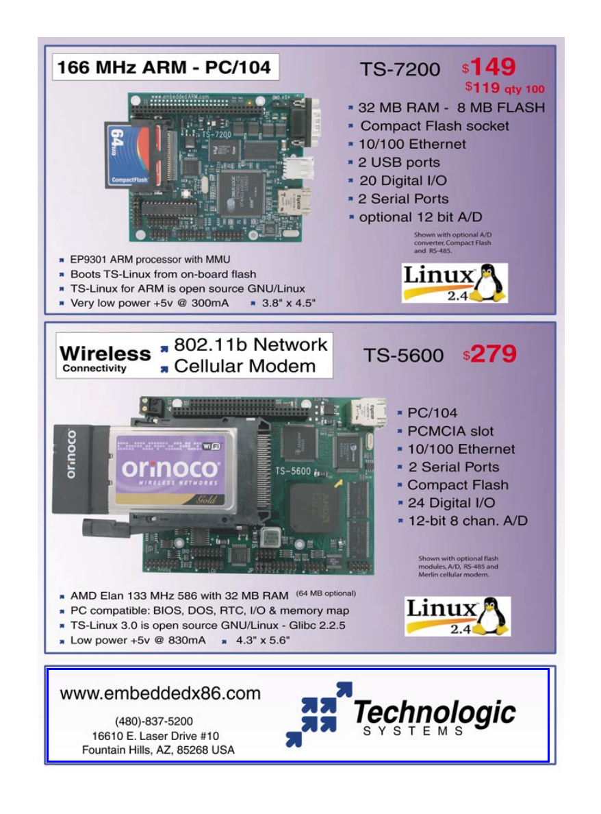
Problem 1
—
One way to measure distance is to measure
the time-of-flight of an electromagnetic signal, such as a
modulated laser beam. The time delay between the trans-
mitted signal and the received signal represents the dis-
tance traveled by the signal. What kind of time resolution is
needed to measure distances with a resolution of 1 cm?
Problem 2
—
One way to measure small time delays is to
do it in terms of the phase shift of a sine wave signal. For
example, if you modulate the beam with an 83-MHz sine
wave, which has a wavelength of approximately 3.6 m, one
degree of phase shift represents about 1 cm of distance.
Emitter
ω
1
Display
Detector

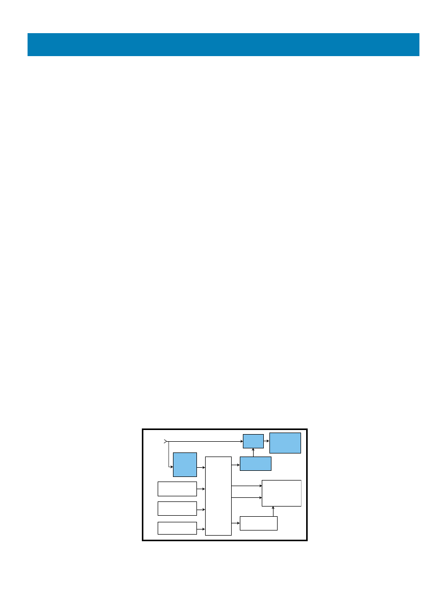
the PIC is doing, you must examine
the hardware it controls. The project
is constructed on two circuit boards
(see Figure 1). The power devices,
which are shaded in the diagram, are
mounted on the power board (see
Figure 2 and Photo 2). The logic and
LCD circuitry are included on the
logic board (see Figure 3 and Photo 3).
This design is first and foremost a
light dimmer. Phase control by way of
a triac is the simplest and least expen-
sive method available. Recall that a
triac is a bidirectional device that is
turned on (triggered) when an appropri-
ate signal is applied to its gate. It turns
off when the voltage falls to 0 V. Power
to the load is varied by turning on the
triac at the appropriate time relative to
the incoming 120-VAC power. To put it
another way, the conduction angle is
varied (see Figure 4). If the angle is set to
0°, the triac never turns on. If the angle
is set to 180°, full power is delivered to
the light bulb.
To perform the phase control
of an AC waveform, the PIC
must provide a properly timed
trigger to the triac. Consequently,
it must monitor the power line.
Specifically, it must know when
the AC waveform is at the zero
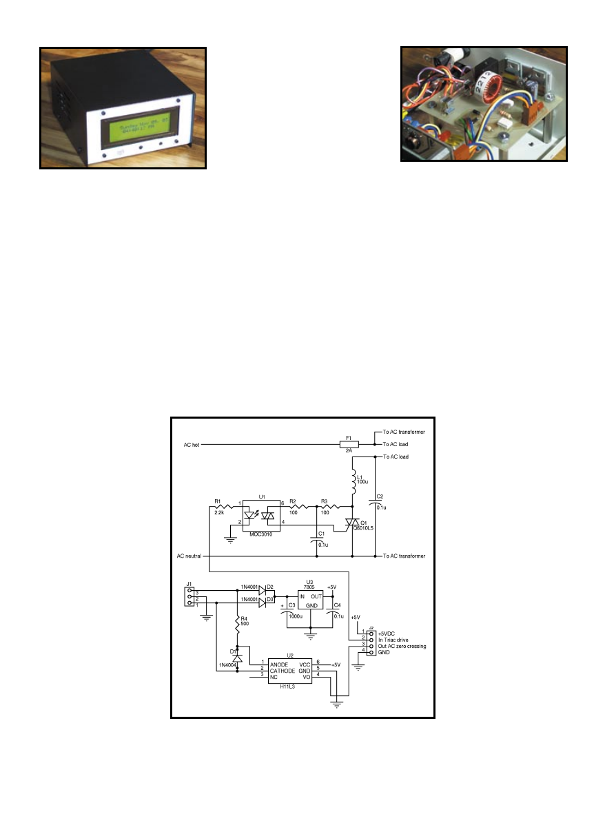
crossing. Optocoupler U2 is con-
figured as a polarity detector (see
Figure 2). It outputs a 5-VDC
logic signal if the AC waveform
is positive, and logic 0 if the sig-
nal is negative. The H11L3 pro-
vides hysteresis to prevent false
triggering. Note that the PIC is
18
Issue 170 September 2004
CIRCUIT CELLAR
®
www.circuitcellar.com
I
nspiration sometimes comes from
strange places. Consider the following,
for example: I kept goldfish when I
was a kid. My setup wasn’t elaborate.
I had three goldfish in a 20-gallon
aquarium, which had a timer-con-
trolled light bulb that would turn it
on and off at a certain time each day. I
remember thinking that it would be
better for the fish if the light gradually
turned on in the morning. After all,
the fish looked stunned (if a fish can
look stunned) when the light turned on.
Many years later, I find that I am
just like those fish. I don’t like being
stunned in the morning. It’s hard to
get up and turn on the light in the
morning, especially during the dark
Minnesota winters. So, I did some-
thing about it. I built the Sun Alarm
(see Photo 1). The small alarm con-
trols the intensity of a 120-VAC
incandescent light bulb. The light
bulb starts to turn on at a predeter-
mined time each day. The inten-
sity gradually builds to its full
level over a 30-min. period.
In addition to the automatic
sunrise feature, I included an
infrared remote control interface
for convenience. Having the
ability to turn off the lights
without getting out of bed is a
nice feature! Setting the alarm
and clock using the remote con-
trol is convenient. The IR
remote is also beneficial from a
design standpoint because it
simplifies the user interface. I
didn’t have to mount switches
The Engineer’s Alarm Clock
Aaron always wakes up to a rising sun, regardless of the weather outside. How’s that possi-
ble? He designed a PIC18F252-based alarm system that gradually brightens a 120-VAC
bulb over a half-hour period.
on the unit. This greatly simplified the
construction process and the design is
cleaner as a result. I also added an auto-
matic day/night setting for the LCD
backlight because I found the display
objectionably bright at night. Finally,
note that I included a calendar function.
In this article I’ll take you step by
step through the design process.
Together, we will explore the design
specifications, hardware implementation,
and general software functions. When
appropriate, I’ll detail the reasons why I
chose a particular design or software
approach. I’ll apply some extremely pow-
erful mathematical tools including curve
fitting, integral calculus, and Newton’s
method for calculating the roots of an
equation. With that said, let’s take a
look at the hardware inside the alarm.
HARDWARE
A PIC18F252 controls the alarm.
Before you can truly appreciate what
FEATURE ARTICLE
by Aaron Dahlen
Triac
120-VAC
Incandescent
lamp
Triac driver
MOC3010
AC Zero-
crossing
detector
H11L3
Panasonic 40-kHz
IR detector
CdS
Sensor
Real-time clock
DS1302
PIC18F252
Data
Contrast
LCD
Optrex DMC
Series
four-line
Switching power
supply
120 VAC
Backlight
intensity
Figure 1—
The Sun Alarm was constructed on two circuit boards. The
shaded items are located on the power board. The remainder of devices
are located on the logic board.
Design a PIC-Based Lamp Controller
www.circuitcellar.com
CIRCUIT CELLAR
®
Issue 170 September 2004
19
circuit serial debugger (ICD-2) and an
infrared sensor for remote control.
Our discussion of the hardware is
complete. Now let’s look at the PIC
and its interface to the hardware.
This project is an exercise in adding
functions to the PIC. To recap, the PIC
must read the real-time clock, update
the LCD, detect valid commands from
the infrared sensor, control the display
contrast, and control the intensity of
the LCD backlight. At the same time, it
must continue to monitor the 60-Hz
power line and fire the triac
at the appropriate time. This
is a big order for a micro-
processor. But it hardly
touches the capabilities of
the PIC18F252.
All of these processes
must be integrated so as to
appear simultaneous.
These timing requirements
cannot be underestimated.
I used one microcontroller,
so it was absolutely essen-
tial I understood and
accounted for the timing
issues. These software
requirements come in two
flavors: time-critical func-
tions and those that are
not. The timing for triac
control and the software
that receives the IR remote
control signal are examples
of time-critical functions,
whereas updating the dis-
play and retrieving data
from the real-time clock
are not time critical. The
PWM control of the LCD
set up to interrupt every time the out-
put of the opticoupler toggles.
The triac interface circuit is the
quintessential light dimmer circuit.
The triac drive signal is isolated from
the PIC using a MOC3010 optocoupler.
A simple EMI filter is formed by C2
and L1. Naturally, I added an internal
fuse for an additional level of safety.
Now that I’ve covered the power
interface board, let’s have a look at the
logic board. A Dallas Semiconductor
DS1302 real-time clock serves as the
timepiece (see Figure 3).
The DS1302 is a complete
real-time clock that pro-
vides the time, as well as
the day of the week, month,
and year. It has 31 bytes of
general-purpose RAM,
which is used to store the
alarm setting. Furthermore,
it communicates with the
PIC via a three-wire serial
interface.
A good clock should be
able to remember the time
when the power fails. The
DS1302 performs excep-
tionally well in this
regard. It is a low-power
device, so it doesn’t
require much of a power
source. In this design, a
1-µF capacitor serves as
the power source when
the power fails. In hind-
sight, this is overkill.
Using only the capacitor,
the DS1302 can keep time
for weeks. It’s extremely
low power indeed!
As an aside, keep in mind that the
PIC is perfectly capable of keeping
time. All you have to do is add a
32.768-kHz crystal to port C and write
some code. However, for this project,
the cost of the DS1302 was deemed
less than the time required to code
the real-time function into the PIC.
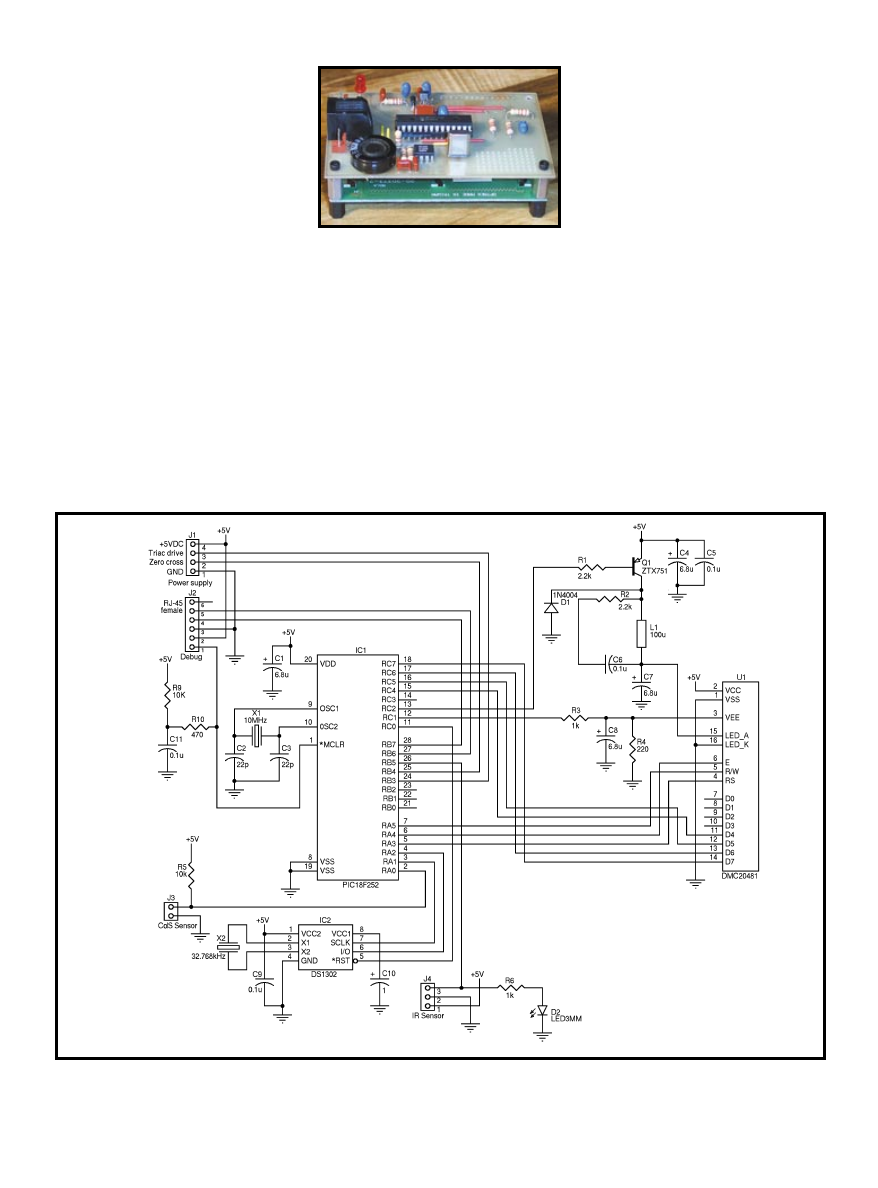
The logic board contains three cir-
cuits for operating the LCD. The first
is a nibble-wide data bus plus the
familiar E, R/W, and RS lines. The
second circuit is a contrast control for
the LCD. The PIC pulse-width modu-
lator (PWM 2 on pin RC1) is used to
control the intensity. Resistors R3,
R4, and capacitor C8 integrate the
PWM signal and step it down to a DC
voltage suitable for driving the LCD
contrast. The last circuit associated
with the LCD is a power supply for
the LCD backlight. A buck switched-
mode power supply was chosen for
this application. Transistor Q1 and
diode D1 are used as the switching
components. Inductor L1 and C7 are
the energy storage and filter elements.
The remaining circuitry consists of an
RJ-45 connector for the Microchip in-
Photo 1—
The Sun Alarm doesn’t contain any switch-
es. Control is performed with an infrared light. The IR
sensor is centered below the LCD. A CdS light sensor
is positioned to the left of the IR detector. The lens for
the CdS sensor was taken from a nightlight.
Figure 2—
The power board contains the quintessential optoisolated triac circuit. In
hindsight, it would have been better to place the triac on the hot side of the AC line.
This provides an additional margin of safety (i.e., when the triac is off, no AC voltage is
applied to the load terminal).
Photo 2—
The power board consists of the 5-VDC reg-
ulator, triac, and supporting circuitry. Optoisolators are
used to isolate the logic board from the AC line volt-
ages. The enclosure is used as a heatsink. A large
toroidal power transformer is mounted under the left
front corner of the board.
circuits is not time critical because
the PWM functions are handled by the
PIC’s hardware PWM.
The PIC18F252 presents an elegant
solution to these timing issues. You
can use interrupts! Recall that when a
CPU is interrupted, it stops executing
the main program and jumps to the
interrupt service routine (ISR). When
the ISR is complete, the CPU returns
to the original task. The time-critical
tasks in this project are handled by the
ISR, and the tasks that aren’t time-
critical are performed in the mainline
code. This is ideal because the ISR has
priority over the mainline code.
As an example, assume the PIC is
performing a non-time-critical task
such as updating the LCD. Also, assume
that a timer has been set up to interrupt
the CPU when it is time to fire the
triac. When the timer has timed out, it
interrupts the CPU, which responds by
20
Issue 170 September 2004
CIRCUIT CELLAR
®
www.circuitcellar.com
vectoring to the ISR. The ISR starts
the triac pulse. When the ISR is done,
the PIC18F252 returns to where it left
off with the LCD update routine.
The PIC18F252 has many built-in
features associated with the inter-
rupts. It may be interrupted by an
external stimulus or one of its own
internal peripherals. Both types of inter-
rupts are used in this project. External
interrupts are used to interrupt the PIC
when an IR signal is received and to
synchronize it to the 60-Hz line fre-
quency. Internal interrupts from the
PIC timers are used to set up the timing
delays for triac firing. The PIC also
automatically saves special registers.
(Note that only Microchip’s high-level
interrupts are used in the project.) Now
let’s look at two time-critical func-
tions that are performed by the ISR.
I follow a simple philosophy when
using the ISR: make it fast! The short-
er the better. Don’t wait around for
something to happen. You will never
find software delays in my ISRs. Any
delays in the ISR could cause delays in
the mainline code; or, worse yet, they
could prevent some other function of
Figure 3—
The logic board contains a real-time clock (IC2) complete with a 1-µF capacitor backup. A 4-bit data bus is used to interface with the LCD. A buck power supply
provides variable intensity to the LCD backlight. Transistor Q1 is controller by the PIC18F252 PWM. The contrast of the LCD is also controlled by the PIC18F252’s PWM (LCD
V
EE
line). Finally, connections are provided to interface with the power board and the ICD 2.
Photo 3—
The logic board is piggybacked on the LCD.
The real-time clock and the 1-µF backup storage capaci-
tor are seen the in the foreground. The 32.768-kHz
oscillator crystal is surface-mounted beneath the logic
board. The PIC18F252 and the ICD 2 connector (RJ-
45) are in the middle of the board. The inductor for the
LCD backlight buck power supply is also surface-
mounted to the board.
www.circuitcellar.com
CIRCUIT CELLAR
®
Issue 170 September 2004
21
the ISR from occurring. For example,
as you work on the Sun Alarm project,
you can’t wait around for the infrared
detector to do something because the
PIC must be ready to fire the triac. Keep
this in mind as you review the source
code posted on the Circuit Cellar ftp
site. Because of the time requirements,
the ISR tends to be a bit complex.
Global variables complicate the process,
but they are necessary to hold interme-
diate values. Also, if the ISR requires a
delay, the timers will handle it.
PHASE CONTROL
Two general functions are necessary
to implement the phase control of an
AC load using a microprocessor. First,
the microprocessor must synchronize
itself with the 60-Hz power line.
Secondly, the microprocessor must
determine the power to be delivered to
the load. The brawn of controlling the
triac is implemented a in the ISR. This
implementation is based entirely on
time. The timing of the triac fire pulses
must coincide with the 120-VAC
power line. Any timing deviations will
be detected as the flickering of the light
bulb. The decision-making process that
determines intensity is located in the
mainline code because it is not a time-
critical function.
The power delivered to the load
(light bulb) is controlled by varying
the conduction angle of the applied
AC signal (see Figure 4). Note that if
the conduction angle is small, a small
portion of the AC signal is sent to the
load. If the conduction angle is large,
the majority of the incoming signal is
sent to the load. If you assume a 60-Hz
signal, the conduction angle will vary
from 0 to 8.33 µs. Refer to the
“Calculating Phase Angles” sidebar
for more information about calculat-
ing the conduction angles.
The incoming AC waveform is
monitored using an opticoupler (see
Figure 2). The monitored voltage is
taken off the step-down transformer.
The opticoupler signal is sent to port B
on the PIC18F252, which is programmed
to vector to an ISR when the pin changes
value. When a zero crossing is detect-
ed, the PIC18F252 starts a countdown
via Timer3. The value loaded into the
timer is determined by the mainline
code; actually, the main code passes
an index pointer to the ISR. When the
Timer3 countdown is complete, the
triac is fired with a 1.5-µs pulse. The
process involves four phases: wait for
an AC signal zero crossing; load the
timer with a delay equal to the desired
conduction angle; fire the triac when
the timer delay is complete; and
repeat these steps indefinitely.
INFRARED CONTROL
This project uses a Sony protocol.
Specifically, it mimics a Sony DVD
player. The reason for selecting the
Sony protocol was totally arbitrary; it
was the remote control I had at home.
The remote’s arrow buttons (menu
buttons) command the project. The up
and down arrows control the light
bulb intensity. These arrows, along
with the left arrow, are used to set the
clock and alarm times. Finally, the
DVD Menu Select button is used to
select the set time and alarm menus.
The infrared remote control detector
is the second time-critical function
performed as the ISR. I use the word
“critical” loosely because the Sony IR
data is sent using a 550-µs timebase,
which is an eternity for the PIC18F252.
Figure 5 shows the protocol used by
the Sony IR remote control. It’s a seri-
θ
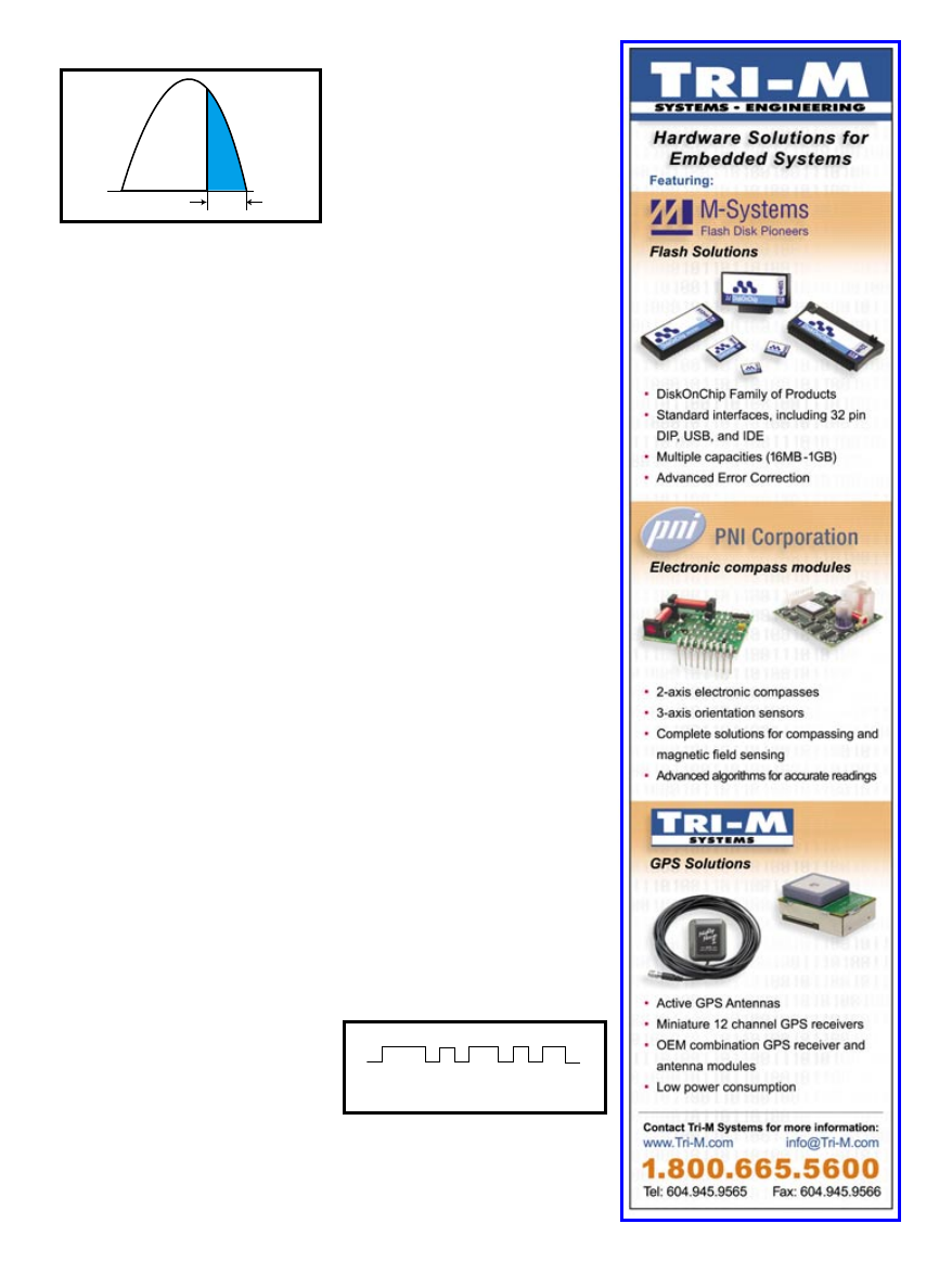
Figure 4—
Phase control is achieved by firing (turning
on) the triac at the appropriate time relative to the
incoming AC voltage. After the triac is fired, it remains
on (conducting) until the AC line voltage returns to
zero. Consequently, the right side of angle
θ
is fixed.
Only the left side is free to move.
Header
4T
0
T
1
2T
0
T
1
2T
Figure 5—
The Sony infrared remote control uses a vari-
able
pulse-width code. The width is based on time (T),
which is 550 µs. Each command begins with a header
(4T = 2,200 µs). A logic 0 has a pulse width of T =
550 µs. A logic 1 has a pulse width of 2T = 1,100 µs.
22
Issue 170 September 2004
CIRCUIT CELLAR
®
www.circuitcellar.com
is used to differentiate the various
logic levels. Logic 0s are length T.
Logic 1s are length 2T. I found it inter-
al protocol sent LSB first. Every serial
string starts with a header of length
4T (i.e., 2,200 µs). Variable pulse width
esting that Sony uses a different num-
ber of bits depending on the type of
device. The protocol for a TV contains
Calculating Phase Angles
The phase control of a triac is conceptually simple. All
you have to do is wait for the zero crossing of an AC
waveform, wait an appropriate amount of time, and
then trigger the triac. The hard part is determining how
long to wait! Let’s explore the steps required to calculate
the time delays (a.k.a. conduction angles). My final solu-
tion was to write a computer program (Python) that per-
forms the calculation. You may download the program
from the Circuit Cellar ftp site. To understand how this
script works, you must first understand the math.
The first step is to make an assumption. I speculated
that intensity of a light bulb is approximately proportion-
al to the power it consumes. Double the power and the
lamp should be twice as bright. Brightness is a subjective
term because none of us have calibrated eyeballs.
However, a simple solar cell may be used to measure
luminosity. With this setup, I determined that my initial
approximation is mostly true: intensity is proportional to
power. A supporting graph is shown as Figure 1.
I know what you are saying: it isn’t linear for low drive
levels. That’s because the light bulb changes color. At low
drive levels, the lamp is a dull red color. The solar cell
is not sensitive to this color; therefore, the graph is
nonlinear at low levels. Also, the lamp requires a finite
amount of power before it will emit light. An observation
with my noncalibrated eyeballs suggests that the linear-
ity is preserved in this low range.
You can calculate the power with Equation 1:
[1]
where R is the resistive load. But things get complex
because the light bulb has a nonlinear resistance (see
Figure 2). This is great if you are building a Wien-bridge
oscillator, but it isn’t so good if you want a linear lumi-
nosity response from the light bulb. Not to fear, the resist-
ance may be approximated by a second-order equation
with resistance defined in terms of voltage. Many pro-
grams are available on the ’Net to perform this operation.
Equation 2 is for a 240-W light bulb:
[2]
The line representing this equation is shown superim-
posed on the measured resistance in Figure 2. Higher-
order equations can be a better fit, but the added com-
plexity isn’t warranted. Equation 2 is substituted into
Equation 1 to yield Equation 3:
[3]
If P = 100 W,
then 1.21e + 64.23e + 1,565.13 = 0
2
−
R = 0.0021e + 0.6423e + 15.6513
2
−
P
e
R
=
2
Please note that you are solving for 100 W. Also, all
measurements and calculations are expressed as RMS
values. The quadratic equation is used to provide a solu-
tion:
[4]
The negative result is discarded. Using this method, you have
a solution for the required voltage at any given power.
The next step is to determine the phase angle for a given
voltage. You need to go back to the basic equations. Recall
that the AC sine wave is defined as Equation 5, and
Equation 6 defines the RMS voltage:
[5]
v t
t
( )
= V
MAX
sin
ω
V
RMS
=
V
= 71.2
RMS
−
±
− −
(
)(
)
−
(
)
64 23
64 23
4
1 21 1 565 13
2
1 21
2
.
.
.
,
.
.
and
−
18 2
.
1.200
1.000
0.800
0.600
0.400
0.200
0.000
0
10
20
30
40
50
60
70
80
90
100
Percent drive
Cell output v
oltage
240 W
60 W
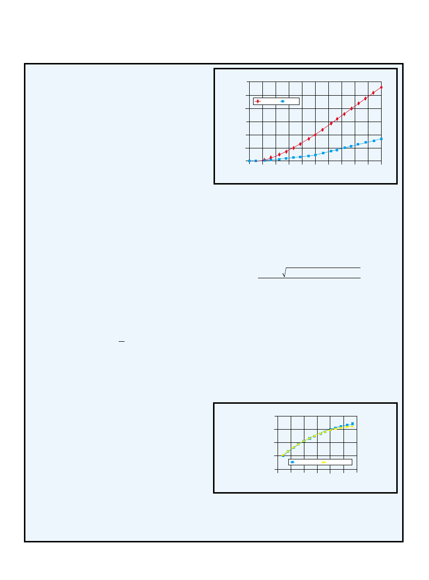
Figure 1—
The ability of the Sun Alarm to linearly control the brightness of a light bulb is
demonstrated in this graph. The intensity of the light bulb is determined by measuring the
output voltage of a solar cell. The nonlinearity at low drive levels is the result of the color
change of the light bulb. The solar cell is not sensitive to the reddish color of a dim light bulb.
80
60
40
20
0
0
25
50
75
100
Resistance
(Ohms)
AC RMS voltage
125
150
Measured
Calculated
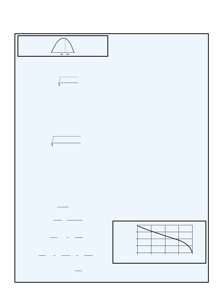
Figure 2—
The resistance of a light bulb is not constant! Resistance is a nonlinear
function of the applied voltage. Measuring the voltage across and the current through
a light bulb derived the data. A variac was used to change the applied voltage. The
calculated data is derived from a second-order equation. A curve-fitting program
computed the coefficients based on the measured data.
www.circuitcellar.com
CIRCUIT CELLAR
®
Issue 170 September 2004
23
12 bits, while the DVD protocol con-
tains 20 bits.
The PIC is set up to interrupt on
then returns to the mainline code.
When the IR signal is no longer pres-
ent, the PIC is interrupted again.
every changing edge of the IR sensor.
If the IR is active (IR signal present),
the PIC clears and starts Timer1. It
[6]
This is going to get complicated, so do yourself a favor and
simplify the math. First, do all the calculation is radians.
Secondly, normalize the equations by letting
ω
= 1.
When you do this, f = 1/2
π
and the period becomes 2
π
. A
half cycle of the AC signal is shown in Figure 3. The sig-
nal starts at zero and continues to pi radians.
Here’s where the fun begins. You need to calculate
θ
for a given RMS voltage. The relationship is shown in
Equation 7.
[7]
Recall that the triac turns on when triggered and turns off
when the waveform falls to zero. Here I will refer to the trig-
ger point as
θ
radians. When
θ
equals zero, full power is
applied to the load. Likewise, as
θ
approaches pi, no power is
delivered to the load. This may appear backwards at first
glance. But remember, the part I’m interested in what occurs
after the triac is triggered. Therefore, integrate from
θ
to pi.
The derivation of Equation 7 is shown in Equations 8
through 12. I used a trigonometric substitution in
Equation 9. Equation 10 shows the integration. The
Fundamental Theorem of Calculus is used in Equation 11.
[8]
[9]
[10]
[11]
[12]
2
2
2
θ
θ
π
π
= 2 4
−
−
sin
V
V
RMS
MAX
π
π
π
θ
θ
V
V
RMS
MAX
−
−
−
2
2
2
4
2
2
4
=
sin
sin
π
θ
π
V
V
t
t
RMS
MAX
−
2
2
2
4
=
sin
V
V
t
dt
RMS
MAX
2
2
1
2
2
=
π
θ
π
−
∫
cos
V
V
tdt
RMS
MAX
2
2
2
=
(
)
∫
π
θ
π
sin
V
V
tdt
T
RMS
MAX
=
(
)
∫
2
2
sin
ω
θ
π
V
Area v t
T
RMS
=
2
( )
Equation 12 is an interesting animal. After close examina-
tion, it’s clear that the values on the right-hand side of the
equation are between zero and 2
π
. Recall than that V
RMS
may be no more than 0.707 of V
MAX
. If you allow the right-
hand side of the equation to equal N, then 2
θ
– sin2
θ
= N,
where 0 < N < 2
π
. At first glance, this looks like a simple
equation, but it’s actually a monster. There is no good
way to get
θ
out in the open. You must use a numerical
method. Two algorithms come to mind, the brute-force
successive approximation and Newton’s method. Of the
two, the latter is preferred. It is an elegant solution that
quickly returns a result.
Newton’s method was implemented as a recursive algo-
rithm. This is a most impressive solution and a testament
to Newton’s genius. It’s one of those algorithms you must
see to believe. In my implementation,
θ
is solved to 10
decimal places in less than eight recursions!
The final results of this method are shown in Figure 4.
The phase angle is seen to change little for angles close to
pi. In fact, when the phase angle is
π
/2, the output voltage is
approximately 80 V. From this point, the conduction angle
rapidly converges to its maximum value of zero.
All of the phase angle calculations were performed with a
Python program. If you haven’t used it, note that Python is a
wonderful introductory programming language. Best of all
it’s free! You can download a copy at www.python.org.
Keep in mind that my Python script must run from the
GUI interface. I didn’t bother saving the data to a file
because the data is cut and pasted to MPLAB.
Recap
Wasn’t that fun? Let’s review the steps. First, calculate
an equation that describes the nonlinear resistance of the
light bulb using empirical data and a curve-fitting pro-
gram. Then, determine the RMS voltage for a given power
using the quadratic equation. Finally, calculate the phase
angle using integral calculus and Newton’s method. That’s
all there is to it! I must confess this approach took a great
deal of time and effort—more than I care to remember.
0
θ
π
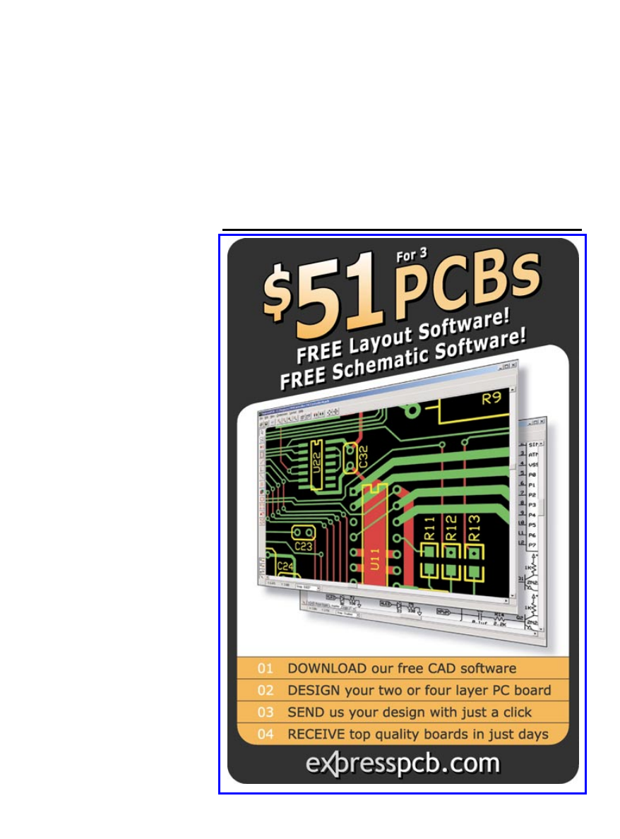
Figure 3—
Changing the conduction angle
θ
controls the power delivered to the
load. The math is simplified by using radians. That’s why you see the angle
θ
expressed as a number between zero and
Π
.
3.20
2.40
1.60
0.80
0.00
0
30
60
90
120
Phase angle (r
adians)
RMS voltage
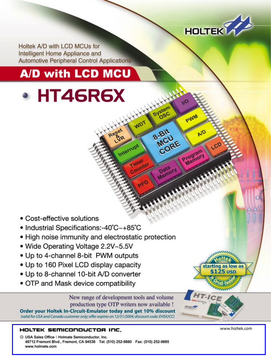
Figure 4—
By solving Equation 12 for all angles between zero and
Π
, you arrive at
the nonlinear solution presented here. Recall that the angle
θ
is a starting point.
The triac turns on at
θ
and off at
Π
.

www.circuitcellar.com
CIRCUIT CELLAR
®
Issue 170 September 2004
25
Timer1 is read, and a decision is
made based on the value accumulated
in Timer1. If the time is less than
350 µs, the received pulse is not valid.
If 350 < T < 880 µs, the pulse is a logic 0.
For 800 < T < 1,100 µs, the pulse is a
logic 1. And, finally, if the time is
greater than 1,600 µs, the pulse is
assumed to be a header.
Recall that one of the objectives for
the efficient use of the ISRs is to spend
as little time in them as possible. This
makes the IR routine a bit problematic.
The received serial word must be built
over several iterations of the IR rou-
tine. Each pulse in Figure 4 interrupts
the PIC two times: once when it’s
asserted and once when it’s released.
Several global variables are used to
build a new command. A global vari-
able called
command holds the incom-
ing serial bit stream. The MSB of
com-
mand is set to the value of the
received byte each time a new bit is
received.
command is shifted to the
right after the receipt of every bit. A
global variable called
IR_bit_cnt is
used to keep track of the number valid
bits received. If errors occur in the
reception of an IR word, the
IR_bit_cnt is cleared. It will be
cleared when a runt pulse occurs and
when a header is detected.
The ISR and the mainline code must
be coordinated. A new_command flag is
used to signal to the mainline code that
a new IR sequence has been received.
This flag is set after the ISR has received
15 valid bits. After the ISR sets the flag, it
effectively disables itself. It won’t receive
any additional IR commands until the
mainline code acknowledges the new
command by clearing the new_com-
mand flag. Because this type of sema-
phore is used, the global variable com-
mand may be used to pass the received
IR command to the mainline code. A
debounce function is also performed by
the ISR. After a valid command is
received, the ISR will not receive any
new command for a period of 0.2 s.
This concludes my description of
the ISR routine. Now let’s examine
the mainline code.
LINEAR POWER
Now that you know how the PIC
controls the triac, let’s look at how
the microcontroller determines the
intensity. As previously stated, the
power delivered to the load is adjusted
by varying the conduction angle (tim-
ing) of the AC sine wave. It is tempt-
ing to simply slice the wave into equal
blocks of time. However, this
approach is undesirable. The power
delivered to load is not linear. There
are two reasons for this nonlinearity.
First, the RMS power is not a linear
function of the phase angle. Secondly,
the resistance of the light bulb varies
with the applied voltage. Refer to the
sidebar for more information.
Now that you have an understand-
ing of the mathematics of calculating
the conduction angle, let’s look at how
to apply it to the microcontroller. A
base requirement for this project was
to ramp the intensity of a light bulb
over a 30-min. period. Because a con-
venient 1-pps clock was available, I
chose to have 1,800 individual power
levels (30 min. × 60 s). There are two
methods to achieve this objective.

26
Issue 170 September 2004
CIRCUIT CELLAR
®
www.circuitcellar.com
triac fired. The PIC18F252’s Timer3
maintains the delay. To simplify the code,
all the hard work was done in Python.
Each data point is formatted to load
directly into the Timer3. The only func-
tion remaining for the PIC is to select and
maintain an index pointer to the desired
conduction angle stored in the data table.
TIME DISPLAY
The real-time clock functions
account for the majority of the code
associated with this project. There are
three main tasks that must be performed
with respect to the real-time clock: read
and send data to the LCD, update the
time clock, and update the alarm.
The code to interface with the real-
time clock was built from the bottom
up. Recall that the DS1302 real-time
clock is a three-wire synchronous seri-
al device. The base functions transmit
and receive byte width data. More
complex functions such as updating
the months register are built on top of
these functions. The use of aliases
greatly simplifies the code. For exam-
ple, the months register is referred to
as MONTH instead of 10001000.
The LCD software routine is loosely
adapted from the Microchip C18
library. I added additional functions
on top of the basic functions to make
programming faster and easier. A
prime example is the following line:
Put_ROM_LCD (“Hello World”,
line_2, 5);
The PIC18F252 will take the text
“Hello World” from ROM and send it to
the LCD. The text will appear on the
second line and will be offset five spaces
to the right. True, it isn’t the most time-
and space-efficient method, but neither
is a requirement in this application.
Figuring out how and when to
update the display is an interesting
challenge. The display looks some-
thing like this in Normal mode:
Saturday Nov 12, 03
11:10:23 PM
Obviously, the display doesn’t need to
be updated more than once per second.
A function was designed to monitor the
seconds register of the real-time clock.
The main line code essentially spins in
a loop until the seconds register of the
real-time clock changes. When it final-
ly does, the LCD is updated.
The method used to update the dis-
play is crude but effective. The first
step is to retrieve a register from the
real-time clock (e.g., the month regis-
ter). This date is in a BCD format so
it’s sent to a function that converts it
to a decimal number. The resulting
number is used as the index for a
switch statement. Each case contains
First, the data could be coded into a
look-up table. Secondly, an equation
could be implemented. Because of the
complexity of the equation, I decided to
go with a look-up table. The table con-
tains 1,800 16-bit words. The entire
program, including data table, con-
sumes only 25% of the PIC18F252’s
ROM. Obviously, the Python script
mentioned in the sidebar is a necessity.
Recall that the purpose of this data
table is to provide a delay between the
time a zero crossing is detected and the
www.circuitcellar.com
CIRCUIT CELLAR
®
Issue 170 September 2004
29
a
Put_ROM_LCD statement similar to
the one I described earlier.
Updating the real-time clock registers
is more complex. The basic procedure
is performed as a read/modify/write
operation: a register is read from the
real-time clock, modified (incremented
or decremented), and then written back
to the real-time clock. This is where
the real-time clock gets interesting. It
doesn’t check the validity of the data.
For example, if you tell it that it is the
thirty-fifth of March, it just keeps on
going. Consequently, the PIC18F252
must check the validity of each num-
ber you enter.
The adjustments to the clock and
alarm are made as simple up/down
changes to each register. For example,
if you want to adjust the hours regis-
ter, a blinking cursor will appear
under the hours display:
Set Clock
Saturday Nov 12, 03
11:10:23 PM
You will then use the up or down arrows
to increment or decrement the hours. A
right arrow will move the cursor to the
next category (minutes in this example).
It is vital that the PIC18F252 vali-
date each number before it is stored
back in the real-time clock. Each cate-
gory must be checked against a mini-
mum and a maximum. The months
register, for example, always must be
between one and 12. Remember that
the DS1302 stores everything in BCD
format. If the register is at 12 and you
push the increment button, the value
of one will be stored in the real-time
clock. If it’s less than 12, the number is
incriminated. A similar function is pro-
vided for decrementing the numbers.
Updating the real-time clock and
alarm is done using a state function.
When you push the DVD Menu but-
ton on the remote control, the pro-
gram vectors to the update_clock
function. This function then calls
individual functions to update the
various real-time clock registers. Note
that the ISR continues to function in
the background. The light (triac phase
angle) remains at its present setting;
however, you will no longer be able to
manually adjust the intensity.
Each sub-function updates the dis-
play as necessary, responds to user
increment/decrement commands, and
finally moves to the next category if
you press the right arrow button. Each
sub-function contains the appropriate
minimum and maximum for the cate-
gory and conversion to and from BCD
and binary. I found it easier to convert
everything to binary, increment/decre-
ment as necessary, and then convert
back to BCD. Again, by no means is
this the most efficient method.
However, it’s simple and there is no
performance penalty in this application.
BACKLIGHT SETTINGS
The contrast and backlight intensi-
ty are under the direct control of the
PIC18F252. Both are connected to the
PIC18F252 PWM outputs. For this
project, the PWM that controls the
contrast is set once and never adjust-
ed. I had originally thought it would
be useful to have the ability to adjust
it using the remote control. However,

30
Issue 170 September 2004
CIRCUIT CELLAR
®
www.circuitcellar.com
I found no need to adjust the contrast.
The intensity of the LCD backlight is
set using the first PWM. A buck-type
switcher converts the PWM to DC level
suitable to drive the LCD backlight.
The backlight has a day and night set-
ting. A cadmium sulfide sensor (CdS) is
used to detect the ambient light levels.
The PIC18F252 reads the sensor using
the first channel of the A/D converter.
An if-else statement is used to set the
PWM that drives the LCD backlight. If
the A/D conversion is above the
threshold, the display is bright (day);
otherwise, it is set to dim (night).
EVERY SEASON
The PIC18F252 has the memory,
speed, and built-in peripherals to easi-
ly perform all of the functions
required for this design. Microchip
has powerful debugging tools. The in-
circuit debugger (ICD 2) greatly sim-
plified the code debugging. With the
ICD 2, you can see what the code is
doing. You can set breakpoints, view
the contents of registers, and step
through the code line by line. Also,
simply having the ability to program
the device in-circuit saves time.
I wrote the code with Microchip’s
C18 compiler. This is hands down the
best way to program the PIC18F252.
In the past, all of my programs were
written in assembly language with
MPLAB. They worked, but it was
extremely time-consuming to code
even simplest functions. That all
changed with the C compiler. The
code’s layout is simpler. There are
fewer lines of code, and it’s extremely
easy to reuse functions. If you’re still
coding in assembly language, do your-
self a favor and spend the time and
money to purchase the C compiler.
It’s definitely worth the expense.
There you have it—the Sun Alarm!
I have been using this device for sev-
eral months now and it works won-
derfully. The best compliment I
received came from my wife. She said
she didn’t even know it was there. We
have a bedroom that faces east. In the
summertime, the sun wakes us up
every morning. In the winter, my artifi-
cial sunlight announces the new day.
I
PROJECT FILES
To download the code, go to ftp.circuit
cellar.com/pub/Circuit_Cellar/2004/170.
SOURCES
DS1302 Real-time clock
Maxim Integrated Products
(800) 998-9872
www.maxim-ic.com
PIC18F252 Microcontroller
Microchip Technology, Inc.
(480) 792-7200
www.microchip.com
DMC20481 LCD
Optrex America, Inc.
(734) 416-8500
www.optrex.com
Aaron Dahlen is a recent E.E.T. grad-
uate from Minnesota State University,
Mankato. He is currently serving his
country in the United States military.
In his spare time, Aaron builds proj-
ects with microcontrollers and vacu-
um tubes. You may reach him at
apdahlen@hotmail.com.


quency (if available) would drive the
motor speed to the desired torque and
angular speed specifications, preserv-
ing the linear relation between fre-
quency and fundamental line-to-line
RMS voltage. For instance, if the line-
to-line RMS voltage is 220 at 60 Hz,
the line-to-line RMS voltage would be
109.99 at 30 Hz. At 10 Hz, the line-to-
line RMS voltage would be 36.666,
and so on. But in industry, variable
sinusoidal signals aren’t cost-effective.
(They represent a complicated AC
source.) Varying the width of pulses and
frequencies achieves similar results.
There are various PWM techniques,
including variations of the same
SPWM.
[2]
What changes in the differ-
ent SPWM cases is the reference or
control signal. In one case, the modu-
lation makes use of a sinusoidal modi-
fied with injected harmonics. In
another, the reference is a trapezoidal
signal. But despite these differences,
every modulation technique uses a tri-
angular signal as a carrier signal.
Common SPWM modulation is
done in amplitude. Although the use
of a triangular signal as carrier is
inherited from the analog
world, this is a predominantly
digital world. So, we thought
about ways to get the most
out of new microcontrollers
and DSPs.
We didn’t want to use a
triangular signal as carrier just
to generate the SPWM signal
with the microcontroller’s
resources (in a pure algorith-
32
Issue 170 September 2004
CIRCUIT CELLAR
®
www.circuitcellar.com
S
ometimes well-known, established
concepts may provide elements to
develop new algorithms. In some
cases, the new algorithm might sur-
prise you for its relative ease of imple-
mentation and good performance.
We have been working for some time
to develop a variable frequency drive
(VFD) as a controller for three-phase
AC motors. During this process, we’ve
been working on a micro-programmed
approach to unipolar sine wave pulse-
width modulation (SPWM). This
approach, which we programmed and
simulated in MATLAB/Simulink (R13),
has produced good results. We chris-
tened the modulation technique as
quadrature SPWM (QUSPWM) because
of the basic nature of its generation.
The switched integration technique is
a basic equalization of areas for PWM
and the sine reference signals.
VFDs are effective AC motor con-
trollers that deliver substantial energy
savings. Because of its solid-state design,
a VFD is highly reliable and affordable.
[1]
There are several methods for con-
trolling the speed in an AC induction
motor. One technique is the frequency
control method (see Figure
1). The drive voltage is calcu-
lated from the frequency
using the volts-per-hertz
ratio, which is a linear rela-
tionship between the frequen-
cy and line-to-line RMS volt-
age applied to the AC motor.
If a change in frequency
occurs, a change in voltage
should also occur in order to
An SPWM Calculator
sustain the torque capability. The fre-
quency and voltage parameters in the
proper ratio are fed the modulator that
delivers the PWM signals to drive the
motor to a desired speed. Note that
this is an extremely basic open-loop
control scheme. But we’re not inter-
ested in the control algorithm or con-
trol scheme. We’re focusing instead on
the modulation technique.
Figure 2 shows the linear relation
between voltage and frequency.
Sinusoidal voltage amplitude depends
on either the frequency or motor speed.
Two cases are presented for 230- and
460-V
RMS
motors. Remember this rela-
tion because it will be useful to explain
and justify the QUSPWM algorithm.
QUADRATURE SPWM BASICS
The switched integration technique,
or quadrature SPWM, is simple. It
consists of the integral of the ideal
sinusoidal signal (control or modulat-
ing signal) with a pulse train whose
amplitude is given by a DC fixed
source (rectified from phase voltage).
Ideally, the variable sinusoidal signals
(three phases) in amplitude and fre-
FEATURE ARTICLE
by Armando Rosas Morato & Sergio Elizarraras Rodriguez
Sine pulse-width modulation (SPWM) is a technique frequently used in variable frequency
drives for speed control in AC motors. Armando and Sergio present the QUSPWM algorithm
as a simpler variation of SPWM based on a switched integration operation.
Frequency
reference
V/F
Ratio
QUSPWM
Modulator
AC Motor
Frequency control
V
F
Figure 1—
The frequency control AC motor has an open-loop regulation scheme in
which the motor receives a pulse train that resembles the ideal sinusoidal sourc-
ing. The angular speed of the motor must follow a linear relation with the ideal
sinusoidal amplitude, the volts-per-hertz ratio. Hence, the PWM signal should com-
ply with the aforementioned ratio.
Using the Switched Integration Technique
achieved (see Figure 3). Integration is a
linear operation (the volts-per-hertz
ratio is a linear relation too), so the
value of the original sine integral is
the same for each different frequency
case. As the integral is preserved
(amplitude and shape), the fundamental
value is preserved, attenuating harmon-
ics because the sine reference amplitude
is closer to the fixed DC pulse ampli-
tude. Clearly, this isn’t the case for low
frequencies (i.e., below 10 Hz), which is
when harmonics increases because inte-
gral equalization is hard to reach with
accuracy. Despite this poor performance
at low frequencies (increasing pulsat-
ing torque), speed control might be
achieved with good results.
Knowing that integral operation
could be the answer to regulate the
width of pulses, our first idea was to
generate the approximation during a
www.circuitcellar.com
CIRCUIT CELLAR
®
Issue 170 September 2004
33
complete semicycle. Because the total
area of a pulse is bigger than the area
of a sine semicycle, we choose to
make the pulse train generation by
doing a comparison between the inte-
grated sine and the integrated pulse
train. During the modulation, if the inte-
gral of the sine is greater than or equal to
the integral of the pulse train, the pulse
will continue on high. But, if the integral
of the sine is less than the integral of the
pulse train, the pulse will go to low and
wait until the proportion is reversed.
From this you get the designation of
“switched integration,” or quadrature.
INITIAL ATTEMPTS
With a foundation in place, imple-
mentation became the real issue (at
least in a computational way for simu-
lation purposes). Programming in MAT-
LAB, we tried the first version running
the numerical integration (trapezoidal
rule) along the first sine semicycle. It
was disappointing. Despite using small
sampling periods, we didn’t achieve
symmetry. Small errors during numeri-
cal integration induced the lack of
symmetry in the pulse train. Refer to
the “MATLAB/Simulink Platform”
sidebar for more information.
Our second attempt involved just
the first quarter cycle of the entire
sine during numerical integration. But
we were still having problems with
symmetry toward the end of the
numerical integration of the quarter
cycle. To avoid more problems, we
mic way). We thought the algorithm
should be efficient and reliable for per-
forming speed control in the widest range
of specified frequencies. Getting
through the process was the next step.
An SPWM signal must be similar to
the ideal sinusoidal reference. That’s
the main objective. We put this to
Fourier analysis in a trigonometric
Fourier expansion series. This means
that a signal with pure sinusoidal har-
monics (no DC and cosinusoidal com-
ponents)—with the fundamental value
as equal as possible to the original sinu-
soidal fundamental value and attenuat-
ed harmonics—could fit the answer.
The expansion of the trigonometric
Fourier series for the pulses doesn’t
have cosinusoidal terms (see Figure 3).
Obviously, there isn’t a DC compo-
nent. This can be achieved because of
the symmetry properties (half and
quarter of cycle). You know that the
pulses should have an odd and even
symmetry around the half and quarter
of cycles respectively. What you need
to know is how to control the width
to reflect the original fundamental
value (attenuating harmonics).
Probing with different operators to
accomplish the task, the integration
gives the best possible answer.
If the integral of the pulse train
reflects in an accurate way the inte-
gral of the sine (at the specified fre-
quency), then the fundamental value
of the original sine reference is pre-
served and speed control may be
460-V
RMS
motor
230-V
RMS
motor
0
10
20
30
40
50
60
0
100
200
300
400
500
Frequency
V
o
ltage
Figure 2—
The angular speed and sustainable torque
in the AC motor depend on a linear voltage-per-fre-
quency ratio. The ideal sinusoidal amplitude diminishes
as frequency does.
Maximum
shift
D2
D1
T/4
3T/4
T/2
T
t
QU
S
P
W
M
Amplitude
DFT(QUSPMW)
H(F)
f1
f3
f5
f7
f9
f11 f13 f15 f17
f[Hz]
……
=
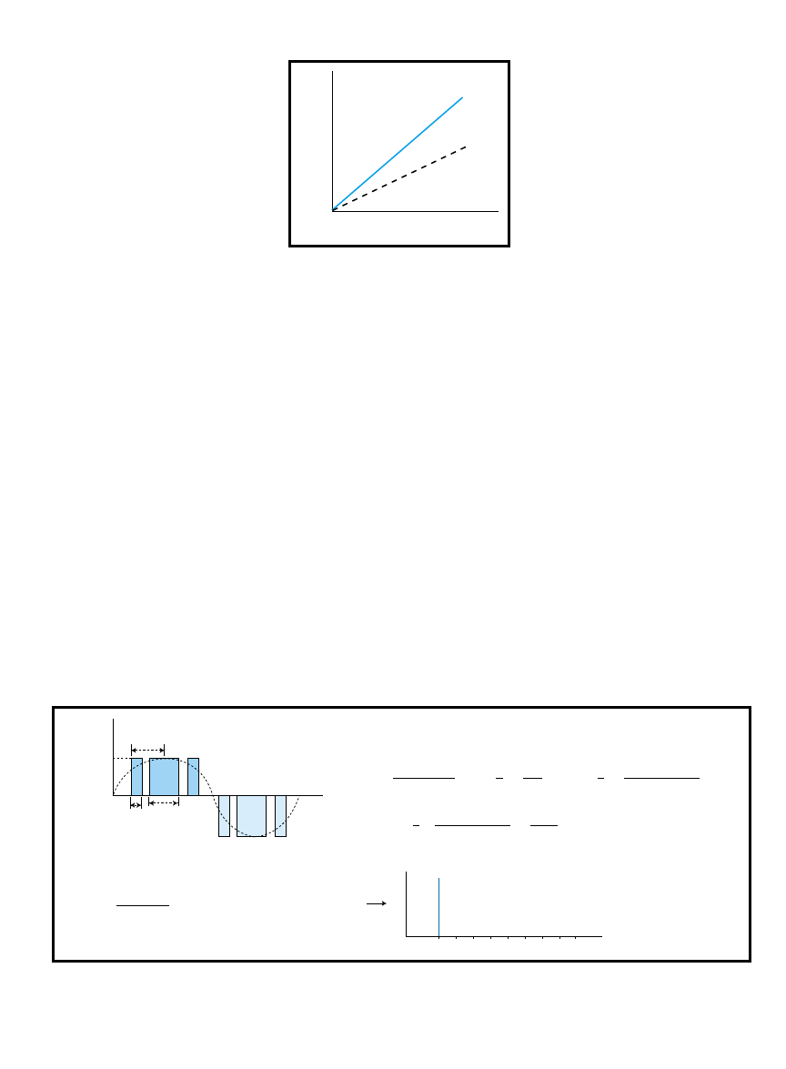
Figure 3—
Odd symmetry around the half cycle and even symmetry at the quarter of the cycle mean the QUSPWM-equivalent Fourier trigonometric series doesn’t have sinu-
soidal (even) and cosinusoidal (even and odd) harmonics. And with the switched integration as the pulse-width activation mechanism, the fundamental value of the sine wave
reference is brought on by the QUSPWM, yielding a fine approximation to the original sine reference.
4
2
1
2
2
1
Amplitude
n
n
D
T
n
n
π
π
π
π
π
−
+
−
=
∞
∑
cos
cos
××
×
−
Max Shift
+
+
Max
Shift
T
n
T
D
T
cos
π
π
π
2
2
2
2
(
)
∀
si n W t
odd n
0
n
_
f t dt
Amplitude
t dt
Amplitude
W
W t
( )
(
)
−
(
)
=
=
sin W
cos
0
0
0
1
∫
∫
≈
QUSPWMdt
∫
×
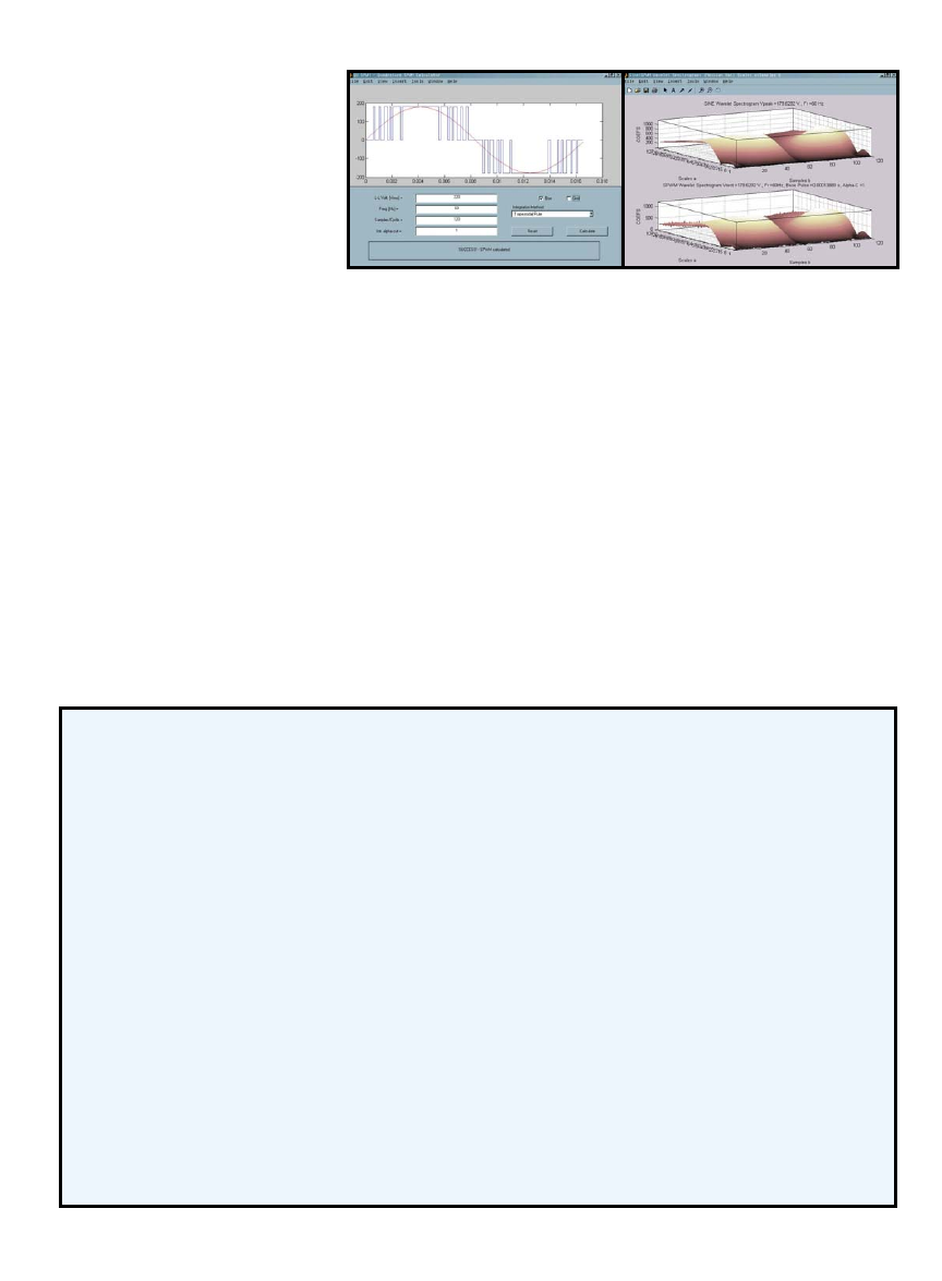
34
Issue 170 September 2004
CIRCUIT CELLAR
®
www.circuitcellar.com
CALCULATOR
MATLAB/Simulink is an excellent
platform to explore new possibilities
in electrical and electronics engineer-
ing. That’s why we chose it. The
QUSPWM calculator comprises three
files: quspwm.dll, spwm.dll, and
disc_ft.dll. disc_ft.dll is a discrete
Fourier transform special-purpose
function. spwm.dll contains the
basic algorithm shown in Figure 4.
quspwm.dll is a GUI function that
calls spwm.dll and disc_ft.dll to cal-
culate the QUSPWM and sine
quarter cycle, a reversal of the same
sequences is performed to complete
the first semicycle. Finally, the entire
cycle is complete after the data is mir-
rored with an opposite sign. This final
phase involves the generation of a
reduced-size QUSPWM array, which
presents the QUSPWM in a toggle
format. This means that commuted
or alternating values are presented
with its respective periods. This pres-
entation is useful when a look-up
table is used instead of the complete
algorithm.
chose a different approach. Using the
cosine function (with the suitable
amplitude) in the first quarter of the
cycle, we finally got a good result.
The QUSPWM basic algorithm is
depicted in Figure 4. On the right side is
a piece of code in MATLAB M lan-
guage. It’s the switched integration
operation during a quarter cycle. As we
said earlier, integration is performed
using the cosine function as a refer-
ence or modulating signal. The PWM
and cosine sequences are stored in a
reversed fashion to reflect the QUSP-
WM and the original sine reference.
Check the mapping assignation for the
spwm_complete and sine_cycle
variables in the code at the end of the
for-next iteration cycle.
An interesting and unexpected issue
arose. The cosine integral is basically a
sine wave, so the integration method
can be performed in this way. Thus,
you can easily speed up integration.
Figure 4 shows that either integration
method—the trapezoidal rule or direct
formula—can be used. Interestingly,
what isn’t shown is that the integra-
tion represents a gross low-pass filter.
After generating the basic sine and
QUSPWM sequences during the first
MATLAB/Simulink Platform
MATLAB/Simulink is a powerful algorithm simulation
environment. Using MATLAB commands and statements,
you can easily define and run algorithms, create interest-
ing GUIs, visualize numeric data in two and three dimen-
sions, and even interact with the real world using data
acquisition hardware. Simulink is an intuitive and easy-to-
use graphic block diagram simulation environment (drag
and drop). In addition, many toolboxes—ranging from
automatic control to real-time operation, COM object gen-
eration, Excel link, and C/C++ compiler—are available.
There are three interesting file formats in MATLAB.
The .mat format is basically the file format used by
MATLAB to store the workspace (constants, matrices,
structures, etc.). The .mdl file format is used by
Simulink to store the graphic workspace of a simulation.
The .m file format has two uses. It can store MATLAB
script, commands, and statements as if they were execut-
ed from its own command window. These M scripts can
manipulate variables, invoke functions, and store work-
spaces. The second use is for defining a function, request-
ing input data, and giving the output after the function
processes. By organizing data processing in functions,
you can have a better specification of your algorithm
and trace and debug errors in a more efficient way.
Defining algorithms in a function fashion with the lcc
MATLAB compiler, you can also generate MATLAB exe-
cutable file functions (known as .dll archives in Windows
platforms) and even complete stand-alone executable appli-
cations. Functions compiled as .dll archives can be invoked
and executed from the command window as any .m file.
The difference is that the .m source code can’t be seen.
Stand-alone executable applications also can be gener-
ated with the same compiler, but some characteristics
available to .m function files might not appear. These
characteristics are related to dynamic operations specific
to MATLAB and aren’t understood by the compiler.
It’s worth mentioning that you can define any other
C/C++ compiler that accomplishes this. Depending on
your needs, C or C++ code will be generated.
MATLAB can be an expensive tool (unless you have
the student version). Code in the .m file also can be port-
ed to GNU Octave with little effort. Basically, syntacti-
cal differences in commands and statements are found,
but GUI commands can’t be understood by Octave. Only
console-type applications can be ported from MATLAB to
Octave.
Photo 1a—
The GUI runs under MATLAB/Simulink with the 220-V
RMS
line voltage case at 60 Hz and 120 samples per
cycle (60 × 120 = 7,200 Hz solid state device switching frequency) under the trapezoidal rule integration method.
b—
The sine and QUSPWM wavelet spectrogram output for the QUSPWM calculator runs under the conditions depicted in
Photo 1a. Using the Mexican hat function as a mother wavelet at 128 scales, the spectrogram shows the similarities
(symmetrical lobes) and differences (rugged surface) between the original sine and the QUSPWM sequence. The
reciprocal of the base pulse value is the switching frequency of the solid-state device chosen to generate the pulses.
a)
b)
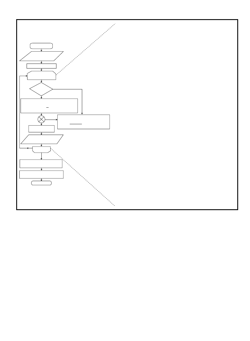
www.circuitcellar.com
CIRCUIT CELLAR
®
Issue 170 September 2004
35
sequences. You may download the files
from the Circuit Cellar ftp site.
Having placed the three files in the
same directory, select “quspwm” from
the command window to run the cal-
culator. The GUI shown in Photo 1a
will appear, running with default values.
The calculator requires four variables:
the nominal line-to-line RMS voltage,
the frequency operation, the number of
samples or pulses per cycle, and the
alpha-cut, which is an integral limiter.
The default values at the starting
time are the following: 220 V
RMS
as a
line-to-line RMS voltage, 60 Hz as the
operation frequency, 80 samples per
cycle, and one as the alpha-cut. The
operating ranges are the following:
from 210 to 480 V
RMS
for the line-to-line
voltage V
RMS
; from 1 to 60 Hz for the
operation frequency; from 80 to infinity
for samples per cycle; and above 0 to 1
for the alpha-cut. If a variable is out of
range, the calculator shows an error
message in the status window.
The results are presented in two
ways. Having calculated from
spwm.dll the basic QUSPWM and
sine sequences, quspwm.dll makes a
post-processing, generating, and stor-
ing MAT file on the hard disk with
variables containing the QUSPWM
and sine data, its frequency (magnitude
and phase) spectrum, the base pulse
width, and the three phases and line-
to-line voltages in a special MATLAB
variable structure type. The MAT file is
stored under a representative name for
easy identification. For instance, if
you typed 240 as the line-to-line volt-
age, 50 as the operation frequency, 110
as the samples per cycle, and 1 as the
alpha-cut, then the MAT file will be
named spwm_240_50_110_1.mat.
You can also present results as graph-
ic output. After storing the MAT file,
the calculator produces nine new graphic
figures on the screen. These figures show
time oscillograms, frequency spectrums,
a wavelet spectrogram, and phase and
line-to-line voltages. Some of the graph-
QUSPWM start
Initializing variables
For counter = 1
to samples/4
Integration
method
Trapezoidal rule
Direct formula
On/off pulse
QUSPWM integral
Store sine and QUSPWM in
reversed sequence
Next I
Create second semicyle sequence
for sine and QUSPWM
VL-L
FREQUENCY SAMPLES
ALPHA-CUT
Create reduced QUSPWM
sequence (toggled)
QUSPWM end
Figure 4—
As you study the QUSPWM flowchart, note how the core of the algorithm is concentrated in the first quarter of the signal period (
for
-
next
iteration cycle). It uses a cos-
inusoidal as a reference and one of two integration methods. In the final part of the
for
-
next
iteration cycle, values are assigned to the
spwm_complete
and
sine_cycle
arrays, reversing the original sequence to reconstruct the first quarter of the sine and QUSPWM data. The first semicycle sequence (sine and QUSPWM) mirrors this.
y k
amplitude
w
w
( )
×
×
(
)
=
k + 1
sin
y k
T
( )
−
(
)
×
( )
−
(
)
= y k 1 +
u k + u k 1
2
% Starting switched integration process
for counter = 1:Num_pulses_4c
% Generates cosine
k = (counter-1)*pulse_width;
% Could be u_k = As*sin((pi/2)-Ws*(k+pulse_width)) but
is simpler
u_k = As*cos(Ws*(k+pulse_width));
if (k == 0)
u_km1 = 0;
else
% u_km1 = As*sin((pi/2)-Ws*k);
u_km1 = As*cos(Ws*k);
end
% Cosenoid integration using trapezoidal rule or direct
formula
if (Int_met==1)
Integral_cosinek = Integral_cosinekm1 + (pulse_width
/2)*(u_k+u_km1);
else
Integral_cosinek=(As/Ws)*sin(Ws*(k+pulse_width));
end
if (Lock_integral_pulse==0)
% Integrals equalization by switched integration
Integral_pulsek = Integral_pulsekm1 + Tp*u_k_pulse;
end
% Integral values comparison to activate pulse integrator
if ((alpha-cut*Integral_cosinek)>=Integral_pulsek)
Lock_integral_pulse = 0;
Pulse = 1;
else
Lock_integral_pulse = 1;
Pulse = 0;
end
Integral_cosinekm1 = Integral_cosinek;
if (Lock_integral_pulse == 0)
Integral_pulsekm2 = Integral_pulsekm1;
Integral_pulsekm1 = Integral_pulsek;
end
% Assignating values first semicycle
spwm_complete(1,counter) = k;
spwm_complete(2,Num_pulses_4c-(counter-1)) = Pulse*Vcd;
sine_cycle(1,counter) = k;
sine_cycle(2,Num_pulses_4c-(counter-1)) = u_k;
end
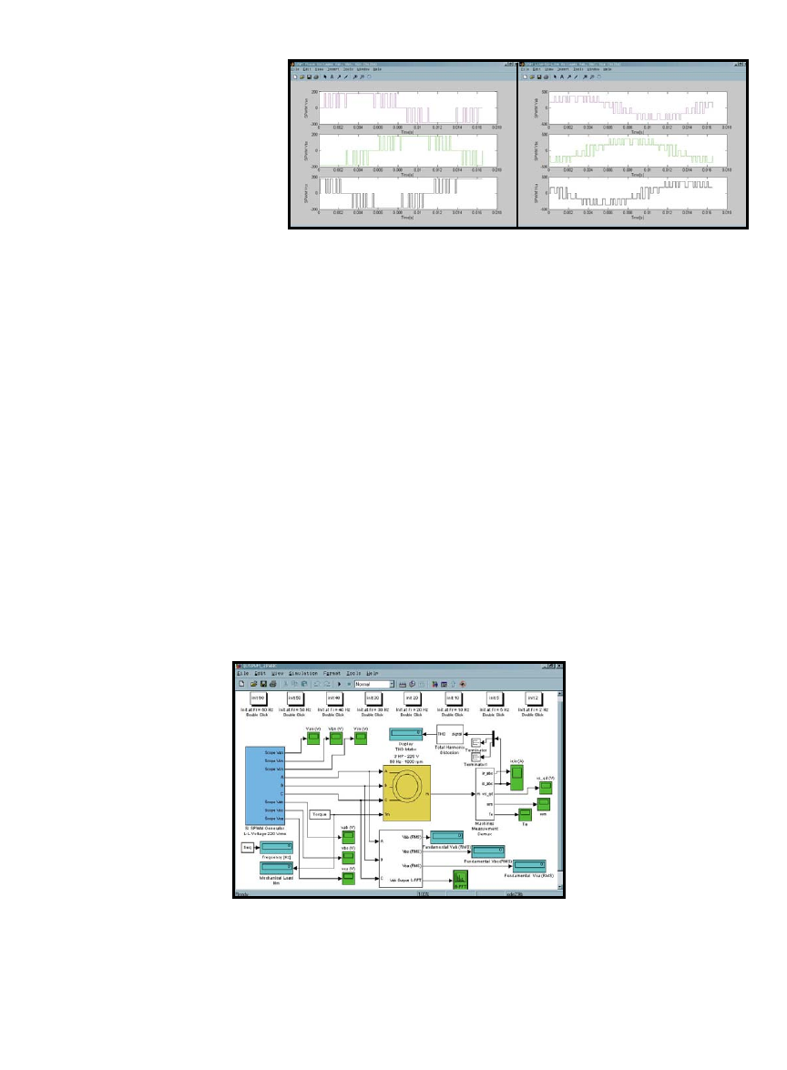
36
Issue 170 September 2004
CIRCUIT CELLAR
®
www.circuitcellar.com
tion. For each different speed, the motor
will start from a stall.
Table 1 shows the results for the
aforementioned speeds. First, notice
how the V
AB
, V
BC
, and V
CA
values indi-
cate the maintained volts-per-hertz
ratio. From 60 Hz to lower frequencies,
mechanical angular speed increases its
slippage because of the mechanical
load, which is set to 10 newton-meters
(N
⋅
m). In the two final cases (5 and
2 Hz), the mechanical load is reduced to
5 and 2.5 N
⋅
m. The slippage increases
even more, but it is normal, considering
the heavy load for low motor speeds.
The total harmonic distortion of the sta-
tor current is also mentioned in percent-
ages. Their values are basically moderat-
ics are shown in Photos 1b, 2a, and 2b.
Photo 1b shows the most striking
graphic figure of all, the wavelet spec-
trograms of the sine and QUSPWM
sequences. We used the Mexican hat
function as the wavelet’s mother.
Similarities and differences (distortions)
from both signals can be appreciated in
this way. Photo 2 also shows the phase
voltages in the positive sequence: 0°,
–120°, and 120°. You can see the line-
to-line voltages in the following
sequence: 30°, –90°, and 150°. Please
note the multistep shape of the line-to-
line voltage signals. The graphic figures
are nonregenerative, which means the
old figures remain on the screen even
if new calculations are performed.
The calculator also shows output
data in the command window. Integral
values of sine and QUSPWM are pre-
sented. This can be useful in special
cases when integral values are hard to
approximate. Running on different sam-
ples per cycle, you can also vary the
alpha-cut to get a better approximation.
The modulation index is shown on
the command window. We decided to
calculate the modulation index as the
sine area per total pulse area. Running
from the higher frequencies to the
lowest, it’s easy to appreciate how this
index is degradated.
The dll files were created with the lcc
compiler in MATLAB 6.5 in Windows
98 SE. Mathworks assures its
users that the software should
run without a problem on any
Windows 32-bit platform.
SIMULATION RESULTS
Photo 3 shows the simula-
tion scheme of an asynchro-
nous machine (squirrel-cage
rotor type) with the QUSPWM
input at different frequencies:
60, 50, 40, 30, 20, 10, 5, and
2 Hz. The motor (power block
system) has a nominal line-
to-line voltage (220 V
RMS
) and a
nominal frequency (60 Hz).
To change the speed or fre-
quency, just double-click the
desired button at the top of
Photo 3. Each button, when
double-clicked, invokes an M
script file, which loads the
variables needed for simula-
ed and they don’t increase (just at low
speeds like 5 and 2 Hz).
Finally, take a look at the switching
frequency column—samples per cycle
multiplied by operation frequency.
Ranging from 6,000 to 8,000 Hz, these
are conservative switching frequen-
cies for solid-state switching devices
(IGBTs).
We added a simulation scheme con-
taining ideal sinusoidal AC sources
with the same motor model to the
software (not shown in the figures).
Running this model, you’ll appreciate
the fact that its performance is simi-
lar to that obtained with the QUSP-
WM motor simulation, especially for
frequencies above 10 Hz. Undesired
effects, like increases in pul-
sating torque, emerge with
lower frequencies.
IMPLEMENTATION
We’ve used the QUSPWM
sequences only in a look-up
table with a basic VFD archi-
tecture. A 68HC11 micro-
controller uses this. Results
have been similar to those
observed in simulation.
We haven’t implemented
the QUSPWM as a complete
algorithm, but it wouldn’t be
too hard. The algorithm sim-
plifies even more with the
direct formula integration
method. New microntrollers
with a good cross compiler
and a fine RTOS would have
enough power to accomplish
the task.
Photo 3—
The open-loop simulation scheme of QUSPWM in MATLAB/Simulink
uses phase voltages as inputs to the squirrel cage-type, three-phase AC motor
with several cases of torque and angular speed operation. If you double-click the
buttons in the top section, variables generated with the QUSPWM calculator are
loaded in the MATLAB workspace, thus setting up conditions and parameters to
run the simulation. The green blocks are scope meters. The cyan blocks represent
meters on variables of great interest, such as fundamental values of line voltages
and the total harmonic distortion present at the stator currents of the motor.
a)
b)
Photo 2a—
Here you see the QUSPWM phase voltages in a positive sequence: 0°, –120°, and 120°. They were
obtained as output data from the calculator. The absolute value of the amplitude of the pulses is the same as what’s
indicated in Photo 1b, approximately 180 V.
b—
These are the QUSPWM line-to-line voltages in a positive
sequence: 30°, –90°, and 150° . They were obtained as output data from the calculator by using the differences of
the phase voltages shown in Photo 2a. The signals are multistep shaped and use five different values: approximate-
ly 360, 180, 0, –180, and –360 V.

www.circuitcellar.com
CIRCUIT CELLAR
®
Issue 170 September 2004
39
Armando Rosas Morato is a computer
engineer and candidate for a master’s
degree in Electrical Engineering at the
National Autonomous University of
Mexico (UNAM). He works as an elec-
tronics computer consultant. Armando’s
interests include embedded systems, soft
computing, signal analysis, and RTOS.
You may contact him at armorat@
yahoo.com or aromor@prodigy.net.mx.
Author’s Note: After a brief but fierce
struggle against cancer, Sergio E.
Elizarraras Rodriguez passed away on
July 26, 2004. He was a unique human
being and professional. His inner child
was the driving force behind many
ideas and projects, behind his deeply
humane and vivacious nature. Family
PROJECT FILES
To download the code, go to ftp.circuit
cellar.com/pub/Circuit_Cellar/2004/170.
CORRECT TECHNIQUE
The QUSPWM calculator is a soft-
ware tool programmed in MATLAB to
generate modified or special SPWM
sequences for a VFD in a three-phase
AC motor. It doesn’t make any use of a
carrier signal, just the integration oper-
ator in PWM by switched sine and
SPWM equalization areas. This makes
it a suitable technique for implemen-
tation in microcontrollers and DSPs.
The QUSPWM algorithm preserves
the fundamental value of the refer-
ence control signal and nicely attenu-
ates harmonics. Good performance
with AC motors can be observed in
terms of low-pulsating torque, low
levels of total harmonic distortion in
stator and rotor currents, and accept-
able slippages in mechanical speeds.
The software can generate oscillo-
grams and spectrums, which are use-
ful for analysis and implementation in
a look-up table sort of fashion.
I
REFERENCES
[1] S. Turkel, “Understanding Variable
Frequency Drives—Part 1,”
Electrical Construction &
Maintenance
, February 1995.
RESOURCE
P. Marchand, Graphics and GUIs with
Matlab (2nd edition)
, CRC Press, 1999.
SOURCE
MATLAB
MathWorks, Inc.
(508) 647-7000
www.mathworks.com
[2] M. H. Rashid, “Pulse-Width Modulated
Inverters,” Power Electronics:
Circuits, Devices and Applications
(3rd edition),
Prentice-Hall, 2003.
and friends will always treasure his
memory in their hearts.
God bless your soul, dear friend.
F
R
(Hz)
V
AB
(V
RMS
)
V
BC
(V
RMS
)
V
CA
(V
RMS
)
Torque (N
⋅
m)
Wm (rad/s)
% Slip
% THD steady-state stator
Switching frequency (Hz)
60
220.1
220.1
220.1
10
181.5
3.708
10.66
7,200
50
184.6
184.6
184.6
10
150.1
4.443
11.12
7,200
40
148.4
147.1
148.4
10
118.65
7.01
7.96
8,000
30
111.4
111.4
111.4
10
87.18
7.498
11.35
7,200
20
74.7
74.7
74.7
10
55.55
11.588
11.73
7,200
10
35.96
35.86
35.86
10
22.1
29.65
14.46
7,200
5
18.94
18.94
18.94
5
11.66
25.77
23
6,000
2
7.587
7.587
7.587
2.5
3.75
40.31
27.93
6,000
Table 1—
This is the response of a three-phase AC motor, with QUSPWM at different angular speed references, using the simulation shown in Photo 3. Note how the volts-
per-hertz ratio is preserved in a linear way. The fundamental values of line voltages diminish linearly as the frequency does. Harsh values are present at torque input for differ-
ent frequencies, but speed slippage (measured in percentages) performance is within the expected range, and THD values in stator currents at a steady state are kept at mod-
erate levels. Consider the conservative switching frequencies ranging from 6,000 to 8,000 Hz.
40
Issue 170 September 2004
CIRCUIT CELLAR
®
www.circuitcellar.com
O
ne of the funniest bits in Monty
Python and the Holy Grail
(1975) is
the knights’ encounter with the killer
rabbit. Well, I too have embarked on a
noble quest, however, my quest is not
for gold. I’m looking for knowledge
instead. And I’m not talking about your
everyday run-of-the-mill sort of knowl-
edge. I’m searching for 802.11b wireless
knowledge. Even though I am not out
to save the king, Camelot, and the
world from evil, my sojourn also has led
me into an encounter with a killer rab-
bit. Instead of pointy teeth, my killer
rabbit is a collection of silicon known as
the Rabbit RCM3100 RabbitCore
Module. The “killer” in my rabbit
doesn’t lie in attitude or teeth, but
rather in the application.
A standard RCM3100 prototyping
board that contains all of the expected
push button switches, LEDs, and con-
nectors supports the RCM3100
RabbitCore module. However, there is
one major difference in this spin of
the RCM3100 prototyping board: it
also carries a plug-in card that allows
for the inclusion of a wireless
CompactFlash card. In addition, the
802.11b prototyping kit comes with a
version of Dynamic C, which includes
library support for the PRISM wireless
chipset. The business end of the Wi-Fi
application kit is shown in Photo 1.
I’ve decided that this is a good time
to delve into the bitstream of Wi-Fi
communications. So, I obtained a
copy of Netasyst, which is a wireless
Sniffer package, to capture the data
that the Wi-Fi application kit’s wire-
less CompactFlash card will be throw-
those found in wired 802.3 networks.
Instead, a collision avoidance (CSMA/
CA) approach is implemented. This
means that the 802.11b device listens
to the ether before attempting to
transmit unlike 802.3 devices that col-
lide and then back off for a period of
time before trying to gain access to
the communications channel again.
To make the 802.11b CSMA/CA
scheme work, a set of timing rules is
implemented that allows an 802.11b
station to cleanly enter the communi-
cations channel, transmit its message,
and release the ether to the next
802.11b station that needs to send a
message. If an 802.11b station hears
traffic, it does not attempt a transmis-
sion and performs an exponentially
timed back-off procedure. To further
enhance data delivery reliability,
every transmitted message must be
acknowledged by the receiver.
As you well know, there are count-
less RF demons that can attack a wire-
less network. The 802.11b hardware
and IEEE standards are designed to
reduce the wireless network’s suscep-
tibility to external signals that may
compromise the network’s data.
The 802.2 LLC layer is common to
both the wired 802.3 MAC and 802.3
PHY OSI layers and the wireless
802.11 MAC and 802.11b PHY OSI
layers. This kinship in the upper OSI
layers allows the 802.11b LAN to play
easily with an 802.3 LAN at the LLC
layer and higher. This relationship is
exhibited in the Wi-Fi application kit
because a common TCP/IP library is
used to support both the wired and
Uncomplicated Wireless Networking
APPLIED PCs
by Fred Eady
ing out into the Florida room ether.
Let’s begin by attending Wi-Fi 101.
WI-FI BASICS
Wi-Fi is slang for 802.11b wireless
communications. 802.11b can be
described as a medium access control
(MAC), physical (PHY), and link layer
control (LLC) combination that oper-
ates in the unlicensed 2.4-GHz indus-
trial, scientific, medical (ISM) band at
a maximum speed of 11 Mbps. It uses
standards set forth by the IEEE.
The ISM frequency band that most
802.11b devices operate in is called
the S-Band, which extends from 2.4 to
2.5 GHz. Operation in this band puts
the typical 802.11b device at odds
with other devices (e.g., microwave
ovens) in that bandwidth. To reduce
the interference factor and raise data
delivery reliability, 802.11b devices
don’t use collision detection schemes
(carrier sense multiple access/colli-
sion detection, or CSMA/CD) like
Wireless networking is easy, as long as you have the right tools for the job. This month, Fred
shows you how to “get on the air” with Z-World’s Wi-Fi application kit, which includes a Linksys
Wi-Fi card and RCM3100 module. Go wireless in no time.
Photo 1—
The CF card’s interface is relatively simple.
The RCM3100 RabbitCore module has plenty of I/O to
support the wireless CF card and drive status LEDs
and a serial port. The Linksys wireless CF card requires
3.3 VDC, which is supplied by a switcher on the
RCM3100 prototyping board.

www.circuitcellar.com
CIRCUIT CELLAR
®
Issue 170 September 2004
41
wireless versions of RabbitCore-based
development kits.
If your wireless network includes
an access point, you’re operating in
Managed mode, or Infrastructure mode.
802.11b devices that communicate
peer-to-peer are said to be operating in
Unmanaged mode, or Ad Hoc mode.
You may see these modes described as
independent basic service set (IBSS)
for ad hoc networks or infrastructure
basic service set (BSS) for infrastruc-
ture networks. A BSS is simply a
number of 802.11b stations communi-
cating with each other using Ad Hoc
mode or Infrastructure mode. The
word infrastructure in the BSS net-
work mode description is implied and
never used in the Infrastructure mode
abbreviation for obvious reasons.
In addition to managing some of the
network traffic, access points enhance
the mobility of stations in a wireless
network. An access point usually acts
as a bridge between a wireless station
and a wired system. When multiple
access points are used in a network,
each access point must be able to pass
the mobile station’s data to and from
another mobile station, another access
point, or a wired network station. The
passing and routing of messages is per-
formed using what is called a distribu-
tion system. A distribution system in
this sense is a logical component of
802.11 that simply routes messages to
their destinations no matter which
access point in the network the
mobile 802.11b station is using.
A service set identity (SSID) and a
channel number are used to distin-
guish access points. The SSID is usu-
ally a human-readable description that
can be up to 32 characters in length.
An 802.11b station will scan the ether
channel by channel to detect an
access point to join.
In the U.S., there are 11 valid chan-
nels that can be used for 802.11b.
Most European countries can use 13
of the 14 available 802.11b channels.
If a particular SSID is specified, the
802.11b station will only join the
access point with that specific SSID.
Otherwise, the 802.11b station can be
configured to join the strongest sig-
naled access point it can find.
An 802.11b station can simply lis-
ten to the ether (passive scanning) for
a beacon from an access point or
probe it (active scanning) to detect an
in-range access point. A beacon is
transmitted by all access points and
delivers all of the information that is
necessary for an 802.11b station to
determine if it can enter a BSS via
that particular access point.
After all of the available access
points are identified by an 802.11b
station, the station can introduce
itself and join a BBS via the selected
access point. Before the 802.11b sta-
tion can participate in the BSS, the
access point must authenticate it.
There are several ways to authenticate
an 802.11b station. One method,
open-system authentication, is really
not authentication at all. The access
point simply allows the requesting
802.11b station to come in. If your
802.11b station is WEP-enabled (wired
equivalent privacy), the access point
could invoke shared-key authentica-
tion. Depending on whom you talk to,
WEP is like using a spider web to cap-
ture a Sherman tank. But using WEP
is better than using nothing at all.
You can also instruct the access
point to authenticate only certain sta-
tion MAC addresses. This authentica-
tion process is called address filtering.
It’s also possible to use the proprietary
authentication security method that the
access point vendor has implemented.
No matter how the 802.11b station
gets authenticated, after the authenti-
cation process is complete, the station
can then associate with the access
point. Association allows the 802.11b
station to use the access point to gain
access to the distribution system and
thus gain access to the network.
In an ad hoc system, each 802.11b
station that will initiate peer-to-peer
communication must be set up to the
same channel and SSID. No access
point is involved with stations config-
ured for ad hoc operation. And
because there is no access point
involved, there is no authentication or
association of the ad hoc stations.
SNIFFING AROUND
OK. Now you’ve got a general idea of
what the Wi-Fi application kit should be
doing under the covers. Unfortunately,
that’s about all I can tell you. In fact,
it’s all anyone can tell you. The inner
workings of PRISM are classified and
can be obtained only with a nondis-
closure agreement. If you’re the end
user, that’s all fine and dandy because
all you really want is to use the wire-
less device. For a developer, the minute
details must be made available so that
the desired functionality can be built
into the wireless device.
The Wi-Fi application kit is intend-
ed for wireless developers. To avoid
legal problems with the PRISM opera-
tional embargo, Z-World has wrapped
all of the secret PRISM stuff into a
driver package. The provided API
allows you, the developer, to turn
knobs inside of the wireless
CompactFlash card without exposing
Listing 1—
This is an optional step, but it sure makes life easy when you’re debugging. I opted not to use DHCP
because I wanted to be able to easily identify the Wi-Fi application kit’s wireless NIC on the wireless sniffer.
#define _PRIMARY_STATIC_IP
“192.168.0.111”
#define _PRIMARY_NETMASK
“255.255.255.0”
#ifndef MY_NAMESERVER
#define MY_NAMESERVER
“192.168.0.1”
#endif
#ifndef MY_GATEWAY
#define MY_GATEWAY
“192.168.0.1”
#endif
#if TCPCONFIG == 1
// Configuration 1: Simple static configuration of single
Ethernet interface.
#define USE_ETHERNET
1
#define IFCONFIG_ETH0 \
IFS_IPADDR,aton(_PRIMARY_STATIC_IP), \
IFS_NETMASK,aton(_PRIMARY_NETMASK), \
IFS_UP
#endif
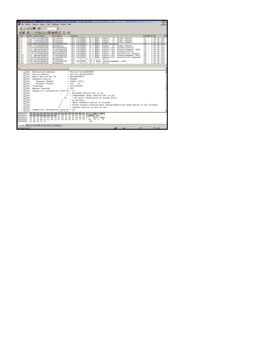
42
Issue 170 September 2004
CIRCUIT CELLAR
®
www.circuitcellar.com
the operational details of the PRISM
silicon. The Wi-Fi application kit
comes with a wireless CompactFlash
card and a set of wireless example pro-
grams that expound upon the
Dynamic C PRISM API. Before I go on
to the API, I want to show you how
easy it is to get on the air with the
Linksys wireless CompactFlash card
and the Wi-Fi application kit.
The first thing to do is define the net-
work environment in Dynamic C. The
example I used in the Florida room is
shown in Listing 1, which is an excerpt
of my modifications to the Dynamic C
TCP_CONFIG.LIB file. I’m simply giv-
ing the Wi-Fi application kit wireless
CompactFlash card a static IP address
and defining the network gateway,
which is also the access point in this
case. By doing this up front, all I had to
do was include the
#define TCPCON-
FIG 1 statement and I was covered as
far as network addressing is concerned.
DHCP operation is also an option.
To invoke it, all you have to do is
include the
#define TCPCONFIG 5
statement. Although using DHCP
makes life easy, without the pleasure
of having a wireless Sniffer it would
require me to know the Linksys
CompactFlash card’s MAC address.
Furthermore, after the wireless
CompactFlash card is authenticated
and associated, I have to access the
access point (AP) to cross reference
the wireless CompactFlash card’s
MAC address to the Wi-Fi application
kit’s newly leased IP address. To keep
wireless life as simple as possible, I
use the static IP option. The wireless
sniffer automatically associates the
wireless CompactFlash card’s MAC
and IP addresses during a sniff session.
Lots of stuff is going on behind the
simple code in Listing 2. Instead of turn-
ing on the extensive debugging that is
included in the Dynamic C wireless API
, I decided to sniff the operation to see if
I could determine what was transpiring.
The first thing you see in Photo 2 is a
probe request emanating from the
Linksys wireless CompactFlash card.
You can conclude that the Wi-Fi applica-
tion kit’s wireless CompactFlash card is
actively scanning because the Linksys
card is talking instead of listening.
The AP in the Florida room, which
is identified as “EDTP,” runs on chan-
nel 11. All APs that can hear the
Linksys wireless CompactFlash card’s
probe request must respond with a
probe response message. The sniff of
the AP’s probe response tells me that
the Florida room AP emits a beacon
every 100 time units (TUs), or every
102.4 ms. A TU is defined as a 1,024-µs
slice of time. The AP’s probe response
also tells the Linksys wireless
CompactFlash card that the AP is
capable of 11-Mbps operation. Other
fields in the AP probe response mes-
sage reveal the AP’s SSID (“EDTP”) as
well as its basic service set identifier
(BSSID), which is the AP’s MAC
address. All of this information about
the AP is also included in the beacon;
however, because the Linksys wireless
CompactFlash card is actively scan-
ning, the beacon and its information
are not used in this instance.
The authentication of the wireless
CompactFlash card is the next step.
The wireless CompactFlash card initi-
ates the authentication process with an
authentication request message that is
aimed at the EDTP AP it has just
joined. The AP acknowledges the
wireless CompactFlash card’s authen-
tication request and authenticates it.
Inside the AP’s authentication reply is a
field denoting the type of authentica-
tion. In this sniff, the open-system
authentication method was used. After
the wireless CompactFlash card sees
the status zero code in the AP’s authen-
tication reply, which means authentica-
tion was successful, it moves on to ini-
tiate an association with the EDTP AP.
The results of the wireless
CompactFlash card’s association
request include the assignment of an
association ID (AID) number and
another zero status code, which tells
the card that it is successfully associ-
ated with the EDTP AP. The least sig-
nificant 14 bits of the AID assist a sta-
tion in determining if the AP is hold-
ing buffered frames for the station.
Communication speeds, MAC
addresses, and BSSIDs are also part of
the payload in both the association
request and response messages. After
the card associated with the AP, I
could ping it from other wired hosts
and wireless stations on the network.
WIRELESS API
The seemingly automatic operation
of the wireless CompactFlash card
was actually pulled off by the default
settings inside the Dynamic C wire-
less packet driver and TCP/IP func-
tions. You can override the defaults in
your code using the Dynamic C wire-
less API. The structure of the
Photo 2—
This is a bit busy, but there’s a lot of good information in this sniff. I used the sniff information and the
Dynamic C debugging information to gain a better understanding of what the API was really doing.
www.circuitcellar.com
CIRCUIT CELLAR
®
Issue 170 September 2004
43
Dynamic C wireless API is as follows:
pd_ioctl(int nic, int cmd, char
*data, int len);
where
nic is always zero, and cmd is
the Dynamic C Wi-Fi command.
*data is the string, character array, or
pointer to a structure.
len is the size
of the data field.
To command the Linksys wireless
CompactFlash card to perform a scan,
you must issue the API call in the fol-
lowing way:
pd_ioctl(0,WIFI_SCANREQ,(char
*)0,0);
To inspect the results of the scan, all
you have to do is define a buffer
(unsigned
scanbuf[1000];) and call
the wireless API:
pd_ioctl(0,WIFI_SCANRES,(char
*)scanbuf,sizeof(scanbuf));
The wireless scan process requires
the wireless CompactFlash card’s
Roam mode be set to manual. You
also might want to force the wireless
CompactFlash card into Infrastructure
mode. Because you’re actively scanning,
the SSID should be set to “any” (any is
defined as
“ ”). These tasks are easily
performed by filling in the API blanks
in the
WIFI_INIT macro (see Listing 3).
As you can see in Listing 3, there are a
number of API commands that can be
issued in your wireless code. To set up
the Wi-Fi application kit for IBSS mode,
the Dynamic C documentation says to
code
IBBS in the parameter field of the
WIFI_MODE command. This is a typo and
the example programs will compile but
they won’t run. I checked the API source
code and the API is expecting to see
IBSS in the WIFI_MODE parameter field.
The
WIFI_OWNCHAN and
WIFI_OWNSSID API commands are
also used in Ad Hoc mode to define
the channel and SSID of the independ-
ent station. I installed a second AP
called
CircuitCellar in a remote
part of the Florida room and forced the
Linksys wireless CompactFlash card
to associate with it by coding
CircuitCellar in the parameter
field of the
WIFI_SSID command.
WEP is enabled by coding:
pd_ioctl(0,WIFI_WEP_FLAG,”1”,
0);.
Listing 2—
The Dynamic C programmers have gone way out there to make wireless networking with a Rabbit
dead easy. Note the
TCPCONFIG 1
definition. It tells the compiler to use my modified copy of the
TCP_CONFIG.LIB file.
#define TCPCONFIG 1
#define PKTDRV
“cfprism.lib” // Bring in the cfprism.lib
#use dcrtcp.lib // Bring in TCP functions
void main()
{
sock_init();
while(1){tcp_tick(NULL);}
}
Listing 3—
If this macro is not defined in the main program, a default WIFI_INIT is executed. What it boils
down to is that this macro and its parameters are all you need to know about to go wireless with a Rabbit.
#define WIFI_INIT
\
pd_ioctl(0,WIFI_MODE,”BSS”,0);
\
pd_ioctl(0,WIFI_SSID,””,0);
\
pd_ioctl(0,WIFI_OWNCHAN,””,0);
\
pd_ioctl(0,WIFI_OWNSSID,””,0);
\
pd_ioctl(0,WIFI_WEP_FLAG,””,0);
\
pd_ioctl(0,WIFI_WEP_AUTH,””,0);
\
pd_ioctl(0,WIFI_WEP_USEKEY,””,0);
\
pd_ioctl(0,WIFI_WEP_KEY0,””,0);
\
pd_ioctl(0,WIFI_WEP_KEY1,””,0);
\
pd_ioctl(0,WIFI_WEP_KEY2,””,0);
\
pd_ioctl(0,WIFI_WEP_KEY3,””,0);
\
pd_ioctl(0,WIFI_ROAM,”manual”,0);
\
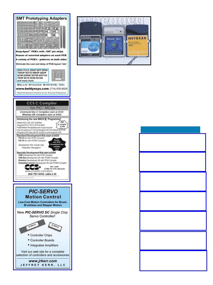
44
Issue 170 September 2004
CIRCUIT CELLAR
®
www.circuitcellar.com
Four sets of 13 bytes form the WEP
keys. The transmit key is selected
using the
WIFI_WEP_USEKEY com-
mand. Private authentication is acti-
vated with the
WIFI_WEP_AUTH com-
mand and a
1 in the parameter field.
There’s one more API command
that allows the wireless programmer
to start and stop the MAC.
pd_ioctl
(0,WIFI_MAC,”off”,0); disables
the wireless CompactFlash card’s MAC
engine and
pd_ioctl(0,WIFI_MAC,
”on”,0); enables the MAC. This
command is useful when you want to
programmatically change the wireless
CompactFlash card’s configuration.
Stop the MAC to make your changes.
GETTING SERIOUS
The Wi-Fi application kit is not for the
meek and mild. If you’re new to wireless
networking, be prepared to do lots of
reading as you experiment with your kit.
The debugging capabilities of Dynamic
C are, as my kids would say, “off the
chain.” However, if you can’t relate what
you see in the debugger session to the
802.11b standard, you’re not going to be
able to understand what’s really going on
with the wireless CompactFlash card,
and you most likely won’t be successful
with your own design. That’s why I
decided to bite the bullet and obtain
the wireless sniffer. With it, I can tie all
of the wireless acronyms (AID, BSSID,
SSID, etc.) to a piece of real data inside
a captured wireless 802.11b frame.
After becoming comfortable with
802.11b and the kit, I wanted to
explore the differences in wireless
CompactFlash cards. So, I browsed the
list of compatible wireless cards that
Fred Eady has more than 20 years of
experience as a systems engineer. He has
worked with computers and communi-
cation systems large and small, simple
and complex. His forte is embedded-sys-
tems design and communications. Fred
may be reached at fred@edtp.com.
SOURCES
D-Link Air Wireless CompactFlash card
D-Link Systems, Inc.
(800) 326-1688
www.dlink.com
WCF12 Wireless CompactFlash card
Linksys
(800) 326-7114
www.linksys.com
MA701 Wireless CompactFlash card
Netgear
(888) 638-4327
www.netgear.com
Netasyst network analyzer
Network Associates
(800) 338-8754
www.nai.com
RCM3100 RabbitCore
RabbitSemiconductor
(530) 757-8400
www.rabbitsemiconductor.com
TEW-222CF Wireless CompactFlash card
TRENDnet
(310) 891-1100
www.trendware.com
Wi-Fi application kit
Z-World
(530) 757-3737
www.zworld.com
comes with the kit and pur-
chased a few of them (see
Photo 3). They all worked as
designed with no apparent
differences in operation.
The folks at Z-World are
famous for producing prod-
ucts that are running before
you even open the box. The
Wi-Fi application kit is no
exception. It proves that
embedded devices do not
have to be complicated to be
wireless.
I
Photo 3—
You can read about how things work until the cows come
home. However, sometimes it’s just better to get your hands dirty
and discover things yourself. The Z-World folks (Ingo Cyliax includ-
ed) tested these cards, and I decided I would too.
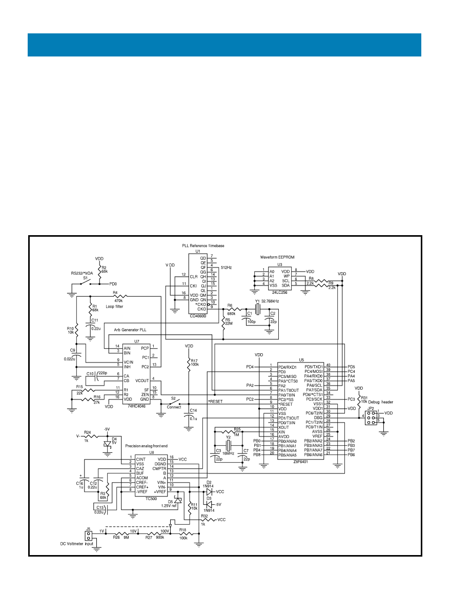
of the two on-board UARTs. These
aren’t common functions on most
MCUs, but I knew they would be sig-
46
Issue 170 September 2004
CIRCUIT CELLAR
®
www.circuitcellar.com
T
wo things struck me as interesting
when I first looked over the documen-
tation that came with the Z8 Encore!
Multilab
Brian’s Multilab is comprised of an arbitrary function generator, a digital pulse generator, and
more. Read on to learn how he built this multipurpose test instrument.
development kit: the three-channel
DMA controller and the IrDA
encoder/decoders associated with each
FEATURE ARTICLE
by Brian Millier
Figure 1—
Along with the Z8 Encore! MCU, most of the arb function generator’s circuitry is contained here. The DC voltmeter circuit is also included.
Build a Z8 Encore!-Based Multipurpose Test Instrument
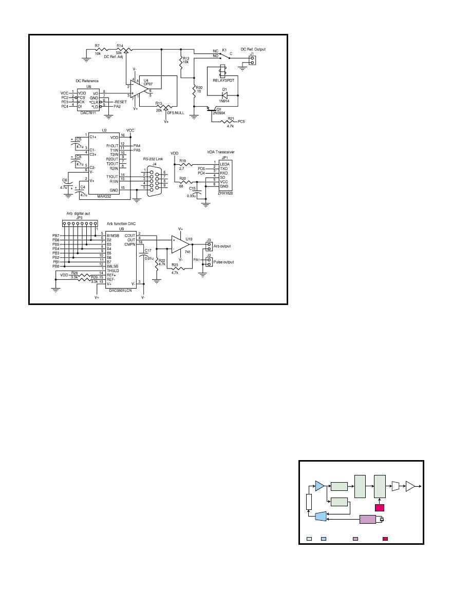
www.circuitcellar.com
CIRCUIT CELLAR
®
Issue 170 September 2004
47
I often use all of an MCU’s I/O pins
in a design, so having the program-
ming/debug functions all handled by
only one dedicated MCU pin seemed
like a great idea. In the following sec-
tions, I’ll describe the hardware and
software aspects of the project.
DESIGNING THE ARB
A block diagram for a basic arbitrary
function generator is shown in Figure 3.
The address counter accesses the
waveform memory sequentially, and
the data in the waveform memory
array is fed to an 8-bit DAC. The
DAC0801LCN is a current-mode
DAC. An op-amp converts this into
the required output voltage waveform.
To generate a waveform of a desired
frequency, the address counter must be
incremented at this frequency multi-
plied by the depth of the waveform
memory array. The depth of the array
represents the number of data points
used to make up one complete cycle of
the output waveform. So, the greater
the depth, the more accurately one can
simulate a particular waveform. For
simple waveforms such as square waves
and triangle waves, this isn’t too criti-
cal. But, it’s obvious that to generate
complex waveforms, the depth of the
memory array must be commensurate
with the complexity of the waveform.
To achieve adequate frequency reso-
lution, the clock, which increments
the address counter, must be tuneable
in reasonably fine steps. So, for exam-
ple, achieving a 1-Hz output wave-
form resolution with a waveform
depth of 256 data points requires the
clock be tuneable in 256-Hz amounts.
There are basically two ways to
approach this. You can start with an
extremely high-frequency quartz crys-
nificantly beneficial for a project I had
in mind.
I wasn’t totally surprised to see the
triple-DMA controller. Back in the
1970s when Intel started the PC revolu-
tion with the 8080 microprocessor,
Zilog wasn’t far behind with a compati-
ble device, the Z80. It took over much
of Intel’s early market share largely
because it contained an on-board
refresh counter, which made it easy to
use inexpensive dynamic RAM chips.
The project I had in mind consisted of
a multipurpose lab instrument comprised
of an arbitrary function generator, a digi-
tal pulse generator, a high-resolution DC
voltmeter, and a DC reference source. To
keep the unit compact and inexpensive, I
wanted to eliminate the conventional
front panel and use a Palm Pilot PDA to
handle that function. The Z8 Encore!’s
DMA channels are ideal for the arb
function, and the IrDA encoder/decoder
block makes implementing the IR link
to the Palm Pilot easier.
After using flash memory MCUs for
several years, I’m now spoiled. Happily,
the Z8 Encore! family comes with up to
64 KB of flash memory. The arb genera-
tor function needs a significant amount
of waveform memory, and the 4-KB
RAM included in the Z8 Encore! fits
the bill nicely (see Figures 1 and 2).
Although I’ve used numerous 8-bit
MCUs over the years, I had not tried
any Intel 8051-derived MCUs or Zilog
MCUs. The combination of a good
development board, stable IDE software,
and the on-chip debug facility made the
transition relatively painless, I must say.
I’m particularly impressed by the on-
chip debug/programming facility.
Basically, using a single-pin, half-duplex
serial link to the MCU, it manages to
program the flash memory quickly.
Furthermore, it allows for the complete
in-circuit debugging of your program,
including register/memory contents
and port status, as well as the symbol-
ic readout of your C program variables.
Figure 2—
Here you can see several mixed-signal components associated with the Multilab, as well as both the
IrDA and RS-232 interface circuits.
VCO
Timer2
÷N
÷N
Address
counter
Waveform
memory
DAC Amplifier
Waveform load
Timer0
÷64
32.768 kHz
Loop filter
Phase
detector
512 Hz
Z8
74HC4046
MC14060
Z8 Firmware
Figure 3—
As you study the different sections of the
arbitrary function generator, keep in mind that the
green blocks are handled by the Z8 Encore!.

48
Issue 170 September 2004
CIRCUIT CELLAR
®
www.circuitcellar.com
grammable divider, and triggers DMA0
at the desired rate.
The DMA controllers contain regis-
ters for RAM start and end addresses,
so it is easy to program in the desired
waveform depth by setting the RAM
ending location accordingly. The Z8
Encore! contains 4 KB of RAM, which
is more than enough to handle the
waveform depths that I need.
The DMA controller can operate in
Single Block or Repetitive mode. At
this stage, my design is set up to pro-
duce repetitive waveforms, but chang-
ing this mode bit, and using an external
trigger to initiate the generation of a
one-shot wave output, can change this.
When the Z8 Encore!’s timers are
clocked from an external source, as is
the case with Timer2, the maximum
clock rate is the system clock divided
by four. I run the Z8 Encore! at 16 MHz,
which is convenient for the pulse gen-
erator function, so the maximum VCO
frequency shouldn’t exceed 4 MHz. I
chose the VCO’s RC tuning compo-
nents to produce frequencies in the 1-
to 3-MHz range, which is safely under
the 4-MHz limit. Timer2 divides the
VCO frequency by N, so its output fre-
quency range can go up to 1.5 MHz.
The Z8 Encore! datasheet does not
specify how fast the DMA channels
can operate. Because the DMA con-
troller must steal the bus from the
MCU to do the transfers, this timing
will vary somewhat depending on
which instructions the MCU is per-
forming. With my code, I found that
the DMA controller could be counted
on to transfer data up to about a 2-MHz
rate, so the 1.5-MHz maximum fre-
quency output of Timer2 is OK.
To phase-lock the VCO at the
necessary frequency in the 1- to
3-MHz range, its output must be
divided down to the PLL’s 512-Hz
reference frequency (provided by
the MC14060 oscillator/divider
chip). The Z8 Encore!’s Timer0
performs this task. I chose 512 Hz
because it provides adequate out-
put frequency resolution and isn’t
so low as to be slow phase locking.
Table 1 shows the waveform
depth and resolution for the vari-
ous frequency ranges. The higher
frequencies must use a smaller
tal oscillator (50 to 100 MHz) and use
a variable modulus divider chip to pro-
duce a clock signal in the desired
range. This approach can yield a rea-
sonable resolution, but the resolution
will vary throughout any given range.
A better approach is to use a PLL (i.e.,
a VCO that’s phase-locked to a refer-
ence signal). The reference frequency
is set equal to the desired frequency
resolution multiplied by the waveform
memory array depth. The VCO can be
fine-tuned over an octave (or greater)
frequency range, and Timer2 in the Z8
Encore! can divide this down to the
correct frequency needed to clock the
waveform memory at the correct rate.
I chose the latter option (see Figure 3).
My goal was to use the Z8 Encore! for
as much of the circuit as possible. All I
really needed to add externally were a
CMOS 74HC4046 VCO/phase detector
chip and the DAC/output buffer. To gen-
erate a reference signal for the PLL, I
could’ve used Timer1 in the Z8 Encore!.
However, I allocated Timer1 to handle
the timing for the DC voltmeter func-
tion to this project. Therefore, I used an
MC14060 CMOS oscillator/divider chip
and a 32,768-Hz watch crystal to pro-
vide the 512-Hz reference for the PLL.
The DMA function in the device is
essential to make the Z8 Encore! func-
tion as an arb. The Z8 Encore! con-
tains three DMA channels, one of
which is dedicated to the ADC. The
other two channels can be independent-
ly programmed to transfer data in or out
of the Z8 Encore! RAM to any Z8
Encore! port that you select.
I connected the DAC to port B, so
that is the destination register that I
programmed into DMA0. Any of the
Z8 Encore!’s timer outputs can be
used to trigger this data transfer at the
desired rate. As you can see in Figure
3, the VCO output is fed into the Z8
Encore!’s Timer2, which acts as a pro-
waveform depth because the maxi-
mum waveform memory clock rate is
about 1.5 MHz, as outlined previously.
With a fixed 512-Hz PLL reference fre-
quency, as the waveform depth
becomes smaller, the resolution also
decreases but it is still reasonable.
The arb generator works in two
modes. For common waveforms—such
as sine, triangle, sawtooth, and
square—the Z8 firmware calculates
the waveforms, using the C library’s
floating point routines, and loads
them into RAM as needed. For any
other waveform (i.e., arbitrary), the
RAM is loaded with values that have
been previously saved in a 24LC256
I
2
C flash memory chip.
For simplicity, I broke the 32-KB flash
memory space into 1-KB segments,
allowing one to store up to 32 arbitrary
waveforms with a depth of 1,024 (or
less). Generating and downloading these
waveforms are the only functions per-
formed without the Palm Pilot. Rather,
they’re accomplished using a PC applica-
tion, which also can act as the device’s
front panel in lieu of the Palm Pilot.
There is nothing written in stone that
says the output of the arb waveform
memory must be limited to setting a
DAC and thus producing an analog
waveform. I added an eight-pin header to
the board wired up to the eight data
input lines of the DAC. By loading an
arb waveform with the proper digital val-
ues, it’s possible to tap into these lines
and get up to eight synchronized digital
signals (of a repetitive nature). Along
with the various analog waveforms like
sine and triangle, the firmware also gen-
erates several stepper motor phase
sequences that can be selected.
Frequency Waveform
Resolution
range
depth
(hertz)
0.06–5000 Hz
256
2
5–10 kHz
128
4
10–20 kHz
64
8
20–40 kHz
32
16
Table 1—
Although both the waveform depth and fre-
quency resolution drop as the frequency increases, it’s
adequate for many low-frequency and audio applications.
Prescaler Minimum/maximum Resolution
ratio
period
(microseconds)
128
16 µs–0.52428 s
8
64
8 µs–262 ms
4
32
4 µs–131 ms
2
16
2 µs–65,535 µs
1
8
1 µs–32,767 µs
0.50
4
0.5 µs–16,383 µs
0.25
2
0.25 µs–8,192 µs
0.125
1
0.125 µs–4,095 µs
0.0625
Table 2—
The pulse generator is based on 16-bit counters
coupled with prescalers. Although it can produce a wide
range of pulses, its resolution is basically limited by the reso-
lution of these 16-bit counters.
www.circuitcellar.com
CIRCUIT CELLAR
®
Issue 170 September 2004
49
I was tempted to use the Z8 Encore!
development board, with its on-board
Z8F6403, for this project. This Z8
device, which contains four timers,
would have eliminated the MC14060
circuitry that I used for the PLL refer-
ence clock. It would have also provid-
ed more versatility. However, I decid-
ed to save the development board for
future development work and instead
use one of the Z8F6401 (40-pin DIP)
chips included in the kit.
PULSE GENERATOR
The Z8 Encore!’s timers are
extremely versatile (including a PWM
function), so I decided to include pulse
generation capability in the design.
The only additional thing required
was a bit more firmware. All of the
hardware was already there.
The 16-MHz system clock acts as
the timing reference, giving a resolu-
tion of 0.0625 µs on the fastest range.
Both the pulse period and pulse width
are entered as 16-bit values, giving a
wide timing range. Using the Timer0
prescaler, with its division rates from
two through 128, you can extend the
range from microseconds to seconds,
as shown in Table 2.
When in use, merely enter the peri-
od and width values, using the appro-
priate units (seconds, milliseconds,
and microseconds), and the firmware
picks out the correct range and sets
the prescaler accordingly. The Z8
Encore! PWM function can produce
either active-low or active-high pulses.
So far, I have only allowed for active-
high pulses in the firmware.
HIGH-RES DC VOLTMETER
Another feature I thought would be
useful in the MultiLab is a high-reso-
lution DC voltmeter. The timers and
display were already there, so
all I had to add was a suitable
A/D converter. For high-reso-
lution use, it’s hard to beat
the tried-and-true dual-slope
integration method, which is
what is used in most DVMs.
In the past I’ve successfully
used the ICL7135, but
Microchip now makes the
TC500, which is a higher res-
olution (16-bit) analog front-
end device. The TC500 is small, inex-
pensive, and somewhat more suited
to this application.
The TC500 is basically a precision
bipolar dual-slope integration A/D
converter with a built-in auto-zero
function. All you have to add to com-
plete the design are three capacitors
and a stable voltage reference. The
MCU must provide two digital I/O
signals (control A, B) to control the
four-phase conversion sequence that
the device uses. Also, the MCU must
accurately time both the integration
and deintegration phases and monitor
the state of the TC500’s comparator
during the former phase. I used the Z8
Encore!’s Timer1 to handle the tim-
ing. I also used two other I/O lines for
the control and comparator monitor-
ing function. To provide for good
power line noise rejection, the inte-
gration phase is set to 16 power line
cycles, or 266.66 ms.
Figure 4 is a timing diagram for the
circuit. To match common DVMs, I
used a 10-M
Ω
input divider chain and
implemented three input ranges: 1,
10, and 100 V. The voltmeter circuitry
is shown in Figure 1.
DC VOLTAGE REFERENCE
I often need an accurate DC voltage
reference source. Generally, this is in
the 0- to 10-V range, but I occasion-
ally need to simulate a thermocou-
ple that produces signals in the low
millivolts range.
I chose a Burr-Brown 12-bit SPI
DAC to provide this voltage reference
source. The DAC7611 comes in an
eight-pin DIP and contains its own
voltage reference. I added an op-amp
output buffer and a 1000:1 voltage
divider to provide for 0- to 10-V and
0- to 10-mV output ranges.
300 ms
266 ms
Variable
131 ms
Control A
Control B
Auto zero
Integrate
Deintegrate
Integrator
output zero
Figure 4—
This is a conversion timing diagram for the TC500 ana-
log front-end device. I chose an integration time of 16 PLCs to min-
imize the 60-Hz noise pick-up.
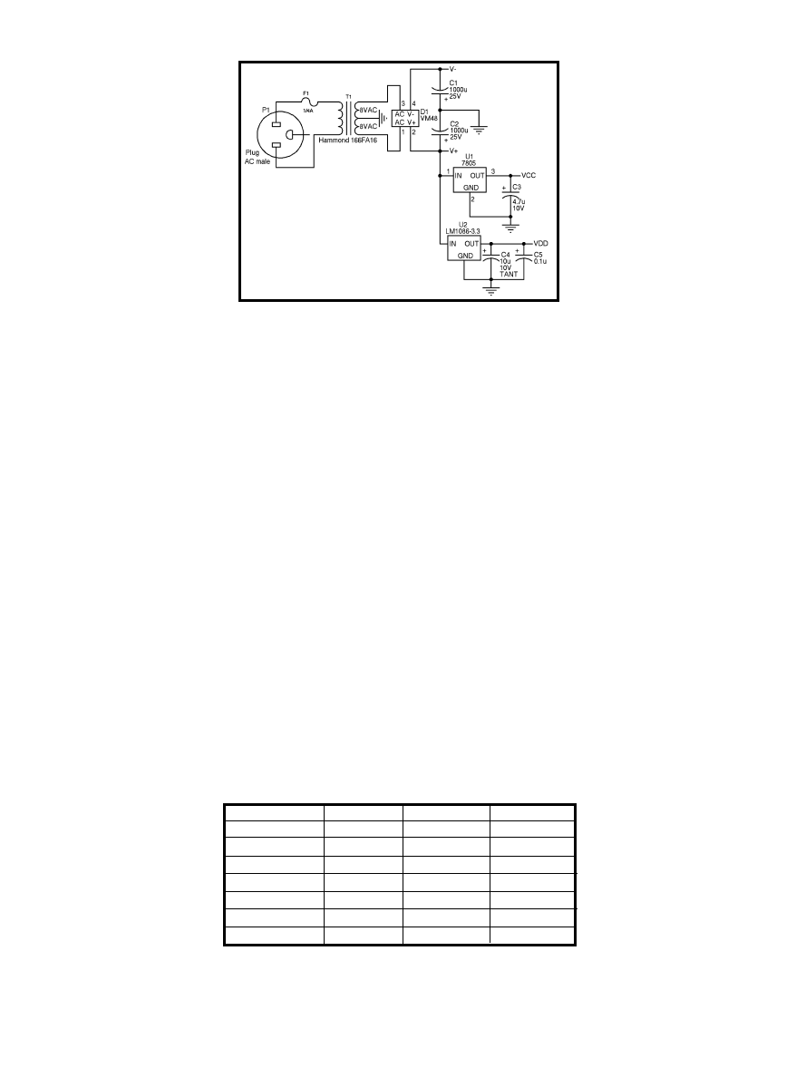
50
Issue 170 September 2004
CIRCUIT CELLAR
®
www.circuitcellar.com
col to the IrDA protocol, all you need
to do is set the U1CTL1 register’s bit 0
to 1. The only hardware needed is the
IrDA transceiver module, which con-
tains both the IR LED/driver and
detector/amplifier. During early tests,
I was impressed with the operation of
the Zilog IrDA transceiver module
contained on the evaluation board, so I
used a similar ZHX1820 transceiver
module for this project.
The circuitry only handles the phys-
ical layer of the communications link.
There is an extremely sophisticated
(meaning lots of code!) protocol called
irCOMM that PDAs, laptops, and print-
ers use to communicate with each other
in a wireless fashion. It handles all of the
nitty-gritty details of networking these
devices together in an error-free way.
The Palm Pilot includes all of the
drivers for the protocol in its operating
system. I did not come across an
irCOMM protocol stack for the Z8 in
the C libraries I had. When I looked at
the protocol’s details, I decided
it was much too complex for
my application.
IR communication has
some parallels in RF commu-
nication. Stray noise found in
RF is replaced with stray
light. In both cases the dis-
tance between the transmit-
ter and receiver may cause
the received signal strength
to vary over a wide range.
The IrDA transceiver mod-
ules do all they can to com-
bat this. The IR LED is
pulsed fairly hard to produce
a strong IR light signal, and
an AGC-controlled amplifier
follows the photodector to
even out the differences in received
signal strength.
In my experiments with a Palm
Pilot and the Z8 Encore! development
board, I found only a few things that
you need to worry about when trying
to achieve error-free data transfers
between the two devices. First, note
that you have to keep the two devices
pointed at each other at a distance of
less than one yard. Second, allow a
fraction of a second of dead time
between transmitting and receiving
data because the IrDA link is only a
half-duplex link. Third, send a short
preamble before the actual message
because the IrDA receiver operates
using AGC. The preamble gives the
receiver time to adjust from a state in
which it looks (in a sensitive way) at
stray light to a state in which its gain
has been adjusted to match the level
of the incoming IR signal. I chose a 10-
character preamble of 0xFF bytes before
the actual message. As a result, the
byte pattern sends one
short start pulse per charac-
ter (the start bit) with
which the receiving UART
easily synchronizes.
Finally, frame the mes-
sage to start with a start-
of-text control character
and end with an end-of-
text control character.
This allows the receiving
end to easily identify the
actual message. Using this
simple scheme, it’s easy
IRDA AND RS-232 LINKS
The design of the IrDA link
to the Palm Pilot is simple,
thanks to Zilog. The Z8
Encore! contains two UARTs,
each of which includes a com-
plete IrDA encoder-decoder,
or ENDEC. The IrDA physical
layer encoding/decoding isn’t
a complicated process. The
data format is basically the
same asynchronous format
used for RS-232 serial com-
munications, except that
instead of using two different
voltage levels to represent
ones and zeros, the IrDA for-
mat uses a short pulse within
the bit cell time to indicate a
zero and the lack of a pulse to indicate
a one.
In asynchronous data protocol, all
characters start with a 0 start bit;
therefore, all IrDA characters start
with a short pulse representing this
start bit. This forms the timing refer-
ence needed to recover the following
8 data bits, as well as the stop bit at
the end, which is a one.
The pulse width used by IrDA is
defined as one-sixteenth of the bit cell
time (the reciprocal of the data rate).
It’s the timing of this pulse width that
creates a bit of a problem. In an MCU
that contains just a standard UART
function, adding the ENDEC function
outside the MCU can be done using
specialty chips designed for this pur-
pose, like the Texas Instruments
TIR1000 and Unitrode UCC5343.
However, these devices require a tim-
ing reference at 16 times the data rate
used by the MCU’s UART.
This timing signal, although defi-
nitely present within the
MCU’s UART block, is
generally not brought out
to any of the MCU’s port
pins. Therefore, it has to be
provided for in some other
way. That’s why the
ENDECs contained within
the Z8 Encore! are so
handy.
I used the Z8 Encore!’s
UART1 for the IrDA port.
To switch from normal
asynchronous data proto-
Command number
Description
Parameter #1
Parameter #2
1
Pulse generator
Period
Pulse width
2
Wave generator
Frequency
Wave type
3
Stepper drive
Step rate
Sequence type
4
Store arb wave
Waveform number
Waveform depth
5
Select arb wave
Waveform #
“0” (not used)
6
DC voltmeter
“0” (not used)
“0” (not used)
7
DC reference
Voltage
Range (V or mV)
Table 3—
The MultiLab accepts seven commands. Most commands require two parame-
ters, except the DC voltmeter, which expects no parameters but returns a voltage
instead. Although it is not shown here, the fourth command also requires the actual
waveform array to be sent after the two parameters shown.
Figure 5—
A multivoltage power supply is needed because this is a mixed-signal
design. A Zener diode provides an additional –5-V supply, which isn’t shown
here (refer to Figure 1).
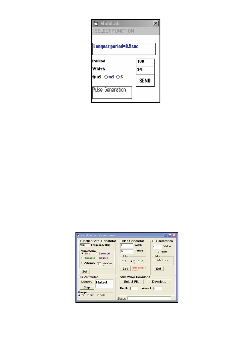
www.circuitcellar.com
CIRCUIT CELLAR
®
Issue 170 September 2004
51
to transmit data back and forth
between this design and the Palm
Pilot that controls it.
I used UART0, along with a
MAX232 for level shifting, for the RS-
232 link to the PC. Although the pre-
amble and message protocol used for
the IrDA link isn’t necessary for this
direct-wired link, I used it here as well
to simplify the program.
Fortunately, the MobileVB software
I used to write the Palm Pilot applica-
tion supports both RS-232 and IrDA
communications links. It also provides
for both raw, which I used, and
irCOMM protocols for the IrDA link.
POWER SUPPLY
Figure 5 is the schematic diagram of
the power supply. Because of the
mixed-signal nature of the project, a
number of voltages were necessary.
Both the arb DAC and the op-amps are
connected to the raw
±
12-V outputs of
the bridge rectified power supply. The
Z8 Encore! and IrDA transceiver need
3.3 V, which I also used for the CMOS
chips in the PLL and the 24LC256
flash memory. An LM1086-3.3 pro-
vides the 3.3-V supply.
However, the MAX232, DAC7611,
and TC500 need 5 V, so a 7805 is also
required. The TC500 also needs a nega-
tive voltage source, which is provided by
a 5-V Zener diode. Maxim also makes
the TC510 with a built-in charge-pump,
but I didn’t spring for this version
because I had a negative supply available.
Z8 FIRMWARE
I’d used either assembly
language or BASIC for every
MCU I’ve worked with over
the years. I hadn’t used C lan-
guage. Because the Z8 Encore!’s
IDE and on-chip debug facility
were tailored to work with the
free ANSI C compiler included
with the development kit, I
decided it was time to learn
something new.
I used the serial I/O, I
2
C,
SPI, and floating point/
trigonometric functions
included with the C compiler
package. There is also a
library titled API, which han-
dles all of the timer functions. I
used it to some extent, but in some
places, particularly where setting up
the timers needed to be done quickly, I
wrote my own faster timer handling
routines.
I used numerous variables, including
a memory array of 256 or more ele-
ments for the arb waveform memory,
so I implemented the large memory
model in the compiler. The small
memory model uses only the basic
256-byte register space in the Z8
Encore!. I also had to remember to
explicitly instruct the compiler to use
the floating-point library because the
waveform generation, as well as many
of the timing calculations, was done
in floating point. The program used up
approximately 60% of the 64-KB flash
memory in the Z8F6401.
The program flow is fairly basic. At
reset, all of the necessary I/O ports are
configured properly. Then the RS-
232/IrDA switch is checked to see if
the unit is going to be talking to a PC
directly or to a Palm Pilot via the
IrDA link. The applicable UART port
is then selected as the active commu-
nication port, and the program enters
a loop awaiting commands.
All commands consist of a single
line of ASCII text containing three
numeric parameters. The first parame-
ter is the function number (currently
one through seven). The meaning of
the other two parameters varies by
function. The only exception is the
store waveform command. After the
normal command line, a series of
bytes follows. These are the waveform
values themselves.
After the Z8 has received a com-
plete line, it uses the
sscanf function
to parse it into the three numeric
parameters. The first parameter is
used with the switch function to call
the appropriate routine. The other two
parameters, which are floating-point
numbers, are used to set up the wave-
form shape, frequency, pulse widths,
and reference voltage as required by
that particular function. Only in the
case of the DC voltmeter function is
a value returned to the PC or Palm
Pilot. In this case, a 16-bit integer is
transmitted back to the host where it
is scaled into the correct voltage
readout. Table 3 shows the structure
of the various commands used by the
MultiLab.
PC & PALM APPS
Both Palm Pilot and PC
applications are needed to
operate the MultiLab. In the
case of the Palm Pilot, I
used AppForge’s MobileVB
program, which is designed
as an add-in tool for Visual
Basic 6, and allows the
Visual Basic programmer to
operate in the familiar
Visual Basic environment.
However, it creates a pro-
gram that will run on the
Palm Pilot.
I have experience with
Visual Basic, so MobileVB
Photo 1—
The Palm Pilot application program is shown
here running under PC emulation. My digital camera
didn’t take a clear photograph of the Palm’s small screen.
Photo 2—
The Visual Basic PC application acts as the MultiLab’s front panel.
Although it handles the same functions as the Palm Pilot application, it’s easier to
use because it isn’t limited by the Palm Pilot’s small screen limitations.
52
Issue 170 September 2004
CIRCUIT CELLAR
®
www.circuitcellar.com
the project has met my expectations.
I
Editor’s Note: Brian’s Multilab project
won First Prize in the 2003 Flash for
Cash Z8 Encore! International Design
Contest. For more information, go to
www.jandspromotions.com/zilog2003.
PROJECT FILES
To download the code, go to ftp.circuit
cellar.com/pub/Circuit_Cellar/2004/170.
SOURCES
MobileVB Program
AppForge, Inc.
TC500CPE Analog front end
Microchip Technology, Inc.
www.microchip.com
LM1086 Regulator
National Semiconductor Corp.
www.national.com
3052 DPO Oscilloscope
Tektronix, Inc.
www.tek.com
Z8 Encore! microcontroller, IrDA
transceiver
Zilog, Inc.
www.zilog.com
wasn’t too hard to
get used to. I wrote
an application to
handle the various
functions, but, given
the time constraints of
the Zilog Flash for
Cash Z8 Encore!
International Design
Contest, it isn’t too
fancy. Photo 1 shows
one screen of the
Palm application run-
ning in MobileVB’s PC
Emulation mode.
However, my digital
camera couldn’t take a
clear enough picture
of the application running on the Palm
Pilot to show you.
The PC application, which was
written in Visual Basic 6, performs a
similar function to the Palm Pilot pro-
gram, except it can also download arb
waveforms to MultiLab. Photo 2 is a
screen shot of the application. Photo 3
shows a sampling of some of the arb’s
output waveforms. Photo 4 shows the
MultiLab without its top cover.
BUILT-IN ADVANTAGE
Considering that the Z8 Encore! and C
language were completely new to me, I
must admit that working with the Z8
development board and software was a
pleasure. During the early stages of the
project as I stumbled around with unfa-
miliar C syntax, the on-chip debugger
was a prayer answered. The MCUs I’ve
used in past projects didn’t have this
built-in function, but now I don’t want to
do without it. Overall, I’m pleased that
Brian Millier is an instrumentation
engineer in the Chemistry Department
at Dalhousie University in Halifax,
Canada. He also runs Computer
Interface Consultants. You may reach
him at brian.millier@dal.ca.
Photo 4—
Apart from the power supply, all of the
MultiLab’s circuitry fits easily on a vector 8001 proto-
type card. The window that allows IR communication
with the Palm Pilot is barely visible under the red-han-
dled power switch.
Photo 3—
Here are four output signals from the MultiLab captured by my Tektronix
3052 DPO oscilloscope. Working clockwise from the upper left you can see a sine
wave with added harmonics, pure sine wave, square wave, and sawtooth.

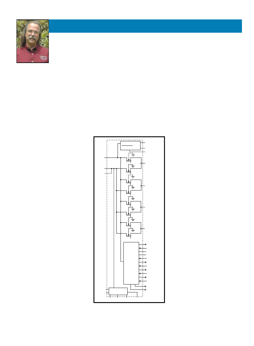
54
Issue 170 September 2004
CIRCUIT CELLAR
®
www.circuitcellar.com
R
ecently, I was searching through an
old file cabinet for some paperwork that
came with my Toshiba laptop. I was try-
ing to put its age into context with the
introduction of USB. The user’s manual
(remember when they came printed?) was
copyrighted in 1997. I’m talking about an
environmentally friendly one here. It was
printed in the U.S. on recycled paper with
soy ink. I found a special one-sheet
inserted in the manual on USB hardware.
After touting how wonderful this new
USB was with its hot plug-and-play fea-
tures, the last paragraph mentioned that
the current version of Windows 95
does not include USB drivers!
Yep, there must have been a whole
lot a faith within the industry for
Toshiba to put a USB port in this lap-
top without any drivers available. In
theory, one port is all you need because
USB is a tiered system into which you
can plug plenty of devices (with an
ample number of hubs). For the longest
time, a real mouse (not the eraser
mouse) was the only peripheral I ever
used with my laptop. Today, just about
every peripheral you buy has a USB
connection. The hub is quickly becom-
ing the most necessary USB accessory.
YOU’RE SPECIAL
The hub is a special USB device. It is
responsible for communicating with the
upstream connection while managing the
downstream connections. A hub—which
requires one upstream connection and pro-
vides multiple downstream ones—may be
powered from the limited upstream con-
nection (bus-powered), or it may have its
own power supply (self-powered).
Many USB devices require power
from the bus. Because bus power is lim-
additional device if it will bring the
total power required above the allocat-
ed amount that the hub can offer.
Most hosts can supply 500 mA per
device. So what happens downstream? If
a bus-powered hub takes 100 mA and
has four downstream devices connected,
it can offer 400 mA between them all.
Remember that during enumeration (the
initial exchange of information between
the downstream hub or device and the
upstream hub or host) the downstream
device announces its current require-
ments. This way the host can determine
if its demand can be met and fail the
enumeration, if necessary. When a bus-
powered hub is chained to a second bus-
powered hub that’s downstream, the
available current is divided again.
You can see how the available current
might be quickly used up. Therefore,
having a hub that is self-powered
removes the upstream limitation and
may be able to offer 500 mA to each
of its downstream devices.
CONTROLLING POWER
USB power begins at a 5-V level. There
are voltage drops through each USB
cable. In fact, there is likely more of a
drop through the connector at each end
than through the cable itself. That’s why
many USB devices run on 3.3 V. You can
use a low-dropout linear regulator to get
a good 3.3 V, even after a considerable
voltage drop. Step-up switching regulators
can be used for devices demanding 5 V.
Beware that portable (battery-operated)
hosts may be limited to 100 mA by
design so as not to allow a USB device to
suck its batteries dry too quickly.
The Texas Instruments TPS2071 is a
USB hub power controller (see Figure 1).
Create a USB Hybrid Hub
FROM THE BENCH by Jeff
Bachiochi
ited, your configuration may require a
self-powered hub to have the current
necessary for a particular device (or
group of devices all connected to the
same hub). The hub doles out the avail-
able current and will not connect an
This month, Jeff shows you how to build your own four-port USB hub with a TPS2071 power
controller, a TUSB2046 data controller, and a few other simple parts.
3.3 V
100 mA
LDO
3.3 V_Out
PG
PG_DLY
S1
S2
S3
S5
S4
S7
S6
S8
Control
logic
LDO
controller
DPO_RST
BP_DIS
AGND
DGND
*EN1
*OC1
*EN2
*OC2
*EN3
*OC3
*EN4
*OC4
*BPMODE
(TPS2070)
BPMODE
(TPS2071)
EN_REG
CP_M
CP_P
VCP
GATE
VEXT
OUT1
OUT2
OUT3
OUT4
BP
SP
SP
Figure 1—
The TPS2071 USB hub power controller
handles supplying power to and monitoring current drawn
by the downstream ports. This package has an integrated
power pad on the bottom surface, which allows it to
use PCB copper as a heatsink under the device.
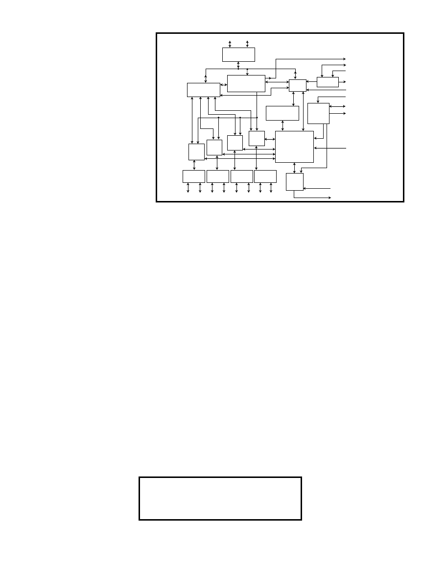
www.circuitcellar.com
CIRCUIT CELLAR
®
Issue 170 September 2004
55
the ’2046 has descriptor tables used to
describe itself as a general-purpose
USB hub. You don’t have to worry
about programming this data correctly
or providing a USB driver for Windows.
However, by pulling the *EXTMEM
input low, you can supply a descriptor
table in an external EEPROM for the
’2046 to use in place of its default.
With the power controller, over-cur-
rent/temperature has a two-level error
function, which first reports an individ-
ual port error and then a total error. The
’2046 can choose to use the bi-level
error by first disabling only the mal-
functioning port (GANGED input low)
or treat all errors as universal by shut-
ting down all ports on any error
(GANGED input high). Along with the
BPMODE from the power controller,
this sets the device into one of four sup-
ported USB power management modes,
Bus-Powered, with either Individual or
Ganged port power management, or
Self-Powered, with either Individual
and Ganged port power management.
When the *EXTMEM pin is tied
high (disabled), the GANGED input is
assumed to be hard-wired. However,
when *EXTMEM is tied low, the
device expects an external EEPROM
to be connected. With an external
EEPROM connected, the GANGED
input is redefined as EEDATA. The
device uses the EEDATA I/O along
with the EECLK output to communi-
cate with the external EEPROM.
For this application, the external
EEPROM must be organized into 64 ×
16 bit words (e.g., 93C46). The device
reads only the first three words. The
first word contains the logic level for
the GANGED. (Remember that the
GANGED input was redefined, but its
value is still necessary.) The second and
third words contain the 16-bit vender
ID (VID) and product ID (PID). This
device installs as a generic USB hub.
On my PC (running XP), I searched
for the USB.INF file, which contains a
list of manufacturers and their VIDs and
PIDs that are recognized as being associ-
ated with the generic driver.
Figure 3 is the section pertain-
ing to Texas Instruments.
If the TUSB2046 had a VID
and PID that matched an
entry in the USB.INF file,
then the device would be
installed as a general-purpose
USB hub. However, in this
It operates on 4.5 to 5.5 V and has an
internal 3.3-V regulator for powering both
itself and other external circuitry. The
’2071 can automatically switch between
Bus- and Self-Powered modes if its local
supply is lost. This would normally cause
the enumeration process to begin again
by logging in as a bus-powered hub.
Downstream power is individually
enabled via inputs (*EN1–4) controlling
internal FETs. One output (OUT1–4)
is for each downstream connector.
Current through each downstream cir-
cuit is monitored for over-current and
over-temperature errors. An over-cur-
rent through a FET forces the supply
into a constant current mode. This
condition, which puts the full voltage
across the FET, produces an increased
dissipation that raises the temperature.
If the die temperature rises to 140°C,
the FET turns off and the error output
(*OC1–4) goes low. If the temperature
reaches 150°C, the device shuts down.
If the BP_DIS input pin is tied low,
the ’2071 can automatically transition
between Bus- and Self-Powered modes.
This is handled by monitoring for a
change at the external power self-power
(SP) input. After a change occurs, the
’2071 goes through a transition sequence
that involves shutting down the device’s
power and powering up again. A low
*BPMODE output indicates the device
is in Bus-Powered mode. The power good
(PG) output also transitions low and
returns high after the mode has changed.
The DP0_RST output also handles signal-
ing the reset to the upstream connection.
CONTROLLING DATA
Texas Instruments split the USB hub
operations into power and data func-
tions. The TUSB2046 four-port hub data
controller is a digital state machine.
A microcontroller and firmware aren’t
required (see Figure 2). It incorporates
version 1.1-compliant USB transceivers
for all upstream and downstream ports.
The ’2046 uses a 48-MHz external
oscillator or generates a 48-MHz
clock from an external 6-MHz
crystal using a PLL. The PLL con-
figuration is necessary if the low-
power Suspend and Resume modes
are going to be implemented.
All USB devices send descrip-
tor data during enumeration, so
Figure 2—
Upstream and downstream communication is handled by the TUSB2046. The data controller enumer-
ates with a host. Along with the power controller, it makes up the majority of the circuitry necessary to expand a sin-
gle USB port into four simultaneous USB connections.
USB
Transceiver
DP0
DM0
1
2
Hub repeater
Suspend/resume
logic and
frame timer
SIE
OSC/PLL
SIE Interface
logic
Serial
EEPROM
interface
Port 4
logic
Port 3
logic
Port 2
logic
Port 1
logic
USB
Tranceiver
USB
Tranceiver
USB
Tranceiver
USB
Tranceiver
24
23
20
19
16
15
12
11
DP4 DM4 DP3 DM3 DP2 DM2 DP1 DM1
Hub/device
command
decoder
Hub
power
logic
10, 14, 18, 22 *OVRCUR1– *OVRCUR4
9, 13, 17, 21 *PWRON1– *PWRON4
32
SUSPND
TSTPLL/48MCLK
27
30
XTAL1
XTAL2
29
*RESET
4
*EXTMEM
26
EEDATA/GANGED
6
EECLK
5
8
BUSPWR
[TI.Section]
%USB\VID_0451&PID_1446.DeviceDesc%=StandardHub.Dev,USB\VID_0451&
PID_1446
and
TI.Mfg="TI"
USB\VID_0451&PID_1446.DeviceDesc="General Purpose USB Hub"
Figure 3—
This entry in the file would have designated this a Texas
Instruments device had the VID and PID matched the file entry. It would
have been listed as a general-purpose USB hub in the device manager.
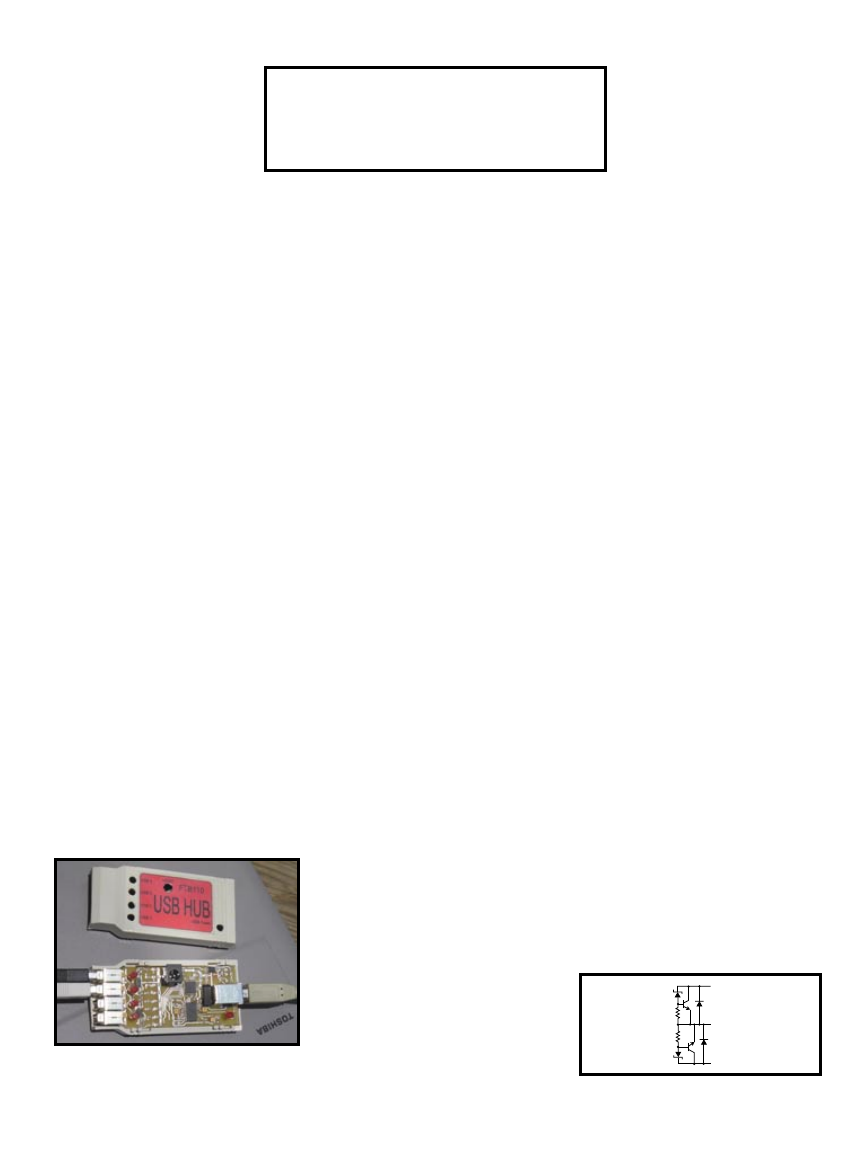
56
Issue 170 September 2004
CIRCUIT CELLAR
®
www.circuitcellar.com
case, the VID and PID are
both “0000,” which doesn’t
match any entry in the
USB.INF file. Therefore, the
device manager selects a best
fit in this case using CLASS
(and SUBCLASS). The device
is installed as a generic USB
hub (see Figure 4).
You can get your own VID
from the USB Implementers Forum
for $1,500 (nonmembers) and register
to use the USB logo on products that
have passed USB-IF compliance test-
ing for the same $1,500. (Registration
for use of the logo is required every
two years.)
SPEAK FOR YOURSELF
The USB hub is special because it must
not only enumerate itself as a USB device,
but also repeat USB packets from the
upstream host/hub to all downstream
devices and from a downstream respond-
ing device to the upstream host/hub. This
includes translating the packet between
upstream and downstream speeds when
necessary. Because this hub is USB ver-
sion 1.1-compliant, a high-speed transac-
tion translator isn’t necessary and
up/downstream connections are limited
to full speed (approximately 1.216 MB of
data per second, bulk transfer).
All USB devices must be able to
enter a suspended state in which they
are limited to 500-µA current draw
from the bus. This state reduces
unnecessary current draw while
devices are not communicating. This
state can be global or selective (i.e.,
the host can suspend individual
devices as well as the whole shebang).
Devices automatically go into a sus-
from ESD transients while
maintaining a low (1 µA) leak-
age current (see Figure 5).
These parts have low input
capacitance (35 pF), which
makes them suitable for USB
1.x applications. Using these
devices properly will improve
the protection capabilities
beyond 15- (HBM) and 2-kV
(MM) levels. As you can see in Photo 1,
the TSOP8 package doesn’t require a
lot of real estate. It also costs less than
$1 (in onesies) to protect two ports.
LAY OF THE LAND
Most of the circuit design time was
spent creating the Texas Instruments
parts in the layout library, not only for
the schematic in Figure 6, but also for
the PCB layout. Texas Instruments has a
reference design that helps answer ques-
tions about how the parts work together.
The TPS2071 comes in a 32-pin
thermally enhanced thin shrink small-
outline package (HTSSOP). The die is
mounted on a power pad, which is
exposed on the bottom surface of the
part. You can enhance the dissipation
of heat by approximately four times by
providing proper PCB design using the
PCB copper as a heatsink. Heat is devel-
oped on the chip across the internal
voltage regulator and the internal FETs.
The TUSB2046 is packaged in a 32-pin
low-profile quad flat pack (LQFP). The
’2071’s regulator supplies its 30-mA oper-
ational requirement, which is at 3.3 V.
I chose to use the eight-pin TSOP
package for the transient protectors.
Three SN65240s protect the power
supply, upstream port, and four down-
stream ports. Because 5-V regulated
supplies are so prevalent, I was able to
eliminate the external FET used by
the ’2071 power controller to preregu-
late a 6- to 9-V power supply input.
Space was at a premium. I wanted
to fit the design in a Pac Tec (CNL-
pended state after bus activity has
ceased for 3 ms. Any bus activity will
trigger a resume state. If a device on
the USB bus has remote wake-up capa-
bility and the host has enabled it, that
device can initiate bus activity (trig-
gering a resume state).
TRANSIENT PROTECTION
The USB hot-pluggable system allows
you to connect or disconnect a peripher-
al when a PC is on without having to
reboot. Bringing two devices together
(with different initial charges) can be
potentially hazardous to either the PC or
the peripheral. Connecting grounds
first is always a good idea, but the ref-
erence puts strain on the other connec-
tions. Protecting these connections from
over-voltage spikes may save the device
(or system) from transient damage.
Another potential for damage comes
from a build up of static charge on your
body (possible from shuffling across the
room) that may be injected into a device
while handling the connection. And
although nothing can protect equipment
from a lightning strike (just ask Steve),
the level of protection is a matter of
choice and the depth of your pockets.
JEDEC Engineering Standards and
Publications documents methods of test-
ing for ESD transients. The human body
model (HBM) is fashioned after the resis-
tive equivalent of the body, while the
machine model (MM) uses a conductive
representation. As a result, slightly dif-
ferent circuits are used to produce ESD
transients in a test environment. The
MM uses a 200-pF capacitor to transfer
a charge while the HBM uses 100 pf in
series with a 1.5-k
Ω
resistor. You’ll often
see discharge ratings like 2 or 15 kV
based on the HBM and MM models.
Texas Instruments has transient
suppressors designed specifically for USB
protection. The SN65220 (single) and
SN65240 (double) SMT parts protect
[GenericHub.Section]
%USB\CLASS_09&SUBCLASS_01.DeviceDesc%=StandardHub.Dev,USB\CLA
SS_09&SUBCLASS_01
%USB\CLASS_09.DeviceDesc%=StandardHub.Dev,USB\CLASS_09
and
GenericHub.Mfg="(Generic USB Hub)"
USB\CLASS_09&SUBCLASS_01.DeviceDesc="Generic USB Hub"
USB\CLASS_09.DeviceDesc="Generic USB Hub"
Figure 4—
A matching entry in the file wasn’t found for a VID of 0000 and PIV
of 0000, so a best fit was used based on CLASS equal to nine and SUBCLASS
equal to one. This is listed in the device manager as a “generic USB hub.”
A or C
GND
B or D
Figure 5—
Here you see the equivalent circuitry used in
the SN65240 USB transient protection device.
Photo 1—
I removed the cover on my USB hub to show the
internals. Now my laptop can have multiple USB devices at
the same time. If necessary, a 5-V wall wart can plug in
through the top of the enclosure to supply additio
nal current.

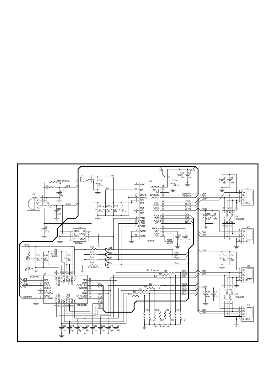
www.circuitcellar.com
CIRCUIT CELLAR
®
Issue 170 September 2004
59
0407) DE-9-to-modular phone jack
molded plastic enclosure. Four vertical
USB downstream connectors fit in the
DE-9 opening, and the upstream con-
nector was a good match for the mod-
ular phone jack opening (see Photo 1).
The SMT pitch for the SN65240 and
TPS2071 is 0.65 mm (approximately four
pins per 0.10
″)
. It’s 0.8 mm (approxi-
mately three pins per 0.10
″
) for the
TUSB2046. These are fairly easy to sol-
der on the PCB using a standard iron
with a fine-point tip. I like to use solder
paste, which is available from most parts
distributors, but it’s a bit pricey. (Keep
unused paste in the refrigerator.) You can
also use thin core solder if you squeeze it
flat with smooth jaw pliers and cut it
into thin strips with cutters. Solderwick
is also an important tool for removing
solder that has bridged two adjacent pins.
PACKAGING
The standard Pac Tec enclosure
needs little modification. The small
tabs are trimmed away from the DE-9
end, fully exposing the middle two USB
connectors. Holes for the five LEDs and
power jack are placed in the top. Use a
drill press or hole punch. You might
want to leave off the five LEDs until
you can adjust them for the right height
to protrude through the plastic top.
Any drawing program can be used to
design a label. I print on adhesive label
material and cover the graphics with a
piece of clear packing tape to protect the
surface. If I were to work on another
PCB layout, I would move all the LEDs
about 0.3
″
toward the center. This would
allow them to be underneath the label and
sealed. It isn’t a big deal because the power
jack and USB connectors aren’t sealed.
This small project is a great addition
to my laptop after I plug in a mouse. I
now have room for additional periph-
erals like a printer, digital camera, or
joystick for flying the space shuttle
simulator. For most peripherals, Bus-
Powered mode is sufficient, but when
I need it, the 5-V power supply gives
me 0.5 A for each downstream port.
COMPLIANCE PROGRAM
Designing a new interface protocol
(USB) is only half the story. To ensure
that all of the marketed products actual-
ly work together, the USB Implementers
Forum created a series of compliance
tests. Devices that successfully pass the
compliance program testing are added to
the integrator’s list of compliant devices.
The compliance program requires a
manufacturer to submit a USB compli-
ance checklist, which includes questions
that will be verified by compliance test-
ing. Inrush current testing is a measure-
ment of the initial hot-plug current of
your previously discharged hub under test
(HUT). Upstream signal quality testing
is a view of the signal integrity between
your HUT and the upstream hub.
Figure 6—
Only a handful of discretes besides the five TI parts are necessary to create a four-port USB hub. The SMT parts allow all the circuitry to fit within a small stock plastic enclosure.
60
Issue 170 September 2004
CIRCUIT CELLAR
®
www.circuitcellar.com
When performing host or hub power
provider (droop/drop) testing, the droop
test determines the affect of hot plug-
ging on the V
BUS
of adjacent downstream
ports. The drop test is the amount of
loss on V
BUS
when the port is loaded.
Hub downstream signal quality testing
is a view of the signal integrity between
your HUT and a downstream device.
Device framework testing involves
using the USBCommandVerifier.exe
(USBCV) program to test data communica-
tion. USBCV tests all the commands for
a proper result. The average current
must be measured to make
sure that the device will
enumerate with less than
or equal to 100 mA.
Back-voltage testing
ensures that the device
won’t source current
upstream if V
BUS
is not avail-
able. Finally, device interop-
erability testing is done on
the HUT using various
configurations of EHCI,
UHCI, and OHCI USB con-
trollers at the maximum
tier allowed by the system. The maxi-
mum cabled lengths with a variety of
installed devices are used.
USBCV
Although the equipment to run the
compliance program’s test setups can
be pricey, you can run the free USB
command verifier (www.usb.org) on
your own PC. That’s if you’re running
Windows XP with a USB 2.0 host con-
troller/root hub and one USB2.0 hub.
I ran through the hub and Chapter 9
tests (see Photo 2). The results prove that
the VID and ID are both 0000. (I had
expected to see a VID of 0451 and possi-
bly a PID of 2046, which would have
meant that the manufacturer is Texas
Instruments and the device a 2046.)
With all command tests passing the
USBCV, I guess I feel comfortable
enough to get down to business. So,
you’ll have to excuse me, I have a
scheduled launch at the International
Space Station this afternoon.
Something about some needed supplies
for the Expedition 9 crew.
I
Photo 2—
The USB command verifier application swaps out the standard
Microsoft USB 2.0 driver and installs a test stack driver, thereby taking
complete control for testing purposes. The present version has five test
areas where commands can be tested automatically or selectively. The
standard drivers are replaced when you exit the application.
Jeff Bachiochi (pronounced BAH-key-
AH-key) has been writing for
Circuit
Cellar since 1988. His background
includes product design and manu-
facturing. He may be reached at
jeff.bachiochi@circuitcellar.com.
SOURCES
CNL-0407 Plastic enclosure
Pac Tec
www.pactecenclosures.com
TPS2071, TUSB2046, and SN65240
Texas Instruments, Inc.
www.ti.com

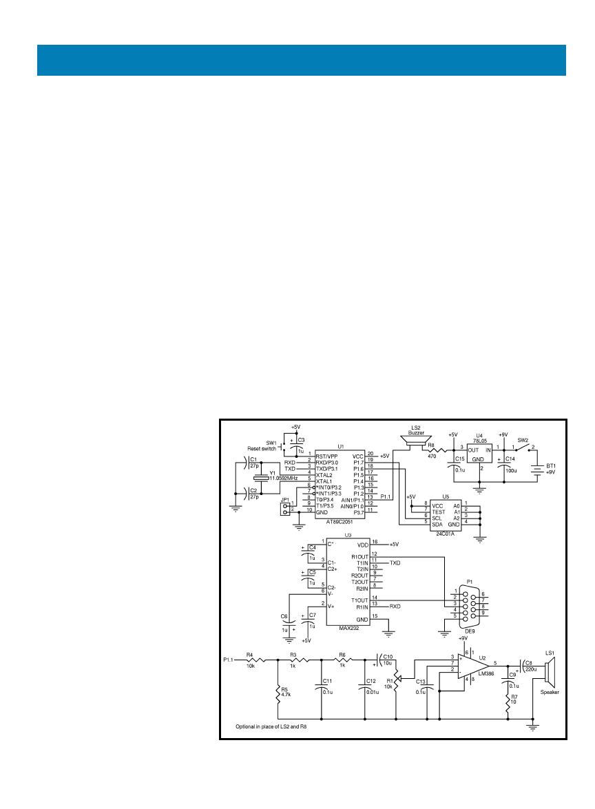
resource to produce a square wave (in
audio range) similar to the IBM PC.
FIRST MUSICAL ATTEMPT
You can use a piezoelectric buzzer
or a loud speaker to produce sound
waves. Piezoelectric buzzers are avail-
able as self-oscillating buzzers with
signal generators and buzzers without
signal generators. For this project, you
need a buzzer without a signal genera-
tor. The microcontroller firmware
generates the tone signal and the
buzzer converts it to sound output. If
your microcontroller I/O port supports
62
Issue 170 September 2004
CIRCUIT CELLAR
®
www.circuitcellar.com
W
e were asked to develop a digital
clock. The requirement was to display
the time in various formats and incor-
porate a melodious alarm. Conventional
hand clocks do not recognize whether
it’s morning or evening. Our clock dis-
plays both in a 12-h format. Another
requirement was that the clock must
be able to keep track of the date and
the day of the week.
There are special integrated circuits
available in small eight-pin packages
that produce melodies. But these
sound chips lack programmability! We
decided to use a microcontroller
instead of a dedicated clock IC. This
also cut the cost of the project.
In this article, we’ll explain how to
generate sounds using an MCS-51
microcontroller. Even though we used
MCS-51 architecture, the concept is
easily adopted to the microcontroller
of your choice, provided you can gen-
erate a square wave. We’ll cover the
topic of sound generation, from musi-
cal notes to the monophonic ring
tones used by mobile phones.
Thousands of ring tones are available
for free on the Internet. You can
download these ring tones to give your
digital clock or doorbell a unique
sound!
Our first experience with audible
alarm generation involved using the
popular timer IC555 configured as an
astable multivibrator. In its early days,
the IBM PC produced sounds using
one of the channels of Intel’s 8253 pro-
grammable timer/counter IC. There
was no sound card, and computer
games used the timer to generate
robot and machine gun sound effects.
Microsoft QuickBASIC for MS-DOS
supported sound generation by adding
Adding tunes and tones to embedded applications just got easier. Praveen and Prajakta
show you how to generate melodies with an MCS-51 microcontroller.
a built-in play note command, which
played musical notes through the PC’s
speakers. Even the popular Turbo C
DOS compiler had a library function,
sound(frequency), to generate rudi-
mentary sounds.
Most of the microcontrollers avail-
able today have one or more timer/
counters. This resource is meant for
handling critical application-timing
requirements. Some chips provide the
timer output on one of the output pins.
Others enable you to generate an inter-
rupt after timer overflow. To generate
sound effects, you can program a timer
FEATURE ARTICLE
by Praveen Deshpande & Prajakta Deshpande
Microcontroller-Driven Sound Effects
Figure 1—
Our design features a microcontroller, audio amplifier, and speaker. This circuit can be used as a musi-
cal doorbell.

64
Issue 170 September 2004
CIRCUIT CELLAR
®
www.circuitcellar.com
high-current driving (e.g., 20 mA for the
AT89C2051), you can drive the buzzer
directly using a port pin. Alternatively,
you can use an audio amplifier to drive
an 8-
Ω
speaker (see Figure 1).
We had no specific reasons for
choosing the MCS-51. Basically, we’re
familiar with it and have some experi-
ence with the MCS-51 family. The
8051 has two on-chip timers, Timer0
and Timer1. The on-chip UART
requires Timer1 for data rate clock
generation in Asynchronous
Communication mode.
Using an RS-232 serial interface to
download melody files occupies
Timer1. The remaining timer (Timer0)
is free and used to generate the
melody. The 16-bit timer register is
incremented at the oscillator frequen-
cy divided by 12. The Timer0 output
pin isn’t directly accessible for driving
a buzzer. Instead, an internal flag—
TF0 (timer control TCON register)—is
set to 1 every time the 16-bit timer
register (TH0:TL0) overflows from
FFFFH to 0000H. The TF0 flag can
generate a Timer0 interrupt if you
enable it using the interrupt enable
register (IE). It’s cleared automatically
by the on-chip hardware when the
service routine is vectored to. Thus, to
generate a square wave using the
Timer0 interrupt service routine (ISR),
you must toggle a port pin inside the
ISR. The timer0 overflow rate must be
equal to the frequency of the desired
square wave (see Listing 1).
The duration of the generated tone
can be implemented using a software
loop. The
Sound() function has two
arguments, frequency in hertz and
duration in milliseconds. It computes
the 16-bit timer reload value for the
oscillator frequency. If you execute
the code, you should hear beep and
sound effects similar to a computer
game’s. You can experiment by chang-
ing the frequency and duration, and
adding more sound statements to
compose your own melody.
MUSIC THEORY
Listing 1 shows you a way to com-
pose your own melody by adjusting
three parameters: frequency, duration,
and the pause between two successive
tones. The musical instrument plays a
Table 1—
The musical note frequency corresponding to each octave is tabulated for reference. We computed a 16-bit
reload value for generating the note using a MCS-51 Timer0 (operating in mode 1) with a 11.0592-MHz crystal oscillator.
Octave = 5
Octave = 6
Note
Desired
Actual
Counter
Note
Desired
Actual
Counter
frequency
frequency
reload value
frequency
frequency
reload value
A
440Hz
439.85 Hz
0FBF5H
A
880 Hz
880.55 Hz
0FE00H
A#
466 Hz
466.59 Hz
0FC30H
A#
932 Hz
934.13 Hz
0FE1EH
B
494 Hz
494.66 Hz
0FC68H
B
988 Hz
986.14 Hz
0FE39H
C
523 Hz
522.73 Hz
0FC9BH
C
1047 Hz
1049.04 Hz
0FE54H
C#
554 Hz
554.18 Hz
0FCCDH
C#
1109 Hz
1109.71 Hz
0FE6DH
D
587 Hz
586.66 Hz
0FCFBH
D
1175 Hz
1177.82 Hz
0FE84H
D#
622 Hz
621.49 Hz
0FD27H
D#
1244 Hz
1241.32 Hz
0FE99H
E
659 Hz
658.84 Hz
0FD50H
E
1319 Hz
1319.5 Hz
0FEAFH
F
698 Hz
698.83 Hz
0FD78H
F
1397 Hz
1399.78 Hz
0FEC2H
F#
740 Hz
739.21 Hz
0FD9DH
F#
1480 Hz
1480.8 Hz
0FED5H
G
784 Hz
784.55 Hz
0FDC0H
G
1568 Hz
1571.77 Hz
0FEE6H
G#
830 Hz
829.78 Hz
0FDE0H
G#
1660 Hz
1662.56 Hz
0FEF7H
Octave = 7
Octave = 8
A
1760 Hz
1764.48 Hz
0FF06H
A
3520 Hz
3515.48 Hz
0FF88H
A#
1865 Hz
1864.49 Hz
0FF14H
A#
3729 Hz
3744.13 Hz
0FF90H
B
1976 Hz
1976.52 Hz
0FF22H
B
3951 Hz
3936.14 Hz
0FF96H
C
2093 Hz
2100.30 Hz
0FF2FH
C
4186 Hz
4148.90 Hz
0FF9DH
C#
2218 Hz
2224.78 Hz
0FF3CH
C#
4435 Hz
4471.15 Hz
0FFA4H
D
2349 Hz
2361.68 Hz
0FF48H
D
4699 Hz
4651.80 Hz
0FFA9H
D#
2489 Hz
2489.34 Hz
0FF53H
D#
4978 Hz
4951.92 Hz
0FFAEH
E
2637 Hz
2631.59 Hz
0FF5DH
E
5274 Hz
5293.43 Hz
0FFB4H
F
2794 Hz
2791.08 Hz
0FF67H
F
5588 Hz
5548.54 Hz
0FFB9H
F#
2960 Hz
2971.15 Hz
0FF70H
F#
5920 Hz
5980.89 Hz
0FFBEH
G
3136 Hz
3132.85 Hz
0FF79H
G
6272 Hz
6308.61 Hz
0FFC2H
G#
3320 Hz
3313.15 Hz
0FF80H
G#
6640 Hz
6674.32 Hz
0FFC6H
www.circuitcellar.com
CIRCUIT CELLAR
®
Issue 170 September 2004
65
specific tone when you
strike a key.
Music notation
is a system
of writing music. The term
sheet music is used for writ-
ten music to distinguish it
from audio recordings. A
musical note refers to a unit of
fixed pitch that has been given
a name, as well as the graphic
representation of that pitch
in a notation system. These
notes have letter names: A, B,
C, D, E, F, and G. Each letter
is assigned to a specific pitch
regardless of the octave in
which the pitch resides.
Notes are used together as
scales (tone rows). However,
because 12 notes are needed,
the seven letter names also
can be given a modifier. The
two main modifiers are
sharps and flats, which
respectively raise and lower
the pitch of a note by a
semitone. These are used to
create the additional five
notes necessary to complete
the chromatic scale. The
sharp symbol is #, and the
flat symbol is I.
Note durations are not
recorded on sheet music in
terms of milliseconds;
instead, they are described
as whole, half, quarter,
eight, sixteenth, and thirty-
second notes. As the name
suggests, a half note lasts
half as long as a whole note.
A quarter note lasts one-
fourth the time of a whole
note. The duration of a
whole note depends on the
piece of music being played.
One piece might be played
at a tempo (or speed) that
causes a whole note to last
for 4 s. Another piece might
have a 2-s whole note. A
rest is the time between
notes when no tones are
played. Rest durations are
also measured in whole,
half, quarter, eighth, six-
<ringing-tones-text-transfer-language> :=
<name> <sep> [<defaults>] <sep> <note-command>+
<name> := <char>+ ; maximum name length 10 characters
<sep> := “:”
<defaults> := <def-note-duration> | <def-note-scale> | <def-beats>
<def-note-duration> := “d=” <duration>
<def-note-scale> := “o=” <scale>
<def-beats> := “b=” <beats-per-minute>
<beat-per-minute> := 25,28,...,900 ; decimal value
; If not specified, defaults are
; duration=4, scale(octave)=6, beat-per-minute=63
<note-command> :=[<duration>] <note> [<scale>] [<special-duration>] <delimiter>
<duration> :=
“1” | ; full 1/1 note
“2” | ; 1/2 note
“4” | ; 1/4 note
“8” | ; 1/8 note
“16” | ; 1/16 note
“32” | ; 1/32 note
<note> := “C” |“C#” | “D” | “D#” | “E” | “E#” | “F” | “G” | “G#” | “A” | “A#” | “P” ; “P” = pause
<scale> :=
“5” | ; Note A is 440Hz
“6” | ; Note A is 880Hz
“7” | ; Note A is 1.76 kHz
“8” ; Note A is 3.52 kHz
<special-duration> ;=
“. ” ; Dotted note
<delimiter> := “ , ”
Sample RTTTL-format ringtone (Imperial theme from Star Wars):
Imperial:d=4,o=5,b=100:e,e,e,8c,16p,16g,e,8c,16p,16g,e,p,b,b,b,8c6,16p,16g,d#,8c,16p,
16g,e,8p
Figure 2—
Take a look at the specifications and syntax rules for RTTTL format. The
Nokia mobile phone uses this standard to store monophonic ring tones, plenty of
which are available for free on the Internet.

66
Issue 170 September 2004
CIRCUIT CELLAR
®
www.circuitcellar.com
teenth, and thirty-seconds.
A musical octave is the interval
between one musical note and another
whose pitch is twice its frequency. For
example, if one note is pitched at
400 Hz, the note an octave above it is at
800 Hz and the note an octave below is
at 200 Hz. The ratio of frequencies of
two notes an octave apart is therefore
2:1. See the frequencies assigned for var-
ious notes and octaves in Table 1.
You can mimic a piano by generat-
ing the tones corresponding to its key.
To play a song, you need the sequence
of the piano keys (notes), the octave
used, and the duration of each note.
CELLULAR RING TONES
The ringing tones text transfer lan-
guage (RTTTL) format is one of the
most popular standard specifications
(see Figure 2). Nokia mobile phones use
it for playing back monophonic ring
tones. The great thing about RTTTL
files is that they are shared on the ’Net.
Many sites have RTTTL files available
for free. There are also free software pro-
grams that you can use to compose and
emulate these files and download them
to your cell phone. The tunes can be
transported using .RTX ring tone speci-
fications, which are ASCII text files that
include information about its name,
default attributes, and a comma-delim-
ited string of notes that are optionally
supplied with octave and duration.
The code fragment for decoding the
ring tone is shown in Listing 2. The ring
tone file contains a header to specify the
title of the tone and default parameters
such as the note duration, octave, tempo
of the tune in bits per minute (bmp), and
so on. If a parameter is not explicitly
specified, you should use the default
value (see Figure 2). The body of the note
command is made up of comma-delimit-
ed notes prefixed by optional duration
and post-fixed by octave. A dotted note
is specified after the octave, which indi-
cates the duration of the note, is extend-
ed by 50% of the specified duration. The
RTTTL file is stored in an array and
scanned sequentially to gather informa-
tion about the notes. Header information
such as the title is omitted because it
does not contribute to the melody.
The variables are initialized with default
values of duration and octave.
The full note duration is computed
from the tempo information. A
ptr
variable is used as an index to
Tune[]
to read one character from the array.
The code parses the array to check if
note duration is specified. The
dura-
tion variable is updated only if a
valid value (1, 2, 4, 8, 16, or 32) is
encountered. The code scans the array
for a musical note. A
FreqOctX[]
array holds 16-bit timer reload values
corresponding to note frequencies (see
Table 1). There are four arrays (
X in
FreqOctX[] equals 5, 6, 7, or 8) to hold
the reload values for 12 notes corre-
sponding to four octaves: 5, 6, 7, and
8. Depending on the presence of a
#
attribute, either a
FetchSharpNote()
or
FetchNote() function returns an
index to
FreqOctX[] array.
As per the RTTTL specifications,
the dotted notation to extend the note
duration is specified after the octave.
If a dot is found, the information is
temporarily stored in the
duration
variable by setting its most significant

www.circuitcellar.com
CIRCUIT CELLAR
®
Issue 170 September 2004
67
bit to 1. The
FetchOctave() function
scans for a numeric octave value (5
through 8), and the
ptr variable is
incremented by one. Therefore, the
code has fetched all the necessary
information for playing the note.
The
PlayNote() function is called
with three arguments: note duration, its
octave, and its index in
FreqOctX[].
GetNoteTblPtr() returns the pointer
to the current note octave table
(
FreqOctX). The note duration is con-
verted to a value in milliseconds by
dividing the entire note duration by a
specified duration. The 16-bit Timer0
reload value is loaded into the TH0:TL0
timer registers for frequency generation.
The Timer0 run flag (TR0) is set to 1 to
start the timer. The Timer0 overflow
sets a TF0 flag that invokes a Timer0
interrupt. The interrupt service routine
toggles the P1.1 port pin generating the
tone. This process continues for the
duration of the note, and the code stops
the Timer0 by clearing the TR0 bit.
The code continues parsing the
Tune[]
array for next note until the end of all
the notes in the array. The Timer0 ISR
code is exactly identical to the one
shown in Listing 1.
You can easily store many ring tone
ASCII files in the ROM before you com-
pile your code in a separate array. You
can then declare another array to hold
the pointer to these ring tone arrays.
This way, you can programmatically
play a specific ring tone as per your
application requirements. Alternatively,
you can store the ring tone files in
NVRAM or EEPROM. This enables you
to download new ring tone files at any
time using an RS-232 serial interface.
We used a Keil C compiler for this
project. You can use any C compiler and
any microcontroller with a 16-bit timer
and one spare output pin for driving the
speaker. With a Keil C compiler, the
compiled code occupies about 1 KB of
ROM along with a few ring tone files.
We used an AT89C2051 (2-KB code
memory). If the ring tone files are larger,
and if you want to include additional
ring tones for your application, then you
might run out of memory. You’ll need
more memory to write application code
apart from melody maker code. We were
faced with this problem. You can save
memory. How? Compress the ring tone
files before storing.
SQUEEZE THE MELODY
By storing the ring tone files in the
ROM after downloading them, you’re
consuming more memory because
you are storing them in ASCII format.
Each note in ASCII format consumes
at least 2 or 3 bytes (e.g., A or C#)
even though the default duration and
octave setting are applied. If each piece
of note information is specified (e.g.,
32F#7), a single note consumes approxi-
mately 7 bytes of space. If you store this
information in binary format, you can
do a lot of bit stuffing to compress all
the information into 1 or 2 bytes. This
process requires preprocessing or com-
Listing 1—
You can produce sound effects using Timer0. A combination of multiple
sound() statements
generates a variety of sound effects.
#include <reg51.h>
// 8051-specific definitions
#define OSC_FREQ 11059200L
// oscillator frequency in hertz
struct _intbytes {
// structure to share bytes
unsigned char hb;
// with an integer and vice versa
unsigned char lb;
};
typedef union {
// Data structure to extract
unsigned int i;
// upper and lower data bytes
struct _intbytes b;
// from a unsigned integer and
}uIntBytes;
// vice versa
sbit SPEAKER = P1^1;
// Speaker hooked to P1.1
uIntBytes PreloadT1;
// 16-bit Timer0 reload value
void Timer0ISR (void) interrupt 1 // Timer0 ISR (Keil C51 way)
{
TH0 = PreloadT1.b.hb;
// Reload COUNTHIGH;
TL0 = PreloadT1.b.lb;
// Reload COUNTLOW;
SPEAKER = ~SPEAKER;
// Toggle speaker port line (P1.1)
}
void Delay1ms (void)
// Software delay loop for 1 ms
{
register char ch;
// You may need to adjust this
ch = 150;
// as per your compiler!!!!
while(ch—);
}
void Sound (unsigned int freq, unsigned int duration)
{
PreloadT1.i = 65535 - (OSC_FREQ/(12*freq)) + 8;
TR0=1;
// Run Timer0
while(duration—) Delay1ms(); // for requested duration in ms
TR0=0;
// stop Timer0
}
void Pause (unsigned int duration)
{
while(duration—) Delay1ms(); // Silence for requested duration
}
main()
{
int d, freq;
TMOD = 0x11;
// init timer #0 mode 1
ET0 = 1;
// Enable Timer0 interrupt
EA=1;
// Enable 8051 interrupt system
while(1) {
Pause(100);
// Silence for 0.5 s
Sound(1500,1000);
// 1-s beep (1.5 kHz)
Pause(500);
// Silence for 0.5 s
Pause(100);
// cCmputer game sound effect
Sound(2800,100);
// 2.8-kHz tone for 0.1 s
Sound(2400,200);
// 2.4-kHz tone for 0.2 s
Sound(4200,140);
// 4.2-kHz tone for 0.14 s
Pause(500);
// Silence for 0.5 s
Pause(100);
// Alien sound effect
for (d=15; d >= 1; d—) { // continuously reduce duration
for (freq=2000; freq <= 2500; freq += 20)
Sound(freq,d);
// increasing the frequency
}
}
}

68
Issue 170 September 2004
CIRCUIT CELLAR
®
www.circuitcellar.com
piling the ring tone file before download-
ing to the melody hardware. We devel-
oped such a compiler in Visual Basic.
Compiling the ring tone file has
another advantage. You can simplify
the melody player code by eliminating
the ring tone file syntax checker.
Parsing reduces its size even more.
The ring tone compiler is straightfor-
ward (see Photo 1). Copy the downloaded
ring tone file in RTTTL format to the
ring tone input text box. Then, click the
Compile button. The compiler scans the
ring tone file header to record the default
parameters in the internal variables. It
reads each note and converts them into
compiled binary format by stuffing note
information in a byte (default note
length and octave) or two (see Figure 3).
At first glance, you might get the
impression that few control bits (TOI1,
TOI2, LON, etc.) are scattered in a 16-
bit word. But this is done to accommo-
date a note with default parameters in a
single byte. You can even listen to the
melody on the PC.
The Preview button invokes a DOS
application to play the compiled ring
tone file. The compiler downloads the
compiled ring tone file to your melody
hardware using the RS-232 serial inter-
face. You can download the source
code for the ring tone file compiler
from the Circuit Cellar ftp site.
BACKGROUND MUSIC
If you use one more timer (e.g., Timer1)
to generate the note duration in Interrupt
mode, you can create background music.
The Timer1 ISR is a 1-ms tick interrupt
counting and waiting for the note to fin-
ish. It then reloads Timer0 with the
appropriate 16-bit value for the next note
in the queue and continues to play all
the notes in this manner. Because the
melody-related code is executed from the
Timer1 ISR (in the background), the CPU
is free to perform the main task in the
foreground. This enables you to play a
tune in the background while you move
(e.g., a stepper motor in the foreground).
A few members of the MCS-51 fam-
ily of microcontrollers (e.g., the
Philips P89C51Rxx) have a powerful
on-chip peripheral resource called a
programmable counter array (PCA).
The PCA provides more timing capa-
bilities with less CPU intervention
Listing 2—
This code fragment is for decoding and playing the RTTTL ring tone file. The ring tone is stored in
an array after stripping its header information to save space.
code unsigned char Tune[]=”8g.,16g,a,g,c6,2b,8g.,16g,a,g,d6,2c6,8g.,”;
code unsigned int FreqOct7[] = {// Store notes in octave7
0xFF06, 0xFF14, 0xFF22, 0xFF2F, 0xFF3C, 0xFF48, // A A# B C C# D
0xFF53, 0xFF5D, 0xFF67, 0xFF70, 0xFF79, 0xFF80}; // D# E F F# G G#
//Code fragment to parse RTTTL format ring tone file from Tune[] array
do {
Duration = DefDuration;
Octave = FreqOct6;
// default octave is 6
while( Tune[ptr] == ‘,’ || Tune[ptr] == ‘ ‘) ptr++;
NoteIndex = 50; // pause
if((Tune[ptr] == ‘3’) && (Tune[ptr+1] == ‘2’)){ // 1/32
Duration = 32;
ptr += 2;
}
else if ((Tune[ptr] == ‘1’) && (Tune[ptr+1] == ‘6’)){ // 1/16
Duration = 16;
ptr += 2;
}
else if (Tune[ptr] == ‘8’) { // 1/8
Duration = 8;
ptr++;
}
else if (Tune[ptr] == ‘4’) {// 1/4
Duration = 4;
ptr++;
}
else if (Tune[ptr] == ‘2’) {// 1/2
Duration = 2;
ptr++;
}
else if (Tune[ptr] == ‘1’) {// 1
Duration = 1;
ptr++;
}
if (Tune[ptr+1] == ‘#’) {
NoteIndex = FetchSharpNote(Tune[ptr]);
ptr += 2;
}
else {
NoteIndex = FetchNote(Tune[ptr]);
ptr++;
}
if (Tune[ptr] == ‘.’) {
// Duration = 1.5x
Duration |= 0x80;
ptr++;
}
// See if octave is specified
NoteOctave = FetchOctave(Tune[ptr]); // inc ‘ptr’ if found
if (Tune[ptr] == ‘.’) {
Duration |= 0x80;
ptr++;
}
PlayNote(NoteIndex, NoteOctave, Duration); //Play note to speaker
} while(Tune[ptr] == ‘,’ || Tune[ptr] == ‘ ‘);
// Note is index of FreqOct array 0-A, 1-A#, 2-B, etc
void PlayNote(char note, char octave, char duration)
{
unsigned int note_duration;
uIntBytes temp;
Octave = GetNoteTblPtr(octave); // Get FreqTbl array ptr
PreloadT1.i = Octave[note];
NoteDuration = WholeNoteDuration/(duration & 0x7F);
if(duration& 0x80)NoteDuration +=(NoteDuration>>1);
//Durationx1.5
// Start playing the note for the NoteDuration
SPEAKER = 1; // Switch off sound
note_duration = NoteDuration;
TH0 = PreloadT1.b.hb;
TL0 = PreloadT1.b.lb;
if (note != 50) TR0 = 1;
while(note_duration—)Delay1ms();
(Continued)

www.circuitcellar.com
CIRCUIT CELLAR
®
Issue 170 September 2004
69
than the standard timer/counters. Its
advantages include reduced software
overhead and improved accuracy.
The PCA consists of a dedicated
timer/counter that serves as the time-
base for an array of five compare/cap-
ture modules (P1.3–P1.7). The PCA
timer and modules are all 16 bits. If an
external event is associated with a
module, that function is shared with
the corresponding port 1 pin. If the
module is not using the port pin, the
pin can still be used for standard I/O.
These modules can be used to imple-
ment a variety of timing applications.
[1]
The PCA module generates a PCA
interrupt (vector location 0033H),
which is common to all the modules.
Listing 2—
Continued.
// Output tone for note_duration
TR0 = 0;
// Stop timer0
SPEAKER = 1;
// Switch off sound
}
The ISR code may test the CCFn event
flag, which is located in counter control
register (CCON); it corresponds to each
module to discover which module trig-
gered the interrupt. Each module also
has a pair of 8-bit compare/capture reg-
isters (CCAPnH, CCAPnL) and a mode
register (CCAPMn) associated with it.
We used two PCA modules for gener-
ating a melody in the background. (You
can download the code to see how we
did this from the Circuit Cellar ftp
site.) Module0 is configured in High-
Speed Output (HSO) mode to generate
the note frequency. Module4 is config-
ured as a software timer for generating
the note duration. The PCA timer is a
free-running 16-bit timer controlled by
the CR bit in the CCON register.
HSO mode toggles a port pin when a
match occurs between the PCA timer
and the preloaded value in the compare
registers. It’s more accurate than tog-
gling pins in software because the tog-
gle occurs before branching to an inter-
rupt (i.e., interrupt latency will not
affect the accuracy of the output).
The software timer generates the
PCA interrupts once per millisecond
and the note duration is adjusted. The
code checks for the remaining time for
the current note and loads the Module0
compare registers with new values cor-
responding to the next note. The avail-
ability of multiple PCA modules enable
you to play up to four notes simultane-
ously. The DTMF standard requires
generating two frequencies simultane-
ously while dialing a telephone number!
SINGING DOORBELL
Let’s take a look at a doorbell system
that plays ring tones. The system has
enough memory to hold numerous ring
tones. When you’re fed up with the
repeated tunes, you can download new
ones to the on-board 128-byte serial
EEPROM using the ring tone compiler
utility (see Photo 1). This single-chip
application is based on the AT89C2051
20-pin microcontroller (see Figure 1).
The microcontroller normally remains
in Power Down mode. The Reset but-
ton wakes it up. Then, it plays a tune,
updates the pointer to the next song, and
returns to Power Down mode. The
microcontroller must be in Power Down
mode to remember the last song played
Listing 3—
This is how you can play the melody in the background. You can use another timer or PCA hard-
ware for timing the musical notes.
// Code fragment for background melody using PCA hardware
#include <reg51f.h>
// P89C51RD2 definitions
#define
OSC_FREQ
11059200L
// Osc frequency in hertz
uIntBytes PreloadM0, PreloadM4; // Struct/union to split integers
unsigned int ValM0, ValDelay1ms, Note_ms_duration;
char TuneIndex;
code unsigned int Tune[] = {2800, 100, 2400, 200, 4200, 140};
void BGMusic(void)
{
PreloadM4.i += ValDelay1ms; // 1-ms duration
CCAP4L = PreloadM4.b.lb;
CCAP4H = PreloadM4.b.hb;
if(Note_ms_duration) {
Note_ms_duration—; // Continue the note freq. generation
}
else {
// Note duration over
if (TuneIndex > 5) TuneIndex = 0; // Load next note freq.
ValM0 = (OSC_FREQ/(12*Tune[TuneIndex++])); // Compute value
Note_ms_duration = Tune[TuneIndex++];
}
}
void PCAMelodyISR(void) interrupt 6 using 0 // PCA interrupt
{
if (CCF0) {
// PCA Module0 event
CCF0 = 0;
// clear PCA overflow flag
PreloadM0.i += ValM0;
// reload count
CCAP0L = PreloadM0.b.lb; // in module registers
CCAP0H = PreloadM0.b.hb;
}
if (CCF4) {
// Module 4 PCA 1-ms interrupt
BGMusic();
// play notes in Tune[]
}
}
main()
{
ValDelay1ms = (OSC_FREQ/12);// 1-ms duration
CMOD = 0x0;
// PCA clock 1/12 osc freq
CL = CH = 0;
CCAPM0 = 0x4D;
// PCA0 in HSO with interrupt
CCAP0L = PreloadM0.b.lb;
CCAP0H = PreloadM0.b.hb;
CCAPM4 = 0x49;
// PCA4 s/w timer mode with INT
PreloadM4.i = ValDelay1ms = (OSC_FREQ/12); // 1-ms duration
CCAP4L = PreloadM4.b.lb;
CCAP4H = PreloadM4.b.hb;
CR = 1;
// Run PCA timer
EA = EC = 1;
// Enable PCA interrupt
while(1) { // This loop executes the foreground activity
// TODO: add code here for your foreground activity
}
}
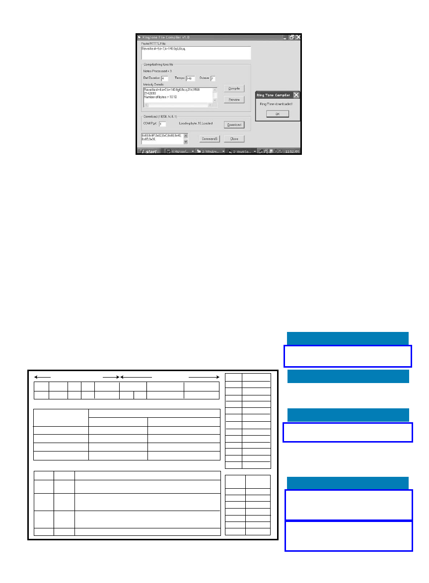
so that it isn’t repeated. Similar
functionality can be implement-
ed with an EEPROM by storing
song information. Then the
power can be switched off to
extend the battery life.
To download the ring tones
in binary format, connect the
doorbell’s RS-232 cable to a
PC. A jumper (JP1) selects the
doorbell’s Download and Play
modes. Insert the shorting
jumper at JP1 and press the
Reset button. The doorbell is
now in Ring Tone Reception
mode. On the PC side, run the
ring tone compiler application,
convert the required ring tone
file to binary format, and click the
Download button. The result is a
“Ring Tone Downloaded!” pop-up
message on the screen. After this,
remove JP1 and push the Reset button.
You’ll hear the downloaded ring tone.
We used a 9-VDC battery. IC U4
(78L05 regulator) generates a 5-V logic
supply for U1 (AT89C2051) and U5 (seri-
al EEPROM 24C01A). U3 (MAX232)
converts the logic level signals to RS-232
for connecting the doorbell to a PC. An
audio amplifier (IC U2) based on LM386
reproduces the song loud enough to hear
it anywhere in your house. Although the
circuit does not have a provision to
programmatically switch off the power
to the microcontroller and audio
amplifier circuit, it should be included
to extend the battery life.
YOUR ASSIGNMENT
As you can see, using a microcon-
troller to produce melodies is a simple
task. We started developing this code
for an assignment, but later the hobby-
ists inside us took over. Our results
encouraged us to develop code for a
full-blown generic melody API for the
MCS-51 microcontroller family.
You’ll find our tools (e.g., the ring
tone file compiler) useful for down-
loading the melodies to the hardware
using an RS-232 serial interface. For
this reason, we posted them on the
Circuit Cellar
ftp site. If you want to
learn more, read up on the musi-
cal instruments digital interface
(MIDI) standard, which allows
you to play numerous musical
notes simultaneously. Moreover,
the polyphonic ring tones
played by many mobile phones
have a file format and capability
similar to MIDI instruments.
You can also play two or more
notes simultaneously using
PCA hardware.
We’ve supplied you with the
information. Your assignment
is to think about how to incorpo-
rate a melody API in your next
embedded application to make it
more interesting and fun. We
wish you a melodious instrumentation.
I
70
Issue 170 September 2004
CIRCUIT CELLAR
®
www.circuitcellar.com
Figure 3—
You can compress musical note information in 1 or 2 bytes and stack melody files end-to-end in an EEPROM.
MSB (8-bit) (D15–D8) LSB (D7–D0)
1-bit 1-bit 1-bit
1-bit 4-bit
2-bit
3-bit
3-bit
LON Dotted
L=4 O=6 Note code TOI1 TOI2 Note length code Octave Number
Description of individual fields in the MSB
Field
Value
0
1
LON (length of note)
Note occupies 1 byte
Note occupies 2 bytes
Dotted
–
Note length = note length × 1.5
L=4
Note length is specified
Note length = 4 (default)
O=6
Note octave is specified
Note octave = 6 (default)
Description of individual fields in LSB
TOI1
TOI2
Type of Information (TOI) descriptor field
1
0
This is a 2-byte header. The note length code holds the default length.
The Octave Number field holds the default octave value.
1
1
This is the second part of the header containing the 13-bit (BMP)
tempo for the song. The upper 7 bits are D14–D8 and the lower
6 bits are D5–D0.
0
1
This is the third part of the header containing the total length (in bytes)
for the melody. The size of the field is 13 bits (D14–D8:D5–D0),
similar to the Tempo field.
0
Normal musical note
0
Note Length
length
code
1
1
2
2
4
3
8
4
16 5
32
6
64 7
Note
Note code
P 0
A 1
A# 2
B 3
C 4
C# 5
D 6
D# 7
E 8
F 9
F# 10
G 11
G# 12
Praveen Deshpande earned a bachelor’s
degree in Electronics Engineering from
Regional Engineering College (REC) in
Nagpur, India. He is presently a senior
scientific officer in the field of distrib-
uted data acquisition and control. You
may contact him at ppd@cat.ernet.in.
Prajakta Deshpande holds a B.S. from
Sagar University, India and an
M.C.A. from Barkatullah Vishwa
Vidyalaya, Bhopal, India. She is a lec-
turer in computer science. You may
contact her at ppd@nettaxi.com.
PROJECT FILES
To download the code, go to ftp.circuit
cellar.com/pub/Circuit_Cellar/2004/170.
REFERENCE
[1] Intel Corp., “8xC51 FA/FB/FC PCA
Cookbook,” AP-440, 1990.
RESOURCES
Keil C compiler information,
www.keil.com.
Philips Semiconductors,
“Comprehensive Product Catalog,”
vol. 5, 9397 750 11146, 2003.
SOURCES
AT89C2051 Microcontroller
Atmel Corp.
www.atmel.com
MCS-51 Microcontroller
Intel Corp.
www.intel.com
Photo 1—
Check out the ring tone compiler in action. This VB utility
processes the RTTTL files and compresses them into a binary melody file,
which you can download to the melody hardware. You can adjust a few
parameters (e.g., song tempo) to suit your ear.
Schematic and PCB Layout
• Powerful and flexible schematic capture.
• Auto-component placement.
• Rip/entry PCB routing.
• Polygonal gridless ground planes.
• Library of over 8000 schematic and 1000 PCB foot prints.
• Bill of materials, DRC reports and more.
Mixed Mode SPICE Circuit Simulation
• Berkeley SPICE3F5 simulator with custom extensions for
true mixed mode and interactive simulation.
• Six virtual instruments and 14 graph based analysis types.
• 6,000 models including TTL, CMOS and PLD digital parts.
• Fully compatible with manufacturers’ SPICE models.
Proteus VSM - Co-simulation and debugging for
popular Micro-Controllers
• Supports PIC16 & PIC12, AVR, 8051, HC11 and ARM micro-
controllers.
• Co-simulate target firmware with your hardware design.
• Includes interactive peripheral models for LED and LCD
displays, switches, keypads, virtual terminal and much,
much more.
• Provides source level debugging for popular compilers
and assemblers from HiTech PICC, Crownhill, IAR, Keil
and others.
EASY TO USE CAD TOOLS AT FANTASTIC PRICES
MicroChip PIC 18
• Supported models of the PIC 18 includes PIC18F242,
PIC18F252, PIC18F442, PIC18F452, PIC18F248, PIC18F258,
PIC18F448 and PIC18F458.
Basic Stamp BS1 and BS2
• Proteus VSM for BASIC Stamp contains everything you
need to develop and simulate designs based around the
BASIC Stamp.
• See examples in downloadable Demo at
www.labcenter-electronics.com
“I finished my first design, schematic and PCB in one day.”
“What a great tool! I love it.”
DAN GILL
“For the cost of the software compared to the productivity gains,
I consider Proteus to be pivotal in the commercial viability
of my company and by far represents the best value for money
of anything Tempus possesses.”
ROB YOUNGS, Tempus Consulting
“PROTEUS stands out as the best all-round program in this review.
Other programs reviewed have strengths in the pcb design process,
Proteus maintains a constant high level of capability throughout.
Whether a schematic, user-friendly interactive routing, config-
urable autoplacing, competent autorouteing, or a combination
of the above, PROTEUS handles everything very well.”
Electronic & Wireless World CAD Review Roundup
FREE
DOWNLOADABLE
DEMO
Save Time. Save Money.
Proteus Starter Kit – $199 • Complete Systems from $449
“This is clearly superior in every respect.”
Virtual System Modelling

strobe, etc.) have a built-in DMX
decoder. In theory, the USB-to-DMX-512
converter can control all these sys-
tems. Figure 1 shows the DMX-512’s
main characteristics.
DMX-512 BREAK PULSE
The break pulse must be at least 88 µs
long. There are two possibilities for gener-
ating the pulse with the FT232BM chip.
The first option is to use 100,000 bps
and send nine 0 bits. Because the start
bit is already zero, just send one 0 byte
to get a 90-µs break pulse. This solution
is pretty slow because you need to
change the bit rate twice for every DMX-
512 stream that you send. You have to
set it to 100,000 for the reset generation
and then to 250,000 for the datastream
transmission. Because of the USB trans-
fers created by every bit rate change,
this takes between 10 and 20 ms.
The second possibility involves using
the RS-232 break command for the TXD
line. At first I didn’t like this solution
because the length of the pulse, which
isn’t precisely generated by the hardware,
depends more or less on the PC speed
and the USB transfer time! But after
some tests, it proved to be the faster
solution. With a pulse
duration of approximately
2 ms, this method is five
to 10 times faster than
the first. According to the
DMX-512 specification, it
must be at least 88 µs, so
2 ms is fine.
[1]
DMX-512 DATASTREAM
Because of the universal
bit rate generator inside the
72
Issue 170 September 2004
CIRCUIT CELLAR
®
www.circuitcellar.com
I
t was one of those times when some-
one has a project idea and you think,
“Well, that’s easy! Shouldn’t be a prob-
lem!” Besides controlling an RFID reader
via an RS-232, I was asked to control and
dim eight different 230-V, 2-kW channels
connected to halogen floodlights. The
system had to be mobile, so the soft-
ware had to run on a laptop.
As expected, the RFID reader por-
tion, which is connected via RS-232,
was relatively easy. Finding a suitable
dimmer pack wasn’t a problem either.
They’re relatively inexpensive. Decent
music stores sell them for controlling
stage light equipment via DMX-512.
I then started thinking about ways
to connect the dimmer pack to my lap-
top. I knew that there are lots of DMX-
512 controllers on the ’Net, but I could-
n’t find one to match my needs. I didn’t
want an expensive one. Furthermore,
because of the laptop, I didn’t want an
ISA or LPT version. Finally, I wanted
the entire control software to be self-
made, so I needed something that I
could easily control with my Windows
application.
After searching the ’Net, I remem-
bered the FTDI FT232BM USB-to-serial
converter chip, which I had
used a few weeks earlier for
another project. Wouldn’t it
be possible to achieve
DMX-512 control with this
chip? Well, the answer is
yes, and the result is pre-
sented in this article.
Before you begin this
project, you must under-
stand the DMX-512 pro-
tocol and the FT232BM
DMX-512 Control
Stefan recently found himself in need of a controller for a lighting system. In this article, he describes
how he used an FTDI FT232BM USB-to-serial converter chip to achieve DMX-512 control.
chip. You also need to know how to
generate a break pulse of at least 88 µs
and a bit rate of 250 Kb. I’ll cover all of
these topics in addition to showing you
how to drive the RS-485 signals and
write the PC application.
DMX-512 PROTOCOL
The DMX-512 protocol is the most
common communications standard used
by lighting systems and related stage
equipment. Data is transmitted at
250,000 bps via the RS-485 transmission
standard over two wires plus ground.
Normally, you will use a shielded 120-
Ω,
twisted-pair cable. The shield is used
for connecting the ground pins.
DMX-512 provides up to 512 control
channels per data link. Each channel was
originally intended to control lamp dim-
mer levels. Think of it as up to 512 slid-
ers on a lighting console connected to
512 lamps. Each slider’s position is sent
over the data link as 8-bit data having a
value between zero and 255. The zero
value corresponds to the lamp when it’s
completely off, while 255 corresponds
to the lamp when it’s on.
Today, most professional light sys-
tems (dimmer, scanner, moving lights,
FEATURE ARTICLE
by Stefan Kalbermatter
Figure 1—
The DMX-512 signal has an interesting structure. I included the table so you can
study the duration of each section.
Build a USB-to-DMX-512 Converter
Break
1
Break
9
4
2
3
5
Start byte
Channel
1
6
7
Channel
2
8
Channel
512
Figure Description Duration
1
Space for break (reset) Minimum 88 µs
2
Mark after break (MAB) 8 µs–1s
3
Start bit 4 µs
4
Slot time 44 µs
5
Least significant data bit 4 µs
Figure Description Duration
6 Most significant data bit 4 µs
7 Mark time between slots 0–1s
8 Stop bit 4 µs
9 Mark before break (MBB) 0–1s
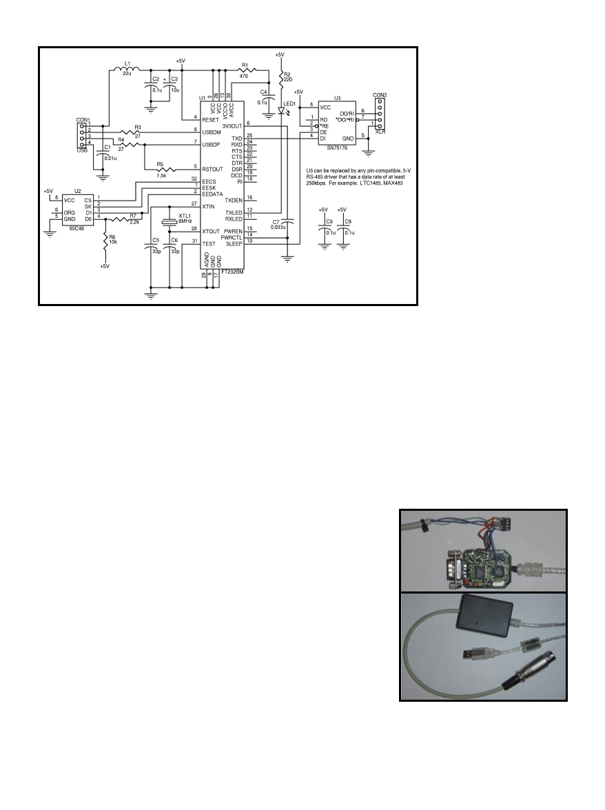
nice, but it works!
The –SLEEP pin connection
is extremely important for com-
plying with the USB specifica-
tion, which explains that a USB
device must consume less than
500 µA in USB Suspend mode.
Without using the –SLEEP pin
to disable the RS-485 driver in
Suspend mode, this condition
can’t be satisfied.
I used standard DMX and USB
cables (see Photo 1b). The red
LED turns on as soon as the PC
sends data.
DMX-512 CONNECTORS
Three different connector
types are normally used for
DMX-512 (see Table 1). As some
designers have reported, the posi-
tive and negative are exchanged
in some equipment (e.g., older
Martin equipment). In case it doesn’t
work with yours, exchanging the posi-
tive and negative might do the trick.
Note that Figure 2 shows the pinout
for the XLR five-pin connector.
DMX-512 REFRESH RATE
Some DMX devices have a built-in
timeout. If more than 1 s elapses
without receiving a DMX signal, they
automatically enter a predefined
standby mode. Therefore, you need to
send the DMX-512 stream periodically.
www.circuitcellar.com
CIRCUIT CELLAR
®
Issue 170 September 2004
73
FT232BM chip, it’s easy to generate the
necessary 250,000 bps when using the
FTDI D2XX DLL USB drivers. In the
past, the standard PC UART’s bit rate
limitation was seemingly one of the
main problems for using it to generate a
DMX-512 signal. Therefore, all existing
DMX-512 interfaces normally have relied
on an additional external microcontroller
that generates the protocol timing.
Use the following data framing of the
FT232BM chip to generate the correct
datastream: 1 start bit, 8 data bits, no par-
ity, and 2 stop bits. The start byte is sent
first. In some special situations, alterna-
tive application-specific start bytes are
defined. But this has to be set to zero
for conventional DMX-512 devices.
After the start byte, send the data
byte for channel 1 followed by chan-
nel 2 and so on. Theoretically, you only
have to send as many channels as
your configuration needs. For example,
if you connect two six-channel dim-
mers, the first dimmer’s DMX start
address is set to one and the second
dimmer’s start address is set to seven.
As a result, you only have to send the
break pulse, start byte ($00), and 12
channel bytes. The Delphi sample soft-
ware always sends all 512 channels, but
you can easily adapt it to your needs.
HARDWARE
The hardware for this project mainly
consists of the FT232BM, which was ini-
tially developed for building simple USB-
to-RS-232 converters (see Figure 2).
[2]
The
chip takes care of handling the USB pro-
tocol. It contains several additional intel-
ligent features: a universal bit rate gener-
ator that can go up to 3 Mbps, RX FIFO,
TX FIFO, and hardware handshaking.
Because of good documentation and
the freely available universal PC driv-
ers, the chip is popular not only for
adding RS-232 ports to legacy-free PC
Systems, but also for other devices
that have to communicate with a PC
or MAC via USB. Therefore, it’s nor-
mally easy to find a chip distributor.
On the other hand, if you don’t feel
like soldering the LQFP-32 yourself,
just do what I did for the prototype: I
bought a USB-to-RS-232 converter
that’s based on the FT232BM chip
(sold by FTDI distributors like Saelig)
and added the RS-485 driver chip and
DMX-512 connector on the fly.
Because the RS-485 driver connects
only to the power supply and two out-
puts of the USB chip, you can leave
the other components on the original
board untouched. As you can see in
Photo 1a, I soldered four wires (VCC,
GND, TXD, and –SLEEP) between the
existing USB-to-RS-232 converter
and the RS-485 chip. I connected the
XLR connector to the RS-485 chip
via three wires. It doesn’t look too
Figure 2—
It doesn’t get any simpler than this. The design consists mainly of the FT232BM chip and an RS-485 line driver.
b)
a)
Photo 1a—
Take a look at the prototype converter. The
PCB was taken from a standard USB-to-RS-232 convert-
er using the FT232BM chip. The chip added on the fly
was the RS-485 line driver SN75176.
b—
The prototype is
in a case. By developing a custom PCB, you can drasti-
cally reduce the size of the case.


www.circuitcellar.com
CIRCUIT CELLAR
®
Issue 170 September 2004
75
By using all 512 channels and the
minimum 88-µs reset time, the protocol
allows you to refresh all the channels at
44 Hz. Tests have shown that because
of break pulse generation and the USB
latency, the maximum refresh rate
achievable with this USB interface and
the PC software is approximately 33 Hz.
This changes slightly from one PC to
another. You can easily test this by
decreasing the TTimer object’s interval.
SOFTWARE
I wrote the PC software in Delphi 5.
However, because you don’t need
fancy components, you should be able
to compile it with any Borland Delphi
version (between 2 and 7). The entire
program control is located in the
main.pas file, which is posted with
the other source files on the Circuit
Cellar
ftp site. The file D2xxUnit.pas
is an object Pascal wrapper for
ftd2xx.dll, which is a slightly modified
and extended version of the one sup-
plied by FTDI.
If you’re unfamiliar with programming
in Borland Delphi, you’ll probably be sur-
prised by the software’s simplicity. It
mainly consists of initialization, an event
handler—which is called every time
you move one of the 12 sliders—and a
TTimer event handler that sends the data
in a predefined period to the USB device.
Let me reiterate that the Delphi code
is extremely simple. With that said, let’s
focus on the USB-related portion of the
four most important routines. I
removed the GUI-related stuff from
Listings 1 and 2.
USB DRIVERS
You may be wondering whether or
not you need to write device drivers.
Don’t worry; it isn’t necessary. FTDI
offers two sets of USB drivers. On one
side is the virtual COM port (VCP)
driver, which installs a VCP. This is
advantageous because it can be
accessed like a normal serial COM
port, but it isn’t suited too well for
this project because the driver by default
supports only the Windows standard RS-
232 bit rates, which normally only go
up to 115,200 bps. The FTDI web site
describes a possible workaround for this
problem, but it seems to be tricky and
not the best option.
The second driver is the D2XX DLL
USB driver, which provides direct access
to the chip via the supplied DLL/driver
combination. This does away with the has-
sles of legacy COM port interfaces. It’s
advantageous because you can easily
program any bit rate including the
required 250,000 bps.
Listing 1—
In the first section (
RefreshBtnClick
), I’m trying to connect to the USB device. If successful, I’ll get and
check the USB-to-DMX converter chip information. The
OpenBtnClick
routine opens the USB link and configures the
USB device to generate the timings according to the DMX-512 specification. The transmission timer is enabled at the end.
procedure TForm1.RefreshBtnClick(Sender: TObject);
// Check if there is an appropriate USB device. If so, display them.
var i : Integer;
ok : boolean;
DeviceCount : DWord;
aDevice_String : Array [1..50] of Char;
SerialNo : String;
Description : String;
begin
// Get number of devices
FT_GetNumDevices(DeviceCount,Nil,FT_LIST_NUMBER_ONLY);
If DeviceCount > 0 then
begin
For I := 0 to DeviceCount-1 do
Begin
// Get the serial number
ok := FT_ListDevices(i,aDevice_String,
FT_OPEN_BY_SERIAL_NUMBER or
FT_LIST_BY_INDEX) = FT_OK;
// Store the serial number
SerialNo := aDevice_String;
// Get the device description
if ok then ok := FT_ListDevices(i,aDevice_String,
FT_OPEN_BY_DESCRIPTION or
FT_LIST_BY_INDEX)) = FT_OK;
// Store the device description
Description := aDevice_String;
if ok then
begin
// Display the serial number and the description of this
device.
end;
End;
end;
end;
procedure TForm1.OpenBtnClick(Sender: TObject);
// Open the selected USB device.
Var Index : Integer;
begin
Index := SelectedDevice;
If FT_Open(Index,FT_Handle) = FT_OK then
Begin
// Reset the chip.
FT_ResetDevice(FT_Handle);
// Define timeouts. (RX timeout is not important for this
// application.)
FT_SetTimeouts(FT_Handle,16,50);
// Set the DMX data rate.
FT_SetBaudRate(FT_Handle,250000);
// Set DMX-512 data characteristics.
FT_SetDataCharacteristics(FT_Handle,FT_DATA_8,
FT_STOP_2,FT_PARITY_NONE);
// Disable handshaking.
FT_SetFlowControl(FT_Handle,FT_FLOW_NONE,FT_XON_Value,
FT_XOFF_Value);
// Restart the Ttimer object.
Timer1.Enabled := True;
end;
end;

76
Issue 170 September 2004
CIRCUIT CELLAR
®
www.circuitcellar.com
you’re properly connected to
the device. Now you can
move the 12 sliders as you see
fit. By setting the start chan-
nel to 25, for example, chan-
nel 1’s slider becomes channel
25, channel 2’s becomes chan-
nel 26, and so on.
The aforementioned pro-
gram is an easy sample. Now it’s up
to your imagination. Think about
some preset buttons and hotkey pre-
sets. By adding TCP/IP functionality
to your Delphi application, you can
also control your light from any PC
via your wireless LAN by connecting
a dimmer pack with this interface to
your server.
POSSIBLE IMPROVEMENTS
My project works well, but you can
make several improvements. For
instance, you can put the
send routine
in a separate Windows thread. With
this, the DMX-512 transmission would
become more independent of the appli-
cation. If you perform a time-consum-
ing task in the main application, the
DMX-512 refresh can be suspended for
some time.
Galvanic isolation is another option.
USB VID & PID
Every USB device needs
specific vendor ID (VID) and
product ID (PID) numbers
programmed into its EEP-
ROM. As soon as you con-
nect the device, the operat-
ing system will use the two
numbers to locate the appro-
priate drivers.
If the FT232 chip discovers an empty
EEPROM connected to the EECS,
EESK, and EEDATA pins, it automati-
cally uses the FTDI VID 0x0403 and the
default PID 0x6001. The standard USB-
to-RS-232 cable I bought for my proto-
type was also programmed to this
FTDI default VID/PID combination.
The USB-to-DMX-512 interface
should work with the default VID/PID
combination, as long as you supply the
correct direct drivers during installation.
But, unfortunately, this could lead to
driver mismatch with other USB devices
containing the same chip. Therefore, you
have to reprogram the EEPROM with the
PID 0xEC70, which has been reserved
for the USB-to-DMX-512 project.
There are different ways to reprogram
the EEPROM. I’ll focus on one option.
At first glance you’ll think it’s a bit
complicated. But after you consider the
different problems you could encounter
with the different Windows versions
(especially XP), it’s the easiest solution.
INSTALLATION
When you connect the device for the
first time, Windows asks for the corre-
sponding device drivers. If you don’t have
the original disks, use the necessary driv-
ers in the VCP driver subfolder posted
on the Circuit Cellar ftp site. Windows
XP will automatically install them.
Next, you must remove the USB
devices that might contain an FTDI
chip using the default VID/PID combi-
nation. If you’re not sure about this,
remove all of the USB devices except
the one you want to reprogram.
Now you can start the USB2DMX512-
Reprogrammer.exe program, which is
posted on the Circuit Cellar ftp site.
After start-up, the status line should be
blank. If you see the “Please connect
the device!” message, it means your
USB device isn’t connected, it isn’t
working properly, or that there is a
problem with the driver installation.
Next, press the “Try to reprogram now!”
button. If everything works, the status line
reads, “Device reprogrammed with
USB2DMX512 PID.” It doesn’t just
reprogram the PID; it also programs the
device name and the maximum allowable
current (90 mA) needed from the USB port.
After disconnecting and reconnecting
(wait several seconds in between) your
device, it will be recognized by Windows
as “USB2DMX512 Converter.” Windows
will then ask for drivers. At this point
you can install the final drivers, which
are located in the USB2DMX512 drivers
subfolder. That’s all! Now you can run
the USB2DMX512.exe file.
If your USB device is properly
installed, you should see it listed in the
top section of the window (see Photo 2).
Select it and click the Open button. If
you don’t receive an error message,
Listing 2—
The
Timer1Timer
procedure is called periodically by the transmission timer. It generates the
DMX-512 reset pulse and sends the 512 channels to the chip.
CloseBtnClick
stops the transmission by
disabling the transmission timer and closing the USB link.
procedure TForm1.Timer1Timer(Sender: TObject);
// Send the DMX stream, triggered by a Ttimer component.
var ok : boolean;
Count : DWord;
Begin
// Stop timer.
Timer1.Enabled := False;
// Generate the DMX break.
ok := FT_SetBreakOn(FT_Handle)=FT_ok;
if ok then ok := (FT_SetBreakOff(FT_Handle) = FT_OK);
// Send the start byte and the 512 DMX-512 channels.
if ok then ok := (FT_Write(FT_Handle,@DMX_Buf,
DMXChannelsMax+1,Count)=FT_ok);
// If we get an error, we stop the transmission, otherwise
restart.
if ok then Timer1.Enabled := True
else CloseBtnClick(Self);
end;
procedure TForm1.CloseBtnClick(Sender: TObject);
// Close the USB device.
Begin
// Stop the DMX refresh.
Timer1.Enabled := False;
// Close the USB device.
FT_Close(FT_Handle);
end;
DMX-512 signal
XLR 3 pin
XLR 5 pin
Stereo Jack 6.5 mm
Ground (shield)
1
1
Sleeve
Data –
2
2
Ring
Data +
3
3
Tip
Second Data – (optional)
4
Second Data + (optional)
5
Table 1—
Here are the pinouts for the most commonly used DMX-512 connectors.
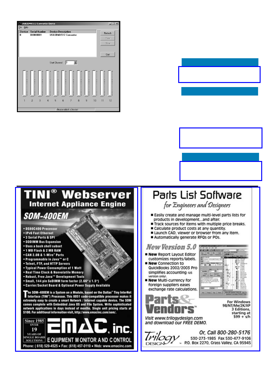
www.circuitcellar.com
CIRCUIT CELLAR
®
Issue 170 September 2004
77
enough to be put in the
“radio frequency” catego-
ry of signals. Therefore,
you need proper termina-
tion. The simple rule is
this: at the end of each
chain of DMX-512
receivers, there should be
a 120-
Ω
termination
resistor between Data +
and Data –. For short
cables, it works without
termination, but it’s
cleaner to add this termi-
nation anyway.
REAL-LIFE TESTS
I’ve used the circuit
with several different
brands of show scanners
and dimmer packs. It worked proper-
ly with all of these devices without a
blackout or any problems. Therefore,
you can be sure that it will also
work with other DMX-512-compati-
ble lighting equipment, such as a
huge 10-kW Space Cannon skylight
fixture.
I
If you use the DMX-512 interface on
stage, the galvanic isolation of the line
driver could improve reliability and
protect your computer against possible
over-voltage on the DMX-512 cables.
DMX-512 TERMINATION
The DMX-512’s data rate is fast
PROJECT FILES
To download the code, go to ftp.circuit
cellar.com/pub/Circuit_Cellar/2004/170.
SOURCE
FT232BM USB UART IC
FTDI, Ltd.
www.ftdichip.com
REFERENCES
[1] USITT, “Entertainment
Technology—USITT DMX512-A
Asynchronous Serial Digital Data
Transmission Standard for Con-
trolling Lighting Equipment and
Accessories Rev. 3,” Draft BSR E1.11.
[2] FTDI, “FT232BM USB UART (USB—
Serial) I.C.,” DS232B, V. 1.4, 2004,
www.ftdichip.com/FTProduct.htm.
Photo 2—
This simple sample application was written in Delphi 5. The top part
lists the available USB-to-DMX-512 devices. The lower part allows you to set the
12 channels. Feel free to adapt and extend it to fullfill your needs.
Stefan Kalbermatter has worked in
Switzerland for more than eight years
as an independent hardware and soft-
ware consultant. You may contact him
via his web page www.kalbermatter.ch.

because they’re the ones pushing the
limits. There’s also the commercial
reality that Wintel dominates the
microprocessor business, sullying the
pure science. When it comes to com-
puter architecture, might—as in $1
billion fabs—makes right. Fortunately,
in the blue-collar embedded space,
there’s still breathing room for com-
puters that don’t all look like they
were designed by, well, computers.
DEDUCE & REDUCE
According to the Maxim marketing
pitch, MAXQ is a family of RISC
microcontrollers targeted toward low-
cost, low-power embedded applica-
tions. Having reviewed all the docu-
mentation, I conclude the MAXQ is,
and isn’t, a RISC. Oh, sure, it is a RISC
in the sense that term has devolved to
mean practically anything that isn’t an
’x86. But, as you’ll see, the MAXQ cer-
tainly isn’t a RISC in the traditional
78
Issue 170 September 2004
CIRCUIT CELLAR
®
www.circuitcellar.com
This is the end, beautiful friend
This is the end, my only friend
The end of our elaborate plans
The end
––The Doors
, “The End,” The Doors,
Elektra/Asylum,
1967.
“Y
es, all seems rosy as the wiz-
ards of microprocessors bed down for
the night. But, perhaps in those dark-
est hours before dawn, do some toss
and turn, unable to shake a feeling
there’s trouble ahead?”
So I wrote back in 1997 in my swan
song for the dying art of computer
architecture (“Architecture is dead?
Long live architecture!” Computer
Design
, 1997). No irony or surprise in
the fact that Computer Design maga-
zine ultimately folded.
The gist of the “architecture is dead”
argument is implementation (i.e.,
faster, denser, and, above all, cheaper
transistors), rather than the way the
transistors are put together, is where the
action is. Indeed, the writing—an obitu-
ary in this case—was on the wall with
the emergence of the “quantitative
approach” to computer design that
sparked the RISC revolution of the early
1980s.
[1]
At that point, computer archi-
tecture became a science, not an art.
That isn’t necessarily a bad thing, but
it sure took the fun out of the subject.
Much as the way the quest for practical-
ity and efficiency have stripped cars of
their individuality, so too we no longer
create novel computer architectures as
in the days of yore. That’s the way the
wind blows, but don’t you sometimes
hanker for some chrome and tailfins?
The high-end super-duper chips are
most subject to architectural angst
sense of the word. And as far as I’m con-
cerned, that’s a good thing. There are
already plenty of theologically semi-pure
RISC-like chips on the market. Besides,
whatever you call it, MAXQ isn’t boring.
To set the stage, let’s contemplate just
how reduced a RISC could be. As
Maxwell Smart used to say, would you
believe one instruction? It’s called a
Turing machine. Computer experts may
be familiar with the concept, but for
those of you who aren’t, a brief history
lesson is in order. My apologies ahead of
time for what is clearly an overly
expeditious and less than rigorous inter-
pretation of Alan Turing’s discovery.
Turing was just 24 years old in 1936
when he published “On Computable
Numbers, With An Application To The
Entscheidungsproblem” (see Photo 1).
Already an elected fellow in the math-
ematics department Cambridge
University, this was just the opening act
in Turing’s short but brilliant career.
[2]
In an abstract sense, the question of
the time was whether there was a
method by which it could be proved
that a particular mathematic proposi-
tion was provable. Turing demonstrat-
ed that the answer is no, which caused
a tizzy in math circles at the time.
But along the way, almost as an
aside, Turing’s work sounded the open-
ing chord of the computing revolution
to come, one that still resonates to this
day. In particular, he showed that while
not everything is computable, every-
thing that can be computed could be
computed by a simple machine.
The archetypal Turing machine is
comprised of a tape (infinite length to
keep things simple) and a processor that
is reduced indeed. All it can do is read or
A Simple Plan
SILICON UPDATE
by Tom Cantrell
Is the MAXQ a RISC, CISC, or something in-between? According to Tom, it doesn’t matter.
What is important is that the MAXQ is becoming increasingly competitive in the MCU market.
Photo 1—
Many think RISC is a recent trend, but Alan
Turing’s (1912–1954) Turing machine was really reduced.
It set the stage for all the digital computers that followed.

www.circuitcellar.com
CIRCUIT CELLAR
®
Issue 170 September 2004
79
write a zero, one, or blank (i.e., erase) on
the tape and move the tape left or right.
Thus, the single instruction the machine
can execute boils down to the following:
CURRENT_STATE, CURRENT_SYMBOL,
NEW_STATE, NEW_SYMBOL, LEFT/RIGHT
The machine examines the CUR-
RENT_SYMBOL under the read/write
head. Depending on the result and the
CURRENT_STATE, the machine enters
a NEW_STATE, writes a NEW_SYM-
BOL (zero, one, or blank), and moves
the tape one position to the left or right.
There are a lot of virtual Turing
machines on the ’Net. I will turn to
one of them for a simple example
(www.nmt.edu/~prcm/turing/vtm.cgi.)
Let’s say you want to add two num-
bers, each represented as a string of
ones of length one greater than the
magnitude. To add two and one,
start with a tape that looks like the
following:
_<1>1 1 _ 1 1 _ //‘111’ is 2,
‘11’ is 1
You end up with:
_ 1 1 1 1 _<_>_ //sum is
‘1111’ i.e. 3
Listing 1 shows the program and
step-by-step execution. Yes, this is a
toy example; but, remarkably, with
the proper instructions (or “table of
behavior,” in Turing’s words), a Turing
machine can do anything a real com-
puter can. You can even run Windows
on a Turing machine!
Turing himself would soon embark
on another intellectual adventure in
the bowels of Bletchley Park during
World War II, when he was chal-
lenged—and prevailed—in a quest to
crack the German Enigma encryption
scheme. It’s such a great story, it was
the basis (but little more than that) for
a movie of the same name, Enigma
(Manhattan Pictures, 2002). The
movie is tech-lite and pure fiction in
many respects, but there’s at least a
passing reference to Turing’s work and
his “thinking machine.”
It’s no surprise that Turing contin-
ued after the war to make his mark
during the development of the earliest
digital computers. As if that wasn’t
enough, he pioneered the concept of
artificial intelligence with his Turing
test, which remains to this day the
hurdle computers must leap before they
can aspire to replace their masters.
Unfortunately, Turing’s story doesn’t
have a happily ever after Hollywood
ending. In 1954, he was found dead in
his room along with a half-eaten
cyanide-laced apple. (It was ruled a sui-
cide, although some people wonder.)
SISC?
Turing, in fact, proved that a com-
puter with a single instruction (some-
thing along the lines of MEMORY-TO-
MEMORY SUBTRACT-AND-
BRANCH-NEGATIVE) is entirely pos-
sible, although not especially useful.
But there are more practical examples,
such as the class of computers some-
times referred to as move machines.
[3]
In this scheme, processing is accom-
plished by explicitly moving data to
and from functional units. For
instance, instead of an ADD or SHIFT
instruction, the program would MOVE
data to an ADDER or SHIFTER. In
essence, it simply replaces an instruc-
tion decoder with an address decoder.
If you’re wondering, this finally
brings me back to the subject at
hand—namely, the MAXQ’s transport
triggered architecture. The unique
aspects are hidden behind the rather
mild-mannered facade of a middle-of-
the-road MCU with accumulators,
data pointers, bit operations, and a
64-KB (x16) address space. There are
multiple accumulators (from eight to
16 depending on implementation), but
only one is live (selected by an accu-
mulator pointer register) at any given
time. There are also specialized regis-
ters (e.g., loop counters) that don’t fit
the general-purpose register philoso-
phy. However, MAXQ lives up to the
load/store tenet of RISC in that
instructions generally operate only on
the accumulator.
Go underneath the seemingly con-
ventional assembly language veneer,
and you’ll find that the architecture is
built on a single-instruction format (see
Figure 1 and Table 1). In this regard,
MAXQ definitely stands out from the
crowd because even the simplest CPUs
Listing 1—
Though a toy example, this “table of behavior” (i.e., program) for adding two numbers on a Turing
machine demonstrates how a simple machine can do complicated things
// This is a small script for adding two numbers that are
// represented by a string of 1s with a length of one more
// than the number. The numbers have a blank separating them
// and a blank at the end.
pass_1, 1, pass_1, 1, R // get past the first number
pass_1, _, pass_2, 1, R // change the middle _
pass_2, 1, pass_2, 1, R // get past the second number
pass_2, _, delete1, _, L // end of second number, start back
delete1, 1, delete2, _, L // delete the last 1, go back
delete2, 1, HALT, _, R // delete the second to last 1
_<1>1 1 _ 1 1 _ // pass_1
_ 1<1>1 _ 1 1 _ // pass_1
_ 1 1<1>_ 1 1 _ // pass_1
_ 1 1 1<_>1 1 _ // pass_1
_ 1 1 1 1<1>1 _ // pass_2
_ 1 1 1 1 1<1>_ // pass_2
_ 1 1 1 1 1 1<_> // pass_2
_ 1 1 1 1 1<1>_ // delete1
_ 1 1 1 1<1>_ _ // delete2
_ 1 1 1 1 _<_>_ // HALT
Format Destination
Source
f
1
0
ddd dddd
Index module
Index module
Immediate byte data
(i.e., 00h-FFh)
Index module
SSSS SSSS
Figure 1—
The MAXQ transport-triggered architecture
distills instructions into a single format, with source and
destination rather than various instruction formats and
opcodes, defining operation.


three 16-bit words total). Not
unexpectedly, the usual sus-
pects (long branches and calls,
16-bit constants, and second-
ary register accesses) consume
more than one word and one
cycle. Your mileage may vary,
but after poring through the
listing for an assembly lan-
guage demo program, I came
up with an average of about
1.25 words (20-bits) per
instruction.
Variable-length instructions
are supposedly a RISC no-no.
But that doesn’t bother me
much because I was never
fully enamored with the wis-
dom that says every instruc-
tion deserves as many bits as
any other. Furthermore, a
fixed-size instruction is gener-
ally only a feasible option for
larger processors (e.g., 32-bit);
otherwise, there just isn’t
enough shoulder room to take
care of business. Anyway, take
a close look at the fine print
for many so-called RISCs, and
you’ll find that a truly fixed length
instruction machine is more of a rari-
ty than the rule.
Pipelining is another RISC must-
have that MAXQ eschews. Pipelining
(and the cache that invariably goes
with it) is indeed mandatory if per-
formance at any price is the goal. But
why should applications with modest
performance demands pay a price (cir-
cuit complexity, power consumption,
EMI, and the hazards for the compiler
to avoid) for a benefit (peak MIPS) that
they just don’t need in the first place?
Without pipelining, the MAXQ
clock rate is limited to 16 MHz, which
is fine. The last thing an embedded
system needs is a noisy, power-con-
suming, high-speed clock. Indeed, the
Q in MAXQ stands for “quiet.” (The
low-clock rate not only reduces system
EMI, but also minimizes disruption to
on-chip analog functions.) Despite the
lack of pipelining, performance is
decent with most instructions execut-
ing in a single clock (the exceptions
are long branches and the aforemen-
tioned prefixing), thereby delivering
near MIPS-per-MHz throughput.
modify the data pointer value as well.
MAXQ might appear to have a
fixed-length (16-bit) instruction set,
but not quite. In order to deal with
larger address and immediate fields, a
prefix instruction supplies the extra
bits. For example, a short branch (rela-
tive 8-bit offset) fits in a single 16-bit
instruction, but a long jump (absolute)
goes like this:
//Jump to 16-bit address #1234h
MOVE PFX[0},#12h
JUMP #34h
Note that a loaded prefix is only
valid for the immediately following
instruction. Subsequently, the prefix
register contents revert to zero, so you
can’t load it now and use it later. The
MAXQ avoids a possible gotcha by
masking interrupts between the adja-
cent load and use of a prefix register.
Most instructions will indeed
require just one 16-bit word, but that’s
upped to two whenever a prefix is
required. Indeed, there are even special
cases (likely, and fortunately, very
rare) that call for two prefixes (i.e.,
typically include at least a few instruc-
tion formats. Furthermore, there are
only three addressing modes (Direct,
Indirect, and Immediate). Conceptually,
at least, MAXQ instructions are more
about sources and destinations than
opcodes and addressing modes.
The
MOVE instruction provides the
best example. Every CPU (and periph-
eral) resource is mapped to the address
space. However, actually writing a
program with just
MOVE instructions is
a little awkward, which is why the
MAXQ assembler fronts a more con-
ventional repertoire. But under the
hood, a MAXQ branch instruction is
actually a move to the instruction
pointer, which is just a register like
any other.
Similarly, instead of special auto-
increment and -decrement addressing
modes, MAXQ delivers that function-
ality via different alias addresses of the
data pointer register. In other words, a
move to one location (e.g., @DP) access-
es memory via a data pointer without
modification. Move to another loca-
tion (e.g., @++DP), and you access
memory via the same data pointer but
Mnemonic
Description
Mnemonic
Description
Bit manipulation
Logical
MOVE C, #0/#1
Clear/set carry
AND
Logical AND
CPL C
Complement carry
OR
Logical OR
AND Acc.<b>
Logical AND carry with accumulator bit XOR
Logical XOR
OR Acc.<b>
Logical OR carry with accumulator bit
CPL, NEG
One’s, two’s complement
XOR Acc.<b>
Logical XOR carry with accumulator bit SLA, SLA2, SLA4
Shift left arithmetically 1,
2, 4
MOVE C, Acc.<b>
Move accumulator bit to carry
SRA, SRA2, SRA4 Shift right arithmetically 1,
2, 4
MOVE Acc.<b>, C
Move carry to accumulator bit
SR
Logical shift right
MOVE C, src.<b>
Move register bit to carry
RR, RRC
Rotate right carry
(ex/in)clusive
MOVE dst.<b>, #0/#1
Clear/set register bit
RL, RLC
Rotate left carry
(ex/in)clusive
Math
Data transfer
ADD, ADDC
Add carry (ex/in)clusive
XCHN
Exchange accumulator
data nibbles
SUB, SUBB
Subtract carry (ex/in)clusive
XCH (MAXQ20)
Exchange accumulator
data bytes
Flow control and branching
MOVE dst, src
Move source to destination
JUMP {C/NC/Z/NZ/E/NE/S} Jumps—unconditional or conditional,
PUSH/POP
Push/pop stack
relative, or absolute
DJNZ LC[n], src
Decrement counter, jump not zero
POPI
Pop stack and enable
interrupts (INS
≤
0)
CALL
Call—relative or absolute
Other
RET {C/NC/Z/NZ/S}
Return—unconditional or conditional
NOP
No operation
RETI {C/NC/Z/NZ/S}
Return from interrupt—unconditional
CMP
Compare with accumulator
or conditional
www.circuitcellar.com
CIRCUIT CELLAR
®
Issue 170 September 2004
81
Table 1—
Underneath a mild-mannered assembly language facade, MAXQ uses a novel transport-triggered architecture.

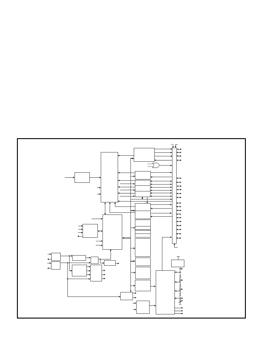
www.circuitcellar.com
CIRCUIT CELLAR
®
Issue 170 September 2004
83
REALITY SHOW
With 8- (MAXQ10) and 16-bit
(MAXQ20) versions on tap, the
MAXQ architecture is capable of serv-
ing as the basis for a broad family of
low-end and mid-range parts. First up
is the MAXQ2000, a 16-bit version
with a built-in LCD driver suitable for
a wide variety of applications, espe-
cially battery-powered hand-held gadg-
ets (see Figure 2). With a low-voltage
1.8-V core (3-V I/O), power consump-
tion is minimal, on the order of 2 mA
per megahertz active and a few
microamps in standby.
Beyond the LCD controller, which
can handle up to 132 segments (i.e.,
four COM and 33 SEGMENT pins),
the part includes a full complement of
peripherals. The three 16-bit program-
mable timer/counters and two UARTs
reminded me of those on an 8051,
although suitably modernized. Perhaps
that’s no surprise considering that
Dallas-now-Maxim still has a stable
full of fancy-’51 MCUs. More histori-
cal roots are found in the built-in 1-
Wire interface, a clever scheme invent-
ed by Dallas. SPI, a real-time clock,
and a watchdog timer round out the
list of usual suspects.
DSP aficionados and number
crunchers take note. This particular
part has a single-cycle 16 × 16 multi-
plier with 40-bit accumulator. That’s a
pretty lot of math horsepower for an
otherwise entry-level MCU.
As for memory, the ’2000 includes
32 KB × 16 of flash memory and 1 KB ×
16 of RAM arranged in a Harvard
architecture with separate buses for
the flash memory and SRAM. A vari-
ety of memory-mapping modes bridge
the gap, for example mapping flash
memory to data space (e.g., look-up
table, in-system programming) and
RAM to program space (e.g., to exe-
cute code located in RAM).
There’s also a 4 KB × 16 utility
ROM with routines for initializing the
flash memory and accessing on-chip
debug hardware via a JTAG interface.
The debug hardware includes program
and data breakpoint registers as well as
the ability to single-step the processor.
The 16-level hardware stack is
almost surely not enough for general-
purpose use and best remains dedicat-
ed to interrupts and subroutine call
and return addresses. For more exten-
sive use (e.g., C compiler, recursive
algorithms), plan on implementing a
software stack.
Watchdog
timer
WDCLK
WDINT
Interrupt
controller
SYS_AL
DAY_AL
3WINT
Three/four-
wire (SPI)
interface
SS
SCLK
MOSI
MISO
1-Wire
interface
Timer0
1WINT
T0INT
T0CLK
T1INT
Timer1
Timer2
T2INT
T2CLK
WKUP
WKOUT_EN
WK_OUT
OWOUT
OWIN
T0
T0B
T1
T1B
T2
T2B
16-bit
RISC CPU
Emulation
download
P4.0/TCK/INT8
P4.1/TDI/INT9
P4.2/TMS
P4.3/TDO
VDDCPPU
RESET
GND
HF
OSC
32k
OSC
HFXIN
HFXOUT
32KIN
32KOUT
SCLKDIV
HFCLK
TCLKDIV
2:1
MUX
3
2:1
MUXES
T0CLK
T1CLK
T2CLK
WDDIV
SYSCLK
WDCLK
Serial
UART1
Serial
UART2
IOINT
TXD0
RXD0
TXD1
RXD1
Register
file
DPTR0
DPTR1
DPTR2
32K × 16
(64 KB)
Flash ROM
or
mask ROM
2k × 8
RAM
16 × 16
HW
Multiply
17 × 8
LCD
RAM
RTC and
alarms
LCD
CLK
Selection
132-Segment
LCD
controller
driver
LCD Bias
control
32 kHz
HF OSC/128
LCD
CLK
VLCD
VDDIO
P5.4/SS
P5.5/MOSI
P5.6/SCLK
P5.7/MISO
P6.4/T0/WKOUT
P6.5/T0B/WKOUT
P6.1/T1/INT13
P6.0/T1B/INT12
P6.3/T2/OWIN
P6.2/T2B/OWOUT
P7.0/TX0/INT14
P7.1/RX0/INT15
P5.3/TX1/INT11
P5.2/RX1/INT10
SEG[28:31]/P3[4:7]/INT[4:7]
SEG[24:27]/P3[0:3]
SEG[16:23]/P2[0:7]
SEG[8:15]/P1[0:7]
SEG[0:3]/P0[0:3]
SEG[4:7]/P0[4:7]/INT[0:3]
GND
VLCD
VLCD1
VLCD2
VADJ
GNDIO
SEG[32]/INT16
COM[0]
COM[3:1]/SEG[33:35]
MAXQ2000F
68QFN (10 mm × 10 mm)
32K
CLK
U1INT
U2INT
T1CLK
SYS_AL
DAY_AL
VDDIO
P
ad dr
iv
ers
Figure 2—
The first implementation of the MAXQ architecture, the MAXQ2000, incorporates an LCD controller to serve in a variety of hand-held battery-driven applications.
Low-power applications are a good match considering the parts capability to deliver multiple MIPS per milliamp.
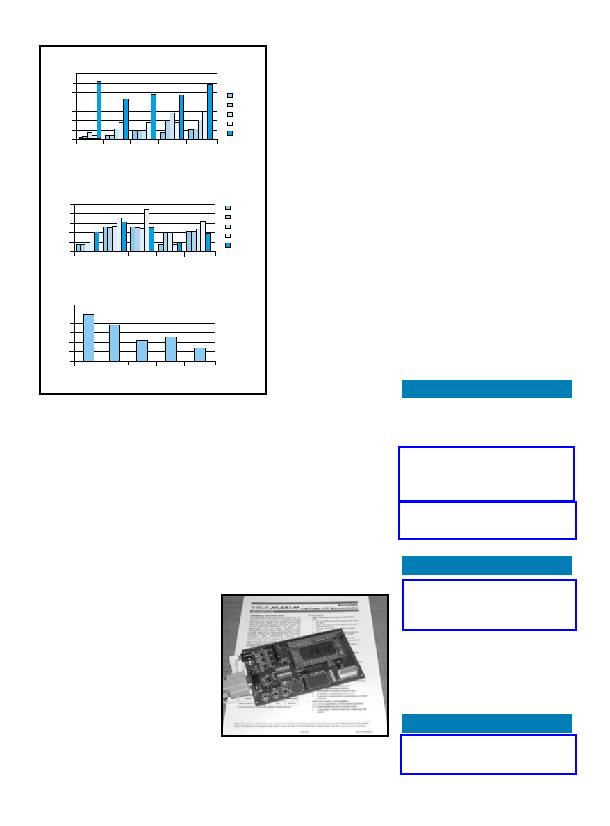
84
Issue 170 September 2004
CIRCUIT CELLAR
®
www.circuitcellar.com
BENCHMAX
The MAXQ folks have cranked up
some benchmarks to make their case
(see Figure 3). For more information
on the subject, refer to Maxim’s
“Introduction to the MAXQ
Architecture” listed in the Resources
section at the end of the column.
Of course, when it comes to bench-
marks, the watchword is “buyer
beware.” For example, one of the rou-
tines is a memory copy, one that just
happens to assume an even number of
bytes and word alignment, giving a big
advantage to a 16-bit chip. Fairness
prevails because the benchmark
includes both 8- and 16-bit versions of
MAXQ. Yes, the 16-bit MAXQ20 is
much faster at word-aligned memory
transfers than an 8-bit chip, including
an 8-bit MAXQ10.
Also note that the report measures
benchmark speed in terms of cycles,
handicapping the real-time results for
processors that support
higher frequency opera-
tion than MAXQ. And
for those of you plan-
ning to use C language,
these assembly language
benchmarks don’t
address the fact that a
good machine can be
easily hobbled by a bad
compiler and vice versa.
Nevertheless, the
results demonstrate that
the MAXQ is no slouch.
Who cares whether it’s a
RISC, CISC, or some-
thing in-between? The
bottom line is that
MAXQ appears to be a
worthy contender and
competitive with all the
other popular players in
the mainstream MCU
market.
SUMMARY
A brand new core in
the 8-bit world, no less
from an outfit with the
combined credentials of
Maxim and Dallas, is
pretty big news. If it
seems like I’ve breezed
through it, it isn’t
because it isn’t a good story, but
rather that it’s only half the story. Of
course, an acceptable architecture is a
must—but so are good tools, market-
ing, and support (see Photo 2).
Furthermore, just as today’s high-
end chip CPU story is more about
adding extra cache than obsessing
over architectural frills, so it is in the
MCU space. The stuff around the
processor core is as important (or even
more) than the details of the processor
itself. Yes, the MAXQ architecture is
interesting, but so are the prospects
for integrating add-on peripheral func-
tions of all sorts. Just take a look at
the Maxim catalog, and you’ll see
there’s no shortage of potential
matchups.
Computer architecture may be a sci-
ence, but crafting embedding systems
remains the art of cleverly applying
the latest and greatest technology to
make a pretty picture. The best
designs are never boring shades of
gray, and a chip like MAXQ may be
just the thing to add a dash of color to
your palette.
I
Photo 2—
The MAXQ evaluation board comes with a
plug-in LCD module (the MCU is hidden under the
LCD) and a serial-to-JTAG converter board.
35,000
30,000
25,000
20,000
15,000
10,000
5,000
MemCp
y64
Bub
bleSor
t
He
x2
Asc
ShiftRt2
BitBang
Cycles
Cycle count
MAXQ20
MAXQ10
AVR
MSP430
PIC16Cxx
50
40
30
20
10
0
MemCp
y64
Bub
bleSor
t
He
x2
Asc
ShiftRt2
BitBang
Bytes
Byte count
MAXQ20
MAXQ10
AVR
MSP430
PIC16Cxx
1.2
1
0.8
0.6
0.4
0.2
0
MAXQ20
MAXQ10
AV
R
MSP430
PIC16C
xx
W
o
rk/po
w
e
r
Work/power (i.e., normalized MIPS/mA)
0
Figure 3—
Even with a grain of salt, benchmarks demonstrate that MAXQ
can play in the MCU big leagues. Performance
(a)
and code density
(b)
are
the usual metrics. Normalizing the number of instructions required to complete
a task and multiplying by MIPS/mA provides a measure of work delivered
for power consumed
(c)
, a surrogate for battery life in portable applications.
c)
b)
a)
Tom Cantrell has been working on chip,
board, and systems design and marketing
for several years. You may reach him by
e-mail at tom.cantrell@circuitcellar.com.
REFERENCES
[1] J. Hennesy, et al., Computer
Architecture: A Quantitative
Approach
, Morgan Kaufmann, San
Francisco, 2002.
Stanford Encyclopedia of Philosophy,
plato.stanford.edu/archives/sum2002
/entries/turing/.
[3] D. W. Jones, “The Ultimate RISC,”
www.cs.uiowa.edu/~jones/arch/
risc/.
RESOURCES
pdfserv.maxim-ic.com/en/ej/MER_3.pdf.
A. Turing, “On Computable Numbers,
With An Application To The
Entscheidungsproblem,” Proceedings
of the London Mathematical Society,
series 2, vol. 42, 1936.
SOURCE
www.circuitcellar.com
CIRCUIT CELLAR
®
Issue 170 September 2004
85
IDEA BOX
THE
DIRECTORY
OF
PRODUCTS AND
SERVICES
AD FORMAT
: Advertisers must furnish digital submission sheet and digital files that meet the specifications on the digital submission sheet.
ALL TEXT AND OTHER ELEMENTS MUST FIT WITHIN A 2
″″ ××
3
″″
FORMAT
. Call for current rate and deadline information. Send your disk and digital submis-
sion sheet to: IDEA BOX, Circuit Cellar, 4 Park Street, Vernon, CT 06066 or e-mail kc@circuitcellar.com. For more information call Sean Donnelly at (860) 872-3064.
The Suppliers Directory at www.circuitcellar.com/suppliers_dir/
is your guide to a variety of engineering products and services.
86
Issue 170 September 2004
CIRCUIT CELLAR
®
www.circuitcellar.com

www.circuitcellar.com
CIRCUIT CELLAR
®
Issue 170 September 2004
87

88
Issue 170 September 2004
CIRCUIT CELLAR
®
www.circuitcellar.com
www.circuitcellar.com
CIRCUIT CELLAR
®
Issue 170 September 2004
89

90
Issue 170 September 2004
CIRCUIT CELLAR
®
www.circuitcellar.com

www.circuitcellar.com
CIRCUIT CELLAR
®
Issue 170 September 2004
91

92
Issue 170 September 2004
CIRCUIT CELLAR
®
www.circuitcellar.com

www.circuitcellar.com
CIRCUIT CELLAR
®
Issue 170 September 2004
93

Intelligent Sensor Head
E-Field Serial Touchpad
Telephone Message Watchdog: An Intelligent Call-Forwarding System
Pseudo-Random Noise Generator: Theory and Applications
Single-Board Logic Analyzer
ABOVE THE GROUND PLANE
Stepper Driver (Part 2): Digital
APPLIED PCs
Big PICs
FROM THE BENCH
Digital Radio Control
SILICON UPDATE
Try Hard with a Vengeance
94
Issue 170 September 2004
CIRCUIT CELLAR
®
www.circuitcellar.com
89
Abacom Technologies
92
Acacetus
93
All Electronics Corp.
88
Animated Lighting, L.C.
52
AP Circuits
45
Arcom
89
Ash Ware, Inc.
7
Atmel
91
Bagotronix, Inc.
44
Bellin Dynamic Systems, Inc.
38
Belsoft
58
Beta Layout Ltd.
28
Bitscope Designs
66
CadSoft Computer, Inc.
87
Carl’s Electronics
44
CCS-Custom Computer Services
92
Conitec
95
CTIA Wireless
85
Cyberpak Co.
15
Cypress Contest
1
Cypress MicroSystems
65
CWAV
91
DataRescue
85
Decade Engineering
85
Digital Creation Labs Inc.
86
Digital Products Co.
85
DLP Design
12
Earth Computer Technologies
The Index of Advertisers with links to their web sites is located at www.circuitcellar.com under the current issue.
Page
90
EE Tools
(Electronic Engineering Tools)
77
EMAC, Inc.
43
Entrelogic Corporation
25
ExpressPCB
85
FDI-Future Designs, Inc.
87
Fitzhugh & Waggoner, Inc.
92
Front Panel Express
37
Future Electronics
89
Grid Connect
86
Hagstrom Electronics
63
HI-TECH Software, LLC
27
Holmate Semiconductor, Inc.
14
ICOP Technology, Inc.
89
IMAGEcraft
61
Imagine Tools
93
Information Analytics
52
Intec Automation, Inc.
93
Integrated Knowledge Systems
91
Intrepid Control Systems
90
Intronics, Inc.
89
Ironwood Electronics
9
Jameco
64, 86
JK microsystems, Inc.
44
JR Kerr Automation & Engineering
13
Kg Systems, Inc.
49
LabJack Corp.
49
Lakeview Research
91
Lawicel HB
39
Lemos International
2
Link Instruments
26, 30
Linx Technologies
10
MaxStream
88
MCC (Micro Computer Control)
90
Microcontroller Services
92
microEngineering Labs, Inc.
88
MJS Consulting
90
Mosaic Industries, Inc.
31
Mouser Electronics
74
MVS
86
Mylydia, Inc.
C2
NetBurner
87
OKW Electronics, Inc.
92
Ontrak Control Systems
30
PCBexpress
87
PCB Fab Express
60
PCBpro
C4 Parallax, Inc.
85
Phytec America LLC
87
Phyton, Inc.
90
Picofab, Inc.
93
Pulsar, Inc.
88
Quality Kits & Devices
86
Quantum Composers, Inc.
87
R2 Controls
71
R4 Systems, Inc.
24
Rabbit Semiconductor
Page
Page
Page
88
Radiotronix
10
Reach Technology, Inc.
13
Remote Processing
57
R.E. Smith
82
RoboNexus
93
Rogue Robotics Corp.
89
Scidyne
3
Scott Edwards Electronics, Inc.
88
Sealevel Systems
5
Sierra Proto Express
11
Silicon Laboratories, Inc.
91
Softools
49
Systronix
90
TAL Technologies
C3
Tech Tools
16, 17
Technologic Systems
87
Technological Arts
90
Tern, Inc.
86
Trace Systems, Inc.
91
Triangle Research Int’l, Inc.
77
Trilogy Design
21
Tri-M Systems Inc.
93
Weeder Technologies
80
Wescon
91
Zanthic Technologies, Inc.
53
Zilog, Inc.
29
Z-World
November Issue 172
Deadlines
Space Close: September 10
Material Due Date: September 20
Theme:
Internet & Connectivity
A
TTENTION
A
DVERTISERS
e-mail: sean@circuitcellar.com
INDEX OF ADVERTISERS
Preview of October Issue 171
Theme: Data Aquisition


I
love it when a good plan comes togethera great sponsor, plenty of interest, and superlative results. Thats exactly how Id describe our
latest Atmel AVR design contest. In fact, this contest has the distinction of being Circuit Cellars most successful contest yet. No doubt youll
agree when you review the most noteworthy projects.
Notice I didnt just say winning projects. Getting a positive result from submitting a project to our contests has very little to do with the
legalese in the contest rules that describes the numerical odds of winning. The real profit for anyone submitting a project is the potential pub-
licity and celebrity that comes from having your entry chosen to be posted or published by Circuit Cellar and Atmel as a significant engineer-
ing design example. The distinction is that this resume-building exposure cant be purchased. It has to be earned, and thats what makes it
unique.
Sifting through the contest projects is not an easy task. Paid professionals do the actual judging, specifically because there is a lot of money
on the line and contestants expect that we do it right. Judges are given the responsibility of deciding project relevance in 20% divisions of tech-
nical merit, originality, usefulness, cost-effectiveness, and design optimization. Ive never been comfortable doing that kind of judging myself.
I prefer my tried-and-true gut scrutiny approach. Basically, I know when I read a good manuscript or see a good project. I dont have to over-
analyze why or explain it to anyone else. I guess that means I can own a magazine, but I better forget being a contest judge.
The good news is that we both get to do our things in these contests. The judges get to pick the official winners, and I get to talk to a lot
more entrants (the unofficial winners) about posting and publishing opportunities. The net result is that many dozens of entrants are involved
in the process, not just a few top-prize winners. Circuit Cellars motive in administering contests isnt just about distributing prize money for
sponsors. Its about cultivating the abundance of engineering talent attracted to contests. Todays contest participant is tomorrows author.
As you might have guessed, deciding which projects deserve to be published is more difficult when we have a very successful contest, but
I still enjoy the challenge. As I write this, the Atmel AVR 2004 Design Contest winners havent been chosen yet, but Ive already started gen-
erating my list of projects that will be named Distinctive Merit. Im just glad I dont have to decide a pecking order because some of these proj-
ects are truly unique (in my completely biased and warped opinion).
For example, one entry is the Traffic Data Display. This tablet-sized device is configured with 512 bicolor LEDs organized as a lighted map
of the L.A. freeway system. Its meant to be used in public service vehicles, buses, emergency response vehicles, cabs, etc. to provide a real-
time display of traffic conditions and tie-ups. The LED display matrix, which receives an ASCII message of map position coordinates via an
alphanumeric pager with FLEX protocol, signifies specific road conditions by color and frequency.
This time around I give the cinematographic highlights award to an industrious cribbage player from Stanford University. The entry called
The Wedding Board is about the construction of an electronic cribbage board, but it also includes a movie about the construction techniques
that borders on the quality of something typically presented at the Cannes Film Festival. I certainly applaud such inventiveness. Of course, a
short video on how to play cribbage wouldnt have hurt either.
In the category of whos explaining this one to Atmel when they read the project title on the list I send at the contest conclusion?, we have
the SIR Sucks A Lot project. I know you guys like making me squirm when I try to tell sponsors that not all of my readers are completely off-
the-wall. For this project, I will explain that its an autonomous robot that collects rice in a floor layout resembling the average living room. The
robot was designed to compete in a household robot vacuum cleaner competition, where the goal was to pick up as much rice as possible in
4 min. Be kind, guys. Atmel is OK, but some sponsors dont have a sense of humor. ;-)
The list goes on and on. We have a Net radio receiver, a 32-channel R/C servo controller, a wireless model rocket launch control system,
a differential scanning calorimeter, a wireless telemetry system for a Formula 1 race car, a data encryption device, a septic tank level monitor,
and more. Rest assured, I will have my work cut out for me triaging the Atmel contest list.
The Most Success Yet
steve.ciarcia@circuitcellar.com
96
Issue 170 September 2004
CIRCUIT CELLAR
®
www.circuitcellar.com
by Steve Ciarcia, Founder and Editorial Director
PRIORITY INTERRUPT

Wyszukiwarka
Podobne podstrony:
circuit cellar1996 09
circuit cellar2004 09
circuit cellar1995 09
circuit cellar1997 09
circuit cellar2000 09
circuit cellar1993 09
circuit cellar2001 09
circuit cellar2002 09
circuit cellar2003 09
circuit cellar1994 09
circuit cellar1996 09
circuit cellar2003 09
circuit cellar1994 09
circuit cellar1997 09
circuit cel1096/5369
więcej podobnych podstron