The Golden Issue?
to our fiftieth issue! When we started
this as a
bimonthly with no ads back in
1988, never would have dreamed I’d see the fiftieth
issue go out the door as a 96-page monthly with a group
of dedicated advertisers and tens of thousands of faithful readers. As a
bonus, we’ve filled this issue with five feature articles plus our regular
columns to make number 50 a bang-up issue. Thanks to our authors and
readers, we can continue to bring you first-class material each month. Here’s
to another 50.
Continuing in the Circuit Cellar tradition of treading into new areas, I’m
pleased to announce that starting with the January ‘95 issue, we will be put-
ting out a quarterly special entitled Home Automation and Building Control.
won’t be just another glossy production that talks down to naive
consumers nor will it cover $50,000 installations in multimillion-dollar homes.
What we will be covering is home automation technology that you can apply
to your own home, whether it be off-the-shelf products, installation
techniques, design ideas, or complete projects. We will also be looking at
the commercial building control side to find out what is happening in that
sector and how it might also be applied to the home. You’ve come to expect
Circuit Cellar to get down to the nitty-gritty and tell it
is, and
won’t be an exception. There is no such thing as “too technical” when it
comes to our readers, so we won’t be holding anything back.
If you are already a regular reader of the Computer Applications
Journal, you don’t have to do anything special to receive
It will be
included in the center of the January, April, July, and October 1995 issues of
CAJ.
In the meantime, I’m looking for authors to write about all aspects of
the home automation industry. Whether it be your experiences with an
the-shelf product, your own design, or tricks of the trade, we want to hear
from you. While we may use the Circuit Cellar HCS as the basis for some
projects we write about here, we want to cover all systems currently on the
market. Unlike some other industry magazines that only seem to recognize
control systems advertised in their pages, we will be providing an equal,
unbiased platform for all to use.
Home automation always a popular topic among our readers (and I
know it’s popular among our staff). However, it still suffers from lack of
consumer awareness and lack of decent user interfaces. It’s all of our
we the pioneers-to help set the stage for acceptance by the masses. A lot
of work needs to be done before that can happen, though. We strive to be
the medium to carry that work, but we still need your help to fill it. Feel free
to contact me with your ideas by E-mail at
or
using any of the other methods listed on page 6.
This should be fun....
2
Issue September 1994
The Computer Applications Journal
CIRCUIT CELLAR
COMPUTER
APPLICATIONS
JOURNAL
FOUNDER/EDITORIAL DIRECTOR
Steve Ciarcia
EDITOR-IN-CHIEF
Ken Davidson
TECHNICAL EDITOR
Janice Marinelli
ENGINEERING STAFF
Jeff Bachiochi Ed Nisley
WEST COAST EDITOR
Tom Cantrell
CONTRIBUTING EDITORS
John Dybowski Russ Reiss
NEW PRODUCTS EDITOR
Harv Weiner
ART DIRECTOR
Lisa Ferry
GRAPHIC ARTIST
Joseph
CONTRIBUTORS:
Jon Elson
Tim
Frank Kuechmann
Kaskinen
PUBLISHER
Daniel Rodrigues
PUBLISHER’S ASSISTANT
Sue Hodge
CIRCULATION COORDINATOR
Rose
CIRCULATION ASSISTANT
Barbara
CIRCULATION CONSULTANT
Gregory Spitzfaden
BUSINESS MANAGER
Jeannette Walters
ADVERTISING COORDINATOR
Dan Gorsky
CIRCUIT CELLAR INK, THE COMPUTER
JOURNAL
published
monthly by
Cellar Incorporated, 4 Park Street.
20, Vernon, CT 06066 (203)
Second
One-year (12 issues)
rate U.S.A. and
tries $49.95. All subscription orders payable in
funds only, via
postal money order
check drawn on U.S. bank. Direct subscription orders
and subscription related
to The Computer
Journal
P.O. Box 696,
Holmes, PA 19043.9613 or call (600)
POSTMASTER, Please send address changes The
Journal,
Dept
Box 696, Holmes, PA
Cover Illustration by Bob Schuchman
PRINTED IN THE UNITED STATES
ASSOCIATES
NATIONAL ADVERTISING REPRESENTATIVES
NORTHEAST
MID-ATLANTIC
Barbara Best
741-7744
Fax: (908)
SOUTHEAST
Collins
(305) 966-3939
Fax: (305) 985-8457
MIDWEST
Nanette Traetow
WEST COAST
Barbara Jones
Shelley Rainey
(714) 540-3554
Fax: (714) 540-7103
(708)
Fax: (708)
1 stop
3600 bps
HST, (203) 671.0549
All programs and
been carefully reviewed to ensure
transfer by
programs or schematics or for
the consequences of any such errors. Furthermore, because of
the
and
of
and
of reader-assembled projects, Circuit Cellar INK
any
for the safe and proper
of reader-assembled
based upon or from
plans.
or Information published in
Cellar
INK
contents
1994 by
Cellar Incorporated. All
reserved.
of this
whole or in part without
consent from
Cellar Inc. is prohibited.
1 4
Time to Meet Big Brother: Exploring the
by Dana Romero
2 4
DRAM on an 8031: It’s Not as Hard as You’d Think
by Hugo Cheung
3 4
Motorola’s 68322 Processor: Redefining the
Low-end Laser Market
by Ron
4 0
Preventing the Ultimate Blow: A Portable
Checking Unit for
by Mike Collier Fred Gweme
4 4
Understanding PC Buses
by Stephen Bigelow
5 2
q
Firmware Furnace
Journey to the Protected Land:
Smashing Bugs in Gates
Ed Nisley
6 2
q
From the Bench
Probing the Dark Side:
The Motorist’s Aid to Hindsight
Bachiochi
6 8
q
Silicon Update
PID-Pong: Point, Set, Match: Using a Hitachi H8
for Real-time Control
Tom Can trell
7 4
q
Embedded Techniques
Fast Processors, Big Caps, and Ring Oscillators
Dybowski
The Golden Issue?
Letters to the Editor
ISSUE
New Product News
edited by Harv Weiner
Excerpts from
the Circuit Cellar BBS
conducted by
Ken Davidson
Steve’s Own INK
Steve Ciarcia
Put My Money
Where My Mouth Is
Advertiser’s Index
The Computer Applications Journal
Issue
September 1994
3
Sony Documents
The use of I N PUT to get the encryption key letter
In response to the request listed in “Reader’s INK,”
[line 35) allows accidental input of more than one
48, I think some readers (besides Mr. Khan) might
character, and the unterminated FOR loop is clumsy
be interested in how to get technical documents from
compared with Pascal even if the N E X T isn’t omitted. In
Sony. Here are some phone numbers:
Pascal the use of a set makes the process easier to write
and easier to comprehend when reading the source code.
Customer Relations: (800) 282-2848
Camera Tech Info:
222-7669
procedure Test:
Document Ordering: (800) 488-7669
var
C
char;
N short:
The sequence of calls is Customer Relations to get
begin
the phone number of the tech info line you need, Tech
Read(C);
Info to get the name of the document you need, and then
if not in
then begin
alpha, so bomb1
Document Ordering to actually get the document.
idiot! Follow instructions!')
In Mr. Khan’s case, one of the documents he wants
end
is “Protocol of Control
Sony part number
else begin
is alpha, so continue}
11.
This is a 26-page pamphlet, sold as a service
N :=
case N of
{convert alpha to num O-251
manual.
Peter Lengsfeld,
Addison, IL
end;
Bill Fuhrmann,
of program)
end
end;
Mudassir
Khan is asking for Sony camcorder
Call Test from a main program.
control protocols in “Reader’s INK,”
48. There is a
file on the Circuit Cellar BBS in area 17 called
Frank Kuechmann
SONYCTL.ZIP. It is possible to read out the protocol (or
via the Circuit Cellar BBS
part of the protocol) from the assembly listing.
Gyorgy Komarik
Contacting Circuit Cellar
via the Circuit Cellar BBS
We at the Computer Applications Journal encourage
communication between our readers and our staff, so have made
every effort to make contacting us easy. We prefer electronic
communications, but feel free to use any of the following:
Encrypted Program?
Got the new issue of the magazine yesterday
Mail:
Letters to the Editor may be sent to: Editor, The Computer
48). Murphy seems to have been present when page 38,
Applications Journal, 4 Park St., Vernon, CT 06066.
Listing 3 was composed.
Phone:
Direct all subscription inquiries to (609)
Line 55 is missing. You need to close the
FOR
loop
Contact our editorial offices at (203) 8752199.
begun in line 40 with: 5 5 N E X T N.
Fax:
All faxes may be sent to (203) 872-2204.
Line
130 FOR I = J TO MLEN. When
BBS:
All of our editors and regular authors frequent the Circuit
you
execute line 130 the first time, J = 26. Thus line 130
Cellar BBS and are available to answer questions. Call
FOR I = 1 TO MLEN.
(203) 871-1988 with your modem (300-l
bps,
Interesting article, but the use of GOT0 to exit FOR
Internet:
Electronic mail may also be sent to our editors and
loops several times in Listing 3 on page 38 shows why
regular authors via the Internet. To determine a particular
the structured programming crowd dislikes BASIC.
person’s Internet address, use their name as it appears in
While I realize that at least one reason Microsoft
the masthead or by-line, insert a period between their first
type BASIC is used in programs accompanying articles is
and last names, and append
to the end.
that everybody who has DOS through 3.3 has it, I find
For example, to send Internet E-mail to Jeff Bachiochi,
the limitations of that kind of BASIC overcome the
address it to
For more
virtues-if there are any.
information, send E-mail to
6
Issue
September 1994
The
Applications
Journal
Edited by Harv Weiner
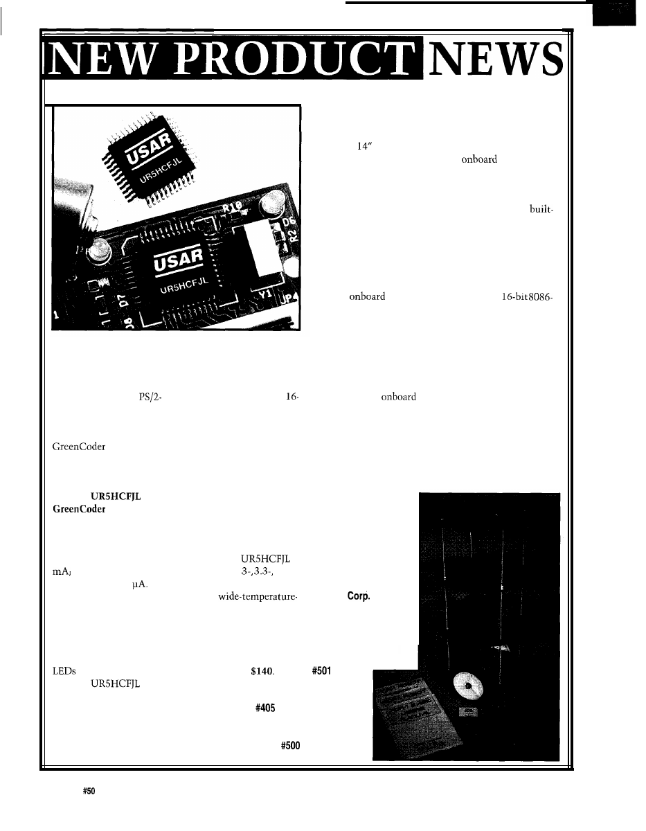
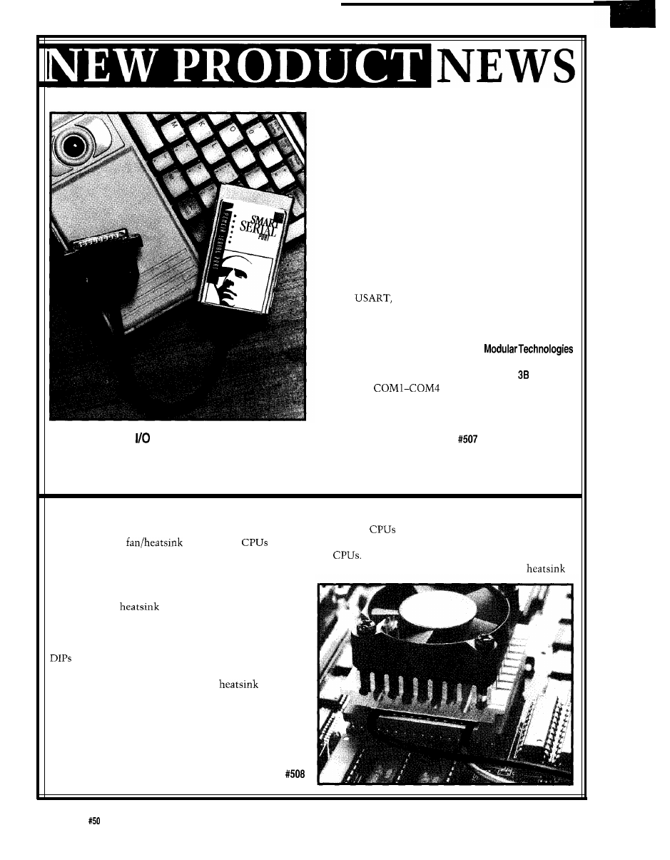
“ZERO POWER”
KEYBOARD
ENCODER
USAR Systems has
announced the first
compatible keyboard
encoder which consumes
hardly any power. The
IC extends
system battery life, has a
small form factor, and is
easy to integrate.
The
regulates
power consumption
based on the keyboard’s
activity. Active, the
keyboard uses only 2
inactive, it con-
sumes less than 2
To
further reduce keyboard
power consumption, the
encoder provides an in-
novative LED dimming
feature-when the key-
board is not in use, the
gradually fade.
The
offers these low-power
advantages without com-
promising functionality
or adding to the complex-
ity of the system. The IC,
which requires no software
drivers or BIOS modifica-
tions, comes equipped with
a full range of technical
features. These include a
bit timer that can be used
for overall system power
management activities such
as CPU wake-up and periph-
eral shutdown, a watchdog
and oscillator monitor cir-
cuit for high-reliability
applications, and a port for
an additional input device.
Ready to connect to
Fujitsu’s FKB Series and
other laptop or palmtop
keyboards, the
is available for
and
5-V systems in DIP, PLCC,
QFP, and
range packages for $3.45 in
quantity. Evaluation kits,
with the IC, sample key-
board, evaluation board,
connectors, and cables, are
also available for
USAR Systems, Inc.
568 Broadway, Ste.
New York, NY 10012
(212) 226-2042
Fax: (212) 226-3215
ROBOT KIT
Aclypse Corp. is shipping the ADR-1 Robot Kit for
the hobbyist and educational markets. The ADR-1 is 27”
tall with a
diameter and weighs approximately 16
lbs. The complete robot kit has an
computer
system that features voice recognition, English speech
output, power motor drive, and a battery with a monitor-
ing and recharging system.
The robot has its own operating system and a
in BASIC programming language for robot instruction.
The system can be programmed by connecting to almost
any computer or terminal through a serial cable. Program
and data files can be sent back and forth between the
robot and a personal computer at speeds up to 19,200
bps.
The
computer is powered by a
compatible CPU operating at 10 MHz with 256 KB of
RAM (expandable) and 128 KB of ROM. A lithium
battery enables data to be retained if power is lost. Two
I/O ports have a total of 12 digital inputs and outputs.
Expansion cards can be connected to add memory,
sensors, motors, and other new devices.
The robot is powered by a 12-V, 6-A battery pack
and contains an
power and recharge module.
The unit features 6” diameter wheels and can move
forward or backward at a speed of up to 8 inches per
second.
No electronics or advanced computer experience is
required to assemble and use the ADR- 1. No special
tools are required and assembly normally takes from 2 to
6 hours. The ease of
assembly makes the
kit ideal for class-
room and lab envi-
ronments.
The ADR- 1
Robot Kit sells for
$499.
Aclypse
Rt. 2 Box 213H
Worthington, IN 47471
(812) 875-2852
BBS: (812) 875-2836
8
Issue
September 1994
The Computer Applications Journal
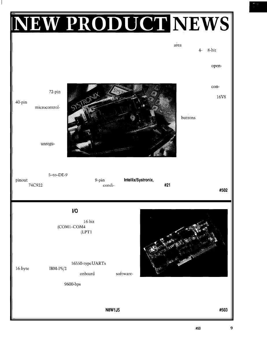
UNIVERSAL DEVELOPMENT BOARD
is ready to be read. A patch
is provided to map the
Intellix/Systronix has released a development board
keypad. The LCD interface accepts most or
that supports all Dallas Semiconductor 805 1 -compatible
parallel LCD displays.
microcontrollers. The DPB2 is a complete, single-board
An 8-bit A/D converter with an adjustable 2.5-5.0-V
computer with LCD and keypad interfaces, serial I/O,
reference voltage is included. Four high-current,
relay-driver outputs, analog-to-digital conversion, rugged
collector relay drivers with snubbing diodes can directly
voltage regulator, and a generous prototyping area.
drive relays, stepping motors, and alarms.
The DPB2 is a 100
Serial loading and
mm x 60 mm (4” x 6.4”)
system reset are
card that contains
trolled by a TL7705
SIMM, 40-pin SIMM, and
monitor chip and a
DIP sockets for
programmable logic
the Dallas
device. Loading can be
lers. Crystal, serial I/O,
initiated by on-card push
and other ports are
or the DTR line
common to all processor
of the RS-232 serial port.
sockets. Processor I/O
Serial loader software is
pins are brought out to
included.
labeled headers. The
The DPB2 is
board accepts
assembled and tested in a
lated 6-13 VDC or can be
variety of configurations,
powered directly with
and is available starting
regulated 5 VDC.
at $199. A bare board
A bidirectional RS-232 serial I/O and RS-232
with documentation is available for $49. Software tools
unidirectional printer output are brought out to 2 x 5
are also available.
headers, and a 2 x
adapter is included. The
is consistent with a standard PC/AT
serial
Inc.
port. A
4 x 4 keypad encoder/debouncer
555
South 300 East, Ste.
l
Salt Lake City, UT 84111
tions the keypad and interrupts the processor when a key
(801) 534-l 017
l
Fax: (801) 534-l 019
SOFTWARE CONTROLLER CARD
Axxon has designed a new peripheral for IBM PC and compat-
ible computers called SOFT I/O. This
product offers four
high-speed serial ports
using the 16550 UART)
plus two bidirectional parallel ports
and LPT2).
The SOFT I/O has been engineered to be completely free of
jumpers for configuring all of the hardware ports. With software,
the user is able to change the address, disable any of the serial and
parallel ports, and select from interrupts 3, 4, 5, 7, 9, 10, 11, 12,
and 15 for any port. The hardware is completely compatible at the
register level with high-speed,
with internal
buffer and
printer port specifications.
Also included is support for an
BIOS using
updated flash memory for future expansion. The high-speed serial
ports are ideal for use with
or faster external modems. The bidirectional ports support scanners and aid in
fast data transfer for laser printers or external printer port-driven tape drives.
The SOFT I/O sells for $299 (CDN dollars) and includes a five-year warranty.
Axxon Computer Corp.
3979 Tecumseh Rd. East
l
Windsor, Ontario
l
Canada
l
(519) 974-0163
l
Fax: (519) 974-0165
The Computer Applications Journal
Issue
September 1994
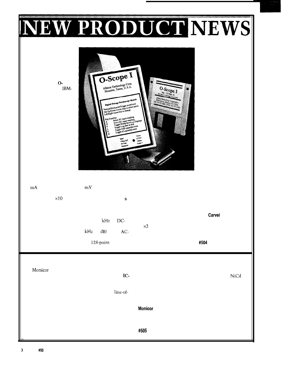
DIGITAL STORAGE
SCOPE MODULE
A low-cost, digital
storage oscilloscope
module has been an-
nounced by Allison
Technology. The
Scope I connects to
PC/AT-compatible
computers via the PC’s
printer port and converts
the computer into a
digital storage oscillo-
scope capable of captur-
ing and displaying DC,
audio, and low-end
ultrasonic frequency
input signals. It can be
used for power supplies,
audio equipment,
automotive, and general
analog design and repair.
O-Scope I is small,
light weight, and por-
table. It draws less than
40
of current from a
12-VDC source. It uses
standard xl and
oscilloscope probes and
works with both desktop
and laptop computers.
Trace sweeps can be
frozen on screen, saved
to disk to be used with
other programs, or
output to a printer via
the DOS print-screen
function. Vertical ranges of
50
to 10 V per division
are provided. Sweep rates of
500 us (xl mode) to 100
per division are available
from most AT compatibles.
The analog frequency range
is DC to 22
for
coupled input and 1 Hz to
22
(-3
for the
coupled input option.
A
Fourier
spectrum analyzer mode
provides frequency spec-
trum information from DC
to one-half of the current
sample rate. There are 50
samples per division in the
xl sweep mode. Two forms
of sweep expansion are
provided. Expansion modes
of
and x5 spread out the
sweep by separating
samples. Special DSP
expansion modes are
available from x2 to xl 6
which will expand the
sweep by adding calcu-
lated samples based on
the frequency content of
the captured sweep
signal. In addition to the
sweep, O-Scope I
provides voltage,
frequency, and period
calculations. Voltage
measurements include
peak-to-peak, average,
peak, minimum, and
RMS. If more than one
cycle exists in the sweep,
a frequency and period
are calculated. If less
than one cycle exists, a
pulse period is calculated
instead.
O-Scope I sells for
$169.95 including an AC
adapter and cable. A kit
version, which is pro-
vided without the
shielded case, is also
available for
$119.95.
Allison Technology Corp.
8343
Houston, TX 77036
(713) 777-0401
Fax: (713) 777-4746
RADIO MODEM
has announced a low-cost radio modem
which eliminates the need for an RS-232 cable. The
15 Radio Modems
contain a UHF radio transceiver that
supports 2400 and 4800 bps. A sensitive receiver,
powerful transmitter, and fast protocol support
sight distances up to one mile. Greater distances are
possible with optional gain antennas.
Each radio has an intelligent RS-232 communica-
tions port that can be completely configured for any
terminal. Data rates are up to 19,200 bps.
The point-to-point radios are ready to use and are
completely self-contained in a Lexan housing. They
come complete with an antenna, a rechargeable
battery, and a battery charger. Each radio weighs only 22
oz. The dimensions are 9” x 3” x 1.7”.
The IC- 15 Radio Modem sells for $950 each (2400
bps) and $1400 each (4800 bps).
Electronics Corp.
2964 NW 60th St.
l
Ft. Lauderdale, FL 33309
(305) 979-1907
l
Fax: (305) 979-2611
Issue
September 1994
The Computer Applications Journal
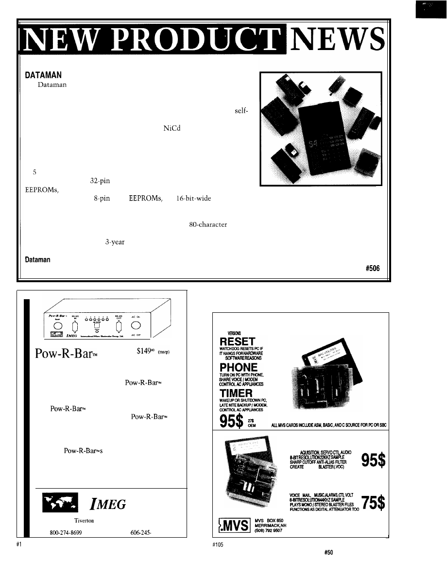
S4 PROGRAMMER
has announced improvements to their popular S4
hand-held
EPROM Programmer/Emulator.
The S4 now comes standard with 5 12 KB
(4 Mbit) of RAM.
Approximately 7” x 4” x 2” and weighing just over a pound, S4 is
powered and completely portable, making it useful for field service work.
S4 can operate for several days on its internal
battery or be used as a
conventional desktop programmer, controlled remotely by any computer
with an RS-232 port. Besides functioning as a programmer, S4 can also be
a ROM emulator. Included with each unit is an emulation cable that
plugs directly into the target system in place of any EPROM or ROM up
to 12 KB x 8 bits.
Equipped with a
ZIF socket, the S4 supports EPROMs,
and flash memory up to 8 Mbits. It can also program PIC and
8751 microcontrollers,
serial
and
devices using optional adapter modules. Additional
socket converters are also available for a variety of surface-mount packages. The comprehensive device library is
regularly updated to support new devices. Upgrades can be downloaded free of charge from Dataman’s 24-hour
bulletin board. Other features include a high-contrast,
LCD with a wide viewing angle, 45 color-coded
rubber keys (nonbreakable), and a high-impact, molded plastic case which fits comfortably in the palm of your hand.
S4 is covered by a full
warranty and costs $795.
Programmers, Inc.
22 Lake Beauty Dr., Ste. 101
l
Orlando, FL 32806
l
(407) 649-3335
l
Fax: (407) 649-3310
is an
intelligent, programmable, six outlet power
strip which connects
to a computer’s serial port and
operates via RS-232 protocol.
is the
perfect solution for controlling multiple AC outlets.
With
connected to a computer, each of
the six AC outlets on the back of
can
be turned on/off from the computer, by typing in a
simple command or through custom programming.
Up to 26
can be daisy chained to-
gether providing up to 156 outlets individually con-
trollable from a single computer. With this system,
an entire building can be automated.
International
Micro Electronics
G r o u p ,
L t d .
155 W.
Lexington, Kentucky 40503
P.O. Box 25007 Lexington, Kentucky 40524
606-271-0017 Fax:
1798
REMOTE POWER CARD!
3
OR
UNE,
8 CHAN ADC
DATA
RATE
STEREO
FILES
2 CHAN DAC
RATE
5 YEAR LIMITED WARRANTY
F R E E S H I P P I N G I N U S A
The Computer Applications Journal
Issue
September 1994
11
04
system equipped with a
Type II slot. The card offers
asynchronous compatibility
with all DOS- and Win-
dows-based software and
connects to all standard
serial peripherals. It also
features synchronous
operation for high-speed
data transfers with main-
frames.
The serial I/O card
includes an internally
buffered 16550 UART and
an 8530
a combina-
tion that provides the
flexibility of either asyn-
chronous or synchronous
communication. It also
provides the flexibility of
configuring the asynchro-
nous port as
while the synchronous port
is fully programmable. Its
software eliminates the
standby mode, which is
automatically entered
when no activity has
been detected for a period
of time, power is re-
moved from most of the
card’s internal circuitry.
In the sleep mode, the
host computer essen-
tially turns off the card’s
power. This mode is
entered and exited under
the control of the host
computer using the
PCMCIA interface.
The Serial I/O card
sells for $145 in quantity.
Smart
45531 Northport Loop
West, Bldg.
Fremont, CA 94538
(510) 623-l 231
Fax: (510) 623-l 434
PCMCIA SERIAL
developed a PCMCIA serial
need to set any jumpers.
CARD
I/O
card for use in any
The card’s power-down
Smart Modular
Technologies Inc. has
subnotebook, PDA, palmtop
mode conserves power and
computer, or other host
extends battery life. In the
CPU COOLING DEVICE
The Turbo Chip Cooler (TCC) from Discovery Data Systems keeps
almost 60°F cooler at room tempera-
ture than typical
chip coolers.
will last longer and operate with wider timing margins for all
computers. The device is especially effective with higher speed
The solid-state refrigerator used in the TCC literally extracts heat from chips without the need for the
gels, special clips, or clamps required by other types of
chip coolers. In most cases, when combined with a
typical fan and
combination, it maintains the
CPU at or below room temperature.
The TCC can be used with any CPU, including 286,
386,486, Pentium, 680x0, and other processors (even
and socketed types). Special heat-conductive
mounting pads, provided with the TCC, allow it to
conveniently mount with any chip or
combina-
tion. A single model fits all devices and can be installed
without tools.
The Turbo Chip Cooler sells for $34.95.
Discovery Data Systems
12572 Westmont Dr.
l
Moorpark, CA 93021
(805) 529-1325
l
Fax: (805) 523-8153
12
Issue
September 1994
The Computer Applications Journal
‘URES
Time to Meet Big Brother:
Exploring the
DRAM on an 8031:
Not as Hard as
You’d Think
Motorola’s 68322
Processor: Redefining the
Low-end Laser Market
Preventing the Ultimate
Blow: A Portable
Checking Unit for 8751s
Understanding PC Buses
Time to Meet
Big Brother:
Exploring the
Dana Romero
any articles have
written about
applications of the
family of
micros, a family long established in
the field of embedded control. As an
alternative, I would like to discuss
Motorola’s approach to microcontrol-
ler design with the
their
“next step” after the
Having worked with the
in the past and being famil-
iar with its architecture and command
set, when I read that Motorola was
offering a development kit for the
16, I bought one immediately.
The package turned out to be well
worth the money-loads of software,
programming examples, documenta-
tion, and even an introductory book on
digital signal processing. In fact, the
board and software are oriented toward
prototyping A/D and D/A conversions
for use in DSP. A much simplified
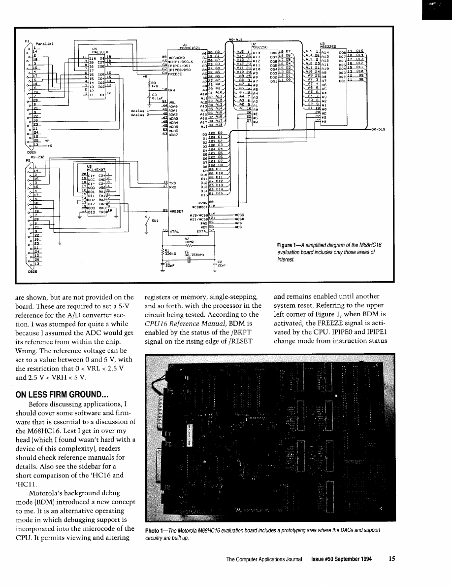
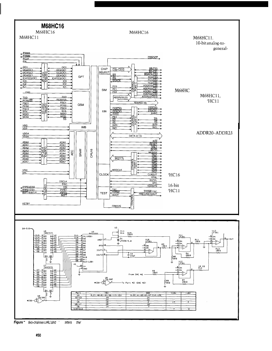
diagram of the board is shown in Fig-
ure 1. Note that all the signals shown
are also sent to 20-pin connectors,
which have through holes for extend-
ing them to a wire-wrap area (Photo I).
I’ve left out many signals that this new
micro provides, but aren’t used in this
basic introduction.
Shown in the photo is a socket for
a Burr-Brown serial D/A converter,
which I didn’t have access to and
wouldn’t have suited my purposes
anyway. Both parallel and serial ports
are provided. The parallel port,
is
the primary communication path with
a PC via its printer output; the serial
port,
is secondary and is intended
for a dumb terminal or another PC
with communications software. Last,
note that the components R3 and C3
14
issue
September 1994
The Computer Applications Journal
l--The
subroutine calculates
x
Enter
in location ARG
and the
is returned in register.
EQU
EQU
CF4
ARG
EQU
ARG4
EQU
ARG8
ORG
DC.W
$9151
DC.W
$0300
ORG
$0200
***** Initialization Routines
INCLUDE
INCLUDE
INCLUDE
INCLUDE
INCLUDE
one over PI squared
over 24
over 720
over 40320
reset vectors
interrupt vectors
set
ZK=O
set sys clock at 16.78 MHz
disable COP
initialize and turn on SRAM
set stack
***** Set up Port as an output *****
LDAB
STAB
PFPAR
LDAA
STAA
DDRF
STAB
PORTFO
Compute powers of x
LDZ
START: LDD
STAB
TDE
EMULS
ADCE
STE
LDD
EMULS
ADCE
TED
EMULS
ADCE
STE
LDD
TDE
EMULS
ADCE
STE
TED
EMULS
ADCE
STE
PORTFO
ARG,Z
of x
port as general I/O
;now set port as
initial value
to bank zero
odd value of
multiply E*
into E
square of x
sixth power of x
fourth power of x
eighth power of x
an output port
to zero
ARG to port
n
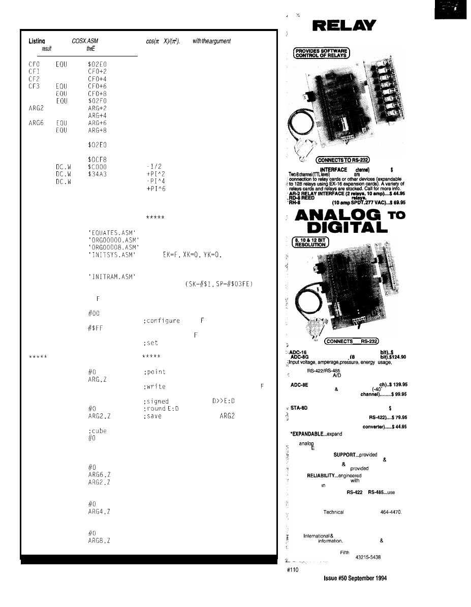
INTERFACE
AR-16 RELAY
(16
. . . . . . . . . . . .
89.95
outputs provided
for
RELAY CARD (8
10 VA) . . . . . . $49.95
RELAY CARD
TO
A/D CONVERTER* (16 channel/8
99.95
A/D CONVERTER* channel/IO
joysticks and a wide variety of other types of analog
signals.
available (lengths to 4,000’).
Call for info on other
configurations and 12 bit
converters (terminal block and cable sold separately).
TEMPERATURE INTERFACE’ (8
Includes term. block 8 temp. sensors
to 146’ F).
STA-8 DIGITAL INTERFACE* (8
Input on/off status of relays, switches, HVAC equipment.
. security devices, smoke detectors, and other devices.
TOUCH TONE INTERFACE* . . . . . . . . . . . . . . . .
134.99
Allows callers to select control functions from any phone.
PS-4 PORT SELECTOR (4 channels
Converts an RS-232 port into 4 selectable W-422 ports.
CO-485 (RS-232 to RS-42WRS-485
your interface to control and
monitor up to 512 relays, up to 576 digital inputs, up to
128
the PS-4,
inputs or up to 128 temperature inputs using
X-16, ST-32 &AD-16 expansion cards.
FULL TECHNICAL
over the
telephone by our staff Technical reference disk
including test software programming examples in
Basic. C and assembly are
with each order.
HIGH
for continuous 24
hour industrial applications
10 years of proven
performance the energy management field.
CONNECTS TO RS-232,
or
with
IBM and compatibles, Mac and most computers All
standard baud rates and protocols (50 to 19,200 baud).
Use our 800 number to order FREE INFORMATION
PACKET.
Information (614)
24
HOUR ORDER LINE (800) 842-7714
Visa-Mastercard-American Express-COD
Domestic FAX (614) 464-9656
Use for
technical support orders
ELECTRONIC ENERGY CONTROL, INC.
360 South
Street, Suite 604
Columbus. Ohio
(continued)
The Computer Applications Journal
1 7
Real-time Emulator
Introducing
and
real-time in-circuit
emulators for the
family microcontrollers: affordable,
feature-filled development systems from
for
“AND/OR”
Breakpoints
n
Trigger Outputs on any Address Range
n
12 External Logic Probes
Internal Clock from
frequencies or External Clock
Single
Multiple
To Cursor,
Step over Call, Return
Caller, etc.
. On-line Assembler
for patching
i n s t r u c t i o n
n
Support
and
with
Optional Probe Cards
n
Easy-to-use Windowed Software
n
Comes Complete with
Macro
Assembler, Emulation Software, Power
Adapter, Parallel Adapter Cable and
User’s Guide
n
Money Back Guarantee
n
Made in the U.S.A.
family emulation up to 20 MHz. It offers the
real-time feature5 Of
RICE16 without the real-time trace capture.
Gang Programmers
Advanced Transdata Corp. also
QUALITY
gang programmers for the different PIC microcontrollers.
Stand-alone COPY mode from a master device
n
PC-hosted mode
for single unit programming
n
High throughput
n
Checksum verification
on master device
n
Code protection
n
Verify at
and
Each
program cycle includes blank check, program and verify eight devices
Price5
start at
18
Issue
September
1994
The Computer Applications Journal
for
family
Throughput:
4
(0
devices)
10
PGM47: for
10
15
for
13
Call (214) 980-2960 today for our new catalog.
Advanced
Corporation
Tel
14330 Midway Road, Suite 120, Dallas, Texas 75244
Fax (214)
See us
at
Embedded Systems West booth
For this reason the stored arguments,
need to be divided by
two to be in the proper format for the
MAC command. The four
LSRW
instruc-
tions just before the MAC section
handle this.
Before running this program from
within EVB16, be sure to first set the
data window (F3) with the command
MD
F3 0 2 E 0
to display the coefficients
CFO-CF4 andthevalues ARG-ARG8.
(You can watch the
being
changed if you trace through the pro-
gram with the Tn command, where n
is the number of steps to trace.) To
watch the timing on a scope, preload
ARG with an odd value using DMM. W
0 2 F 0 from within the (debug] win-
dow. The odd value sets Port F’s bit
zero to one for the duration of the
loop. Since port F has been configured
as an output port, the signal MODCLK
is now redefined as FO. Your scope
probe on this line will show the time
that it remains positive.
I measured 100 for one loop.
Although that seems slow, there are a
lot of
and
calculations going
on. Interestingly, eliminating the
eighth-power term of the approxima-
tion only reduces the calculation time
to 90 us. Timing would be a concern if
one wanted to output a waveform.
D/A EXPERIMENTS
One of the first things that I
wanted to do with the
board was to experiment in generating
audio waveforms that would be diffi-
cult or impossible to produce with
analog circuitry alone. My ultimate
goal was to produce unique tones.
Using the prototyping area on the
board, I added two
whose
outputs are then sent to a summing
junction as shown in Figure 2.
I summed the two DAC outputs
so that one could provide a fundamen-
tal or low-frequency tone while the
other provided a harmonic or
high-frequency tone. Alterna-
tively, one DAC might help generate
an envelope of sorts for the other’s
tone, and so on. (Note that, just be-
cause the circuit uses DAC 1222 con-
verters, you’re not restricted to the
slower response of
resolution.
Instead, through software, a
Listing l-continued
LSRW
LSRW
LSRW
LSRW
Multiply and accumulate
ORP
CLRD
TDMSK
LDE
TEM
LDX
LDY
LDHI
LOOP:
MAC
BNE
TMER
STE
RTS
CLRD
STAB
LDAB
DELAY: DECB
BNE
JMP
BDM:
BGND
format for MAC command
saturation mode in MAC reg
term is one over
LOOP
PORTFO
DELAY
START
last coefficient?
return with rounded result in E
remove this to measure timing
all bits set to zero
negative state for scope timing
output
port can be used for
or
conversions.)
I wired both
for bipolar,
rather than unipolar, operation.
I
adapted the circuitry, not from Na-
tional Semiconductor, the manufac-
turer, but from Analog Devices’ speci-
fication for the
(As far as I
can tell, the chips are functionally the
same.) The outputs for given input
codes are listed in Table
1.
Note that
V
as referred to in the table is the
voltage that will appear at the output
of either
or
op-amp U13 will
produce the negative sum of these
voltages at its output. Also,
is set
by voltage reference
and potenti-
ometer R14 and goes to
of both
With this hardware in place, the
real complexity comes in the software.
The fact that decoded chip selects
come directly from the microcontrol-
ler means more work in software. A
program that produces a basic audio
waveform is S
P I K E A SM
(see Listing
2). This program shows how to set
up the chip selects, output to the
The BCC52 controllercontinuesto be
Micromint's best selling single-board com-
puter. Its cost-effective architecture needs
onlyapowersupplyandterminalto become
a complete development system or
board solution in an end-use system. The
BCC52 is programmable in BASIC-52, (a
full floating point interpreted
BASIC), or
assembly language.
The BCC52 contains five RAM/ROM
sockets, an “intelligent”
EPROM
programmer, three parallel ports, an
auto-baud rate detectserialconsole
printer
much more.
PROCESSOR
CMOS processor w/BASIC-52
Console RS232
detect
RS-232
parallel ports
EXPANDABLE1
12
expansion boards
B C C 5 2
Controller board
BASIC-52 and SK RAM
$189.00
Low-power CMOS
of the
$ 1 9 9 . 0 0
temperature
$ 2 9 4 . 0 0
Low-power CMOS, expanded
RAM
$ 2 5 9 . 0 0
CALL FOR OEM PRICING
MICROMINT, INC.
Canada:
Inquires
Bar Code Sensor
Battery Controllers
Clock/Calendars
Digital Power Drivers
DTMF Phone Interfaces
Firmware Furnace Widgets
HCS-II Hard-to-find Parts
Bus
Photodiodes
Data Link Parts
Remote Control
Laser Diode Controllers
Linear Hall Effect Sensor
Crosspoints
Power Op Amp
Remote Temperature Sensor
Stepper Motor Drivers
Watchdogs Power Monitors
8051 Information
and more!
Use a soldering iron? Get the parts!
UPS:
day $6 5019.00 to 48 US states, COD add $4.50. PO Boxes and
addresses. $6 for USPS
Check, MO, or COD only; no credit cards,
no open
NC residents add 6% sales tax.
discounts start at five parts.
Data sheets Included with all parts.
Call/write/FAX for seriously tempting catalog...
Pure
Your unusual part5 source
13109
Old
Raleigh NC 27613-7421
FAX/voice
The Computer Applications Journal
Issue
September 1994
19
Meet the
The
is Motorola’s 16-bit step after the
line of microcontrollers. Additional features
make it more suitable for digital signal processing. The
architecture is based on modules similar-but
not identical-to those used in the
These
modules include a CPU core, RAM,
digital converter (ADC),
purpose timer (GPT), queued serial
module (QSM), system integration
module (SIM), clock control, and
port or chip selects. All these
modules are running on one IC at
16.77 MHz.
Although the basic modules of
the
16 are named differ-
ently than in the
most
of the features of the
are
present in the ‘HC16. Of course,
the data path is 16 bits wide, and it
has 1 MB of data space and 1 MB of
code space. Although the documen-
tation implies that the address bus
is 24 bits wide,
follow the output of ADDR19.
According to the Technical
Summary, these are brought out to
pins only for test purposes. This
summary also claims that the
‘HC16 is upwardly code compatible
with the ‘HC 11. However, the
has no instructions to
increment or decrement any of the
registers directly as the
does with the INX and INY
instructions. The only instructions
that comes close are A I X and A I Y:
add immediate to X or Y. The
Z
--
H
some
on outputs can be used to generate tones under processor control.
20
Issue
September 1994
The Computer Applications Journal
processor would be more accurately said to be “upwardly register compat-
ible.”
The
Reference Manual
devotes a whole appendix to the
comparison of the two command sets. Looking at the registers found on the
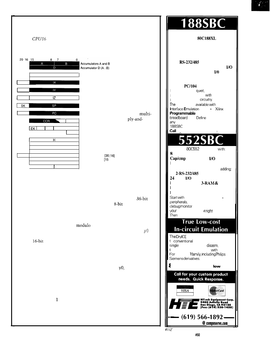
‘HC16, you’ll see that the shaded registers in the diagram are also found in
the ‘HC 11, but
that the
condition code
register is only
E
Accumulator E
partially
XK
Index register X
shaded. This
YK
Index register Y
partial shading
is because the
ZK
Index register Z
‘HC16 adds
.
Stack pointer
three new
flags, devoted
P K
Program counter
to
the
PK Condition code register
accumulate
XK YK ZK Addressextension (K) register
SK Stack extension register
(
MAC
) register,
and a field of
MAC multiplier register
three bits to
35
I
MAC multiplicand register
16
mask eight
interrupts. The
AM (MSB)
MAC accumulator
AM (SLB)
MAC accumulator
: 0]
“K” extension
registers are
[ XMSK
YMSK MAC mask register
four bits each
and concat-
enate with their corresponding 16-bit registers to form 20-bit addresses,
with the exception of the EK register. The EK register concatenates with a
word following an opcode in the extended addressing mode.
A significant conceptual difference between the ‘HC 16 and the ‘HC 11
comes with the addition of the MAC section, which consists of a
accumulator (AM), multiplier registers (H and I), and
mask registers
(XMSK and YMSK). This section was specifically designed for DSP calcula-
tions. XMSK and YMSK are used for modulo addressing. Readers should
study these for their own applications; but for now, it is sufficient to say
that setting both to zero disables
addressing.
With this in mind, a single MAC instruction of the form MAC x0,
performs the following sequence:
1. A
signed fraction in the H register is multiplied by the same in
the
I
register; the product is shifted left once to align the decimal and then
placed in the 32-bit register, E:D. DO is set to zero.
2. The aligned product is added to the current contents of AM, and
flags in the CCR are set accordingly.
3. The X and Y registers are incremented by x0 and
respectively.
4. Contents in H are saved in the Z index register.
5. The word pointed to by XK:IX is loaded into H and the word pointed
to by YK:IY is loaded into I.
Before using the MAC command, place values into H and I with LDH I,
which loads H with the word pointed to by XK:IX and I with that pointed to
by YK:IY. See Listing for an example.
Power on the
4 layer board
I S
provided by a switcher
watchdog and
power fail interrupt
188SBC
IS
Extended
of I/O a
Field
Gate Array a n d a
area.
and design nearly
extra Interface you need we’ll help!
prices start at $299.
right now for a brochure!
The
IS
an 8051
ch. 10 bit A/D
2 PWM outputs
registers 16
lines
US-232 port
Watchdog
We’ve made the
552SBC
by
multi-drop ports
more
Real-time Clock
EEPROM
l-ROM
Battery Backup Power Regulation
Power Fail Int.
Expansion Bus
the Development Board all the
power supply, manual and a
for only $349. Download
code and debug
on this SBC.
use OEM boards from $149.
Plus
IS
a low-cost alternative
o
ICE products. Load,
step, Interrogate,
execute
o breakpoint. Only $448
a pod.
the 805
and
Call for brochure!
3031 SBC
as
as $49
S i n c e 1 9 8 3
70662.1241
Use Turbo or MS ‘C
Intel
Two 1 meg Flash/ ROM sockets
Four battery backed, 1 meg RAM
16 channel, 12 or 16 bit A/D
8 channel, 12 bit D/A
2
serial, 1 parallel
24 bits of opto rack compatible
20 bits of digital
Real-time clock
Interrupt and DMA controller
8 bit,
expansion ISA bus
The Computer Applications Journal
Issue
September 1994
21
Listing
program produces an audio waveform by shifting the register.
INCLUDE
of
for common regs
INCLUDE
reset vector
INCLUDE
interrupt vectors
ORG
$0200
prog after interrupt vectors
*****
Initialization Routines
INCLUDE
INCLUDE
Start of main program
EK=F, XK=O,
ZK=O
clock at
disable COP
and turn on SRAM
stack
LDD
STD
LDD
STD
LDD
STD
LDD
STD
STD
CSBAR8
CSOR8
set
as
block size =
CS6 active when address =
block size =
CS8 active when address =
chip selects are asynchronous,
write only with data strobe,
in user space
Set DAC for offset voltage
LDX
LDAB
TBXK
LDAA
LDAB
STD
Increment and send word
START: LDAA
LDAB
TBXK
LDAB
STD
ASLD
CMPA
BMI
OUT1
CLRB
LDAA
STD
$0000,X
ASRD
BCC
OUT2
JMP
START
***** Exceptions/Interrupts
BDM:
BGND
for proper chip select
gives zero volts
gives DC offset
value:
or
to DAC
with D= 0004
by two
when A>8
A B
by two
vectors point here
and put the user in bckgrnd mode
and use the D register for
moved from a sine wave-change a
shifts.
few parameters and the results look
An oscilloscope on the output of
quite different. Specifically, DAC
U13 shows what first appears to be a
has been held at a constant offset. At
rectified sine wave (Figure 3). But a
the next level, we can vary this
close examination of the program and
ing to external input such as the A/D
the waveform show that it is far re-
section or an interrupt, for example.
22
Issue
September1994
The Computer Applications Journal
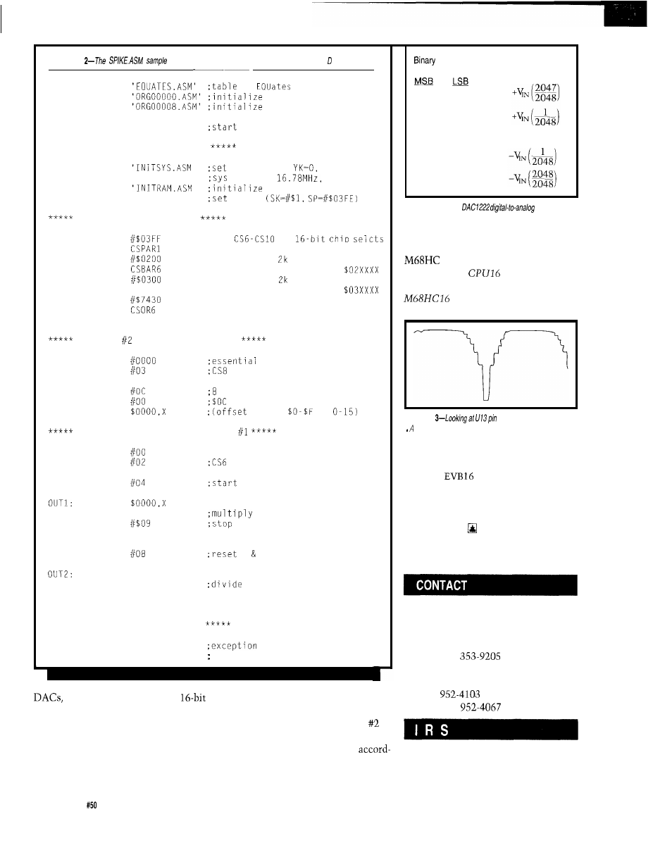
into DAC
Analog Output
1111
1111 1111
1000
00000001
1000
00000000
o v
0111
1111 1111
0000
00000000
Table l--The
converter
produces a bipolar output referenced to V,,
From here, it’s up to your imagina-
tion. If you plan to work with the
16, you really should have the
following: the
Reference
Manual (software descriptions), the
User’s Manual [for voltage
Figure
6 when running SPIKE
SM produces something like a rectified sine wave.
and timing specifications), and the
MASM16 assembler from Motorola.
Also, the
debugger and PAL
firmware from P&E Microsystems
work quite well with MASM16 and
greatly speed learning the ins and outs
of this device.
Dana Romero holds a B.S. in Math-
ematics from the University of Utah.
P&E Microsystems
P.O. Box 2044,
Woburn, MA 01888
(617) 944-7585
Fax: (617)
Motorola
(602)
Fax: (602)
401
Very Useful
402 Moderately Useful
403 Not Useful
DRAM on
an 8031:
It’s Not as
Hard as
You’d Think
Hugo Cheung
any microproces-
sor applications such
as data logging, printer
buffering, and serial and
parallel data conversion require large
amounts of data memory. Typically,
most applications need a few hundred
kilobytes to a few megabytes. SRAM,
which is expensive and takes up a
large PCB area, does not provide a
practical solution. DRAM, on the
other hand, costs about $30 per
megabyte making it a good candidate
for this kind of application.
However, using DRAM is incon-
venient because of its need to be
refreshed with burst modes or cycle
stealing. Burst refresh requires the
CPU to stop accessing the refreshing
DRAM. Cycle stealing, which I use in
this application, refreshes the DRAM
during the CPU instruction fetch
cycle: Unlike the methods used for the
IBM PC, XT, or AT, these refresh
techniques have no software overhead
and the CPU doesn’t need to halt
while DRAM refreshes.
After looking at the timing for
DRAM, I’ll investigate the timing for
the 8051 (or any 8051 family device).
Specifically, I’ll look at how we can fit
DRAM into an 805 1 application. Since
understanding the detail timing of a
system is critical to implementing
DRAM in an application, I’ll provide a
lot of timing diagrams along with
circuit diagrams.
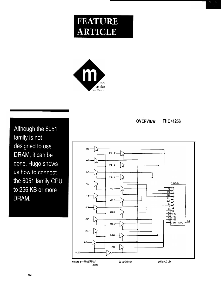
O
F
D
RAM
To implement my data logger, I
decided to use eight 41256 memory
chips. The 41256 is organized as
1 x
D I N D O U T
requires a multiplexer
column or row address
pins. The switching
is controlled by the
signal.
24
issue
September 1994
The Computer Applications Journal
41256.
When
41256
/MUX is high, the
AO-A8
Row Adr
Column Adr
microprocessor’s
P1.l,
\
Row Adr is latched
and P1.2 are
routed to the
S w a p R o w A d r w i t h C o l A d r
41256’s
AO-A8
pins.
\ Col Adr is latched
Figure 2
shows the timing
for
Figure
row and column addresses into DRAM. The
address multiplexing signal
has
between
and
first goes active
256
Kb of RAM and uses separate data
input and output lines. It requires 18
address lines to give it a total of 256K
address locations. The address lines are
multiplexed to nine pins (AO-AS). The
active-low multiplexing control
signals are
(column address
strobe) and
(row address strobe).
All together, the 41256 has a total of
16 pins, including the /WE (active-low
write-enable signal) and two power
pins
V and ground).
When
is asserted, the
when /MUX is low, indicating the
low-order address bits are being
presented to the DRAM. Next, /MUX
goes low and
is asserted to tell
the DRAM that the high-order address
bits are being presented. These three
signals are generated by a PAL
I
will describe the details of the PAL’s
contents later.
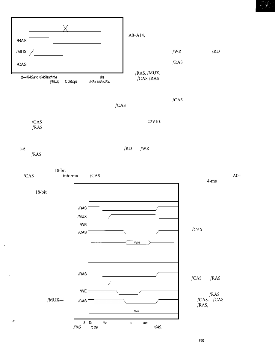
HOW TO READ AND WRITE DRAM
The 805 1 has
and
signals for data memory read and write
DRAM read and write timings. The
DRAM read/write sequence of events
is as follows:
1. Al5
is low (address = OOOOH to
7FFFH) and /MUX is low
2.
is low to write;
is low to
read
3.
goes low to latch the row
address
4. /MUX goes high to switch the
DRAM address bus from the
column to row address
5. /WE goes low to write to DRAM or
it goes high to read from DRAM
6.
goes low to latch the column
address
information on the nine address lines
timing control. /WE, which is the
is latched internally and is used as the
write-enable signal for the DRAM, has
lower 9 bits of the total
address.
to be valid after /MUX and before
When
is asserted, the
become active. Figure 3 shows
tion on the nine address lines
is used as the upper 9 bits of
the complete
address.
DRAM Read Timing
41256
ADDRESS MULTIPLEXING
AO-A8
Row
Adr
Column Adr
X
The 8031 has 64 KB of
\
address space for data
memory and I/O. In my
\
application, 32 KB from
OOOOH to 7FFFH is allocated
for the DRAM. The 256 KB
DRAM requires 18 address
Din
lines. However, the CPU can
only provide 15 address lines
(AO-A14) from the address
DRAM Write Timing
bus. To get the remaining
41256
lines, I used three bits of the
AO-A8
Row
Adr
Column Adr
CPU’s Port 0 to make up a
\
total of 18 address lines for
the DRAM.
/ M U X
\
Figure 1 is a simplified
circuit diagram of the address
multiplexer. When
the control line to the
multiplexer-is low, the
Dout
microprocessor’s AO-A7 and
.O are routed to the AO-A8
address input pins of the
Figure
access DRAM, we have prepare row address, activate
switch column address, set up /WE, and activate
HOW TO REFRESH DRAM
The information contained in the
internal storage cells of dynamic RAM
must be accessed periodically to keep
it valid. Typically, the information in a
DRAM storage cell remains valid for
only a few milliseconds. If the cell is
not refreshed, the data is lost.
When data is read from the 41256,
an entire row of the internal cell is
refreshed in parallel. An entire RAM
chip can be refreshed by accessing
A7 during a
refresh
period. To do this, we need to
have a refresh counter, which
can be implemented in
software or hardware. How-
ever, to avoid the software or
hardware overhead necessary
to implement such a refresh
counter, we can instead use
the
before
IRAS refresh
method.
Most DRAM currently
available on the market has a
built-in refresh counter and
refresh-timing generator. The
internal refresh clocks and
refresh counters can be
initiated by special timing in
the
and
signals.
From Figure 2, we know that
read or write timing normally
requires that
be active
before
If
is active
before
though, the
DRAM internal decoding logic
will trigger the internal
refresh clock and counter.
Consequently, a simple
The Computer Applications Journal
Issue
September 1994
2 5
Machine Cycle 1
Machine Cycle 2
PI
PI
PI
PI
XTAL2
ALE
r
r
Port0
Port2
/MUX
Figure
DRAM is read by the CPU, the
generated by a state
machine and depend on the machine cycle and its state
DRAM refresh circuit can be realized
by carefully arranging the
and
timing.
BUS TIMING IN 8051
Read and write timing for program
and data memory is critical for the
805
1
controller. To accomplish DRAM
refresh by cycle stealing, we have to
understand the timing of the 8051 bus;
otherwise, we cannot determine where
to steal cycles.
Unlike other
the 805 1 is
optimized for control applications. It
has 64 KB of program memory address
space and another 64 KB of data
memory address space. Because the
805 1 doesn’t store program code in
data memory, a program opcode only
has to be retrieved from program
memory. During an opcode fetch, data
memory is not used. We can, therefore,
steal opcode cycles for DRAM refresh.
The 8051 bus timing is divided
into machine cycles. A machine cycle
consists of a sequence of six states,
numbered
Each state time lasts
for two oscillator periods. Thus, a
Everything You Need for Embedded 80x86 Development
Debug code from your existing C/C++ compiler
l
Soft-Scope supports compilers from Microsoft, Borland, Watcom,
and Intel
l
For real- and protected-mode
and 32-bit embedded applications
l
Supports
80x86 family including 80486 and i
l
Available as a DOS .exe or
Embed a DOS or Windows
executable file
l
CSi-Locate supports C/C++ compilers from
Microsoft, Borland and Watcom
l
Creates HEX, binary and absolutely located files
Royalty-free monitor
with complete source code
l
Include the monitor in your application for easy in-the-field maintenance
l
Configuration utility makes monitor quick to install
Debug real-time applications
l
Supports Intel’s
C
and Industrial Programming’s
Since 1983
l
We introduced the original source-level 8086 debugger in 1983
l
We are experts in 32-bit protected mode embedded development
Bringing Insight into 80x86 Family Embedded-System Development
530 S.
l
P.O. Box 9666
l
Moscow, ID 83843 USA
l
(208)
l
FAX (208) 882-9774
Issue
September 1994
The
Computer Applications Journal

machine cycle takes 12 oscillator
periods or
1
if the oscillator fre-
quency is 12 MHz.
Figure 4 illustrates the
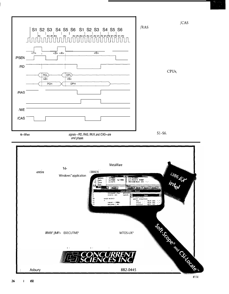
data-memory read timing. XTAL2
represents the oscillator clock timing.
ALE (address latch enable) outputs a
pulse to grab a low byte of the address
during access to external memory. At
point
ALE latches the CPU
program counter low (PCL) byte. This
combines with the program counter
high (PCH) byte at
to provide a
bit program memory address. EPROM
data (opcodes) will be sampled at of
S4
At
ALE latches the DPL
(data pointer low) byte value or register
bits for other instructions. Combining
with the DPH (data pointer high) byte
data at
a 16-bit data memory
address is ready. The external data
memory (
DR
AM) will be sampled at
of S3
is active for the
data read control.
Figure 5 shows
memory write timing. When
is
active, data to be stored in memory is
present on Port 0.
Machine Cycle 1
Machine Cycle 2
P2
P2 PI P2
P2 PI P2
P2
P2
P2
P2 P2 P2
P2
XTAL2
ALE
r
r
Port0
Data
P C H
DPH
/MUX
Figure
data memory write
is similar to the read cycle, but
DRAM/WE signal is asserted to indicate
data is being written to
The Computer Applications Journal
Issue
September 1994
27
DRAM READ/WRITE TIMING
AND EQUATIONS
In order to make the PAL equa-
tions easy to match up with the timing
shown in Figures 4 and 5, I define the
bus states as
for of
S12 for
P2 of
and so forth through S62 (see
Table 1). I’ll discuss how to generate
1
through S62 later. The PAL
equations are shown in Listing 1.
Listing l--The
source listing describes
equations for a
which is used to
a
Gray-code state machine that is decoded to generate control signals for DRAM access circuit.
TITLE DRAM8051
PATTERN DRAM REFRASH FOR 8051
REVISION 0.1
AUTHOR HUGO CHEUNG
COMPANY
DATE l-31-93
First I define a general-purpose
DRAM chip select signal for use inside
the PAL as follows:
CSDRAM =
l
*
THIS PAL GENERATE CAS RAS WE SIGNAL FOR
; DRAM 41256 READ WRITE ACCESS AND ALSO
CAS BEFORE RAS REFRESH SIGNALS FOR 8051
;
0 1 1 1 1 1 1
During a data memory access,
is the first signal we need to
activate and is programmed to be
active during
S12, S21, S22, S31,
and S32 of machine cycle 2. The
equation for
is:
CHIP DRAM8051
2
3
4
5
6
7
8
9
11 12
PALCK ALE RD WR PSEN Al5 Al4 RESET NC NC
NC GND
14 15 16 17
18 19 20
21 22
23 24
NC
PO P3
MUX RAS CAS
WE
NC VCC
= CSDRAM *
+ S12 + S21 +
GLOBAL
S22 S31 S32) + REFRAS
where REFRAS is the
refresh
condition (to be discussed later). In
Figure 6,
is connected to eight
41256 chips.
/MUX is changed one clock cycle
after
If a 12-MHz oscillator is
used, this clock cycle is 83 ns long and
is known as the
address hold
time
Normally, DRAM requires
a minimum
of
ns, so we
are well within
From this
analysis, we can program /MUX to
be active during S12,
S22,
and S32 of machine cycle 2. The
following equation represents the
/MUX signal:
STRING CSDRAM
ST N ST
STRING IDLE
0011
STRING
0010
STRING
0110
STRING
'(/PO*
0111
STRING
0101
STRING
0100
STRING
'(/PO*
1100
STRING S42
1101
STRING
1111
STRING S52
1110
STRING
1010
STRING
1011
STRING
0001
STRING REFCAS
REFRESH SIGNAL
STRING REFRAS
REFRESH SIGNAL
EQUATIONS
STATE: IDLE
S22
S32 S41 S42
S52
S62
/MUX = CSDRAM
l
(S12 S21 + S22 +
S31 S32)
PO :=
)*/RESET
:=
)*/RESET
:=
P3 := (IDLE
RESET
As you can see in Figure 6, /MUX
controls three
It switches
the DRAM’s AO-A8 between the
processor’s AO-A7,
and
P1.l, P1.2.
=
RD,WR REFRESH RAS
/MUX =
/WE =
=
;
REFRESH CAS
SIMULATION
If the data memory access is a
DRAM write, /WE is asserted next (see
Figure 5 The DRAM
calls for a
minimum delay from the leading edge
of /MUX to the leading edge of /WE,
t
to be 0 ns. Programming /WE to
be active during S21, S22, and
(one
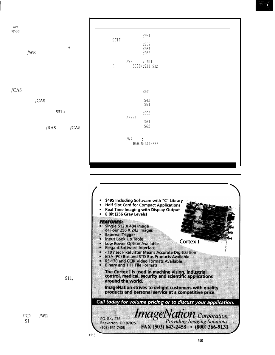
TRACE-ON PALCK ALE RD WR RAS MUX WE CAS ADCE Al5 Al4 PO P3 RESET
SETF
/ALE RD WR
RESET
CLOCKF
PALCK
SETF
/RESET
CLOCKF PALCK
PHASES BEFORE RD OR WR
SETF
ALE PSEN
CLOCKF PALCK
28
Issue
September 1994
The Computer
clock cycle later than /MUX) gives a
t
of 83 ns, so again is well within
The equation for the /WE signal
is:
/WE = CSDRAM * (S21 + S22 S31)
l
During a DRAM read, /WE is not
active. As shown in Figure 6, /WE
from the PAL is connected to /WE
inputs of the eight 41256 chips.
The last step involves asserting
and is done at the same time
during both read and write cycles. The
equation for
is:
CAS = CSDRAM * (S22 +
S32) +
REFCAS
Similar to the
signal,
is connected to all eight 41256 chips.
DRAM REFRESH TIMING
AND EQUATIONS
According to the DRAM specifica-
tion, the refresh rate has to be 256
times per 4 ms. That is, the refresh
must occur once every 4 us. Can this
be done using just software?
Executing M 0 V X instructions
continuously would result in DRAM
accesses every other machine cycle, or
once every 24 oscillator periods
(remember, there are 12 oscillator
periods per machine cycle). That
translates to an access every 2 us.
While we could conceivably keep
memory refreshed using this tech-
nique, it wouldn’t leave much time to
do any useful work. Let’s let the PAL
do the refresh for us.
The only time data memory is
accessed during the second machine
cycle of an instruction (as shown in
Figures 4 and 5) is with the MOVX
instruction. With all other instruc-
tions, the CPU never accesses data
memory during clock cycles
S12,
S21, and S22, so we can do our refresh
during these cycles. This technique is
known as cycle
stealing.
We need some way to detect when
instructions other than MOVX are being
executed so we can start a refresh
cycle.
and
can be active only
during l-S32 of the second machine
cycleofaMOVX,sowecanuse/RD=O
Listing l-continued
CLOCKF PALCK
/ALE
CLOCKF PALCK
CLOCKF PALCK
CLOCKF PALCK
SETF
PHASE COUNT AND WRITE TO DATA MEMORY
FOR I:= TO 6 DO
CLOCKF PALCK
END
SETF WR
FOR I := 1 TO 5 DO BEGIN
CLOCKF PALCK
FETCH OR PREFETCH
SETF
ALE PSEN
CLOCKF PALCK
CLOCKF PALCK
SETF
/ALE
CLOCKF PALCK
SETF
CLOCKF PALCK
CLOCKF PALCK
END
SETF
Al5 WRITE TO ADC
FOR I:= 1 TO 6 DO
CLOCKF PALCK
END
TRACE-OFF
/Video Frame Grabber
The Computer Applications Journal
Issue
September 1994
2 9
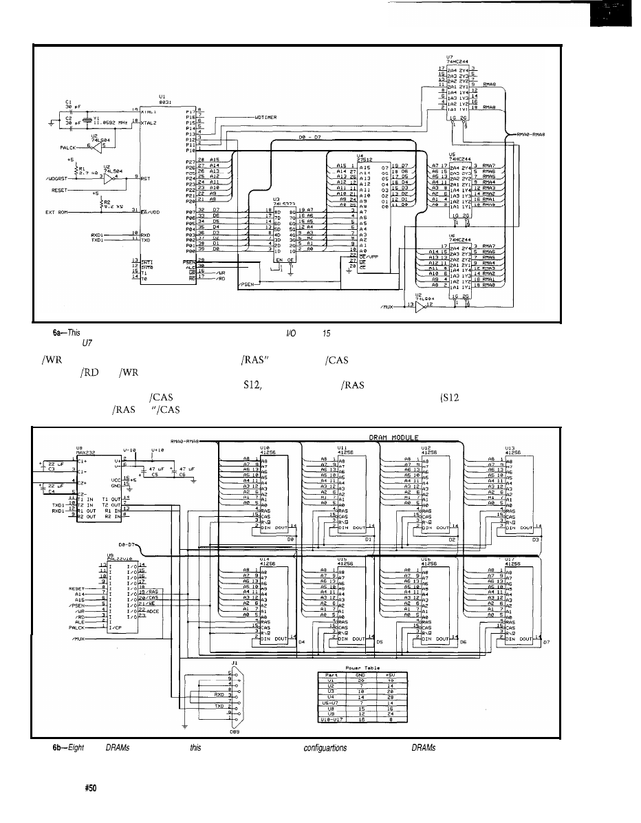
Figure
is a common 8031 circuit with a
DRAM address multiplexer. Three bits and address lines are used to generate the DRAM row and column addresses.
Six more pins on are available for further DRAM expansion.
or
= 0 to indicate “no refresh.”
before
refresh. The
equations for REFCAS and REFRAS
When both
and
are high, we
refresh signal, REFCAS, is active
are:
know we can perform a refresh.
during
S21, and S22. The
As I mentioned before,
has
refresh signal, REFRAS, is active
REFCAS =
+ S21 + S22) * RD *
to be active before
for
during S21 and S22. So the final
WR
Figure
41256
are implemented in
application. Other DRAM sizes or
(e.g., two 4 x 256 Kb
or DRAM modules) can be used with
minor modifications.
30
Issue
September 1994
The Computer Applications Journal
CPU States
s 3
s 4
s 5
S6
OSC Phases
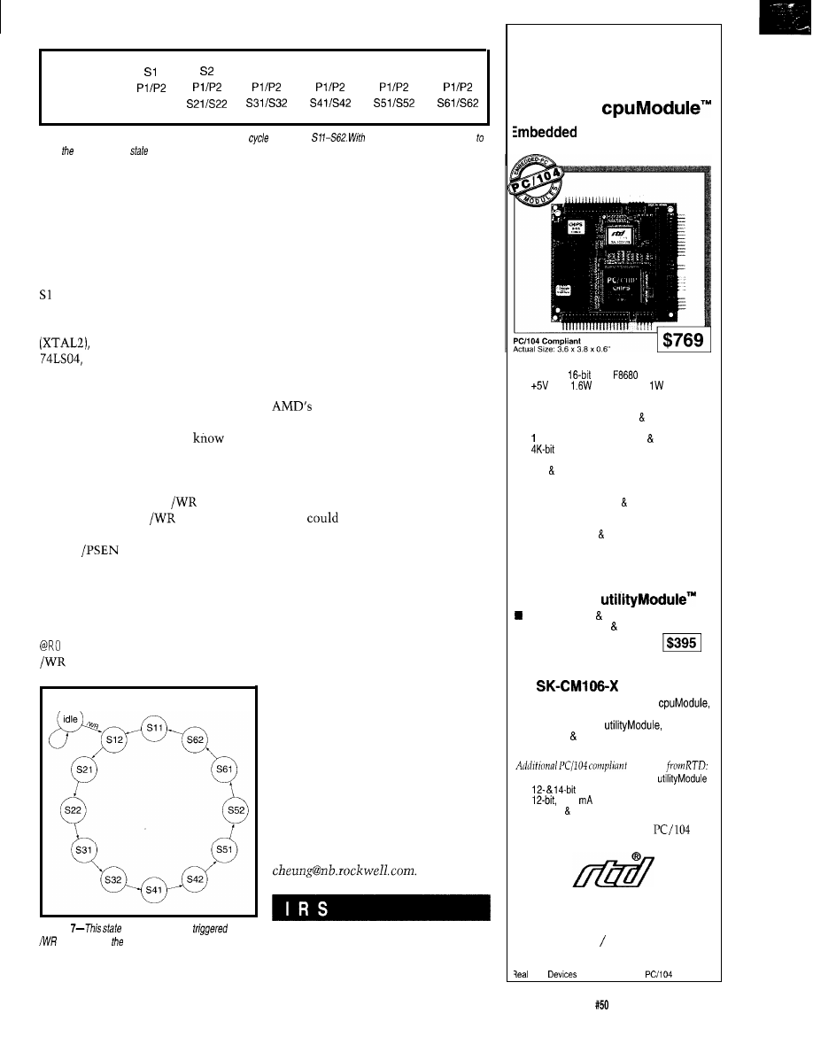
Detail States Sl l/S12
Table
l--The twelve states of
each
8031 machine
are named
these new names, if is easier
follow structure of fhe
machine and
PAL source code.
and
REFRAS = (S21 + S22) * RD * WR
OSCILLATOR CYCLE STATE
MACHINE
The 803 l’s twelve clock
states,
l-S62,
are tracked within the PAL
using a state machine (see Figure 7). 1
tap off the processor’s main oscillator
buffer the signal with a
and pass that signal to the
PAL to step the state machine on each
falling edge of the oscillator.
Now that 1 have a raw clock
input, how do 1 synchronize the state
machine with the CPU so 1
what
state the processor is in?
After the power-on reset, the state
machine is idle. It will exit its idle
state when it receives a
signal
from the processor.
is only active
on Sl 1, where other signals such as
ALE or
can be active during
multiple states (S12 or S42). Once
started, the state machine counts
through all the other states and
repeats. Your software must issue a
dummy instruction such
as “MOV X
,
A”
right after reset to generate a
signal and start the state counter.
Figure
machine, which is
by fhe
strobe, tracks CPU’s twelve machine cycles
and generafes DRAM read, write, and refresh control
signals.
In
order to avoid possible race
conditions and glitches in the PAL’s
latches that are used to count the state
machine, 1 use Gray code values.
Using Gray code, you are assured that
only one bit will change at a time
when stepping from one value to the
next.
The PAL’s reset input is con-
nected to the system reset, and, when
this signal is active high, the state
machine will be forced into an idle
state.
1 developed the PAL code using
PALASM and include a test
program in the source file.
IS
IT ENOUGH?
Ten years ago, when the Apple 11
was very popular, 64 KB of DRAM was
a lot of memory for applications of the
day. 1
run WordStar, Pascal, and
many other programs. Today, 1
complain about the 640 KB on my
being too small. In contrast, some
people may think that 256 KB or more
RAM for 803 1 is too much. However,
no matter how much memory the
hardware can provide, there are always
some applications, such as a printer
buffer or data logger, that will con-
sume it all and then some. So, good
luck on experimenting with beefing up
your DRAM.
q
Hugo Cheung is a Ph.D. student at the
University of Southern California and
is currently a systems engineer at
Rockwell Telecommunications
located in Newport Beach, CA. His
interests include embedded controls,
DSP applications, ASIC design, and
ASIC testing. He may be reached at
404 Very Useful
405 Moderately Useful
406 Not Useful
E
Replace Four
Conventional PC/l 04
Modules with
One
CMF8680
PC/XT Controller with
Intelligent Power Management
n PC/XT compatibility with 286 emulation
n 14 MHz,
C&T
CPU
n
only;
at 14.3 MHz,
at 7.2 MHz
n Intelligent sleep modes, O.lW in Suspend
n ROM-DOS and RTD enhanced BIOS
n Compatible with MS-DOS real-time
operating systems
n M bootable solid state disk free software
n
configuration EEPROM (2K for user)
n 2M on-board DRAM
n IDE floppy interfaces
n CGA CRT/LCD controller
n Two RS-232 ports, one RS-485 port
n Parallel, XT keyboard speaker ports
n Optional X-Y keypad scanning/PCMCIA
interface
n Watchdog timer real-time clock
Expand This Or Any PC/l 04 System
with the
CM106 Super VGA
Controller
Mono/color STN TFT flat panel support
n Simultaneous CRT LCD operation
n Resolution to 1024 x 768 pixels
n Displays up to 256 colors
Speed Product Development with the
Starter Kit
Your kit includes the CMF8680
CM106 SVGA controller, CM102 keypad
scanning/PCMCIA
CMF8680
cable kit VGA monitor cable for just
$1295.
modules
n CM104 1.8” hard drive carrier
n
analog I/O modules
n
4-20
analog output modules
n opto-22 digital I/O modules
For more information on our
and
ISA bus products, call today.
Real Time Devices USA
200 Innovation Blvd.
l
P.O. Box 906
State College, PA 16804 USA
(814) 234-8087 Fax: (814) 234-5218
RTD Europa
l
RTD Scandinavia
Time
is a founder of the
Consortium.
16
The Computer Applications Journal
Issue
September 1994
31
with heightened capabilities.
These new products will offer through-
out the decade a multitude of choices
for system designers in all areas of the
embedded control marketplace.
In the past, general-purpose
microprocessors were integrated into
embedded designs with little insight
from microprocessor manufacturers
about how to improve the overall
system. Today, microprocessor
designers are looking for the balance
between a set of features, cost, and
design cycle time while system
designers seek more performance at a
lower system cost.
The 68322 is an example of
Motorola’s response to the needs of the
embedded control market. The chip is
the first of Motorola’s 68000 family
microprocessors specifically designed
to redefine the low-end laser printer
market.
The market for laser printers is
composed of three segments: high-end,
mid-range, and low-end printers.
end printers use high-performance
for enhanced networking
capability, higher resolution, and,
most importantly, faster printing. As
the price of high-end printers drops,
Ron
Motorola’s 68322 Processor:
Redefining the Low-end
Laser Market
improvements in
industry are changing
the embedded system environment of
the ’90s. Key microprocessor manufac-
turers are introducing with an
increasing intensity integrated
Photo
squeezing more onto a single piece of silicon, Motorola hopes further drive down the price of
end laser printers.
34
Issue
September 1994
The Computer Applications Journal
Figure
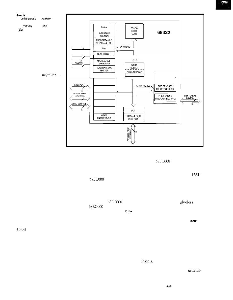
68322 uses a dual-bus, dual-
processor
a/so
IEEE-
/284 parallel port, printer engine, DRAM
interfaces to
eliminate need for
external
logic.
and low-end printers gain more
power and additional features,
manufacturers of mid-range laser
printers are challenged to
compete with lower prices and
additional features.
A fourth market
Windows printing or graphics
device interface (GDI)-will
emerge in 1994. Manufacturers
in the GDI market will integrate
a less powerful processor in a
laser printer which will rely on a
host computer for much of the
CPU-intensive rasterization. The
host computer will generate a
bitmap image or an image
composed of low-level graphic
commands that will be down-
loaded to the GDI laser printer
for printing.
DATA ,
16
ADDRESS ,
,
20
INTERFACE CONTROL
I I
UNIT
A
GRAPHICS EXECUTION
RAS (6)
UNIT (GEU)
CONTROL
CAS (2)
CONTROL
BURSTING
LOGIC
MULTIPLEX
ADDRESS
REFRESH
CONTROL
68322 TECHNICAL
INFORMATION
The integrated laser printer
microprocessor, 68322, is designed
specifically for the GDI and low-end
laser printer markets. Several key
features make the 68322 well-suited
for personal printers.
Figure 1 shows the general layout
of the 68322. With a true dual-bus,
dual-processor architecture, the 68322
fetches instructions for the 68ECOO0
core from the 68322 bus while the
graphics bus performs operations on
text and graphics images in the DRAM
from the second bus. This feature
provides a significant performance
improvement while operating from the
dual
buses. A specialized
graphics accelerator is on the chip to
interpret graphics commands known
as display lists. The graphics unit is
divided into a RISC graphics processor
(RGP), which executes or interprets
graphics commands from DRAM, and
a print engine video controller, which
handles the print engine interface and
video transfers from DRAM to the
print engine.
being initialized, the RGP interprets
The RGP is a powerful accelerator
the display list and creates a page, one
band at a time, with no intervention
containing several registers. After
from the
processor. The print
engine video controller acts as an
intelligent DMA unit transferring the
video from DRAM to an internal FIFO
and out the video port without
interaction from the
proces-
sor. The
processor com-
presses the video image using a
length encoded (RLE) compression
technique. The RGP automatically
decompresses the video, and the print
video controller sends the data to the
print engine. These dedicated features
remove the burden from the processor
and use dedicated hardware to dra-
matically improve performance and
reduce system cost.
video controller, and two DMA units.
A single DMA unit is dedicated to the
print engine. The DRAM bus is shared
support of a bidirectional, IEEE-
with the
core, RGP, print
compatible, parallel communication
port. The second DMA channel
transfers data between the processor
bus and the DRAM bus.
Modifications to the 68000
processor bus result in a
interface to virtually all peripherals.
For example, separate read-and-write
strobes are added to the system
integration module to support
Motorola peripherals. The chip selects
are programmable to provide indi-
vidual setup-and-hold and recovery
times for each of the eight banks.
The 68322 video interface requires
no external glue logic to interface with
most laser printer engines. The 68322
is so versatile that it can be used in
facsimile machines, and even
in nongraphics applications that
require DMA, DRAM
S
, and a
purpose 68000 processor.
The bursting DRAM interface
supports CPU data structures, graphics
rendering, bit-block transfers, DMA
transfers, and display list interpreta-
tion while transferring video to the
The Computer Applications Journal
Issue
September 1994
3 5
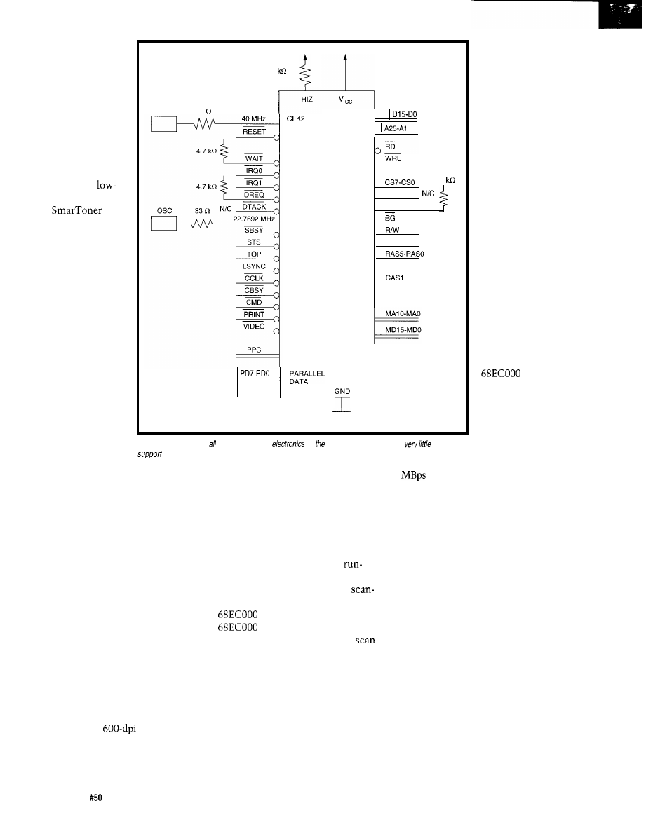
In addition, the
68322 has new
environmental green
features designed
into the device. The
68322 uses a new
static 68000 core
processor. With the
ability to stop the
clock, the device
will lend itself to
hand-held and
power applications.
The
option has been
designed into the
68322 to reduce the
amount of toner
applied to the page
when printing in a
draft mode.
THEORY OF
OPERATION
The primary
advantage of the
68322 processor is
its capability to
reduce the amount
of memory (one of
the most costly
devices in a laser
printer) required to
print a page. The
4.7
HIZ
o s c
33
RESET
D A T A
A D D R
CHIP SELECT
V C L K
W R L
4.7
A S
BR
N C
DTACK
NIC
-
-
CASO
W E
DRAM ADDR
DRAM DATA
PARALLEL PORT
CONTROL
I
DL410
_
Figure 2-By including the most-needed
on chip, the 68322 requires
external
circuitry
68322 features banding and video
image compression to ultimately
reduce manufacturing and consumer
costs--two major considerations when
designing for the low-end laser printer
market.
Banding allows the raster image
processor (RIP) board to
store
the page
in data strips. When banding, a full
page does not reside in memory at one
time. Instead, the video image con-
sumes only two bands of memory.
These bands range in size from less
than 10 KB to a full page. Typically, a
band is 32-64 KB. The 68322’s RGP
interprets the display list or graphics
orders into a band of video image. By
using a banding technique, the printer
dramatically reduces the memory
required to print a page. The 68322
prints a banded
page at full
speed, 6-8 ppm, using less memory
than conventional printers. Roughly 1
MB of memory is required to hold the
rasterized data of a single page at 300
dpi. When the resolution increases to
600 dpi, approximately 4 MB are
required if there is no memory com-
pression or banding.
The 68322 uses an additional
memory compression technique
known as scan-line tables or
length encoding, which compresses
repetitive rasterized data. The
line tables are not possible without the
and the versatile RGP. The
creates the compressed data,
and the RGP decompresses the
line tables on the fly.
For the 68322 to provide the
maximum performance of 8 ppm at
600 dpi, a significant amount of data
must be manipulated in real time. A
process known as
race the laser
requires the printer controller board to
translate display-list graphics orders
into a banded, rasterized bitmap
image as fast as the printer can place
the pixels on the
page.
To successfully
print from banded
memory, three
conditions must
exist. First, the
system must read
the complete display
list, place the
banded, rasterized
data into memory,
and then retrieve the
rasterized data in
real time to send to
the print engine.
The list of instruc-
tions and data to be
manipulated for
printing a page is
very long, resulting
in a potential
problem with bus
bandwidth. Because
the 68322 has a dual
bus architecture, the
core can
simultaneously
fetch instructions
for rasterization and
video data manipu-
lation.
The DRAM bus
bandwidth is 16
at 20 MHz. The data manipula-
tion required to band a page at 600 dpi
is approximately 24-40 MB of data. At
600 dpi and 8 ppm, a page prints every
7.5 s. The resulting bus utilization is
approximately 2033 %, providing
ample margin for time-critical func-
tions.
The second condition required for
printing from banded memory is that
the RGP must be capable of reading
the display list and interpreting
graphics commands fast enough to
keep up with the video-pixel data
being sent to the print engine. To print
a page, the RGP must interpret the
display list in real time and generate
the rasterized data for a complete
band. This action must transpire in the
amount of time it takes to transfer the
preceding band of video data to the
print engine.
The third condition is the reduc-
tion of required memory by the
36
Issue
September 1994
The Computer Applications Journal
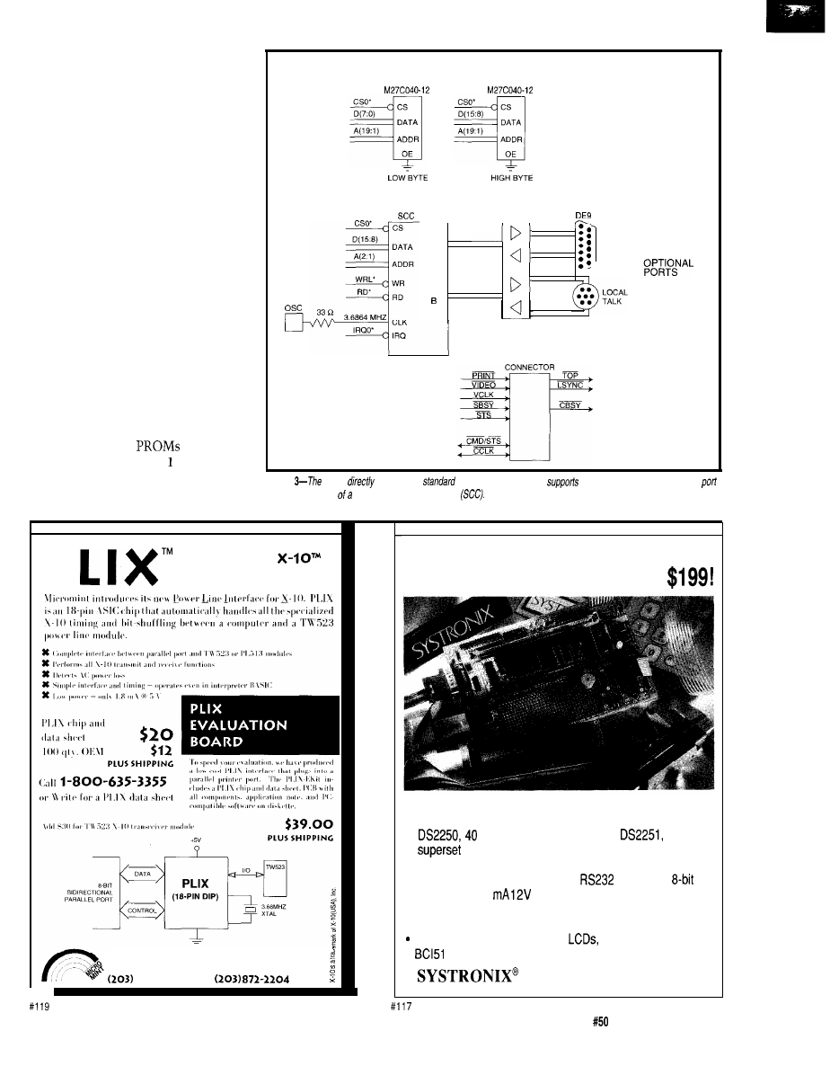
system. If memory and the resulting
cost cannot be significantly reduced,
banding is not economical and not
worth the investment. When the page
cannot be printed in the banding
mode, the 68322 has the ability to exit
the banding mode and generate a
single band that happens to be a full
page in length. Additional memory can
be installed or a lower-resolution mode
can be used to complete a lengthy or
graphically intensive print job.
LASER PRINTER ON A CHIP
Designing for a laser printer is
similar to designing for other embed-
ded applications-designers must
include a processor, memory, peripher-
als, input stimulus, and output data.
What distinguishes a laser printer from
other applications is the amount of
code that must be executed and the
amount of required memory to
perform the task.
Currently, the
inside a
laser printer range from MB to more
than 2 MB, depending on the number
of available fonts and supported
68k Bus
EPROM
PORT
SERIAL
A
PORT
PORT
PRINT ENGINE
Figure
68322
supports
a
parallel
port, and also
a serial port
and
a LocalTalk
with the
addition
serial communications
chip
P
HARDWARE
TRANSCEIVER CHIP
M I C R O M I N T , I N C .
4
PARK ST., VERNON, CT 06066
871-6170 FAX:
NEW! UNIVERSAL DALLAS
DEVELOPMENT SYSTEM
from
l
It’s a complete single board computer!
l
One board accommodates any 40 DIP DS5000, 40 SIMM
SIMM DS2252, or 72 SIMM
8051
processor! Snap one out, snap another in.
l
Programs via PC serial port. Program lock & encrypt.
l
LCD interface, keypad decoder,
serial port,
ADC, four 300
relay driver outputs.
l
Power with 5VDC regulated or 6-13 VDC unregulated
l
Large prototyping area, processor pins routed to headers
Optional enclosures, keypads,
everything you need
l
Pro BASIC Compiler w/50+ Dallas keywords $399
TEL: 801.534.1017 FAX: 801.534.1019
555 South 300 East. Salt Lake City, UT, USA 84111
The Computer Applications Journal
Issue
September 1994
3 7
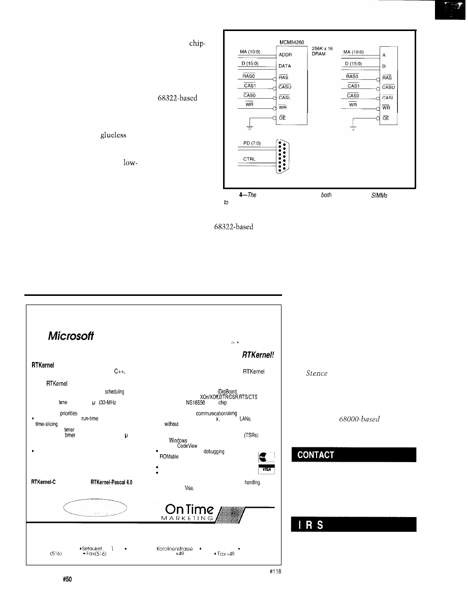
languages. Printers shipped today
include 512 KB to 16 MB of DRAM.
Communications options such as a
parallel port, LocalTalk, Ethernet, or
RS-232 are common. All print engine
controllers have a video port that is
typically serial.
The 68322 has integrated a
parallel port that complies with the
IEEE- 1284 specification and can be
directly connected to a host computer.
The DRAM interface is
with
RAS, upper and lower CAS strobes,
write enable, multiplexed addresses,
automatic incrementing of the
order address bits, memory decoding,
and automatic refresh.
The system integration module
(SIM) has a timer, prioritized processor
chip selects, byte-write enables, and a
separate read strobe to provide direct
connections to virtually any peripheral
or SRAM found in printers on the
market today. The SIM chip selects
can be individually programmed for
hold and recovery times and can be set
up with automatic termination,
providing a tremendous amount of
DRAM SIMM
flexibility to the
processor
select logic.
Figures 2, 3,
and 4 describe
the logic required
for a typical
laser
printer. Printer
manufacturers
provide various
configurations of
base memory and
communications.
The 68322
provides the chip
select with a
versatile DRAM
interface to meet
the many
demands of a constantly changing
printer market. A
design
redefines the entry-level laser printer
available on the market today. The
68322 innovations will reduce laser
printer manufacturing costs while
improving the performance and
resolution.
PARALLEL
PORT
Figure
68322 also directly supports
DRAM chips and
in addition
printer engines.
AN EMBEDDED FUTURE
The microprocessor industry is
moving to meet the demands of the
evolving printer marketplace. Micro-
processor manufacturers are under
increasing pressure to be the first to
develop new and innovative solutions
for the embedded market. Increasing
integration and performance will
become the norm from the major
microprocessor design houses. The
68322 provides large-scale integration,
a significant increase in performance,
and reduces system cost. It provides
a strong option for laser printer
designs.
q
Real- Time Multitasking with DOS
for
C, Borland C, Borland/Turbo Pascal
Develop Real-Time Multitasking Applications under MS-DOS with
is a professional, high-performance real-time multitasking kernel. It runs under MS-DOS
or
in ROM
and supports Microsoft C, Borland
Borland/Turbo Pascal, and Stony Brook Pascal+.
is a
library you can link to your application. It lets you run several C functions or Pascal procedures as parallel
tasks.
offers the following advanced features:
l
pre-emptive, eventiinterrupt-driven
l
number of tasks only limited by available RAM
l
supports up to 36 COM ports
Hostess boards)
l
supports protocols
l
task-switch
of approx. 6 s
466)
l
performance is independent of the number of tasks
l
use up to 64
to control your tasks
priorities changeable at
l
can be activated
l
programmable
interrupt rate (0.1 to 55 ms)
l
full support of
UART
l
supports math coprocessor and emulator
l
fast, inter-network
Novell’s IPX
l
runs under MS-DOS 3.0 to 6 DR-DOS,
or
operating system
l
high-resolution
for time measurement (1 s)
l
DOS
calls from several tasks without re-entrance problems
l
activate or suspend tasks out of interrupt handlers
l
supports resident multi-tasking applications
l
runs
or DOS Extenders as a task
l
programmable interrupt priorities
semaphores, mailboxes, and message-passing
l
supports
and Turbo Debugger
l
keyboard, hard disk, and floppy disk idle times
Kernel Tracer for easy
l
usable by other tasks
l
full source code available
l
interrupt handlers for keyboard,
COM
ports, and
no run-time royalties
network interrupts included with source code
free technical support by phone or fax
4.0 $495
$ 4 4 5
International orders: add $30 shipping and
C Source Code: add $445
Pascal Source Code: add $375
Mastercard,
check, bank transfer accepted
Professional Programming Tools
In
North America, please contact:
On Time Marketing
88 Christian Avenue
NY 1733 USA
Phone
689-6654
689-l 172
Outside North America, please contact:
On Time Marketing
32 20357 Hamburg GERMANY
Phone
40 43 74 72
40 43 51 96
CompuServe 73313.3177
CompuServe 100140,633
Ron
is a senior systems
application designer at Motorola. In
addition to providing applications
support for 68000 products, Ron has
been currently focusing his efforts on
the design of a
laser
printer.
Motorola Literature Distribution
P.O. Box 20912
Phoenix, AZ 85036
407
Very Useful
408 Moderately Useful
409 Not Useful
38
Issue
September 1994
The Computer Applications Journal
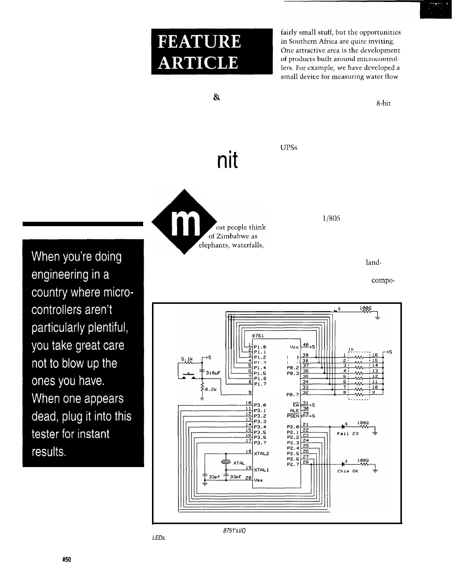
in rivers, which uses a fascinating
algorithm for salt dilution and conduc-
tivity. Parallel processing with
microcontrollers has been used, and
LAN controllers based on the same
chips have been investigated. On the
heavy current side, locally produced
use the same technology, and
U
work is in progress on the control of
electric motors. All of these are very
much “appropriate technology”
solutions to real problems that we
meet in this part of the world.
At the University of Zimbabwe,
Mike Collier
Fred Gweme
Preventing the Ultimate Blow:
A Portable Checking
for 8751s
rhino, and droughts. But
the electrical engineering students
study the 803
1
series of micro-
controllers, and a number of the
undergraduate and graduate research
projects use this family of devices.
The big difference between
behind these features which catch the
hardware development in a
eye of the media, there are other things
locked African country and that in the
going on. Among these is a growing
First World is accessibility of
electronics industry. At present it’s
nents. A development laboratory in
F a i l 0 1
PO.O
PO.l
P0.4
P0.5
P0.6
RESET
Figure l--The chip tester ties the
ports together for the diagnostics and reports its findings on three
40
Issue
September 1994
The Computer Applications Journal
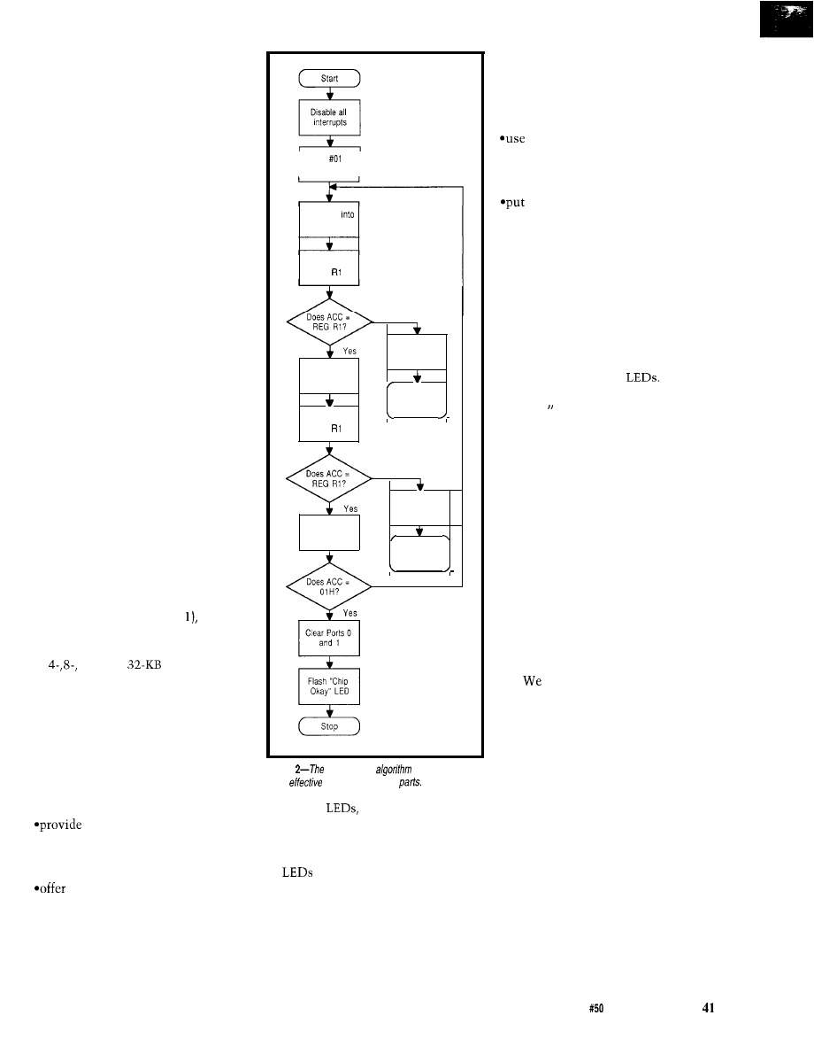
the U.S. or Europe would have an
unending supply of the crucial chips,
but here we often do development
with only one or two specimens in
hand. Inevitably, we meet the situa-
tion in which a prototype doesn’t
work, and the cry goes up, “The chip’s
blown.” At such a moment, one is
loathe to put the last chip in Zimba-
bwe into the circuit to see if it also
self-destructs!
To prevent such catastrophes, a
year ago we decided we needed a free-
standing tester that could quickly
check through all the functions of a
microcontroller. It had to be rugged,
portable, and “studentproof.” The
portability requirement did not mean
that it would be carried into the bush
on a safari; but, it did imply that the
unit should comprise a small box that
would function as soon as it was
turned on.
SPECIFYING THE MACHINE
Our experience with hard-luck
stories from students suggested that
most cases of damage to microcontrol-
lers resulted from incorrect voltages on
the pins. These errant voltages could
arise either from the malfunctioning of
circuits in which the device was
embedded or from static electricity
due to incorrect handling of the chips.
Since we were using the 875 1
(EPROM version of the 803
we
decided to build a tester specifically for
this family of chips, which now comes
in 16-, and
EPROM sizes.
We felt the most likely failure areas in
the 875 1 chip to be the EPROM and
the four I/O ports of 8 lines each. Since
the interrupts, timers, and serial port
all make use of particular lines of the
four ports, these would automatically
be covered by a general test of the I/O.
The tester needed to:
a circuit which would allow a
test program in the EPROM to
assess the major functions of the
device
connections to pairs of I/O pins
(preferably in different ports) which
would be tested sequentially by
using one pair for transmission of a
pulse train and the other for
reception
Move H
into ACC
Move ACC
Port 1
Move Port 0
into
N o
Clear Ports 2
and 3
Move ACC into
Port 2
Flash “Fail 01”
LED
Move Port 3
into
No
Clear Ports 0
and 1
Rotate ACC
Left
Flash “Fail 23
LED
No
Figure
basic testing
is quite simple,
but is
at weeding out bad
*output to
which would either
indicate failure of a port pair or a
successful test (the indicators must
signal failure of the pins driving the
when the test has failed)
To execute the general test procedure,
an individual should:
*download the standard test program
into the EPROM of the microcon-
troller (this could be achieved either
by use of a computer connected to
an EPROM programmer or by
copying the contents of an existing
EPROM into the microcontroller)
the programmer diagnostics to
verify the EPROM contents, thus
confirming the nonvolatile memory
to be intact
the chip into the functional tester
and power up
*observe the state of the LED indica-
tors to determine whether the ports
are functioning correctly
THE HARDWARE
Figure 1 shows the circuit of the
tester as it finally evolved. Pairs of
ports are connected for the I/O test
while other pins also provide the
driver circuitry for the
The three indicators are labeled as
“Fail 01, “Fail 23,” and “Chip OK,”
to signal the possible outcomes of the
test.
The tester includes a power
supply to provide the 5 V for the
operation of the 875 1.
THE TESTER SOFTWARE
The basic algorithm for the test
procedure is shown in the form of a
flowchart in Figure 2.
The test program was written in
ASM5 1 assembly language and is
given in Listing 1.
OUR EXPERIENCE WITH
THE SYSTEM
have used the tester over a
period of a year to enable students and
research workers to verify their
microcontrollers. In many cases in
which the students were vociferously
blaming the chip for having failed,
they subsequently found that the
problems lay in their circuitry or
software. Thus, the major benefit of
the tester lay in confirming that the
microcontroller was intact so that
troubleshooting could proceed in other
areas.
The stand-alone nature of the
tester has given it a high degree of
portability, which would not be the
case if we have made a computer-based
system. As a result, we have used a
single machine for people working on
The Computer Applications Journal
Issue
September 1994
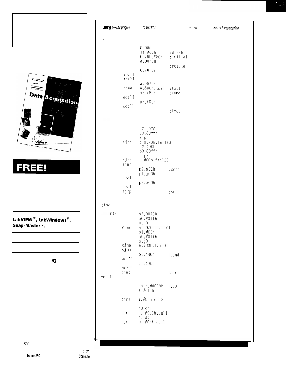
NEW Data
Acquisition
Catalog
Covers expanded
low cost line.
1994
120
page catalog
for PC, VME,
and Qbus data acquisition. Plus infor-
mative application notes regarding
anti-alias filtering, signal condition-
ing, and
more.
NEW Software:
and more
NEW Low Cost I/O Boards
NEW Industrial PCs
NEW Isolated Analog and
Digital Industrial
New from the inventors of
plug-in data acquisition.
Call, fax, or mail for your
free copy today.
is
used
microcontrollers
on/y
be
tester.
Main program
org
ptest:
mov
all interrupts
ports:
mov
test pin value
mov
tpin:
rl
a
one place left
mov
test23
test01
mov
finish:
for last port pin
mov
Chip OK signal
delay
mov
delay
sjmp
finish
on sending
subroutine to test port 2 and 3 pins.
test23:
mov
mov
mov
mov
mov
mov
ret23
fai123:
mov
chip fail signal
mov
delay
mov
delay
fail23
continuously
ret23:
ret
subroutine to test port 0 and 1 pins.
mov
fail01
delay:
dell:
de12
ADAC
American Data Acquisition Corporation
70 Tower Office Park, Woburn, MA
01801
Phone:
648-6589 Fax:
(617) 938-6553
42
September
1994
The
Applications
Journal
mov
mov
mov
mov
mov
ret01
mov
chip fail signal
delay
mov
delay
fail01
continuously
ret
mov
flashing delay
mov
dec
a
inc
dptr
mov
mov
ret
end
a
variety of projects. The tester can be
operated by people with limited
experience, mainly because of the
simplicity of the testing procedure and
the binary nature of the output
indicators.
Although the machine that we
have developed is intended for the
8751
chips only, the addition of a
separate EPROM containing the test
program would enable it to test the
803 1 and 805 1 microcontrollers since
they are not user-programmable.
With the radical changes taking
place in Southern Africa, we predict
that the market for electronic products
with a local flavor is going to increase.
Thus, devices of the type described
here will be needed to support elec-
tronic development initiatives and to
stimulate an industry which can be
independent and reliable.
q
Dr. Mike Collier and Mr. Fred Gweme
are both members
of staff
in the Elec-
trical Engineering Department at the
University of Zimbabwe. Mike
teaches software engineering, micro-
processor applications, and computer
engineering, and previously lectured
in Hong Kong and the U.K. Fred is a
Research Fellow in microcontroller
systems design. Both authors are com-
mitted to the development of engi-
neering within Zimbabwe. They may
be reached at
Jump S., Microcontroller Applica-
tions and Development,
4th Intl. Conf. on I.T.,
Gaberone, Botswana, May 1993.
Collier M. Gweme F., Develop-
ing an Intermediate Computer,
4th Intl. Conf. on I.T.,
Gaberone, Botswana, May 1993.
Collier M., A Low-Cost
Intensive Local Area Network,
‘92 Conference,
Swaziland, September 1992.
Embedded Controllers,
Intel,
1990, pp.
to 8-45.
410 Very Useful
411 Moderately Useful
412 Not Useful
HUGE BUFFER
FAST SAMPLING
SCOPE AND LOGIC ANALYZER
C LIBRARY W/SOURCE AVAILABLE
POWERFUL FRONT PANEL SOFTWARE
DSO Channels
2 Ch. up to 100
1 Ch. at
4K or 64K
Cross Trigger with LA
125 MHz Bandwidth
Logic Analyzer Channels
$1799 DSO-28204 (4K)
$2285 DSO-28264 (64K)
8 Ch. up to 100 MHz
4K or 64K
Cross Trigger with DSO
PAL
SAL
EEPROM
FLASH
EPROM
Free software updates on BBS
Powerful menu driven software
up
to 128 Channels
up to 400 MHz
up to
Samples/Channel
Variable Threshold Levels
8 External Clocks
16 Level Triggering
Pattern Generator Option
LA12100 (100 MHz, 24 Ch)
LA32200 (200 MHz, 32 Ch)
LA32400 (400 MHz, 32 Ch)
$2750 LA64400 (400 MHz, 64 Ch)
Link Instruments
369
Passaic Ave, Suite 100, Fairfield,
NJ 07004
fax:
808-8786
The Computer Applications Journal
Issue
September 1994
43
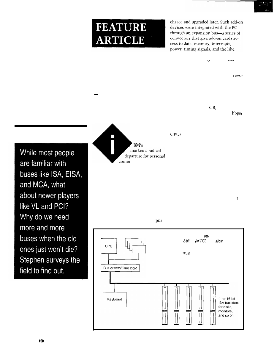
Just
why
the early IBM engineers
made this fateful design choice is a
Understanding PC Buses
question that will probably never be
answered, yet the impact of that deci-
sion sparked a personal computer
lution that continues today. In the
intervening 15 years, competition
between peripherals manufacturers has
given consumers high-performance,
photorealistic color video; storage
systems exceeding 2
modems that
can transfer data well above 14.4
and a host of other peripherals which
take advantage of a PC’s bus.
Stephen Bigelow
first PC
computer designs. Previ-
as
“add-on” devices that could be
ous computers incorporated key sys-
tems (video, storage, communications,
and so on) permanently into the
motherboard, but IBM chose to build a
motherboard containing only core
circuitry (the CPU, math coprocessor,
RAM, ROM, and glue logic). Functions
such as video adapters, serial and par-
allel ports, modems, floppy and hard
drive storage controllers were treated
With continuous improvements in
and other core logic, the PC
expansion bus has become a key factor
in the overall performance of a system,
New bus architectures are now appear-
ing that promise to keep pace with
future generations of PCs. This article
is intended present the architecture
and layout of today’s most popular PC
expansion buses.
ISA
The venerable Industry Standard
Architecture (ISA) shown in Figure
on the use of ISA buses (also referred
was the first open system bus architec-
ture used for personal computers.
Since there were no restrictions placed
Memory
Figure l--The original
PC and PC/XT used
the old
ISA
bus to
the use of
add-on expansion cards. The IBM PC/AT added
an extra connector to each slot to expand the
bus to
status.
ISA Bus
44
Issue
September 1994
The Computer Applications Journal
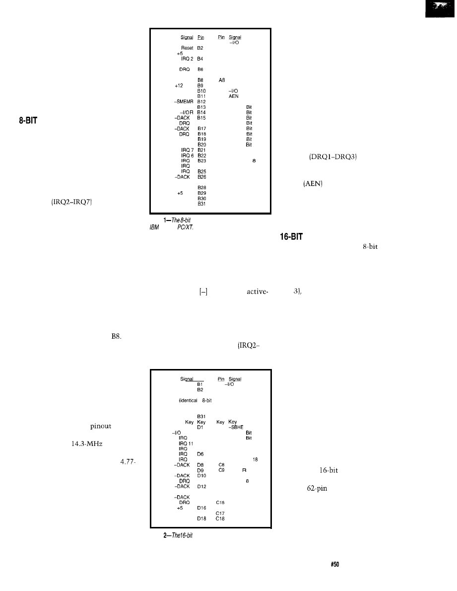
to
as “PC buses”), they were dupli-
cated in every IBM-compatible clone
that followed. Not only did the use of
a standard bus pave the way for thou-
sands of manufacturers to produce
compatible PCs and expansion devices,
but it also encouraged the use of stan-
dardized operating systems and appli-
cations.
ISA
Use of the S-bit XT bus started in
1982. The S-bit ISA bus consisted of a
card-edge connector with 62 contacts.
The bus provided eight data lines and
twenty address lines which enabled
the board to reside within the XT’s 1
MB of conventional memory. The bus
also supported connections for six
interrupts
and three
DMA channels and ran at a system
speed of 4.77 MHz. Although the bus
itself was relatively simple, IBM failed
to publish specific timing relationships
for data, address, and control signals.
This ambiguity left early manufactur-
ers groping to find proper timing rela-
tionships by trial and error.
Although each connector on the
bus was supposed to work the same,
early PCs designed with eight expan-
sion slots required any card inserted in
the eighth slot (the slot closest to the
power supply) to provide a special
“card-selected” signal on pin
Tim-
ing requirements for the eighth slot
were also tighter. Contrary to popular
belief, the eighth slot had nothing to
do with IBM’s expansion chassis. The
demands of slot 8 were for support of a
keyboard/timer adapter board for
IBM’s special configuration called the
3270PC. Most XT clones did not ad-
here to this “eighth slot” peculiarity.
Table 1 shows the
for an
XT-bus configuration. The oscillator
pin provides the
system
oscillator signal to the expansion bus,
while the clock pin supplies the
MHz system clock signal. When the
PC needs to be reset, the RESET DRV
pin sets the whole system into a reset
state. The twenty address pins (O-19)
connect an expansion board to the
system’s address bus. The eight data
lines (O-7) connect the board to the
system’s data bus. When address sig-
nals are valid, the address-latch-enable
Ground
B l
VDC
-5 VDC
2
-12 VDC
-Card Selected
VDC
Ground
-SMEMW
-I/O w
3
3
1
1
-REFRESH
Clock (4.77 MHz)
5
4
3
2
T/C
BALE
VDC
Osc (14.3 MHz)
Ground
B3
B5
B7
B16
B24
B27
A l
A2
A3
A4
A5
A6
A7
A9
A l 0
A l l
A l 2
A l 3
A l 4
A l 5
A l 6
A l 7
A l 6
A l 9
A20
A21
A22
A23
A24
A25
A26
A27
A26
A29
A30
A31
CHCK
Data Bit 7
Data Bit 6
Data Bit 5
Data Bit 4
Data Bit 3
Data Bit 2
Data Bit 1
Data Bit 0
CHRDY
Address Bit 19
Address
18
Address
17
Address
16
Address
15
Address
14
Address
13
Address
12
Address
11
Address Bit 10
Address Bit 9
Address Bit
Address Bit 7
Address Bit 6
Address Bit 5
Address Bit 4
Address Bit 3
Address Bit 2
Address Bit 1
Address Bit 0
Table
ISA bus was used on the original
PC and
signal indicates that the address may
now be decoded.
The I/O Channel Check (-I/
OCHCK) flags the motherboard when
errors occur on the expansion board
(the minus sign indicates an
low signal). The I/O Channel Ready
(-I/O CHRDY) is active when an ad-
dressed expansion board is ready. If
this pin is logic 0, the CPU will extend
the bus cycle by inserting wait states.
The six hardware interrupts
IRQ7) are used by the expansion board
P
i
n
G r o u n d
Al
C H C K
Reset
A2 Data Bit 7
to
bus in Table 1)
Osc (14.3 MHz)
Ground
-MEM CS16
CS16
D2
10
D3
12
15
14
0
DRQ 0
5
5
6
DRQ 6
7
7
VDC
-MASTER
Ground
B30
D4
c 4
D5
c 5
C6
D7
c 7
C l 0
D l l
Cl1
C l 2
D13
C l 3
D14
C l 4
D15
C l 6
D17
A30
A31
C l
c 2
c 3
Address Bit 1
Address Bit 0
Address
23
Address
22
Address Bit 21
Address Bit 20
Address Bit 19
Address Bit
Address Bit 17
-MEM
-MEM W
Data Bit
Data Bit 9
Data Bit 10
Data Bit 11
Data Bit 12
Data Bit 13
Data Bit 14
Data Bit 15
Table
ISA bus is identical to the B-bit ISA
bus, but adds a second connector with more signals.
to
demand the CPU’s attention. Inter-
rupts 0 and 1 are not available to the
bus since they handle the highest
priorities of the timer chip and key-
board. The I/O Read (-I/O R) and I/O
Write (-I/O W) indicate that the CPU
or DMA controller want to transfer
data to or from the data bus. The
Memory Read (-MEMR) and Memory
Write (-MEMW) signals tell the expan-
sion board that the CPU or DMA con-
troller is going to read or write data to
main memory.
The XT bus supplies three DMA
Requests
thereby en-
abling an expansion board to transfer
data to or from memory. If the Address
Enable
signal is true, the DMA
controller is controlling the bus for a
data transfer. Finally, the Terminal
Count (T/C) signal provides a pulse
when DMA transfer is complete.
ISA
The limitations of the
ISA
bus were soon obvious. With the
floppy and hard drives taking up two of
the six available interrupts, COM3 and
COM4 taking another two (IRQ 4 and
IRQ and an LPT port taking IRQ 7,
competition for the remaining inter-
rupt was fierce. Of the three DMA
channels available, the floppy and hard
drives take two-only one DMA chan-
nel remains available. Since only 1 MB
of address space is addressable, 8 data
bits form a serious bottleneck for data
transfers. Although it would have been
a simple matter to start from scratch
and design an entirely new bus, that
would have made the entire installed
base of XT owners obsolete.
The next logical step in bus evolu-
tion came in 1984 and ‘85 with the
introduction of the 80286 in IBM’s
PC/AT. System resources were added
to the bus which still allowed XT
boards to function in the expanded
bus. The result became what we know
today as the
AT bus. Instead of
using a different bus connector, the
original
connector was left
intact, and an extra 36-pin connector
was added (see Table 2) and designated
C and D. As well, an extra eight data
bits were added to bring the total data
bus to 16 bits, and five interrupts and
four DMA channels were included.
The Computer Applications Journal
Issue
September 1994
4 5
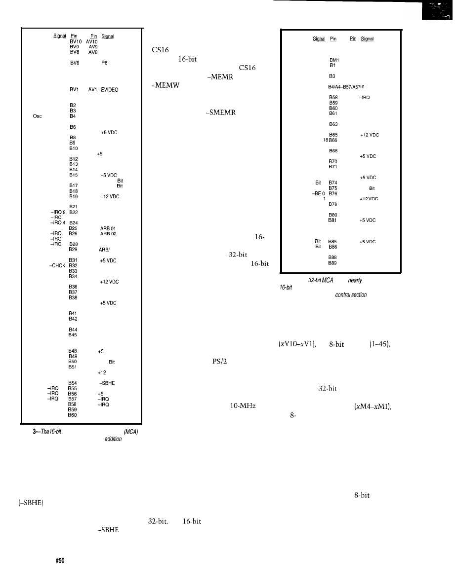
G r o u n d
P 5
ESYNC
P4 BV7
P 3
Ground BV5
P2 BV4
P l B V 3
PO BV2
G r o u n d
Key Key
AUDIO Ground Bl
A U D I O
G r o u n d
(14.3 MHz)
Ground B5
Address Bit 23
Address Bit 22 B7
Address Bit 21
G r o u n d
Address Bit 20
Address Bit 19 Bll
Address Bit 18
G r o u n d
Address Bit 17
Address Bit 16
Address Bit 15 B16
G r o u n d
H S Y N C
B L A N K
AV7 Ground
V S Y N C
A V 6
AV5 EDCLK
AV4 DCLK
AV3 Ground
A V 2 P 7
Key Key
Al -CD Setup
A 2 M A D E 2 4
A3 Ground
A4 Address Bit 11
A5 Address Bit 10
A6 Address Bit 9
A 7
A8 Address Bit 8
A9 Address Bit 7
Al0 Address Bit 6
All
V D C
Al2 Address Bit 5
Al3 Address Bit 4
Al4 Address Bit 3
A l 5
Al6 Address
2
Al7 Address
1
Al8 Address Bit 0
A 1 9
A 2 0 - A D L
A21 -PREEMPT
A22 -BURST
A 2 3 - 1 2 V D C
A24 ARBOO
A 2 5
A 2 6
A 2 7 - 1 2 V D C
A 2 8 A R B 0 3
A29
-GNT
A 3 0 - T C
A 3 1
A 3 2 - S O
A 3 3 - S l
A34 M/-l/O
A 3 5
A36 CD CHRDY
A37 Data Bit 0
A38 Data Bit 2
A 3 9
A40 Data Bit 5
A41 Data Bit 6
A42 Data Bit 7
A43 Ground
A44 -DS 16 RTN
A45 -REFRESH
Key Key
Key Key
A48
VDC
A49 Data Bit 10
A50 Data
11
A51 Data Bit 13
A52
VDC
A53 Reserved
A 5 4
A55 -CD DS 16
A56
VDC
A57
14
A58
15
A59 Reserved
A60 Reserved
Address Bit 14
Address Bit 13
Address Bit 12 B20
G r o u n d
3 B23
G r o u n d
5
6 B27
7
G r o u n d
Reserved B30
Reserved
G r o u n d
- C M D
CHRDYRTN B35
-CD SFDBK
G r o u n d
Data Bit 1
Data Bit 3 B39
Data Bit 4 B40
G r o u n d
CHRESET
Reserved B43
Reserved
G r o u n d
Key Key
Key Key
Data Bit 8
Data Bit 9
G r o u n d
Data Bit 12
Data Bit 14 B52
Data Bit 15 B53
G r o u n d
10
11
12
Ground
Reserved
Reserved
Table
Micro Channel Architecture
bus includes audio and video signals in
to
typical bus signals.
Four more address lines were also
provided in addition to several more
control signals. Clock speed was in-
creased on the AT bus to 8.33 MHz.
The System Bus High Enable
is active when the upper eight
data bits are being used. If the upper
eight bits are not being used (i.e., an
XT board in the AT slot),
will
be inactive. If the expansion board
requires 16-bit access to memory loca-
tions, it must return an active -MEM
signal. If the expansion board
requires
access to an I/O loca-
tion, it must make the -I/O
signal active. The
and
signals provided by an expan-
sion board tell the CPU or DMA con-
troller that memory access is needed
up to 16 MB. The
and
-SMEMW signals only indicate
memory access for the first 1 MB. The
-MASTER signal can be used by ex-
pansion boards that are able to take
control of the bus through use of a
DMA channel. It is interesting to note
that small, highly integrated AT sys-
tems are available for embedded sys-
tems and dedicated applications.
MCA
With the introduction and wide-
spread use of 32-bit microprocessors
such as the 80386 and 80486, the
bit ISA bus again faced a data through-
put bottleneck. Passing a
word
across the expansion bus in two
halves presented a serious waste of
valuable processing time. Not only
were data and CPU speed an issue, but
video and audio systems in PCs had
also improved. By early 1987, IBM
concluded that it was time to lay the
ISA bus to rest, and to unleash an
entirely new bus structure which it
dubbed the Micro Channel Architec-
ture (MCA). IBM incorporated the
MCA bus into their
series of
personal computers and their System/
6000 workstations.
MCA offers plug-in audio and
video capability, bus arbitration for
sophisticated peripherals,
operation for high data throughput,
and automatic setup configuration.
Although MCA offers many enhance-
ments over the ISA bus, computer
users are refusing to abandon their
hardware and software investment to
scramble for limited MCA-compatible
peripherals to fill their needs. As a
result, the MCA bus has not become
the standard IBM hoped it would be.
There are two major types of MCA
slots: 16-bit with video extensions and
The
MCA slot is shown
in Table 3. It is a primary type of MCA
connector which combines video and
Ground BM4
Reserved BM3
- M M C R B M 2
Reserved
AUDIO Ground
AUDIO B2
G r o u n d
AM4 Reserved
AM3 -MMC CMD
AM2 Ground
A M 1 - M M C
Al -CD Setup
A 2 M A D E 2 4
A3 Ground
(Identical to
Table 3)
G r o u n d
A58
15
Reserved
A59 Reserved
Reserved
A60 Resewed
Reserved
A61 Ground
Reserved B62
A62 Reserved
G r o u n d
A63 Reserved
Data Bit 16 B64
A64 Reserved
Data Bit 17
A 6 5
Data Bit
A66 Data Bit 19
Ground B67
A67 Data Bit 20
Data Bit 22
A68 Data Bit 21
Data Bit 23 B69
A 6 9
Reserved
A70 Data Bit 24
G r o u n d
A71 Data Bit 25
Data Bit 27 B72
A72 Data Bit 26
Data Bit 28 B73
A 7 3
Data
29
G r o u n d
A74 Data Bit 30
A75 Data
31
A76 Reserved
- B E B 7 7
A 7 7
- B E 2
A 7 8 - B E 3
Ground B79
A79 -DC 32 RTN
T R 3 2
A80 -CD DS 32
Address Bit 24
A 8 1
Address Bit 25 B82
A82 Address Bit 26
Ground B83
A83 Address Bit 27
Address Bit 29 B84
Address
30
Address
31
Ground B87
Reserved
Reserved
A84 Address Bit 28
A 8 5
A86 Reserved
A87 Reserved
A88 Reserved
A89 Ground
Table 4-The
bus is
identical to the
version, but rep/aces the video section with a
smaller matched memory
and includes
additional address and data lines.
audio signals in the expansion bus.
The connection itself can be divided
into three sections: the video section
the
section
and the 16-bit section (48-58). Power,
ground, and interrupt lines are easy to
spot, but most other signals are new.
The 32-bit MCA slot is shown in
Table 4. The
bus replaces the
video section with a smaller matched
memory control section
but and 16-bit sections remain the
same. The 32-bit MCA slot also in-
cludes a 32-bit section (59-89).
Enable Synchronization (ESYNC)
controls VGA signals on the mother-
board. When ESYNC is true, the Verti-
cal Synchronization (VSYNC), Hori-
zontal Synchronization (HSYNC), and
Blanking (BLANK) signals control the
display. An independent
video
data bus (PO-P7) supports 256 colors
on the VGA display. VGA timing sig-
nals are controlled by the Enable Data
Clock (EDCLK) and Data Clock
(DCLK) signals. The Enable Video
46
Issue
September 1994
The Computer Applications Journal
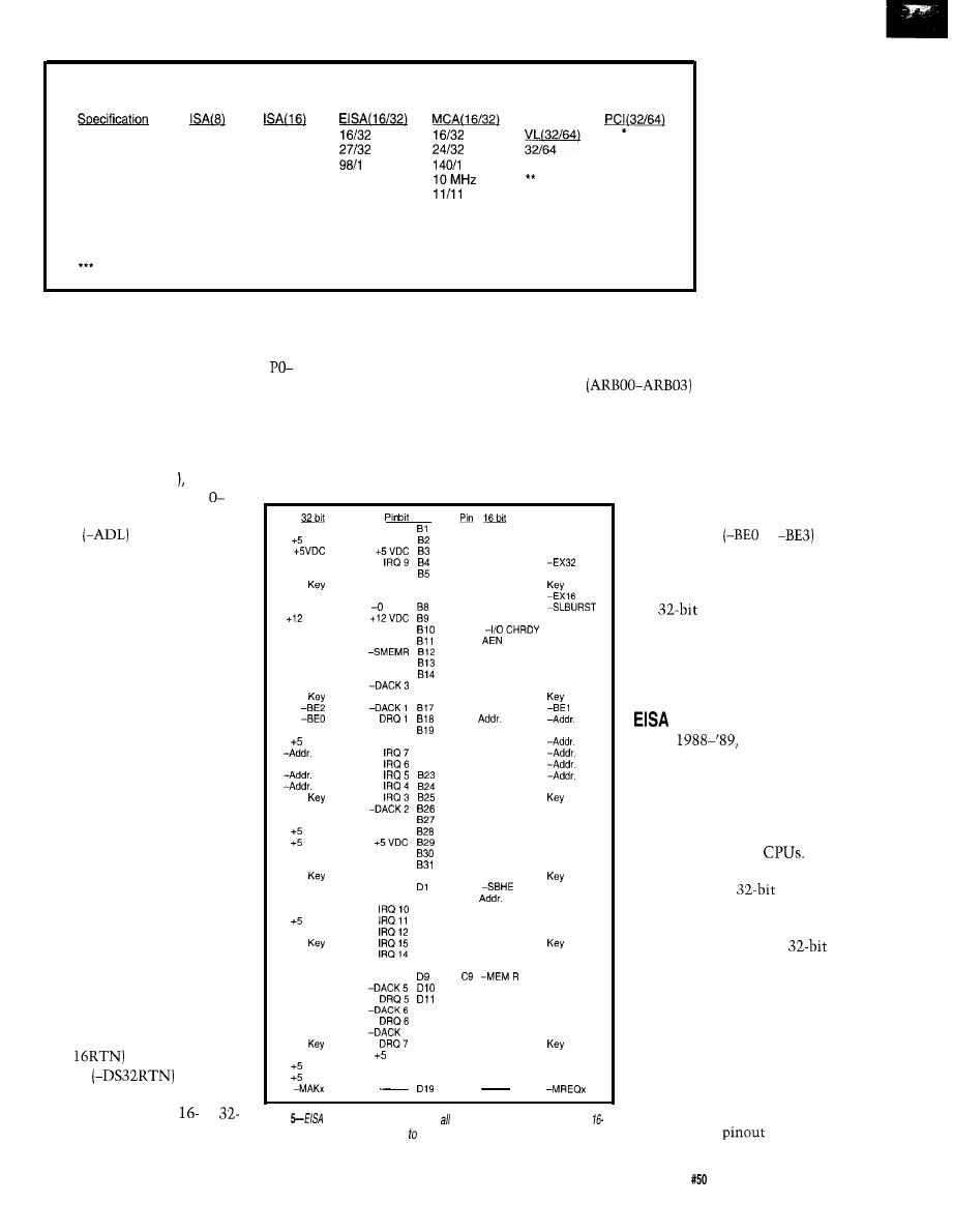
BUS SPECIFICATION COMPARISON
Data Bus
8
16
64
Address Bus
20
27
32
64 *
Bus Pins
62
98
00
82
116
188 (w/keys)
Clock Speed
4.77 MHz
8.33 MHz
8.33 MHz
33 MHz
Interrupts
6
11
11
1
4
DMA Channels
3
7
7
none***
none***
none***
*
address and data lines are multiplexed on the same conductors
**
depends on the speed of the host computer
bus mastering used
(EVIDEO) signal switches control of
the palette bus enabling an external
video adapter to provide signals on
P7. Audio [AUDIO) and Audio Signal
Ground (AUDIO Ground) enable the
expansion board to send tone signals to
the motherboard speaker.
High Enable (SBHE) signal is true
The Preempt (-PREEMPT) signal
when the upper 16 data bits are being
is true when a bus arbitration cycle
used, but the Card Data Size 16
begins. The Arbitration signals
(CDDS16) signal is true when only 16
indicate which of the
data bits are being used. If all 32 bits of
16 possible bus masters has won arbi-
data are being transferred, the Card
tration. The Arbitration or Grant
Data Size 32 (-CDDS32) signal is true.
(ARB/-GNT) is high when the bus is
When main memory is refreshed, the
in arbitration, and low when bus con-
Refresh (-REF) line is true. This allows
trol has been granted. When a DMA
Ground
VDC
Reserved
Reserved
There are 32 address bits (Address
Bit O-Address Bit 3 1 11 interrupts,
and 32 data bits (Data Bit
Data Bit 3
1).
The Address
Latch
signal is true
when a valid address exists on
the address lines. A Channel
Check (-CHCK) signal flags
the motherboard when an error
is detected on the expansion
board. When data on the data
bus is valid, the Command
(-CMD) is true. The Channel
Ready Return (CHRDYRTN)
signal is sent to the mother-
board when the addressed
expansion board I/O channel is
ready. A Channel Reset
(CHRESET) signal can be used
to reset all expansion boards.
The Card Setup (-CDSETUP)
instructs an addressed board to
perform a setup. The Memory
Address Enable 24 (MADE24)
line activates address line 24.
After completing its access, the
Channel Ready (CHRDY) line
indicates that the addressed
board is idle. When Burst
(-BURST) is true, the system
bus executes a burst cycle.
16
Ground
Reset
- 5 V D C
D R Q 2 B 6
3
2
Al -I/O CHCK
- C M D
A2 Data 7
-START
A3 Data 6
EXRDY
A4 Data 5
A5 Data 4
Ground
A6 Data 3
Reserved
Reserved
VDC
M -I/O
-LOCK
Reserved
Ground
Reserved
-BE3
Ground
-REFRESH
VDC Clock (8.33 MHz) B20
29
B21
Ground
B 2 2
26
24
- 1 2 V D C B 7
A7 Data 2
WAIT
A8 Data 1
A9 Data 0
-MSBUFiST
Ground
A 1 0
W - R
- S M E M W
A l l
Ground
Al2 Addr. 19
Reserved
-I/O W
Al3 Addr. 18
Reserved
- I / O R
Al4 Addr. 17
Reserved
B 1 5
Al5 Addr. 16
Ground
D R Q 3 B 1 6
Al6 Addr. 15
Al7 Addr. 14
A l 8
1 3
A19 Addr. 12
A20 Addr. 11
A21 Addr. 10
A22 Addr. 9
A23 Addr. 8
A24 Addr. 7
A25 Addr. 6
31
Ground
30
28
27
25
Ground
Addr. 16
A26 Addr. 5
Addr. 15
Addr. 14
T / C
A27 Addr. 4
Addr. 13
VDC
B A L E
A28 Addr. 3
Addr. 12
VDC
A29 Addr.2
Addr. 11
Ground
Osc. (14.3 MHz)
A30 Addr. 1
Ground
Addr. 10
G r o u n d
A31 Addr. 0
Addr. 9
Key Key
Key Key
Addr. 8
Addr. 6
Addr. 5
VDC
Addr. 2
-MEM CS16
-I/O CS16 D2
D 3
D 4
D 5
D 6
C l
C2
23
C3 Addr. 22
C4 Addr. 21
C5 Addr 20
C6 Addr 19
Addr. 7
Ground
Addr. 4
Addr. 3
Ground
The Data Size 16 Return
(-DS
and Data Size 32
Return
tell the
motherboard whether the
board is running at a
or
bit bus width. The System Byte
Data 16
Data 16
Ground
Data 21
Data 23
Data 24
Ground
Data 27
Data 29
VDC
VDC
D 7
C7 Addr. 18
Data 17
- D A C K O D 8
C8 Addr. 17
Data 19
D R Q O
Data 20
Cl0 -MEM W
Data 22
Cl1 Data 8
Ground
D 1 2
Cl2 Data 9
Data 25
D 1 3
C l 3 D a t a 1 0
Data 26
7 D14
C l 4 D a t a 1 1
Data 28
D 1 5
C l 5 D a t a 1 2
VDC D16
C l 6 D a t a 1 3
Ground
-MASTER D17
C l 7 D a t a 1 4
Data 30
Ground D18
C l 6 D a t a 1 5
Data 31
C l 9
Table
(Enhanced ISA) includes the signals from the original
bit ISA bus, but extends the bus 32 bits using a second row of pins.
any dynamic
memory on expan-
sion boards to be
refreshed as well.
The Memory or
I/O (M/-I/O) signal
defines whether
the expansion
board is accessing
a memory or I/O
location. Signals
-SO and -S 1 carry
the status of an
MCA bus.
transfer is done, Terminal
Count (TC) is true. Byte Enable
signals 0 to 3
to
indicate which four bytes of a
32-bit data bus are transferring
data. When an external master
is a
device, the Translate
32 (TR32) line is true. The
-MMCR, -MMCCMD, and
-MMC lines are matched
memory control signals.
In
the Extended
ISA (EISA) bus, a 32-bit bus,
was developed to meet the
demand for greater speed and
performance from expansion
peripherals incited by the speed
of 80386 and 80486
It
also did not make sense to
leave the entire
bus
market to IBM’s MCA bus.
Even though the EISA bus
works at 8.33 MHz, the
data path doubles data through-
put between the motherboard
and expansion boards.
Unlike the MCA bus, EISA
ensures backward compatibil-
ity with existing ISA peripher-
als and PC software. The EISA
bus is designed to be fully com-
patible with ISA boards as
shown in the
of Table 5.
The Computer Applications Journal
Issue
September 1994
47
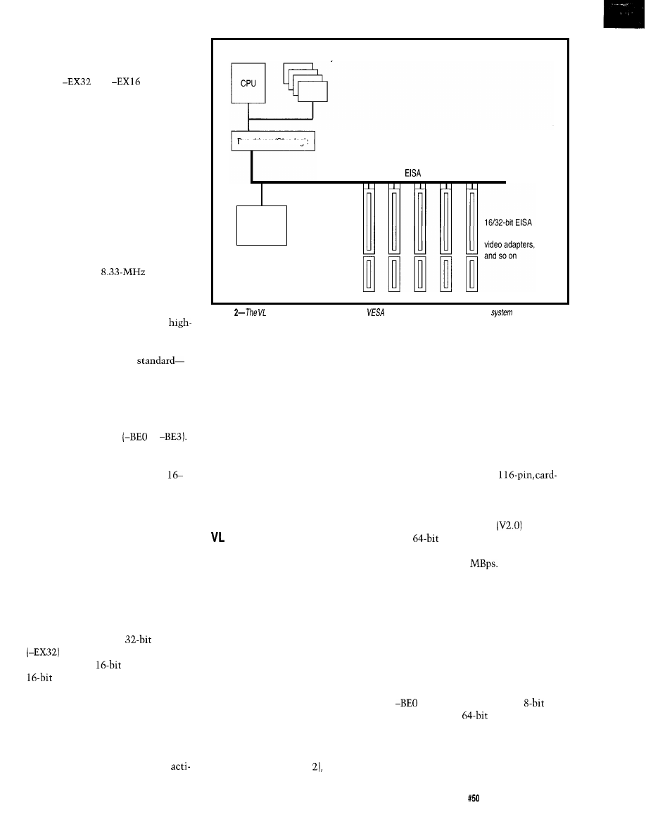
EISA switches automatically between
16-bit ISA and 32-bit EISA operation
using a second row of edge connectors
and the
and
lines. Thus,
EISA boards have access to all of the
signals available to ISA boards and the
second row of EISA signals.
As with the MCA bus, EISA sup-
ports arbitration for bus mastering and
automatic board configuration which
simplifies the installation of new
boards. The EISA bus can access fif-
teen interrupt levels and seven DMA
channels. To maintain backward com-
patibility with ISA expansion boards,
however, there is no direct bus support
for video or audio as there is with the
MCA bus. Since the EISA bus clock
runs at the same
rate as ISA,
the potential data throughput of an
EISA board is roughly twice that of ISA
boards. EISA systems are used as net-
work servers, workstations, and
end PCs. Although EISA systems have
proliferated more than MCA systems,
EISA remains a high-end
never really filtering down to low-cost
consumer systems.
The EISA bus uses 30 address lines
(Addr. 2-Addr. 31). The lower two
address lines (AO, Al) are decoded by
the Byte Enable lines
to
Data bits O-15 are taken from the ISA
portion of the bus, but the upper 16
data lines are provided by (Data
Data 31). Like the MCA, the M/-I/O
signal determines whether a memory
or I/O bus cycle is executed, while the
Write or Read (W/-R) line defines
whether the access is for reading or
writing. When an EISA device com-
pletes a bus cycle, the EISA Ready
(EXRDY) line is used to insert wait
states. When the motherboard is pro-
viding exclusive access to the EISA
board, the Locked Cycle (-LOCK) sig-
nal is true. If an EISA board can run in
32-bit mode, the EISA
Device
signal is true. But if the board
can only run in
mode, the EISA
Device (-EX16) signal is true.
The Master Burst (-MSBURST)
signal is activated by the EISA bus
master which informs the EISA bus
controller that a burst transfer cycle
will commence, thereby doubling the
bus transfer rate. When an external
device must send a data burst, it
Memorv
Bus drivers/Glue logic
Bus
Keyboard
bus slots for disks,
Figure
(Video Local) bus designed by
is local to the microprocessor and
memory and is
designed to allow the processor high-speed access to graphics and video electronics.
vates
the Slave Burst (-SLBURST) line.
An external device requests control of
the EISA bus using the Master Request
(-MREQ) line. If the bus arbitrator
decides that the requester can control
the bus, a Master Acknowledge
(-MACK) signal is sent to the request-
ing device. A Command (-CMD) signal
is sent to synchronize the EISA bus
cycle with the system clock, and the
Start (-START) signal coordinates the
system clock with the beginning of the
EISA bus cycle. Finally, the Bus Clock
(BCLK) is provided at 8.33 MHz.
The demands of data transfer
across the expansion bus have contin-
ued to evolve faster than the through-
put of classical ISA/EISA bus architec-
tures. The volumes of data required by
graphic user interfaces, such as
Microsoft Windows, presented serious
challenges to video adapter and
memory design. Early in 1992, the
Video Electronics Standards Associa-
tion (VESA) proposed a new local bus
standard called the Video Local (VL)
bus which was intended to improve
the performance of graphics and video
systems. In general terms, a VL bus is
a pathway that gives peripherals access
to the system’s main memory quickly.
For the VL bus (Figure such im-
proved access means higher data
throughput and performance for video
information at the speed of the CPU
itself. By using a stand-alone bus for
video, ISA or EISA buses can be imple-
mented for backward system compat-
ibility. Users can upgrade to a new
motherboard and graphics card, but all
other peripherals and software remain
compatible.
The VL bus uses a
edge connector with small contacts
(similar in appearance to Micro Chan-
nel contacts) as shown in Table 6. The
current VL bus release
offers a
full
data path (Data O-Data 63)
with a maximum rated data through-
put of about 260
The Data or
Command (D/-C) signal tells whether
information on the bus is data or a
command. Clock signals from the
CPU are provided through the Local
Bus Clock (LCLK) line. Memory or I/O
(M/-I/O) distinguishes between
memory and I/O accesses, while the
Write or Read (W/-R) signal differenti-
ates between read and write opera-
tions. Since the VL bus is 64 bits wide,
to -BE7 indicate which
portions of the
bus are being
transferred. A Reset signal (-RESET)
initializes the VL device, and the
Ready Return (-RDYRTN) line indi-
cates that the VL bus is accessible.
The Computer Applications Journal
Issue
September 1994
4 9
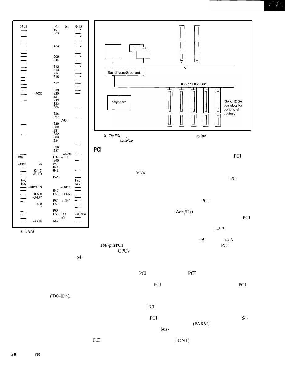
32 bit Pin
32
Data00 A01
Data 01
Data 02 A02
Data03
Data 04 A03
B03
Ground
Data06 A04
B04
Data05
Data08 A05
B05
Data 07
Ground A06
Data09
Data 10 A07
B07
Data 11
Data 12 A08
B08
Data 13
+VCC A09
Data 15
Data 14 Al0
Ground
Data 16 All
B l l
Data 17
D a t a 1 8 A l 2
+VCC
D a t a 2 0 A l 3
Data19
Ground Al4
Data21
Data 22 Al5
Data 23
D a t a 2 4 A l 6
B16
Data 25
D a t a 2 6 A l 7
Ground
Data 28 Al8
B18
Data27
D a t a 3 0 A l 9
Data29
A 2 0
Data31
Data 63
Addr. 31 A21
Addr. 30
Data62
Ground A22
Addr. 28
Data 60
Data 61
Addr. 29 A23
Addr 26
Data 58
Data 59
Addr. 27 A24
Ground
Data 57
Addr. 25 A25
B25
Addr. 24
Data 56
Data 55
Addr. 23 A26
Addr. 22
Data54
Data 53
Addr. 21 A27
+VCC
Data 51
Addr. 19 A28
B28
20
Data52
Ground A29
Addr. 18
Data 50
Data 49
Addr. 17 A30
Addr. 16
Data48
Data 47
Addr. 15 A31
Addr. 14
Data46
+VCC A32
Addr. 12
Data 44
Data 45
Addr. 13 A33
Addr. 10
Data42
Data 43
Addr. 11 A34
Addr. 8
Data 40
Data 41
Addr. 9 A35
B35
Ground
Data 39
Addr. 7 A36
Addr. 6
Data 38
Data 37
Addr. 5 A37
Addr. 4
Data 36
Ground A38
B38
35
Addr. 3 A39
-BE 4
Data 34
Addr. 2 A40
+VCC
A 4 1
-BE 1
-BE 5
-RESET A42
- B E 2
-BE 6
A 4 3
Ground
A 4 4
B44
-BE 3
-BE 7
W I - R A 4 5
-ADS
Key Key
Key Key
Key Key
Key Key
A 4 8
B48
Ground A49
-LDEV
A 5 0
A 5 1
B51
Ground
-BLAST A52
Data 32
A 5 3
+VCC
Data 33
ID A54
B54
I D 2
Ground A55
I D 3
LCLK A56
+VCC A57
B57
A 5 8
-LEADS
Table
bus (V2.0) was designed specifically
for graphics and video use.
Data bus width is determined by the
Local Bus Size
16 (-LBS16)
or Local
Bus Size 64 (-LBS64) signals. If a
bit bus width is used, the Acknowl-
edge 64-bit (-ACK64) signal is true.
In mid-1992, Intel Corporation
and a comprehensive consortium of
manufacturers introduced the Periph-
eral Component Interconnect (PCI)
bus. The VL bus was designed specifi-
cally to enhance PC video systems, but
the
bus (Figure 3) looks to
the future of
[and PCs in gen-
eral) by providing a bus architecture
that also supports peripherals such as
hard drives, networks, and so on.
Accessing the VL bus is a process
Unlike the VL bus,
uses an
of arbitration-much like the arbitra-
independent, internal clock frequency
tion that takes place on an MCA or
of 33 MHz. This decouples the
EISA bus. Each VL device is defined by
expansion device from CPU speed,
its own ID number
The
making it possible to upgrade future
Local Bus Ready (-LRDY), Local Bus
boards regardless of PC performance.
Device (-LDEV), Local Bus Request
With a 64-bit data path, the
bus
(-LREQ), and Local Bus Grant
(shown in Table 7) offers about the
(-LGNT) lines negotiate control of the
same data throughput as VL.
also
VL bus. In most cases, there is only
supports up to 16 slots (or expansion
one VL device on the bus, but arbitra-
devices) on the motherboard using
tion must be performed to ensure
mastering techniques, although only
proper access to memory.
video adapters will be available in
CPU
M e m o r y
VL
bus slot(s) for a
h i g h - p e r f o r m a n c e
v i d e o a d a p t e r
Bus
Figure
(Peripheral Component Interconnect) bus was designed
and a consortium of computer
manufacturers as a
system bus of the future.
Despite advantages offered by the
VL bus, there are some serious limita-
tions that must be overcome. Perhaps
most important is the
dependence
on CPU speed (fast computers must
use wait states with the VL bus) and
support of only 1 or 2 slots. As well,
the VL standard is voluntary; not all
manufacturers adhere to VESA specifi-
cations completely.
the immediate future. While systems
are now being developed with
compatibility, ISA or EISA buses are
also included to ensure backward com-
patibility. Given the tenacious history
of ISA buses, it is likely that
de-
vices will continue to share real estate
with ISA devices into the next decade.
To reduce the number of pins
needed in the
bus, data and ad-
dress lines are multiplexed together
0-Adr./Dat 63). From Table
7, it is also interesting to note that
is the first bus standard designed to
support low-voltage
VDC) logic
implementation. On inspection, you
will see that VDC and
VDC
implementations of the
bus place
their physical key slots in different
locations so that the two implementa-
tions are not interchangeable. The
Clock (CLOCK) signal provides timing
for the
bus only, and can be ad-
justed from DC to 33 MHz. Asserting
the Reset (-RST) signal resets all
devices. Since the 64-bit data path uses
eight bytes, the Command or Byte
Enable signals (C/-BEO-C/-BE7) define
which bytes are transferred. Parity
across the Adr/Dat and BE lines is
represented with a Parity (PAR) or
bit Parity
signal. Bus master-
ing is initiated by the -REQ line and
granted after approval using the Grant
line.
Issue
September 1994
The Computer Applications Journal
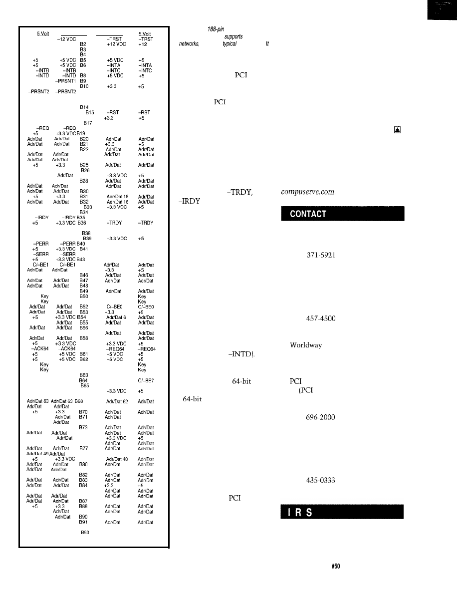
3.3 Volt
P
i
n
3 . 3 V o l t
Pin
-12 VDC
B l
A l
TCK
T C K
A 2
VDC
Ground
G r o u n d
A 3 T M S
TMS
TDO
T D O
A4 TDI
TDI
VDC
A 5
VDC
VDC
A 6
B 7
A 7
A 6
VDC
-PRSNTl
A9 Reserved
Reserved
Reserved
Reserved
A l 0
VDC (l/O)
VDC
B l l
Al 1 Reserved
Reserved
Ground
Key B12
A l 2 K e y
Ground
Ground
Key B13
A l 3 K e y
Ground
Reserved
Reserved
Al 4 Reserved
Reserved
Ground
G r o u n d
A l 5
Clock
Clock B16
Al6
V D C
VDC
Ground
G r o u n d
A l 7 - G N T
- G N T
B 1 6 A l 8 G r o u n d
Ground
VDC
A l 9 R e s e r v e d
Reserved
31
31
A20
30
30
2 9
2 9
A21
VDC
VDC
Ground
G r o u n d
A22
28
28
27
2 7 B 2 3 A 2 3
2 6
26
25
25 B24
A24 Ground
Ground
VDC
VDC
A25
24
24
C/-BE3
C / - B E 3
A 2 6 I D S E L
IDSEL
A d r i D a t 2 3
23 B27 A27
VDC
Ground
G r o u n d
A28
22
22
21
21 B29
A29
20
20
1 9
1 9
A30 Ground
Ground
VDC
VDC
A 3 1
18
1 7
1 7
A 3 2
16
C/-BE2
C / - B E 2
A 3 3
VDC
Ground
G r o u n d
A34 -FRAME
-FRAME
A 3 5 G r o u n d
Ground
VDC
A 3 6
-DEVSEL
-DEVSEL B37 A37 Ground
Ground
Ground
G r o u n d
A 3 8 - S T O P
-STOP
-LOCK
- L O C K
A 3 9
VDC
A 4 0 S D O N E
SDONE
VDC
A 4 1 - S B O
-SBO
B 4 2 A 4 2 G r o u n d
Ground
VDC
A 4 3 P A R
PAR
B 4 4 A 4 4
1 5
15
14
14 B45
A45
VDC
VDC
Ground
G r o u n d
A46
13
13
1 2
1 2
A47
11
11
10
10
A46 Ground
Ground
Ground
G r o u n d
A 4 9
9
9
G r o u n d
A50 Ground
Ground B51
A51 Ground
8
8
A 5 2
7
7
A53
VDC
VDC
VDC
A 5 4
6
AdriDat 5
5
A55
4
4
3
3
A56 Ground
Ground
Ground
Ground B57
A57
2
2
1
1
A58 AdriDat 0
0
VDC
B 5 9 A 5 9
VDC
B 6 0 A 6 0
VDC
A 6 1
VDC
VDC
A 6 2
VDC
Key Key
Key Key
Key Key
Key Key
Reserved
Reserved
A63 Ground
Ground
Ground
G r o u n d
A64 C/-BE7
C/-BE6
C / - B E 6
A 6 5 C / - B E 5
C/-BE5
C/-BE4
C / - B E 4 B 6 6 A 6 6
VDC
Ground
Ground B67 A67 PAR64
PAR64
A 6 8
62
61
61 B69
A69 Ground
Ground
VDC
VDC
A70
60
60
AdriDat 59
59
A71
58
AdriDat 56
AdriDat 57
57 B72
A72 Ground
Ground
Ground
G r o u n d
A73
56
56
55
55 B74
A74
54
54
A d r i D a t 5 3
53 B75 A75
VDC
Ground
Ground B76
A76
52
52
5 1
5 1
A77
50
50
4 9 B 7 8 A 7 6 G r o u n d
Ground
VDC
B 7 9 A 7 9
48
4 7
4 7
A80
46
46
45
45 B81
A81 Ground
Ground
Ground
G r o u n d
A82
44
44
4 3
4 3
A83
42
42
41
41
A84
VDC
VDC
Ground
Ground B85
A85
40
40
39
39 B86
A86
38
38
3 7
3 7
A87 Ground
Ground
VDC
VDC
A88
36
36
AdriDat 35
35 B89
A89
34
34
AdriDat 33
33
A90 Ground
Ground
Ground
G r o u n d
A91
32
32
Reserved
Reserved B92 A92 Reserved
Reserved
Reserved
R e s e r v e d
A93 Ground
Ground
Ground
Ground B94
A94 Reserved
Reserved
Table 7-The
PC/ bus provides
a
bus architecture that
hard drives,
and other
peripherals.
also
handles both 5-V and 3.3-V system
power.
When a valid
bus
cycle is in progress, the
Frame (-FRAME] signal is
true. If the
bus cycle is in
its final phase, Frame will be
released. The Target Ready
(-TRDY) line is true when an
addressed device is able to
complete the data phase of its
bus cycle. An Initiator Ready
(-IRDY) signal indicates valid
data is present on the bus or
the bus is ready to accept
data. -FRAME,
and
are used together. A
Stop (-STOP) signal is as-
serted by a target asking a
master to halt the current
data transfer. ID Select
(IDSEL) is used as a chip se-
lect signal during board con-
figuration. Device Select
(-DEVSEL) is both an input
and an output. As an input, it
indicates if a device has as-
sumed control of the current
bus transfer. As an output, it
shows that a device has iden-
tified itself as the target for
current bus transfer.
There are four interrupt
lines (-INTA to
When the full 64-bit data
mode is used, an expansion
device initiates a
Bus
Request (-REQ 64) and awaits
a
Bus Acknowledge
(-ACK64) signal from the bus
controller. The Bus Lock
(-LOCK) signal is an interface
control used to ensure use of
the bus by a selected expan-
sion device. Error reporting is
performed by Primary Error
(-PERR) and Secondary Error
(-SERR) lines. Cache memory
and JTAG support are also
provided on the
bus.
CONCLUSION
Through standardized
bus interfaces, computers can
work with peripheral prod-
ucts made by any number of manufac-
turers. Such open architectures have
contributed to the inexpensive, readily
available computers that we have
today. In the last decade, bus architec-
tures have come a long way. As they
continue to change to keep pace with
the advances in computer technology,
an understanding of past and present
bus structures helps you make the
most of your current systems as well
as preparing you for future changes.
Stephen Bigelow is an electrical
engineer working as a technical editor
and writer at Dynamic Learning
Systems. He may be reached at (508)
366-9487 or at 73652.320%
BCPR Services (EISA Specifications)
1400 L Street, NW
Washington, DC 20005
(202)
Electronic Industries Association
(EIA)
Engineering Department
2001 Eye Street NW
Washington, DC 20006
(202)
IEEE Computer Society Press
Postal Center
Los Angeles, CA 90080
(714) 8218380
Special Interest Group
SIG)
P.O. Box 14070
Portland, OR 97214
(503)
Fax: (503) 693-0920
Video Electronic Standards
Association (VESA)
2150 North First St., Suite 440
San Jose, CA 95 13 l-2029
(408)
Fax: (408) 435-8225
413
Very Useful
414 Moderately Useful
415 Not Useful
The Computer Applications Journal
Issue
September 1994
51
DEPARTMENTS
Firmware Furnace
From the Bench
Silicon Update
Embedded Techniques
Ed Nisley
Journey to the Protected Land:
Smashing Bugs in Gates
n real-mode PC
programming, it’s
branches will corrupt data, code, stack,
or heap space somewhere in that first
megabyte of RAM. Protected mode
doesn’t solve those problems, but it’s a
lot easier to find the problems when
the CPU says
this pointer
looks bogus” or “Umm, you don’t
really
want to execute this data, do
you!”
Now that our code is running in
protected mode, it’s time to
check out the scenery. This month, I’ll
cover branches and calls, describe how
call and interrupt gates are applied in
the IDT, then check out some inter-
rupt-handler response times.
We are now venturing into the
complex
part of this Complex-Instruc-
tion-Set CPU. In real mode, the CPU
does fairly simple things that don’t
take too long. In protected mode,
there’s a lot going on under the covers.
Stay alert!
‘JMPING’ AND CALLING
Real-mode 386 programs branch
hither and yon using J M P, CALL, and
I NT instructions with hardware
interrupts sharing much of the I NT
machinery. All this remains true in
protected mode, but, as you’ll see, we
52
Issue
September 1994
The Computer Applications Journal
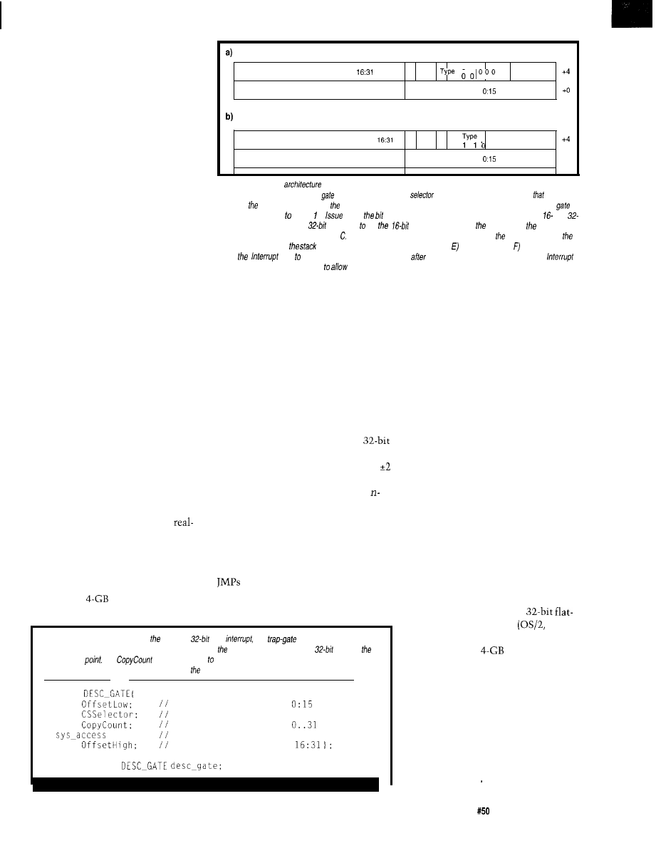
have several other choices that not
only simplify branching, but help keep
bugs under control. First, the basics..
The distinction between N EAR and
FAR jump instructions is familiar to
anyone with 80x86 programming
experience. Simply put, N EAR J M Ps
don’t change the CS register. FAR J M Ps
transfer control to a different code
segment, loading CS with the new
segment address in the process. Both
types load the IP (Instruction Pointer)
register with the offset of the target
instruction.
CA L L instructions save the address
of the next sequential instruction on
the stack before branching to the
target instruction. A N EAR CA L L
pushes only the offset of the next
instruction, while a FAR CALL first
pushes the CS register.
The whole purpose of a CA L L is to
invoke a routine that will eventually
return to the instruction after the
CALL. RET instructions come in NEAR
and FAR flavors that must match the
CALL, although there is no way to tell
how you got to a particular routine.
Thus, it’s essentially impossible to
write a routine that’s N EAR to some
callers and FAR to others.
Pairing a FAR CALL with a NEAR
RET leaves the caller’s CS on the stack.
Conversely, mismatching a NEAR CALL
with a FAR RET restores something to
CS. In either case, the CPU returns to
the wrong address. Finding this
problem is a favorite pastime of
mode programmers.
The 8086 required FAR branches
because real-mode code segments were
limited to 64 KB. That restriction
simply Goes Away in 32-bit PM; you
can define a
code segment if you
like. Most application programs won’t
3130292827262524232221201918171615~413121110 9 8 7 6 5 4 3 2 1 0
offset
P DPL 0
Count
, ,
Code Segment Selector
offset
31302928272625242322212019181716151413121110 9 8 7 6 5 4 3 2 1 0
Offset
PDPLO
00000000
,
Code Segment Selector
Offset
+o
Figure l--The 80386
encourages control transfers through gates, which are special system segment
descriptors. The address fields in a
descriptor contain a code
and an offset address within
code
segment; layout is different from usual memory and system segment descriptors. This diagram shows
field definitions; refer Figure in
48 for definitions. For 80286 compatibility, there are a/so and
bit gates: subtract 8 from fhe
Type field gef
Type and make sure high word of address
offset field is zero. a) Call gate, Type = The Count field is not used when fhe caller has
same privilege as
called routine because
entries are nof copied. b) Interrupt (Type = and trap (Type = gates. The CPU
clears
Flag prevenf further hardware interrupts
passing through an Interrupt gate. The
Nag is not changed by trap gates
hardware interrupts in trap handlers
need FAR branches to reach their own
routines.
Mismatched CAL L/RET pairs
generate a protection exception when
CS is reloaded with junk from the
stack or when the CPU executes an
invalid instruction after returning to a
bad address. The error handler can
show you the exact location of the
error, which is certainly better than
having your system quietly lock up or
hose the screen with pinball panic.
Another irritant vanishes in
PM; conditional J M P instructions can
now reach a target anywhere within
GB. The 8086 limitation of t128 bytes
spawned an arms race resulting in
pass optimizing assemblers (!) that
shuffle your code around to find the
smallest, fastest combination of J M Ps
to
reach the target instruction. No
more of that!
Admittedly, the new conditional
are six-byte behemoths instead
of the svelte two-byte instructions
you’re used to. Those optimizers will
Listing l--This structure contains fields for
call,
and
descriptors. Unlike
ordinary memory and system descriptors, gates include code-segment selector and
offset of
routine entry
The
field applies on/y call gafes fhaf transfer control between different
privilege /eve/s, which We aren’t concerned about for time being.
struct
WORD
routine offset address
WORD
routine CS selector
BYTE
stack entries to copy,
Access;
access bits
WORD
routine offset address
typedef struct
figure out what you really wanted to
code if you let them, although, as
you’ll see, there are some situations
where such optimization is precisely
what we don’t want.
Even if all your application’s code
is in one segment, you still need a way
to communicate with the operating
system. Direct branch-into-the-OS
interfaces are ancient history, so it
should be no surprise that the ‘386 has
a cleaner method. In grand CISC style,
there are actually several ways to
accomplish the goal.
Quiz: Which major IBM main-
frame program branched directly into
the operating system to improve
performance?
Extra credit: What effect did that
have on future operating system
enhancements?
GATES IN THE WALL
Once the restrictions of real-mode
addressing go away, you can do lots of
interesting things. Current
model operating systems
Windows NT, and suchlike) use the
vast expanse of a
address space to
good advantage. The entire application
fits neatly into the first 2 GB, while
the operating system is tucked into the
upper 2 GB.
Does anyone yet remember when
64 KB was enough for the operating
system and the application? It wasn’t
that
long ago when 1 MB (well, 640
KB) was enough. Surely 2 GB ought to
last for a while..
The Computer Applications Journal
Issue
September 1994
5 3
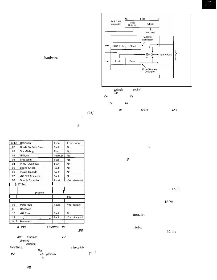
Just like IBM’s ATF (which, as I
recall, mutated into TPF with those
branch targets agonizingly intact) it
seems you can once again J M P right
into the operating system!
The ‘386 (and ‘486 and Pentium)
protection hardware prevents that by
running the application at a low
privilege level and forbidding access to
the more-privileged OS code. In any
event, it’s a Bad Idea to
somebody else’s addresses into your
instructions.. that’s obvious by now,
isn’t it?
software, while
interrupt and trap
gates are used in
the IDT to pass
control to inter-
rupt and error
handlers. Task
gates will become
vitally important
when we begin
using the 80386
multitasking
hardware.
Figure 1
shows the fields
within call,
interrupt, and trap
gates. The address
fields are slightly
different from the
memory and
system segment
descriptors
I
showed in
48,
but the and DPL
The 80x86 architecture encour-
ages a different method: passing
control through a gate. Just as a
barnyard gate restricts the flow of
cattle, a programming gate restricts a
program’s flow of control. An applica-
tion can invoke an operating system
function through a gate without
knowing the function’s address, so the
OS can change without affecting the
application program at all.
GDT or LDT
Figure 2-A
transfers
to a function in a new code segment using two
descriptors.
process starts with a FAR CA L L containing a selector corresponding
to call gate’s descriptor; four-byfe offset in the CA L L instruction is ignored. The
call gate descriptor contains the new code segment’s selector and the entry point
offset.
CPU loads new code segment descriptor, adds the call gate’s offset
field to the segment base address, and branches to the function. The process is much
more complex if programs use the
privilege hardware, but
ignore that
for now.
Gates fall into four main catego-
bits serve the same functions. All of
ries: call, interrupt, trap, and task. Call
our bits will be set to indicate that
gates correspond to ordinary function
the segments are present, and we run
CAL Ls in application or system
with DPL=O to gain maximum
Code
Segment
Memory
won’t use this feature, but it’s the sort
of thing you can do if you feel the
need. Talk about a simple matter of
programming..
Listing 1 is the C structure that
defines the fields within gates. The
C
o
py
C o
n t
field is used only in call
gates between code of different
privilege levels; it holds the number of
stack entries to copy between the
stacks at each level. Fortunately,
because we are running at the highest
privilege level, we don’t have to worry
about that nuance just yet, but we’ll
get into it eventually.
For compatibility with older
80286 code, there are also
versions of these gates formed by
subtracting 8 from the Type field.
These gates push the
IP rather
than all 32 bits of EIP onto the stack.
So, if the high-order bits of EIP were
when the gate is invoked, a
RET can’t take you home again! The
error handling code this month uses
gates, but will likely be the last
time you see them in a
program.
Call gate descriptors must be
located in the GDT or LDT while
interrupt and trap gate descriptors
must be in the IDT. Invoking a call
gate is a simple matter of executing a
FAR CALL or JMP with the gate’s
privilege.
Gates provide so
much isolation that the
function need not even be
present in RAM when the
application calls it. If the
bit is zero, the CPU
invokes the “segment not
present” handler when the
application uses the gate.
The error handler figures
out which segment caused
the error, determines
which disk file contains
the code corresponding to
that gate, reads it into
RAM (perhaps swapping
another segment out in its
place), marks the gate
“present,” aims it at the
code, then reexecutes the
CAL L. This time it will
work normally, so the
application doesn’t know
anything out of the
ordinary happened!
Complex enough for
The Firmware
Furnace Task Switcher
09
O v e r r u n
Abort No
OA Invalid TSS
OB Seament not
Fault
Yes
Fault Yes
OC Stack fault
Fault
I
OD
General protection
Fault
Yes
Alignment check (486 only)
Figure
reserves the first 32
for CPU hardware.
About ha/f remain unused, but we’// not make the same mistake as
did in the Original PC; as far as we’re concerned, “reserved” means
“hands
The
between Faults, Traps,
Aborts is simple:
faults are
before the instruction is complete, Traps occur after
the instruction is
and Aborts are catastrophic failures. The
is a special case that is recognized at the next
point between instructions.
CPU pushes an error code on the stack
if error can be associated
a
segmenf or value; the
error handler can use the code track down and resolve the problem.
5 4
Issue
September 1994
The Computer Applications Journal
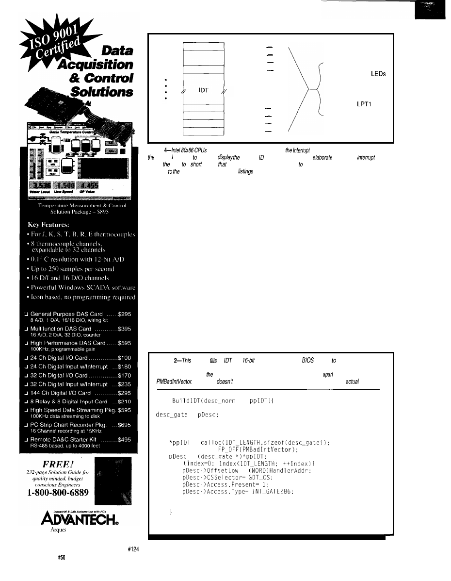
Int FF
Int FE
Int FD
Int FC
Int 03
Int 02
Int 01
Int 00
PUSH OOFF
JMP
PUSH OOFE
JMP
PUSH OOFD
JMP
PUSH OOFC
JMP
POP ID
Display on FDB
POP error code
Display on LPT2
POP IP
PUSH 0003
JMP
PUSH 0002
JMP
PUSH 0001
JMP
PUSH 0000
JMP
Display on
Stall
Figure
invoke interrupt handlers through
Descriptor Table. This diagram sketches
method used save and
interrupt number without a lot of
code. Each
gate
directs CPU a
routine
pushes a constant corresponding the interrupt ID number and fhen
branches common error routine. The
in this column show the code required for each piece of this
puzzle.
selector as part of the branch
address. Trap and interrupt gates are
invoked by one of the I NT instruc-
tions, all hardware interrupts, and any
of the CPU error detectors.
Figure 2 shows how a call gate
works. The CPU uses the FAR CAL L's
selector to locate the call gate in the
GDT or LDT. That descriptor contains
the code segment selector and offset
for the function, along with several
other fields. Fetching and loading all
the descriptors is a fairly lengthy
process, so passing through a call gate
can take 50-100 cycles rather than the
ten you’re used to in real mode.
The return process is somewhat
simpler. When the CPU encounters a
RET instruction, it pops the selector
and offset of the return address from
the stack and transfers control back to
that code segment. As long as you’re
not passing from one privilege level to
another, RET isn’t much more expen-
sive than in real mode.
Because our code is running at the
highest privilege level, the CPU does
not invoke the checks needed to verify
transfers between privilege levels.
Eventually we must know about that
machinery, but for now I’m keeping it
simple.
Honest, this
is
the simple version!
Interrupt and trap gates are similar
to FAR CA L Ls except that the gate is
identified by an interrupt number,
Listing
function an
with
interrupt gates for the
“Switch Protected Mode”
function. Each
gate transfers control to one of the small routines that pushes the interrupt ID on the stack
and branches to common handler. Those routines are spaced eight byfes
starting at
This listing
include the error checking and display routines in the
code.
int
**
*
int Index;
LADDR HandlerAddr;
=
HandlerAddr =
=
for
=
++pDesc;
HandlerAddr += 8;
return 0;
750 East
Ave., Sunnyvale, CA 94086
Tel: (408) 245-6678 FAX: (408) 245.8268
56
Issue
September 1994
The Computer Applications Journal
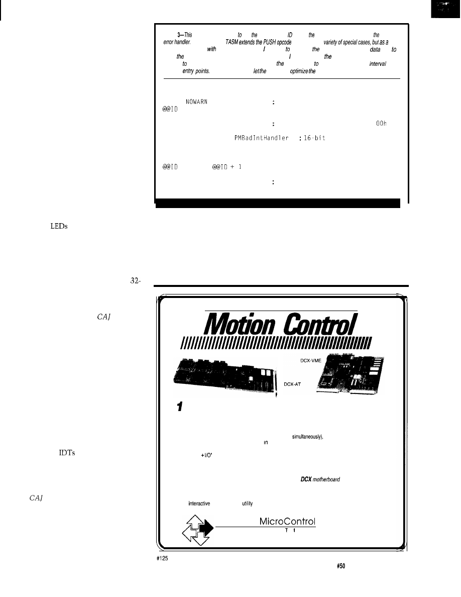
rather than a selector in an instruction
(so the descriptor must be in the IDT),
and the CPU pushes the Flags register
on the stack before saving CS and IP.
The interrupt may be caused by an
I NT instruction, an external hardware
interrupt, or a CPU error condition.
Once the gate is activated, the same
actions shown in Figure 2 take place.
The interrupt handler must return
using an I RET instruction to restore
the Flags register. As in real mode, if
you RET instead of I RET, things go
awry in a hurry. Fortunately, the CPU
will detect the problem and tell you
what happened.
Probably the best way to see how
all this works is to watch some code in
action. At this point we don’t have
much of an operating system, so I’ll
exercise a pair of interrupt gates using
hardware interrupts. Once again, a few
blinking
will either confirm that
the code is running correctly or help
diagnose the problem.
First, we will review the 16-bit
interrupt handlers that are already in
place to capture CPU errors. Then I’ll
aim two of the IDT entries at new
bit handlers and make a few response
time measurements. If you’re just
getting up to speed with real-mode
interrupts, refer back to
35 where
I covered the grisly hardware details of
your PC’s interrupt system.
ERROR CENTRAL
The Interrupt Descriptor Table
defines all of the interrupt handlers
available to the CPU. Just as in real
mode you may have up to 256 han-
dlers, but now you can safely provide
only the actual number of handlers
you need because the CPU will trap
any attempt to invoke a handler “off
the end” of the IDT. You can also put
the IDT at any convenient location
and change
by simply reloading
the CPU’s IDT Register.
Figure 3 shows the 32 interrupts
reserved for CPU-detected errors. This
figure is similar to one that appeared
in
35, but we no longer have to
worry about real-mode BIOS functions
and hardware interrupts colliding with
the Intel reserved interrupts. Those
interrupts should invoke a “Can’t
Happen Here” handler, but they ought
Listing
code creates 256 routines push interrupt onto stack and branch to common
Borland's
fo handle a
result it has trouble
this simple situation. resorted encoding PUSH instruction as a
byfe
avoid extended functions; there may be a beffer way. also turned off “Inefficient Code Generation”
warning avoid spurious messages resulting from code needed maintain an eight-byte
between
Be sure you don’t assembler
NOP instructions ouf of existence!
PROC
PMBadIntVector
PUBLIC PMBadIntVector
ICG
suppress inefficient code warning
=
0
REPT
256
DB
06Ah
PUSH immediate byte, MSB =
DB
@ I D
JMP
SMALL
offset
NOP
NOP
NOP
=
ENDM
WARN
ICG
resume warnings
ENDP
PMBadIntVector
not be used for any other system
covering the IDT so it can load the
functions.
IDTR correctly. That data segment
Because an error may occur at any
descriptor gives the starting address
time, the IDT must be valid when the
and length of the segment, which is
CPU enters PM. The BIOS “Switch to
what the LIDT instruction requires.
Protected Mode” requires a read/write
The BIOS disables external
data descriptor for GDT selector 0010
interrupts before switching modes, so I
Multi-Axis
to 8 Axis Motor/Motion Controllers
l
DCXcontrollers incorporate state-of-the-art DSP, RISC; and FPGA technologies to insure
maximum performance at minimum cost
l
DCXcontrollers provide many sophisticated ON-BOARD control features such a MULTI-
TASKING (the ability to perform independent tasks
COMPLEX-CONTOURING,
and the ability to programmed directly USER-UNITS such as inches, meters, etc.
l
DCXcontrollers can operate totally STAND-ALONE, using their own on-board “computing +
memory
capabilities, or EMBEDDED in a machine. They can also be installed in an
ISA-bus (PC/XT/AT), or in a VME-bus (6U)
l
DCXcontrollers have a MODULAR ARCHITECTURE for creating a limitless variety of
Application Specific MULTI-AXIS controllers. They are created, in minutes. by installing one or
more intelligent
DCX function modules
on an intelligent
l
DCXcontrollers are supplied with (free) EASY-TO-USE, POWERFUL SOFTWARE for set-
up, programming and operating. These include all major HLL interface programs, with
examples and source code, a CNC control user-interface with G-code and HPGL capability, and
an
Servo-Tuning
Precision
TEL (619) 565-1500
C
0
R
P
0
R
A
0
N
8122
Engineer Rd.
l
San Diego, CA 92111
FAX (619) 565-l 511
The Computer Applications Journal
Issue
September 1994
5 7
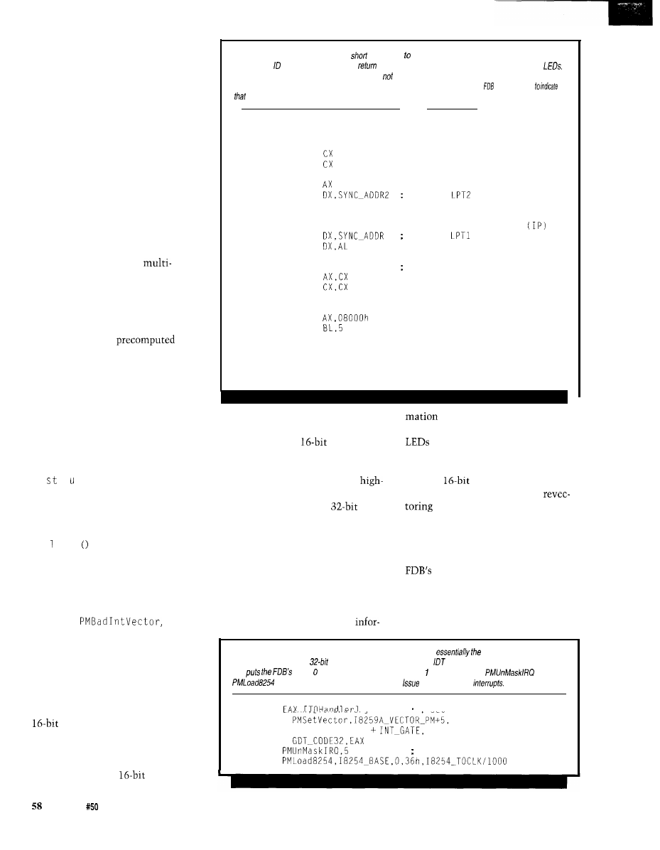
filled all 256 IDT entries with 16-bit
gates leading to a single-error handler
that would take control if any inter-
rupt occurred, no matter what the
cause. The references describe the
differences between fault, trap, and
abort interrupts, but, for our present
purpose, they’re all the same. If any
interrupt occurs, it means the code
encountered a problem that we’ll have
to fix manually.
However, using a single interrupt
handler discards a key piece of infor-
mation-the interrupt ID that invoked
the handler. It’s a characteristic of the
Intel method of generating and
handling interrupts that an interrupt
selects its handler, but a
interrupt handler can’t identify who
invoked it.
Figure 4 sketches how I got around
this problem. Each interrupt gate is
aimed at a short chunk of revectoring
code that pushes a
constant corresponding to the inter-
rupt ID onto the stack, then branches
to the common handler. Popping the
constant from the stack provides a
quick and easy way to identify the
interrupt’s source, at the cost of an
intermediate layer of code that
occupies quite a bit of space.
Listing 2 shows the C code that
generates the gates in the IDT using
the
r
c t
layout shown in Listing 1.
This code executes in real mode so the
IDT is just another chunk of RAM
within the current data segment.
I
allocated it from the near heap using
c a
1 oc
to zero-fill all the unused
fields, then filled in the required
information.
The macro in Listing 3 generates
the revectoring routines. The 256
entry points occur every eight bytes
startingat
which
meant I needed tight control over the
generated code. After several attempts
to keep the assembler from helping
me, I finally defined
PUSH as a data
byte and specified the branch target as
a 16-bit
SMALL
value.
The interrupt code is located in a
code segment and must be
entered through a 16-bit interrupt gate.
Even if the error causing the interrupt
occurs in a 32-bit code segment the
CPU will switch to
mode before
Listing 4-An error handler should be
and simple ensure that it works correct/y. This code recovers
the interrupt number, error code, and
address from the stack and displays them on various
Obviously there is room for future improvemenf,
the least of which will be to handle the case where there
is no error code on the stack! The code blinks one of the decimal points on the LED digits
fhis routine is in control.
PROC
PMBadIntHandler
PUBLIC PMBadIntHandler
POP
NOT
POP
MOV
OUT
DX,AL
POP
MOV
OUT
AX
MOV
MOV
XOR
@Stall:
OUT
XOR
MOV
@@Punt:
LOOP
DEC
JNZ
JMP
ENDP
DX,LED_ADDR
DX,AX
@ P u n t
BL
@ P u n t
@Stall
PMBadIntHandler
recover the interrupt ID
flip it to make it readable
recover error code
show on
low byte only
recover return address
show on
. low byte only
set up for the display
recover interrupt ID
set up initial count
display new data
flip the high decimal point
delay for a decent interval
pushing anything on the stack. Thus,
from the stack and displays
the default data size is 16 bits and the
them in raw binary on the various
stack will contain
entries,
attached to the system. Later on
including the return address.
we’ll make it more attractive, but for
The
PUSH
instruction extends its
now it gets the job done.
immediate byte operand with a
The
value atop the stack is
order zero byte and pushes a complete
the Interrupt ID pushed by the
word onto the stack. In a
code
segment this instruction would extend
the byte with three zero bytes and
push a 32-bit value onto the stack. If
you mix code segment sizes, it can be
difficult to tell what’s on the stack.
Listing 4 presents the error
handler, which is an exercise in
brutally simple, user-hostile code. It
recovers several vital pieces of
routine. The code pops this into
CX for safekeeping while recovering
and displaying the remaining informa-
tion. The handler eventually enters a
spin loop that displays the ID on the
LED digits and blinks one of the
decimal points to indicate that it’s
stalled.
The next stack entry may be an
error code if the CPU generates one for
Listing B-Setting up a profecfed mode interrupt handler requires
same steps as in real
mode. This code loads a
interrupt gate into the appropriate
descriptor, resets the 8259 mask bit,
and
Timer into Mode 3 to produce a periodic ms inferrupt. The
and
routines are similar to the code shown in
35 for real mode
LEA
set up interrupt vector
C A L L
\
(MASK Present)
\
CALL
set up interrupt controller
CALL
Issue
September 1994
The Computer Applications Journal
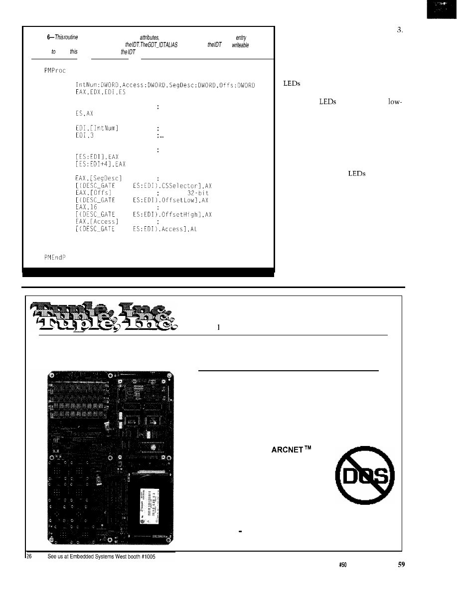
Listing
inserts an
interrupt gate’s
code segment selector, and
32-M
point
offset
address into
a
descriptor
in
selector
maps
as a
dafa
segment allow updafe; otherwise, is not
directly addressable.
PMSetVector
ARG
USES
MOV
EAX,GDT_IDTALIAS
get data access to IDT
MOV
MOV
get pointer to descriptor
SHL
eight bytes each
XOR
EAX,EAX
zero the entire descriptor
MOV
MOV
MOV
set code segment descriptor
MOV
PTR
MOV
set up
offset
MOV
PTR
SHR
align high word
MOV
PTR
MOV
set segment access bits
MOV
PTR
RET
PMSetVector
this interrupt, as indicated in Figure
Obviously, a more friendly handler
would decode the Interrupt ID and
either extract or skip the error code.
This handler simply pops a 16-bit
value and displays the low byte on the
connected to port 0278.
If the CPU didn’t push an error
code, these
will display the
order byte of the Instruction Pointer
rather than the error code. Given the
size of the code segment, this ought to
be enough to identify the failing
instruction, but some sleuthing may
be in order.
The low byte of the next stack
entry appears on the
at port
0378. If the CPU pushed an error code
this will be the Instruction Pointer;
otherwise, it’s the CS selector value.
This code will give you an idea of
what failed. In upcoming columns,
we’ll add more features to the error
handler and improve the displays so
they’re really useful. One of the
fundamental rules of building new
code is to not complexicate everything
at once!
18732 SE 43rd Street
Issaquah, WA 98027
WANTED:
206-746-3935 Voice
BETA SITE DEVELOPERS!
206-78 I-963
FAX
Are you tired of fighting with non-native development systems? Are you tired of circumventing non-real time
system software? Are you tired of trying to make your applications work on a PC? Are you tired of trying to
package your PC for factory floor applications? The Tuple Computer is just what you’re looking for!
l
Native development/ Target 68K system (68341)
l
ANSI ‘C’ Compiler, Linker, Loader, Debugger
l
200 MB Shock Tolerant Disk On Board
l
Graphics Co-Processor On Board (1024x768)
l
Up to 64 MB Ram
l
Four Serial Ports plus
l
Industrial Temp and Packaging
l
Real Time Pre-Emptive Scheduling
l
On Board Battery Backed RAM
l
8 X 11 inch Board Size
l
Expansion via Native 68K Bus
l
768Kb Flash On Board Programmable
The Computer Applications Journal
Issue September 1994
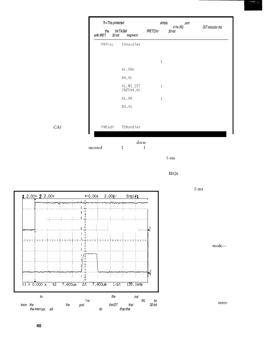
Now that we have the error
handler under control we’re ready to
try something new. With any luck
you’ll never see that blinking decimal
point....
STAND BY FOR INTERRUPTION!
The BIOS “Switch to protected
Mode” function requires a valid IDT
and the new Interrupt ID numbers
corresponding to the two 8259 Pro-
grammable Interrupt Controllers on
the system board. Recall that the first
8259 produces Int 08 through Int OF in
real mode, compare that to Figure 3,
and you’ll see why it must be changed.
The BIOS reprograms the 8259
Interrupt Vector Byte registers using
the new Interrupt ID bytes. I picked 50
and 70 (hex) because those are the two
more-or-less standard values. Refer
back to the column in
35 for more
details on how 8259s handle interrupt
inputs and interface to the CPU.
The BIOS also disables all external
interrupts by loading FF into the 8259
Listing
mode interrupt handler
blips a printer
bit and returns. The scope trace
in Photo 1 shows that about 7 ms elapse from the rising edge
line to the
turns on porf
3.1 requires an
force a
operation; Version 4.0 works correct/y
in a
code
PUSH
EAX
PUSH
EDX
MOV
EDX,SYNC_ADDR
send a trace output
IN
AL,DX
OR
OUT
DX,AL
MOV
MOV
send EOI to controller
OUT
MOV
clear trace output
AND
AL,NOT 08h
OUT
POP
EDX
POP
EAX
IRETD
Incidentally, this isn’t
The Firmware Development Board
anywhere could find; had to
has an 8254 that can produce an
Interrupt Mask Registers. This is
disassemble the BIOS code to make
obviously a last-ditch attempt to
sure it worked this way. Sometimes it
prevent unexpected interrupts in PM,
seems that all the references simply
but it seems to me that if you’ve gone
repeat each other, and you’ve got to
to the trouble of setting up an IDT,
actually try it out to get the straight
you’ll have valid interrupt handlers in
dope. But that’s what this column is
place.
all about, right?
STOP
. . . . . . .
,
. . . . . . . . . . . . . . . . . . . .
=
=
=
Photo l-Responding an interrupt fakes more time in protected mode, but difference may be as greaf as
interrupt on IRQ 5. I set Timer 0 up for
a
tick rate. If you haven’t built
the Graphic LCD interface you can
also experiment with Timers 1 and 2
on
10 and
15,
respectively. For
those of you who haven’t yet built any
hardware at all, I set up Timer 0 on the
system board for
interrupts on
IRQ 0.
Preparing a PM interrupt handler
should be familiar to anyone who’s
done real-mode programming. Listing
5 shows the sequence of events for the
FDB timer: capture the interrupt
vector, set up the hardware, then clear
the 8259’s IMR bit. That’s all there is
to it!
Listing 6 has the key difference
between real and protected
filling in an IDT entry, rather than
capturing a raw vector address. ES
holds the data selector alias for the
IDT that allows access to that chunk
ofRAM.IusedthePUSHFDandPOPFD
instructions to maintain 32-bit stack
alignment.
After all that setup, the interrupt
handler in Listing 7 is almost anticli-
mactic. It raises a bit in port 0378,
you think. In this case, a simple inferrupthandferdisplays a
response fime: the upper trace is the line,
lower
is handler's output on parallel
The interrupt gate in
ensures
fhe CPU is in
sends an EOI command to the
mode during
so register and stack operations default 32 bits rather
usual 16 bits found in
rupt controller, and clears the bit. The
real mode.
result is shown in photo l-the upper
60
Issue
September 1994
The Computer Applications Journal
trace is the rising edge of IRQ 5 on the
ISA bus, the lower trace is the printer
port trace bit. The overall delay is
about 7 us, which includes the time
required to save two
registers
and twiddle the port.
The fastest real-mode handler I
presented in
35 required 5 to
get to about the same point. Although
the PM code is slower, it’s not a lot
slower.. .and that may come as a
surprise. Yes, you can write PM code
that runs down on the bare metal in
the microsecond range.
Maybe this 32-bit protected mode
stuff isn’t such a bad idea after all?
Admittedly, this is about as
simple as an interrupt handler can get.
When we start switching tasks and
privilege levels, the response time will
drag out as the CPU does more work
on our behalf. We’ll keep those scope
probes ready to track the changes and
understand what’s going on.
RELEASE NOTES
The code this month checks out
two interrupt sources on your system.
If all goes well, you should see a pair of
dimly lit
on the
port
monitor box and a rapid count on the
Firmware Development Board’s LED
display. If there’s a problem, the FDB
will show you the trap ID number in
raw binary, and
will display the
error code.
Borland’s TASM 3.1 had a bug that
clobbered 32-bit constant calculations:
you could define a
constant, but
the arithmetic operators used only the
low-order 16 bits. Version 4.0 fixed
that, but it optimizes branches a little
more aggressively and is more strongly
typed, which broke some code.
Although it pains me to say this, you’ll
need the latest and greatest Borland
assembler to compile the code starting
with this month’s column. I will
continue using C++ 3.1 for the
mode code, though.
Shortly after last month’s column
went read-only, I got a flyer from Intel
saying that their databooks and
component manuals are now available
only from McGraw-Hill. Naturally,
McGraw-Hill changed all the order
numbers, so you’ll have to call (800)
822-8 158 for more information.
Thanks to Marshall, Lou, and Pete
in Hewlett-Packard’s Raleigh branch
office for showing off an
oscilloscope. They knew I couldn’t live
without one.. the scope “photos”
will be digital from now on.
Next month, we return to real
mode and the mysteries of the DOS
FAT file system to build a loader that
fetches a program from disk, stuffs it
into RAM, and fires it up in
protected mode.
q
Ed Nisley, as Nisley Micro Engineer-
ing, makes small computers do
amazing things. He’s also a member of
the Computer Applications
engineering staff. You may reach him
at
or
416
Very Useful
417 Moderately Useful
418 Not Useful
Memory mapped variables
In-line assembly language
option
Compile time switch to select
805
or
Compatible with any RAM
or ROM memory mapping
Runs up to 50 times faster than
the MCS BASIC-52 interpreter.
Includes Binary Technology’s
cross-assembler
hex file
n
Extensive documentation
n
Tutorial included
Runs on IBM-PC/XT or
n
Compatible with all 8051 variants
$295.
508-369-9556
FAX 508-369-9549
q
Binary Technology,
P.O. Box
l
Carlisle,
MA 01741
T
E
C
H
N
O
L
O
G
Y
The Computer Applications Journal
Issue
September 1994
6 1
Probing the
Dark Side:
the Motorist’s
Aid to
Hindsight
Jeff Bachiochi
heck the
mirrors, the coast
is clear, turn signal
on, accelerate, pull out,
and pass. We don’t think much about
this driving skill until someone cuts
us off or worse yet we cut someone off.
They (you) didn’t mean it; you [they)
were in their (your) blind spot.
An auto’s blind spots are located
in the lanes beside your car and run
from just behind your vehicle to the
position immediately adjacent to the
driver. The rear view mirror doesn’t
cover these areas, and the side mirrors
cover only a small section of them.
Convex mirrors, which either clip onto
the rear view or stick onto the side
mirrors, give the driver a wider field of
view, but they also distort distance.
And, if you ride a motorcycle you’re
stuck with just side mirrors.
One solution to this problem
might be to never drive without a
copilot. The copilot’s job would be to
ride backwards, thereby gaining an
unobstructed view of oncoming traffic.
This, of course, would cause many
communication problems: “Car fast
approaching on right. Swerve left..
My left-not yours.” And, although
permissible in an auto, most patrol
officers would frown on seeing
motorcyclists riding back-to-back.
I find myself riding my
Shadow to work more often these
days. Not because my oldest son Dan
is home from college and needs to
borrow the car every day, it’s just that
helps break down that built-up
stress, granting short recesses from
reality. It can also be quite an olfactory
sensation, especially living in rural
farm country.
This month’s project requires a
moving test bed. My trusty iron horse
will be the recipient of not just a pair,
but five eyes-eyes strategically
positioned toward the rear, rear
corners, and sides of my bike, covering
all the blind spots. (Please note that
this is an aid and not a replacement for
mirrors or taking a good look and see.)
EYES HAVE IT
To perform the part of the eyes, I
call on the Polaroid sonar ranging
module (SRM) with multiple transduc-
ers. Multiplexing the transducers
reduces the number of transceiver
modules necessary to one. Otherwise,
costs could easily become unreason-
able as the number of zones increases.
A PIC processor is responsible for
selecting a transducer, initiating the
ranger, measuring any reflections, and
reporting these to the external display
unit. Transducer voltages are quite
high [a few hundred volts) and, even
though the currents are not a problem,
I want to ensure that the relays won’t
have to switch live HV, but merely
direct it. I used a ‘238 decoder to select
transducer channels and to provide a
master gate control over the actual
output selection devices (see Figure 1).
The information collected by the
PIC could easily be too confusing for
the driver to interpret on the fly.
Although I want direction and dis-
tance, I don’t want to have to read
messages or even distances to use this
system. Output must be kept simple.
So, I designed a display which is
broken down into five regions in the
pattern of the transducers. Each region
has three
that represent zones of
interference. The green LED represents
the outermost zone, the first zone
entered by a target. The yellow LED
signifies an intermediate zone, and the
red LED depicts the closest zone to the
transducers. Although the SRM can
give very accurate distance measure-
ments, I select only three distances
and indicate when a target moves
within these respective zones. Figure 2
illustrates the display.
SUPPORTING CIRCUITRY
In addition to the SRM, a small
amount of support circuitry is needed
62
Issue
September 1994
The Computer Applications Journal
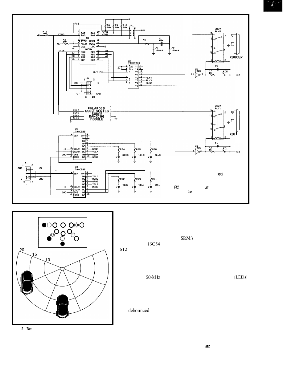
r
JCER
Figure l--The motorcycle blind
scanner
uses a single ultrasonic ranging module but
selects among five transducers using relays. A
processor handles the coordination and
generates display.
Figure
LED display and associated bird’s eye view offer five
zones and three distance ranges.
including a microproces-
sor, a decoder, a driver,
and two serial-to-parallel
shift registers. While any
small micro will do, I
chose the smallest PIC
available-the
words of code
space)-and still used
only half of the available
RAM and code space.
Mechanical relays
direct the HV
bursts from the single
ranging module to one of
the five transducers.
Each transducer covers a
45” zone. The relays are
fully
prior to
releasing the burst of
energy and remain
energized while the
ranger listens for an
echo. Since the relays are going to be
running continuously, mechanical life
becomes a factor. Mechanical life is
listed at about 10 million operations.
My maximum duty cycle (limited by
the
maximum listening time) is
2.5 cycles/second. That’s 9000 cycles/
hour or about 1111 hours. On the
motorbike, it would last over 60,000
miles at 60 mph.
While most of the electronics are
within the enclosure that mounts on
the rear of the bike, the display
needs to be in front of the driver. A
five-conductor shielded cable connects
the two pieces of circuitry. Power,
ground, and three shift register
signals-data, clock, and latch-are
used. Each shift register has eight
latched-output bit positions and a
serial output (used for chaining).
Fifteen outputs are needed-one for
each of the three distance zones within
The Computer Applications Journal
Issue
September 1994
63
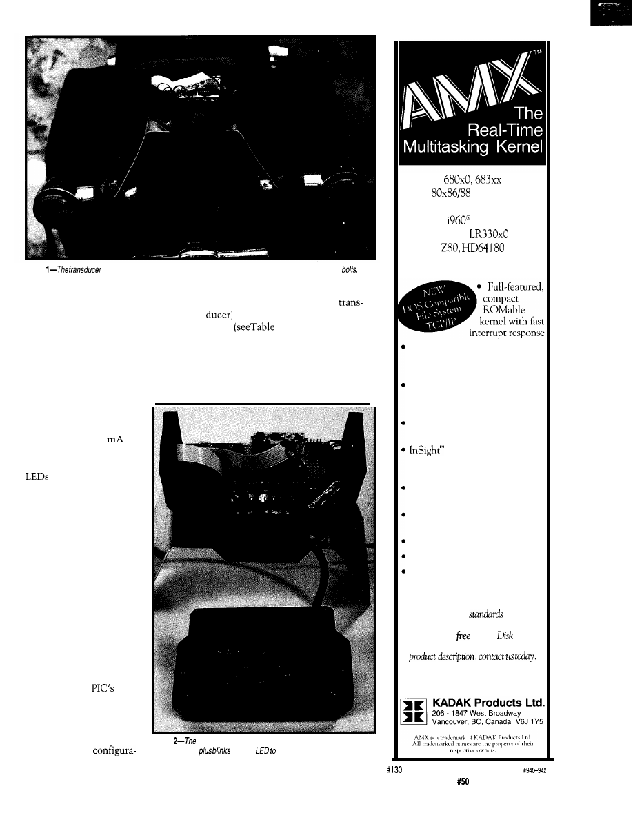
Photo
package mounts on the back of the motorcycle using some spare luggage rack
the
five regions.
At the
last minute,
I
tion jumpers are used to choose the
made use of a sixteenth bit to provide
alert points (distance from the
a heartbeat
LED just to verify that the
for each of the three colored
system is actually executing.
zones
1).
The electrical system of most
Configuration 0 is used for testing
vehicles is very noisy, so I used a hefty
purposes for those of you who don’t
hash choke and capacitor on the input
have 30’ rooms without obstacles. The
to cut the noise prior to the 5-V
maximum distance of the sonar
regulators.
I
used one regulator for the
ranging module is about 35’ and is
microprocessor (and
display circuitry) and one
for the SRM. The system
requires about 300
operating current (depend-
ing on the number of
on) plus about 2 A
during transducer bursts.
Using separate regulators
prevents current spikes
from affecting the micro.
A good-sized, heat-sinking
surface became available
when I constructed a
mounting bracket from
aluminum scraps I had
laying around the shop.
GO WITH THE FLOW
If you refer to the
flowchart in Figure 3, you
will see how simple this
control program is. After
initializing the
ports, the configuration
port is read. Eight possi-
bilities can be selected,
although at present I am
using four. The
Photo
handlebar display unit shows three distances in five
different zones
another
show it’s alive.
real mode
80386 protected mode
family
R3000,
Features
Preemptive, priority
based task
scheduler with optional time
slicing
Mailbox, semaphore, resource,
event, list, buffer and memory
managers
Configuration Builder utility
eases system construction
Debug Tool is available
to view system internals and
gather task execution statistics
Supports inexpensive PC-hosted
development tools
Comprehensive, crystal clear
documentation
No-hiclden-charges site license
Source code included
Reliability field-proven since 1980
Count on KADAK.
Setting real-time
since
1978.
For a
Demo
and your copy of our excellent AMX
Phone: (604) 734-2 796
Fax: (604) 734-8114
See us at Embedded Systems West booths
The Computer Applications Journal
Issue
September 1994
6 5
Data Genie offers a full line of test measure-
ment equipment that’s innovative, reliable and
very affordable. The “Express Series” of stand-
alone, non-PC based testers are the ultimate
in portability when running from either battery
or AC power.
Data Genie products will be
setting thestandards for quality on the bench
or in the field for years to come.
HT-2
The HT-28 is a very convenient way
of testing Logic
and
Tests
most
and DRAM’s
It can
also identify unknown numbers on
74 and CMOS
series with the
‘Auto-Search’ feature.
$189.95
14
The HT-14
EPROM writer
with
a
super fast programming speed
that supports devices from 27328 to
27080, with eight selectable pro-
gramming algorithms and six pro-
gramming power
selections.
$289.95
P-300
The Data Genie P-300 is a useful device that allows you to quickly install
on cards or to test prototype circuits for your PC externally. Without having to
turn off your computer to install an add-on cards, the P-300 maintains com-
plete protection for your motherboard via the built-in current limit fuses.
$349.95
M I N G
M i c r o s y s t e m s
Division of MING 6 P.
17921 Rowland Street
of Industry, CA 91748
TEL (818)
912-7756
FAX
912-9598
Data Genie products are backed by a full
limited factory warranty.
limited by maximum amplifier gain,
which is used to hear those distant
reflected echoes.
Next a channel (transducer) is
selected and a short,
loop
is entered which assures the relay’s
contacts are settled prior to enabling
the HV transmitting pulses. Raising
on the SRM begins the measure-
ment cycle. Every millisecond, the
ECHO line is polled for a logic high
which would indicate that a reflected
echo has been detected. The elapsed
time is saved, and the routine is ended.
Now the elapsed time register is
compared to each of the zone points
originally set by the configuration
jumpers. The first three bits of the
present channel’s status register are
updated with either or to indicate
whether there is a target in or out of
the three zones. These first three bits
of each of the channel’s status register
are shifted out to two external shift
registers located in the display. Green,
yellow, and red
are connected to
the shift register’s outputs. Each
channel’s status bits should end up
shifted out to the corresponding LED.
Finally, the channel is incremen-
ted (or cleared) and a jump made back
to the top of the loop. Loop timing is
dynamic and based on the time needed
to receive an echo (or timeout).
PROS AND CONS
There are some disadvantages to
using a single SRM and multiple
transducers. With five transducers,
each zone can be updated 2.5 times/
second. At 60 miles per hour, a target
travels 88 feet per second. Since 88
divided by 2.5 is 35 feet, a target can go
from out-of-range to crashing-into-you
in a single sample time. Fortunately,
we are concerned with relative speeds
(i.e., the difference between your speed
and the speed of the approaching
target). This is usually under
10
mph
which is about a car length per second.
Decreasing the number of trans-
ducers or increasing the number of
improves the update timing.
You must determine what rate is
necessary for your particular applica-
tion. In robotics, you might use eight
transducers in a 360” pattern and still
have better than I sample/second
issue
September 1994
The Computer Applications Journal
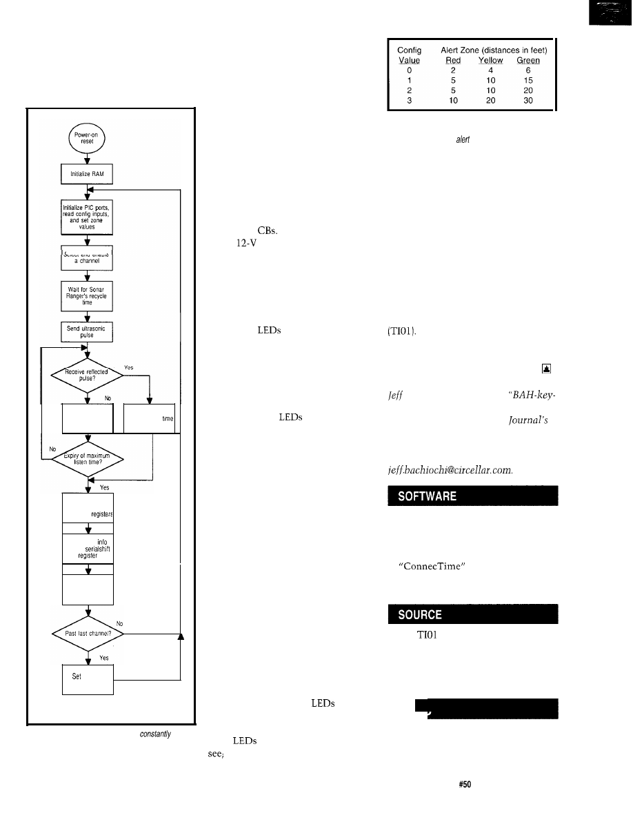
using only a single SRM. (If I were to
use eight transducers to get a full 360”
display of my driving arena, I would
add a second module and get better
than 3 samples/channel/second.)
Select and enable
1-ms delay loop
Save reflected
Compare channel
zones and update
LED status
Send status
through
Increment channel
channel
number to zero
Figure 3-The P/C’s control program
polls
each ultrasonic transducer and displays fhe results on
the operator console.
The display I am using reminds
me of fuzzy logic. It’s not so important
for me to know the exact distance;
however, I do want to know if an
object is far, near, or close and whether
it is approaching or falling back.
ROAD TEST
Securing the transducer assembly
to the rear of the motorcycle is easy
(see Photo 1). Bolts for mounting an
optional luggage rack are presently not
used. When a small group of “the
guys” go camping in the spring and
fall, we like to keep in touch with each
other using
So, I already had a
handy
connection available right
underneath the passenger seat. I fished
the display cable beneath the seat and
tank and mounted the display to the
handlebars. I donned my helmet and
was ready to cruise.
Leaving the parking lot, I quickly
noticed the
extinguishing. The
clutter of the lot was gone and all I
was registering was the guardrail along
my right side. As I made my way
through a small neighborhood, parked
cars blipped the display. While waiting
for “the green” at the expressway’s
entrance, all the
illuminated one
by one as vehicles pulled in around
me.
Now for the highway test. I
proceeded up the ramp accelerating to
meet a pack of roaring semis. I don’t
enjoy being boxed in between 18
wheelers so I pulled into the middle
lane and let traffic zoom around me on
both sides. The display activity
coincided with the traffic movement.
However, the activity in the two
corner zones could be improved a bit.
The next exit brought me back
into stop-and-go town traffic. The
vehicles were much closer now and
the display reflected this. I contem-
plated this while making my way to
the Circuit Cellar world headquarters.
EPILOGUE
This project won’t end here. There
are three improvements I want to
make. First, the colored
I used
are difficult to see in the daylight
because they are tinted with color.
Clear
would be much easier to
they actually change color.
Table l-The unit can be configured for one of four
operating modes, with each mode using a different set
of ranges for the three
zones.
Second, I would like to supply
each transducer with its own defined
zone definitions. This way the corners
can use larger zones than the sides or
the back.
Last, I’d like to mount a switch on
the display panel to control one of the
configuration switches. This would let
the driver change zone definitions
from a city setting to a highway
configuration on the fly.
This project uses Polaroid’s
standard transducer which comes with
the SRM offered by Circuit Cellar Kits
Have fun experimenting with this
project. I hope to meet you somewhere
out there on the road. Happy trails!
Bachiochi (pronounced
AH-key”) is an electrical engineer on
the Computer Applications
engineering
staff.
His background
includes product design and manufac-
turing. He may be reached at
Software for this article is avail-
able from the Circuit Cellar BBS
and on Software On Disk for this
issue. Please see the end of
in this issue for
downloading and ordering
information.
The
ultrasonic ranger is
available from Circuit Cellar Kits,
4 Park St., Vernon, CT 06066,
(203) 875-2751, fax: (203) 872-
2204. Price is $79.
419 Very Useful
420 Moderately Useful
421 Not Useful
The Computer Applications Journal
Issue
September 1994
6 7
Tom
PID-Pong: Point, Set,
Match: Using a Hitachi
H8 for Real-time Control
PID-Pong challenge
overcome. The victor’s name is
PIDDLE (PID Design, Learning, and
Experimentation), a combination of a
high-integration,
micro running
PID software and monitoring software
on a PC.
For those of you who missed last
January’s article
Chal-
lenge,”
the original goal was
to develop an interesting and educa-
tional platform to serve as a
control-demonstration vehicle. The
result was the PID-Pong machine, a
incorporating a ping-pong ball,
plastic tube, 12-V fan with PWM
(Pulse Width Modulator) motor
controller, and a Polaroid
Ultra-
sonic ranger (see Figure 1 and Photo
1).
PID-Pong is able to sense and
control the ball position, so the
challenge is to move the ball quickly
and accurately between setpoints. I
was delighted to discover that the
machine isn’t a pushover. Indeed, it’s
practically uncontrollable by mere
humans. Due mainly to severe (i.e., a
second or so) fan inertia [“lag” in
speak), the usual result is the
pong ball shoots out of the tube in a
mortar-like fashion.
You’d be amazed at the amount of
havoc a flying ping-pong ball can
wreak in a cluttered office. It calls to
mind the chaos theory parable of a
butterfly flapping its wings causing a
hurricane an ocean away. Well, the
ping-pong ball taps the messy pile of
magazines, that slides into the coffee
cup, which sloshes on the disk..
Having a machine but needing a
controller, I took Thomas Edison’s
words, “Genius is 1% inspiration and
99% perspiration,” to heart. Thus,
99% of the credit for PIDDLE goes to
Aleksander Hanslik, Andrzej Sitek,
and Mirek Chojnacki of Hanslik
Software Laboratory (Katowice,
Poland). They are to be congratulated
for writing a lot of great code while
tactfully disabusing me of my more
outlandish inspirations.
YAP, YAP, YAP
Before describing PIDDLE, I guess
now’s the time to launch into the
obligatory Yet-Another-PID discourse.
I can pursue one of two tacks.
First is the complex math treatise,
complete with lots of differential
equations, Z-transforms, Bode plots,
Routh’s Criterion, and so on. Fortu-
nately for me, those who are capable
and so-inclined can refer to any
number of well-written tomes. In
particular, I relied on the “Control
Theory” chapter of the Instrument
Engineer’s Handbook
and
Venczel, Chilton Book Company,
ISBN# o-8019-7290-6).
Another approach is to reference a
real-world situation such as braking a
car for a stoplight. I like this idea, but
this particular oversimplified analogy
fails because it underestimates the
skill (and foolishness) of all but
time drivers. In fact, seeing
making phone calls, drinking
coffee, fixing their hair-indeed, all at
once-indicates that driving is practi-
cally an open-loop process these days.
Back in the days when “muscle
car” meant more than a taxi full of
professional wrestlers, one popular
“benchmark” was the 0-100-O test in
which the goal was to go from a
standing start to 100 mph and back to
68
Issue
September 1994
The Computer Applications Journal
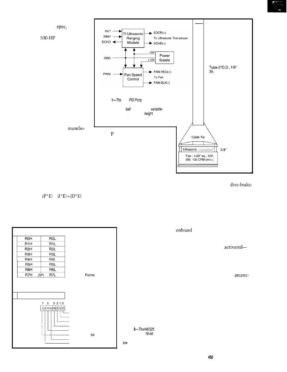
a stop in minimum time. Unlike the
typical O-60 or %-mile
this
reflected justifiable concern about the
mismatch of a
motor against
feeble drum brakes and iffy tires.
In these days of asthmatic
wimpmobiles, a more realistic driving
analogy is the Type-A executive
driving a rent-a-wreck. You’ve surely
seen such stoplight-to-stoplight Marios
and probably wondered how they made
it through childhood without reading
The Tortoise and the Hare. That’s
what makes driving (and process
control) interesting-real-world
“constraints” (“If I don’t get to that
meeting on time, I’m history”) and
“disturbances” (death-wish pedestri-
ans, flat tires, bad gas, etc.).
So, let me just leave the
jumbo behind and keep it as simple as
I can (which is real simple). PID refers
to the Proportional, Integral, and
Derivative control technique. The
control output is set depending on P, I,
and D functions of the “error” which
is simply the difference between the
current position-where you are-and
the desired-where you want to be
(i.e., the setpoint)-state. Thus,
O
U T P U T
=
+
Actually, various combinations of
the factors are possible. P-only, PD, PI,
and PID are most often used.
Figure
basic
machine uses
an
ultrasonic ranging
module to determine
the position of the
in the tube.
A
speed fan is used to control the
of the
ball.
7
0 7
0
D affects the output based on the
rate-of-change in the error. Consider
an unsuspecting RV backing into the
street 100 feet ahead. Without a D
factor, the P-only braking response
will be the same whether you’re going
10 or 100 mph, the latter case likely
leading to a particularly ugly case of
“terminal overshoot.”
I is a little more subtle and refers
to an accumulation of previous errors.
The best example is the
Joe or Jane Procrastina-
tor who insists on
driving with worn-out
brakes. Though they
drown the brakes’ dying
screams by turning up
the radio, eventually
they notice they’re
stopping halfway into
the intersection. The I
term belatedly kicks in
and they begin to adapt,
first by braking earlier
and when that gets old,
Register
perhaps resorting to
abusive downshifts,
S
P
:
S
t
a
c
k
7
0
PC
PC: Program Counter
CCR: Condition Code
Carry flag
Overflow flag
Zero flag
Negative flag
Half-carry flag
Interrupt mask
User bit
User bit
The term is the most obvious
and simply means the output varies
directly with the error (i.e., the
difference between a leisurely and a
panic stop).
Figure
register file
consists of eight
registers
that can be accessed in high or
B-bit chunks.
thick,
(min.) length
Manifold (ex: ice bag)
Transducer
Fan Guard
length spacer
Fan Guard
flinging the doors open in a
like manner, using their briefcase as an
anchor, and so on.
Other PID embellishments have
their corollary on the road. Output
limiting used to be a simple byproduct
of the fact that the pedal would go to
but not through the metal. Today,
micros actively limit output
with ABS (antilock braking system)
and TCS (traction control system). The
latter are usually switch
after all, you can’t blame someone
who spends enough to buy a heap that
can get out of its own way for wanting
to “light ‘em up” once in a while.
“Antireset windup” is an
sounding term describing exceptional
start-up situations in which the state
initially (i.e., at reset) resists change. In
this situation, an integral term can
accumulate outrageously (i.e., “wind
up” resulting in overshoot while it
“unwinds”). Consider the poor fool
who stalls his car when the lights turn
green. Invariably, even an otherwise
smooth driver will launch frantically
when they finally get it started. You
see, they’re simply trying to “unwind”
The Computer Applications Journal
Issue
September 1994
69
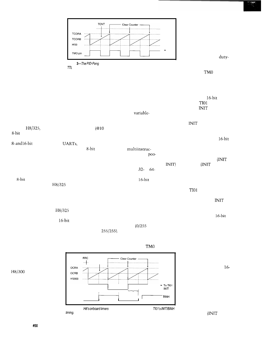
H’FF
TO
Fan
PWM
timer-output pin is auto-
matically inverted on each
match with the FRC (Free
Running Counter). Thus,
having loaded TCORA with
255 and started the timer,
setting the fan power is as
simple as poking the
Figure
machine’s fan is controlled by a single pulse-widfh-modulated
cycle
factor into TCORB.
bit.
The PWM output dutifully
Finally, PID calcula-
tions can be tweaked to
deal with a degree of the
nonlinearity that character-
izes many real-world
control problems. A car
analogy is the way throttle linkage (or
software in emerging “fly-by-wire”
systems) damps initial throttle
response in the interest of smooth
starts, lest parking lot maneuvers turn
into destruction derbies.
this, the RISC concepts are tempered
with various doses of reality.
proceeds via
with
absolutely no further software inter-
vention required. Nice!
For instance, instructions occupy
either two or four bytes, which
represents a tradeoff between code
density and circuit size or speed,
factors which are, respectively,
enhanced and degraded by
length instructions.
Talking to the PID-Pong
machine’s ultrasonic sensor is also
easy, thanks to the smart
timer/
counter. Driving the
calls for two
outputs to toggle the
and BINH
(Blank Inhibit] lines with a phase delay
representing the “blanking time” (i.e.,
the delay from
to BINH in which
the ECHO input should be ignored to
avoid false detection). Well, check out
Figure 4, and you’ll see that the
units, two output-compare registers
(OCRA, OCRB), and output pins
(FTOA, FTOB) handily fill the bill,
establishing both the sampling
to
and blanking
to BINH)
time.
the integral error of their
ways, no doubt encouraged
by the honking and hand
gestures of the myfarcating
Type As behind them.
SMALL BLOCK H8
Casting about for a suitable
PIDDLE engine, we settled on the
Hitachi
a relatively low-cost,
single chipper featuring a healthy
complement of on-chip I/O, including
timer/counters,
parallel I/O, and so on.
Deciding up front to use C, the
ugly specter of bloated code raises its
head. Any of you who have actually
tried to cram a C program (especially
with floating-point calculations] onto
an
single-chip CPU know what
I’m talking about. The
packs a
relatively whopping 32 KB of ROM/
EPROM and 1 KB of RAM on chip,
hopefully keeping “OUT OF
MEMORY” messages at bay.
Similarly, instruction execution
time
MHz) varies from 200 ns to
1.4 us (MLT/DIV) with a likely average
of 300-400 ns or so for a typical mix,
which is quite competitive with other
micros. Sure, the
tion-per-clock RISC zealots would
poo such numbers, but they should
keep in mind the H8 probably costs
less than the socket for their
or
bit Superdupers.
The timer/counters (one
and two S-bit) deserve special exami-
nation since it turns out that they
mate very well with the PID-Pong
machine.
Architecturally, the
is
blessedly simple. The register file
(Figure 2) consists of eight
registers which can be accessed in high
or low S-bit chunks as well. Thus,
most of the 57 basic instructions are
offered in byte and word versions.
But, it gets even better. The
feedback from the PID-Pong machine
(i.e., ball position) is determined by
monitoring the
ECHO output.
The idea is to measure the elapsed
time between the assertion of
and the receipt of ECHO, with posi-
tion determined by the speed of sound.
Well, what do you know-the
timer/counter also includes an input
capture pin (FTI) that, when asserted,
latches the value of the FRC into an
input capture register (ICR).
The somewhat minimalist
instruction set reflects the
migration of RISC concepts
off the desktop and into
controllers. Notably; the
is a “LOAD/
STORE” machine in which
all instructions reference
only registers with the sole
exception of loads and
stores (MOV on the H8)
that shuffle operands and
You’ll remember that the output
from the PID controller to the ma-
chine (i.e., the fan speed setting) is a
single pulse-width-modulated TTL bit
that sets the fan duty cycle
through
As shown in Figure
3, the S-bit timer easily handles the
task-thanks to two timer-compare
registers (TCORA, TCORB). The
Thus, once everything is rolling,
determining the ball position is as
H’FFFF
FTOA
FTOB
Blanking
I n t e r v a l
results to and from
Figure 4-Jha
can a/so automatically hand/e the
memory. However, beyond
7 0
Issue
September 1994
The Computer Applications Journal
simple as reading the ICR
whenever you want-it will
always contain the most
recent ECHO time. The
bit unit doesn’t have the
feature to automatically
toggle the output pins so
OCRA and OCRB interrupt
handlers are required.
However, they are short (3
instructions) and sweet
since they only need to
toggle the pins
and
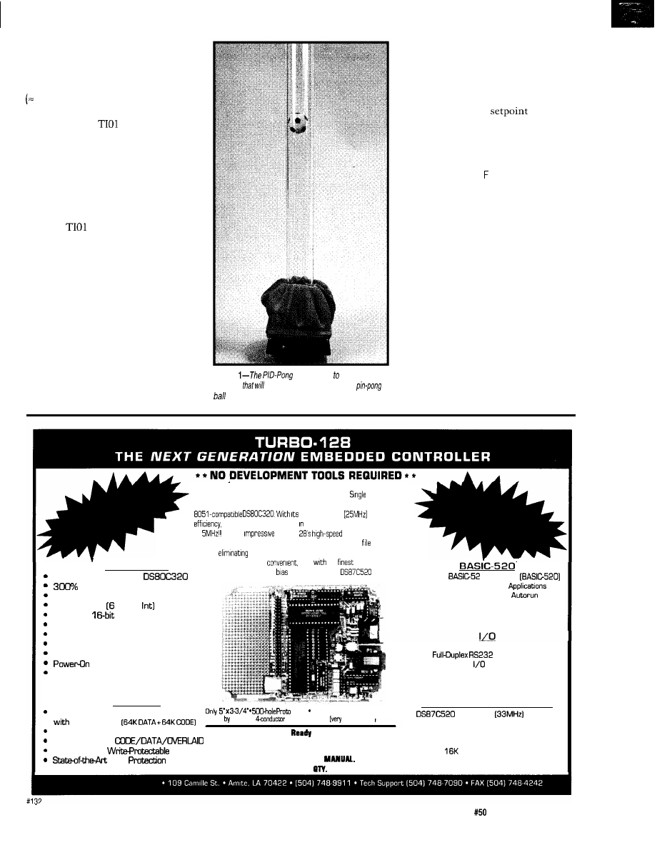
BINH pins, respectively), clear the
interrupt, and return. Noting the
sampling rate is a leisurely 20 Hz or
so, a little calculation shows “trivial”
0.01%) is the right word to describe
interrupt overhead.
Getting the
working is one of
those things that’s easy-after you’ve
done it. Ironically, the major stum-
bling block isn’t the I/O timing, but
the fact the darn ECHO pin is “al-
most” TTL compatible. I myself have
spent more time than I care to admit
head scratching over an “almost”
working
before I remembered to
put a stupid pull-up on ECHO.
Fortunately, all H8 inputs (including
FTI) offer internal pull-ups-just
remember to enable them in software.
I “C” A SOLUTION
Besides a little ASM to set up the
timers, return the ball position, adjust
the PWM, and so on, the rest of
PIDDLE is written in C. It was a
pleasant surprise to find the entire
routine was only a couple of hundred
lines, the guts of which (P I D LOO P) are
Photo
Challenge is come up with
a scheme
automatically
maintain the
in one position in a tube on a cushion of air.
shown in Listing 1. Let’s step through
it, and you’ll see that it’s actually
quite straightforward.
As expected, the PID loop starts
by calculating the current error (e)
which is simply the
(x) minus
the current ball position (y).
The next few statements are by far
the trickiest and require a little more
explanation. The goal is to derive a
nonlinearity factor
( N
L) that is
applied to change the gain depending
on the magnitude of the error. When
the ball starts to move to a new
setpoint, the error is large and high
gain is called for. However, as the ball
approaches the new setpoint, gain
should be reduced for finer control.
The nonlinear version eases what’s
otherwise a “choose your poison”
juggling act between high (may
overshoot or oscillate) and low (slow
response] gain.
This adaptation relies on RFACT,
a
tuning factor which controls the gain
multiplication. Roughly speaking, the
gain is doubled for every RFACT
percent increase in error. Thus, if
R
EADY TO
P
ROGRAM IN
BASIC
OR
A
SSEMBLY
Photronics Research
Introduces the T-128 A True
Board BASIC
Development System The T-128
IS
based on Dallas Semiconductor’s new
2X clock speed
and 3X cycle
an Instruction can execute 160ns an 8051 equivalent speed of
62
Equally
IS
the T-l
NVRAM Interface Any
of the 128K RAM may be programmed directly from a PC
through the
console,
EPROMs and associated tools Program Development has
P R O C E S S O R
never been faster or more
even
the
EPROM emulator
,
.
Dallas Semiconductor’s
The T-128 features PORT 0
and EA-select for
upgrade
l
Modified
interpreter
more efficient than the 8051
Three 1 B-bit Timer/Counters
13 Interrupts Ext, 7
A second
Data Pointer
384 Bytes of Internal RAM
Programmable Watchdog
Brownout Protection
Power-Fail Reset/Interrupt
Reset
Fully supported by Frank/in C
M E M O R Y
Entire 128K Memory Map populated
fast NVRAM
All memory programmed on-board
Partitionable as
Code Space is
Data
Area Console/Power connected
a single
telephone wire
convenient]
Comes
to
Run
with power adapter/cable assembly.
Includes utility diskette with
DETAILED TECHNICAL
$199
in
Now
Fast
Enough
for New
l
Stack BASIC Pmgrams and
l
CALL ASM Routines for Maximum Speed
l
Three S-bit Parallel Ports
l
Two
Serial Ports
l
Decoded Device
Strobes
l
SO-Pin Bus Connector
UPGRADE [available soon]
l
processor
l
Instruction cycle: 121 ns
l
8.25 MIPS
l
8051 equivalent: 82.5 MHz
l
Internal
ROM/l K SRAM
l
Runs BASIC 800%
faster!
The Computer Applications Journal
Issue
September 1994
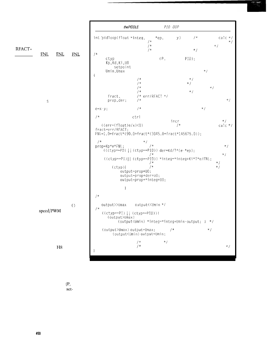
RFACT is small, the nonlinearity is
high and vice versa as shown by
cranking some sample numbers
through the following calculation:
10
30
100
ERROR%
10
2.35
1.34
1.09
20
5.18
1.78
1.19
30
10.37
2.35
1.30
Next the proportional, derivative,
and integral gains are calculated [note
F N L's role) as necessary, depending on
the controller type in effect (P, PI, PD,
or PID). Similarly, a
w
i t c
h statement
builds the final output for a particular
controller type from the component
terms.
Some embellishments follow the
raw calculation. The next few state-
ments show integral “windup” (here
called “saturation”) prevention, but
note that they have been commented
out since antiwindup conflicts with
the nonlinearity algorithm. The next
two statements simply limit the
output [fan speed) to empirically
defined minimum and maximum
values.
Finishing up, the current error
(e)
is made the previous error
(e p)
which
will be used to calculate the derivative
[change in error) on the next pass
through the loop. Finally, the calcu-
lated output is returned to ma i n
where the fan
is set
using the S-bit timer as previously
described.
TIME FOR A TUNE-UP
The “Dashboard,” which runs on
the PC (it’s written in Turbo C) and
communicates with the
via serial
port, is the final piece of the PIDDLE
puzzle and performs two key func-
tions.
Via menu selection, the Dash-
board allows all key parameters to be
defined and downloaded to the H8
including the controller type PD,
PI, PID) and associated gains,
points, the previously described
RFACT nonlinearity factor, maximum
and minimum fan output, and stability
criteria.
Once everything is set up, the
game begins. Under control of the
Listing l--The core of
control code is the
L
routine.
int
word
PID-loop
integ integral part of controller
ep preceding control error
y process output
this function uses global variables such as:
type of controller
PI, PD,
constants of controller;
x
range of the output control signal
float output:
output control signal
int e:
actual control error
float err,
normalized 0 to 1 control error
FNL,
nonlinear gain factor
prop and deriviative parts of regulator
calculation of actual error
RFACT sets the
action nonlinearity by causing the factor
FNL to double for every RFACT %
in controller error
if
err=-err;
normalized error
output calculation
calculation of proportional part
if
calculation of deriviative part
if
calculation of integral part
switch
calculation of output signal
case
P:
break;
case PD:
break:
case PI:
break:
case PID: output=prop+der+*integ+UO;
when using nonlinear algorithm antiintegral saturation
correction may cause improper action of controller when
or
if
antiintegral part sat correction
if
*integ=*integ+Umax-output:
else if
if
output limiter
else if
*ep=e;
new error
return output:
return the object controlling magnitude
Dashboard, the H8, and PIDDLE
software try to swing the ball back and
forth between setpoints. On each pass
through the PID loop, the H8 reports
the state (i.e., ball position and fan
speed) to the PC where it is displayed
strip-chart style (Figure 5).
As you can see from the figure,
PIDDLE does a great job. Notice how,
underneath the smooth response of the
ball, the fan is going through hoops.
This highlights the PID-Pong chal-
lenge-imagine trying to achieve the
same results twisting a knob.
Tuning the PID equations (i.e.,
choosing the controller type, gains,
and RFACT) is a fairly ad hoc process
of experimentation. A common
strategy (the “Ultimate Method”
described in Liptak and Venczel) is to
choose a P-only control setup and
increase the gain until the system
72
Issue
September 1994
The Computer Applications Journal
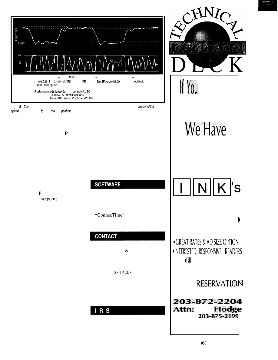
Results: #Steps=25 Time 0 0100
Max. overshoot unknown Max. undershoot unknown
Equation
F
+
+ 0.005
+ 140.0
Filename:
Description:
Comments Initial comment
Options
Fan
Stability criteria:
00%
Error criteria
Figure
Dashboard screen
printout
illustrates just how impossible if is for a mere human
fan
quickly enough keep ball
stable.
oscillates (i.e., the ball bounces
around, but never stabilizes on the
setpoint). Then, back off the gain
and start fiddling with the other stuff.
Derivative action and/or RFACT can
be tweaked to reduce the step response
over/undershoot at the expense of
rise/fall time. Integral action deals
with intrinsic variabilities such as the
fact that the fan output is higher when
it warms up, atmospheric conditions,
or airflow restrictions (try placing
your‘finger over the top of the tube).
In a sense, the and D terms get the
ball close to the
quickly and
the I term helps “nudge” it into
place.
An intriguing possibility given the
computing power at hand would be to
make the system auto-tune itself. The
PC could try various equations and
measure the results. Tweaking could
proceed algorithmically along the lines
described in the previous paragraph or,
if you’re in no hurry, more or less
randomly. Just let the thing crank for a
few hours (days, weeks?) while you
head for the beach and come home to a
finely tuned setup.
Another idea would be to check
out the fuzzy approach in which the
PID calculations would be replaced
with a series of “rules” along the lines
of IF ERROR IS X AND BALL SPEED
IS Y THEN SET FAN TO Z.
The good news is I’ll put all this
stuff on my list of things to do. The
bad news-that list is real long and
never seems to get any shorter so don’t
hold your breath. In the meantime,
feel free to challenge the PID-Pong
machine to a match of wits.
q
Tom Cantrell has been an engineer in
Silicon Valley for more than ten years
working on chip, board, and systems
design and marketing. He may be
reached at (510) 657-0264 or by fax at
(510) 657-5441.
Software for this article is avail-
able from the Circuit Cellar BBS
and on Software On Disk for this
issue. Please see the end of
in this issue for
downloading and ordering
information.
Hitachi America, Ltd.
Semiconductor IC Division
2000 Sierra Point Pkwy.
Brisbane, CA 94005 18 19
( 4 1 5 ) 5 8 9 - 8 3 0 0
Fax: (415)
Hanslik Software Laboratory
ul. Huculska 18
40-736 Katowice, Poland
011-48-21-524-261
422
Very Useful
423 Moderately Useful
424 Not Useful
Have
The Product,
The Market
Circuit Cellar
T E C H N I C A L
P O S T C A R D
D E C K
READERSERVICE
FAX YOUR
SPACE
TODAY!
Sue
Or
call
Deadfines:
Space 9-20-94
Materials 1 O-l -94
The Computer Applications Journal
Issue
September 1994
73
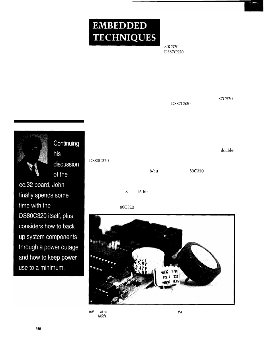
John Dybowski
Fast Processors, Big Caps,
and Ring Oscillators
0
ast month, I
described some of
the more conspicu-
ous features of the
microcontroller. This new
offering from Dallas Semiconductor
not only reaffirms the viability of
processors for new and demanding
applications, but, by virtue of its sheer
processing power, bridges the perfor-
mance gap between and
devices. In light of Dallas’s past
achievements, it should come as no
surprise that the
is just the
first of a new series of processors
destined to give some of the bigger
chips a run for their money.
Already, Dallas has announced its
next generation silicon based on the
processing core. The
contains 16 KB of EPROM,
1 KB of RAM, and operates all the way
from DC to 33 MHz. Since high-speed
operation implies a higher level of
power consumption, this new and
improved architecture provides some
very interesting features designed
specifically to reduce the electric bill.
There’s even a version that adds a
built-in real-time clock to the
the
Naturally, the inclu-
sion of a built-in timepiece necessi-
tates an external backup power source
that is also used to back up the
1
KB of
on-chip RAM.
Interestingly, the recommended
backup power source is not the usual
lithium cell that Dallas has become
famous for. Instead, the preferred
backup source is a battery-like,
layer capacitor, known as a
supercap.
But, I’m getting ahead of myself
here. Having barely scratched the
surface of the
I’m telling you
about silicon that’s just now becoming
available. This can be dangerous stuff.
You’ve got to be careful since working
with even the second or third cut at a
new processor can prove to be more
than enough to satisfy your need for
adventure. Being the first one in line
Photo 1-Supercaps are starting to appear in different shapes and sizes. While their appearance might be confused
that
ordinary battery, they are rechargeable and don’t exhibit
same memory effects as shown by
typical
7 4
Issue
September 1994
The Computer Applications Journal
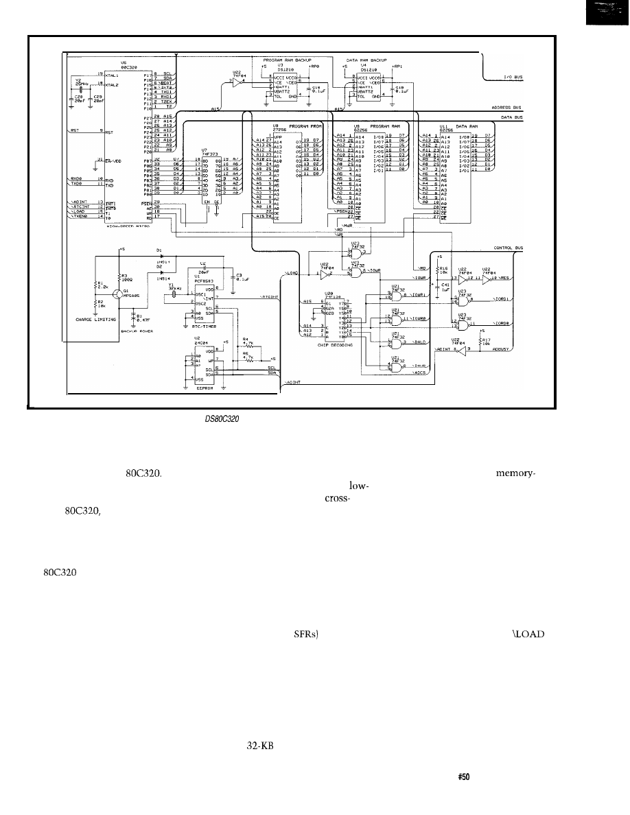
Figure l--The ec.32 is based on the Dallas Semiconductor
processor and includes everything needed to set up an embedded data collection system.
minimal. Coupling such hardware
PROM and data RAM begin at 0 and
can be downright reckless. Let me get
back to the ec.32 embedded computer.
Then, I’ll tell you about supercaps and
a little more about the
with a resident kernel and a PC-hosted
debugger results in a potent, integrated
development vehicle. The addition of a
PC-based simulator along with a
cost cross-assembler and C
compiler rounds out the system. This
is the ec.32 embedded computer.
program RAM is located at 8000h. The
upper half of the data area at 8000h is
allocated to the system’s
mapped peripherals. This sparsely
populated peripheral I/O area is,
obviously, loosely decoded.
THE ec.32
The
unlike the newer
Dallas family members (with on-chip
EPROM), requires external program
memory to operate. Most applications
also need external data memory since
the
comes with only the usual
256 bytes of internal data RAM. I
personally like an embedded computer
that supports downloading executable
programs directly into the target.
EPROM emulators work okay, but
having this capability built into the
computer allows you to use this
feature beyond the design phase and
extend it into your end system.
Providing a built-in download
capability does imply that special
hardware considerations be addressed
early in the design phase, but the
overall system impact can be kept
All things considered, the basic
803
1
architecture offers a fairly
expansive addressing map for an 8-bit
processor. This address map is also
what tends to drive compiler develop-
ers nuts. With the program memory,
internal data memory, external data
memory, and bit addressable memory
(not to mention the
that all
overlap, it’s a wonder these code
generators don’t choke.
The areas internal to the chip are,
naturally, fixed. The memory regions
that we can exercise control over are
the external data and program areas. In
an effort to keep things simple, the
ec.32 partitions this program/data area
into four
blocks, where program
Although the program and data
segments physically overlap, they are
kept separate by independent read
strobes: \PSEN for program memory
and \RD for data memory. Through
special gating of the \WR strobe,
program RAM can be written to.
During normal operation, program
RAM is not writable, but this capabil-
ity can be enabled by pulling
(P3.5) low via firmware. Asserting this
pin has the effect of degating the \WR
strobe to the peripheral section and
instead routes it to the program RAM.
This enables useful functions such as
loading of executable programs and
setting breakpoints.
Since the hardware, resident
kernel, and PC debugger are closely
The Computer Applications Journal
Issue
September 1994
7 5
coupled, I could have saved the
port pin and instead controlled this
write-enable gating directly from the
PC using a modem control line. I
elected not to do so since I wanted to
retain this powerful capability for
application programs that didn’t make
use of the system’s built-in debugging
capabilities. Realize, however, that the
resident kernel is designed for effi-
ciency since it uses no RAM and
consumes less than 2 KB of code
space-it could ride along with just
about any application program.
With 32 KB of program PROM you
can burn a lot of functionality into the
PROM and still be able to download
sizable programs and functions into
the
program RAM area. This
downloadable program RAM can hold
transient programs for performing
diagnostic or analyses functions,
replacements for major application
routines, complete application pro-
grams, or big lookup tables.
The basic bus arrangement of the
ec.32 is shown in Figure 1. The
connects, in the usual manner,
via a transparent address latch to the
and peripheral bus
members. Chip-select and
support gating are implemented
conventionally. The only unusual
thing here is that FAST logic is used
exclusively for the discrete logic.
Picking up speed in the glue logic, as I
explained last month, results in the
ability to run with slower PROM,
RAM, and peripheral chips.
The configuration shown requires
a
program PROM and a
program RAM. The data RAM must be
a
part if full-speed operation is
required. With one stretch cycle, a
common
part is adequate.
Unless you really need the extra
performance, it might make sense to
leave the data access rate set to the
default one stretch cycle. As I’ll
demonstrate next month, some of the
system peripherals need that stretch
cycle to remain within specifications.
Also shown in Figure is the
throughput-serial peripheral bus. This
supports a number of periph-
eral functions that don’t need to
operate at the full bus bandwidth. For
this serial bus, the familiar two-wire
is used. Local
support is
provided for 5 12 bytes of
using a
The PCF8583
timer handles a number of time-
keeping tasks for the system and,
additionally, provides 256 bytes of
nonvolatile RAM. Contained within
the PCF8583 is a real-time clock/
calendar and a fully programmable
interval timer that is wired as an
interrupt source. The
is carried
through to a four-pin modular RJ- 11
connector and can be used to attach a
companion LCD/keypad module or
additional digital or analog peripherals.
THE TROUBLE WITH BATTERIES
With program and data RAM and
an RTC, it’s obvious that some form of
backup power must be provided to
make these functions nonvolatile.
Often a lithium cell is selected since
many of the more popular nonvolatile
controllers are specifically designed to
work with lithium characteristics.
However, a nonrechargeable cell will
Integrated
software development environment including an
editor with interactive error detection/correction.
Access to all hardware features from
Includes libraries for RS232 serial
and precision delays.
Efficient function invocation mechanism allowing call trees
deeper than the hardware stack.
Special built-in features such as bit variables optimized to
take advantage of unique hardware capabilities.
Interrupt and A/D built-in functions for the
Easy to use high level constructs:
#include
any key to
khz
w h i l e
1
PCB compiler
$99 (all 5x chips)
PCM compiler
$99 (‘84, ‘71, ‘84 chips)
Pre-paid shipping $5
COD shipping
$10
CCS, PO Box
Milwaukee WI 53211
414-78 l-2794 x30
LCD PANEL METER
-Available now at an unheard of
price of
$15
plus h
N e w ! N o t s u r p l u s !
Specifications:
Maximum input:
additional ranges provided through
external resistor dividers
Display:
LCD, 0.5 in. figure height,
jumper-selectable decimal point
Conversion: Dual slope conversion, 2-3
readings per sec.
Input Impedance:
ohm
Power: 9-12 VDC 1
DC
Circuit Cellar, Inc.
4 Park Street, Suite 12,
Vernon, CT
0 6 0 6 6
Tel: (203) 875-2751
Fax: (203) 872-2204
76
Issue
September 1994
The Computer Applications Journal
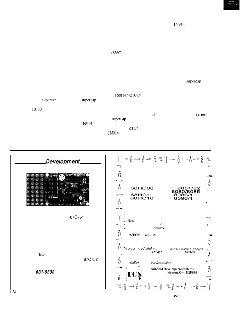
eventually have to be replaced. Even
with rechargeable types, there is a
limited service life. This is a shame
since you can bet your controller will
end up in some totally inaccessible
area and you’ve undoubtedly designed
it to otherwise last forever. Given the
available choices, maybe you’ll find it
surprising that I suggest not using a
battery at all.
When supporting low-drain CMOS
loads, good results can be achieved
using a capacitor as a backup power
source. However, not just any capaci-
tor can be used for this purpose.
Electric double-layer capacitors, more
popularly known as supercapacitors,
are specifically designed as a backup
power source. This
technol-
ogy offers low leakage and a volumet-
ric efficiency
times that of the
most compact, aluminum-electrolytic
capacitor. This means you can squeeze
1 F of capacitance into less than a
cubic inch.
Supercaps offer several advantages
over conventional batteries. They
don’t need periodic replacement. The
charge rate is not at all critical and can
range from microamps to amps. They
have no polarity and can’t be damaged
by reverse connection. They are
inherently safe and will not leak or
explode under temperature extremes
since they contain very low electrolyte
levels. Typically, they are rated to
operate from -40 to
Charging
and discharging a rechargeable battery
causes a chemical reaction that
typically cannot be repeated more than
several hundred times. In contrast,
charging or discharging supercaps is a
physical, not chemical, phenomenon
that does not cause damage.
The backup circuit shown in
Figure 1 uses an NEC
F
that feeds two DS1210
nonvolatile controllers that, in turn,
supply power (and provide protection)
to the program and data RAM. A tap is
also taken off of the
through
a
diode that is used to deliver
backup power to the PCF8583
timer. A separate
isolates the
main 5 V and feeds the RTC when the
system is active.
Normally, in such a backup
scheme, you’d want to use better
diodes than the
that I selected.
In this case, however, little advantage
would be gained since the PCF8583
can operate all the way down to 1 V
and the signal pins can exceed VDD by
1 V. Having made the rather cavalier
statement that there’s nothing to
charging a supercap, you may well
wonder why I’ve placed a handful of
parts in my charging path. Let me
explain.
In principle, there’s no reason why
you couldn’t hook your
directly to the system’s 5-V rail.
However, in such an arrangement, the
inrush current would be limited
primarily by the supercap’s ESR. The
specification for the 0.47-F part I am
using shows this parameter to be about
13 This justifies the 100-R
limiting resistor (R3) that limits the
power supply burden during the initial
current inrush.
This explanation still leaves
several other components in the
charging circuit unaccounted for. The
Speed Your
Process
By Using Our Controllers!
We offer an array of controller boards and
software tools for the 8051 and
families of
m i c r o c o n t r o l l e r s . C o m p l e t e p a c k a g e s a r e
available to help you develop your projects. We
also have a selection of add-on peripherals such as
LCD and keypad interfaces.
Features:
l
Breadboard area
l
Flexible
arrangement
l
Powerful controller BASIC for the
l
Simulators
P h : ( 7 0 2 )
l
F a x : ( 7 0 2 ) 8 3 1 - 4 6 2 9
Iota Systems, Inc.
POB 8987
l
Incline Village, NV 89452-8987
C C O M P I L E R S
CROSS ASSEMBLERS
D E B U G G E R S
6 8 0 9
8 6
9 6
A
Low Cost!! PC based cross development packages which
include EVERYTHING you need to develop C and assembly
language software for your choice of CPU.
MICRO-C compiler, optimizer, and related utilities.
A
Crow Assembler and related utilities.
l
coded (efficient ASM) standard library (source included).
Resident monitor/debugger source included)*
Includes text editor,
software and many other
utilities.
a
and
kits do not include monitor/debugger.
Each Kit: $99.95 + s&h (please specify CPU)
Reg. $49.95, only
with purchase of
Developers Kit (above). Offer valid until October 31, 1994
write for
of development tools.
P.O. Box 31044
C A N A D A
Tel/BBS: 613-256-5820 Fax: 613-256-5821
The Computer Applications Journal
Issue
September 1994
7 7
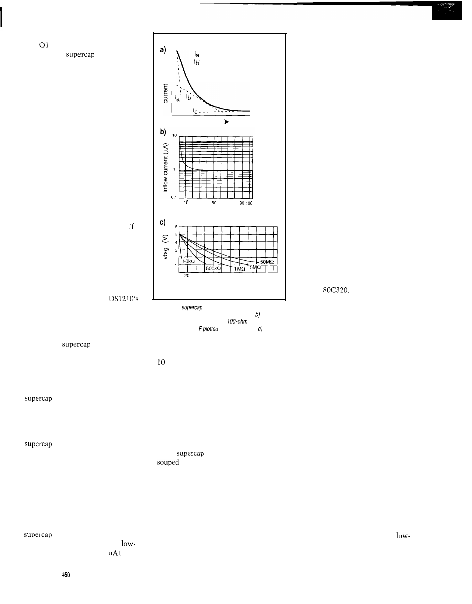
emitter-follower composed of RI, R2,
and
limits the maximum voltage
to which the
can charge.
Although limiting the charging
voltage diminishes the ultimate
backup time somewhat, it’s neces-
sary to ensure proper operation of the
DS1210 nonvolatizers.
Briefly, the DS1210 protects its
associated RAM by providing power
from either the system 5 V or from
the backup power source. Addition-
ally, chip select is routed through the
DS1210 and is held inactive when
operating in backup mode, thereby
protecting the RAM.
It seems the DS1210 doesn’t
actually monitor the VCC pin for the
presence of 5 V but, instead, looks at
the internal voltage that results from
mixing the VCC voltage with the
voltage from the backup battery.
this internal voltage is above the
selected threshold level, the part
won’t go into backup mode when
VCC goes away. Obviously, this
renders the part useless and has dire
consequences for the associated
RAM. This threshold level is depen-
dent on how you strap the
TOL pin. But, regardless of the
setting, you won’t have any problems
if the backup power is kept some-
where under 4 V.
Since a
is, after all, still
a capacitor, you might conclude that
given enough charging current, a full
charge could be attained in a matter of
seconds or minutes. Although this
may be true in a sense, when a
is charged, it actually goes
through several distinct phases.
A closer examination reveals that
there are actually several aspects to
the charging current that flows into a
through these various phases:
*recoverable charging current that can
be reclaimed when the capacitor
delivers backup power
*absorption current that cannot be
recovered on discharge
*leakage current
It is only during the last stage that the
exhibits minimum leakage
current and therefore attains a
level of self-discharge (l-2
A
Charging current (CC.)
Absorption current (A.C.)
ic: Leakage current (L.C.)
time
0
20 30 40
60 70 80
time (h)
al
2
0
40 60
80 100 120 140 160 180 200220
time (h)
Figure 2-A
can be characterized by a) various
current components flowing info the supercap, the
expected inflow current through a
source
impedance into 0.47
against time, and several
representative discharge curves.
Unfortunately, this only occurs after
or more hours of charging.
So you shouldn’t knock yourself
out trying to reduce your circuit’s
current consumption to inordinate
levels since, after a point, the
capacitor’s own leakage current will
predominate and may ultimately
swamp any imagined power savings
you can attain.
By now, I’m sure there’s no doubt
that a
is more than just a
up capacitor. It should be
evident it has electrical properties
different from other capacitors.
Because of these differences, projec-
tions of backup time based on familiar
calculations may be misleading. First
of all, the capacity or the amount of
energy available will be less at high
than at low discharge rates. And, for
extremely light loads, the supercap’s
internal leakage current will dominate
and be a greater loss than the circuit
being backed up.
To further complicate matters,
the capacitor’s leakage current
decreases drastically as the voltage
decreases. Additionally, a typical
CMOS load cannot be characterized
as a constant current or a constant
impedance and, as a result, also
changes as the backup voltage
decays. These factors complicate an
accurate prediction of backup time
for a given set of parameters. Best
results can be attained by studying
the manufacturer’s specifications
and discharge curves along with
some breadboarding and empirical
observations.
Figure 2 illustrates the various
current components flowing into a
supercap, the expected inflow
current through a 100-n source
impedance into 0.47 F plotted
against time, and several representa-
tive discharge curves.
RINGS OSCILLATORS AND
CRYSTALS
The
like all CMOS
circuits, consumes more power at
higher operating frequencies than
when running slowly. In many
system configurations, maximum
performance is the overriding
concern and power consumption
may not even be an issue. However,
there are circumstances under which
we must stipulate both a high level of
performance and low power consump-
tion. These conflicting criteria repre-
sent a certain class of portable and
battery-operated instrumentation.
The saving grace to this seeming
paradox is that, although low power
and high performance are mutually
exclusive, you needn’t deliver both
simultaneously. A popular hack is to
organize the system to remain idle for
extended periods and to operate in
high-speed bursts only in response to
external events. This tactic drives the
average power consumption way down
yet leaves the door open to full-speed
processing when necessary. Under
such circumstances, it’s beneficial to
use one of the processor’s built-in
power operating modes while waiting
for something significant to happen.
78
Issue
September 1994
The Computer Applications Journal
Like the
1, the
supports two power-saving modes of
operation. IDLE mode suspends all
processing operations by holding the
program counter in a static state. This
saves a considerable amount of power
particularly when operating with
external memory since the bus is kept
inactive. While using about half the
power of a fully operational system,
IDLE mode keeps all clocks active.
The serial port, timers, watchdog, and
power monitor are all kept functional;
the processor can instantaneously
respond to any interrupt condition.
STOP mode provides the lowest
power consumption by stopping all
chip clocks. No processing is possible,
and all timers and serial communica-
tions are shut down. This state results
in current consumption of
l-2
STOP mode can, of course, be
exited via a reset. This reset can be
externally generated or be the conse-
quence of a power fail reset. Note that
the power fail reset and power fail
interrupt require the use of the
internal band gap used to
monitor VCC. To conserve power, the
band gap is turned off by
default when STOP mode is entered.
Although turning off the band gap
results in significant power savings,
the processor could potentially be
thrown out of control should a power
dip or brownout occur since a clean
reset would not be generated. This is
not the case with a full power failure
since normal band-gap operation is
restored on a power-on reset. In any
case, should a brownout be a possibil-
ity, the band gap should be turned on
via firmware prior to entering STOP
mode. In some cases, this may be
undesirable since it increases the
current consumption to about 100
A second, more useful means of
exiting STOP mode exists which
involves the use of an interrupt. One
restriction is that an internally
generated interrupt can’t be used since
there is nothing going on inside the
processor when it is
An
external interrupt can be used without
restriction, or a power fail interrupt
can be used provided the band gap is
enabled. Although keeping the
processor in the STOP mode most of
the time realizes maximum power
savings, it’s important to restrict
speed operation to the absolute
minimum amount of time.
In a traditional implementation, a
significant amount of power can be
wasted waiting for the oscillator to
come up to speed and stabilize before
meaningful operations can be per-
formed. The crystal startup time could
exceed the actual processing time if
only a short operation need be per-
formed. This scenario portrays the
default condition for the
since
the crystal oscillator must delay
65,536 clocks before full-speed
execution can begin. Needless to say,
this can really put a drag on perfor-
mance. The
addresses this
problem with an internal ring oscilla-
tor that can start instantaneously.
The extended interrupt SFR EXIF
contains the bit EXIF. 1 that,
when set by firmware, enables the
to use its ring oscillator to
come out of STOP mode without
waiting for the crystal oscillator to
start. The ring oscillator provides an
instantaneous start up, but is not
accurate. Generally, this isn’t a
problem since the firmware usually
performs a short task and returns to
STOP mode. The crystal oscillator is
started up when STOP mode is exited,
but is not available until 65,536 clocks
are counted. If an accurate
is
required, the code has no choice but to
wait for this startup delay to expire
before beginning its time-critical
operations.
EXIF.2 can be interrogated to
determine from which clock source
the processor is operating. This bit is
set when the ring oscillator is used and
is cleared by hardware when the
crystal oscillator kicks in. If it turns
out that you do need the accuracy of a
crystal timebase, at least you can get
your preliminary setup out of the way
and be ready to roll by the time the
crystal comes on-line.
Although the
takes
fundamental
power-saving
capabilities to new extremes, you can
expect further refinement in upcoming
processors in this family. Already, the
and
have defined new
power-management modes:
and
PMM2. Normally, the CPU performs
an instruction cycle every 4 oscillator
clocks. In
this time is ex-
tended to 64 clocks. With PMM2, this
goes out to 1024 clocks. You can
operate in
keeping the proces-
sor alive, and still consume less power
than in IDLE mode. And, these newer
processors let you totally shut down
the crystal amplifier and operate
exclusively from the internal ring
oscillator. Even when running off the
ring oscillator, you can realize the
benefits of
and
prescalers.
AND THE WINNER IS...
Next month I’ll conclude my
description of the ec.32 with a discus-
sion of the analog and digital I/O,
power supply, and other miscellaneous
system elements. I’ve spent consider-
able time working with the ec.32, yet I
still find myself at times surprised at
just how quickly it runs. Still expect-
ing the status quo, I guess.
q
Dybowski is an engineer in-
volved in the design and manufacture
of embedded controllers and commu-
nications equipment with a special
focus on portable and battery-oper-
ated instruments. He is also owner of
Mid-Tech Computing Devices.
may be reached at (203) 684-2442 or
at
For elements of this project,
contact:
Mid-Tech Computing Devices
P.O. Box 218
Stafford Springs, CT 06075-0218
684-2442
Individual chips are available from
Pure Unobtainium
13 109 Old Creedmoor Rd.
Raleigh, NC 27613
Phone/fax: (9 19) 676-4525
425 Very Useful
426 Moderately Useful
427 Not Useful
The Computer Applications Journal
Issue
September 1994
7 9
The Circuit Cellar BBS
200/2400/9600/l
bps
24 hours/7 days a week
(203)
incoming lines
Internet E-mail:
We have quite the gamut of topics this month. First, we consider
what’s necessary for doing a closed-loop control scheme and how to
trade off digital and analog sections. Next, we talk about whether it’s
best to condition low-level analog signals right on a plug-in board or
outside the main computer.
Use an existing
or come up with something tailored to the
application? That’s the question we debate in the next thread.
Finally, back to
issues and a quest for reference books that
spell out in terms mere mortals can understand.
Control loop feedback
8154
From: JOHN DAVID COOK To: ALL USERS
Can anyone recommend a good simple book to explain
control loops? Basically I’m looking for “Feedback Loops for
Dummies” or something that will explain the dynamics of
the darn things intuitively so I can read it.
I ask for my robot which uses two independently driven
wheels tied together in a software control loop so that it
goes straight when told to. The problem is that the error
between the two wheels tends to “run away” and send the
robot spinning, literally as the loop overcorrects and both
wheels spin full in opposite directions.
Msg#: 8168
From: BEN MEHLMAN To: JOHN DAVID COOK
can’t recommend a book but I have two suggestions.
First, vary the amount of correction in proportion to
the error; that is, if the robot is only slightly off course,
speed up the slow wheel SLIGHTLY and give it time to
catch up. What is happening is you haven’t taken the
inertia of the robot into account. You need to give the robot
time to change course.
Second, limit
much correction you apply. Since
you probably have a good idea how much slippage there’s
going to be, set realistic limits on the maximum correction
and the maximum time it can be applied. This will prevent
it from losing control.
Msg#: 8419
From: PAUL SHUBEL To: JOHN DAVID COOK
“Simple” control algorithms are not easy to
by.
Most of the articles I see are only one notch below
82
Issue
September 1994
The Computer Applications Journal
tions of the IEEE. Their use by anything but “control
engineers” is doubtful. I always hark back to the early years
of microprocessors (sigh] when magazines were filled with
article after article on “basic” techniques with micros.
8603
Is this a sure sign of positive feedback?
From: JOHN DAVID COOK To: BEN MEHLMAN
There are a couple things I didn’t mention before: when
velocity is set to zero, the ‘bot is very unstable; a slight
bump can cause it to spin. Also, if the velocity of one wheel
drops to zero while turning, it will spin. I theorize that the
ratio of error over velocity is going to infinity as velocity
drops to zero.
Msg#: 8673
From: JAMES MEYER To: JOHN DAVID COOK
Not necessarily. (How’s that for an answer?)
If
I
were writing the code, I’d start with some simple,
testable, routines that could be combined later into a more
complete program.
Some fundamental routines to start with include:
l
Measuring the distance that each wheel turns.
Revolutions * Circumference of wheel.
*Speed of each wheel. Distance time unit.
Then use the speed as feedback in a loop so that you
can command a particular speed and have the software
maintain that speed in the face of variations in load on the
motor.
Note that you can do this early in development
without a complete ‘bot-just a motor, tachometer, com-
puter-controlled current source, and a method of inputting
the speed command. Note carefully the term “current
source.” Motor speed control is *much* easier if you
control the applied current rather than the voltage.
Until you can do something like this, trying to debug a
more complicated system will probably be impossible. The
idea is to “divide and conquer.” Take a complex task and
split it up into smaller tasks. Each so simple that they
*have* to work. Then build on success. You’ll always know
at what point something new goes wrong, so fixing it
should be easier.
Msg#: 8677
From: GEORGE NOVACEK To: JOHN DAVID COOK
There are numerous good books on the market (the
classic here is “Automatic Control Systems” by Benjamin
Kuo) dealing with closed-loop systems. Some books do not
go beyond the PID controller, others go further into Kalman
filters, predictive control and fuzzy controllers. The bad
news is that unless you enjoy calculus, transforms, and
similar advanced math disciplines, you will not enjoy these
books. Still, they will explain to you the theory behind it,
but will not tell you how to design it.
Math is no longer such a problem thanks to the PC, as
there are numerous programs out there which will let you
calculate as well as simulate closed control loops. They
range from freeware through a-couple-thousand-dollar
packages such as
to $20,000 wonders such as Easy
5. The problem is it is not the controller but the actuators
and the mechanical parts which will eventually defeat you.
Unless you can get a reasonably accurate transfer function
of these mechanical parts (in my years in design of embed-
ded controllers
I
rarely saw them), your simulations will
only confirm the old computer adage “garbage in, garbage
out.” Therefore, it is more than likely you will end up
tweaking. I hasten to defend analytical methods: High
performance in closed-loop controllers (such as head
positioning in hard drives] would never be achievable by
tweaking. But keep in mind these people manufacture
millions of those at close tolerances and, therefore, can
develop proper data. You can’t.
Speaking out of experience: if there is no special reason
to close the loop digitally, don’t! It is hard to beat a $1
amp where no special adjustments calling for digital control
are needed. As a rule, I use a micro to generate the position
command to the loop, then in many cases go to a DAC and
close the loop in analog. Even many dynamic adjustments
of the loop function can be done in the analog loop by using
digital gain control, multiplying
and so forth. If you
need a PID and don’t want to play with different RC values,
you can be inventive and do the proportional term with an
op-amp while generating the integrating and derivative
terms in software. There are many ways to skin a cat.
The main problem you are going to run into with a
real-time controller is the lack of time. You suggested that
you are controlling a robot. I venture to guess that, if it is a
motion of the robot you are controlling, the critical fre-
quency of your system will be in the
area. Unless you
can acquire all the data within no more than a IO-ms period
sampling rate), you are asking for aliasing prob-
lems. But things get even worse. You cannot just use each
and every sample you acquire for control. Digitization noise
will kill you. You have to filter the signal: averaging is most
common, convolution can give you almost an order of
magnitude better S/N ratio. Depending on the system, you
will need probably 5 to 9 samples. This takes not only
processing time, but inherently introduces lag into the
system, which will not be very beneficial to its stability.
The lag that the frequency limiting of the feedback is
introducing at this rate can also cause deterioration of your
phase margin and lead to oscillations. Furthermore, you
must update your loop calculation at the same rate (every
10 ms), or you will have a *very* hard time keeping the
loop stable due to the processing lag. If not accurately
controlled, you can actually go into positive feedback. The
integrating term will need some limiting (it can saturate the
controller; many systems enable the I term only within a
small position error range). You must also make sure there
is no roll-over of the integration. A
will be hard
pressed to keep up at this rate, even if there is nothing else
for it to do, especially if you code in C. So, if you do not
have to use Kalman filters and have a DSP on board, don’t
mess around with digital.
Because you probably will not have transfer functions
to do any meaningful calculations, you will end up having
to tweak the system, analog or digital. Disable both I and D
terms and get the proportional term working correctly.
Then add I and tweak it. Last, add the derivative term. The
Circuit Cellar INK
had a good article several years ago with
a very detailed procedure how to do it.
Analog signal conditioning
Msg#: 8540
From:
WEST To: ALL USERS
Is
it good design practice to do analog signal condition-
ing inside the PC? As an example, let’s just say I would like
to boost the gain of an incoming signal by 100 or 1000.
Would it be better to condition the signal outside the PC’s
environment at that level of gain? And are the
power supply lines on the bus clean enough to use, or is it
better to regulate and filter this it down to a lower voltage.
Msg#: 8674
From: GEORGE NOVACEK To:
WEST
It depends. From the packaging, construction, and
convenience standpoint, it is much easier to design a
in card, stick it into an expansion slot inside the PC, and
forget about it. But there are caveats!
One, the power inside the PC is limited and is not very
clean. There are methods to get around in my view the
best bet is in putting an independent regulator on board.
Getting clean, 12-V signal from the digital 5-V supply is no
longer a big deal.
The Computer Applications Journal
Issue
September 1994
8 3
Two, the EM1 environment is not exactly very clean
either, be it through conducted (mainly ground bounce) as
well as radiated emissions.
So it mainly depends on the impedance of the circuits
you are going to design, especially at the low signal level
and the bandwidth you will be working with. You will have
to keep the PCB traces as short as possible; use SMT
components if you can and in the end you may have to put
a metal can around the analog front end. If you have never
used I2 or more bit digitizers, be prepared for a little blood
bath. PCB layout and proper grounding is something you
will have to learn by experimenting. I would strongly
recommend that you use a four-layer board with proper
ground and power planes. Keep in mind basic rules such as
the 5-V digital power traces must not run on top of the
analog ground. You are dealing with fast-rise-time pulses,
which generate very high frequency spectrum and even
minute capacitances between PCB layers can cause un-
wanted coupling.
It all depends on your requirements. Eight-bit resolu-
tion is easy. Ten bits will get slightly demanding. Anything
over ten is unforgiving. I am talking about digitization, but
it applies equally to just pure amplification. If you have a
signal which you are jacking up to 5-V range and then
digitizing to eight bits, you still have to look at the
significant bit level divided by the gain to establish the
noise level your system will accept. If you do not have
experience with low-level circuits, it might be easier for
you to put the module outside the PC, with its very own
power supply. Then, at least, you will know that the
problem is within your module, not some radiated coupling
through the air from God knows where.
8801
From: PETER HAND To:
WEST
It’s
pretty noisy in there, but you can do it if you’re
careful about shielding and grounding. A lot depends on
what’s in the next slot, too. You may have problems if it’s a
video adapter.
The
power supply lines on the bus are usually
horrible, and it’s easier to start with a reasonably clean
supply than try to filter a dirty one. Consider using a DC/
DC converter to generate
V from the 5-V supply; so
much the better if the output ground is isolated. Working at
V gives you a bit more headroom to work at higher
voltages.
I presume you’re about to tackle a 12-bit ADC project.
Be warned-it will take your knowledge and patience to the
limits and beyond. I’d use a multilayer PCB with a continu-
ous ground plane, and not allow any digital
including the 5-V supply-anywhere near the front end.
84
Issue
September 1994
The Computer Applications Journal
DMX-512 or something else?
Msg#: 6230
From: VIC MANZO To: ALL USERS
I’m Looking for a microprocessor-controlled UART that
does serial transmitting and receiving in xl6 mode at 250
kbps. If possible, a dual version. I’ve tried all the Philips and
National Semiconductor products but have not come up
with acceptable availability times on then. If anyone has
used or knows of one, please let me know.
Msg#: 6280
From: BEN MEHLMAN To: VIC MANZO
The National PC16550 can do 250 kbps. This chip
might be in short supply now due to strong demand in the
PC market, but at least you know it will be in production
for a while! It uses
a xl6
clock, so a or
clock will
get you 250 kbps with a divisor of 2 or 4.
I assume you are generating DMX-5 12 for lighting
control? I am specifically interested in lighting control
projects of this nature. I have constructed a prototype
circuit using the 16550 to generate Colortran protocol
(DMX at a lower speed). Unfortunately, I am having a
channel jitter problem with it which I originally thought
was due to an unstable mark-after-break period. After a
little troubleshooting, I believe the trouble is in my
to-computer (PC parallel port] interface timing, so the chip
itself has not been ruled out as suitable for the task.
I’m also trying to get info on the Siemens
166
microcontroller and ilk. This microcontroller has two
internal
capable of greater than 250 kbps, and
sufficient processing speed and internal RAM to offload the
entire communications task to the one chip. Unfortunately,
I can’t find Siemens to get the info on it! Does anyone have
their USA phone number? I know they have an evaluation
kit which they give away, lend, or sell real cheap..
8598
From: VIC MANZO To: BEN MEHLMAN
As a matter of fact, I am going to use it for DMX-512 as
well as other lighting protocols including Colortran. How
did you become interested in lighting control? I work for a
company called BASH lighting in New Jersey. Maybe you
have heard of us! I also own my own company called
Logical Lighting Interface Inc. I don’t think you’ve heard of
that one. Our company designs and manufactures interfaces
for lighting. We are starting to get into designing specialty
items such as radio-controlled dimmers. If you need any
help with you project, let me know.
I think I’m going to have to design my circuitry for the
National
or the
Because it is used in PCs, I
think I would have a good chance of it being more available
than others. I am also looking into the Philips version of the
same UART. They apparently just redesigned their part and
it has become available.
Thanks for your suggestion.
If you are considering using a micro for you project, try
the Dallas
out. It has two
and a bunch of
other neat little toys.
8761
From: BEN MEHLMAN To:
What you’re doing is interesting to me. I am mostly
into software now, and I’ve been working on lighting
console software for an embedded PC-type board. It’s
coming along well although the concepts have shifted
rather dramatically since I started! I’m using a test system
now which consists of a DMX/Colortran protocol adapter
and a small manual console with just the grand master, one
split crossfader, and a few of the more important buttons on
it. Both of these plug into my PC or laptop. I have been
recently working to license this software to a board manu-
facturer. Of course, as usual, finishing it would be a good
idea, too.
8681
From: PETE CHOMAK To:
I just happened to read this message, and it looked like
you might have some info I need. I built a large camera
crane/boom with a remote control pan-tilt head a while
back
24 hour-per-day rush project), and now I am
working on a proper servo system for the head (I used a
variable-voltage drive and center-off momentary toggles
initially). I plan on using a PIC for the control, with the
position commands received from a PC-based controller via
a serial link (preferably on XLR audio cable). It occurred to
me that I should give the controller an address so I can
build other similar controllers and use them on the same
bus. Then it occurred to me that that is what DMX-512
does. I don’t want to reinvent the wheel, so do you have, or
know where I can get the full DMX-5 12 specs?
8760
From: BEN MEHLMAN To: PETE CHOMAK
The DMX
can be purchased from the USITT (U.S.
Institute for Theatrical Technology) for less than $20. The
is simple, so I’ll explain it.
The physical interface is a standard RS-422 line. The
connector type is specified as a
XLR-type connector,
with an optional second pair of wires for two-way commu-
nications (few DMX devices use this, and no software
is written for reverse communications).
The serial format is standard
asynchronous, with
1 start and 2 stop bits running at 250 kbps. The entire set of
levels for up to 5 12 dimmers are sent in a packet, and
packets are sent repeatedly, generally no less than 10x per
second, usually 20x or more. The
allows a much lower
repeat rate but, no one uses it.
Now for the packet itself: Send a “break” for three byte
times, followed by a I-bit “mark after break” followed by a
1 -byte DMX start code which is always zero. DMX receiv-
ers are supposed to ignore any packet with a
start
code. The start code is immediately followed by from 1 to
5 12 bytes of data, with one byte per channel to be con-
trolled.
Note that there is no error correction. Dimmers don’t
respond fast enough to need it (much). Your application is
different. You might want to defer responding to any value
that deviates from the last value received by more than
some amount.
Even though it’s kind of a
you should
seriously consider using it since it means that hundreds of
computerized lighting consoles will be able to control your
unit. Some of them could have it doing some really wild
stuff.
8822
From: PETE CHOMAK To: BEN MEHLMAN
Thanks, it sounds fairly simple, the only difference is
that I was planning on 16-bit position values, but 8 bits may
do, or I could use two addresses per axis. I would like to get
the “official
if you happen to find the address, but
this should get me going.
8829
From: BEN MEHLMAN To: PETE CHOMAK
Well, I can’t find the address. But here’s the phone
number for the USITT: (212) 924-9088. They are very nice
and you can order the document over the phone with a
credit card. They have other documents which are interest-
ing, too.
Regarding 16-bit values, this has become a problem in
lighting as well. Eight bits are enough to control the
brightness of a lamp, but not enough to control the position
of moving lights as smoothly or accurately as needed. But
there are a lot of manufacturers doing it anyway, either
using “smoothing” algorithms to generate intermediate
data points for less jumpy motion, or using two channels for
16 bits of resolution.
The two-channel method has been gaining some
popularity, and there are some consoles, built with features
to support moving-light programming, that give the user 16
bits of control range on one control, sending the output on
two DMX channels. There has also been some activity
lately of trying to nail down a formal
for
control.
I am not up on the latest status of this.
The Computer Applications Journal
Issue
September 1994
8 5
Anyway, depending on how your camera is used, I have
a suggestion for you. Allow one DMX channel to control
the upper 8 bits of your motor position, giving that control
a “coarse” control of the entire pan range. Then, allow a
second channel to control an
range of values which
may or may not overlap the range of the first channel. In
other words, allow the second channel to modulate the first
channel, and allow the full-scale value of that modulation
to be
by the user.
if I need to do that. Bidirectional data is an interesting idea,
but I can’t think of any uses for it yet. Thanks.
ESD design references
Msg#: 7611
From: ROBERT MCILVAINE To: ALL USERS
So if the user, for example, is going to have all their
detail work being done in a 45” window, they set the coarse
channel to one edge of the range of interest, and use the fine
channel to move within the range. You may find that you
don’t need a true 16 bits of resolution after all. Use
16
bits
of control to generate perhaps only or 12 bits of motor
position information.
Can anybody recommend a source for info on ESD
protection design that might be obtained on the Internet or
a BBS? Something with tips and protection techniques or
design examples?
7635
From: ED NISLEY To: ROBERT MCILVAINE
8955
From: PETE CHOMAK To: BEN MEHLMAN
Interesting. I figured on 16 bits just because it is a neat
number, but 10 bits is probably enough, with better than
0.5” resolution for a 360” range. The smoothness and update
rate are particularly critical for camera positioning to allow
for acceleration and deceleration of a pan or tilt and for fine
framing, especially with a tight zoom. Thanks!
How about on a bookshelf? The book you want is
“Electrostatic Discharge and Electronic Equipment: A
practical guide for designing to prevent ESD problems,” by
Warren Boxleitner. It’s published by IEEE Press, ISBN
87942-244-O, IEEE order number PC02352, and will set you
back the usual 50 bucks or so that technical books seem to
cost nowadays.
You get lots of drawings that just don’t come through
very well in Internet-standard flat ASCII, too!
Msg#: 7642
From: VIC
To: PETE CHOMAK
From: ROBERT MCILVAINE To: ED NISLEY
DMX-512 runs at 250 kbps. As you probably know,
emulating asynchronous communications at this rate with
software using a super fast micro is hard. Using a PIC would
probably be impossible.
Thanks for the recommendation; I’ll pick it up. Basi-
cally, I have general knowledge of the topic. What I need in
the short run is to brush up so I can answer some questions
on Monday in a knowledgeable fashion.
I would suggest using an RS-485 data link but using a
synchronous style link. You shouldn’t think of creating a
protocol as “reinventing the wheel.” Protocols should be
created for a particular application. Creating your own
protocol also allows YOU to set the standard for your
controlling equipment. You don’t really need Joe Electronic
making controllers for your equipment.
If you have any overview type words of wisdom it word
be greatly appreciated. I will definitely check out the local
Barnes Noble for the book.
8065
From: GEORGE NOVACEK To: ROBERT MCILVAINE
Getting back to the point, I would also suggest you use
16-bit pan and tilt values if the system is to be digital. I
have found that using 8 bits doesn’t give the resolution or
the repeatability that is required, especially for camera
applications, Bidirectional links also have great advantages;
you should look into at least providing the hardware for
later software revisions.
Beside Ed’s suggested book, there is also “EM1 Control
Methodology and Procedures,” by Donald R. J. White
(Interface Control Technologies) and “Lightning Protection
of Aircraft,” by J.A. Plumer (Lightning Technologies). The
books are great references with lots of theory. I have not
seen any “cookbook” type publication. I am going to check
the one Ed suggested.
8652
10777
From: ED NISLEY To: GEORGE NOVACEK
From: PETE CHOMAK To: VIC
You
are probably right. I was thinking that by using
DMX-5 12, my controller would be able to also control
DMX-5 12 lighting gear. But I can probably build a translator
Do tell me (and everyone else!) what you think of
Boxleitner’s book in comparison to the others; I haven’t
done a review of the field and ought to know how it stacks
up. Thanks!
86
Issue
September 1994
The Computer Applications Journal
Msg#: 8675
From: GEORGE NOVACEK To: ED NISLEY
I have not read the book yet. I was going to order it,
wrote the particulars on a piece of a paper, and lost it. If you
would not mind giving it to me again, *promise’ not to
lose it this time.
I have read a few books on the subject, but have never
seen one which could be called a cookbook. All the works I
have seen (including a couple of magazines catering to the
ESD aficionados) are hardly understandable to people
without formal education in electrical engineering or
physics (and still remember their math). By the same token,
if you can understand those books, you really don’t have to
read them. They are forever rehashing what the
is and how it manifests itself. Not one tells you how
to get rid of it.
I have my personal suspicion (also due to knowing
several authors) that these guys are consultants. They want
to overwhelm the reader, show him how clever they are,
and convince him they are the only ones who can harness
the monster (for a price). They just stop short of calling it
“black magic.” I have not seen one work which would, in
specific terms, give the reader instructions how to proceed
in designing his equipment such that the ESD
EMP,
LSS) requirements are satisfied. And yet, the guidelines are
very specific and could be almost concentrated into a list of
dos and don’ts.
8718
From: ED NISLEY To:
GEORGE NOVACEK
One of those days, eh?
I think you’ll like Boxleitner’s book. For example, from
the summary in the “Enclosure Design Guidelines”
chapter:
1. The enclosure design must ensure that uninsulated
electronic components and lines have at least 2 cm arcing
distance from ungrounded metal objects that may be
touched by the operator.
6. All shield material must have an EMF within 0.75 V
(in the electrochemical series) of the metal they connect to.
If not, an intermediate metal connection device must be
used.
Can’t get much more specific than that, although, as he
points out, some of the guidelines are diametrically opposed
to each other and to guidelines required by, say, RF design.
That’s what engineering is all about..
We invite you call the Circuit Cellar BBS and exchange
messages and files with other Circuit Cellar readers. It is
available 24 hours a day and may be reached at (203)
1988. Set your modem for 8 data bits, 1 stop bit, no parity,
and 300, 1200, 2400, 9600, or
bps. For information on
obtaining article software through the Internet, send
mail to
Software for the articles in this and past issues of The
Computer Applications
may be downloaded from
the Circuit Cellar BBS free of charge. For those unable to
download
the software is also available on one 360K
IBM PC-format disk for only
$12.
To
on Disk, send check or money order
to: The Computer Applications Journal, Software On Disk,
P.O. Box 772, Vernon, CT 06066, or use your VISA or
Mastercard and call (203)
Be sure to specify the
issue number of
disk you order. Please add $3 for
shipping
U.S.
428
Very Useful
429 Moderately Useful
430 Not Useful
The Computer Applications Journal
issue
September 1994
87
Put My Money Where My Mouth Is
you probably already know, am an avid proponent of home control systems
When installed my
first system in ‘85, I justified its expense on the energy savings alone. Today it does so many more things that I
think of it as an electronic servant.
Besides turning inside and outside lights on and off, the HCS provides environmental control, security, and entertainment system
coordination, In fact, the environs which can be enhanced with a little electronic interfacing are almost limitless.
Of course, a quick reality check reveals that home control isn’t a quick drop-in installation like a toaster or TV. Lights and
appliances have to be wired to the HCS (or have wireless interfaces added). All this takes resources, persistence, and a compelling
purpose.
The thousand or so current Circuit Cellar HCS owners are a breed apart. So compelling was their goal that if we hadn’t presented
a packaged solution, they would have engineered their own. It was hardly a tough selling job.
Once you have satisfied the radical fringe, however, can you market an HCS like any other consumer product? In my opinion, at
present, no. Until
becomes a universally understood term like “VCR,” only the technically astute will appreciate its value enough
to make a purchasing decision. That “next” group is still the same CAJ readership.
Rather than a compelling goal, new users will base their decision on the three elements of any good investment: confidence that
they aren’t alone, justification that it makes sense, and instinct that the purchase is cost effective.
Well, have confidence that home control is not a flash in the pan. Meeting future national environmental targets dictates more
intelligent coordination among heating, air conditioning, and lighting. The Computer Applications Journal plans extensive coverage of
home control and building automation starting next year, complete with bonus editorial sections and supplemental offerings. We plan to
offer an extensive collection of construction projects including a
interface and broad coverage of the industry in general.
Second, with energy management and security as its primary use, a home control system hardly needs justification. The
hundreds of dollars saved yearly from extinguishing unneeded lights and intelligently controlling air conditioning and heating will help
pad the wallet. But it’s watching an unwanted visitor, at the
prompting, carefully retracing steps off your property as if negotiat-
ing a mine field that brings a smile to your face and a feeling of security to your mind.
And yes, finally there is the element of cost. Only you know what you will spend on a new idea. That’s something can’t predict.
What I can do, however, is make your decision easier by putting my money where my mouth is. I truly believe that you are
missing a great experience if cost is the inhibiting factor. To minimize your cost of entry into home control, I’ll give any
an
printed circuit board and the software to build a Circuit Cellar Home Control System free. The only cost to you is shipping
and perhaps a BBS call. See page 32 for details.
No, haven’t lost my senses, nor have I hit the lottery. What I do have is a dedicated interest in advancing technology for a
common goal. Nothing would make me happier than giving away thousands of DX boards. With that many users communicating and
contributing, the day that home control becomes as easy to understand as a VCR becomes that much closer.
Issue September
1994
The Computer Applications Journal
Wyszukiwarka
Podobne podstrony:
circuit cellar1996 09
circuit cellar2004 09
circuit cellar1995 09
circuit cellar1997 09
circuit cellar2000 09
circuit cellar1993 09
circuit cellar2001 09
circuit cellar2002 09
circuit cellar2003 09
circuit cellar1994 09
circuit cellar1996 09
circuit cellar2003 09
circuit cellar1997 09
circuit cellar1993 09
circuit cellar2004 09
circuit cellar1995 09
circuit cellar1996 09
więcej podobnych podstron