INK
The size is right. The power’s right.
The architecture’s right.
But, occasionally, there’s an exception. Take the
As a desktop
processor, it gained its popularity. Its processing power, low cost, and
familiar instruction set made it a prime candidate for embedded systems.
Although supplanted by the more powerful 2180, the
remains an active
participant in the embedded world, its popularity pushing it into many
embedded applications still active today.
Knowing the monetary power of the embedded market, newer
“desktop” processors anticipate the needs of an embedded system as well.
ARM processors quite capably drive the Acorn Archimedes computer as well
as the
Newton and
3D0. Here too, the embedded prowess of the processor
exceeds that of its desktop counterpart.
With the launch of Embedded PC, Circuit Cellar is placing its bet on the
embedded PC. Sure the size, bus, and power consumption of the desktop
PC has had to be rearranged for the embedded world, but it’s out of the
gate.
has exponentially accelerated it through the first stretch. How
long will it be until embedded PC revenue exceeds that of the desktop PC?
Embedded PC is a
quarterly insert devoted to bringing you the
latest on the embedded PC race. Feature articles will cover topics such as
off-the-shelf ISA-bus motherboards, expansion boards, networking, PCI,
other buses, and embedded PC software. With our columnists Rick
Lehrbaum and Russ Reiss, we gain a front-row seat on the PC/l 04 standard
and how to implement the embedded PC in real-life applications.
This month, David Prutchi shows us how to hot swap with an active
extender card for the ISA bus while Stefano
develops an ISA
bus simulator. Rick starts off with how PCMCIA makes a complementary
match with
while Russ overviews the embedded PC.
September theme of embedded applications overlaps with
Embedded PC.
Ed Lansinger gives us an engine control system based on
Motorola’s
Stuart Ball shows us how to debug when we’re short
of
and Gordon Dick covers both mechanical and electrical aspects of
building an XYZ router table.
And, of course, there are our
While Ed answers the
time question: Why emulate a 8086 at all?, Jeff begins a two-part series on
DC motor control using
Tom introduces us to the TSL230 intelligent
optosensor, and John finishes his series on Dallas Semiconductor’s newest
processor with power-management capabilities.
Notably, with this issue, John crosses the finish line and takes his
entrepreneurial enterprises on home. We salute John as he moves on to
other endeavors.
Janice Marinelli
Managing Editor of
Embedded PC
CIRCUIT
T H E C O M P U T E R A P P L I C A T I O N S J O U R N A L
FOUNDER/EDITORIAL DIRECTOR
PUBLISHER
Steve Ciarcia
Daniel Rodrigues
EDITOR-IN-CHIEF
PUBLISHER’S ASSISTANT
Ken Davidson
Sue Hodge
TECHNICAL EDITOR
CIRCULATION MANAGER
Janice Marinelli
Rose
EDITORIAL ASSISTANT
CIRCULATION ASSISTANT
Beth Andrix
Barbara
ENGINEERING STAFF
CIRCULATION CONSULTANT
Jeff Bachiochi Ed Nisley
Gregory
WEST COAST EDITOR
BUSINESS MANAGER
Tom Cantrell
Jeannette Walters
CONTRIBUTING EDITORS
ADVERTISING COORDINATOR
John Dybowski
Dan Gorsky
Rick Lehrbaum
Russ Reiss
CIRCUIT CELLAR INK, THE COMPUTER APPLICA-
TIONS JOURNAL
is published
NEW PRODUCTS EDITOR
monthly by Circuit Cellar Incorporated, 4 Park Street,
Harv Weiner
Suite 20, Vernon, CT
(203) 675-2751. Second
class postage
at Vernon, CT and additional offices.
ART DIRECTOR
One-year (12 issues)
rate U.S.A. and
Lisa Ferry
$49.95. All subscription orders payable in U.S.
PRODUCTION STAFF
funds only,
postal money order or
John Gorsky
check drawn on U.S. bank. Direct
orders
James Soussounis
and
related
Circuit Cellar INK
Subscriptions, P 0. Box 696, Holmes, PA 19043-9613
CONTRIBUTORS:
call
Jon Elson
POSTMASTER: Please send address changes
Tim
PA 190459613.
Frank Kuechmann
Pellervo Kaskinen
Cover photography by Barbara Swenson
PRINTED IN THE UNITED STATES
ASSOCIATES
NATIONAL ADVERTISING REPRESENTATIVES
NORTHEAST
MID-ATLANTIC
Barbara Best
(908) 741-7744
Fax: (908) 741-6823
SOUTHEAST
Collins
(305) 966-3939
Fax: (305) 985-8457
MIDWEST
Nanette Traetow
(708) 357-0010
Fax: (708) 357-0452
WEST COAST
Barbara Jones
Shelley Rainey
(714) 540-3554
Fax: (714) 540-7103
1
9600 bps Courter HST, (203) 671.0549
All programs and schematics
Cellar
been carefully reviewed to ensure their performance
transfer by
orliability
programs or
or for the consequences of any such errors. Furthermore. because of possible variation
the quality and condition of
and workmanship of reader-assembled projects,
Cellar INK
disclaims any
for the safe and proper function of reader-assembled projects based upon or
plans, descriptions, or
Circuit Cellar
INK.
contents copyright 1995 by Circuit Cellar Incorporated. All
reserved. Reproduction of this
publication in whole or
written consent from
Cellar Inc.
IS
2
Issue
September 1995
Circuit Cellar INK
1 2
Developing an Engine Control System
Part 1: System Architecture and Fuel Delivery
by Ed
2 0
Embedded Debugging Tricks
by Stuart Ball
2 4
Designing an Industrial-grade XYZ Router Table
by Gordon Dick
3 2
q
Firmware Furnace
Journey to the Protected Land: Entering Virtual-86 Mode
Ed Nisley
4 0
q
From the Bench
Creating the SMART-MD
DC Motor Control for the
Bus
Bachiochi
8 4
q
Silicon Update
IC de Light
Tom Can trell
8 8 •J
Embedded Techniques
Power Management with the
Part 2: The Software
Dybowski
S
ee
pages
47-82 Our
Bonus Section
Editor’s INK
Mark That Horse
Letters to the Editor
New Product News
edited by Harv Weiner
Excerpts from
the Circuit Cellar BBS
conducted
by Ken Davidson
Steve’s Own INK
I
Welcome to Gambleticut
Advertiser’s Index
Circuit Cellar INK
Issue
September 1995
MAKING A DIFFERENCE
Congratulations to Gregg Norris and Eric Wilson for
their excellent award-winning design of the Eye Mouse
The subject of adaptive devices for the severely
disabled is near and dear to my heart. A few weeks ago, I
lost a good friend to ALS (Lou Gehrigs disease). By the
grace of God, her own courage, and a multidiscipline
team of caring people, she was able to communicate
until the last days of her life. It was a constant scramble
to reinvent things on the fly. I’d like to pass on what we
learned in hopes that it will help others.
The
is a computer input device that
uses head movements for mouse control. It works by
ultrasonics with the sensors mounted on a
style headset. Its keyboard is emulated on the screen
through software, and the key and mouse input is by a
sip and puff switch. Contact Prentke Romich at (800)
262-1984.
For people who cannot use a switch, Magic Cursor
software emulates clicks and menu pull downs through
head movement. Characters are typed by simply
The Syndetix Embedded
combines on-board
and Flash Memory to
reduce development time and improve flexibility when
software modifications are required. This mezzanine
style embedded controller is suitable for data acquisition,
process control, and other real-time applications.
16.76
MC68332 or MC86331 CPU
Zero-wait State EPROM
Zero-wait State Static RAM
Zero-wait State Flash memory
Built-in RS-232 interface
Motorola
with Flash load command
Industrial Temperature Range
to
Price: $365
Syndetix Incorporated
2820 North Telshor Blvd.
Las
NM 88011
Telephone (505) 522-8762
FAX (505) 521-1619
E-mail secQsyndetix.com
is a trademark
of Motorola, Inc.
Size: 4.11 in. Lx 2.61 in. W in. H
pending the cursor over the letter for a preset amount of
time. This company also offers a “head” mouse, which
consists of a reflector that mounts to any part of the body
that can be controlled. Contact Madenta at (800) 661-
8406.
Our biggest success was the head-mounted laser
presentation device and a set of alphabet cards. This
inexpensive device never crashes, locks up, or has power
problems.
The patient had only slight head, neck, and knee
movement, so she alerted aids using a piezo buzzer
connected to an air-cushion switch.
I’m continuing with volunteer work and would be
thrilled to exchange ideas with anyone through the BBS.
Jay Davis
Derby, KS
EYE MOUSE SENSORS
There have been a number of enthusiastic enquiries
about “The Eye Mouse”
59).
Specifically, several
readers have had a hard time locating the A-7 sensors
used in the project. So, here’s where to call:
Lead-Lok, Inc.
(208) 263-5071
Fax: (208) 263-9654
Contacting Circuit Cellar
We at Circuit
Cellar
communication between
our readers and our staff, have made every effort to make
contacting us easy. We prefer electronic communications, but
feel free to use any of the following:
Mail: Letters to the Editor may be sent to: Editor, Circuit Cellar INK,
4 Park St., Vernon, CT 06066.
Phone: Direct all subscription inquiries to (800)
Contact our editorial offices at (203) 875-2199.
Fax: All faxes may be sent to (203) 872-2204.
BBS: All of our editors and regular authors frequent the Circuit
Cellar BBS and are available to answer questions. Call
(203) 871-1988 with your modem
bps,
Internet: Electronic mail may also be sent to our editors and
regular authors via the Internet. To determine a particular
person’s Internet address, use their name as it appears in
the masthead or by-line, insert a period between their first
and last names, and append
to the end.
For example, to send Internet E-mail to Jeff Bachiochi,
address it to
For more
information, send E-mail to
6
Issue
September 1995
Circuit Cellar INK
Edited by Harv Weiner
SUPER SMALL EPROM EMULATOR
Mitech announces an EPROM emulator that is
easily embedded into a small space. The Mitech Emula-
tor
can simulate all of the popular
series EPROMs
used with
microcontrollers and features an access
time of under 100 ns. With the purchase of additional
emulators, code can be developed for processors with
larger data paths.
The emulator has a low profile (about 2” x 1” x 1”)
and plugs directly into an EPROM socket. This small
size lets the user embed the emulator deep into most
systems, even if the system is enclosed. The emulator,
with provided DOS-based software, can be uploaded
through any of the four standard COM ports in an IBM
PC-compatible computer. The
can also be run
from within Windows. The software supports both
binary and Intel hex file formats.
The unit draws power directly from the EPROM
socket or through an umbilical link. Communications,
backup power, and a remote reset switch are through the
provided umbilical cable. After uploading is complete
and power is applied to the system, the umbilical link
can be detached. With the umbilical attached and a
battery installed, the system can be turned off and the
emulator unplugged without losing its memory contents.
The emulator sells for $199.95, which includes
shipping and handling.
Mitech Electronics Corp.
411 Washington St.
Otsego, MI 49078
(616) 694-9471
l
Fax: (616) 692-2651
MICROCONTROLLER AND DEVELOPMENT KIT
National Semiconductor has announced three new controllers that add analog functionality
hardware multiply and divide (COPSSSGW), and low cost (COP912) to its family of COP8
embedded microcon-
trollers. A low-cost simulator, the COP8 EPU, lets programmers debug code and hardware designs.
The
integrates an analog function block into the COP8 architecture. This additional circuitry enables
the
to be used as an A/D converter with 16 bits of resolution for applications that include battery
chargers, security systems, remote data-monitoring systems, and control systems. The chip contains 8 KB of ROM
and 256 KB of RAM.
The
includes built-in hardware multiply-and-divide functions and is capable of performing a 16 x 8
multiply in 1 us or a 24 16 divide in 2
Applications for the device include fuzzy-logic controllers and
motor drives. The chip comes in a
PLCC package and includes 16 bytes of ROM and 512 bytes of RAM.
The COP912 is a truly low-cost device providing 768 bits of ROM, 64 bytes of RAM, a
timer, three
interrupts, and power-saver mode. It supports
serial I/O.
The COP8 Evaluation and Programming Unit (EPU), controlled via an RS-232 link from any standard PC running
MS-DOS, provides simulated access to all of the features of the COP8 microcontrollers either interactively or
through applications. This interface enables designers to use the COP8 EPU for step-by-step test and debug of their
hardware and software designs against both
level code and system-level software.
The COP8 EPU package comes complete with all
necessary components for debugging designs and/or
programming COP8 devices. The COP8 board with DIP
programming socket, a DE-9 RS-232 communications
cable, power supply, 40-pin DIP target interface cable,
two 40-pin DIP
OTP samples, host soft-
ware diskette, National’s COP8 assembler/linker
package, and
User’s Manual are included.
The
sells for $4, the
for
$6.75, the COP912 for $0.65 (10,000 quantities), and the
COP8 EPU for $135.
National Semiconductor Corp.
2900 Semiconductor Dr.
l
Santa Clara, CA
95052-8090
l
(408) 721-5000
8
Issue
September 1995
Circuit Cellar INK
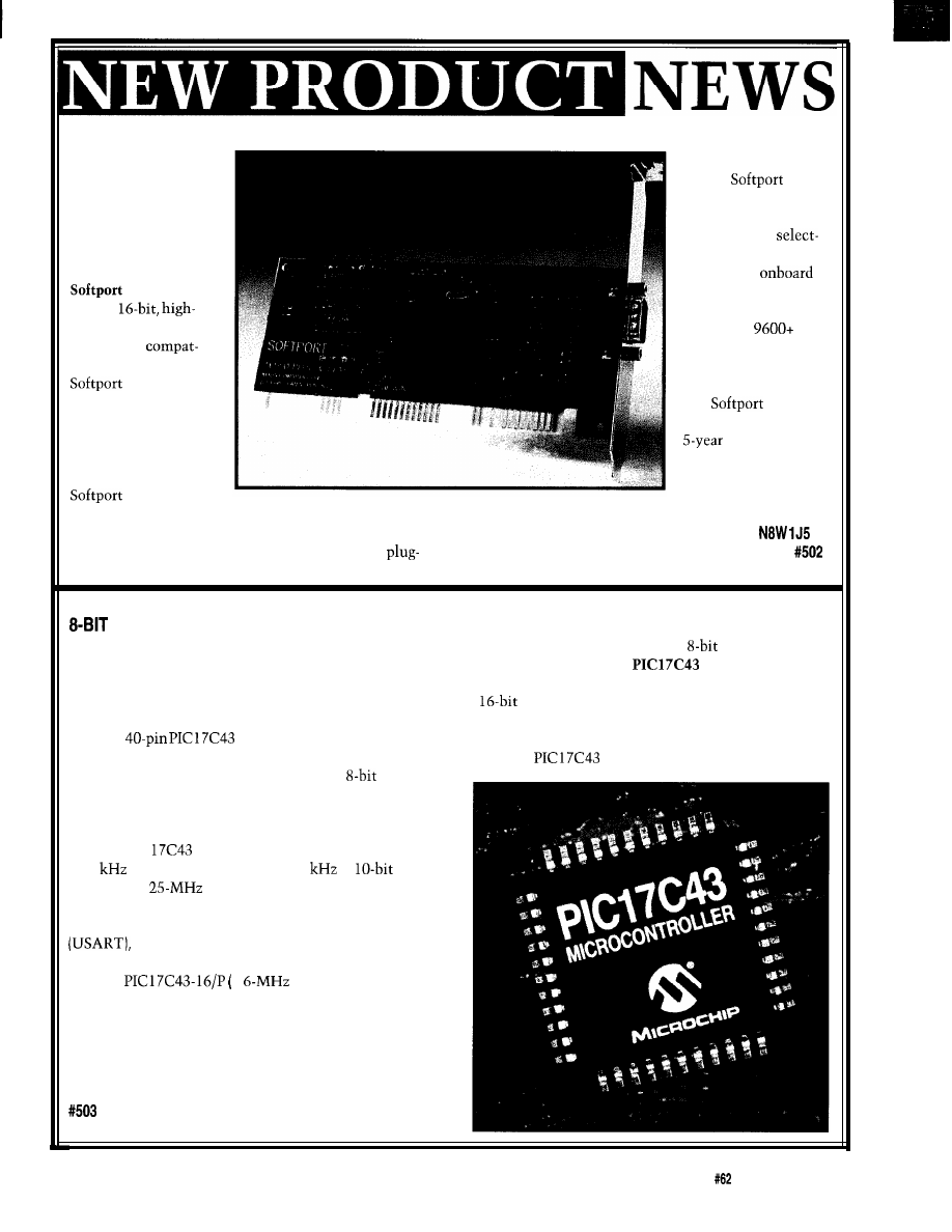
PLUG-AND-PLAY
SERIAL PORT
and-play environ-
ments,
A plug-and-play
automatically
serial port for IBM and
configures without
compatible computers
conflict when
has been introduced
ing I/O address and
by Axxon Computer.
IRQ for the
provides a
16550 UART. The
single,
high-speed serial port
speed 16550 serial
is ideal for
bps
port that is
external modems,
ible with Windows 95.
pointing devices, or
is completely
fast data transfer.
free of jumpers for
sells for
configuration in both
$69 and comes with a
plug-and-play and
warranty.
Legacy environments
(non-plug and play).
functions in
either S-bit or 16-bit ISA or EISA slots.
Axxon Computer Corp.
Included software can change the serial port address
3979 Tecumseh Rd. East
l
Windsor, ON
l
Canada
and select from interrupts 3-7, 9-12, or 15. With
(519) 974-0163
l
Fax: (519) 974-0165
OTP MICROCONTROLLER
Microchip Technology has introduced a high-performance, one-time-programmable (OTP),
RISC
microcontroller that provides an instruction execution speed of 160 ns at 25 MHz. The
offers unique
execution of its two 8 x 8 unsigned hardware multiply instructions in a single instruction cycle. The fast execution
throughput offers a cost-effective alternative to more expensive
microcontrollers and dedicated digital signal
processors for certain math-intensive applications.
The
offers 4K x 16 OTP on-chip EPROM program memory and 454 bytes of user RAM for
longer and more complex software algorithms. These features make the
ideal for demanding real-time
embedded control applications where high
perfor-
mance is critical. Applications include industrial process
control, manufacturing equipment, motor control, robotics,
appliances, security systems, and data loggers.
The PIC
features include two PWM outputs of
97.7
at S-bit resolution and 24.4
at
resolu-
tion (for the
device) to enable more precise control
of process functions. Two fast-capture inputs with resolu-
tion of up to 160 ns, a fast full-featured serial interface
and a watchdog timer with on-chip RC oscillator
are also included.
The
1
version in a plastic DIP
package) is priced at $9.40 in quantity.
Microchip Technology, Inc.
2355 West Chandler Blvd.
l
Chandler, AZ 85224-6199
(602) 786-7200
l
Fax: (602) 899-9210
Circuit Cellar INK
Issue
September 1995
9
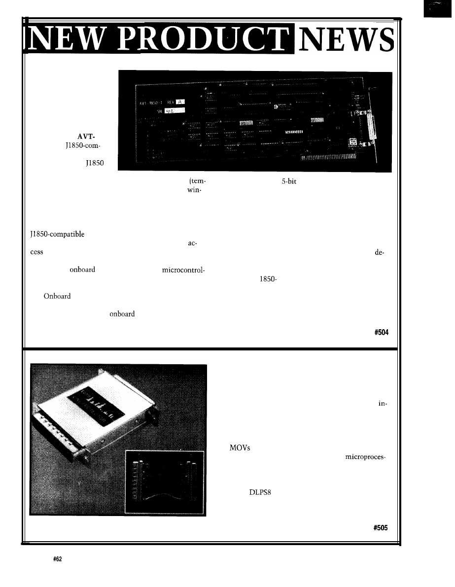
IN-VEHICLE
MULTIPLEX BUS
DEVELOPMENT
Advanced Vehicle
Technologies introduces
a development platform
for automotive-based
networks. The
1850-l
is a
pliant system for IBM PC
compatibles. SAE
is a two-part standard for
in-vehicle multiplex buses. These buses let sensors
include S-bit parallel,
parallel, serial peripheral
perature, pressure, speed, torque), actuators (locks,
interface (SPI), as well as controller interrupt and status
dows, etc.], and controllers communicate. External test
lines. Combined with internal timer and I/O functions,
equipment can also access the bus for diagnostics and
these interfaces offer a wide variety of functions and
maintenance.
integration with nearly any sensor, actuator, and so on.
The AVT- 1850-l reduces the risk in developing
The software is an integrated environment that
nodes. Designed to be used with a PC,
implements and debugs node and network software on
the board and software give a developer immediate
one platform. Called the
Enhanced On-Line Software
to the target hardware and interfaces. The board has
(EOS), it consists of program development, program
all network-interface functions controlled by a Harris
bugging, and network monitoring. EOS requires DOS 5.0
HIP 7030A0
microcontroller. The
or higher. A Windows version will be available by year end.
ler off-loads from the host processor all network-related
The AVT-
1 Development Package sells for
activity, thus freeing the host.
$1500 and includes telephone technical support and
dual-port memory is mapped into the host
software upgrades for one year.
computer’s memory space, so the user can control and
view the operation of the
microcontroller. All
Advanced Vehicle Technologies, Inc.
interfaces with the HIP 7030A0 are accessible to the
1509 Manor View Rd.
l
Davidsonville, MD 21035
designer via a rear-panel connector. These interfaces
(410) 798-4038
l
Fax: (410) 798-4308
DATA-LINE SURGE SUPPRESSOR
Data communication lines are susceptible to electri-
cal disturbances and surges. In particular, the RS-232
serial port is vulnerable to damage resulting in burnt or
damaged cards or motherboards. L-corn is offering an
line device to act as a permanent safeguard.
Model DLPSS
features silicon avalanche zener di-
odes on eight data lines (pins 2-8 and 20) to protect
against transient voltages. Avalanche diodes react faster
than
and are voltage sensitive to provide a more
accurate 27-V threshold level for sensitive
sing circuits. The power-handling capability is 600 W on
each line. The device features an all-metal case with
male and female connectors for in-line operation.
Model
sells for $28.95 in single quantities.
L-corn
1755 Osgood St.
l
North Andover, MA 01845-1092
(508) 682-6936
l
Fax: (508) 689-9484
10
Issue
September 1995
Circuit Cellar INK
FEATURES
Developing an
Engine Control System
Ed Lansinger
Em bedded
Debugging Tricks
Designing an
grade XYZ Router Table
Developing an Engine
Control System
Part 1: System Architecture
and Fuel Delivery
campus in a race car
might get suspended at
most schools. But, at Rensselaer Poly-
technic Institute, such frivolity can
earn you course credit, especially if
that race car features a
engine control system.
This article is the first in a
part series describing the system I
developed as a senior project. After
explaining system requirements, I’ll
diagram the system architecture and
delve into its fuel-delivery subsystem.
The two subsequent articles deal
with the ignition subsystem, other
interface electronics, the code required
to tie everything together, and testing
and tuning the system. Ultimately, I’ll
cover the complete system: hardware,
software, sensors, actuators, installa-
tion, and testing.
After finishing the series, I hope
you will be able to duplicate this sys-
tem for your own applications.
REQUIREMENTS
The Engine Control Module
(ECM) was developed for Formula SAE,
an intercollegiate competition spon-
sored by the Society of Automotive
Engineers and the Big Three
12
Issue
September 1995
Circuit Cellar INK
makers. Over 70 colleges
across North America par-
ticipate, each school build-
ing a single-seat, open-wheel
race car from scratch. The
cars are raced in an annual
competition held in Detroit.
Competition is fierce. Every-
one is looking for an edge,
the rules encouraging the
development of advanced
technology.
driveability than a carburetor, be easier
to tune, and gain a base for future
advanced control systems.
Carburetors had given
us poor performance, so we
chose a fuel-injection sys-
tem to get a performance
advantage. I developed the
ECM to optimize
power output, provide better
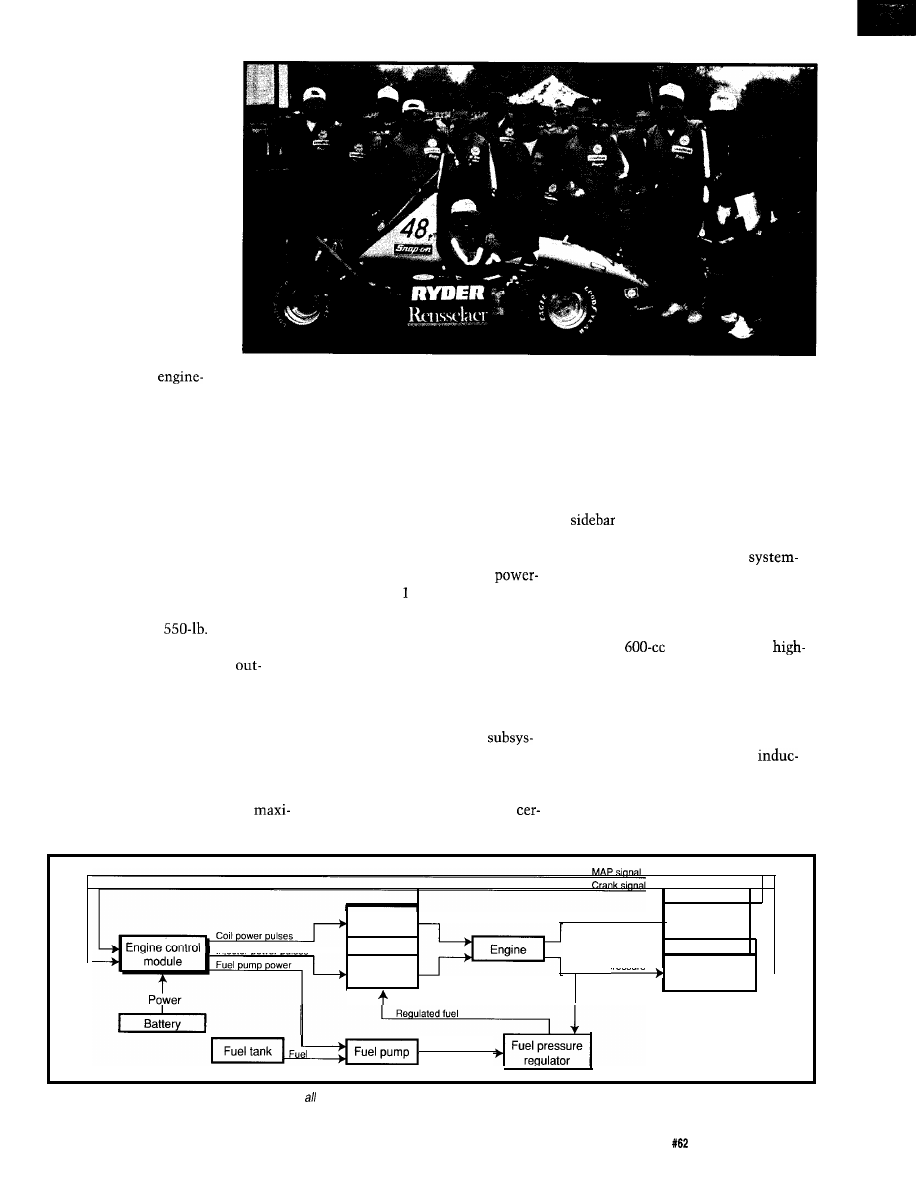
Photo l--Students on the 1994 Rensselaer Formula SAE Team used a fuel injection system they developed from scratch to race
in a national competition. The author is standing directly behind fhe person seated in the car.
Fundamentally, the ECM needs to
do just two things:
l
provide the correct amount of fuel to
the engine
l
fire spark plugs at the right time.
It sounds simple enough, but think of
the environment in which the ECM
must operate. Our
car with a
70-hp engine is made of composites
and chrome-moly steel. It can
accelerate, out-brake, and out-corner
nearly all production automobiles. The
g-forces, vibration, and shock leave
drivers breathless and fatigued after
only
15
minutes.
tern. But, by having these figures now,
one end of the crankshaft. An
Now, consider that the ECM has
you’ll get the big picture up front.
tive sensor generates pulses as the
to ride shotgun for countless hours of
Central to the proper operation of
leading and trailing edges of these
testing and racing. It must wring
the ECM is the requirement that
teeth rotate past. Engine position and
mum power out of the engine at the
tain actions happen at the right time
speed are determined from this signal.
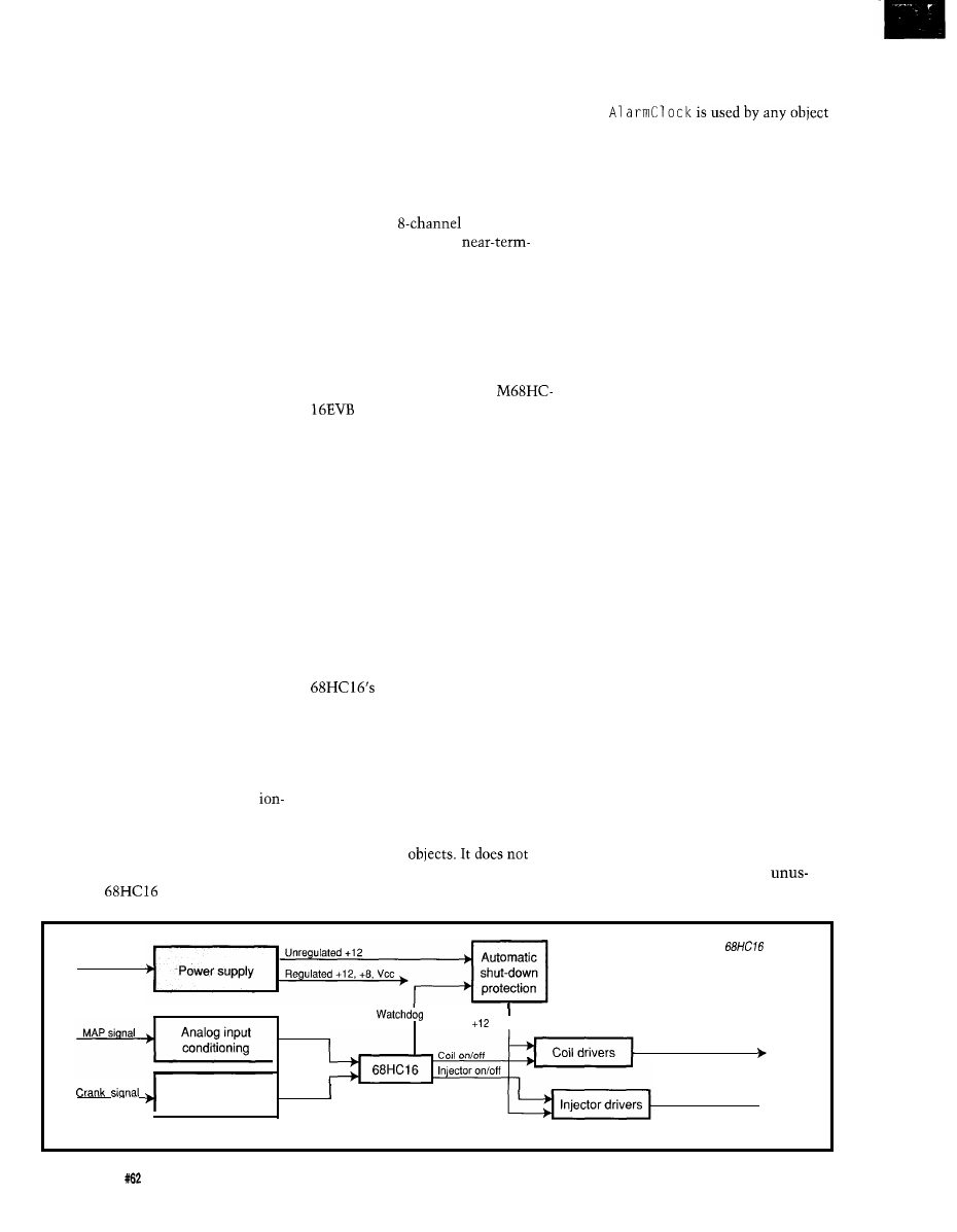
The block diagram of the
train in Figure includes the ECM.
The ECM is a microcontroller with
interface electronics and control soft-
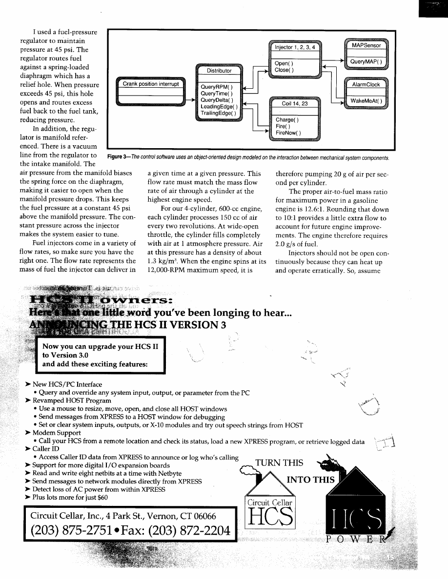
ware. Figure 2 takes a look at the hard-
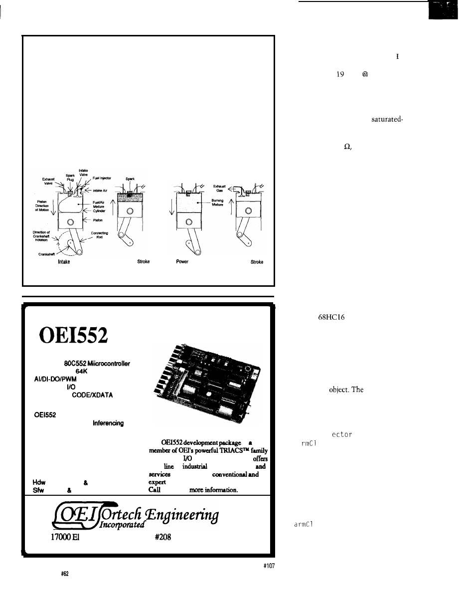
ware inside the ECM, while Figure 3
depicts the software architecture run-
ning on the micro. As this series
progresses, I’ll cover the items in these
figures with their respective
Early on, I made several
design decisions based on the hardware
available to me, competition rules,
experience, and preferences. Here are
the most important.
The
engine is from a
performance motorcycle. It has four
cylinders, a crank-position sensor, and
no distributor. Four teeth, one long
and three short, are cast into the
engine’s flywheel, which is attached to
driver’s command. When possible, it
must protect the engine and the driver
Furthermore, it must remain in
control at all times, even with RF
from dangerous conditions.
ignition noise so severe it can reset a
CPU.
ARCHITECTURE
relative to the position of the pistons
and valves within the engine. I refer
frequently to the four strokes: intake,
compression, power, and exhaust. It is
important that you understand what
goes on during each stroke (read the
on the four-stroke engine if
you need an update).
Ignition
Sparks
Crankshaft rotation
Crank position
coils
sensor
Injector power pulses
Fuel
Intake air pressure
Manifold
injectors
Fuel pulses
pressure sensor
Pressurized fuel
Figure l--The Engine Control Module relies on inputs from over the engine for making control decisions.
Circuit Cellar INK
Issue
September 1995
13
Injection is by a technique known
as simultaneous double fire, in which
injectors fire in pairs once per revolu-
tion. This technique differs from a
sequential setup that individually fires
injectors every other revolution ac-
cording to when the intake valve
opens. While the latter technique gives
greater control over fuel delivery, it
requires an additional sensor to detect
the camshaft position. The differences
between the two disappear at high
RPM, which is the operating region of
concern for a race car.
To determine the correct amount
of fuel to inject, I decided to use a
speed-density system. Such a system
uses two inputs to determine fuel
flow: RPM and air pressure inside the
intake manifold. RPM is calculated
from the crank-position signal. Air
pressure is measured by a manifold
pressure sensor, otherwise known as a
MAP sensor. I used an automotive
MAP sensor which generates a 0-5-V
output proportional to air pressure. A
vacuum line runs from the intake
manifold to the sensor.
Since the engine had no distribu-
tor, I used two ignition coils, each
firing two plugs at the same time. This
method works because one cylinder
fires on the compression stroke while
its twin fires on the exhaust stroke.
Dual firing does no harm because a
spark fires in the exhaust cylinder
when there is nothing left to burn.
There is little decrease in spark energy
fast and was developed in conjunction
with an automobile manufacturer
specifically for this type of application.
The chip has built-in output-com-
pare timers, so actuators can be con-
trolled by a hardware time reference. It
also has input capture timers that
timestamp an input edge and cause an
interrupt. An
A/D converter
handles all current and
future analog-input requirements.
A Background Debug mode gives
greater control and flexibility during
debugging. Other features, such as
access to lots of memory, queued serial
communications, and DSP instruc-
tions, are there for future expansion.
The ECM uses the Motorola
evaluation board, which I found
to be an excellent development tool. It
comes with a very useful assembler,
debugger, and simulator.
The code is in assembly. Because
the system deals with physical objects
that interact in well-defined ways, I
chose an object-oriented approach.
Achieving a clean design for the code
was aided by using the physical system
as a model for the software objects and
the messages they send.
The impact of the overhead to
support objects in assembler was insig-
nificant, especially in light of the
speed and address space.
Actual processing time is only a small
fraction of available CPU time, even at
the highest engine speeds.
Two important objects in Figure 3
distributors present on some types of
engines.
wishing to be sent a wake-up call at a
certain time in the future from a few
dozen microseconds to hours. These
two objects are the autonomous ner-
vous system keeping the ECM alive.
FUEL DELIVERY HARDWARE
Fuel is delivered by the fuel pump
through a pressure regulator to the
injectors, which are controlled by the
ECM. A fuel injector is an on/off sole-
noid valve that gates pressurized fuel
from the fuel rail into the intake mani-
fold.
When the injector is opened, it
sprays a mist of fuel at a constant flow
rate. Each revolution, an injector is
pulsed on for a short period of time.
The duration of this pulse is termed
injector pulse width.
The width of the
pulse determines the total amount of
fuel injected per revolution and must
be carefully matched to current operat-
ing conditions.
All this subsytem’s mechanical
elements up to the injectors are re-
sponsible for delivering a supply of
clean fuel at sufficient pressure. I
chose a high-pressure fuel system
where the fuel is pressurized by an
electric fuel pump before being sent to
the injectors. A variety of OEM and
aftermarket fuel-injection components
are available for high-pressure systems.
The electric fuel pump runs on 12
available to the compressing cylinder
require a bit of explanation before
V and draws about 8 A. It is mounted
because the hot exhaust gases are
moving on. The
Distributor is
outside the fuel tank with an in-line
ized and add very little resistance to
driven by the crank-position signal and
fuel filter between it and the tank.
the spark current path.
schedules the operation of the Co i 1
This filter is absolutely essential. The
Several microcontrollers would
a n d
I n j e c t o r
smallest amount of grit can seize an
work for this application.
I
chose the
represent a physical device, but its
electric fuel pump, making it
Motorola
because it is quite
operation is similar to the mechanical
able.
Power
Crankshaft position
signal conditioning
Figure P-Motorola’s
microcontroller provides the computa-
tional horsepower for the race car.
MAP
signal
high current
Coil power pulses
E d g e s
Injector power pulses
14
Issue
September 1995
Circuit Cellar INK
The Four-Stroke Engine
On the intake stroke, fuel and air are drawn into the cylinder. During
the compression stroke, this mixture is compressed. Shortly before the
piston reaches the top of the cylinder, the spark plug ignites the mixture.
The pressure caused by the burning mixture forces the piston down-
ward on the power stroke. This turns the crankshaft and delivers power to
the wheels. During the other strokes, momentum or another cylinder
keeps the crankshaft turning.
The spent exhaust gas is pushed out of the cylinder on the exhaust
stroke, and the cycle repeats.
The sequence can be conveniently remembered as “suck, squish, pop,
ptooey.”
Stroke
Compression
Stroke
Exhaust
NEW 8051 Family Development System
with
Fuzzy Logic Support
DX126 Control Board
l
Powerful
l
Memory up to
ROM/
32K
RAM
l
Signal Conditioning
l
Expansion
Header
l
Configurable
Overlays
Software Features
l
Monitor/Debugger
l
FL1552 Fuzzy Logic
Engine
l
DGU552 Diagnostic Package
This is Not a Toy!
l
Fuzzy Logic Control Template
l
Numerous Implementation Examples
The
is
Also Available
of industrial control modules. OEI
l
Fuzzy Logic Development Tools
a full
of
control products
l
Software Development Tools
utilizing both
l
Accessories Add-on Modules
system technology.
l
Drivers Control Packages
today for
Camino
Real, Suite
l
Houston, TX 77058
Phone: (713) 480-8904
l
Fax: (713) 480-8906
16
Issue
September
1995
Circuit Cellar INK
that the injector operates at a maxi-
mum 80% duty cycle. Therefore, the
fuel flow rate must be about 2.5 g/s.
chose commonly available automotive
injectors rated at lb./h 45 psi,
which is 2.4 g/s. A larger injector could
be used, but one that is too large has
trouble metering small quantities of
fuel and the engine cannot idle well.
The injector I chose is a
circuit type, designed to be switched
by a transistor directly to 12 V. The
coil resistance is
12 so
the drive
current through the transistor is only
about 1 A.
There are power Darlington driv-
ers in a DIP package that can be used
for driving this type of load. However,
these may not have the power-dissipa-
tion capacity to handle all four injec-
tors being on simultaneously.
For this reason, I chose discrete
TIP120 power Darlingtons. They easily
handle the current, are not damaged by
the inductive-voltage kick when the
injector closes, and require only mini-
mal heatsinking (a 1” square area of
copper on the board does just fine].
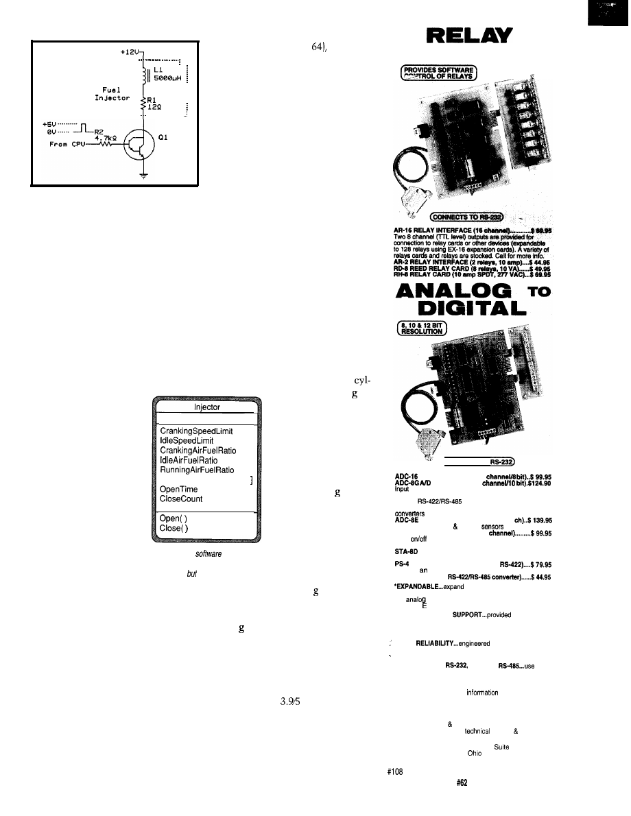
Figure 4 shows how simple the
drive circuit is. Turning an injector on
and off is a simple matter of turning on
and off the
output it’s con-
nected to.
ALGORITHMS AND SOFTWARE
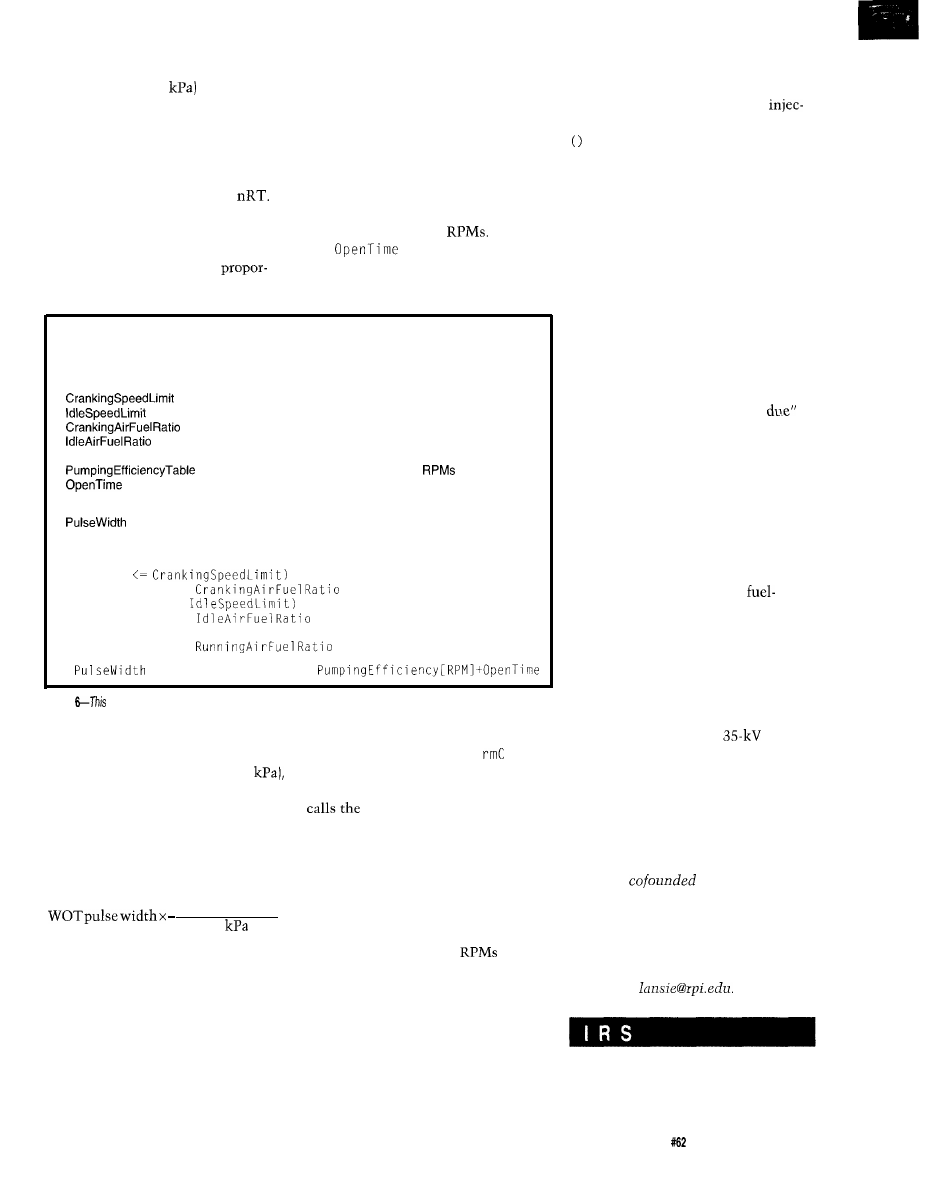
Figure 5 shows the data members
and messages for the I n j e c t o r class.
An I n j e c t o r object receives the
Injector.OpenO messagefromthe
Distributor
Injector
object looks at current operating con-
ditions and determines a correct pulse
width. Having turned on the physical
injector and calculated the pulse
width, the In j
object tells the
Al a
oc
k object to send it an
Injector.CloseO messageafterthe
required time period elapses.
Note that the injectors are not
directly controlled by a hardware timer
since there are not enough output
compares for individual injector actua-
tion. Of the five available, two are
used for the ignition coils and one by
Al
ock, both of which have more
stringent timing requirements.
One solution pairs the injectors by
driving two off the same transistor.
. . . . . . . . . . . . . . . . . . . .
T I P 1 2 0
Figure
4-The injector drive circuit makes turning the
injector on
and off as simple as flipping a processor
output bit.
In this speed-density system, fuel
required by the engine is a function of
manifold pressure and RPM. Ideally,
the engine is run on a dynamometer
and all combinations of pressure and
RPM are tested for each combination
of pulse width that results in maxi-
mum power. If reasonable limits on
quantization are made, say 32 steps
between full vacuum and atmospheric
pressure and O-12,000 RPM in incre-
ments of 500 RPM, one ends up with
32 x 24 = 768 points to test.
This solution, however, precludes
adjusting individual injector pulse
widths to account for differences in air
flow between cylinders. It turns out
that the off messages generally do get
sent on time. Even if they are slightly
off, they err on the late side, providing
slightly more fuel than necessary,
which is safer than feeding too little.
There are a few important things
to keep in mind when creating a fuel-
ing algorithm. First of all, running an
engine for too long with
insufficient fuel can melt
internal engine parts.
“Too long” is dependent
on the engine and condi-
tions, but can be as little
as several seconds. If an
error in fueling is made,
it must be the sort of
error that doesn’t last
very long or result in too
much fuel.
Such testing can take a lot of time.
I knew from previous tests that at
wide-open throttle (WOT), the injector
pulse width is fairly constant, regard-
less of RPM. I therefore chose to base
the injector pulse width solely on pres-
sure. I recorded pulse width at WOT
and used the ideal gas law to estimate
pulse width at lower pressures.
A good initial guess at WOT pulse
width can be made from the estimated
air flow through the engine. Each
PumpingEfficiencyTable[
Figure
5-The
model for a
mechanical fuel injector includes
lots of data, on/y two message
functions.
Still, too much fuel
causes power reduction
and carbon fouling of the
spark plugs. In the worst
case, the injectors open
and never shut off, filling
the cylinder. Not only can this cause
fuel to leak out of the engine, creating
a fire hazard, but if the engine is spun,
it tries to compress a cylinder full of
liquid fuel, which breaks internal
parts. If you are lucky enough not to
break anything, you must still change
the oil immediately since it will likely
be full of fuel and useless as a lubri-
cant.
rate of 2.4 g/s, so the flow time for
0.0080 is 3.3 ms.
Since the injectors need 0.6 ms to
open, a total pulse width of 3.9 ms is
needed. As a quick check on injector
size, note that one revolution at 12,000
RPM takes 5 ms. Thus, our injectors
operate at a safe
= 78% duty cycle
while providing the right amount of
fuel at maximum RPM.
My system was protected by a
separate automatic shut-down circuit
Part-throttle pulse width can be
extrapolated knowing the manifold
(to be described in INK
which
prevents fuel overflowing through
software glitches.
inder draws in 0.2 of
air per intake stroke at
WOT. As mentioned,
maximum power occurs
with an air-to-fuel mass
(not volume) ratio of
12.6: 1. So, for each
intake stroke, we need
to inject 0.016 of fuel.
Note that one in-
take stroke occurs every
two revolutions, and
the injectors are pro-
grammed to fire once
per revolution. We need
two separate injections
of 0.0080 of fuel. The
injectors have a flow
INTERFACE
(CONNECTS TO
A/D CONVERTER’ (16
CONVERTER’ (6
voltage, amperage, pressure, energy usage,
joysticks and a wide variety of other types of analog
signals.
available (lengths to 4,000’).
Call for info on other AA configurations and 12 bit
(terminal block and cable sold separately).
TEMPERATURE INTERFACE’ (6
Includes term. block 6 temp.
(-40’ to 148’ F).
STA-6 DIGITAL INTERFACE’(6
Input
status of relays, switches, HVAC equipment,
security devices, smoke detectors, and other devices.
TOUCH TONE INTERFACE’................ $ 134.96
Allows callers to select control functions from any phone.
PORT SELECTOR (4 channels
Converts
RS-232
port
into 4 selectable RS-422 ports.
CO-465 (RS-232 to
your interface to control and
monitor up to 512 relays, up to 578 digital inputs, up to
128
the PS-4.
inputs or up to 128 temperature inputs using
X-18, ST-32 &AD-18 expansion cards.
FULL TECHNICAL
over the
telephone by our staff. Technical reference&disk
including test software&programming examples in
Basic, C and assembly are provided with each order.
HIGH
for continuous 24
hour industrial applications with 10 years of proven
performance in the energy management field.
CONNECTS TO
RS-422 or
with
IBM and compatibles, Mac and most computers. All
standard baud rates and protocols (50 to 19,200 baud).
Use our 800 number to order FREE INFORMATION
PACKET. Technical
(814) 484.4470.
24 HOUR ORDER LINE (800) 842-7714
Visa-Mastercard-American Express-COD
International Domestic FAX (814) 484-9658
Use for information,
support orders.
ELECTRONIC ENERGY CONTROL, INC.
380 South Fifth Street,
804
Columbus,
43215.5438
Circuit Cellar INK
Issue
September 1995
17
pressure. The pressure in the manifold
is atmospheric
(100
at WOT. As
the throttle blade closes, it restricts
the amount of air flowing into the
intake manifold, reducing the mani-
fold pressure.
Remember from high-school phys-
ics the ideal gas equation PV =
From this equation, you can derive a
formula that shows that for a given
volume and temperature, the mass of
air in the volume is directly
The computed pulse width is
multiplied by a factor of O-2 depending
on RPM. This factor is looked up in a
pumping-efficiency table. The airflow
through most engines varies somewhat
at different engine speeds due to reso-
nances in the manifolds and flow re-
strictions. This table allows the pulse
width to correct for changes in airflow
that occur at different
is
added as the last
step. The code first computes the total
tional to the measured pressure.
time that the output signal to the
Inputs:
MAP
current manifold pressure
RPM
current engine speed
Calibrations:
RPM below which the engine is considered to be cranking
RPM below which the engine is considered to be idling
constant that determines air/fuel ratio at cranking speeds
constant that determines air/fuel ratio at idle speeds
RunningAirFuelRatio
constant that determines the air/fuel ratio at running speeds
table of pumping efficiencies at different
time it takes for injector to open
outputs:
length of time the injector must be open over the next
engine revolution
Equations:
if (RPM
AirFuelRatio =
else if (RPM <=
AirFuelRatio =
else
AirFuelRatio =
= AirFuelRatio x MAP x
Figure
algorithm runs once per revolution for each injector to determine how much fuel should be injected.
As a reasonable approximation
then, if the manifold pressure drops to
half of what it is at WOT (i.e., 50
the mass of air entering the cylinders
is also cut in half. The required fuel
mass and injector pulse width is simi-
larly cut in half. So, knowing the WOT
injector pulse width, the pulse width
for any operating condition is simply:
manifoldpressure
100
At idle, when there is no need to
produce maximum power, I can save
fuel by using a different pulse width
based on a 14.7: 1 air-to-fuel ratio, the
ratio for best fuel economy. I also need
a richer mixture during cranking to
make starting easier. In the code, I
therefore chose different base pulse
widths depending on RPM.
injector should stay high. It then turns
the injector on and tells A
1
a
1 o c
k
to
send a turn-off message at the right
time in the future. This command
Injector.CloseO function
at the appointed time. Figure 6 speci-
fies the injector-pulse-width computa-
tion.
Next month, I’ll show you how to
generate carefully timed
sparks
without frying any electronics or send-
ing the CPU out to lunch with RF
noise.
q
Under certain rare conditions, the
possibility exists that the injector
might not close before it needs to be
opened again. This problem is most
likely to happen at high
at
WOT. Theoretically, with a properly
sized injector, this should never hap-
pen, but software latencies or an erro-
neous pulse-width calibration could
cause it.
Ed Lansinger is a computer and
systems engineer who worked on the
Cadillac Northstar powertrain control
software,
an industrial
software company, and does consult-
ing. He has returned to Rensselaer
Polytechnic Institute for graduate
studies and is forming a team there to
build an electric race car. He may be
reached at
So, I implemented a counter that
401 Very Useful
increments every time the injector is
402 Moderately Useful
reopened, even if it is already open.
403 Not Useful
The counter represents the number of
extant Injector.CloseO messages
waiting to be processed for that
tor.Eachcallto Injector. Close
decrements the counter, and only
when it reaches zero is the injector
actually turned off.
When pulses overlap in this fash-
ion, the later pulses are shortchanged
by this scheme since the total amount
of injected fuel is less by the amount
of overlap than the sum of the indi-
vidually scheduled pulses. This is not
a condition to be concerned about
since the open times for each pulse
become full-flow times since the injec-
tor is already open. Also, every other
revolution, all the fuel is flushed
through the cylinder, so there is no
point in trying to inject a “past
amount of fuel.
Since this condition happens
rarely and lasts only briefly, it does not
harm the engine.
CONCLUSION
The development of electronic
fuel injection paved the way for in-
creased vehicle performance while
meeting strict emission and
economy requirements. It made our
race car more powerful and easier to
drive. It’s a far cry from the earliest
attempts at mixing fuel and air, one of
my favorites being the use of a wick
just like a kerosene lamp!
Circuit Cellar INK
Issue
September 1995
19

Embedded
Debugging
Tricks
Stuart Ball
problem we’ve
all encountered in
working with
embedded microproces-
sors is debugging the pesky things.
Our equipment sometimes must
be debugged at a customer site without
affecting customer operations. This
situation often precludes the use of an
emulator where the processor stops
when a breakpoint is detected.
In some cases, no emulator is
available for the processor. Conse-
quently, I cannot
pin connector (see Figure 1). This con-
nector contains a ground, write strobe
l
STB), and eight data lines (DO-D7). I
usually implement the connector as an
header. The microproces-
sor being debugged contains in firm-
ware instructions that write specific
data to the test connector so it can be
captured and analyzed. Figure 2 shows
the timing of the write operation.
For example, Table offers a par-
tial list of values (in hex) that
I
used on
a recent character-recognition project,
implemented with a DSP. Each time
the DSP enters the A/D converter’s
sampling routine, it outputs a value of
02 to the test port. A detection of a
character edge produces 03.
Using a logic analyzer (in state
mode) connected to the standard test
connector, I can trace the history of
program operation by time tagging the
data. Of course, with the proper inter-
face, the data could just as easily be
transmitted to and logged on a PC.
On this DSP system (see Figure
the write strobe for the standard test
ways depend on an
emulator.
It is also critical
that the debug data be
generated from the
1 2
Gnd
DO
D3 D4
D6 D7
Figure l--By including a standard
in every new design, if’s
possible develop a common set of test fools
can be used on all
normal operating code.
d e s i g n s .
I cannot use a method
requiring a handshake with a host PC
or terminal. The system can’t behave
one way when a debugging tool is
connected and another when it is not.
Over my fifteen years as an elec-
trical engineer working with embed-
ded microcontrollers, microprocessors,
and
I’ve developed a standard
debugging technique I’d like to share
with you.
MY TECHNIQUE
The basic debugging system I have
developed makes use of a standard
*STB
D o - D 7
Debug data
Figure
test-connector signal
requirement is
be stable on rising
edge of
connector is just another address de-
code line from the PLD already on the
board for the other DSP peripherals.
The data lines on the standard test
connector are the DSP data lines. On a
or x86 family processor, the write
strobe can be a spare memory or I/O
decode. On a Motorola processor with-
out a separate I/O space, the strobe
must be a memory decode.
This technique works fine if you
have decoded read/write strobes for
peripherals connected to the CPU.
However, I don’t always have the
luxury of a spare I/O line, and some-
times I don’t have any I/O decoding at
all. Nevertheless, I still like to use the
standard connector for debugging.
Figure shows a generic debug-
ging system. The microprocessor in
the system under test outputs test
values to a debug output circuit. They
are translated to the standard output
20
Issue
September 1995
Circuit Cellar INK
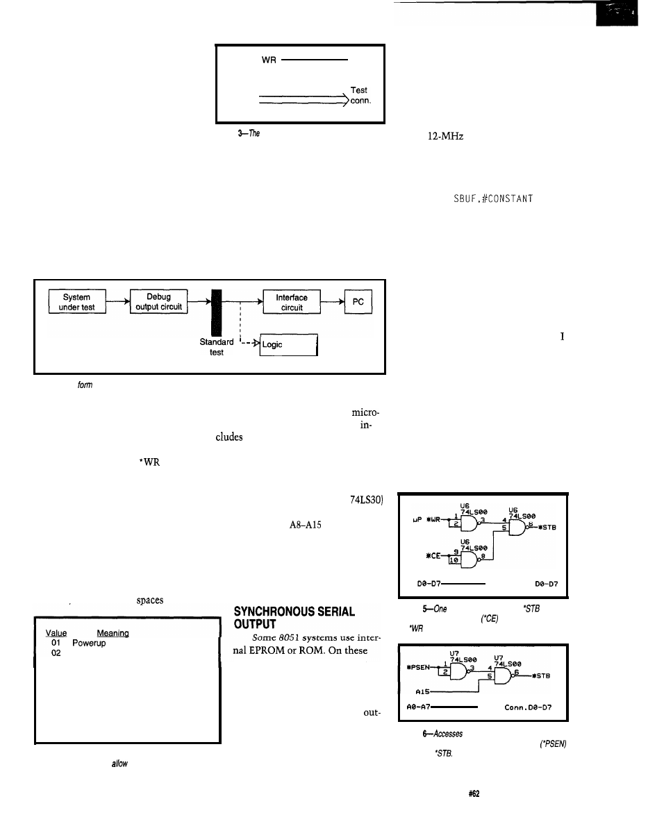
connector format and can then be
captured by a logic analyzer or trans-
mitted to a PC.
On systems, such as this DSP
system, the debug output circuit
merely connects the data lines and
decoded strobe to the test connector.
On others, the circuit is more com-
plex, requiring approaches like the
ones below.
WRITE TO ROM
Most micros use an external ROM
or EPROM. Normally, there is nothing
else residing in the EPROM address
space. If a write is executed to the
EPROM space, the data won’t go any-
where, but it can still be captured with
Decoded
‘STB
from address
decode logic
DO-D7
DO-D7
Figure
debugger uses
generic connections
from a microprocessor to the standard test connector.
often separate, so you can’t write to
the EPROM. However, they can read
data from the EPROM. The circuit in
Figure 6 is based on the fact that most
8051 systems (at least most of mine)
don’t use the entire 64-KB space. Any
access to the upper 32 KB (Al5 = 1)
generates the l STB signal. In this case,
analyzer
connector
Figure
4-The
the debug output circuit takes depends on the system under test, but everything from the test
connector on can be identical no matter what system is being checked.
the simple address decoding logic of
The test connector data lines connect
to those of the microprocessor.
Figure 5. This circuit generates the
l
STB signal with a 74LSO0. The l CE
signal to the EPROM (pin 20 on a
27256) is gated with the
signal.
This method works with any mi-
cro that has an external EPROM and
can write to the EPROM address space.
Some micros require more logic to
decode the strobe.
READ EPROM ADDRESS
space is unused and is discarded. If you
need more than 32 KB of EPROM, use
the debug data comes from the
a wider NAND gate [such as a
processor address lines. Listing 1
and decode the address lines to gener-
ate l STB when
are all ones.
This technique uses the upper 256
the code which implements
bytes (FFOO-FFFF) for the debug space,
leaving the remainder for code.
this on an 805 1.
The value read from the EPROM
On 805 1 systems with external
EPROM. code and data
are
Of course, this method works for
most micros with an external EPROM.
reset processing complete
ADC sampling interrupt entry
03 Character edge detected
systems, generating debug data
04 Blanking on
1 x
Character recognized;
x = char code (O-F)
2 x
Host command received;
x = command code (O-7)
with the 8051 serial output con-
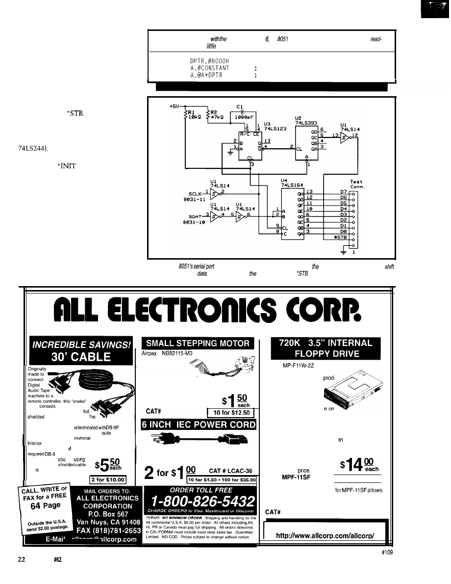
nected to the COM port of a PC is
common. The circuit in Figure 7,
however, uses the 8051 serial
3 x
Recognition occurred when blanking;
x =
char code (O-F)
put in synchronous mode.
This method provides two
Table
l--Data values sent to the debug output represent
various program states to
tracing.
advantages over the asynchronous
mode:
l
you can use a standard test connec-
tor
l
the maximum rate of debug output
data increases
When programmed for synchronous
mode, the 8051 outputs data at 1 Mbps
with a
input clock. Still, this
method limits the maximum output
data rate. The output code for this
method is:
MOV
This debug method has the advan-
tage that no CPU registers are required
to output the data. The output instruc-
tion can be put anywhere in the code
without having to verify that a needed
register hasn’t changed.
However, it is possible to output
data to the serial port faster than it can
be transmitted, which results in gar-
bage values. When I use this method,
don’t put the debug circuit on the 805 1
board. Instead, I use a separate bread-
board and connect it to the 8051 via an
IC clip.
USING DEBUG DATA
Generating debug data is useless if
you can’t do anything with it.
Figure 8 shows a FIFO connected
to a PC parallel printer port. The FIFO
is written with data from the standard
ROM
T e s t C o r m .
Figure
alternative for generating
gates
the ROM chip select signal
with the microproces-
sor
signal.
T e s t
Figure
to ROM above 8000h are decoded
and gated with the microprocessor read signal
to generate
Debug data uses microprocessor
address fines.
Circuit Cellar INK
Issue
September 1955
21
test connector. When the FIFO has
data, the *ACK signal to the PC is
driven low. When the PC detects de-
bug data, it reverses the direction of
the port (you must use a bidirectional
port), then drives *STB low to read it.
The specific code for this depends
on your PC. However, you can use any
other input and output control lines
for l ACK and
If your cable from
the FIFO board to the PC is more than
a foot long, it’s wise to buffer the data
lines with a bus driver IC (such as a
This circuit needs a reset for
the FIFO, which can be connected
either to the
signal on the
printer port or to the circuit under test.
Another way to send data to a PC
is to connect an 8031 to the FIFO, and
transmit the data serially to the PC via
the 803
1
serial output. Although I’ve
never used this technique, it lets you
collect data with a standard communi-
cation program such as Procomm.
While the FIFO permits debug
data to be sent faster than the serial
data rate supports, the average debug
data rate cannot exceed the serial data
Listing l--When used
circuit in Figure
the
assembly code necessary to generate a
from-ROM strobe adds
overhead.
MOV
MOV
MOVC
CONSTANT is the debug value
Read the EPROM, generate strobe
Figure
7-The
in synchronous mode can be used to generate debug data and
l
STB. The
register captures serial
from the 8051, and counter generates
when 8 bits are received.
QUALITY PARTS
l
DISCOUNT PRICES
l
FAST SERVICE
l
HUGE SELECTION
#
12 Vdc, 65 ohm
stepper motor with
6 leads. 15 degree step
angle. 1” diameter x 0.5”
high. Mounting flange with holes on 1.25” cen-
ters. 0.08” (2mm) dia. X 0.2” long shaft. 0.27” dia.
pulley is press-it onto shaft. Great
for robotics and experimentation.
SMT-13
Sony #
Brand new 720 KB floppy
drives. Built for an OEM
cable
of four separate
9 conductor plus drain wire,
cables in one jacket.
T
conductors are stranded 24
AWG wire. Each
end
of each smaller cable
con-
nectors. The cable is well-made and
flexible
for Its size. Snake cable
0 D ‘is 0.52”
cable O.D. is
0.15”. The outer jacket can
be
slit and removed only the 9 conductor cable is
connectors Include thumbscrew
hold-downs If
are
multiconductor
this a great deal.
CAT# CBL-3
CATALOG
That’s right! 6 inch...Standard 3 prong grounded
male one end and 3 prong IEC receptacle on
other end. CSA listed. Large quantity available.
uct, these are, in every
way, compatible with
PC/XT/AT computers
except that the faceplate
is slightly larger than thos
exact replacements. The faceplate size on these is
4.04” X 1.23”. (Normal size is 4” X 1”). The face-
plate is removable and can be trimmed if desired.
In some cases it may work without trimming. Also,
we have found that, when used 5.25” bays with
the adapter kit below, the adapter can easily be
modified to accommodate the unit. Because of this
slight inconvenience, we are
selling these drives at an
incredibly low
CAT#
10 for $120.00
INSTALLATION KIT
for installation into 5.25” drive bays. Simply cut and
remove three plastic gussets to Install.
FDD-3.5 $3.50 each
Visit
Our World Wide Web Site...
Issue September 1995
Circuit Cellar INK
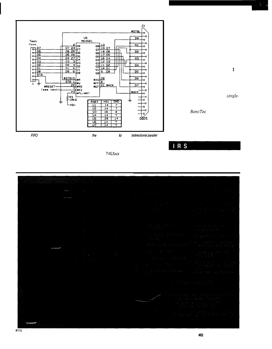
Figure 8-A
can be used as a buffer when connecting
circuit under test a PC’s
printer port.
rate or the FIFO overflows. You could
Of course, all of the logic shown
do the same thing with a discrete
here as
could be implemented
UART and some control logic, but the
with HC, AC/ACT, or as equations in
803 1 approach is probably simpler.
a PLD, the method I prefer.
MISSION ACCOMPLISHED
This standard debug connection
works with almost any microprocessor
or DSP system. It gives a window into
what the processor is doing with mini-
mal external connections. It can even
be used by factor-test technicians in
isolating faults.
It has saved me enormous time in
integrating and debugging circuits.
hope it does the same for you.
q
Stuart
Ball has spent the last 15 years
working on systems as diverse as
Global Positioning System and
chip interface translators. He is
currently employed as a principal
engineer at
Technologies, a
manufacturer of document processing
equipment for the banking industry.
He
may be reached
at
(405) 354-5042.
404
Very Useful
405 Moderately Useful
406 Not Useful
Circuit Cellar INK
Issue
September 1995
23
Designing an
grade XYZ
Router Table
advantages made me crave it for my
own woodworking projects. I decided
to develop a system of my own that
was as affordable and capable as the
expensive commercial units.
Aside from the satisfaction de-
rived from building things, my ulti-
mate goal was entrepreneurial. I was
approaching this project as a part-time
business venture and was concerned
about keeping costs under control.
With these guidelines in mind, I
began my largest project ever.
MECHANICAL ENGINEERING AND
CONSTRUCTION
From brochures, prices, and specs,
looked good on paper, I abandoned it
since it was going to be quite difficult
to build. I gave the toothed belt and
pulley scheme serious consideration,
but I had occasion to see an example of
an XY table using this approach. It
required significant speed reduction,
which would have made construction
more difficult.
At this point, a lead-screw system
looked attractive. The price of a
commercial lead screw and nut was
prohibitive. However, I discovered that
general-purpose thread rod is available
cheaply in 12’ lengths. Even though
these rods aren’t hardened, I decided to
use them and replace them as needed.
Since the threads on thread-rod are
rolled on, significant backlash occurs
in a combination of thread-rod lead
screw and nut. To eliminate the
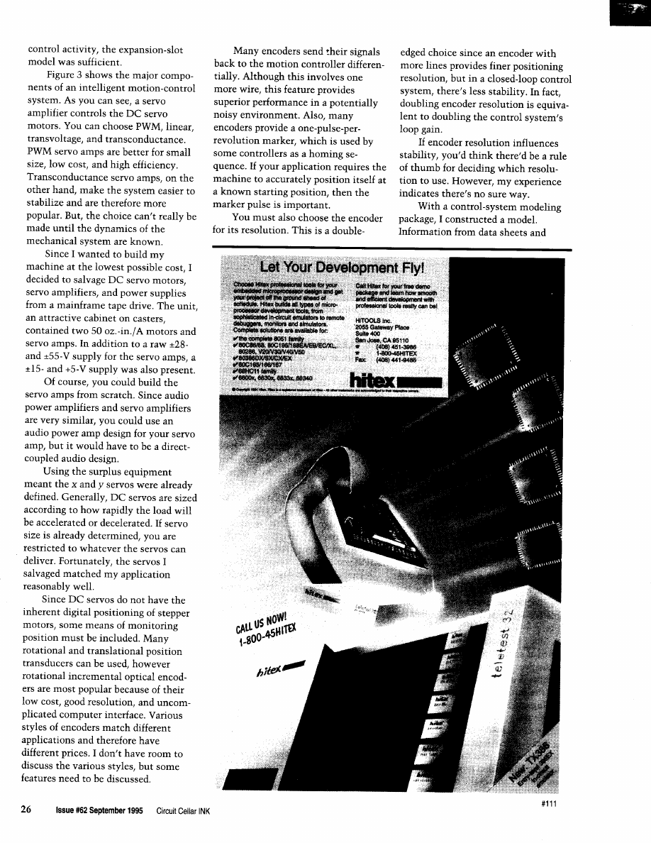
backlash, I used a double nut scheme
as shown in Figure
1.
Having the motors and their
sheet, I knew the armature moment of
inertia. I picked a lead-screw diameter
to suit this moment of inertia. Since
the lead screw and nut mechanical
advantage is so large, the movement of
the translational mass reflected back
down the motor shaft as a moment of
inertia is extremely small. Hence, it
has very little effect on the
of the motor. However, since
the lead screw attaches directly to the
two
trends were evident:
l
rotational-to-translational
sion uses a rack-and-pinion gear
l
motion stages use bearings on a
hardened steel rail.
Side view
End view
Figure
key to table
is fixed
that move along each axis of motion as lead screw onto which
they are threaded rotates.
24
Issue
September 1995
Circuit Cellar INK
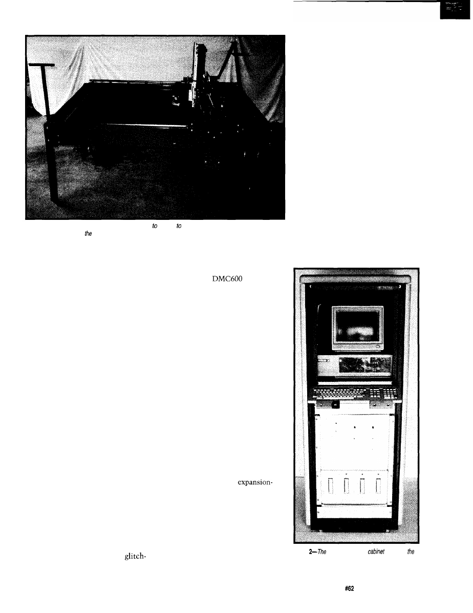
Photo l--Work proceeded from mechanical construction painting final assembly. The x-axis motor cannot be
seen here since if is under work fable.
motor shaft, its moment of inertia
adds directly to the armature. Based on
this rationale, I selected a 0.75” NC
lead screw
(10
threads per inch).
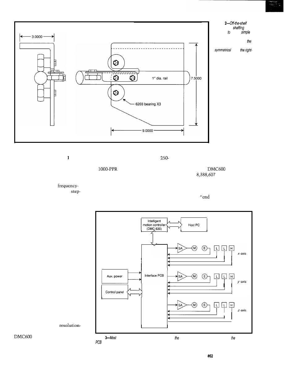
Figure 2 illustrates how I designed
the motion stages. Although this
design requires some machining, it’s
simple and repetitive since the stub
shafts are identical for x and y motion
stages.
I also needed a simple method of
holding a work piece in position on the
work surface. Commercial machines
use techniques (e.g., a vacuum) too
difficult to fabricate or too expensive. I
used a simple grid of holes containing
T nuts in a replaceable work surface. A
wooden clamp fastened by a bolt into
the T nut restrains the work piece and
keeps metal away from the cutting
area. To provide more versatility, the
table adjusts up and down with jacking
bolts.
Since the machine may have to be
moved at some time, I wanted the
mechanical design to be portable. This
machine is made with subassemblies;
each fits through a standard door
opening and most can be carried by
one person.
I spent considerable time produc-
ing detailed drawings for all parts and
assemblies. This was time well spent!
Machine fabrication proceeded
free. Photo
1
shows the results.
THE ELECTRONICS
Since at work I had become
familiar with the features and instruc-
tion of the Galil
intelligent
motion controller series, it made sense
to use it in this project. A variety of
companies make intelligent motion
controllers, so prices and features are
competitive. Some controllers install
in a PC expansion slot and some are
standalone, communicating with a PC
over a serial link.
An intelligent motion controller
solves the hardest part of system
design. Design focus shifts from
worrying about getting the system to
work to getting the system stable. The
intelligent motion controller provides
adjustment coefficients in the control
algorithm to stabilize a wide range of
mechanical systems.
The electronic portion of an
intelligent motion control system
demanded that I make choices be-
tween stepper motors and servo
motors, stand-alone and
slot, and so on.
Traditionally, stepper motors
interface with a computer for applica-
tions requiring computer position
control. However, at the time, I
couldn’t find an intelligent motion-
control card for a stepper motor which
provided coordinated motion (i.e., the
x- and y-axis speeds are altered so that
a move from one point to another is
executed via a straight line between
the two points).
In contrast, all intelligent motion-
control cards for DC servos provided
this feature. Since my application
involved cutting with a router and not
just simple positioning, coordinated
motion was essential. (In a design
incorporating new components, you
also need to choose between brushless
and brush DC servos.)
The choice to use stand-alone or
an expansion slot was easy. Stand-
alone models are intended for applica-
tions where one computer controls
several motion-control tasks, commu-
nicating serially with each controller.
Expansion-slot models tie a PC to a
single activity since the intelligent
motion controller gets its power from
the PC. For this reason, expansion-slot
models are cheaper. Since my applica-
tion needed only a single motion-
Photo
original tape-drive
becomes
xyz fable control center. The PC keyboard is on a fray
which s/ides info fhe cabinet when if’s not in use.
Circuit Cellar INK
Issue
September 1995
25
End view
Side view
Figure
bearings and
combine make a
motion stage. On/y one ha/f
of fhe stage is shown in
side view since if is
about
hand side.
measurements on the system deter-
mined the mass in motion. then
constructed transfer functions for parts
of the system. These individual
transfer functions are submitted to the
modeling package, which can then do
simulated “loop gain”
response plots and simulated
response plots.
position units are referred to as
quadrature counts. This means a
PPR encoder behaves as though it were
a
encoder!
In choosing encode resolution, you
also need to consider the total number
of pulses produced when the machine
moves from end to end. The number of
pulses is determined by the lead-screw
resolution. The intelligent motion
controller establishes the maximum
value of encoder pulses before rollover
occurs. (For the
series, the
number is
quadrature
counts.)
Limit switches are activated when
a motion stage gets close to reaching a
mechanical
of travel” limit. This
The modeled data, however,
pitch, travel length, and encoder
feature is essential if the motors have
conflicted with measured data. The
model predicted trends correctly but
could not obtain quantitative results.
While discrepancies could stem from
many factors and certainly don’t mean
the system can’t be modeled, it does
show is that even with analysis tools,
constructing a model which accurately
mimics a real system is difficult.
So, don’t choose an encoder
resolution that exceeds your require-
ments. Instead, choose the lowest
resolution that meets your needs.
Anticipate stability problems. Hope-
fully, your controller’s algorithm offers
some fine-tuning to stabilize the
system. But, to make your system
stable, be prepared to build a compen-
sator, change to a lower-resolution
encoder, or both.
SA: Servo Amplifier
M: Motor
I
Many intelligent motion control-
E: Encoder
lers employ an encoder
L: Limit switch
H: Home switch
multiplication technique. In the
series, encoder resolution is
Figure
intelligent motion control systems require elements shown here. As you can see, interface
multiplied
by a factor of four and the
plays a
central
role as a collector and distributor of signals.
Circuit Cellar INK
Issue
September 1995
27
MOTOR
X SERVO
Y SERUO
SERUO
MOTORS
SW8
SW9
X LIMIT
sufficient torque to do mechanical
damage. Most controllers have a
provision for acting on limit switch
signals.
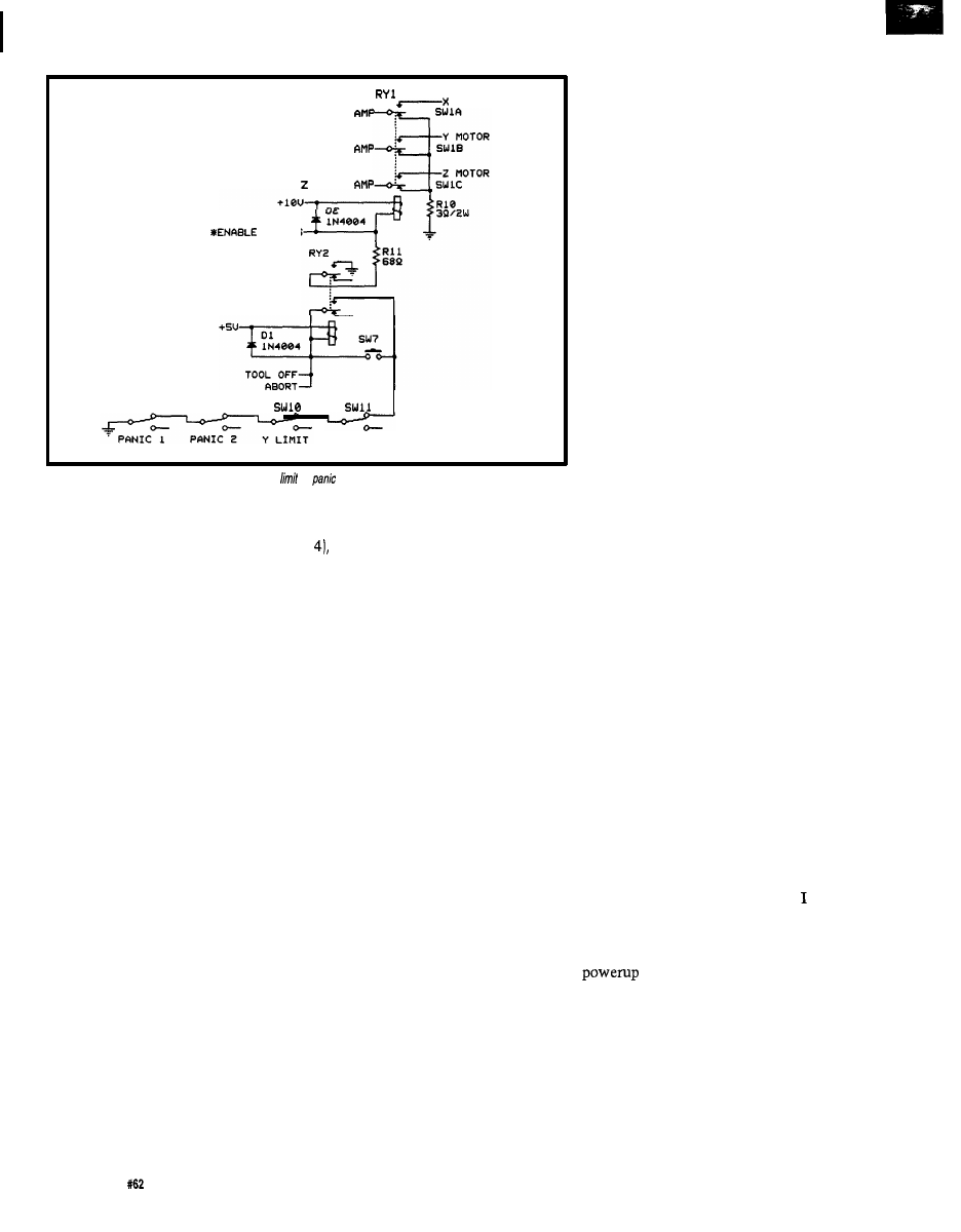
Figure 4 shows emergency shut-
down and panic switches. It’s essential
that the machine can be shut down
quickly in the event that something
unexpected begins to happen. Rather
than have users type a Stop or Halt
command, they can stop the machine
by pressing a large red panic switch
located near the machine operating
position.
Most controllers have logic-level
inputs dedicated to an emergency stop
function, but I chose to have the panic
switch deenergize a relay whose
contacts break the connection between
the servo amps and the motor. A relay
in the tape-drive power supply filled
this purpose. You can see in Figure 4
that the limit switches and the panic
switch are in a series. When any
switch opens, the motor drive is lost.
The interface PCB is a circuit
board whose main function is to
distribute signals from the controller
and gather signals for the controller. In
my system, it does some simple logic
and relay driving as well. RY2 in
Figures 4 and 5 is configured to latch
when the start switch is pressed as
long as
all
the limit and stop switches
are closed.
Figure
4-Safety features are important. Any tripped
or
switch stops the machine immediately.
A second set of contacts on RY2
energize the coil of relay RY 1 (Figure
which connects the x and y servo
amp outputs to their respective
motors. As long as RY2 stays latched,
the output of Ula (Figure 5) stays high
and the abort input is not asserted.
Abort is a software panic stop.
Ula, d, and c provide some simple
logic to turn the tool off under panic
conditions. Q2 operates a solid-state
relay (not shown), which provides AC
power to the tool. Q3 and Q4 energize
auxiliary relays, which also switch AC
power. One switches a dust collector
on and off, and the other is a spare.
The last major design problem
involved connecting cables to moving
equipment. Commercial units typi-
cally deal with this problem by using
retractile cables on small machines
and a hinged cable tray on larger
machines. I decided not to use retrac-
tile cables because I personally dislike
them and am concerned that constant
flexing might cause problems later.
The hinged cable tray arrangement
was too expensive to buy and too time
consuming to build.
Some experimenting with a rope
for a cable led to the approach shown
in Figure 6. Here, the y-axis motion
stage at one travel limit and the loop
of cable for y-axis is almost touches
the floor. When the stage is at the
other travel limit (dotted line), the
cable loop opens up and the lower part
of the loop rises from the floor. The
cable is never strained or flexed
significantly. A similar approach was
employed to install the z-axis cable.
WIRING THE SYSTEM
It is important to resist the
temptation to decrease cost and work
by hard wiring rather than installing
connectors. If an item may require
repair or maintenance, install a
connector.
The control cabinet (see Photo 2)
has sufficient cable that it can move
10 away from the XY table. This
distance keeps the PC away from the
dust as much as possible. The cabling
between the control cabinet and the
machine has connectors at each end.
There are three multiconductor cables
(one for each axis), each with a
different connector so cables can’t be
interchanged.
The bottom half of the cabinet
contains the interface PCB, servo
amps, power supply, switches, and
other electronics. Of course, these
items don’t occupy all of the available
space, but it was convenient to leave
the salvaged items mounted and wired
as they were originally. It also contains
salvaged meters which monitor the
various voltages.
COMMISSIONING
When a lot of time, effort, and
money has gone into building and
wiring a machine such as this, power-
ing it up for the first time has to
proceed carefully. I double checked
that the voltages on the wires leaving
the cabinet corresponded to the correct
voltages and pins of the encoders.
was also concerned about feedback. I
didn’t want the system to oscillate due
to instability or to run away on
because the sense of the
feedback is wrong.
Some software available from
Galil helped here. The software lets
the system power up with the feed-
back loop open (i.e., the digital control
algorithm is not yet running). This
way, you can verify that the controller
is reading the encoder correctly. The
loop is then closed. However, if the
28
Issue
September 1995
Circuit Cellar INK
system tends to run away, the loop is
immediately opened, and you are
directed to take corrective action.
Either the motor leads need to be
interchanged or the encoder channels
need to be swapped to get the sense of
feedback correct.
Once the loop can be closed
without runaway, stability problems
may still exist. The Galil software
contains an automatic tuning routine
which varies coefficients in the control
algorithm and tests the response of
your system. Continue testing until
the system response is optimal (i.e.,
fastest response with least overshoot).
The values obtained by automatic
tuning are a convenient starting point
for additional tuning with integrator
gain. Since introducing an integrator
into the loop is destabilizing, apply it
carefully. Integrator gain eliminates
steady-state positioning errors, so
I
introduced a moderate amount.
USING THE MACHINE
There is an enormous amount of
satisfaction in seeing months of
mechanical and electrical work come
together and function as intended.
Anyone familiar with assembler
programming will find this intelligent
controller straightforward. The
series has 74 instructions to
become familiar with, but you can get
started with only a handful. However,
just as assembler takes a great deal of
effort and code to perform real tasks,
so does programming an intelligent
motion controller. You soon get the
“there must be an easier way” yen.
With an additional piece of
software available from Galil, the
machine becomes part of a full-fledged
CAD/CAM system. Making programs
which direct the machine to follow a
particular path and execute a particu-
lar set of instructions becomes
virtually a drawing activity:
1. Draw the x and y path of a particular
part using any CAD system that can
produce a DXF version of the
drawing. Typical drawings include
macros to set gains and speeds,
monitor digital inputs, and activate
digital outputs. The behavior of the
cutting tool is also macro driven.
Directives indicating the tool radius
and the side of the part the cutter is
to follow are also important.
2. The DXF version of the drawing is
submitted to an application which
calculates a new path, taking into
account tool offset, and produces a
set of assembler-like motion
commands. Essentially, your
level code has been compiled into
executable assembler code.
3. Do a dry run of the DMC code on
the machine to verify that you in-
cluded everything in the drawing
that was needed for the machine to
manufacture the part correctly. It’s
important to make a permanent
record of the tool path. On my ma-
chine, the tool holder also includes a
tube which accepts a felt marker.
Like any program development
task, the steps have to be reiterated
before everything is exactly right.
Some examples of various work
samples are shown in Photo 3.
With the QED
This ready-to-use computer packs dozens of analog and digital I/O lines,
communications,
interface, and resident software on a
sized card. It delivers everything you need:
Programmable in C and Forth
l
68HC 11 microcontroller
8 and 12 bit A/D, 8 bit D/A
32 digital
lines
l
Two
serial ports
l
High current drivers
Real-time multitasking kernel
Built-in software libraries
Off-the-Shelf
Solutions Put You on the Fast Track
The QED Product Design Kit’” and Industrial Control System’” integrate the
QED Board with keypad, display and connectors in a versatile enclosure to
deliver a complete solution for your product design and control needs,
Mosaic Industries, Inc., 5437 Central Avenue, Suite 1,
Newark, CA 94560, (5
phone, (5 10) 790-0925 fax
Programming Microcontrollers in C
by Ted “an
and that is a
programming a
PC.
Van Sickle
Inside
Controlling the World with Your PC
by Paul Bergman
Use your
PC to control stepper
and
monitor fluid
switch
appliances on and off,
monitor
much more. All
directly
the parallel printer port. Complete
code
Pascal are Included on a
floppy. Each
fully
with theory,
and
disk.
fhe only book we know of where you can simultaneously learn about
fish!
reference
hundreds
show you the intimate
details of integrated circuits, hybrids,
circuit boards.
To order, call l-800-247-6553
Or
CA
Include
PO 1489,
9207
Circuit
Cellar
INK
Issue
September 1995
29
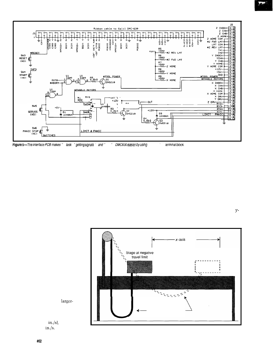
2
i
I
ENERGIZE
6
S
W
I
T
C
H
E
S
I
me
or
ro
from me
a screw-rype
DESIGN PROBLEMS AND
SOLUTIONS
Despite the best of efforts, the first
version of anything always has some
problems. Some problems here were
corrected with a minor amount of
rework, while others will have to wait
for version 2.
While using bearings as wheels for
the motion stages is functional, it does
have one minor drawback. Even
though the rails are round, they
accumulate a coating of fine dust. As
the bearing wheels pass over the dust,
it compresses and sticks to the wheel.
After 6 hours, the build-up needs to be
removed since it is not uniform and
the wheels are bumpy. Various
approaches could prevent dust buildup
on the wheels (e.g., a wiper or small air
lines). Enough time is wasted cleaning
the wheels, that stopping dust buildup
involves significant savings.
The lead screws are subject to
whipping, which means they are a
combination of too long and too thin.
Given that this system was somewhat
difficult to make stable, a
diameter lead screw would have
exacerbated the problem. Lead-screw
whip is not a problem at normal
cutting speeds (0.5
but is evident
at speeds above 2
The worst aspect to this problem
The better solution comes from
is that the stages must move slowly
removing the power supply and fan
even when the machine is not cutting.
from the PC enclosure and powering
By rotating the nut and keeping the
the PC from supplies in the cabinet.
lead screw fixed, this problem can be
Despite dusty conditions, however, the
eliminated.
drive’s heads have only been cleaned
It amazes me that the PC for this
once in two years of operation.
machine has given so little trouble
Although there has not been a
since the power supply’s cooling fan
significant problem, two areas of the
draws dust into the floppy drives. A
motion stage mechanical rigidity need
clear plastic apron in front of the drive
to be improved. Some flexing of the
openings slows the dust buildup in the
axis support beam can be observed
floppy drives, but has not stopped it.
when the tool is lowered into a work
travel
Stage at positive
travel limit
Cable to y-and z-axes
Figure 6-By elevating one end of the cable, the stage can move without stressing or damaging the cable.
30
Issue
September 1995
Circuit Cellar INK
Photo 3-A wide
range of
can be made machine such as letters of various sizes and
materials, key
racks, and holders for
CDs
and floppy disks.
piece. The y-axis support beam also
The racking of the y-axis support
racks somewhat in the x and y plane if
beam in the x and y plane could be
a x-axis retarding force is applied on
eliminated by a double-lead screw
one end and not the other due to
drive. Instead of one lead screw in the
flexing of the bearing mounting plates
middle, there should be one close to
on each end of the y-axis support
each end, thereby eliminating racking
beam.
completely.
q
Gordon Dick is a Eng. who
teaches
electronics at Northern Alberta
Institute of Technology in Edmonton,
Alberta. He also operates a small
business selling the services of a
computer-controlled
table. He
may be reached at (403)
Galil Motion Control, Inc.
575 Maude Ct.
Sunnyvale, CA 94086
(408) 746-2300
Fax: (408) 746-2315
Servo Systems Co.
115 Main Rd.
Box 97
Montiville, NJ 07045-0097
(201) 335-1007
Fax: (201) 335-1661
407
Very Useful
408 Moderately Useful
409 Not Useful
$129.95 FOR A FULL FEATURED SINGLE
30ARD COMPUTER FROM THE COMPANY
BEEN
SBC’S SINCE
5. THIS BOARD
READY
TH
30535 PROCE
I S
CODE
A KEYPAD
A N L C D
AND YOU HAVE
STAND ALONE CONTROLLER WITH
AND DIGITAL I/O. OTHER FEATURES INCLUDE:
UP TO 24 PROGRAMMABLE DIGITAL I/O LINES
l
8 CHANNELS OF FAST 10 BIT A/D
l
OPTIONAL 4 CHANNEL, 8 BIT D/A
UP TO 4.16 BIT TIMER/COUNTERS WITH PWM
UP
3
SERIAL PORTS
BACKLIT CAPABLE LCD INTERFACE
l
16 KEY KEYPAD INTERFACE
l
192K OF MEMORY SPACE,
INCLUDED
ASSEMBLER MONITOR INCL.,
OPT..
P.O. BOX
2642.
CARBONDALE. IL 62902
Flat Panels Served Here
House
Specialty Monochrome LCD Kit $249
[Controllers for PC ISA Bus]
Eorth LCD/M Monochrome LCD Controller
$149
Color LCD Controller
$299
LCD, ISA Controller,
Cable Bocklite Inverter)
Monochrome 9.4” Kit
$249
Color Single Scan 8.2”
$450
Dual Scan 9.4”
$749
Color 9.4 TFT
$995
Only)
Mono 9.4” LCD
$95
Color 9.4” Single Scan
$125
Color 9.4 Dual Scan
$399
Solutions
F!O. Box 7089 Laguna
California 92607
Phone: (714) 448-9368 Fax: (714) 448-9316 BBS: (714) 448-8093
Circuit Cellar INK
Issue September 1995
31
DEPARTMENTS
Firmware Furnace
From the Bench
Silicon Update
Embedded Techniques
Ed Nisley
Journey to the Protected Land:
Entering Virtual-86 Mode
Looking at the design of the ‘386 without a
historical perspective, it would be hard to
imagine what possible use there is for a special
mode whose purpose is to restrict the function-
ality of the processor and introduce obviously
inefficient execution. You might ask: “Why
would anyone run anything in this silly mode!”
Microprocessors: A Programmer’s View
by Dewar and Smosna
the entire Intel
mode” run rampant.
Even ignoring market-share envy, their
accusation has a grain of truth. The
‘386 architecture is gruesomely
complex in comparison to early RISC
designs. It’s less so when compared to
more recent RISC mutants, however,
which should give pause for thought.
The ‘386 CPU’s Virtual-86 mode
is a silicon-assisted PC Compatibility
Barnacle, not just a CISC feature. You
write an 8086 CPU emulator in
pure software, but acceptable perfor-
mance requires hardware assistance.
The key to V86 mode is the realization
that most instructions run on genuine
hardware with no emulation overhead
at all. Only a few operations require
custom intervention.
Why emulate an 8086 at all?
Well, because any successful PC
operating system must run
32
Issue
September 1995
Circuit Cellar INK
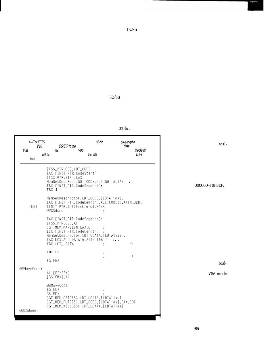
DOS programs dating back to the
Original PC. Full DOS compatibility
requires a vast infrastructure of code
emulating all the quirks built up over
the years. Perhaps someone will write
a book detailing the evolution of DOS
boxes from the advent of the 80286 to
the present-a memorial for The
Operating System That Just Will Not
Die.
The FFTS, in contrast, has a much
simpler objective. The real-mode
embedded programs I’ve covered in
previous columns can operate without
DOS or BIOS services. Although I plan
to add BIOS support, so the V86 task
won’t be completely alone down there
in the first megabyte, building a fully
functional DOS box isn’t in the plan.
Nevertheless, a great expanse of
interesting and unexplored territory
just opened up ahead of us. This
month, I’ll define the terms, set up a
simple V86 task, and show why we
need more than just
code to
make it work.
DOES VIRTUAL
q
REAL?
The ‘386 CPU emerges from a
hardware reset in real mode. The PC
BIOS gets control at the standard reset
address, goes through the usual BIOS
hocus pocus, and eventually loads a
program from diskette. When that
program is our special boot sector
loader, it pulls off a series of stunts
that culminates with the FFTS
running in
protected mode.
The Intel manuals define the
precise series of steps required for a
graceful transition from protected
mode back to real mode, none of
which apply to Virtual-86 mode. The
CPU must be in
protected mode
Listing
task
initialization routine
creates
a
code descriptor
task’s
code
segment. For
tasks, if sets
proper
real-mode address, creates a
segment descriptor
at
address, and copies code. Because
tasks do not use descriptors, if rep/aces
code
segment
descriptor
data descriptor, thus
giving monitor read-wife access task’s
code. The
initialized data segment receives similar treatment
MOV
MOV
MOV
CALL
our code seg
MOVZX
SHL
ADD
CALL
JZ
MOVZX
MOV
CallSys
MOV
CALL
MOV
MOV
MOV
MOV
MOV
XOR
MOV
MOV
INC
LOOP
MOV
MOV
CallSys
CallSys
CallSys
cvt task seg to linear
EAX,EBX
code seg + task seg
\
TaskV86
if not V86 task, done!
V86 needs numeric CS
linear seg start addr
size of code segment
\
treat as data
aim GS:EBX target
GS,EBX
save ES around loop
EBX,LDT_CODE
aim ES:EBX source
EBX,EBX
EBX
restore ES
make GS safe
before starting a task in V86 mode and,
as we’ll see shortly, it switches back to
32-bit PM after exiting V86 mode.
Thus, contrary to popular opinion,
Virtual-86 mode is not real mode.
Bit 17 of the EFLAGS register
controls what’s formally known as
Virtual Machine (VM) mode. Because
the “virtual machine” was designed to
execute real-mode 8086 programs,
Virtual Machine mode is commonly
called Virtual-86 mode. Just to keep
things confusing, that EFLAGS bit is
called VM rather than V86.
In normal 32-bit PM operation,
the VM bit is zero and the CPU
behaves as we’ve come to expect.
When a 32-bit PM task sets VM,
however, a new set of rules applies.
First and foremost, V86 mode
renders everything we’ve learned about
protected-mode segment registers,
descriptors, and selectors completely
inoperative. The CPU suddenly
generates addresses in classic
mode style: shift the appropriate
segment register’s contents left by four
bits, add a 16-bit offset, and send the
resulting value out as a memory
address.
In both real and V86 modes, the
CPU can address 1 MB plus 64 KB
minus 16 bytes:
the
result of adding FFFFO and OFFFF. The
original AT includes a gate on address
line A20 to restrict addresses to
OOOOO-FFFFF, but that gate must
remain on in protected mode. As a
result, rude V86 tasks can scribble on
the first 64 KB (minus 16 bytes) of
RAM beyond the 1 -MB line.
Of more importance, V86 tasks
cannot address memory beyond that
limit. We must copy the V86 task’s
instructions and data to RAM below
the l-MB line before entering V86
mode. The segment registers must
point at those addresses with
mode contents, not segment selectors.
Unlike 32-bit PM code,
programs do not use GDT or LDT
descriptors.
The ‘386 CPU’s memory-paging
hardware can relocate V86 tasks
anywhere in memory and prevent
them from writing into that 64-KB
block above 1 MB. Activating that
machinery is sufficiently complex that
Circuit Cellar INK
Issue
September 1995
33
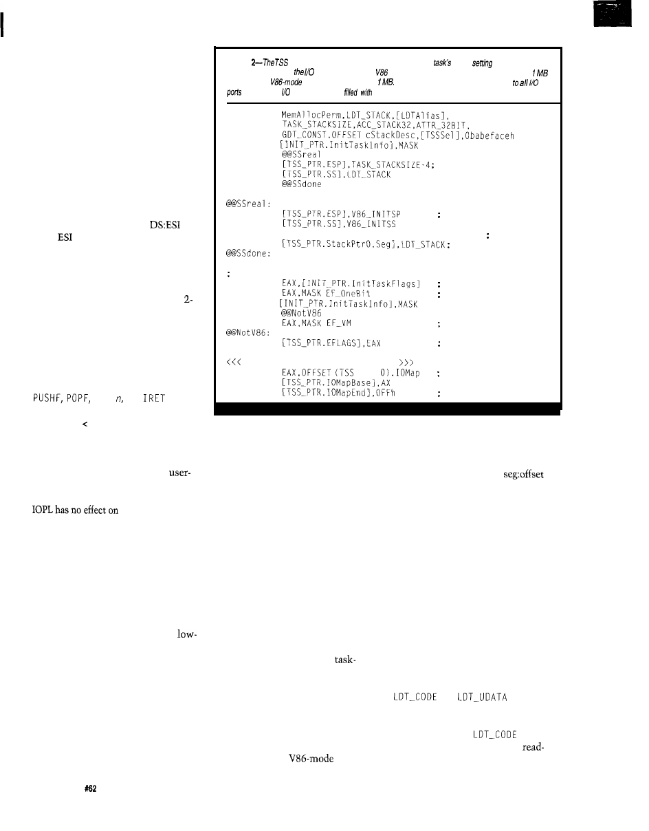
I’ll stay with a single, well-behaved
V86 task for quite a while.
V86 mode also affects how the
CPU executes some instructions. Once
again, contrary to popular opinion, the
CPU is not restricted to just 8086
instructions. Nearly all real-mode
instructions are available and you may
perform 32-bit operations if you apply
an operand-size prefix byte to each
instruction. The FS and GS segment
registers come in handy, too!
Address offsets must remain
within real-mode limits, however. If
you address memory using
when
exceeds FFFF, for example,
the CPU generates a protection
exception. When you need more than
64 KB in a segment, V86 mode is not
the right hammer for the job!
In
INK 57, I described how the
bit IOPL field in EFLAGS restricts
access to various instructions. V86
tasks, by definition, run at privilege
level 3 (also known as Ring 3) and, like
all other user-level tasks, should not
have unrestricted access to sensitive
system facilities. The C
L I, ST I,
INT and
in-
structions cause a protection exception
when IOPL 3. You can set IOPL = 3,
bypass the protection hardware, and
jam the system if you like.
In 32-bit protected mode, the IOPL
field also determines whether a
level task can execute I/O instruc-
tions. In V86 mode, oddly enough,
IN, INS,OUT,
and
OUTS.
Instead, the CPU checks the
I/O Permission Bitmap in the task’s
TSS during each I/O instruction. If the
bit corresponding to the I/O port’s
address is set, the CPU generates a
protection exception.
Some instructions, such as
LGDT,
L I DT,
and
L I DT,
are completely off
limits in V86 mode because you can’t
twiddle key CPU registers from a
privilege task. You may not stop the
CPU with a
H LT
instruction, either!
These instructions cause a protection
exception if the CPU encounters them,
regardless of the current IOPL setting.
The Intel manuals describe which
instructions are valid in V86 mode
(most are) and what happens when you
use the others (a protection exception
of one kind or another). For the most
Listing
initialization code finishes its job by creating the
stack,
up a variety of
registers, and loading Permission Bitmap.
tasks require two stacks: one in memory below
for use by the
code and another above
For simplicity, this code grants access
by leaving the Permission Bitmap
zeros.
CALL
\
\
TEST
TaskV86
JNZ
MOV
set PM task stack
MOV
JMP
MOV
set V86 stack
MOV
MOV
[TSS_PTR.StackPtrO.Offl,TASK_STACKSIZE-4 Ring-0
MOV
PM stack
set EFLAGS register in the TSS
MOV
EFLAGS register
OR
force this bit ON
TEST
TaskV86
JZ
OR
set VM if appropriate
MOV
ram it into the TSS
general register setup omitted
MOV
PTR
bitmap offset addr
MOV
MOV
set reserved byte
part, user program code isn’t bothered
by the V86 restrictions. Embedded
system and operating system code is a
little harder to write. We’ll tailor V86
mode and make things work out right
in upcoming columns.
In short, while V86 mode isn’t
really
real mode, it’s close enough for
us.
CRACKING THE GATE
Just like all other tasks in a ‘386
system, each V86 task is defined by a
TSS. The cleanest way to enter V86
mode is an ordinary task switch,
which means the TSS fields define the
state of the CPU’s registers at the start
of the V86 task. A slightly tweaked
version of the familiar FFTS
creation code is enough to set up a V86
task.
Each FFTS task has a small
structure defining its code and data
segments, shown in
INK 55, Listing 2.
In the last few columns, I’ve quietly
added a few bits and, this month, a
new bit identifies
tasks.
Perforce, that bit is zero for 32-bit PM
tasks.
The V86 task’s segments must be
below
1
MB so real-mode
addresses can reach them. Because
we’re using real-mode tools to generate
the FFTS code, Locate has already
assigned an address to the task’s code
and data segments. All we must do is
copy them from the FFTS disk image
to the appropriate address. Listing
1
shows how it’s done.
A protected-mode program cannot
access storage without a read-write
data descriptor, even when the
addresses are below 1 MB. The
initialization routine creates a tempo-
rary data descriptor covering the target
code segment before copying the data.
The offsets in both segments are
identical, with ES and GS holding the
and
sourceand
target selectors, respectively.
The routine then copies the data
descriptor into the
descrip-
tor, giving the 32-bit PM code
write access to the V86 code segment.
34
issue
September 1995
Circuit Cellar INK
I’ll show why this is vital later on. For
now, remember that we’ll never
execute the code in
PM and,
thus, don’t need a code descriptor for
it. If you’re particularly fussy, you can
choose another name for the LDT
segment. By the way, this is probably
the most roundabout way imaginable
to get real-mode code into its proper
location.
Snap quiz: how many copies of the
V86 code and data segments are in
storage after the task initialization
code gets done with them? Extra
credit: how does the FFTS code know
where to put the segments!
The initialized data segment in
receives
similar treatment.
The
task this month doesn’t
use any data, although there is a single
placeholder variable. Check the source
code on the BBS for all the grim
details.
Listing 2 shows the stack setup
routine. The V86 code must have
mode addresses in SS:SP, which I load
with
for historical reasons.
That’s just below the default disk
Listing
3-This Virtual-86 task writes
info
the video buffer using ordinary real-mode addresses. The
In 20 instruction causes a protection exception that invokes the V86 monitor.
includes USE16 seg size
MOV
find CRT controller address
MOV
ES,AX
MOV
MOV
assume color
CMP
is it so?
JE
MOV
n o p e , reset to monochrome
MOV
ES,BX
aim
at video buffer
MOV
the very last character!
MOV
[BYTE PTR
make it white on black
XOR
set up char counter
MOV
set up for scope blips
@Again:
IN
set trace blip
OR
OUT
MOV
INC CX
PUSH CX
MOV
pop char into video buffer
and step to the next one
exercise the stack
(continued)
Energy Management
A
Access Control
A
Coordinated Home Theater
Coordinated Lighting
Monitoring Data Collection
Get all these capabilities and more
with the Circuit Cellar
Park Street, Vernon, CT 06066
Assembled $65
1
Kit
$461
GET STARTED TODAY WITH AN HCS2
The
consists of an
board, Relay BUF-Term board,
PL-Link board,
power-line interface, PS
1 power supply,
serial cable, and
HCS
software.
36
Issue
September 1995
Circuit Cellar INK
Listing
3-continued
@Stall:
LOOP @@Stall
add a non-trivial delay
IN
AND
AL,NOT
OUT
INT
20h
POP cx
JMP @Again
ENDP
clear trace blip
crash into V86 monitor...
restore CX after switch!
repeat forever
bootstrap load point, a magic number
that will come in handy later on.
The initialization code also loads a
TSS field that we haven’t used before:
the Ring-O SS:ESP registers. When an
interrupt occurs in a Ring-3 task, the
CPU must find a Ring-O interrupt or
trap gate in the IDT. It switches from
the user task’s Ring-3 stack to the
Ring-O stack defined in the TSS before
pushing any values. Our new V86 code
is the first task we’ve seen that doesn’t
run at privilege level O!
The remainder of Listing 3 sets up
EFLAGS and the I/O Permission
Bitmap. The code turns on the VM bit
in EFLAGS and leaves IOPL set to
zero. This operation ensures that the
restricted instructions described above
will cause a protection exception; the
V86 task cannot do something rash
like disable all hardware interrupts or
clobber the EFLAGS register.
I included the I/O Permission
Bitmap in the intial TSS definition a
few months ago, but did not activate
it. V86
must have a valid bitmap
because the CPU refers to it when
executing I/O instructions. The Intel
explains why the byte just after
the table must be filled with
this
was actually a workaround for a bug in
early ‘386SX chips.
Each bit in the I/O Permission
Bitmap controls access to a single
byte I/O address. If the bit is zero, I/O
operations in user-privilege tasks may
use that port. If it’s one, those tasks
cause a protection exception. A
(2-byte) port has two associated bits
and a 32-bit (4-byte) port has four. It’s
that simple!
For the moment, the bitmap is
even simpler because it grants unre-
stricted access to all I/O ports. Recall
that the setup code clears all of storage
above
1
MB, including the locations
that hold the TSS.
The FFTS task initialization code
produces the trace output shown in
Figure 1. Pay particular attention to
EFLAGS and the segment registers.
The LDT contains three data descrip-
tors covering the task’s code,
8051 C251
EMBEDDED CONTROLLERS
Corporation introduces its newest board, the
designed for Intel’s
chip.
RIGEL builds and
supports 8 and
bit development tools for embedded controller systems. We
eature hardware, software, books, and kits, for educational and
ndustrlal markets.
RIGEL DIFFERENCE
of our boards come
with:
32K RAM or EEPROM
Machine screw sockets
l
Power on LED
l
All system signals
on headers
l
available on
terminal blocks
l
Sample programs
l
Circuit diagrams
l
Assembly language
IDS software READS
l
support
Our entire line
of
8051 boards are
programmable in
Assembly, BASIC,
and Forth. We also offer a low cost Fuzzy
Logic Software code generator and a chip simulator for the 8051
family.
Complete systems start at $85
CALL TODAY FOR MORE INFORMATION
RIGEL Corporation,
PO BOX 90040, GAINESVILLE, FL 32607
Telephone (904) 373-4629 BBS (904) 377-4435
*Simple
external power required
Analog inputs (12 bit)
3 Digital I/O lines
with the included software or
with your own DOS or Windows
(Windows DLL provided)
to Excel or other
applications
software available
Route 72 West Suite C-178 Manahawkin, NJ 08050-2890
FAX-BACK INFO : (609)
BBS
: (908) 774-7499
TO
ORDER : (800) 341
n
5590
OUTSIDE US:
872-8355
Circuit Cellar INK
Issue
September 1995
3 7
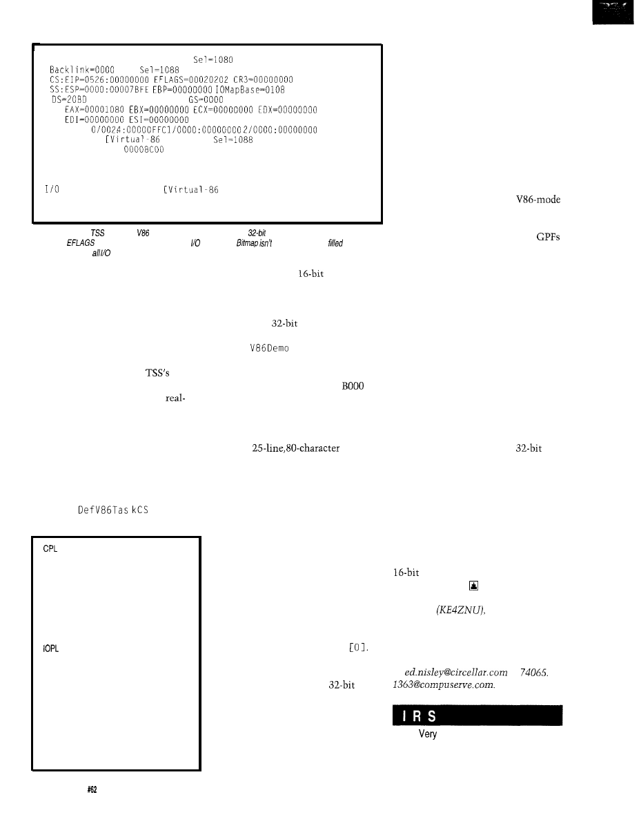
TSS Dump of [Virtual-86 Demo1
Base=00131000
LDT
Trap=0000
ES=0000 FS=OOOO
S S : E S P
L D T D u m p o f
Demo] LDT
0004: 003034DE
oooc: 52600039 00009300
0014: OBD00003 00009302
0024: 3ACOOFFF 0040926A
P e r m i s s i o n B i t m a p o f
D e m o ]
p o r t +
00
20
4 0
60
( a l l p o r t s e n a b l e d )
Figure l--The initial
fields of a
task distinguish it from ordinary
PM tasks. In particular, note the
contents of
and the segment registers. The Permission
listed because it’s
with zeros
that allow access to ports.
ized data, and stack segments. There is
no uninitialized data segment.
The FFTS task dispatcher starts
the V86 task by executing a
FAR J M P
to an address containing the task’s TSS
selector. The CPU stores the current
task state in the old TSS and loads the
V86 task’s state from the new TSS.
Because the VM bit in the
EFLAGS field is set, the CPU inter-
prets the contents of CS:EIP as
mode address bits and begins execut-
ing the first instruction in the task.
For all intents and purposes, we’re
back in real mode.
BEYOND THE FENCE
Listing 3 shows the simple V86
task we’ll use for the next two col-
umns. The
macro
includes a USE 16 segment size
Current Privilege Level
DPL
Descriptor Privilege Level
EOI
End Of Interrupt (command)
FDB
Firmware Development Board
FFTS
Firmware Furnace Task Switcher
GDT
Global Descriptor Table
GDTR
GDT Register
IBF
Input Buffer Full
IDT
Interrupt Descriptor Table
IF
Interrupt Flag
I/O Privilege Level
LDT
Local Descriptor Table
LDTR
LDT Register
NT
Nested Task
OBF
Output Buffer Full
P bit
Present bit (in a PM descriptor)
RF
Resume Flag
RPL
Requestor Privilege Level
TF
Trap Flag
TR
Task Register
TSS
Task State Segment
VM
Virtual Machine (in EFLAGS)
specifier that forces
data and
addresses. If you use a 32-bit register or
data value, the assembler inserts an
operand-size prefix byte that switches
the CPU into
mode for that
single instruction.
The
code determines the
video buffer address and creates a
pointer to the bottom-right character.
The segment address is either
or
B800, just as in real mode, and these
values do not refer to magically
created GDT or LDT selectors. I hard
coded the character offset for an
ordinary
screen
rather than fiddle with all the BIOS
values. Feel free to tweak the code for
your system.
The task’s endless loop wiggles a
parallel port bit using ordinary I/O
instructions, then increments CX [not
ECX!) and writes CH into the video
buffer. You get easily visible indica-
tions that the task is executing, the
code can access the video buffer, and
the stack works correctly.
Although the loop may be endless,
there must be a way to return control
back to the FFTS task dispatcher. In
32-bit PM tasks, we use a FAR JMP to
the dispatcher’s call gate in
LDT
In
V86 mode, that won’t work because
we don’t have access to the LDT. In
fact, we can’t even create a
gate
address, let alone call it!
The CPU exits V86 mode when a
hardware interrupt or protection
exception occurs. V86 tasks must be
carried through the door feet first on a
stretcher; there’s no graceful way out.
The I NT 20 instruction near the
bottom of the loop in Listing 3 triggers
a protection exception because IOPL =
0. The CPU invokes the infamous
General Protection Fault handler at
I n t 0 D. The PM error handler
displays the address of the failing
instruction, dumps the TSS values,
and halts the system.
Feet first and face down!
Obviously, that’s not the proper
response to a software interrupt in-
struction. If you plan to run
tasks in your system, you must pro-
vide what’s called a “V86 monitor”
routine. That monitor intercepts
and other error conditions, examines
the situation, and does whatever is
required to keep the V86 task running.
In this case, the monitor should pass
control to the FFTS task dispatcher,
which starts the next task in its list.
I must postpone describing the
monitor until next month. Rest
assured, however, that the code on the
BBS has both the V86 task and a
simple monitor to keep it going.
Download the files and you’ll have a
headstart on next month’s discussion.
RELEASE NOTES
This month, we add a single Vir-
tual-86 taskette to the three
protected-mode taskettes. The 16-bit
code blips a parallel port bit and writes
directly into the video buffer, which is
enough to demonstrate it works. Most
important, the CPU can address mem-
ory with real-mode segments in what’s
otherwise a protected-mode program.
Next month, we’ll build a simple
V86 monitor routine that tosses the
task back through the door head
first and kicking.
Ed Nisley
as Nisley Micro
Engineering, makes small computers
do amazing things. He’s also a
member of Circuit Cellar INK’s
engineering staff. You may reach him
at
or
410
Useful
411 Moderately Useful
412 Not Useful
38
Issue September1995
Circuit Cellar INK
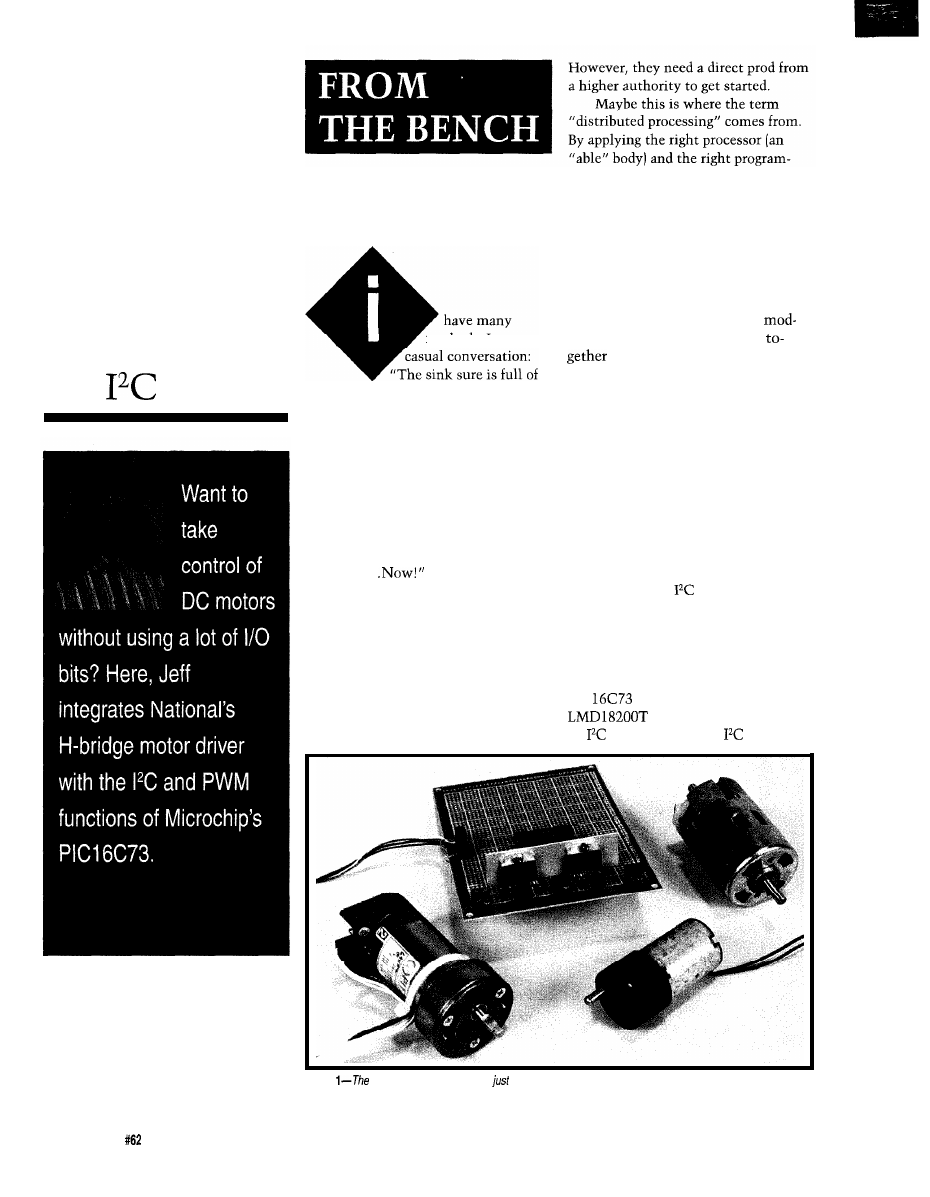
Creating the
Smart-MD
DC Motor
Control for
the
Bus
ming (don’t mow over Mom’s flowers),
Jeff Bachiochi
you can simplify a major task to single
command. This leaves the main pro-
cessor (namely, me) to go on with the
other tasks at hand (wash the car, pay
the taxes, or finish writing this article).
THE SMART MODULE
I see a growing demand for
methods. I can use
ules which can be easily pieced
to form a single system. Each
module contains the smarts to perform
dishes,” which is greeted with silence.
There’s the looking-for-sympathy
method: “Does anyone know where I
can find a clean spoon.” Silence.
Then, there’s the eliminate-the-excuse
method: “Oh look, we’re really not out
of dish detergent.” Silence.
If you have children, you know
these methods rarely work. You’ve got
to get straight to the point. “Alicia, do
the dishes..
And, it’s no different with my
sons. I try to add a bit of humor, “Did
you lose the lawnmower in the grass
again?” And, it backfires, “No, Dad, I
can still see the top of the handle.”
It’s not that kids are dumb. Au
contraire, they are extremely intelli-
gent. They are entirely competent to
complete every task asked of them.
a special task.
Smart modules are strung together
with a main processor which collects,
analyzes, and directs data while per-
forming higher-level functions. When
the system components (smart mod-
ules) are local to one another as with a
robot, no special transmission drivers
are needed.
Although the communication
interface could be any number of pro-
tocols, I’m using
because it is easy
to implement on most processors with
only two I/O lines.
Photo
1
displays the first module I
want to introduce: the H-bridge motor
driver, or Smart-MD. This consists of a
PIC
processor and two
chips. The PIC looks like
an
slave device to an
master. It
Photo
Smart-MD module contains
three chips and acts as an PC slave capable of controlling twin 3-A
H-bridge motor drivers.
40
Issue
September 1995
Circuit Cellar INK
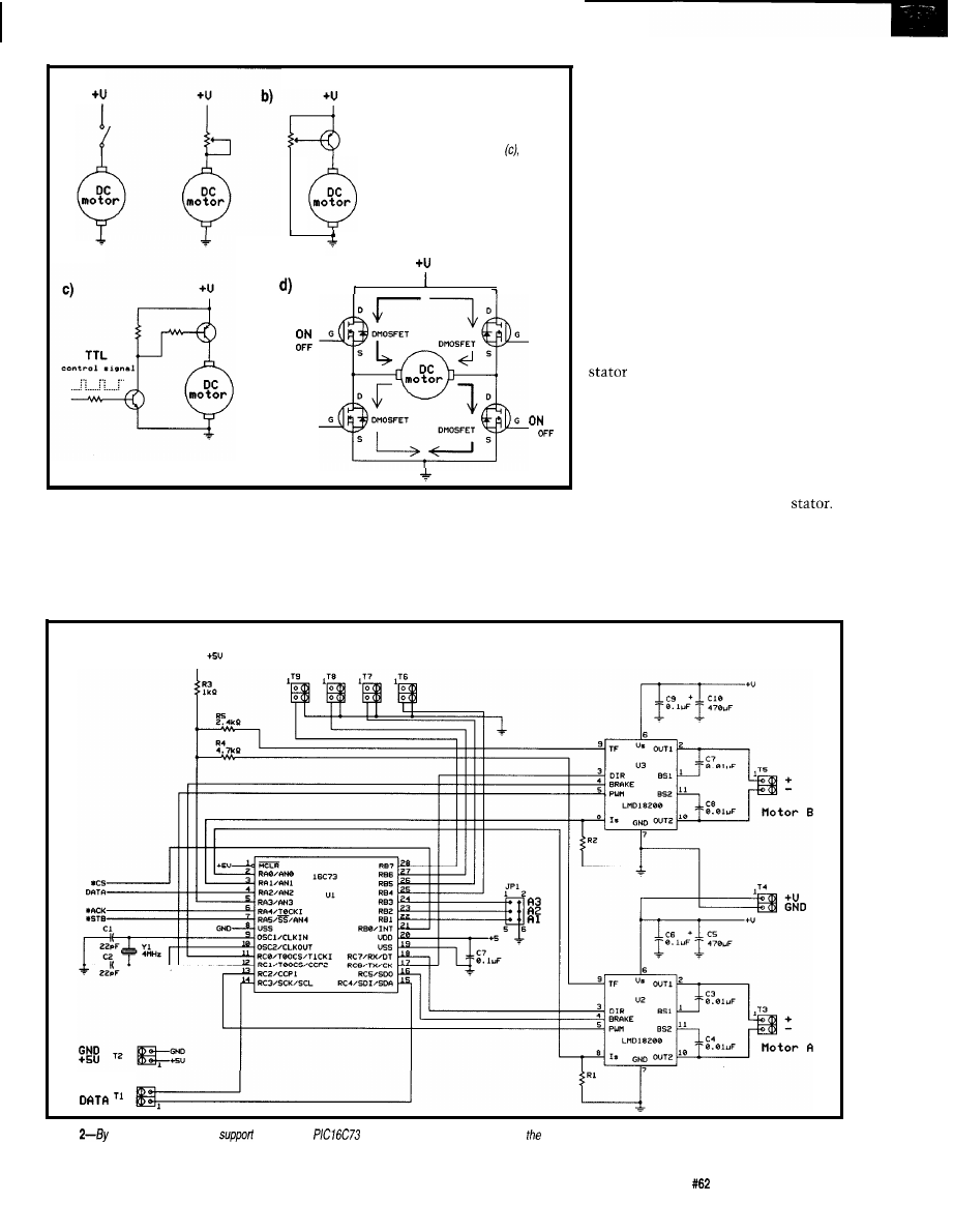
a)
applied. They require multiphase con-
Figure l--Trace the
evolution of
motor control. Starting with a simple
trol signals which energize field coils
on/off switch and variable resistor (a),
arranged sequentially around an arma-
we then go to a variable semiconduc-
ture made of permanent magnet poles.
tor drive (b), PWM control and a
As each coil is energized, it draws
full-control H-bridge which includes
direction.
the closest armature pole toward it so
the shaft steps or partially rotates and
then holds position until the next coil
is energized. The rotation speed is
based on the speed of the sequencing
field coils. The step size (degrees per
step) is determined by the number of
coils.
In contrast, PM DC motors run
OFF
full speed while a constant DC voltage
ON
is supplied. The PM poles make up the
and are located around the out-
side. The coils are wound around the
OFF
ON
armature and connect to the DC volt-
age source through opposing brushes,
which contact only one step of arma-
ture coils at a time.
When a coil is energized, it is
drawn toward a PM pole of the
performs PWM, braking, direction
PM DC MOTORS
This rotates the armature shaft in a
control, and limit switch sensing for
I’ve done projects with stepper
step similar to the stepper motor, only
two PM DC motors. Each motor driver
motors in the past, but not DC motors
now the coil becomes disconnected
can supply 3 A of continuous current
with brushes. Stepper motors don’t
from the DC source as it rotates away
at up to 55 V.
move while a constant DC voltage is
from the stationary brushes. Mean-
Limit Switches
r
2a 2b
la lb
CLK
Figure
using the PC and PWM
built into the
and some dedicated H-bridge chips, Smart-MD twin motor drive controller requires just three chips.
Circuit Cellar INK
Issue
September 1995
4 1
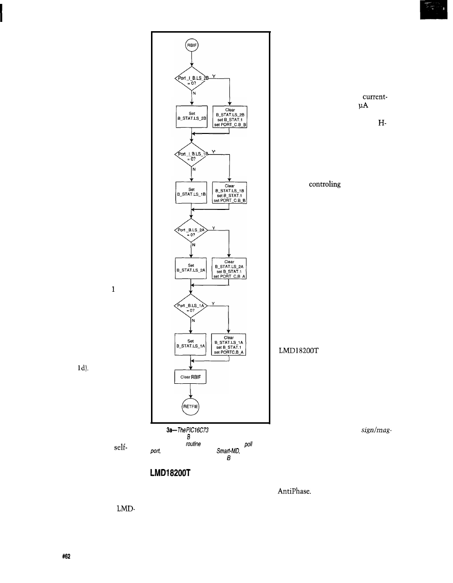
while, the next coil becomes energized
and continues rotating the shaft. This
rotation continues as long as DC volt-
age is applied. The speed is based on
the amount of DC voltage.
The simplest motor control is a
switch in series with the motor. Re-
place the switch with a pot and you
can control the motor’s speed (Figure
la). Both the switch and the pot can be
replaced by a transistor. However,
when operated in its linear region, the
transistor must be able to dissipate a
good deal of power [Figure lb). Drop-
ping half the power across the transis-
tor is a total waste-or at least half a
total waste.
The trick is to use the transistor
as a switch, not a pot, and to halve the
power using pulse width modulation
(PWM). Turn it on for half the time
and off for the remainder. By varying
the duty cycle (on time vs. off time),
you can have variable motor speed
without wasting power (Figure lc).
Better yet, the motor gets to run at its
rated voltage for ultimate performance,
Most transistors have considerable
drop even when driven into saturation.
This drop can be in excess of V,
which represents a lot of wasted heat.
DMOS switches reduce this waste to
under 0.5 V and provide faster switch-
ing times than bipolar transistors.
To reverse the rotational direction
of a PM motor, you must reverse the
DC power source. This requires four
switching devices set up in an H con-
figuration (Figure
Only two diago-
nal devices can be switched on at once.
While one set is on, current flows
through the motor in one direction.
When the opposite set is on, current
flows in the opposite direction. If de-
vices on the same side were inadvert-
ently turned on together, they would
create a short across the DC source,
resulting in high currents and
destruction.
Fortunately, no one writes code
which could cause this to happen. But,
if you’re concerned, you can prevent
this by using a device that contains the
H-bridge in one discrete package.
National Semiconductor’s
18200T is just the beast. It comes in an
11 -pin power SIP. And no, it’s not new;
just packed with features.
N
=
N
Clear
Figure
can generate an interrupt
whenever a Port input bit changes state. By using an
interrupt service
instead of having to
the
code is simplified. On the
the motor
limit switches are connected to Port inputs.
The bit can operate in two modes.
The normal mode is called
nitude. Here the direction bit directly
controls the direction, while the PWM
controls the speed or torque from full
on (100% duty cycle) down to full off
(0% duty cycle).
The H-bridge is made with DMOS
The alternate mode is the Locked
power transistors for lower drop and
In this mode, the PWM
faster switching speeds. Each switch
input bit is held at logic high while a
contains its own intrinsic protection
PWM signal is applied to the direction
diode and is made up of many parallel
input bit. A PWM input with a 50%
devices which equally share total cur-
duty cycle, although enabling the mo-
rent.
tor in opposite directions on each half
Because of this sharing, total de-
vice current can be measured by di-
recting a single cell’s output to a
current-sourcing output. This setup
gives the user a way to measure motor
current without adding a series resis-
tor to the circuit and consequently
losing precious power. The
sourcing output gives 377
for 1 A
of motor current.
Three input bits control the
bridge: direction, PWM, and brake.
The direction bit controls which di-
agonal pair of switching devices is
used and switches the appropriate
upper device on. This switching con-
trols the rotational direction of the
motor by
the direction the
current passes through the motor.
A logic high on the PWM input
enables the lower device so full cur-
rent flows through the motor. A logic
low disables the lower device and
interrupts the current flowing through
the motor.
The last input, the brake bit,
shorts out the motor by turning on
either the top or bottom two devices,
depending on the direction bit.
One disadvantage of using DMOS
over bipolar transistors is they require
their gates to be about 10 V higher
than their source voltage to fully turn
on. When you’re looking for simplic-
ity, this requirement frequently com-
plicates the circuitry. However, the
has built-in charge-pump
circuitry which creates the necessary
control voltages so the interface can be
TTL compatible.
Although the PWM input bit can
be a simple logic high to turn the mo-
tor on, applying a PWM signal gives
speed and torque control of the motor.
42
Issue
September 1995
Circuit Cellar INK
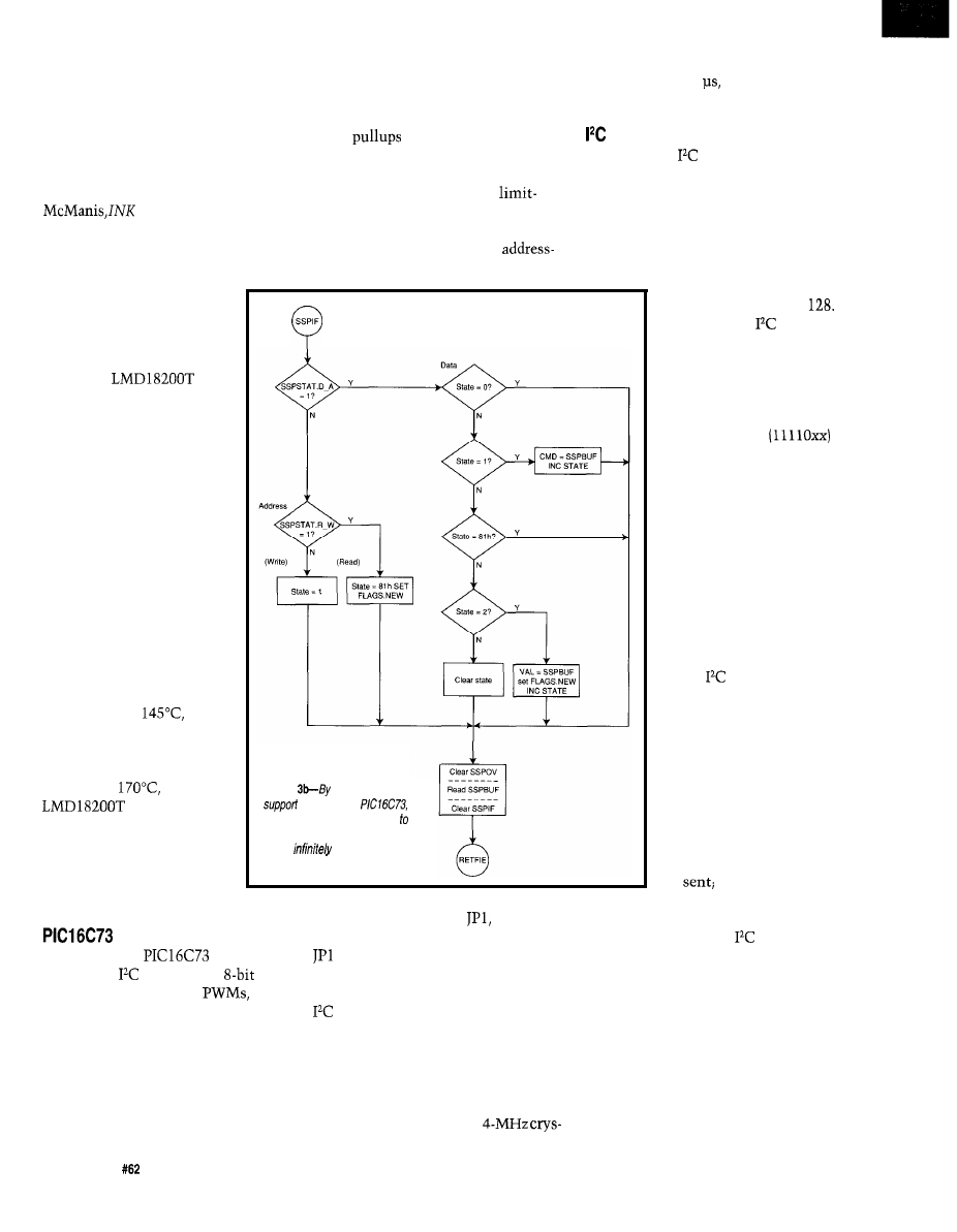
cycle, averages a current flow of zero
and thus has no movement.
Changing the duty cycle one way
or the other unbalances the average
current, which controls the motor’s
speed, torque, and direction, all from
the same single signal (see “NC-based
Motor Speed Controller” by Chuck
60).
Figure 2). I use the remaining bits of
tal for the simple reason that instruc-
Port A as digital I/O (these will be
tions execute in 1
which makes
discussed in more detail next month].
cycle counting easy.
I chose to use sign/magnitude
control because it offers the same
PWM signal with twice the resolution.
Port B can be configured with
weak
on all of the bits used as
inputs. This configuration avoids the
need for an external resistor SIP. The
upper four bits on Port B are
switch inputs and are treated as
change-of-state interrupts. The next
three lower bits of Port B are
selection inputs. Any jumpers placed
By now you’ve seen the
advantages of using a mono-
lithic drive controller, but
I
want to mention some of
the other built-in advan-
tages. The
has
overcurrent protection. It
shuts off the upper H-bridge
devices whenever (if ever)
the current reaches 10 A.
The device checks for this
fault every few microsec-
onds and clears itself if the
fault has been removed.
Since the DMOS de-
vices require the charge
pumped 10 V over the
source voltage, there’s a
low-voltage lockout which
only permits operation
when the source voltage
exceeds 10 V.
If the device reaches a
temperature of
an
output bit is pulled low to
signal the user of impending
doom. Should the tempera-
ture rise to
the
automatically
disables all four DMOS
devices, preventing catastro-
phe. A little built-in hyster-
esis reactivates the H-bridge
when the temperature falls.
Figure
using the PC
built info the
dealing with the bus is similar
working with any other serial port
and is
easier than bit
banging.
on the address selector,
ground the
device.
The basic
transmission con-
sists of an address byte and a data byte.
Within the address byte, the upper 7
bits contain the actual address while
the least-significant bit is used as a
read/write indicator. While this sim-
plifies the protocol, it also limits the
number of devices on the
bus to a maximum of
Since the
protocol
was first introduced, en-
hancements have been
made to increase the
available addresses and
throughput. A particular
set of addresses
can indicate that the byte
following contains an
additional 8 bits of address
information. I can’t imag-
ine using more than 128
devices [where have I
heard this before?), so for
now, I’m not supporting
the expanded mode.
There is a slight dif-
ference between the write
and read transmissions.
Many
peripherals are
quite dumb and require
only one byte of data. The
smarter (more compli-
cated) ones have multiple
registers for the data. This
situation requires that an
additional byte be sent
when writing (address,
register, and data bytes).
More data bytes can also
be
however, this is
predetermined by the
I chose the
because it
contains an
interface, an
A/D
converter, two hardware
and a
total of 22 I/O lines.
The I/O lines are broken down
into ports: AO-5, BO-7, and CO-7. Port
A is used as analog inputs to the A/D
converter.
I
am using three analog
inputs: two for motor-current sensing
and one for overtemperature input (see
input pins and can be read as logic 0.
lets up to eight of these Smart-MD
modules be used in one system.
When reading, the
protocol
requires the slave to respond right after
the address, leaving no room for a
transmitted register byte, which is
where transmissions differ. Immedi-
ately after an address byte (where the
LSB is a 1, indicating a read), the mas-
ter (clock source) looks for a reply, so
the last register set up by a write is
used as the selected register to read
from.
Port C has the PWM outputs, the
bus connections, motor direction,
and brake controls for each motor.
Many of Port C’s pins are multipur-
pose. However, once you define them
in your application, the possibilities
are reduced considerably. Unless a
need arises, I like to use a
4 4
Issue
September 1995
Circuit Cellar INK
The Smart-MD interprets the
register bytes as commands. Its address
is set as
where xxx is read
from the external address jumpers.
When its address is recognized and
includes a write, the Smart-MD ac-
cepts the following register and data
byte. The register byte is interpreted as
a command. Each legal command
allows some kind of action to be taken
using the data byte. Table 1 offers a
simple command set.
TWIN PWMS
The
has two complete
capture, compare, or PWM modules.
When used in PWM mode, the PR2
register is used as the base counter and
acts as a reference to control the PWM
frequency.
In standard-resolution mode, up to
8 bits can be loaded into the PR2 regis-
ter. In high-resolution mode, which
concatenates the two internal Q clock
bits, the PR2 register can create a
bit base.
Each PWM module has a timer
which is continually compared to the
PR2 register and resets when a match
occurs. This operation produces a logic
1 on the PWM output pin. Since the
PR2 register does not change, the
PWM output pin always goes high in
exactly the same number of counts
(constant period).
A
register pair (CCPRlL and
CCPRlH) creates the actual duty-cycle
timing. The user loads a number into
the CCPRlL register. Whenever the
timer resets, the value in the CCPRlL
is loaded into the CCPRlH. This ac-
tion prevents unwanted glitches from
occurring on the PWM output when a
duty cycle is altered midcount.
The CCPRlH and the timer are
also compared. However, a match on
this register pair resets the PWM out-
put to a logic 0. You can see how alter-
ing the value loaded into CCPRlL
register affects how long the PWM
output stays high. Smaller numbers
shorten the on time, while larger num-
bers lengthen it. The value placed in
the CCPRlL register automatically
reloads CCPRlH every cycle for
hands-off operation.
Whenever a write command or
p) is received, the top bit of the data
value is placed on the direction control
output bit for the associated motor
(P=motor A and p=motor B). The re-
maining 7-bit value is multiplied by 2
(shifted left once] and placed into the
appropriate motor’s PWM CCPRlL
register. This command controls both
the direction and the duty rate for one
or the other motor. A read command
passes back the data value it last re-
ceived.
BRAKING
Each
has a separate
input bit for emergency braking. This
command stops the motor even if the
direction and PWM bits call for move-
ment.
The brake write command (B orb)
enables or disables the brake bit of the
associated motor driver, depending on
the data value received. Any value
other than 0 turns on the brake for
that motor driver.
When a read braking command is
received for either motor, the status
register is returned giving more infor-
mation than just the brake status. The
upper four bits contain the current
status of the two limit switches for
each motor. These inputs are normally
high and are grounded when a switch
is tripped.
The next two bits indicate the
current temperature of each motor
driver. Each bit is cleared when the
temperature of its corresponding driver
exceeds 140°C. The final two bits
indicate the present states of the brake
output bits for each of the motors. The
same status register is sent regardless
of whether the command was B orb.
A few words on the limit switch
inputs are called for. On the PIC, a
change of state on any Port B bit set for
input can generate an interrupt. This
feature is used to our advantage by
letting any limit switch automatically
brake its associated motor driver. Even
though the brake bits are automati-
cally set, the user can remove them
through a brake-write command. Care
and logic must be used to avoid con-
tinuing past the limit switch.
CURRENT STATUS
Motor current gives the user feed-
back on the status of the motor. It not
FREE
Data Acquisition
Catalog
PC and
VME
data
acquisition catalog
from the inventors of
plug-in data acquisition.
Featuring new low-cost
A/D boards optimized
for Windows,
DSP Data Acquisition,
and the latest
Windows software.
Plus, informative
technical tips and
application notes.
Call for your free copy
l-800-648-6589
ADAC
American Data Acquisition Corporation
70 Tower Office Park, Woburn, MA 01801
phone 617-935-3200 fax 617-938-6553
Circuit Cellar INK
Issue
September 1995
45
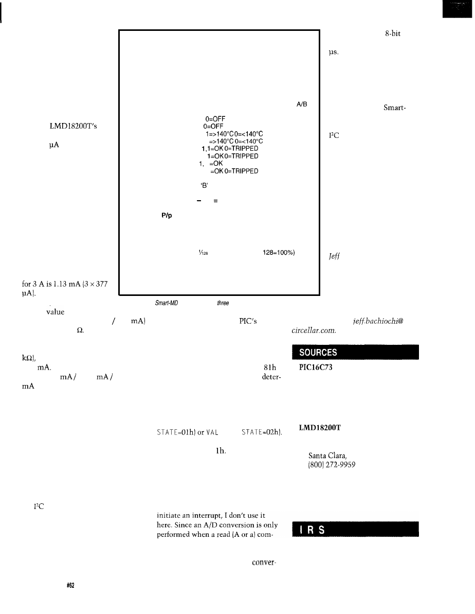
only indicates the speed of
the motor, but also how
hard it’s working. Exces-
sive current suggests a
stall, which can lead to
overheating. The user may
wish to adjust the motor’s
PWM duty cycle settings
based on these current
measurements.
The
current output pin gener-
ates 377
per amp pass-
ing through the motor. A
resistor from this pin to
ground converts the out-
put current to voltage.
You should choose a resis-
tor value which produces a
5-V drop at motor-stall
currents to prevent ex-
ceeding the A/D
converter’s 5-V maximum
input.
Let’s say the motor’s
stall current is 3 A. The
current output produced
The maximum input
Command A/a (Analog to Digital Converter)
Address
Register
Data
Action
OOOOxxxl 01000001 ‘A’ xxxxxxxx Read Current Motor A
OOOOxxxl 01100001 ‘a’ xxxxxxxx
Read Current Motor B
where data = 8-bit value of Motor current
Command B/b (Brake and status of Motor A/B)
OOOOxxxl 01000010 ‘B’ xxxxxxxx Read LS, TF, Brake A/B
OOOOxxxl 01100010 ‘b’ xxxxxxxx Read LS, TF, Brake
where data = xxxxxxxx
bit 0: Motor A brake, 1 =ON
bit 1: Motor B brake 1 =ON
bit 2: Motor A temperature,
bit 3: Motor B temperature, 1
bit 4: Motor A limit switch
bit 5: Motor A limit switch 2,
bit 6: Motor B limit switch 1
0 TRIPPED
bit 7: Motor B limit switch 2, 1
OOOOxxxO 01000010
xxxxxxxx Enable/Disable Brake A
OOOOxxxO 01100010 ‘b’
xxxxxxxx Enable/Disable Brake B
where data = 0 = OFF 1 255 ON
Command
(Direction and PWM control of Motor A/B)
OOOOxxxl 01010000 ‘P’ xxxxxxxx Read PWM of Motor A
OOOOxxxl 01110000 ‘p’ xxxxxxxx Read PWM of Motor B
where data = Oxxxxxxx is forward
1 xxxxxxx is reverse
where xxxxxxx = PWM in
increments (O=O%
ooooxxxo 01010000 ‘P’ xxxxxxxx
Set PWM of Motor A
ooooxxxo 01110000 ‘p’ xxxxxxxx
Set PWM of Motor B
where data = present PWM value
for the A/D converter is 5
Table l--The
module supports
basic commands.
V. This
is divided by
the output current (i.e., 5 V 1.13
to produce 4,424
serviced by analyzing the
SSPSTAT status bits and determining
the present state of the system. Prior
to any reception, STATE is zero.
Selecting the closest common
resistor value less than our result (4.3
the maximum current is fixed at
1.16
With 8 bits of resolution,
that’s (1.16
0.377
256) or 12
of actual motor current per bit.
PIC CODE
The flowchart in Figure 3 gives an
overview of what goes on behind the
scenes. There are basically two inter-
rupt routines. The first is the Port B
change-of-state interrupt. This inter-
rupt protects the mechanics of the
motor apparatus by shutting down
motion which oversteps the bound-
aries of the physical system.
The second interrupt routine is
the
communication. Illegal and
unnecessary interrupts are prevented
by the hardware. Only transmissions
which match the module’s address can
create an interrupt. Until a stop bit is
reached, this and any data following
causes interrupts. Each interrupt is
sion time for full
resolution is only about 14
PARTIAL CONCLUSION
Using only three de-
vices (a PIC and two
LMD 18200T H-bridge
motor drivers), a
MD module can control
two 3-A motors from an
bus. This setup is per-
fect for robot control where
the robot’s motor needs to
be stopped and started by
its sensors.
If you need accurate
positioning, catch next
month’s column. There,
decoder circuitry tracks the
motor’s position.
Until then, happy
motoring.
q
Bachiochi (pronounced
“BAH-key-AH-key”) is an
electrical engineer on Cir-
cuit Cellar INK’s engineer-
ing
staff.
His background
includes product design
and manufacturing. He
may be reached at
Once an address match occurs,
STATE is set to Olh for a write or
for a read. Since the address also
mines the read/write status, I use the
most-significant bit of STATE as an ID.
As additional interrupts occur, STATE
is incremented by 1 and the data is
temporarily stored as CMD (when
(when
Microchip Technology, Inc.
2355 W. Chandler Blvd.
Chandler, AZ 85224-6199
(602) 786-720
Fax: (602) 899-9210
National Semiconductor Corp.
P.O. Box 58090
CA 95052-8090
The main program loop looks for a
STATE of 03h or 8
When either is
found, the CMD register is used to
identify which subroutine should be
executed. When finished, the state is
Digi-Key Corp.
cleared and a jump is made back to the
P.O. Box 677
loop to await further instructions.
Thief River Falls, MN 56701
Although the A/D converter can
(800) 344-4539
mand is received, a simple poll of the
conversion bit *DONE is used for
simplicity. Total settling and
413
Very Useful
414
Moderately Useful
415 Not
Useful
46
Issue
September 1995
Circuit Cellar INK
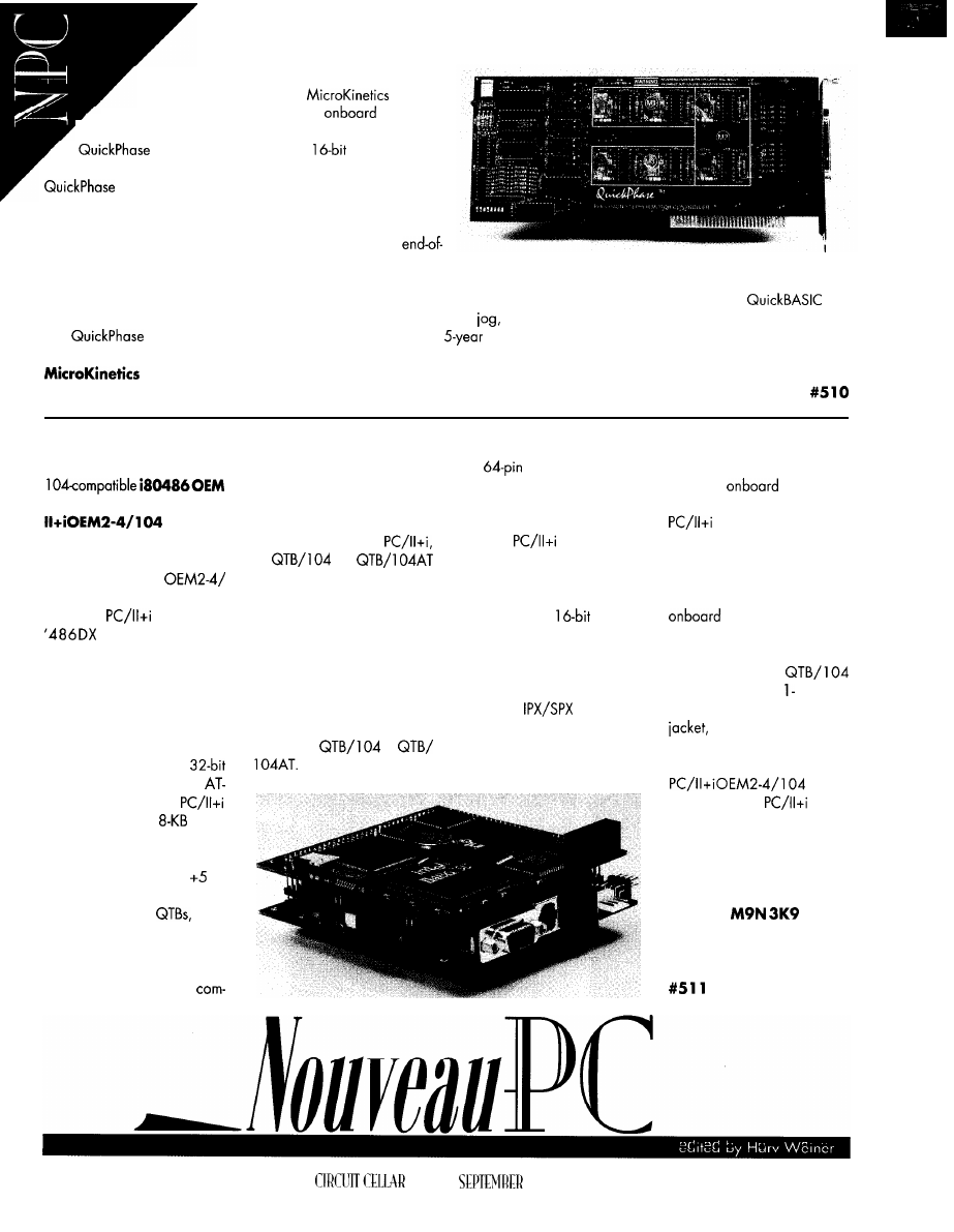
P C - B A S E D M O T I O N C O N T R O L L E R
Quick-Phase
from
is a new
,
stepper-motor controller containing
translators
and power drivers for up to three axes all on one card.
plugs directly into any 8-or
ISA bus IBM or
compatible PC, thereby eliminating the need for external drivers.
is ideal for many applications including scientific
instruments, CAD/CAM modeling, and robotics.
Features of the controller include programmable acceleration
and deceleration, automatic over-temperature protection,
travel detection on all axes, two auxiliary outputs per card, and a
“safety shield open” interrupt.
The software is very easy to incorporate into any application. The subroutine libraries provided support C and
and
include linear and circular interpolation, ramping, keyboard interactive
and electronic gearing.
sells for $339 for 2 axis and $389 for 3 axis. A
parts and labor warranty is included.
Corp.
1220-J Kennestone Cir.
l
Marietta, GA 30066
l
(404) 422-7845
l
Fax: (404) 422-7854
‘ 4 8 6 S I N G L E - B O A R D C O M P U T E R
Megatel announces a PC/
Development Kit.
The
PC/
includes a
single-board computer, break-
out module, and software.
The heart of the
104 kits are the microcomput-
ers. The
features a
p r o c e s s o r o r t h e
‘386SLcompatible PC/II+. Op-
erating at either 25 or 33 MHz,
these boards include Local Bus
SVGA video or LCD controller,
Ethernet interface, SCSI, floppy,
and serial or parallel ports, 2
MB of flash disk, a full
DRAM data bus, and an
compatible BIOS. The
also offers a built-in
cache
with floating-point unit. CMOS
reduces power consumption to
approximately 6 Wand
V.
The PC/l 04 break-out
modules, known as
make
it possible to connect the SBC
to a standard PC/l 04 format.
Connections from the QTB
module to single-board
puters are simplified by the use
of a 96-pin peripheral I/O con-
nector and a 64-pin ISA bus
connector. If the Ethernet op-
tion is installed in the
the
and
can also be connected by rib-
bon cable to the
1
O-pin Ethernet
header. The small PC/l 04 for-
mat lets you add many avail-
able stackplane modules.
All peripheral I/O signals
from the 96-pin I/O connector
are attached to appropriate
peripheral headers or connec-
tors on the
or
All ISA bus signals from
the
ISA bus connector
are converted and connected
to the standard
PC/l 04
bus or
ISA edge connector.
The
Ethernet inter-
face uses the Intel 82595 single
chip Ethernet controller and its
buffered slavearchitecture. The
boards provide
bus op-
eration and are fully 802.3
compliantwith
the
AUI
and TPE
serial interface. Software for
the Ethernet interface includes
full Novell
support.
A complete legal BIOS in
flash memory is provided on
either board. It boots standard
versions of PC, MS, or Novell
DOS. An
ROM DOS
is also offered. As a result, the
runs most popular PC
software packages, including
Windows 3.1. A copy of a
high-performance flash-file sub-
system, which provides the
capability for a 2-MB
solid-statedisk, isalsoincluded.
All OEM/l 04 kits include
t h e S B C b o a r d ,
break-out module, or 2-MB
flash disk BIOS, DRAM, board
ROM, Ethernet, and
SCSI utility software, cable set,
and manuals. The price of the
kit is
$1495 and the
board
is from $1
195.
Megatel Computer Corp.
125 Wendell Ave.
Weston, ON
Canada
(416) 245-2953
Fax: (416) 245-6505
48
INK
1995
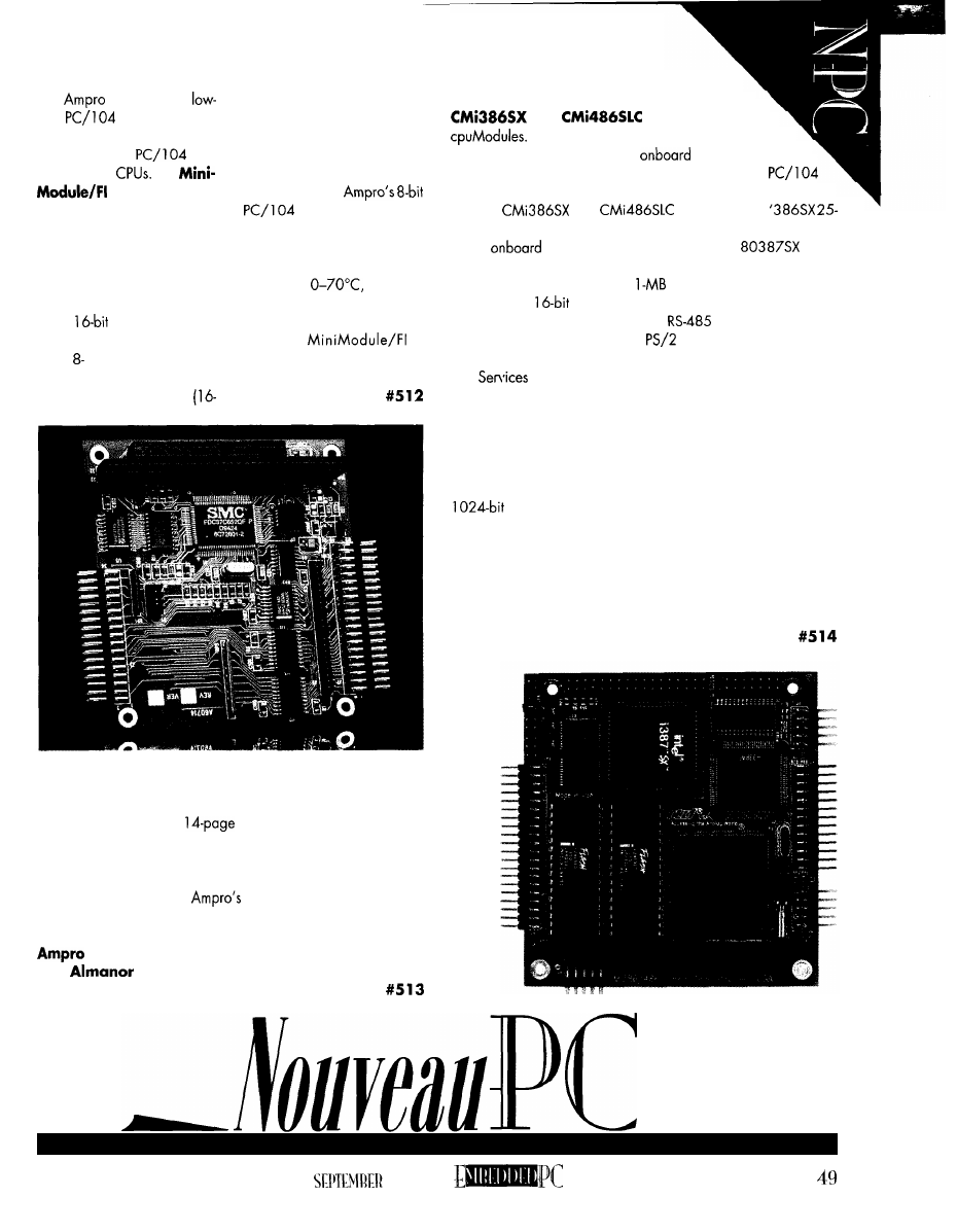
PC/
104 DISK CONTROLLER
introduces a
cost
module that lets
IDE hard disk drives be used
with their 8-bit
em-
bedded PC
The
includes interfaces
for both floppy and IDE disk
drives and is compliant with
the PC/l 04 V.2 specification
for compact (3.6” x 3.8”) em-
bedded PC modules.
The module is equipped
with a
PC/ 104 self-stack-
ing bus, but can be used in
both and 16-bit systems.
Special circuitry is included to
facilitate the use of normal
bit) IDE disk drives in an 8-bit
bus system. The necessary BIOS
support required for IDE drive
operation in 8-bit systems is
included within the standard
ROM-BIOS on
CPU modules. The
module operates from a single
+5-V supply and supports a
wide operating temperature
range of
with ex-
tended temperature ranges
available on special order.
T h e
is
priced at $85 in quantities of
100.
PC/ 104 DESIGN GUIDANCE
Also available is a free white paper called “Designing with
PC/l 04-A Tutorial.” The
tutorial includes an overview
of the PC/l 04 standard, describes how PC/l 04 modules are used
in typical embedded applications, and provides guidelines for
effective and efficient use of PC/l 04 technology. The paper was
written by Rick Lehrbaum,
cofounder and president, who
is generally regarded as the father of PC/l 04.
Computers, Inc.
990
Dr.
l
Sunnyvale, CA 94086
(408) 522-2100
l
Fax: (408) 720-l 305
SINGLE-BOARD COMPUTER
Real Time Devices has introduced the
and
PC/l 04compliant
These fully integrated PC/AT-compatible
single-board computers with an
math-coprocessor
socket reduce the number of modules required for
industrial control and data processing.
The
and
feature an Intel
MHz or TI ‘486SLC 33-MHz processor with programmable clock
rates,
expansion socket for optional
math
coprocessor, 2-MB or 4-MB DRAM installed, and two 32-pin
sockets for 2-MB EPROM or
flash solid-state disk. Also
included are
IDE and floppy disk controllers; one RS-232
serial port; one RS-232, RS-422, or
serial port; bidirec-
tional parallel port; AT keyboard;
mouse; speaker ports; and
a watchdog timer.
and functions provided by the BIOS ensure PC/AT
compatibility. The BIOS also includes SSD support for SRAM,
EPROM, flash memory, NVRAM, and virtual devices. Virtual
device support enables the operator to use peripherals connected
to another PC- or AT-compatible computer without interfacing them
directly to the module’s PC/l 04 bus.
Connection is made through the serial port. A nonvolatile
configuration EEPROM stores the system setup and
provides 5 12 bytes to the user. Direct plug connection to other
modules is made through a standard PC/l 04 stack connector.
Prices start at $578 in quantity.
Real Time Devices, Inc.
200 Innovation Blvd.
l
State College, PA 16803
(814) 234-8087
l
Fax: (814) 234-5218
1995
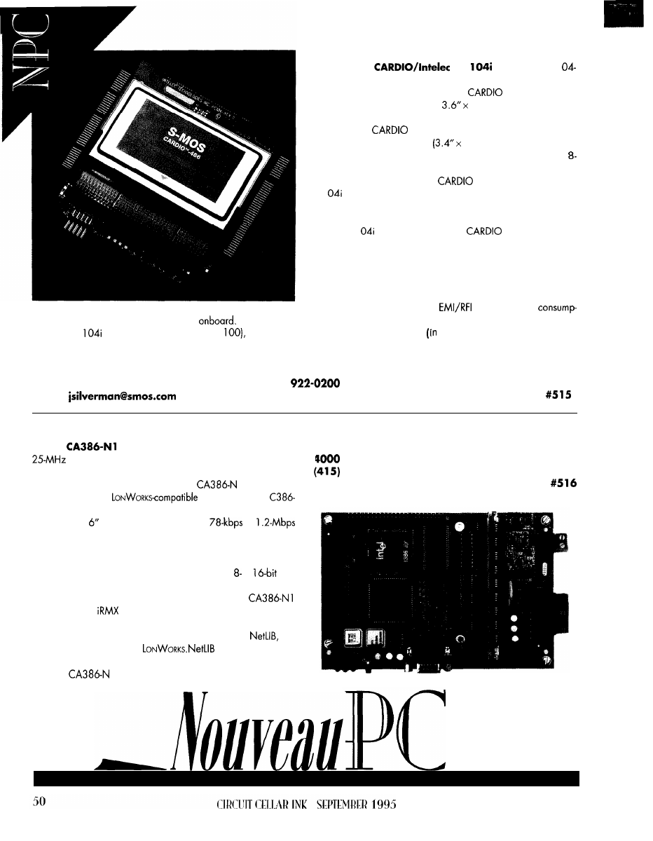
tion with 3.3-V power-supply generation
The PC1
board and the S-MOS
provide two serial
ports, a mouse or keyboard controller, floppy and hard disk
controllers, flash BIOS, an LCD controller, and power-entry connec-
tor. Also available are compatible cables for standard connections,
watchdog capability with an LED indicator, a power-fail indicator,
battery backup, and automatic switchover (external battery re
quired). The system features low
and low power
The PC
starts at $290 (q uantities of
the S-MOS CARD10486 at less than $800
q uantity), and the ‘386 version at
less than $400 (in quantity).
SMALL PC/l 04 MODULE
The S-MOS
PC
board is a PC/l
compatible single-board computer. This board enables the user to
combine the small-size advantage of the
with the stackable
PC/l 04 peripheral products. The
3.8” board meets the one
stack mechanical and electrical PC/l 04 Rev. 2.2 specifications.
The S-MOS
is a fully functional IBM PC/AT computer
about the size of a credit card
2.2”). Versions are available
that include the Intel ‘386 or ‘486SL and Chips and Technologies
bit 8680. Upgrading from an ‘x86 to a ‘386 or ‘486 is easily
accomplished by replacing one
module with another. The
PC1
is a small, PC-compatible single-board computer that
achieves more functionality and a greater choice of peripherals,
software drivers, operating systems, and application libraries.
S-MOS Systems, Inc.
2460
North First St.
l
San Jose, CA
95131
l
(408)
l
Fax:
(408) 922-0238
E-mail:
NETWORKED EMBEDDED PC
The
from Coactive Aesthetics pairs the powerful
Intel ‘386EX processor with Echelon’s 3 120 Neuron for
peer-to-peer networkcommunications. The 3 120 running Echelon’s
MIP program and Coactive’s libraries lets
1 applications
access data on any
node and lets the
N 1 act as an embedded “compute engine” for the network.
The 4” x board is available with
or
twisted-pair transceivers. The system includes 256 KB, 1 MB, or 4
MB of RAM and 5 12 KB of flash memory. It has eight digital I/O
lines, three programmable counter/timers, two RS-232 serial
ports, and an optional battery-backed RTC. The or
PC/
104 interface offers expansion with industry-standard peripherals.
The OEM Software Development Kit for the
includes Intel’s
real-time OS in flash along with utilities for
downloading and running programs. Programs are compiled on a
PC using Visual C. The package includes Coactive’s
a C
library for interfacing to
lets users declare
network variables and use them to communicate with other nodes.
The
1 sells for $699 in single quantities.
Coactive Aesthetics, Inc.
Bridgeway, Ste. 303
l
Sausalito, CA 94965
289-l 722
l
Fax: (415) 289-1320
E-mail: coactive@coactive.com
PC/l 04
CARD
IBM has added a
card to its line of
prototyping cards.
PC/l
layer raw card with internal power and ground planes.
Features include a 0.1 grid of plated-through holes of
0.04” diameter for component or socket mounting,
peripheral power buses, and fanned-out signal connec-
tion from the J 1 and connectors. The connectors are
installed and nylon standoffs are included.
The card is in stock at Marshall Industries and is
available from Bell Industries ond Bell Micro Products
Distributors. The single-quantity price is
$1 10.
IBM Corp.
Microelectronics Div.
1701
St.
NY 13760
(607)
Fax: (607) 755-6562
The
is a shortcut to a
custom-designed controller. It is a
C-programmable microprocessor
core with memory, supervisor,
DMA
,
and clock built in. All you do
is add interface and control logic.
Call our
916-753-0618 from
your
FAX
. Ask for data sheet
1724 Picasso Ave.
Davis. CA 95616
FAX
REMOTE POWER CARD!
RESET
CHAN ADC
FILES
2 CHAN DAC
5 YEAR LIMITED WARRANTY
F R E E S H I P P I N G I N U S A
52
CIRCUIT
INK
1995
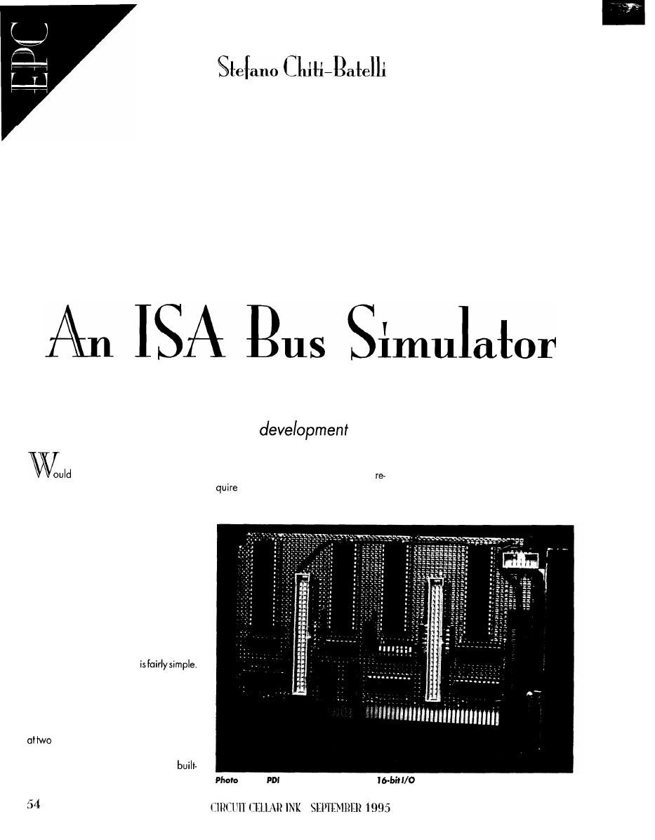
You could simply plug in your prototype. However, design flaws can prevent
operation or cause permanent damage. Stefano’s ISA bus simulator gives the
engineer more control over the
and test process.
you like to develop an interface
board for the ISA bus?
Here’s a solution to your needs-the
PDI (Prototype Development Interface), a
full-featured ISA bus simulator that should
help you understand and test the inner
workings of the most common type of PC
expansion boards.
The PDI ISA bus simulator consists of
two separate boards: a fairly simple I/O
expansion board for the PC (PDI internal
module) and an external module. The ex-
ternal module relies on the internal board
for its power supply and I/O control lines.
Software controls simulator features.
Operating thesimulator
First, you plug the to-be-tested-board (TBTB)
into the slot provided by the external PDI
module. Next, you run the PDI debugger to
test the TBTB.
With the debugger, you can operate
different levels. You can set the status
(high or low] of every single line of the ISA
bus or you can take advantage of the
in macro function to automate repetitive
and/or tedious tasks which otherwise
The debugger itself takes advantage
manual control of many different bus
of this feature. For example, normal I/O
lines (e.g., read and write cycles).
operations on the ISA bus (e.g., input from
1: The
internal module offers a
expansion board of up to 96 lines.
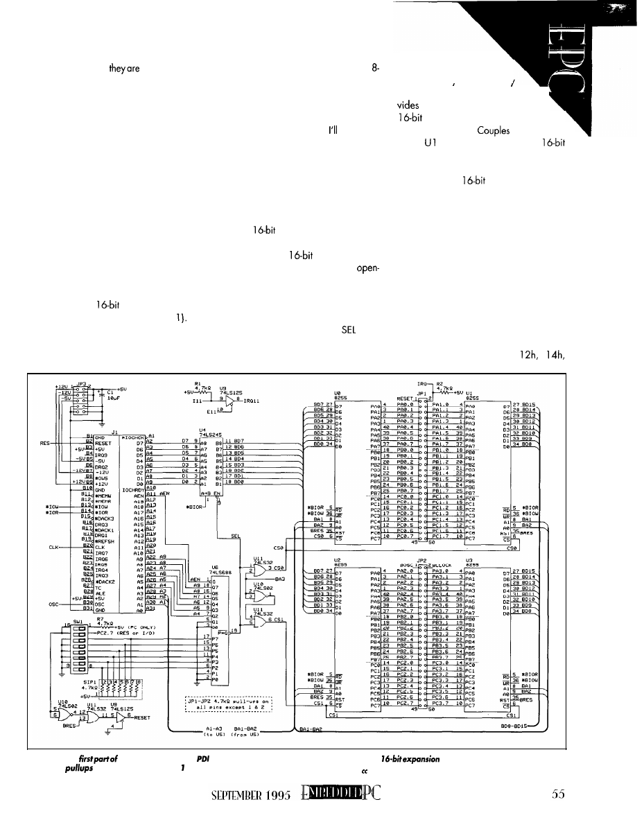
or output to I/O ports) aren’t hard coded in
thesoftware. Instead,
implemented
via macro functions which can be easily
modified using any ASCII editor.
The
PDI
internal module is essentially
a digital I/O expansion board, hosting
four 8255 chips for a total of 4 x 24 = 96
I/O lines. These boards are commercially
available (approx. $100). If you are will-
ing to apply the small modifications needed
to connect to the PDI external module
(power supply lines and a couple of “spe-
cial” lines such as RESET), you can skip the
soldering required for the internal module
and concentrate your efforts on the exter-
nal module. The software should be easily
adapted to slightly different hardware.
I N T E R N A L M O D U L E
As mentioned, the PDI internal module
is a fairly simple
expansion/inter-
face board for the ISA bus (see Photo It
provides the I/O lines needed to interface
to the external PDI module. You need 64
(65 if you want manual RESET) I/O lines.
This number can be lowered if you reduce
the features of the PDI so it only accepts
bit ISA boards in its simulated slot (see later
discussion).
The schematic of the internal module is
provided in Figure 1. Since you can buy a
functionally equivalent board, only briefly
describe this board. The simulator software
takes the possibility of using a different PDI
internal module into account-all I/O op-
erations are performed by a limited num-
ber of routines.
The interface board is a 16-bit ISA
expansion board. As such, it uses the 1016
line on the
extension connector to the
ISA bus. This line serves as input to the PC
and is shared by all
boards plugged
into PC slots. Although it could be
collector driven or tristated, I chose to use
tristated.
Chip U6 compares addresses with the
value set by DIP switches (switch closed =
low address bit). Its output line
is the
main activation switch for the rest of the
circuit-when low, it’s your turn!
Since the board is
16 bit and the 8255 chips
are only 8 bit, thev obviouslv
work in pairs. One gets or pro-
\
data for the lower byte of the
word, while the other chip works
with the upper byte.
are
formed by
.
UO +
and by U2 + U3. I use
interfacing because I want to be able to
switch (i.e., update with a new value) the
whole simulated
data bus in a single
write operation. Using a commercial 8-bit
board sacrifices this option.
Each 8255 needs four addresses, so
we need a total of sixteen addresses to talk
to our board. In compliance with the space
reserved by IBM for prototype expansion
boards, possible I/O base addresses are
all even values between 300h and 3 1 Oh.
I chooseaddress 3 1 Oh, which I use through-
out the rest of this article.
Remember, since our board is 16 bit,
we only reference even addresses. For
example, with a base address of 3 1 Oh, we
address I/O ports at 3 1 Oh, 3
3
Figure la: The
the schematic of the
internalmodule shows the 8255s. Since it is a
board, the 8255s work in coupler.
The 4.7-k
are on all pins except and 2, and bypass capacitors are between V and Gnd of each chip.
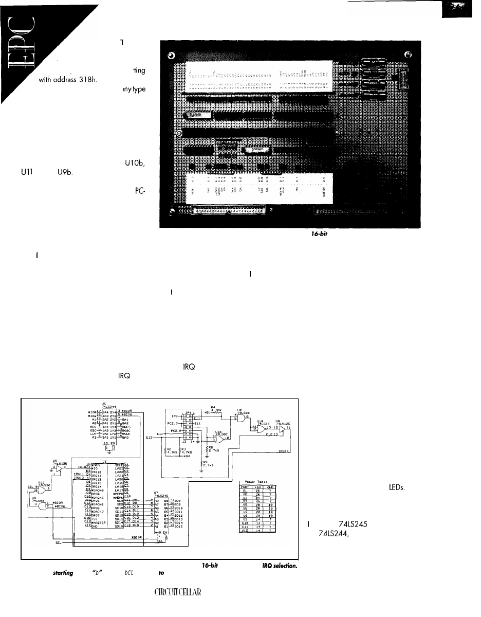
and so forth.
pair of 8255s uses
eight I/O addresses,
second pair is referenced
Reset is a useful feature of c
‘he first
the first
so the
star
of equipment. In this case, it is useful to:
a) manually drive the RESET line of the
simulator slot and
b) automatically perform a power-on reset
whenever the PC is turned on
Reset is accomplished by gates
d, and
Since a manual reset
requires use of an I/O line, DIP switches
can disable this feature, reverting it to a
only reset with no user activation.
Apart from I/O lines and reset, the
connectors have pins for the real bus lines
CLOCK and OSC. The external module
provides jumpers so you can choose to
connect real or simulated signals to the
TBTB. have done this, though some picky
TBTB boards might mind if their clocks
aren’t fast enough.
last but not least, the internal PDI
module provides two kinds of support for
interrupts: externally activated or locally
activated. The latter occurs most frequently
in the case of 8255 chips being used in a
mode other than Mode 0 (see 8255
datasheet). This use probably means that
the PDI internal module is not used in
conjunction with the external module, but
for another kind of task. The externally
activated interrupt refers to the
line,
which comes from an external device.
Photo 2: The PDI external module holds the simulated
ISA slot.
Jumpers enable or disable the interrupt
sources.
Since they aren’t used for the simula-
tion, you might wonder why put these
interrupt features in the PDI internal mod-
ule. wanted to design a general-purpose
I/O expansion board, however I wanted
to provide additional features. Since I did
not need all 96 I/O lines, I designed for
future applications that might include simu-
lating or simply talking to the digital inter-
face the TBTB board provides.
In this scenario, an interrupt feature
[i.e., the
line or a special configuration
of the fourth 8255) is a valuable addition.
If required, jumpers are provided to enable
Figure 1 b: The second part of the PDI internal module includes the
bus signals and
Line names
with a
(e.g.,
K)
refer buffered lines.
5 6
INK SEPTEMBER 1995
selected interrupt sources. These sources
can be connected to interrupt channels 1 1
or 12 of the ISA bus.
Since we aren’t using all 96 I/O lines,
the free ones might be used for other
simulation or interfacing tasks. For ex-
ample, suppose you want to develop an
LCD interface board for the PC. The PDI lets
you simulate not only the ISA bus, but also
the LCD itself, though only after a little
extension of the software to allow control of
the extra (above the “first” 64) I/O lines of
the 8255s.
Since an external board may require
a nontrivial amount of power, connect Gnd
and Vc, (see the power supply flat-cable
connector) to all contacts of the ISA bus
which provide them. The PDI external
module has fuses on all power lines.
E X T E R N A L M O D U L E
The PDI external module is shown
in Photo 2. I used a double-Eurocard-
sized prototyping board. Apart from
the 16-bit ISA slot and the flatcable
connectors, the big show (literally) is
provided by the many flat
They
are powered by buffers which connect
them to the
ISA
bus lines (see Figure 2).
Since its pin ordering is more regular,
used the
chips, instead of
the
as LED current buffers.
With careful placement of the buffer
chips and connectors [and perhaps
use of the 245’s DIR line), you can wire
the simulated bus lines of the external
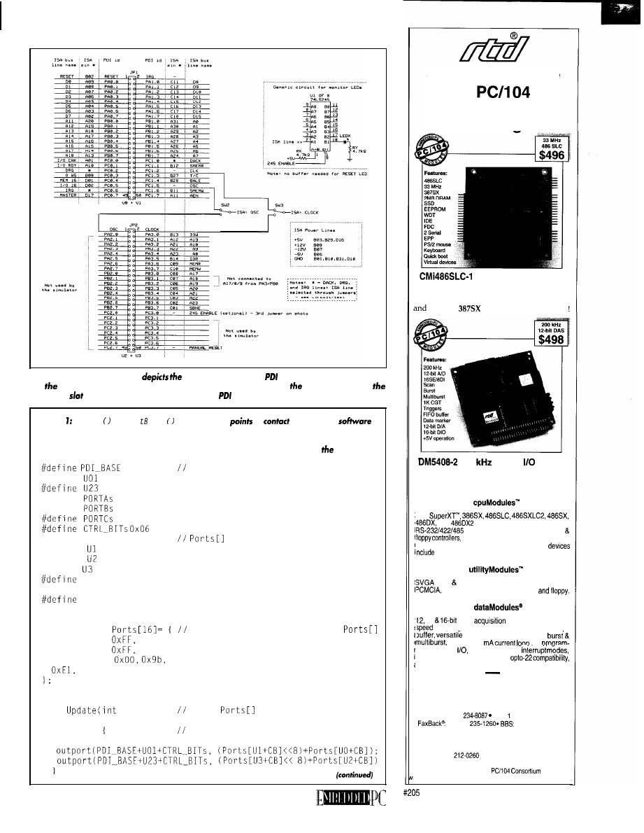
Figure 2: This partial schematic
main sections of the
external module. Not shown
are
fuses for power-supply connections and resistors between
data bus lines of
simulated
and the corresponding lines of the
internal module.
Listing
Update
and Ge i t are two of the
of
between PDI
and hardware. Should you decide to use a commercially
available 8255 board, you’ll
probably have to modify these (and other) routines according to the board documenta-
tion. Various hardware access #defines are shown to help you decipher
code.
0x310
IO base address
#define
0x00
0x08
#define
0x00
#define
0x02
0x04
#define UO 0
vector access defines
#define 4
#define 8
#define 12
PA 0
i/define PB 1
PC 2
#define CB 3
unsigned char
8255 registers are read-only
0x00, 0x00,
0x99,
//holds the last written values
0x00, 0x00,
0x90,
0x00, 0x00,
0x80, 0x80, 0x80,
void
flag)
write
to the 8255s
if (flag)
if flag is set then also a 'mode'
change
SEPTEMBER 1995
Sets
the
Pace
in
CPU and DAS
Technologies
Fully Integrated PC-AT
with Virtual
Device
Support
When
placing your order, mention this ad
receive a
math coprocessor FREE!
200
Analog
Module
with Channel-Gain Table
Make your selection from:
9
XT,
and
processors. SSD, 8MB DRAM,
serial ports, parallel port, IDE
Quick Boot, watchdog timer, power
management, and digital control. Virtual
keyboard, video, floppy, and hard disk.
7
CRT LCD, Ethernet, keypad scanning,
intelligent GPS, IDE hard disk,
18
14
data
modules with high
sampling, channel-gain table (CGT). sample
triggers,-scan, random’
DMA. 4-20
bit
mable digital
advanced digital
incremental
encoder
interfaces,
and power-down.
&Real Time Devices USA
200
Innovation Boulevard
l
P.O. Box 906
State College, PA 16804-0906 USA
Tel: 1 (814)
Fax: (814) 234.5218
1 (614)
1 (814) 2349427
RTD Europa
RTD Scandinavia
Budapest, Hungary
Helsinki, Finland
Fax: (36) 1
Fax: (358) 0 346.4539
RTD is a founder of the
and the
odd’s leading supplier of PC1104 CPU and DAS modules
57
via
nts, thus
let
you qui
or low
ine. You c
the schematic so each LED turns
flat-cable
speeding
judge
(LED off)
an modify
on only if
the corresponding line is in its on state
(usually a 0 value). This modification
quiresthe use of
inverters
or
connection
of
these
between buffer output and
instead of Gnd. However, it is my experi-
ence that the current way of functioning is
consistent and requires little time to adapt.
Please note that the use of flat
is
recommended since spacing between the
ISA slot pins is only 0.1”. Adjacent
must fit or you have to place the
in two
columns.
As a general rule, LED color indicates
the bus line: data (red), address (yellow),
and control (green). Exceptions to this rule
include the RESET and DRQ lines and the
“fuse-not-burned”
for
12 V, and
-5 V. In total, you need 20 red, 22 green,
27 yellow
Figure 2 offers detailed information
about flat-cable connector pin use
W O R L D ’ S S M A L L E S T
DX
The
PC/II
includes:
continued
+
+
+
+
+
+
ing the flat-cable connectors found on the
PDI internal module) and ISA bus lines.
Also included is the typical simulated ISA
line (buffer and LED). A special case is
provided by data bus lines, or optionally
by each ISA line which can be either input
or output, depending on bus condition
(notably the MASTER line).
These bidirectional lines might require
special attention since
(or even the
simulator software) might not function prop
erly. It might happen that one or more of
these bidirectional lines can be driven by
both the simulator and the TBTB in two
different states! Therefore, a resistor of
approximately 330 placed between
each PDI and ISA bus line helps reduce
hardware damage by limiting current.
Embedded PC with
ting Point,
Ethernet Super
VGA Only
l
CPU
or
clock frequency
l
Point
l
Ethernet
local
Area
Network
l
l
l
4 or 16MBytes User DRAM
l
adapter)
l
powerconwmptian
and Flash are registered trademarks of
Corp.
as
PC, AT of
of
Computer
125 Wendell Ave.
l
Weston, Ont.
l
l
Fax: (416)
l
l l l l l l l l
Not all ISA lines of the simulator slot
have an LED since decided to only support
one interrupt channel and one DMA chan-
nel. However, these lines aren’t fixed.
ersareprovided.Youcanchoosetoconnect
to any possible INT or DMA line.
Unused input lines are pulled up. The
corresponding to INT and DMA are
placed in correspondence to a related line
and
which is near
the configuration jumpers (see Photo 2).
Since TBTB insertion and extraction
can require considerable force, don’t for-
get to place supporting hardware. By do-
ing this, you won’t be as likely to bend the
slot-holding board.
Though not shown in Figure 2, fuses
should be placed [along with power-moni-
toring
on each power-supply line.
Possible generous values could be 2 A
V), A
V), and 0.5 A (-5 V). The
figure for
V includes current needed by
the PDI external module itself (buffers and
T H E S O F T W A R E
The simulator software is written in
Borland C. It compiles to a DOS program
with an old-style interface similar to DOS.
You type in commands which get inter-
preted as soon as you hit Return.
Before commenting on a couple of
core routines, let me briefly discuss the
overall operation. As mentioned, you can
control each simulated bus line individu-
ally. For example, the command
forces the
line (address enable) low.
Format is somewhat flexible. A space can
replace the = or you can use lower case.
You can also check the status of each
line. For example, the command
MASTER
shows
current high or low status of the
corresponding bus line. If the involved line
is an output (and as such it is controlled by
the PDI hardware), you see the last written
value, not its actual voltage. The two values
might differ with a hardware malfunction
(i.e., TBTB or PDI failure). This difference
CIRCUIT
INK SEPTEMBER
1995
Listing 2: The Get
i
routine gets the next command from either the keyboard (or
a DOS pipe) or the currently executing macro file. Please note the use of the DOS
(Buffered Keyboard Input) function call. This call lets the
program take advantage of
any
T-like utility you may have
in your system.
Input line buffer: this data structure uses a DOS call which
handles line input and is compatible with
DOSKEY, etc.
typedef
unsigned char
size:
unsigned char
got;
char
BuffKeybInp;
int
quit = 0;
int
= 0;
int
= 0:
char
=
char *CmdPtr;
char
set if exiting from simulator
set if executing a macro
of ms to pause
the (default) command line
its pointer
char
=
FILE *MacFile:
char
BuffKeybInp
union
REGS
regs;
char
tc;
if
i f
EndMacroO;
end of macro file
*CmdLine = 0:
if
!=
EndMacroO;
error in macro file
*CmdLine = 0:
discard
char
if
EndMacroO;
if
i.e. if not auto-startup
of macro!
*CmdLine = 0;
else
not
at end of macro
i f
=
! = N U L L )
i f p a r a m e t e r s
tc =
‘1’ or ‘2’ (parameter number)
* L i n e = 0 ;
C m d L i n e ,
?
L i n e ) :
else
not
executing a macro!
L i n e B u f f . s i z e =
1 :
L i n e B u f f . g o t = 0 ;
= 0 x 5 5 ;
=
B u f f e r e d K e y b o a r d I n p u t
= ( u n s i g n e d )
Your Complete
x86 Solution!
Multitasking in Real and
Protected Mode
Full-featured, high-perform-
ance.
kernel. Custom-
ized to
for
demanding applications. Real
mode works stand-alone or with
DOS.
segmented protected
mode works with
or
286 I DOS
flat
protected
with
or TNT.
Protected Mode Environment
or
protected
mode entry,
services.
application loaders,
and
support.
DOS-Compatible File System
Full-featured file
manager, IDE, floppy, and
drivers available.
Dynamically
Modules
Runs independent
as tasks which may
be downloaded or loaded from
disk.
Networking
stack. Fast UDP.
Packet driver interface. NE2000,
SMC, and SLIP drivers available.
Task-Level Debugging
Provides tracing and
symbolic debugging. Works with
or without code debuggers.
C++
Classes
Class library built upon
smx. Provides fully
ible kernel interface.
Extended Memory, Real Mode
Allows copying data
between real memory and extend-
0
ed memory buffers or accessing
extended memory via a window.
User Interface
Text windowing.
Dresses up user interfaces.
Low Cost Easy to Use
Royalty-free licenses. Supports
common, low-cost C compilers and
debuggers. Great manuals. Source
code available.
Reliable
On market 6 years. 100’s of appli-
cations. Extensive error checking
free trial.
l-800-366-2491
MICRO DIGITAL, INC
714-891-2363 Garden Grove, CA USP
714-893-5118
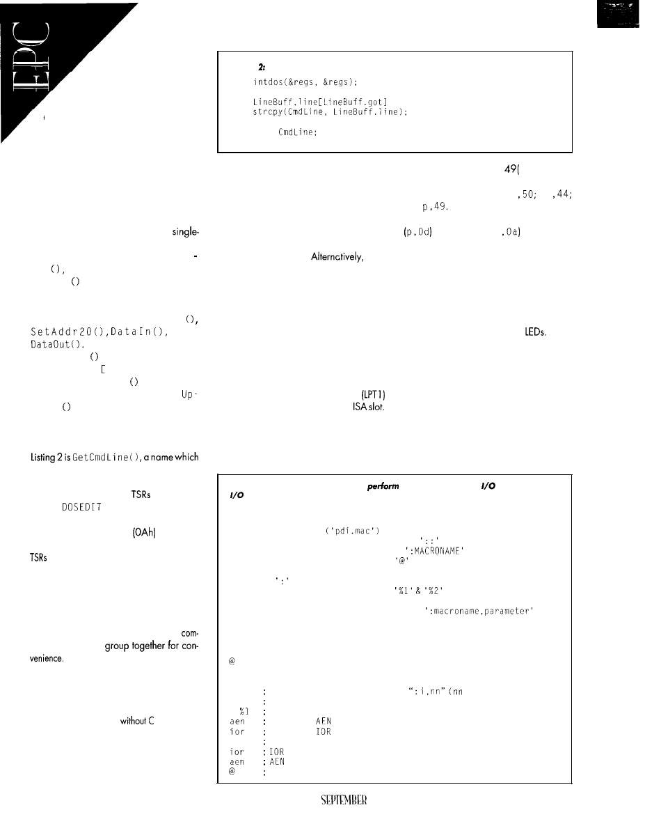
can probably be seen
from the LED status.
Help is provided as a list
of supported commands with syn-
tax. There are other commands con-
trolling features apart from bus lines.
Please note, however, that only basic
features are directly supported by the soft-
ware. While you can read and write
memory or I/O (by hand or with the pro-
vided macros), more complex cycles such
as DMA or MASTER cycles are not sup-
ported at a high
level. In other words, you
can perform these cycles, but you have to
manually control the simulator (via
line commands) or write your own macro.
The lowest-level routines are Up
date
shown
in Listing 1, and
Get B i t
Eventual software conversion
to different I/O expansion boards (PDI
internal module) will probably also require
modifications to the routines Set Data
a n d
L. pd a t e
transfers new output data
from the Ports 1 array to the 8255
registers, while Get B i t
reads the data
lines declared as input. A flag in
date
tells whether to also update the
8255s’ mode registers (see the “Modifica-
tions” section).
Another important routine included in
fully describes its task. For line editing and
command history retrieval, this routine can
take advantage of system
such as the
popular
utility (but not DOSKEY,
sorry!). The routine uses the Buffered Key-
board Input DOS function
to get user
commands. It all works since many of the
hookthemselvestothe DOS function,
thus expanding its capabilities.
M A C R O S
In my opinion, thenicestfeatureofthe
simulator
is
its macro support. Macros are
simply a collection of consecutive
mandswhich you
Listing 3 shows what a typical
macro file looks like. Also shown is the
"read from I/O port" macro, one of the
most-used macros.
Macros
let
you easily extend the fea-
tures of
the
simulator
coding. C
is only necessary if you decide to extend
the simulator's command set. For instance,
you mightwantto support macro nesting,
looping, or (conditional) branching.
60
Listing continued
= 0x00;
return
Each macro can accept up to two
parameters of either text or numbers. With
text, they cannot hold commas (since com-
mas separate macro parameters), and with
numbers, they must be expressed in hexa-
decimal notation.
The simulator can execute a macro
command at full speed.
each
macro command can execute after a fixed
delay (e.g., one command per second) or
be single stepped (by pressing Return).
H E R E W E G O
We’re finally ready for a test run of the
simulator. Included with the default macro
file
(PDI .MAC) are a couple of macros
which can be used to printcharacterson a
printer. The printer should be connected to
the PC via a parallel interface board
which is inserted into the simulated
The first macro (pi n i t) initializes the
printer. Next, the p macro prints each
single character to the printer. For ex-
ample, since
the
c h a r a c t e r s “ P D I ”
are ASCII 50, 44, and
hex), these
values are given as parameters to three
consecutive p macro calls: p
p
and
Don’t forget to send carriage return
and line feed (p
characters.
Laser printers also like a form feed (hex Oc)
to force them to eject the printed page.
M O D I F I C A T I O N S
Modifications and improvements are
obviously possible. You may simplify the
project by only simulating an 8-bit bus or
decide to reduce or eliminate
I can also suggest hardware changes
which would
help
you avoid some inconve-
nience caused by a peculiar characteristic
of the 8255 chip. Let me explain.
Imagine you programmed an 8255
(I’m talking about Mode 0) so port A is
configured as an 8-bit output port. Port A
could be changed from output to input and
then, having performed some input task,
back to output. Unfortunately, as soon as
Listing 3: A macro may be used to
i n p u t o p e r a t i o n s f r o m
p o r t s . T h e “ I n p u t
from
port” macro is commented assembly sty/e. Please note
this commenting is not
allowed
in a real macro file. I do it here to clarify macro command interpretation for you.
default macro file
for pdi.exe
first line of a macro file must be
each macro starts with a line =
(case is ignored!)
each macro ends with a line =
free comments are allowed between macros
macro
is special as it is automatically executed at startup
macros may have 2 parameters:
in the macro text.
To invoke a macro with a parameter:
Please note that parameters are separated with commas!
Special startup macro (may be modified as you need)
Input
:i
di
a
0
0
d
1
1
from I/O port
name of macro, invoke with
is address in hex)
declare data bus as input
set address bus to value of macro parameter
activate
line
activate
line
read data bus
inactive
inactive
end of macro
CIRCUIT CELLAR INK
1995
you write a new value into the 8255 mode
register, even if it is exactly the same (e.g.,
an output port as output), a
data port declared as output loses its output
values! Obviously, you can quickly repro-
gram the output register, but you still get an
output glitch on the lines.
In our case, this relatively small prob-
lem happens when we switch direction of
the data bus, thus requiring an 8255 mode
change. Since the PDI internal module is a
board, two 8255s are involved, so
a potential maximum of 48 output lines
undergo this glitch. Of course, the situation
is typically not so tragic, and I haven’t seen
any serious problem while testing the PDI.
Nevertheless, if you want to be sure
that this cannot cause any problems, the
only solution is to use two lines-one for
output and one for input-for every bidirec-
tional bus line.
You also need a tristate buffer be-
tween the output line and simulated bus
line. That way, you never have to repro-
gram any 8255 mode register, but you do
have to control the tristate buffer (with a
common line), thus further increasing the
number of required I/O lines for the simu-
lator!
From a software point of view, porting
to Windows would be the biggest modifi-
cation. Windows would offer fancy things
such as graphical simulator status indica-
tion (you could use colored buttons which
mirror LED status changes), line control via
mouse clicks, and so on.
leave the special flare to you as you
build your own PDI.
has been involved in
personal computer and microcontroller
programming for years. His experience
ranges from pinball machines and video
games to
control systems. Sfefano
is current/y completing a degree in math-
ematics.
REFERENCES
Nisley, Ed. “Blindsided
Embedded Firmware
INK,
31, Febru-
ary
Edward. AT Bus Design. San Diego:
Annabooks.
416
Very
Useful
417
Moderately Useful
418 Not
Useful
Your Embedded System
Designs!
If your embedded
system applications
require PC-like
functions, i.e. GUI,
networking, mass
storage, standard operating
systems, and off-the-shelf software,
consider using the PC architecture as a
macrocomponent.
Let us show you how.
Call l-800-966-5200 today.
Proven Solutions for
Embedded Control
the PC architecture
that fits in the
palm of your hand
9 9 0
A v e n u e
S u n n y v a l e , C A 9 4 0 8 6
Byte Craft
l
Fast, efficient optimizing compilers
l
Chip specific
l
Built-in assembler
l
Integrated Development Environment
l
Linker, librarian
We respond to your
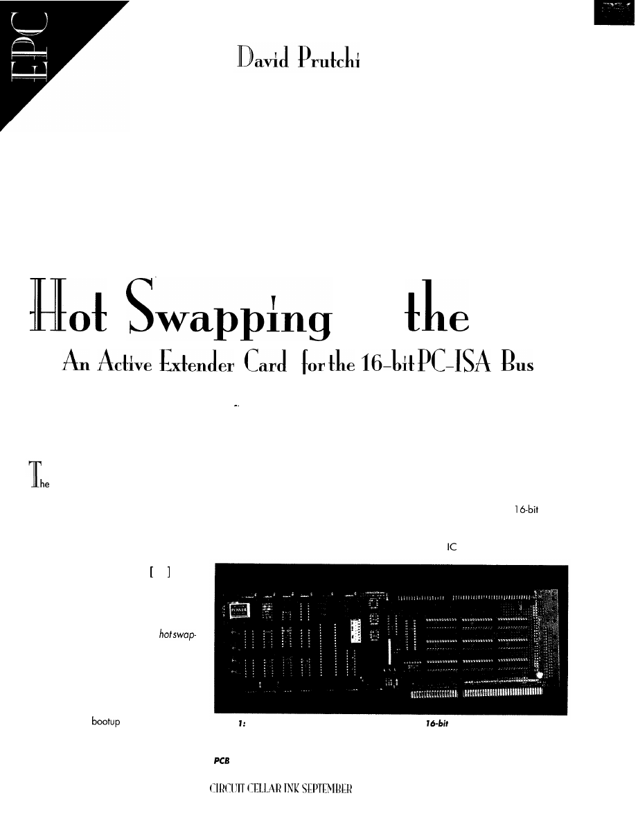
on
PC
Nothing is worse
than powering the motherboard up and down to test a
development board Design flaws at best can prevent operation and at worst
cause permanent damage. Join David in looking at a safer, faster solution.
thing that annoys me the most when
testing and debugging an add-in card for
the PC is the constant need for powering
the computer up and down to reconfigure
jumpers, make circuit changes, and repo-
sition probes.
Standards are being developed un-
der the Plug-‘n’-Play philosophy
1
which
let users remove and replace add-in cards
and peripherals while a PC is fully pow-
ered without damaging the added hard-
ware or the computer. Software standards
are also being introduced so that
ping, as this procedure is commonly known,
does not crash the system.
Until a safe hot-swapping standard is
widely accepted and implemented, test-
ing, debugging, and configuring add-in
PC cards involves incessantwaiting-again
and again-for
and program ini-
tialization unless, of course, you experi-
ment with the hot-swapping extender card
(see Photo 1) described in this article.
62
Through a relatively simple hardware
The hot swapping extender card uses
arrangement, it is possible to safely hot
high-speed solid-state switches to connect
swap an add-in card on any PC. All you
the digital signal lines of the
PC-ISA
need is a means of isolating the PC’s data,
bus to the add-in card under test. Power
power, address, and control lines from
lines are also switched in the card, and a
those of the add-in card under test.
specialized safeguards the computer’s
Photo The hot-swap extender card fits in a standard
ISA slot, while the add-in card
u n d e r t e s t s i t s o n top of the extender card. Hot-swapping with the extender card
i
s
a
s
w
i
t
h
o
u
t
w o r k s w e l l f o r
is available for systems where timing
i
s
c
r
i
t
i
c
a
l
.
1995
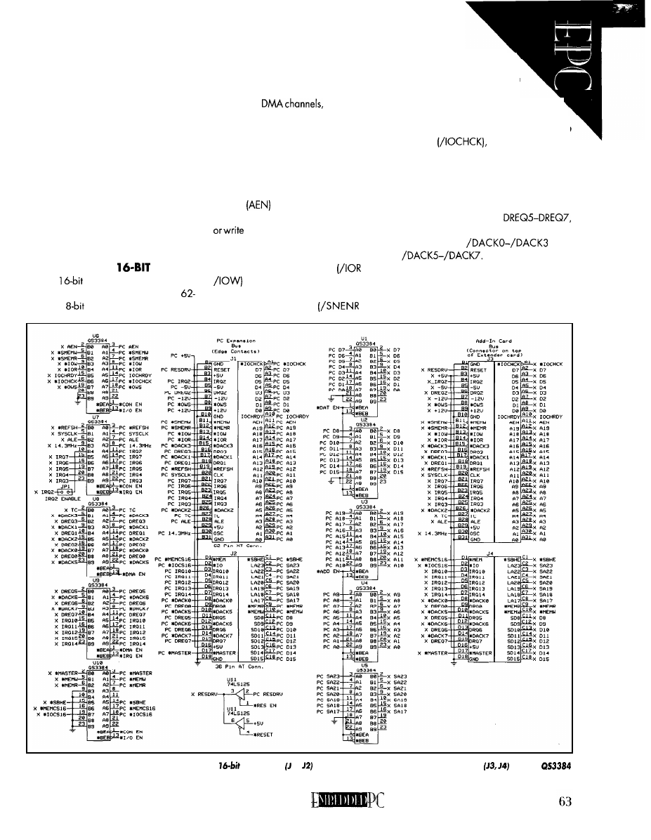
supply from power transients during a hot
swap.
To hot swap this extender card, simply
press a push-button switch to power the
add-in card down and up again without
causing the computer to crash. Timing
logic in the extender card connects or
disconnects the logic and power lines in a
sequence that ensures the add-in card can
restart its activity after being replaced on a
fully operational computer.
Alternatively, the operation of the ex-
tender card may be controlled through
software. Toward the end of this article, I’ll
show you how to use this feature to imple-
ment a highly automatic test setup.
S W I T C H I N G T H E
I S A B U S
The
Industry Standard Architec-
ture (ISA) bus comprises the original
contact,
bus of the PC/XT and an
extra 36-pin connector to carry the addi-
tional signals available for system expan-
sion when the PC/AT was introduced. A
total of 16 data lines, 27 address lines, 1 1
interrupts, 7
and an assort-
ment of control lines and power buses
make up the 98 pins of the full ISA bus.
During a typical transaction between
the PC and an add-in card, the PC issues an
address which, depending on the type of
data exchange, is validated through either
the address latch enable (ALE) or address
enable
lines. The issuing of a valid
address is accompanied by either a read
signal through which the processor
or DMA controller communicates to the
add-in card the direction of data transfer.
I/O read and write signals
and
indicate that data is to be trans-
ferred to or from the data bus. Memory
read or write signals
and
/SMEMW) indicate
CPU or DMA controller
need a data transfer to or from
main memory.
The add-in card issues hand-
.
shake signals to the motherboard to
indicate parity error states on an I/O
channel
request the insertion
of additional wait states (IOCHRDY), and
request completion of the current bus cycle
without additional wait states (/OWS).
For DMA transactions, the add-in card
requests access to DMA devices through
lines DREQO-DREQ3 and
while the PC acknowledges such requests
through lines
and
The PC issues a high
pulse on the TC line when the terminal
count for a DMA channel is reached. In
addition, the /MASTER signal can be used
in combination with a DRQ line by add-in
Figure I: The data, address, and control lines of the
PC ISA bus 1,
are switched on and off the add-in card‘s bus
through
high-speed CMOS analog switches.
SEPTEMBER 1995
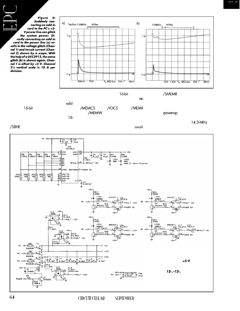
C h l
1 . 0 0 ”
Tek Run:
C h l 5 0 0 m V
boards to take control of the bus through a
eight data bits are used. A
access to
able to
and /SMEMW.
DMA channel.
memory locations or I/O locations is
The other signals available in the bus
To provide compatibility with XT
quested by the add-in card through the
are used for system-wide control. RESDRV
in cards,
data exchange between
16 and
16 lines.
is a reset driver signal used to reset system
the motherboard and an add-in card can
and
on the 36-pin connector
logic at
or as a response to a
take place either as two 8-bit or a single
indicate to the processor that the add-in
power bus fault. The SYSCLK line carries
bit transfer. The system high-bus enable
card needs memory access to the full 16
the system clock, while the
line
line is pulled low when the upper
MB, rather than to the l-MB access
carries the system-oscillator signal to the
Figure 3: A programmable electronic cir-
cuit breaker provides
power man-
agement to enable hot-swapping without
causingcatastrophicgliichesonfhepower
bus. The +
and -5-V lines are
protected through self-resetting fuses.
Overcurrent states on any of these lines
cause the automatic disconnection of the
add-in card from the PC bus.
INK
1995
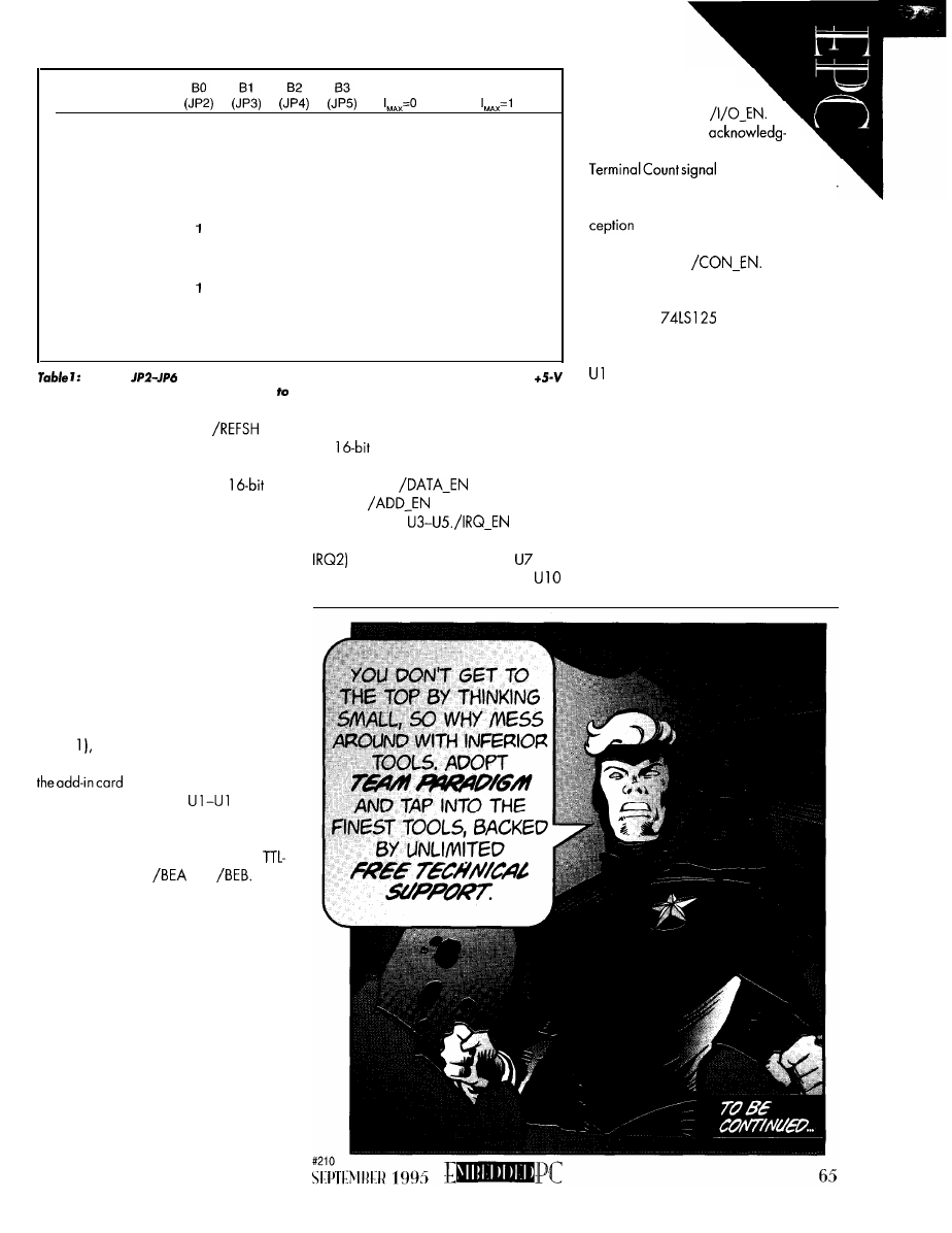
Trip current [A]
(typical)
0
0.25
0.5
0.75
1.0
1.25
1.50
1.75
2.0
2.25
2.50
2.75
3.0
Max. output current [A]
(JP6)
(JP6)
0
0
0
0
1
0
0
0
0.02
0.02
0
1
0
0
1
1
0
0
0
0
1
0
1.25
1
0
1
0
1.5
0
1
1
0
1.75
1
1
0
2.0
0
0
0
1
2.25
1
0
0
1
2.50
4.0
0
1
0
1
2.75
1
0
1
3.0
0
0
1
1
3.25
1
0
1
1
3.50
0
1
1
1
3.75
1
1
1
1
4.0
lumpers
select the trip current and maximum transient current of the
power line. A jumper
in place corresponds a logic zero on the controlled line.
expansion bus. Finally, the
line
becomes active whenever a refresh cycle is
in effect.
Signal direction across the
ISA
bus is not always easy to establish. More-
over, line loading and driving are depen-
dent on the address locations decoded by
the add-in card, as well as by any pending
interrupt and DMA requests. Considerable
amounts of specialized logic would be
required on an active extender card to
interconnect the buses through tristate logic
transceivers. Instead, bidirectional analog
switches or electromechanical relays pro-
vide a simple link between the buses of the
PC and the add-in card.
In the hot-swap extender card (see
Figure the data, address, and control
lines of the PC’s ISA bus are tied to those of
by
Quality
Semiconductor’s
QS3384 bus switches
0.
E a c h
QS3384 is made up of ten high-speed
CMOS analog switches that are controlled
in banks of five switches each through
compatible signals
and
With its corresponding control signal
disabled, a switch within the QS3384
provides an isolation of more than 100
M When enabled, however, the resis-
tance across the switch drops to approxi-
mately 5
effectively connecting the
associated line on both buses without add-
ing propagation delay or generating addi-
tional ground-bounce noise.
Bus lines have been partitioned into
various functional groups. Partitioning is
required so logic signalsconnect or discon-
nect in a sequence that ensures the add-in
card can restart its activity after being
replaced on a fully operational computer.
The
data bus is handled by U 1 and
U2, which are enabled through the ex-
tender card’s
signal.
The
signal switches the
address lines by
switches
interrupt request lines (with the exception of
through the lower banks of
and
U9. The lower banks of U6 and
handle the connection
of I/O control signals un-
der the command of
DMA
requests and
ments, including theassociated DMA
(TC),areswitched
by U8 and the upper bank of U9 whenever
/DMA_EN becomes active. With the ex-
of the system reset line RESDRV, all
other control signals are switched under
the command of
RESDRV is unidirectional from the PC
to the add-in card. Signaling occurs by
means of a
tristate buffer under
the control of /RES_EN. In addition, an
“artificial” reset signal is issued through
1 b to the add-in card under test when-
ever /RESET is strobed by the extender
card’s control logic.
H O T S W A P P I N G
Not causing bus conflicts while hot
swapping goes beyond simply switching
the signal and power lines at the right time.
Capacitive and inductive inrush currents
established when an unpowered card is
directly connected in an operational sys-
tem cause glitches on the power buses.
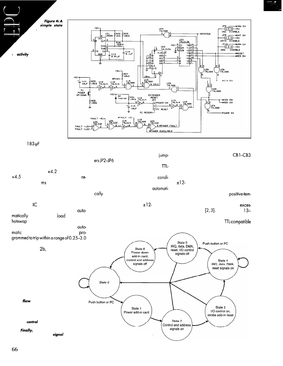
machine con-
nects or discon-
nects the logic and
power lines in a se-
quence that ensures that
the add-in card can restart
ifs
after
being replaced
on a fully operational com-
puter. A push-button switch,
overcurrent fault signals, and
PC-controlled signals are used
as inputs for the activation of
the control
logic.
These glitches can lead to
system failures such as data
corruption and logic lockups.
Figure 2a presents the
glitch caused on a PC’s +5-V
power line by the sudden
and direct addition of a rela-
tively power-hungry add-in
card. This add-in card acts as
a 1.6-A,
load, caus-
ing a transient inrush current that peaks at
In the extender card, the desired +5-V
In the extender card, Raychem’s
approximately 22 A! The corresponding
fault current is programmed through
PolySwitch self-resetting fuses
voltage glitch on the PC’s +5-V power bus
(see Table 1). Power on and off
protect the PC and the add-in card under
peaks at0.8 V, resulting in a transientdrop
are controlled through the /SHTDWN
test from shortcircuitsand otherovercurrent
of the power bus to
V. The minimum
compatible input of the UCC3912.
fault conditions on these power buses. A
V required for normal operation
Overcurrent or thermal shutdown
small, four-pole relay connects the PC’s
stores only 0.5
later. This obviously
tions issue the /FAULT signal and are used
and -5-V power lines to those of the
violates the operational limits established
by the extender’s control logic to
add-in card.
for TTL logic, and always caused the PC to
isolate the PC bus from the add-in
freeze, report BIOS errors, or reboot itself.
PolySwitch devices are
card.
A new by Unitrode, the UCC3912
perature-coefficient resistors that rapidly
PC add-in cards using
and -5-V
increase resistance in response to
integrated electronic circuit breaker,
power buses seldom demand more than
sivecurrent flow
Optoisolators U
limits the peak
current on
0.25 A from any single supply line. The
U 15 monitor changes in resistance of the
to a preprogrammed value. In
limited use of these power buses minimizes
addition, this IC implements a fully
PolySwitch devices to issue
the risk for glitch-induced faults due to hot
indications for overcurrent fault
circuit breaker that can be
swapping.
conditions. Just as with
A with transient output of up to 4 A. As
shown in Figure
using the UCC39 12 to
power the same add-in card as before, the
glitch amplitude is only 0.27 V, effectively
eliminating the possibility of causing an-
noying logic faults.
Unconditional power off
Figure 5: The sequential states of the
state machine control the power and
signal
between the add-in board and
the PC. In state 0, the extender keeps the PC
bus isolated from that of the add-in card
while waiting for an input from the push button or the PC.
Once an activation signal is received, states I-3 connect the
address,
(except for the reset signai), and power lines of
the bus. State 3 produces an artificial reset signal for the add-in
card.
state 4 fuiiy links the buses and makes the state machine
wait for a
deactivation
from either the push button, PC, or power fauit before
proceeding to
bus disconnection.
CIRCUIT CELLAR INK SEPTEMBER 1995
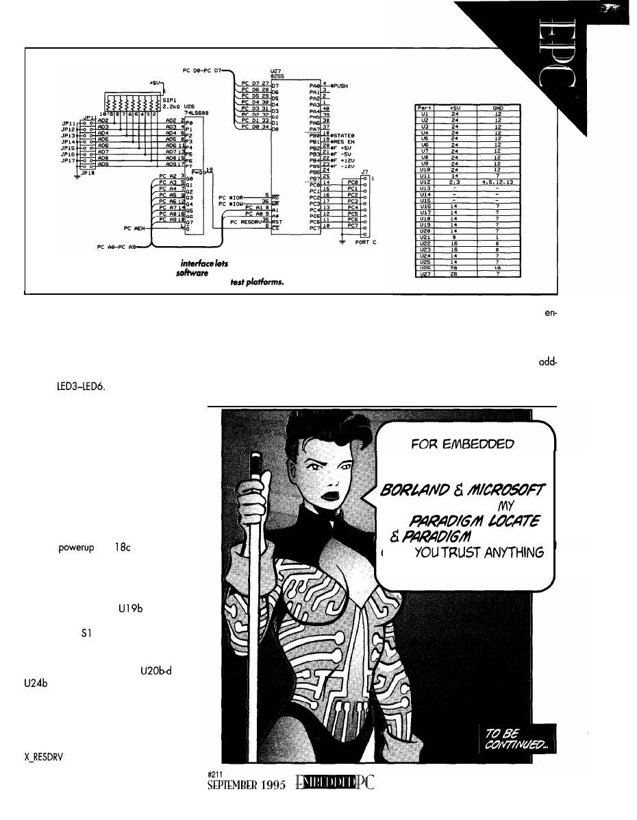
Figure 6: An 8255 parallel peripheral
sofhvare control the operation of the
extender card. An input port enables
to read the state and fault conditions of the
extender card, simplifying the design of automatic
overcurrent faults in the +5-V bus, these
cause the extender card’s control logic to
automatically isolate the PC bus from the
add-in card. latches U 16 and U 17 record
the tripping of overcurrent fault detectors
and visually indicate an error condition
through
CONTROLLING THE EXTENDER
The circuit of Figure 4 implements a
simple state machine to connect or discon-
nect the various logic and power lines of
the ISA bus in a sequence that ensures the
add-in card can restart its activity after
being replaced on a fully operational com-
puter. Synchronous counter U22 counts
pulses generated by U2 1, a 555 config-
ured as a
1 O-Hz clock. Depending on JP7,
the counter is unconditionally reset to zero
either at
by U
or by the PC’s
system reset line PC_RESDRV.
U23 decodes the S-bit count of U22 to
seven possible low-level true states. As
shown in Figure 5, when U22 is reset, state
0 causes the output of
to go high,
preventing U22 from counting. When push-
button switch is momentarily pressed,
however, U22 is enabled, allowing the
count to proceed.
As the count increases,
and
first enable connection of the power
lines on state 1. Then, on state 2, control
and address lines are connected, and in
state 3, the I/O control lines of the add-in
card are activated.
Additionally, state 3 strobes the
line through U 1 1 b, resetting the
add-in card. The strobe signal also resets
Pressing the push button again
any LED fault indicator tripped during the
ables the state machine to enter state 5,
previous cycle. When state 4 is reached,
where the lines activated by states 3 and 4
the PC reset, data, interrupt request, and
are deactivated. Finally, progressing to
DMA lines are connected to the add-in
state 6, U22 is reset to zero, and the
card. State 4 also freezes the count of U22,
in card is isolated from the PC expansion
allowing the card to operate normally.
bus.
C/C++ APPLICATION5
USING THE AWESOME
COMPILERS, I BET
LIFE
ON
DEBUG.
SAN
ELSE?
67
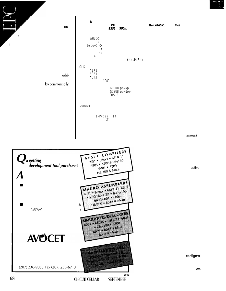
The rest of the logic
protects the PC from short
circuits in the add-in card
der test. Just after power is avail-
able to the add-in card, an overcurrent
f It
au on any of the power lines causes
the unconditional and asynchronous reset
of the counter.
TEST AUTOMATION
Powering the computer up and down
to reconfigure jumpers, make circuit
changes, and reposition probes may be a
tolerable annoyance when testing one
in card. But, as soon as you decide to try
your entrepreneurial skills
producing a batch of your own design,
testing and reworking with the least pos-
sible waste of time becomes a must. More-
over, you may want to automate the test
protocol so that a pass/fail evaluation of
your add-in cards can be carried out at the
assembly house in a time-efficient manner.
As shown in Figure 6, an 8255 PPI
enables software to control the operation
of the extender card. An input port lets
software read the state and fault conditions
of the extender, making it possible for you
Listing This sample program demonstrates confroiiing and inquiring the hot-swap
extender card from the
The program runs under
Notice
the default
base address for the
is
REM Control program for the hot-swap extender card
bas =
REM base address for the 8255
REM base port A
REM
port B
REM base+2 port C
REM base+3 control register
OUT bas 3, 128 + 8 + 2 + 1: REM PA output, PB and PC input
OUT bas. 1: REM set line 1
of port A to high
main:
Power UP add-in card"
Power DOWN add-in card"
Read current status of extender card"
PRINT: PRINT
EXIT": PRINT
INPUT menu
IF menu = 1 THEN
IF menu = 2 THEN
IF menu = 3 THEN
status
IF menu = 4 THEN END
GOT0 main
REM Power-up add-in card
REM First verify that card is not already powered up
status =
+
REM read status
IF (status AND = 0 THEN
PRINT "Add-in card already powered up": BEEP
FOR delay = 1 TO 4000: NEXT delay
RETURN
END IF
How do you know you’re
the most from your
Compare Avocet Systems
l
with the competition.
A Broad Line of High-Quality
Products at Competitive Prices
m Free On-Line Technical Support
for Registered
Users. No Voicemail!
Attractive Multi-User Discount Prices
Our
Educational Discount Plan
n
Unconditional 30-Day
Money-Back-Guarantee
to design an automatic test platform for
your product.
Strobing line 0 of port A has the same
effect as actuating the push button on the
extender card. The lines connected to port
B convey information regarding the
tion status of the extender card, as well as
of any overcurrent fault warnings that had
been issued. Port C is available through
connectorJ5, and you may use it as a logic
interface between your automated test pro-
gram and probes connected to the add-in
card under test.
listing
1
provides an example of how
to write your own extender card control
routine for an automated test program. The
program first configures the 8255 and sets
high line 0 of output port A. Activation or
Now call the obvious choice!
deactivation requests are handled by com-
paring the current state of the extender
card to the requested state, and issuing a
strobe on port A if necessary.
SYSTEMS; INC.
The Best Source for Quality
Embedded System Tools
( 8 0 0 ) 4 4 8 - 8 5 0 0
INSTALLING AND OPERATING
THE EXTENDER
Set the base address and
tion jumpers before inserting the extender
card into a free expansion bus slot in the
PC. An appropriate address for the
INK
1995
Listing continued
pushb: REM Strobe pushbutton signal
RETURN
REM Power-down add-in card
REM First verify that card is not already powered-down
status =
+
REM read status
IF (status AND = 0 THEN
"Add-in card already powered down": BEEP
FOR delay = 1 TO 4000: NEXT delay
RETURN
END IF
pushb: REM Strobe pushbutton signal
RETURN
status:
REM Read and display extender card status
CLS: PRINT "STATUS"
status =
+
REM read status
IF (status AND = 0 THEN PRINT "Add-in card powered down"
IF (status AND = 0 THEN PRINT "Add-in card powered up"
IF (status AND = 0 THEN PRINT "Fault on
line detected"
IF (status AND = 0 THEN PRINT "Fault on -5V line detected"
IF (status AND
= 0 THEN PRINT "Fault on
line detected"
IF (status AND
= 0 THEN PRINT "Fault on -12V line detected"
FOR delay = 1 TO 4000: NEXT delay
RETURN
pushb:
REM Strobe low push-button signal to toggle state of extender card
OUT bas, 0: REM Strobe push-button signal low
FOR delay = 1 TO 500: NEXT delay
OUT bas, 1: REM send signal back high
RETURN
You can verify that
.
the PC controls theextender
card by running the demon-
stration program. If conflicts with
other cards occur, change the base
address of
extender, modifying the
program accordingly. If all works well, you
may plug an add-in card on
while
1 and 2 are off, and then activate the
extender.
Once
1 and 2 turn on, simply run
the application software that uses the
in card, and proceed to probe the card.
Remember, however, that some add-in
cards (e.g., disk controllers, video adap-
tors, etc.) require initialization by the BIOS
after being reset.
To hot swap these cards, run a dedi-
cated program duplicating the BIOS initial-
ization of the add-in card under test. Only
then can you run the application software
that uses the add-in card. Alternatively,
configure JP7 to connect U
to the out-
put of U
and warm boot the PC each
time after activating the extender card.
Finally, always make sure you deacti-
vate the extender before removing or
reconfiguring an add-in card under test.
tender card PC interface can be selected
between 300h and 3 1 Fh, which is defined
by IBM as the location for prototype cir-
cuits. The example program assumes that
the extender card has a base address of
which is set with jumpers
JP15, while leaving
open.
Place jumpers on
and
to
enable connection and disconnection of all
bus lines to the add-in card. In addition,
configure jumpers
to program the
desired fault and inrush currents for the
V bus. JP7 selects the source for the uncon-
ditional reset of the extender.
Connecting
to the output of
U
resets the extender at
while
letting the add-in card remain connected to
the expansion bus during warm boots. In
the other position of JP7, the extender card
isolates the add-in card from the expansion
bus every time the PC issues a system reset.
Install the extender card, but don’t
insert an add-in card on connectors
yet. On
verify that
1 and 2
are off, indicating that the extender card is
inactive. Actuating the push button acti-
vates the extender
and
lights up
1 and
2. Pushing the switch once again deacti-
vates the extender.
Be a hero put Team Paradigm to work on your next
embedded x86 design and reap the rewards you deserve.
Team Paradigm has the ability to deliver all the embedded
system pieces from Intel to AMD, C/C++ or assembly
language, and all the Borland/Microsoft development tools.
Plus
Paradigm DEBUG
for your favorite in-circuit emulator
and real-time operating system.
So forget about making excuses and instead enlist
Team Paradigm for your current or next x86 project. We
deliver the finest embedded x86 development tools, backed
by unlimited free technical support. No one is more serious
about your success than Paradigm Systems. Call today
and get the details before you waste any more of your
precious time.
Proven Solutions for
Developers
I - 8 0 0 - 5 3 7 - 5 0 4 3
Paradigm Systems
3301 Country Club Road, Suite 2214,
NY
13760
748-5966
(607) 748-5968
Internet:
Paradigm Systems, Inc. All rights reserved.
IN CONCLUSION
Today’s PCs often come with a blend
of buses besides the basic
ISA bus.
The same principles described for hot swap-
ping on the ISA bus can be applied to hot
swapping on other buses. With additional
information on the signals, power, and
timing requirements of these standard buses
you can design a modified extender
card that lets you successfully hot swap any
add-in card.
In fact, you can even design an active
extender that enables you to use hardware
you could not normally interface to your
computer. By taking advantage of the
rent-limiting characteristics of the QS3384
it is possible to interface standard 5-V
logic to the new 3.3-V
logic used in
portable and “green” computers.
Despite the increasing popularity of
some of these new buses, ISA is alive and
well. Most add-in cards currently in the
market are compatible with either the 8-bit
or
ISA bus, and I dare to predict this
will not change soon.
Yes, do believe that eventually PCI or
some other enhanced bus will become the
interface of choice for desktop systems.
However, the considerable effort required
to design a fully compliant PCI interface in
Anatomyofa
Great Frame Grabber
Low Price
l
. ...*.
Precision
Small
l
Board
Half dot
Interface
C
source.
Call
800-366-9131
sampling
less than
V
I
n o i s e
Call and find out how
quality products, responsive technical
support and elegant software get
your application quickly to market.
Vision Requires Imagination’”
I-800-366-9131
l
Phone: 503-641-7408
l
Fox:
E-mail:
Homepage:
Box 276, Beoverton, OR 970750276
combination with the
lack of Plug-‘n’-Play hard-
ware and software standards
offer little hope of promptlygener-
alizing direct hot swapping on the
expansion bus.
Until then, I hope this extender card
eliminates the need for waiting-again
and again-for boot-up completion and
program initialization everytimeyou make
the slightest change to an add-in card
under test.
David
has
a Ph.D. in Biomedical
Engineering from Tel-Aviv University. He
is
an engineering specialist at Intermedics,
and his main R&D interest is biomedical
signal processing in
devices.
He maybe
imed.
corn.
REFERENCES
D. Strassberg, “Plug and Play,”
March 1995, 33-43.
T. Fang and S. Morris, “Conductive Polymers
Prolong Circuit life,” Design News,
Nov. 1992, 99-l 02.
J. Bachiochi, “Sacrifice for the Good of the
Circuit: Strengthening
the
Weak
link,” INK, 60,
July 1995, 82-85.
S.
“Understanding PC Buses,” INK,
50, Sept. 1994, 44-5
Quality Semiconductor, “Bus Switches Provide
to
logic Conversion with Zero
Delay,” Application Note AN-l 1, June 1993.
SOURCES
Integrated Circuits
7 Continental Blvd.
Merrimack, NH 03054
Quality Semiconductor
85 1 Martin Ave.
Santa Clara, CA 95050
Raychem Corporation
300 Constitution Dr.
Menlo Park, CA 94025
Active Extender card kit for
PC-ISA bus
[includes PC board and all
Active Extender card (assembled and tested
version).
A four-layer PCB [includes PC board and all
components).
Plus applicable taxes, postage, and handling.
Electronics
58 Chicory Ct.
Lake Jackson, TX 77566
4
19
Very Useful
420 Moderotely Useful
42
1
Useful
71
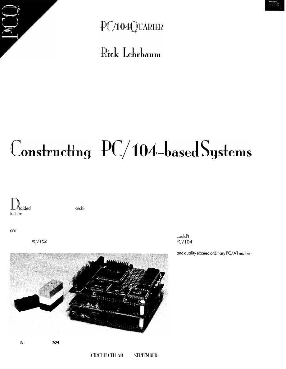
From plug-in memory cards for portables,
PCMCIA
has grown to include hard
disk drives, fax/modems, and other peripherals. Its use in the embedded
world is gaining popularity, especially with new
PC/7 04
offerings.
to use an embedded-PC
found CPU modules, display interfaces,
in that new development project?
data acquisition and control modules, and
Perhaps, it’s a portable data logger, a
other PC/l 04-related accessories and
vehicular performance monitoring system,
peripherals you can use to design and
telecommunications protocol converter.
build your system. No doubt, your supply
Maybe you’ve picked up your own
of PC/l 04 product information is steadily
copy of the
Resource Guide and
growing.
Photo Self-stacking PC/
modules are used
like embedded system building blocks.
72
INK
1995
So, when you selected your compo-
nents, did you choose PC/l 04 modules for
the embedded PC in your project because
they fit within a space where normal desk-
top motherboards and expansion cards
possibly go? Or, did you opt for
modules because their rugged-
ness, reliability, operating temperature,
boards, expansion cards, and peripher-
als?
Whatever the reason, you’ll likely dis-
cover that
by
using PC/l 04 modules, you’re
able to focus more on the specifics of your
application, especially the unique I/O,
packaging, and application software. You’ll
be through with wasting a lot of time and
money “reinventing the wheel.”
MACROCOMPONENT
BUILDING BLOCKS
You may have seen a picture like the
one in Photo 1, comparing
PC/l 04
mod-
ules to Lego building blocks. Although this
image points out how easy it is to build
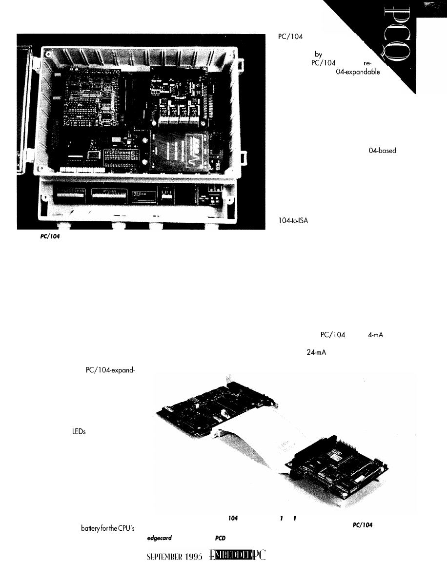
Photo 2:
modules can plug into application-specific baseboards like macrocomponents.
Application baseboards can contain data acquisition and control interfaces, keypad scanning
logic, power conditioning circuitry, and any other electronics needed by the application.
embedded systems with
PC/l 04
modules,
it’s wrong to conclude that every bit of the
electronics in your embedded system needs
to be on
PC/l 04
form-factor modules.
In fact, due to the specialized nature of
most embedded applications, systems of-
ten require unique functions or interfaces
not available in off-the-shelf
PC/l 04
mod-
ules. In short, be prepared to do some PC
board design in most cases.
Actually, the most common way to use
PC/l 04 modules is as macrocomponents
plugged into a custom,
able application baseboard. To meet spe-
cific application needs, the baseboard
contains various nonstandard functions.
As shown in Photo 2, the application base-
board could include signal-conditioning
logic, circuitry to scan switches or push
buttons, drivers for
or LCD displays,
DC power supplies or voltage converters,
and serial and parallel I/O ports.
The system in the photo monitors flow
rates in a gas pipeline. In this case, the
application baseboard includes two PC/
104 stack locations for a CPU and an
isolated digital I/O module. A hybrid
power-supply module, positioned directly
on the baseboard, powers the electronics.
Signal conditioning circuitry, real-world
connector interfaces, a
battery-backed clock, and miscellaneous
components are also included directly on
the baseboard.
Like most application baseboards, this
one adopts the shape of its enclosure. As
you can see, an application baseboard is
like a system motherboard. However, in-
stead of plugging I/O into a motherboard,
consisting mainly of a CPU, the CPU plugs
into a motherboard that consists mainly of
the application’s specialized I/O.
Besides providing efficient system logic
and interfaces not readily available on
modules, an
application baseboard can
reducecosts minimizing the
number of
modules
quired. Also, a PC/l
application baseboard that integrates
several required functions might be the
only practical way to fit everything needed
by your application into the space avail-
able.
IF YOU CAN’T BEAT ‘EM,
JOIN ‘EM
You can also expand PC/l
embedded systems with desktop PC expan-
sion cards. The easiest and least-expensive
way to accomplish this is with a passive
adapter cable. Such a simple interconnec-
tion is possible because the
PC/l 04
bus is
essentially
a
normal PC/AT bus-it just has
a different connector. Photo 3 shows a PC/
bus adapter cable.
Photo 4 presents a multislot PC/AT bus
backplane that takes this approach to the
extreme! Using this backplane, you can
combine a stack of PC/l 04 modules with
up to six PC/AT bus plug-in cards. A word
of caution: with such a setup, scope out bus
signals once you determine the system’s
final configuration. You need to ensure
over-and undershoot, ringing, andcrosstalk
are at acceptable levels. Also, be sure to
maintain control over what may be added
or altered in the future!
How can
with its
bus
drive mix with PC/AT bus plug-in cards
given the
drive of the PC/AT bus?
Even though this is true, the maximum load
Photo 3: The signals of the PC/
bus correspond -to- to the signals of the standard ISA bus
signals. As a result, a simple ribbon cable can be used to connect between a
CPU and
a standard ISA bus expansion card. To make this cable, you need to use a special, cable-mount
connector from
Connectors.
73
Photo 4: This ISA bus passive backplane from Douglas Electronics lets a
module stack
drive up to six standard or
ISA bus expansion cards.
of a normal PC/AT expansion card is
precisely the same as that of a
module: 0.4
For this reason, it theoreti-
cally makes no
whether
you add standard PC/AT bus cards or PC/
104 modules to a PC/l
system.
A T A L E O F T W O B U S E S
Another interesting alternative for ex-
panding PC/l
systems results from
teaming up PC/l 04 and PCMCIA. These
popular PC-related standards combine in a
highly synergistic way to meet the needs of
many types of embedded applications.
Table 1 compares some of the key
attributes of
and PCMCIA. PC/
104’s compactness (3.6” x 3.8” x
ruggedness, reliability, and inherent PC
compatibility enable it to provide the core
computer functions required by your em-
bedded-PC-based application. A small stack
of PC/l 04 modules typically
the
entire PC/AT motherboard logic (CPU,
BIOS, DRAM, system bus), serial and par-
allel ports, disk controllers, display control-
lers, and a
interface. Also, because
modules mount rigidly to each
other and other system components, the
system you build with them should with-
stand the shock and vibration requirements
of your application quite well.
Many of the characteristics that make
PCMCIA suitable to the mobile computing
also make it a good adjunct to PC/l 04 in
embedded applications. In particular,
74
PCMCIA’s small size, low power require-
ments, and
able. As well, PCMCIA cards are
especially appropriate to PC-compatible
hardware and software
after all, that’s what the “PC” in PCMCIA
is all about!
You might want to use PCMCIA
cards to expand PC/l 04-based systems
with the options popular for laptop com-
puters. The growing variety of PCMCIA
cards in this category include:
l
hard disks
l
flash and battery-backed SRAM cards
l
modems
l
LAN adapters
l
wireless communications inter-
faces
l
multimedia interfaces
l
GPS receivers
On the other hand, you’ll
find a better assortment of PC/
104 modules for functions and
interfaces specific to real-world
data acquisition and control ap
Some examples of
available PC/l 04 modules are:
l
analog and digital I/O
l
relay drivers
l
counter/timers
l
stepper and servomotor con-
trollers
l
touch interfaces
l
video frame grabbers
l
field buses: IEEE-488, Profibus, CAN,
MIL-STD-1553, ARINC-429, Echelon
LON
l
CRT and flat-panel display interfaces
l
digital signal processors
l
power-supply modules for industrial and
vehicular environments
S T A C K ‘ E M U P !
An important difference between PC/
104 modules and PCMCIA cards is how
they physically mount within the system.
modules stack rigidly with each
other (and other system components), mak-
ing them somewhat “permanent” system
components.
In contrast, PCMCIA cards are in-
tended to be used as removable devices.
This makes PCMCIA cards an ideal way to
provide removable, yet rugged, mass-stor-
age devices. When the system’s operating
software is located on a PCMCIA card, it’s
easy to reconfigure the operation of the
04 PCMCIA
Size (sq. in.)
13.7
7.2
Max. component
0.435
Type 1: 0.13
thickness (in.)
Type 2: 0.20
Type 3: 0.40
Power (typical)
0.1-0.3
PC compatible
yes
yes
Supports DOS drivers
yes
yes
Rugged, shock proof
yes
yes
Rigidly attached
yes
no
Operating temp.
Self stacking
yes
no
Readily removable
no
yes
Table 1: A comparison of PC/ 104 and PCMCIA
quickly points out how well they fit
in
embedded applications where space, power
consumption, and reliability ore important.
04 and
Normal
PCMCIA
PC/AT
Size (cubic in.)
50
1500
Weight (lb.)
1
40
Power
50-100 w
PC compatible
yes
yes
DOS/Windows compatible
yes
yes
Rugged, shock proof
yes
no
Operating temperature:
Standard
Extended
Expansion “slots”
2-3
04
ISA
l-2 PCMCIA
Removable storage
flash memory floppy disks
media
Table 2: Sometimes
ideal system involves a combi-
nation of
04 and
technology. The combina-
tion
all the punch-and
som-f a typical
PC/AT
at a fraction of the size, weight, and
power.
Photo 5: PCMCIA
be used like o miniature bockplone bus
in
opplicotions. This slot
PCMCIA
from
lets
combine one or two
PCMCIA
with o
system or update the software to fix bugs or
enhance features.
PCMCIA slots also let you add options
or upgrades in a
embed-
ded system. Over time, you can pretty
much count on the growing popularity of
PCMCIA in the laptop and other mobile
computing mass markets to spawn an in-
creasing variety of PCMCIA modules.
LIKE A TINY BACKPLANE
Photo 5 shows a two-slot PCMCIA
interface combined with a PC/l 04
board PC/AT computer. This stack can be
expanded two ways:
l
by stacking one or more PC/l 04 mod-
ules on a CPU module
l
by inserting one or two PCMCIA cards in
the two-slot PCMCIA interface.
You could
of this hybrid system’s
slot PCMCIA interface as a tiny backplane
supplementing
PC/l 04’s
stackability.
In a sense, the PC/l 04 module stack
shown in Photo is a lot like a “normal”
PC/AT system. Typically, a PC/AT system
consists of a CPU, RAM, and several ISA
expansion slots on a motherboard,
storage interfaces, and a display control-
ler. To configure the system for
a
specialized
application, insert various ISA expansion
cards in the five or six spare slots on the
motherboard.
As Table 2 indicates, the equivalent
PC/l 04 and PCMCIA system contains the
same functions, provides simi-
lar expandability, occupies
the
volume, consumes less than
the power, and weighs
as much!
ROLLING YOUR OWN
If
you need custom expan-
sion modules, you’ll quickly
discover that PC/l 04 is a bet-
ter choice than PCMCIA. PC/
104 provides a standardized,
easy-to-implement form factor
to facilitate design.
Although PC/l 04’s hori-
zontal and vertical dimensions
are strictly defined by the
module’s
in most cases
you won’t have a hard time
meeting its requirements using
normal components and a bit
of care.
CONCLUSION
Unlike ordinary bus
standards,
offers a
greater degree of flexibility and
does not restrict you to a typical
“stack and rack” mentality. To fully ap-
.
preciate the wide variety of ways you can
use
modules, think of them as
macrocomponents, which can be used both
as plug-in components and self-stacking
building blocks.
.
Other popular PC-oriented standards
such
OS
PCMCIA combined with PC/l 04
help you achieve even greater flexibility
and functionality.
Rick lehrbaum
Comput-
ers where he served as vice president of
engineering from
to 199 Now, in
addition to his duties as Ampro’spresident,
Rick chairs the PC/
Consortium. lie
On the other hand, squeezing your
bright idea into a custom PCMCIA card is
a daunting task. It is likely to be a difficult
and costly process because of PCMCIA’s
severe restrictions on component thickness
and other packaging requirements.
I R S
422
Very Useful
423 Moderately Useful
424 Not Useful
HOT
ELECTRONIC EXTENDERS
Insert/Remove Cards w/the PC Power On!
Save Time Testing and Developing Cards
Save Wear on Your PC from Rebooting
Adjustable Overcurrent Sensing Circuitry
ISA
Mini Extender
NO Fuses, All Electronic for Reliability
Classic Extenders with All Lines
Clearly Marked for Convenience
q
Save Time Testing, Developing, and
Repairing Computer Adapter Cards
Available Optional Tes Pin Headers
Under Top Connector
1
Year Warranty and 30
Day Money Back Guarantee
3343
D VINCENT RD
PLEASANT HILL, CA 94523 USA
800-209-2418
FAX 510-947-1900
Call our 24 Hour Fax-On-Demand System for FREE Information.
75

m
PCs
and How?
you
embedded
PCs,
you’ve got
start at
outlining
basics and making sure everyone is speaking the
same language.
Subsequent columns will delve into the nitty gritty of embedding a PC.
o doubt, you’ve been using embed-
ded microcontrollers and PCs for years,
although for totally different tasks. While
the idea of getting your personal computer
inside an embedded design sounds a little
far-fetched, recent technological break-
throughs have made PCs almost common-
place in the embedded world.
With the miniature, low-power, flex-
ible embedded PCs now
available,
a seem-
ingly unlimited number of applications
benefit from the use of embedded PCs.
And, there are many compelling rea-
sons
why
you
might wont to use an embed-
ded PC over either a non-PC-based
computer, a desktop PC, or an embedded
microcontroller.
That’s what this column is all about:
applying these powerful, flexible, fast-to
market, easy-to-program, convenient-to-in-
terface solutions to your new designs. I
plan to explore a wide range of topics
related to selecting, specifying, and apply-
ing embedded PCs. present and con-
trast alternative solutions, discuss some of
the not-so-evident aspects, point out prod-
ucts available in the marketplace, and
attempt to bring it all to life with real
examples. But, before I get carried away,
I want to make sure we’re all on the same
wavelength.
This month, after defining a few terms,
I’ll take a look at exactly what embedded
PCs are, who uses them, where, why,
when, and how. Following this, give you
a sneak preview of what’s coming in future
columns.
E M B E D D E D P C s D E F I N E D
Embedded PCs represent a powerful
and fast-growing subset of what is more
generally known as embedded systems,
embedded computers, or embedded con-
trollers. These terms each imply something
slightly
different, and you should be aware
of the distinctions between them before you
can appreciate how embedded PCs fit into
the picture.
An embedded system typically de-
scribes a device which packages computer
embedded systems is the user’s lack of
awareness about the presence of the com-
puter. To the user, the application is what’s
important, not that a computer implements
the solution.
Embedded computer and embedded
is incorporated into the solution or device.
microcomputerand microcontroller,
t h e d i s t i n c t i o n b e t w e e n t h e m s t e m s f r o m t h e
computer is typically used when a
not possess adequate performance
capabilities.
So, what then is an embedded PC? It’s
an embedded computer which possesses
most of the attributes of a personal
7 6
INK
1995
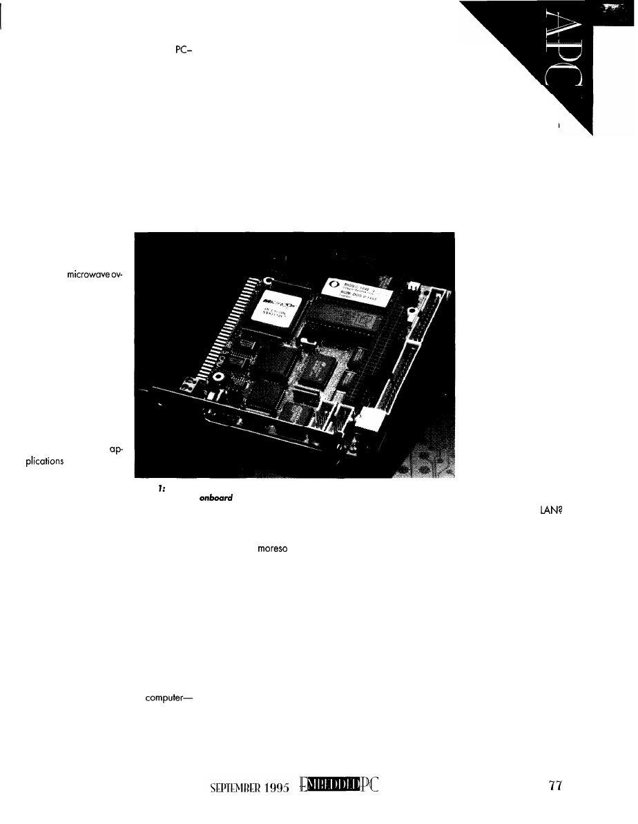
puter. Though not restricted to IBM
compatible systems, these systems repre-
sent the largest percentage of embedded
PCs available today.
What characterizes embedded sys-
tems is not the type of computer used, but
the computer’s relation to the application it
is used in. Typically, the computer is buried
in another device or system and, while it is
typically the critical component of the sys-
tem, the user is oblivious to the specific
computer chosen.
conveniently pipes into a spreadsheet pro-
gram for reporting results on a conven-
tional laser printer. Few would suspect,
however, that inside, at a detailed techni-
cal level, the device was very much like
their familiar desktop PC.
These days, embedded systems in-
volve a wide range of computers. At one
end are applications
which embed microcon-
trollers into everyday ap-
pliances like sewing
machines,
ens, automatic lawn sprin-
klers, and TVs. At the
other end are very pow-
erful, special-purpose
supercomputers embed-
ded in specialized equip-
ment which perform, for
example, a dedicated
portion of a complex
spacecraft navigation or
control mission.
While embedded systems are charac-
terized more by the application than the
computer, the computer acts as the heart of
the entire system. To the system designer
and implementer, the computer is the focus
of attention. However, since the computer
is often buried among sensors, actuators,
user interfaces, and other I/O devices
high-level language
tools. However, the ques-
tion of whether or not a VGA
display is the appropriate user
interface should receive proper at-
tention during
the
system design phase.
It should not simply appear in the system
by default.
But, these scenarios
represent the extremes.
Neither category of
would gener-
ally benefit from the use
of an embedded PC.
So, what kinds of
applications do embed-
ded PCs suit? How do we
This default response often occurs with
peripherals such as mice, too. While a
mouse is a convenient and useful for a
desktop computer, it often is cumbersome
and slow for an embedded system! Though
more difficult to interface and support in
software, another sort of
custom I/O capability
might be more conve-
nient for the user.
However, the wider
range of I/O devices
available for the PC
means that creative and
novel solutions benefit
from the presence of a
PC. For example, if an
application could benefit
from limited speech rec-
ognition, all thedesigner
needs to do is specify a
ready-to-go, off-the-shelf
board, which usually
comescompletewith driv-
ers and support software.
And if you need to
network multiple embed-
ded systems, what could
be more convenient than
a conventional PC
All the parts are there (at
cost), fully proven, sup
Photo Octagon‘s 40 IO Micro PC board plugs into conventional ISA slots or operates
standalone with
‘486 CPU as well as serial and parallel ports, floppy disk
controllers, and memory.
amazingly low
recognize them? What factors favor an
embedded PC over an alternative ap-
proach? While the detailed answer to
these questions will unfold in future articles,
let me identify some generic answers here.
W H O
An embedded PC is perceived quite
differently from the point of view of the
designer versus that of the end user.
Users are often completely unaware
of the computer’s presence. To be sure,
each user has an opinion about the system,
but none really cares that a
often an embedded PC-runs the inside
show.
However, if the users have computer
savvy, they might recognize the familiar
Windows GUI or appreciate that data
specific to the application, it must be treated
as a system
than just a computer.
One of the goals of designers and
engineers is often to hide the computer
from the user. This goal does not stem from
a desire for secrecy, but because users
should get to deal with on instrument on
their own terms. The computer should aid
and not interfere with the task at hand. This
is a particular challenge with embedded
PCs since a PC-especially from a soft-
ware perspective-comes with a beguiling
collection of familiar tools which the
implementer often uses for shortcuts.
For example, using a conventional
VGA monitor for the user console is tempt-
ing because it is already fully integrated
into the system and fully supported by
interface hardware, device drivers, and
ported, and ready to drop in. Even wireless
links are available.
But the trick, once again, is to blend
readily available resources into an appro-
priate system through a judicious mix of
hardware and software. Extreme care and
caution must be taken to avoid the tempta-
tion of forcing inappropriate restrictions on
the end user for the sake of implementation
expedience!
W H A T
So what characterizes an embedded
PC? What makes it the best choice in some
instances rather than an embedded com-
puter or controller?
Contrary to popular opinion, proces-
sor speed is not usually the overriding
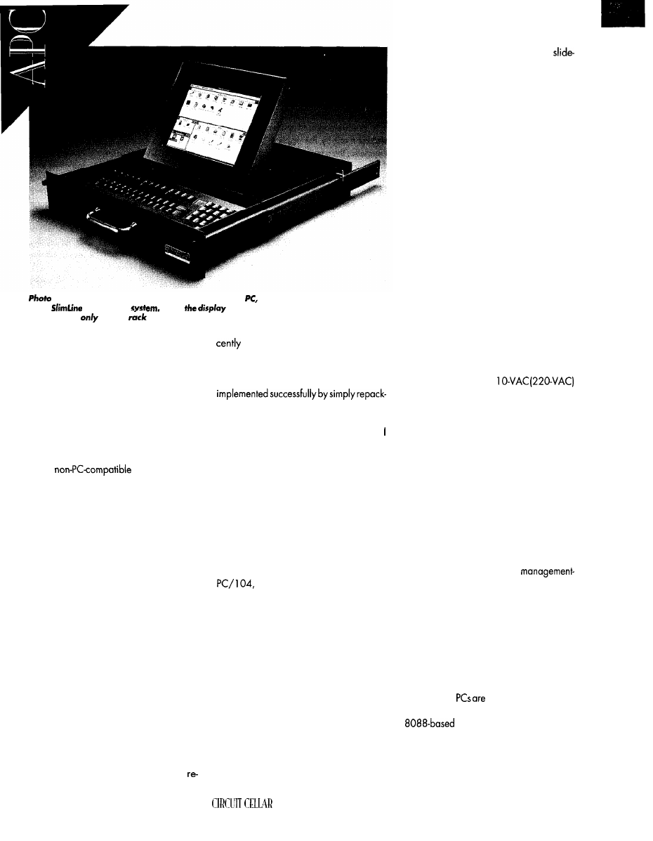
2: Interactive Display Systems packages a complete
keyboard,
and color LCD dispiay
in its
rack-mount
When
is folded down into storage position, the
unit occupies
3.5” of
space.
determining criterion. More often, a
microcontroller lacks powerful mathemati-
cal capability, memory addressing capa-
bility, or off-the-shelf peripheral interfaces.
Certainly, you could add floating-point
math, banked-memory controllers, and dis-
play and disk controllers to a microcontrol-
ler. But, this is time consuming from both a
hardware and software development point
of view.
A
microcomputer
might offer the processing power needed,
but it often comes up short on available
peripheral interfaces and software support
tools. Also, learning the peculiarities of a
new microcomputer is time consuming and
expensive.
An embedded PC is the best choice
when a number of its attributes suit the
application at hand. One would rarely use
an embedded PC in the design of elec-
tronic controls for a microwave oven or an
automatic lawn sprinkler system. Any num-
ber of embedded controllers represent a
less costly, simpler, and completely ad-
equate solution.
On the other hand, many other appli-
cations (e.g., medical instruments, data
acquisition and processing systems, ve-
hicular controls, operator displays and
user interfaces, advanced position-control
systems, automatic teller machines, auto
mated toll booths, video and other games,
and so on) beg for many of the features of
a common PC. The obstacle until just
78
has been the PC’s size, packaging,
high power consumption, and lack of rug-
gedness.
A few applications can actually be
aging a conventional desktop PC
motherboard with its ISA, EISA, VESA, and
PCI slots and peripheral interface cards.
supervised the implementation of an auto-
mated teller machine that successfully used
this approach in a design intended for the
benign environment of a bank lobby.
However, the poor mechanical stabil-
ity, connector reliability, and heat flow
associated with conventional PC mother-
boards would make this approach totally
unsuitable in a harsh environment.
Here’s where a wide variety of em-
bedded PC formats shine. VME, STD bus,
I-Pack, SBX, and proprietary
single-board solutions all strive for higher
reliability in a more suitable form factor.
Octagon’s Micro PC form factor shown in
Photo 1 illustrates the combination of con-
ventional PC ISA bus, PC/l 04 expansion
slots, and dedicated peripheral controllers
all on one board.
Some novel packaging approaches
exist too. You can use a flat-panel display
with an entire computer housed inside. Or,
when I/O requirements are minimal, con-
sider a “computer within a keyboard”
solution, complete with IAN capabilities.
For space-orsecurityconscious rack-mount
applications, interactive Display Systems
INK SEPTEMBER 1995
offers a system with pop-up display,
out keyboard, trackball, power supply,
and full-capacityembedded PC all in a unit
that slides into 3.5” rack height (Photo 2).
Regardless of which form factor you
select, you’ll find yourself in familiar terri-
tory when you boot the system and see the
familiar BIOS and operating system signs
(unlessyou’vesuppressed them). The board,
stack, or box you select to meet your
environmental and packaging needs will
undoubtedly be more rugged and reliable
than the PC on your desk. While it prob-
ably won’t resemble it, it sure as heck
operates like it!
W H E R E
Where does one use embedded PCs?
l
where the environment is more restrictive
l
where the system might be exposed to
physical extremes of temperature, shock,
vibration, or humidity
l
where space is at a premium or mounting
constraints are awkward
l
where power is available from other than
a steady, clean 1
wall outlet
l
where available power is minimal
l
where the system must put itself to sleep
for extended periods and then wake up
to perform a task autonomously without
human intervention
In other words, embedded PCs work in
potentially every application outside of a
home and office setting!
Embedded PCs are also ideal when
the embedded system must communicate
with other systems. For example, through
IAN support, factorycontrol systems link
data-acquisition systems and
reporting systems or facilitate the transfer
of remotely collected data back to the
laboratory where it is further processed by
conventional PCs. The commonality of disk
and data formats between the remote and
local systems is a real convenience and
time saver.
They are also ideal where it is desir-
able to offer a range of processing capa-
bilities. Since
in manywayssoftware
compatible with everything from a lowly
unit to thelatest Pentium chip,
it is simple to configure an assortment of
systems with a spectrum of capabilities
(and prices) while retaining the same core
software.
This flexibility lets users keep costs low
to meet current needs, while retaining the
option of upgrading in a modular fashion
to a more advanced system in the future
without completely scrapping earlier in-
vestment. It also provides a path of growth
to incorporate new, still nonexistent tech-
nologies into an embedded system.
WHY
Why use embedded PCs? Well, be-
cause they
l
pack a lot of processing power in a small
space
l
operate from low power
l
come fully equipped with BIOS and OS
support
l
are familiar and friendly to use
l
support high-level languages and debug-
ging tools
l
come packaged in a wide variety of
formats
l
are supported by a wide range of periph-
eral interfaces
l
are more rugged and reliable than desk-
top computers
l
run a plethora of off-the-shelf software
l
provide a softwarecompatible range of
processing capabilities
l
offer a migration path for the future
l
are familiar to a large number of design
engineers, programmers, and product
users
Need I say more?
W H E N
When is an embedded PC the best
choice? I’ve touched on a few physical
factors like ruggedness, reliability, immu-
nity to high (or low) temperatures and high
humidity, and compact size. But, there are
other, more subtle factors that often bend
the decision in favor of an embedded PC
approach.
Embedded PCs improve time to mar-
ket, especially when development resources
are scarce. There are probably more de-
sign engineers and programmers familiar
with the PC than any other single-computer
platform. The learning curve is much less
than for any other solution.
These advantages are not without risk,
however. Would-be embedded-system
implementers often have no knowledge of
or experience with time-critical, real-time
embedded systems. Many have completely
HUGE BUFFER
FAST SAMPLING
SCOPE AND LOGIC ANALYZER
C LIBRARY W/SOURCE AVAILABLE
POWERFUL FRONT PANEL SOFTWARE
$1799 DSO-28204 (4K)
$2285 DSO-28264 (64K)
DSO Channels
2 Ch. up to 100
1 Ch. at
4K
or
64K
Cross Trigger with LA
125 MHz Bandwidth
Logic Analyzer Channels
8 Ch. up to 100 MHz
4K or 64K
Cross Trigger with DSO
Free
software updates on BBS
Powerful
menu driven software
up
to 128 Channels
up to 400
MHz
up
to
16K
Samples/Channel
Variable Threshold Levels
8 External Clocks
16 Level Triggering
Pattern Generator Option
LA12100 (100 MHz, 24
C h )
LA32200 (200 MHz, 32
C h )
LA32400 (400 MHz, 32
C h )
LA64400 (400 MHz, 64
C h )
Call (201) 808-8990
Link Instruments
369
Passaic Ave, Suite 100, Fairfield,
NJ 07004
fax:
808-8786
1995
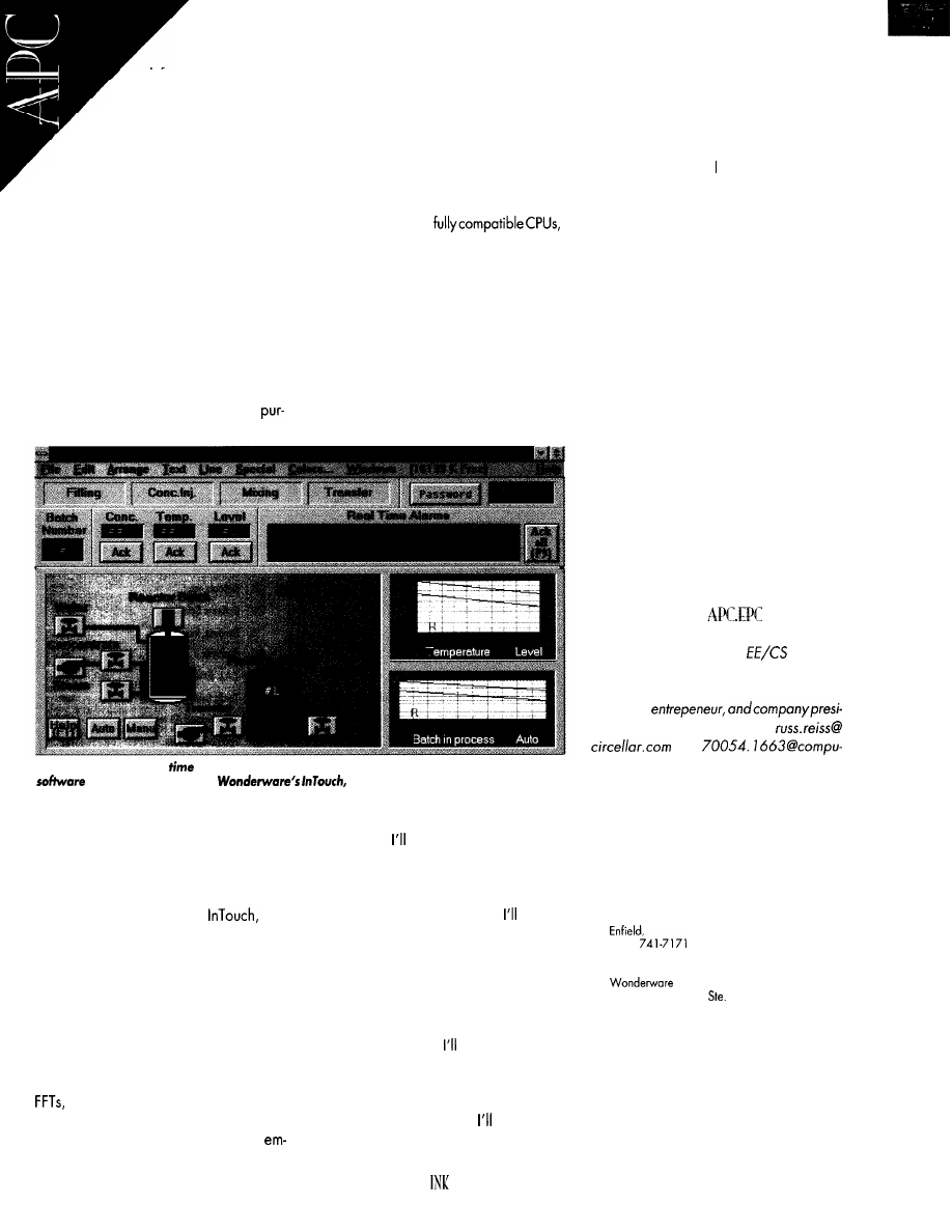
left the “details” of I/O
up to an operating system
that not only may be found
lacking, but may get in the way.
My point: implementing most
embedded systems is quite different
than implementing a payroll or billing
system. You still need an embedded-system
engineer, not just a PC programmer to pull
off most successful designs.
The embedded-system engineer has
available a plethora of tools-especially in
software-which are widely accessible,
less costly, and more user friendly and
familiar than tools for competing systems.
And, I’m not talking simply assemblers, C
compilers, and diagnostics.
In some cases, complete end-user soft-
ware already exists which can be
bedded PC while others carry over from the
desktop PC.
With embedded PCs piggybacking
the desktop PC marketplace, there is a
built-in guarantee of new and more power-
ful solutions arriving each day. An embed-
ded PC offers an unparalleled migration
path. One can be sure that tomorrow will
bring more powerful,
and an ever-growing choice in peripherals
and controllers with phenomenal perfor-
mance and lower cost.
and HOW...
How do you use embedded PCs?
That’s what this column is all about.
In coming EPC sections, I’ll look at
many important issues that arise when
applying embedded PCs. For example,
Photo 3: Considerable
and programming effort can be saved by using off-the-shelf PC
in embedded systems.
for instance, permits rapid implemen-
tation of operator control-panel displays in diverse applications.
chased at reasonable prices and handles
much or all of the system requirements.
Consider the proliferation of what might
generally be called operator console soft-
ware such as Wonderware’s
pic-
tured in Photo 3.
These programs can instantly trans-
form a conventional (or flat-panel) monitor
screen into a customdesigned front panel
for your new system complete with the
dials, gauges, bar graphs, annunciators,
and push buttons accessible to the user via
a convenient touch panel. There are also
full-blown programs for data-acquisition,
and displaying histograms and strip
charts on a screen or printer. Some soft-
ware is designed specifically for the
82
next quarter, present the various board
and bus configurations which are avail-
able and consider novel schemes for pack-
aging your nifty embedded PC.
In a following installment, look at
the issue of selecting, interfacing, and
programming displays for embedded sys-
tems. After all, it’s unlikely that you’ll want
(or be able) to stick that big fat VGA CRT
monitor into your next miniature, portable
thingamajig.
In later columns, study techniques
for powering embedded PCs with other
than conventional line-powered supplies,
and look into unique peripherals for em-
bedded PC applications. investigate
topics ranging from the familiar PCMCIA
CIRCUIT CELLAR
SEPTEMBER 1995
slots to specialized rugged hard drives,
flash-memory systems, and ROM-DOS to
exotic peripherals such as GPS navigation
satellite receivers.
Finally, real examples will illustrate
many of these issues. wrestled long to find
a suitable vehicle that could encompass
such a wide range of topics yet not be so
particular that it would become boring.
Finally, I realized that o long-standing pet
project of mine-the computerization of
my old RV-represents an ideal vehicle
(pun intended).
Computers in an RV can serve many
purposes: engine, battery, and lighting
monitoring; security; navigation; and mun-
dane needs like word processing and tele-
communications. Furthermore, an RV
possesses a number of attributes, including
limited space, high shock and vibration,
fluctuating and electrically noisy DC power,
and need for day/night operation, all
criteria that provide fertile ground for inves-
tigating the application of embedded PCs.
While it is unlikely that anyone will
want to precisely duplicate the examples
I’m presenting, I’m hopeful you will find
them novel, interesting, and instructive. I
trust the principles will carry over to your
own applications.
Russ Reiss holds a Ph.D. in
and has
been active in electronics for over
25 years
as industry consultant, designer, college
professor,
dent. He
may be reached at
o r
serve.com.
SOURCES
Octagon Systems
65
10 West 91 Ave.
Westminster, CO 80030
(303) 430-l 500
Fox: (303) 426-8 126
Interactive Display Systems
Division of General Digital Corp.
198 Freshwater Blvd.
CT 06082
(203)
Fax: (203) 741.7071
Software Development, Corp.
16 Technology Dr.,
154
Irvine, CA 92718
(714) 727.3200
Fox: (714) 727.3270
I R S
425
Very Useful
426
Moderately Useful
427 Not Useful
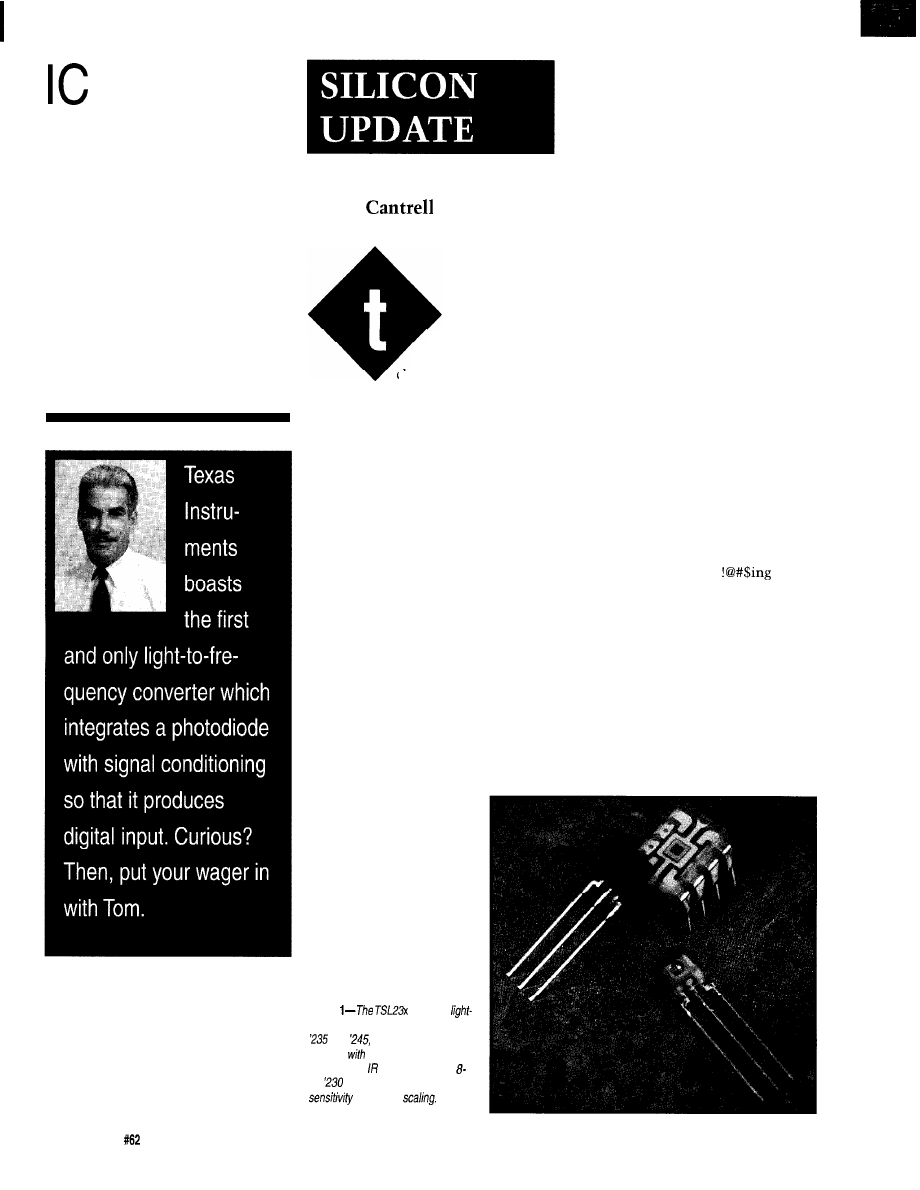
de Light
Tom
he kids are
parked in front of
the TV, so now’s my
chance to sit down in
front of the old Mac and get to work
on my next INK article.
Sure enough, I don’t even make it
past the happy Mac face before the
mild-mannered morning takes a bad
turn. A large crashing sound is accom-
panied by what sounds like a primal
scream in a group-therapy session.
Storming into the living room,
I
stumble into a combat zone including
martial arts (accompanied by the
requisite battle cries), sword play
(never considered a mop a lethal
weapon until now), and lobbing of
Lego hand grenades.
What’s this? I’m sure I left the TV
on PBS. Where’s the purple dinosaur or
the old guy who wears the sweaters?
Instead, the kids are getting
inspired by the Mighty Barphin Dour
Strangers, who deserve nothing better
than a mighty big shot of morphine
Photo
series of
fo-frequency converters includes the
and
which are three-lead
devices,
the ‘245 (dark package)
optimized for applications. The
pin
features programmable
and output
(somewhere between coma and lethal)
as far as I’m concerned.
As I write this, debate once again
rages on the influence of TV on kids.
One side claims it’s much ado about
nothing while the other blames it for
most societal ills.
Me, I come down squarely in the
middle. First of all, anyone who
imagines violent TV doesn’t affect kids
either doesn’t have kids or never sees
them. On the other hand, I suspect
letting politicians choose what we
view is rather an iffy proposition.
I believe in censorship, as long as
it’s Big Daddy and Mommy, rather
than Big Brother at the controls.
Unfortunately, Big Daddy or Mommy
often have other Big Stuff to do.
So, I’ve pondered the problem of
how to control the kids’ viewing
habits without being chained to the
remote. Dismissing the obvious
(shotgun the TV) or infeasible (teach
kids to be respectful and obedient)
leaves technology as the only hope.
Cable boxes have a channel
lockout feature. VCRs can be pro-
grammed (where is that
manual?) to turn on and off and record
a particular channel. So, I imagine it’s
only a matter of time before some
clever TV engineer (likely one with
kids) comes up with the bright idea of
making a kid-proof TV (i.e., one which
can lock out certain channels at
certain times). Editor’s note: This
feature already exists for high-end
TVs. Sanitizing the TV would take a
trivial amount of extra logic (if any)
84
issue
September 1995
Circuit Cellar INK
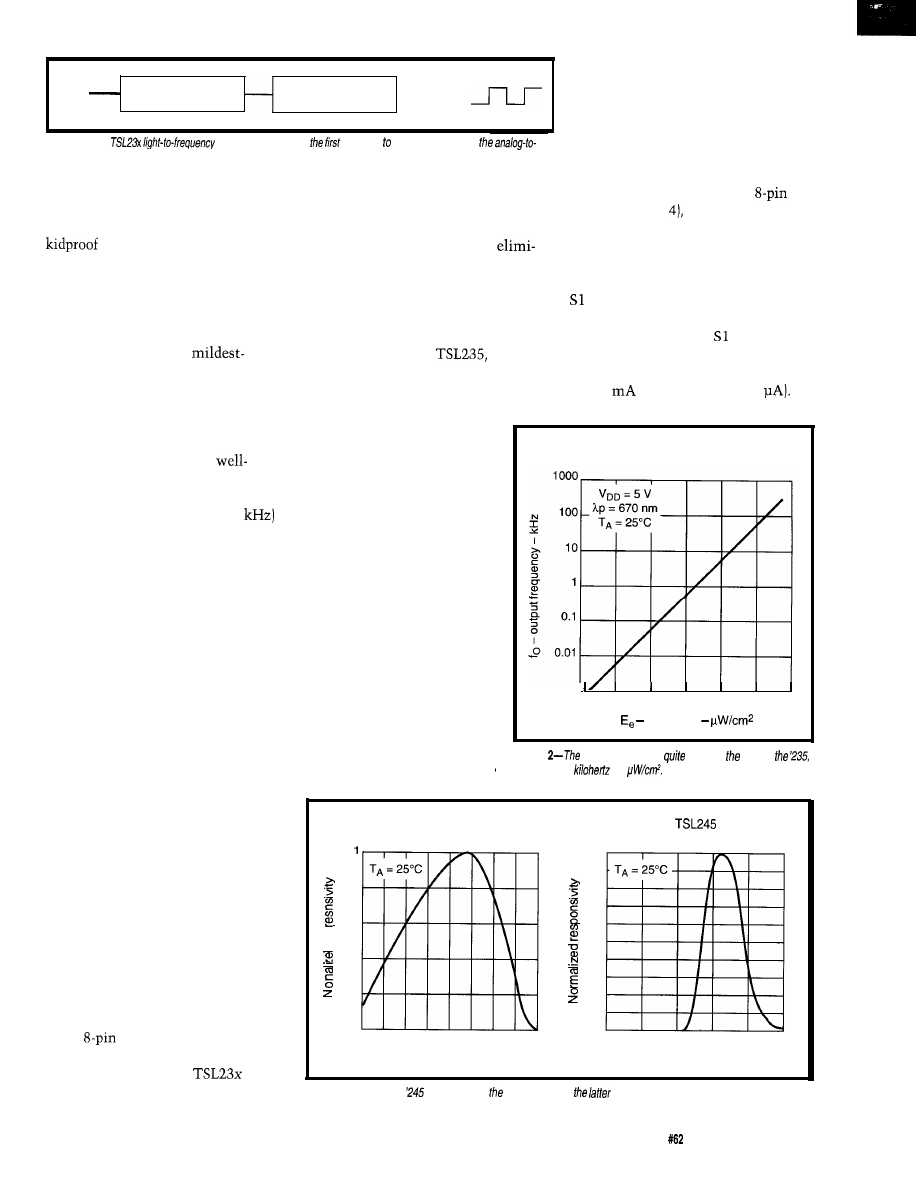
Light
Photodiode
Current-to-frequency _
converter
o u t p u t
Figure l--The
devices are among
sensors completely bridge
digital gap.
since modern units already have a
CPU and EEPROM.
However, the emergence of
TV sets won’t help the
millions with the older models. So, my
bright idea is to make a little box
(safely mounted high on the wall) with
a micro, real-time clock, and IR LED
that acts as a censorial Cyclops by
prudently selecting the
mannered program every half-hour.
Diving right into the design, the
first step is to come up with a way to
learn the channel-select codes for my
particular TV. Fortunately, the subject
of IR and remotes has been
covered in previous
INK
articles,
explaining a variety of arcane formats
and modulation (typically at 40
schemes.
However, we really don’t have to
understand the details to get the
desired result. Instead, it’s quite
adequate to simply train the gadget to
mimic the TV remote [i.e., capture
what the remote outputs to select a
channel and, without the need for any
interpretation, play it back).
Thus, like a learning remote, my
cyborg censor can work with any and
all TVs.
A BIT OF LIGHT
In the old days, I’d collect a
handful of components including a
photodiode, op-amps, and their
requisite resistors and capacitors, and
have a go at it. Actually, I’d probably
give Steve Ciarcia or someone equally
blessed with analog know-how a call
and beg for help.
But, as of a couple of years ago,
things got a lot easier. Refer back to
“Op-amp Terminators”
(INK 43).
There, I described the Burr-Brown
OPT201, a device integrating all the
aforementioned components in a
single
DIP which easily con-
nected to an A/D converter.
Now, thanks to the
series
of intelligent optosensors from Texas
covers the UV and visible spectrum
while the ‘245, thanks to its dark
package, is optimized for IR response.
The latter sounds like just the ticket
for any gadget that wants to work with
the worlds ever-growing collection of
remotes.
Instruments, the task of turning light
to bits is even easier. Following the
“Go digital, young man” catch phase,
TI ups the integration ante by
The ‘230, packaged in an
DIP (see Figure features the same
spectral (UV to visible) response as the
‘235. The extra pins hook to additional
nating the need for an expensive A/D
converter port. Indeed, TI claims their
light sensor is the first to totally bridge
the analog-to-digital gap.
The offerings pictured in Photo 1
include the TSL230,
and
TSL245 and are based on a common
architecture. As you can see in Figure
1, the chips convert light
input to a digital frequency
output. At only $1.75 for the
‘235 or ‘245 (in 1000s) and
about a buck more for the
‘230, a ride on the digital
bandwagon isn’t going to
empty your wallet.
features including programmable
sensitivity and output scaling. SO and
can select three levels of sensitiv-
ity:
1,
10, and 100 times. The fourth
combination of SO and (both low)
puts the ‘230 into low-power mode,
which cuts power consumption from
low (3
active) to trivial (10
Output frequency vs. irradiance
The ‘235 and ‘245 are
packaged in three-lead
packages, which include
power (2.7-6 V), ground, and
output. The latter is a square
wave whose frequency
corresponds quite linearly to
the light intensity, as shown
in Figure 2.
The main difference
between the devices is the
photodiode spectral response,
as shown in Figure 3. The ‘235
0.001
0.001
0.01
0.1 1
10 100
l k
irradiance
Figure
device’s
output is
linear. In case of
if’s roughly a
per
TSL235
photodiode spectral responsivity
photodiode spectral responsivity
1
0.9
0.6
0.6
0.7
0.6
0.6
0.5
0.4
0.4
0.2
0.3
0.2
0.1
0
0
300 400 500 600 700 800 900 10001100
600
700
600
900
1000
1100
hinnm
hinnm
Figure
3-The ‘235 and
are essentially same, except
is optimized
for/R applications.
Circuit Cellar INK
Issue
September 1995
85
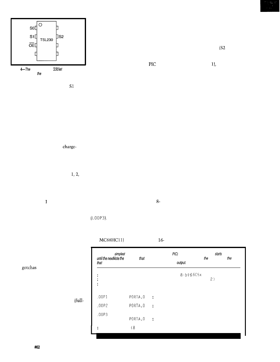
0
G N D
s 3
TSL230
O U T
vcc
Figure
extra pins of fhe
designers
dynamically adjust sensitivity and output-frequency
divide ratio.
You might suspect SO and
control (as in a discrete design) a
programmable gain amp. Actually, the
technique TI refers to as
electronic
aperture
is much simpler. It turns out
there are actually 100 closely matched
photodiodes (10 x 10 matrix) on the
chip. Selecting the sensitivity is
simply a matter of enabling either 1,
10,
or all 100 of them.
The photodiodes’ output is in turn
fed to a switched-capacitor
metering circuit (i.e., A/D converter
surrogate) that produces a frequency
output.
S2 and S3 set the scaling of the
frequency output as a divide by
10, or 100, allowing designers to
personally tune the tradeoff between
measurement speed and the timing
capabilities of the attached micro. All
but the divide-by-
or the low half can be measured.
F i n a l l y , t h e r e ’ s a n O E ( O u t p u t
E n a b l e ) p i n t h a t l e t s t h e ‘ 2 3 0 s h a r e a n
color applications.
WE INTERRUPT THIS PROGRAM
Taking a light reading is conceptu-
ally simple (i.e., just measure the
f r e q u e n c y o f t h e o u t p u t ) , b u t t h e r e a r e
some
to watch out for depend-
i n g o n y o u r a p p l i c a t i o n a n d t i m i n g
resources.
The speed with which a single
reading can be taken obviously de-
pends on the light level and can vary
from a second or so (dark) to 1 us
scale illumination). If the speed of
r e s p o n s e i s n ’ t c r i t i c a l , t h e u s u a l
oversampling and averaging tech-
n i q u e s c a n b e u s e d t o f i l t e r o u t r a n d o m
or periodic noise such as the 60 Hz
c o m m o n l y f o u n d i n A C l i g h t i n g .
Whether using a dedicated timer/
bit resolution. However, a possible
counter, a general-purpose input, or
an interrupt request, the general
t h e c o u n t e r / t i m e r ( t y p i c a l l y , 8 o r 1 6
principle is the same. You can either
bits) may overflow, limiting the range
measure how many pulses occur in a
of measurement. Fortunately, the
given time or measure the elapsed
f r e q u e n c y - s c a l i n g f e a t u r e
and S3)
time for a given number of pulses. In
can be exploited to constrain the ‘230
either case, it’s no real brain teaser, as
output and, along with sensitivity
shown by sample code for the
a d j u s t m e n t ( S O a n d S
maximize
(Listing 1).
dynamic range.
With a digital interface you may
wonder, as I did, why TI didn’t just
include a counter to take care of the
housekeeping. However, I realized that
the decision to do so is hampered by
the same concern that keeps analog
sensors from stampeding to digital
overnight.
KEEP IT CLEAN
Included with the literature was a
When faced with the proposal to
include an A/D converter, sensor folks
always come back with “how many
bits?” Though the concern won’t stop
the inexorable move to digital, it is
valid. For one customer, 8 bits of
resolution may be adequate, while
another might need I2 bits.
‘230 simulator that runs on PCs (both
DOS and Windows versions are on the
disk). Given the simplicity of the
device, it’s not surprising the simula-
tor is a snap to use. As shown in Photo
2, it’s easy to set up the ‘230 sensitiv-
ity and scale factors, define a light
source (wavelength and intensity), and
observe the resulting output.
For the ‘230, the analog to analog
question revolves around timing
resolution. In other words, the resolu-
tion of the ‘230 is infinite, subject to
the minor constraint that you have an
infinite-resolution timer handy. For
example, it turns out the previous PIC
routine achieves the equivalent of
bit resolution, limited by the speed of
the code that increments the count
About the time I was ready to grab
the soldering iron, I realized my TV
cop idea had a few flaws. Sure, I
considered the fact the kids would
manually change the channel, but
figured I could just repeatedly send the
programmed channel command every
30 seconds or so.
However, I suspect it wouldn’t
take more than a few nanoseconds for
the little conspirators to figure out all
they have to do is block the TV’s IR
window. A casual wipe down with a
PBJ sandwich would be all it takes to
jam (er, jelly?) the link.
The TI literature shows that parts
with dedicated timer/counters (ex-
amples they give include the TMS370
and
can achieve up to
Instead, I now rely on a neural
network. In other words, I’ve recently
had luck encouraging (OK, bribing) the
oldest kid with computer games
Listing l--The
possible code (in this case for a
simply finds an edge and then
counting
one. restriction
divide-by-l mode can’t be used since code relies on fact
divide-by-2 (or greater) modes generate a square-wave
period measurement routine for PIC
Assumes input signal is 50% duty cycle (divide by
Does not account for overflow
MOVLW
FFH
FF is hex for 255
MOVWF
PCNT
Initialize period counter
BTFSC
Check port
GOT0
LOOP1
Wait for low level
BTFSS
Check port
GOT0
LOOP2
Wait for high level
INCF
PCNT
Begin counting
BTFSC
Check port
GOT0
LOOP3
Count while high
Value in PCNT bit) represents period/Z
86
Issue
September 1995
Circuit
Cellar INK
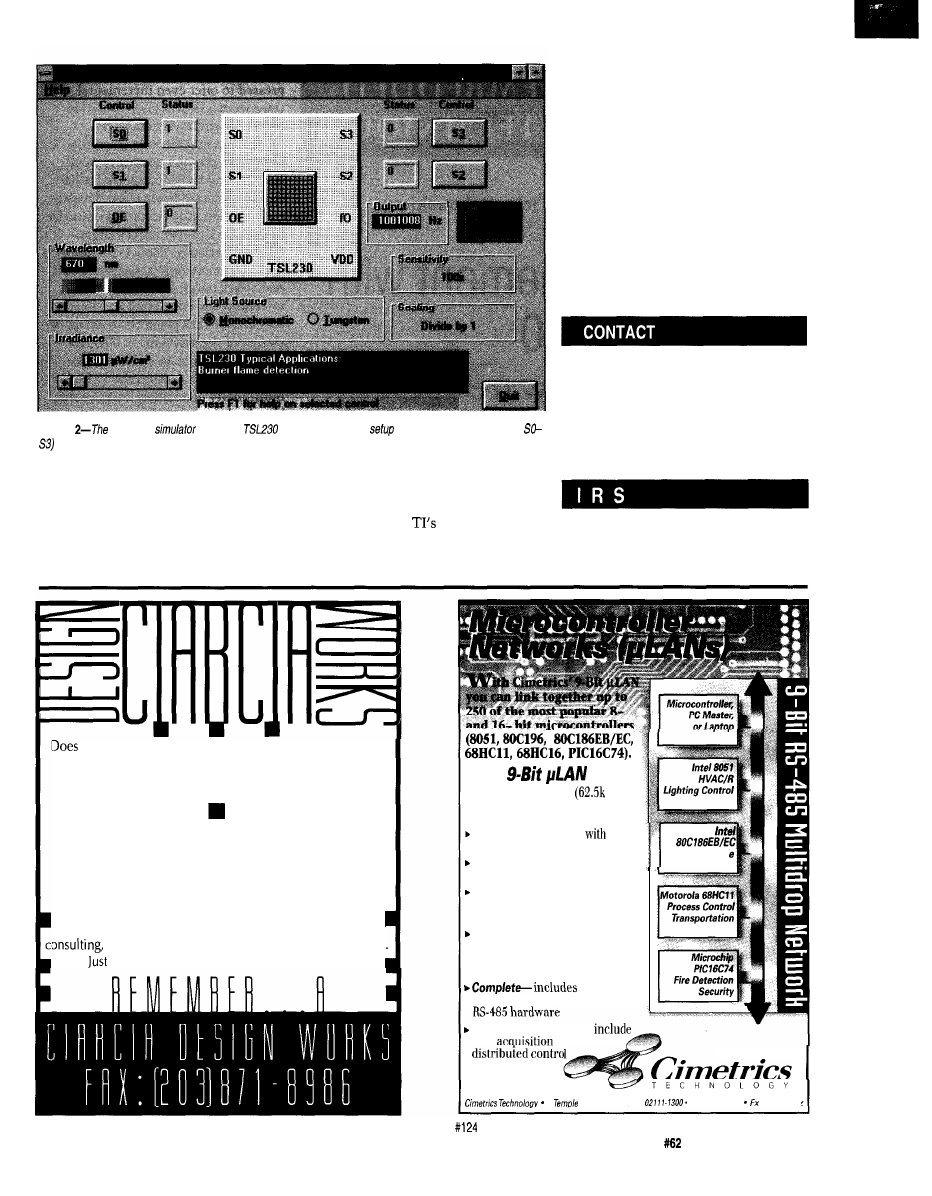
Photo
PC-based
shows the
output under various
(scaling and sensitivity inputs
and lighting (wavelength and intensify) conditions.
(educational, of course) to police the
Nevertheless, there are plenty of other
TV. Indeed, he’s become quite zealous
light-sensing applications that can
and can deal with the younger ones’
take advantage of
know-how.
plots or unexpected program schedule
Thanks to the ever-lower price of
changes far better than any CPU.
technology, you may find the chips
popping up in unexpected places-cars,
games, toys, cameras, and even your
dishwasher. In the latter application,
the ‘230 analyzes an illuminated water
sample to control the flow, tempera-
ture, and timing of the wash cycle.
q
Tom Cantrell has been working on
chip, board, and systems design and
marketing in Silicon Valley for more
than ten years. He may
be
reached
at
(510) 657-0264
or by fax at
(510) 657-
5441.
Texas Instruments, Inc.
Literature Research Center
P.O. Box 172228
Denver, CO 80217
(800) 477-8924, Ext. 3411
(303) 294-3747, Ext. 3411
428 Very Useful
429 Moderately Useful
430 Not Useful
your Big-Company marketing department come up with
more ideas than the engineering department can cope with?
Are you a small company that can’t afford a full-time
engineering staff for once-in-a-while designs?
Steve Ciarcia and the Ciarcia Design Works staff may have
the solution. We have a team of accomplished programmers
and engineers ready to design products or solve tricky
engineering problems.
n
Whether you need an on-line solution for a unique problem,
a product for a startup venture, or just experienced
the Ciarcia Design Works is ready to work with you.
fax me your problem and we’ll be in touch.
The
is:
. Fast-A high speed
baud)
multidrop master/slave RS-485
network
Flexible-compatible
your
microcontrollers
Reliable-robust IS-bit CRC and
Point-of-Sal
sequence number error checking
Efficient-low
m i c r o c o n t r o l l e r
resource requirements (uses
your chip’s built-in serial port)
Friendly-Simple to use C and
assembly language software
libraries, with demonstration
programs
network
Fire Detection
software, network monitor and
Practical-
applications
data
and
55
Place. Boston. MA
Ph 617.350.7550
617.350.7552
Circuit Cellar
INK
Issue
September 1995
87
John Dybowski
Power Management with
the
Part 2: The Software
0
ast
month’s
column focused on
the hardware aspects
of a general-purpose
computer with inherent soft power-
management capabilities. My discus-
sion centered around Dallas Semi-
conductor’s
and
processors.
Looking at modern power-manage-
ment techniques from the perspective
of a microprocessor shouldn’t be
surprising since this is the source of
most, if not all, dynamic signaling in
systems. In a CMOS system, remem-
ber any significant power consumption
results from dynamic dissipation. In a
properly implemented design, quies-
cent current flows at leakage levels
amounting to microamps.
If we agree that system-wide
power management is an extension of
power control at the processor level, it
should be apparent why I am so enthu-
siastic about Dallas’s accomplish-
ments. With the interest of keeping
power consumption in check, I find it
surprising that other controllers don’t
even come close in terms of power-
management capabilities.
A cursory survey of the competing
devices reveals that nothing significant
specifically deals with the power
issues plaguing many embedded
applications. Even some of the newest
embedded processors seem hard
pressed to offer even incremental
improvements over last-generation
power-control methodologies.
I suppose it all boils down to a
semiconductor manufacturer’s per-
spective and background. Dallas has
expended considerable effort develop-
ing and perfecting circuits specifically
targeted at administering
critical functions. Their expertise with
nonvolatile memories, nano-powered
real-time clocks, and a variety of
microprocessor and
sory circuits has given them an appre-
ciation of the problems of effective
embedded design on a global scale.
This experience culminates in the
multiplicity of ancillary features they
have built into their high-speed proces-
sor line.
Power management in embedded
systems is one of those things you
either absolutely need or just don’t
care about. To those experienced in
the field, the material I’m about to
present should uncover few surprises.
Those unfamiliar with the discipline
may gain new insight and develop an
appreciation for the realm where a few
microamps can spell the difference
between design success and market
failure.
In a fully CMOS system, power
management is synonymous with
clock management. What we are
trying to control is dynamic dissipa-
tion. Quiescent dissipation should
take care of itself as long as a few
basic guidelines are followed.
course, these criteria assume the
system is composed entirely of
micropower components. Obviously,
selecting the right peripherals can
make or break it.
The
supports the
traditional
1 Idle mode and Stop
mode. Additionally, you can select an
alternate clock source (e.g., a ring
oscillator) and invoke reduced
throughput modes such as
and
PMM2 (power management modes 1
and 2). Many features can be combined
to yield radical power savings at
degraded performance, moderate power
consumption with somewhat compro-
mised performance, or any nuance
between these extremes.
Issue
September 1995
Circuit Cellar INK
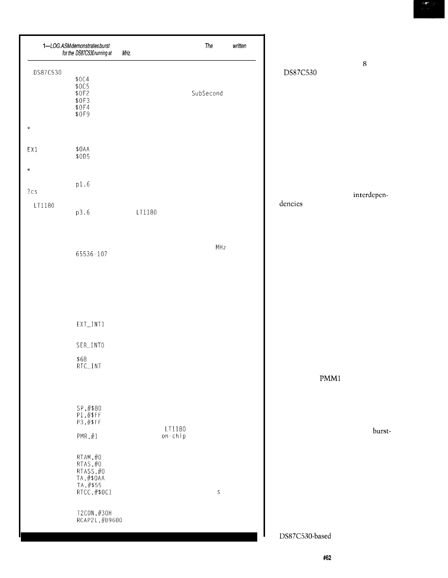
Listing
mode operation in a data logger device. code was
specifically
33
*
register equate table
PMR
EQU
Power Management Register
STATUS EQU
Status Register
RTASS
EQU
Real-time Alarm
Register
RTAS
EQU
Real-time Alarm Second Register
RTAM
EQU
Real-time Alarm Minute Register
RTCC
EQU
Real-time Clock Control
Bit equate table
RIO
BIT
898
Serial port 0 receiver int flag
TIO
BIT
$99
Serial port 0 transmitter int flag
BIT
External interrupt 1 enable bit
FO
BIT
General-purpose flag
LTC1392 I/O
?clk
BIT
p1.7
Clock bit
?dq
BIT
Bidirectional data
BIT
P1.5
Chip select
*
control
EN232
BIT
enable control
* SIO completion flag
SENT
BIT FO
* Baud rate constant for 9600 bps using timer 2 at 33
B9600
EQU
* External RAM
BUFF
EQU 0
Data collection buffer
* Interrupt vectors
ORG 0
Reset vector
LJMP
START
ORG
$13
External interrupt 1 vector
LJMP
ORG
$23
Serial interrupt 0 vector
LJMP
ORG
Real-time clock interrupt vector
LJMP
ORG
$100
* System initialization
START
MOV
Set stack pointer
MOV
MOV
CLR
EN232
Disable
MOV
Enable
RAM
* Set up alarm for hourly wakeup call
MOV
Minute alarm
MOV
Second alarm
MOV
Subsecond alarm
MOV
Enable timed access
MOV
ORL
Enable min, s, and sub compares
* Set up timer 2 and serial port 0
MOV
Auto-reload timer off
MOV
Low baud reload
(continued)
Also, you should consider that
full-speed operation is the appropriate
choice when the increased bandwidth
can be used fully. Running at MIPS,
the
can accomplish a lot of
work in a short period of time.
CHOICES
Choosing the appropriate power-
management regime requires a thor-
ough analysis of the system’s operating
conditions and is totally application
dependent. The subject involves not
only selecting the right power-manage-
ment methodology, but also:
l
how to handle high-priority tasks in
degraded operational modes
l
how to deal with timing
across mode changes
l
when to switch modes
. which modes are most effective in a
given situation
Needless to say, a dynamic power-
management scheme can get fiend-
ishly complicated when taken to
extremes-which is exactly what
many portable applications have come
to demand.
Two basic classes of system
operation can be defined, although
most real-world implementations blur
the distinction. The first category
includes systems that must remain
fully responsive to external events
(e.g., asynchronous communications).
These systems can be served by operat-
ing the processor
(at
periods of reduced
throughput) in
or PMM2. Here,
the clock source usually remains the
crystal oscillator for maximum accu-
racy.
Unattended systems performing
relatively infrequent I/O at specific
intervals are ideal candidates for
mode operation. Here, the system
spends most if its time in standby,
emerging only for brief periods to
perform a periodic operation before
reentering the quiescent standby
mode. The processor spends most of
its time hibernating in Stop mode.
This mode of operation is the essence
of a data-logger application.
Rather than just touch on the
many available power-reduction tricks
a
system is capable of
Circuit Cellar INK
Issue
September 1995
89
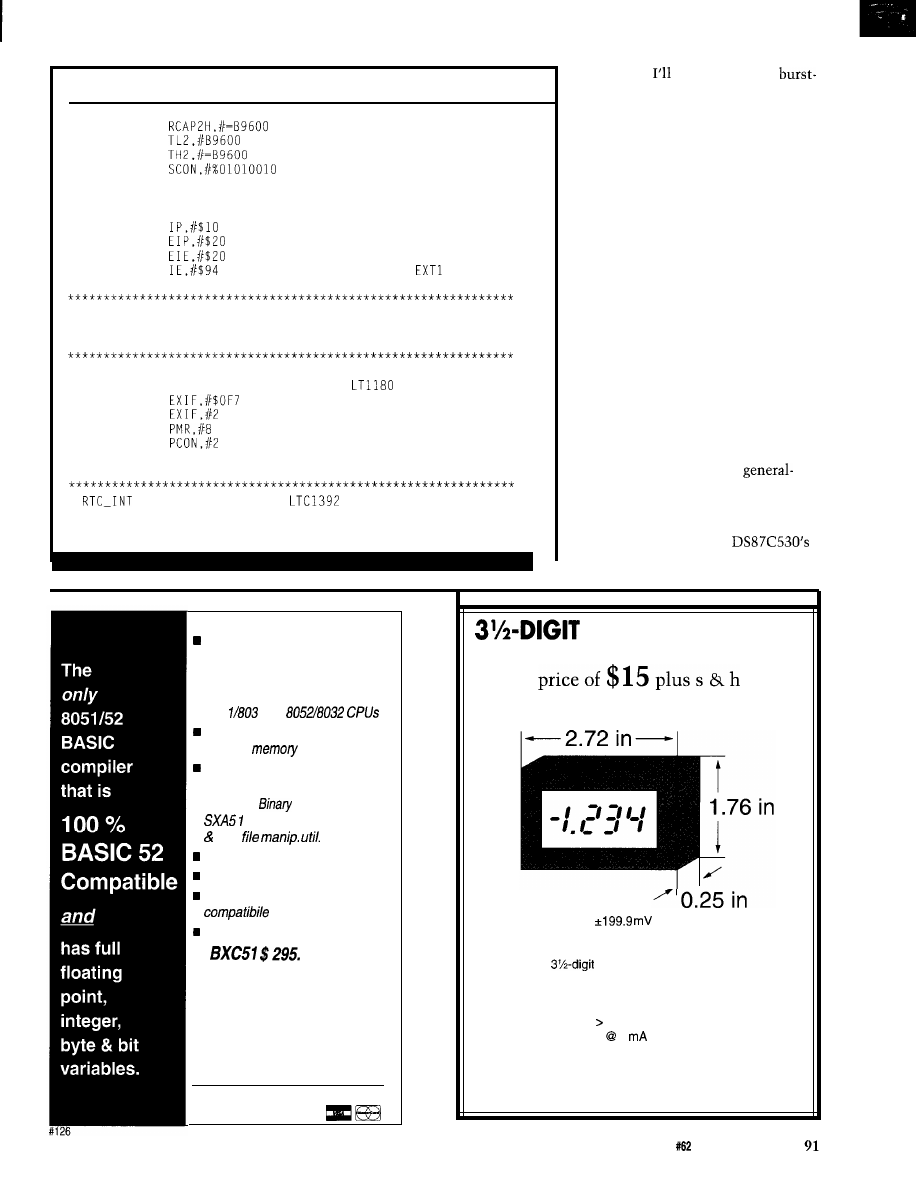
Listing l-continued
MOV
High baud reload
MOV
Low baud multiplier
MOV
High baud multiplier
MOV
Mode 1, REN. TXRDY, RXEMPTY
SETB T2CON.2
Enable baud timer
* Set up interrupts
MOV
Serial port 0: high priority
MOV
RTC: high priority
MOV
Enable RTC interupt
MOV
Enable SIO 0 and
interrupts
* MAIN waits for interrupts. When they are complete. it
* switches back to the ring oscillator and puts the
* part back into stop mode.
MAIN
CLR
EN232
Disable
ANL
Switch to ring oscillator
ORL
Enable restart from ring
ORL
Disable crystal
ORL
Enter stop mode
SJMP MAIN
*
reads a value on the
every 30 minutes, and
* logs data to the data buffer. When done, it returns to the
(continued)
performing,
concentrate on a
mode data-logging application. Al-
though the application runs and per-
forms something useful, keep in mind
that I’m keeping it extremely simple
in order not to obscure the power-
management theme.
A DIFFERENT DATA LOGGER
A traditional data-logger architec-
ture requires multiple switched power
supplies, external event-monitoring
circuitry, and discrete power-control
logic. In burst-mode operation, the
processor emerges from a fully pow-
ered-off state using dedicated power-
control circuitry. This wakeup is
usually controlled by some form of
periodic interval timer. Although
highly effective, this approach un-
avoidably increases component count
and cost. The cost penalty precludes
this type of instrument for
purpose applications.
In contrast, the system I’m pre-
senting attains equivalent burst-mode
capability using only the
inherent power-management features.
Memory mapped variables
n
In-line assembly language
option
n
Compile time switch to select
805
1 or
Compatible with any RAM
or ROM
mapping
Runs up to 50 times faster than
the MCS BASIC-52 interpreter.
n
Includes
Technology’s
cross-assembler
hex
Extensive documentation
Tutorial included
Runs on IBM-PC/XT or
Compatible with all 8051 variants
n
508-369-9556
FAX 508-369-9549
q
Binary Technology, Inc.
P.O. Box 541 . Carlisle, MA 0 1741
LCD PANEL METER
-Available now at an unheard of
N e w ! N o t s u r p l u s !
Specifications:
Maximum input:
additional ranges provided through
external resistor dividers
Display:
LCD, 0.5 in. figure height,
jumper-selectable decimal point
Conversion: Dual slope conversion, 2-3
readings per sec.
Input Impedance: 1 OOM ohm
Power: 9-12 VDC 1
DC
Circuit Cellar, Inc.
4
Park Street, Suite 12, Vernon, CT 06066
Tel: (203) 875-2751
Fax: (203) 872-2204
Circuit Cellar INK
Issue
September 1995
The trick to keeping power consump-
tion down is to build a system entirely
of micropower circuits.
To keep things simple, I added
only one part to the basic
system I presented last month. The
addition of Linear Technology’s
1392 thermometer, differential A/D
converter, and voltage monitor IC
provides the front end of a data-collec-
tion system in an
circuit.
Fully micropower, the LTC1392
typically requires 200
of current in
standby mode and 300
while
operating. The processor interface via a
synchronous serial link uses transmit
and receive data lines, a clock, and
chip select. Since communications are
defined as half duplex, the data lines
can be tied together resulting in a
three-wire interface.
The data format is compatible
with the Microwire and SPI interfaces.
Low power consumption combined
with serial operation offers the possi-
bility of locating this device remotely
from a processing unit if necessary. In
many applications, it’s advantageous
Listing l-continued
* main loop where it enters stop mode again. This simple
* example assumes that the system is read before
* the data overflows RAM, so no error checking is included.
*******************************X************************
ANL
Clear rtc interrupt flag
PUSH ACC
PUSH DPS
Save data pointer selector
MOV
Request temperature conversion
LCALL CONVERT
Acquire LTC1392 data
MOV
Switch to data pointer 0
XCH
Get msb
MOVX
Store to data buffer
INC
DPTR
Point to next location
MOV A,B
Get lsb
MOVX
Store to data buffer
INC
DPTR
Point to next location
XRL
Next interrupt in 30 minutes
POP
DPS
Restore data pointer selector
POP
ACC
RET1
*
causes the processor to download all stored data.
* It switches to the crystal first. The SENT bit indicates
* when all the data has been sent by the SIO ISR. This
(continued)
The BCC52 controller continues to be
Micromint’s best selling single-board com-
puter. Its cost-effective architecture needs
only a power supply and terminal to become
a complete development system or
board solution in an end-use system. The
BCC52 is programmable in BASIC-52, (a
fast, full floating point interpreted BASIC), or
assembly language.
The BCC52 contains five RAM/ROM
sockets, an “intelligent“
EPROM
programmer, three
parallel ports, an
auto-baud rate detect serial console port, a serial printer port, and much more.
CMOS
w/BASIC-52
l
Console
detect
.
printer RS-232
*Six interrupts
S-bit parallel
more!
. EXPANDABLE!
with 12 BCC
boards
B C C 5 2
Controller board
BASIC-52 and SK RAM
189.00
Single
Low-power CMOS version BCC52
$ 1 9 9 . 0 0
-40°C to
industrial temperature version
$ 2 9 4 . 0 0
BCC 52CX
Low-power CMOS, expanded
RAM
$ 2 5 9 . 0 0
CALL FOR OEM PRICING
4 Park Street, Vernon, CT 06066
Canada:
l
(3)
Welcome!
9 2
Issue
September 1995
Circuit Cellar INK
Requires
mtn.
RAM,
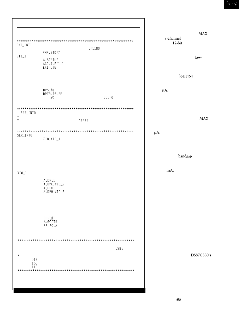
Listing
l-continued
* prevents the software from exiting the and reentering stop
* mode before all the data has been transmitted.
SETB
EN232
Enable
ANL
Enable crystal for serial activity
MOV
Wait until crystal has stabilized
JNB
ORL
Switch to the crystal
CLR
SENT
SETB TIO
JNB
SENT,*
MOV
MOV
MOV
DPS
RET1
Clear completion flag
Data will be sent by SIO ISR
Loop until all sent
Switch to dptrl and reset xmit ptr
Switch back to
to log data
*
handles serial port 0 interrupts. Serial port
interrupts are only possible when the system is "active"
following the assertion of the
bit. The primary
* function of this interrupt is to transmit the next
* character in the table until all data has been sent.
JB
* Receive interrupt
RINTO
CLR
RIO
RET1
Determine interrupt source
Clear receive interrupt flag
* Transmit interrupt
CLR
TIO
Clear transmit interrupt flag
MOV
Check for end of data
CJNE
MOV
CJNE
SETB SENT
RET1
Indicate completion
x10-2
PUSH
DPS
Preserve current data pointer
MOV
Switch to dptrl to track data ptr
MOVX
Still have data, xmit it, restore
MOV
Data ptr, return to send next byte
POP
DPS
RET1
* CONVERT data acquired using the LTC1392. The conversion
* command word is input in the accumulator. The two
are
* significant:
OOB Temperature conversion.
*
Power supply measurement.
*
Differential, 1-V full scale.
*
Differential, 0.5-V full scale.
CONVERT
* First, enable the LTC1392
SETB
?clk
Initial clock state
(continued,
to
put the sensing circuitry where the
action is.
Another front-end candidate
worth mentioning is Maxim’s
186. This
(4 if operated
differentially),
A/D converter
features a built-in 4.096-V reference
and has a Microwire/SPI-compatible
interface. Designed for very
power applications, the MAX186 has
several power-saving modes. Full
device shutdown can be invoked using
either an external
pin or a
command from the processor. In this
mode, power consumption drops to
about 2
This approach illustrates the
virtue of incorporating all converter
functions onto a single chip. Even a
micropower band-gap reference can
be a significant source of power con-
sumption considering that the
186 in fast shutdown mode (reference
enabled) has a power consumption of
30
For the most part, this value
represents the bandgap’s consumption
since all other device parameters are
identical to full shutdown in this
mode, except the
is not
disabled. When it becomes active, the
MAX186 is still no slouch, coming in
at just 1.5
You’d be hard pressed to find an
A/D converter that pulls so many
desirable features together. For applica-
tions needing an external reference or
for ratiometric applications, the
MAX188 provides identical features
without the built-in reference.
OPERATIONAL OVERVIEW
My data-logging application
operates under battery power, spending
most if its time in standby (Stop)
mode. This strategy brings power
consumption down to minuscule
levels. However, since the processor
oscillator is shut down, some external
method is needed to bring the system
back online. Because the
built-in, real-time clock runs from an
independent crystal, this “external”
wakeup is integrated right into the
processor.
The real-time clock periodically
generates an alarm interrupt which
takes the processor out of standby
Circuit Cellar INK
Issue
September 1995
9 3
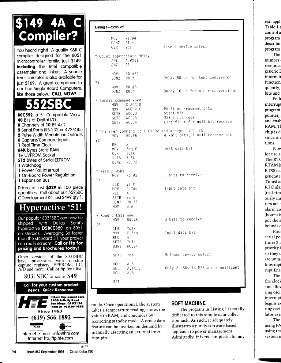
real application. For your reference,
Table 1 shows some of the clock
control and status bits relevant to the
program description. Let me begin by
describing functions of the various
program blocks.
The program starts by defining a
number of processor and application
resources. Since I am using Dunfield’s
generic
assembler, I first
inform it of the new
special
function registers
Subse-
quently, the application-specific I/O
bits and variables are defined.
Following the reset and (expanded)
interrupt-vector block, the executable
program begins setting up the stack
pointer, initializing processor I/O,
and enabling the 1 -KB embedded
RAM. The
RS-232 transceiver
chip is disabled to conserve power
since it is only needed for communica-
tions.
Now, the real-time clock is set up
for use as a periodic interrupt source.
The RTC alarm-compare
RTAM (minutes), RTAS (seconds), and
RTSS (subseconds)-are loaded to
generate an interrupt on the hour.
Timed access is required to enable the
RTC alarm capability through RTCC
(real-time clock control). The previ-
ously initialized alarm compare regis-
ters are set up to participate in the
alarm compare. Note that RTAH
(hours) is disregarded since it would
put the alarm interval beyond the
bounds of an hour.
Prior to entry into the main loop,
serial port 0 is initialized to run using
timer 2 as the baud clock. Interrupt
priority is given to the SIOO and RTC
so they can interrupt
Interrupts
are unmasked through the standard
Interrupt Enable and Extended Inter-
rupt Enable (EIE)
The main program loop switches
the clock source to the ring oscillator
and allows restart from Stop via the
ring oscillator through EXIF. On
interrupt, the processor immediately
begins executing under control of the
ring oscillator before the crystal oscil-
lator even starts up.
The crystal oscillator is disabled
using PMR, and Stop mode is invoked
using the familiar PCON SFR. The
system is now totally inoperative until
an interrupt occurs. As the ultimate
interrupt-driven system, it is quite
dead for the moment.
The system can now be enabled
via the real-time-clock interrupt or
through external interrupt 1. Normal
logging operations are handled in
response to an RTC interrupt. On
seizing control of the processor, the
RTC ISR proceeds by first clearing the
RTC interrupt flag. After pushing the
accumulator and data pointer select
register, the LTC1392 is accessed via
its serial support routine. When con-
version is complete, the appropriate
data pointer is selected and the 2-byte
(10 significant bits)
con-
version is stored.
Unmodified, the RTC causes the
next interrupt to occur on the hour
since a compare of RTAM (alarm
minutes) registers a match with
RTCM (real-time minutes) once an
hour. However, in this case, the de-
sired sample interval is 30 minutes. To
accomplish this, setting RTAM to 30
produces the desired result since
minutes are the qualifying parameter.
The simplest way to program a
recurrent, 30-minute interrupt is to set
RTAM to
(the RTC counts in
binary) when it is 0 and back to 0
when it is
Setting the interrupt
can be accomplished with the single
instruction XRL
, E.
The ISR concludes by restoring
the pushed registers and returns to the
main loop, which places the system
back into Stop mode. The ring oscilla-
tor provides the clock source for the
brief duration of the data-collection
sequence. The process concludes
before the crystal oscillator even has
time to warm up.
Asserting external interrupt 1
invokes the data-dump function. The
ISR begins by enabling the
RS-232 transceiver. This
enabling is done early to allow the
chip’s charge pump to ramp up the
positive and negative RS-232 rails.
Immediately following the charging,
the crystal amplifier is enabled since
serial communications are not possible
while using the ring oscillator. Further
processing is suspended until the
STATUS SFR indicates that the crystal
oscillator has stabilized and is
Circuit Cellar
INK
Issue September 1995
95
Bit
Location
Function
Reset
Write
name
access
EXIF.3
Crystal-Ring Clock Source Select
0 anytime;
0 = Select ring oscillator as clock source
1 when XTUP = 1
Select crystal or external clock as clock
and XTOFF 0
source
RGMD
EXIF.2
Ring/Oscillator Mode Status
0
None
0 Crystal or external clock is current clock
source
1 = Ring oscillator is current clock source
RGSL
EXIF.l
Ring Oscillator Select, Stop Mode
Unchanged
Unrestricted
0 = Crystal or external clock will be the clock
except after
source when resuming from Stop mode
power-on reset,
1 Ring oscillator will be the clock source
when it is
when resuming from Stop mode
cleared to 0
Note: Upon completion of crystal warm up
period, device will
to clock source
designated by
bit
XTOFF
PMR.3
Crystal Oscillator Disable
0 anytime;
0 Crystal oscillator is enabled
XT/% 0
1 Crystal oscillator is disabled. Device is
0
operating from ring oscillator
XTUP STATUS.4
Crystal Oscillator Warm Up Status
None
0 Oscillator warm up still in progress
1 = Oscillator warm up complete
Table
1-A look at the
new
reveals power
management
is
info the fundamental
architec-
ture.
able as the system’s primary clock
source.
At this time, the code falls
through and switches from the ring
oscillator to the more accurate crystal
time base. Directly setting serial port
O’s TIO interrupt flag transfers control
to the SIOO ISR. The code now stalls
while continually polling the Sent bit
which functions as the SIOO comple-
tion flag while the SIO ISR transmits
the stored data. It’s important not to
allow the
service routine to
terminate until the interrupt-driven
SIO activity completes since a return
to the main loop immediately takes
the system out of service.
On completion of the communica-
tions activity, the program drops
through and initializes the storage
pointer, effectively purging all stored
data in preparation for a new collec-
tion cycle.
AND THAT’S NOT ALL
Effective power management
dictates fitting the right power-control
techniques to a given application’s
specific requirements. The burst-mode
data collection I described is arguably
the simplest of all such applications
since it typically involves no real-time
processing whatsoever.
Things can and do get much more
complicated when you have to cut
power consumption and keep up with
real-world events at the same time.
Here, the wrong processor could easily
leave you out of options and out of
luck.
However, the
known
primarily for its high throughput,
won’t let you down when it comes
time to reduce the electric bill.
q
Dybowski is an engineer in-
volved in the design and manufacture
of embedded controllers and commu-
nications equipment with a special
focus on portable and
operated instruments..
Software for this article is avail-
able from the Circuit Cellar BBS
and on Software On Disk for this
issue. Please see the end of
for downloading
and ordering information.
431 Very Useful
432 Moderately Useful
433 Not Useful
Circuit Cellar INK
Issue
September 1995
9 7
The Circuit Cellar BBS
bps
24 hours/7 days a week
(203) 871-l 988-Four incoming lines
Internet E-mail:
Based on feedback I’ve received from readers, we have quite a few
ham radio operators out there (including our own Ed
Russ
Reiss, Harv Weiner, and John
This month, we
off with
a topic
may be familiar many of them: using
diodes for
doing switching.
Next, we’ve had a number of articles on motor speed control,
but here we look at dealing with higher voltages and AC versus DC.
If’s not as scary as you might think.
Finally, we fake a quick look at keyboard lock found on
almost of today’s IBM PC-compatible machines. if
a true
hardware-based lock?
PIN diodes as
switch
Msg#: 5906
From: David Gwillim To: All Users
have recently seen advertisements in ham radio maga-
zines for equipment using PIN diodes as transmit/receive
switches in linear amplifiers and finals for transceivers. The
PIN diode circuit apparently replaces a mechanical relay to
switch in and out the receiver connection to the antenna.
Does anyone have any circuits that perform this function
and any explanation of how they work?
I
would also be interested in supply houses that sell
parts (especially a line of PIN diodes that will function in
this type of circuit). All I know at present is that the acro-
nym PIN stands for Positive-Indium-Negative, referring to
the kind of junction in the diode, but I have no practical (or
theoretical for that matter!) experience with the device.
I was wanting to construct a
relay using a PIN
diode for use in a ham band
MHz) linear amplifier
operating at above 180 watts RF output.
The idea is quite simple, David. The diode exhibits a
relatively high impedance to an AC signal (if its voltage is
s u f f i c i e n t l y b e l o w i t s t u r n - o n v o l t a g e ) w h e n t h e d i o d e i s n o t
i s
forward biased, it looks like a
relatively low impedance to the AC component. This prop-
erty can be used to form a
switch, as you mention.
You can do this with any diode, though PIN diodes
perform better (don’t ask me why).
used to be
able from HP and others. I built a 2-m switch as you de-
scribe and operated it at about 100 W using nothing more
than
switching diodes, as I recall! The nice thing
about VHF/UHF, though, is that you can use quarter-wave
lines as impedance transformers, which allows you to place
the diodes at the optimum voltage/current peak/valley.
Often, more than one diode is used, some in series,
some in parallel. Some maybe driven on while the others
are driven off. With quarter-wave transformers, you can
create either an open or a short condition, as you wish.
I suggest you check the Radio Amateur’s Handbook
from ARRL (Newington, CT) first. I’d guess they must have
some of these circuits. Problem is, the contents change
yearly, so it depends a great deal on which issue you happen
to have access to. Also, there must be tons of references and
practical designs of these switches in QST, CQ, 73, and
Ham Radio (now defunct) magazines if you have access to a
library for back issues.
Msg#: 5955
From: David Gwillim To: Russ Reiss
Thanks for some insight into the theory. It makes sense
that that is how they operate. In all the years I did hardware
repair, though, I always found it was a long way from a
theoretical understanding of something to having a practi-
cal, efficient working circuit that doesn’t produce any
nasty, unwanted side effects! I will research the subject at
the library if I can get some back issues of ham mags there.
Msg#: 6114
From: Pellervo Kaskinen To: David Gwillim
may not have the latest catalogs on the areas of little
or no interest to my job. Microwave is one of those areas.
And microwave catalogs are the ones I would need to take a
look at for your PIN-diode-based
switch question.
The best I have available is an HP catalog from 1990.
There, the highest power offered is 120 W. Consequently,
then, it looks like just a couple of those diodes might do the
180 W you are asking for. But wait a moment!
The frequency range does not meet your requirements.
Not at the low end. The stated minimum frequencies for
most of the devices are either 30 or 50 MHz. The upper end
goes typically to 10,000 MHz. Maybe you should move up
to the
band?
Circuit Cellar INK
Issue
September 1995

Just kidding-like I said, I have not followed the trends
on this arena. Maybe newer devices really have improved
more than what is evident in my data sources.
I have another reason for my reply. PIN diodes are also
used in the optoelectronics (light waves). They are used in
fiber-optic signal receivers due to their fast response, low
noise, and excellent stability, All this is due to the “I” layer
that reduces the leakage current as well as the capacitance.
as switches for transceiver front-end filters. One of the
diodes tested was the
rectifier which has a
PIN structure. The
might be your cheapest, easiest
to get part. It should also be hard to kill.
I assume you want the PIN switch for full break-in. I’d
get hold of an ARRL handbook. My 1987 issue has plans for
a PIN
switch for a tube final transmitter. You could
probably modify the design for a solid-state final.
Ordinary PN junction devices with otherwise similar
geometries have a much higher capacitance unless they are
operated at very high reverse biases. And then they leak too
much, which means they are noisy. If the capacitance is
high, then the response speed is low. Basically, the same
issue you are dealing with in switch applications.
Personally, I always used a separate antenna or threw a
switch manually, but I’m not a CW demon!
Msg#: 5954
From: David Gwillim To: Chuck Olson
6157
From: David Gwillim To: Pellervo Kaskinen
Thanks for your input. Is there anything you don’t
involve yourself with? I see a lot of answers to people’s
questions coming from you. What business are you in?
I am just getting into ham radio and don’t yet have my
license (am taking the General exam soon). I had a lot of
interest in ham back in the early ’70s but was at sea then
and couldn’t easily get or use a ticket. My theory is pretty
good; just have to get my ear used to the dit-dahs again.
6162
From: Pellervo Kaskinen To: David Gwillim
I’m an electrical engineer, as in one trained for power
transmission and use of electricity. But all my professional
life I have been involved with electronics, control systems,
and measurements. It all started in manufacturing cables, or
actually making machinery for the cable manufacturing.
While I am getting ready for the license exam, I am
purchasing some ham gear. I bought an Index Labs QRP
Plus since small, neat packages really appeal to me, but I
wanted to hedge my bet with a few more watts of power. So
I bought a
linear parts kit for a
1.830-MHz
unit (their AN762). It doesn’t have a
relay, hence my
interest in PIN.
Next place I got into was a paper mill (of the same
company that owned the cable manufacturing). Besides a
paper mill, they had a pulp mill, a saw mill, a rubber prod-
ucts factory, and plastics factory on more or the less same
premises. Actually, we had a joint R&D center for the three
branches and I supported the measurement activities for all.
You are probably right about the Intrinsic instead on
Indium-it’s been a while since I did electronics seriously
(now have my own computer consulting business and do
financial software maintenance for a large bank).
5979
Then I got myself into a real adventure-it was as an
inspector abroad for a Finnish engineering company to in-
spect the quality of installations for a paper mill, pulp mill,
plywood mill, wood handling, steam power plant complex.
We had at peak 17 inspectors. The job lasted for 9 months.
From: Chuck Olson To: David Gwillim
Good luck on the test. I got my General about 20 years
ago. I still remember those “sweaty palms” at the Federal
building in Milwaukee.
I’d like to hear how your
amp works out. I’ve al-
ways meant to put some shoes on my Ten-Tee Argonaut.
Five watts is fun, but sometimes it’s nice to have the extra
power.
After that I came to the U.S. and started learning arc
welding. I still am trying to learn some of that after 16
years. Actually, I’m designing control circuits for welders
and accessories.
I’ve never heard of Index Labs. Is the QRP Plus a kit?
Msg#: 5992
From: David Gwillim To: Chuck Olson
5926
From: Chuck Olson To: David Gwillim
I thought PIN stood for P-doped, Intrinsic, N-doped. I
don’t have any first-hand experience with
but I under-
stand they will act as RF resistors with forward DC
more current, less resistance.
Index Labs is a small outfit in Washington state run by
a ham called Bruce Franklin. I get the feeling he has been in
the equipment design business a long time since the in-
nards of the QRP Plus are beautiful to behold! It isn’t a kit,
it’s a finished digital-synthesis QRP rig with full break-in
CW and SSB covering all HF ham bands. It has a built-in
iambic keyer, too.
There was an article in the December 1994 QST which
Index Labs advertises in CQ magazine and they had a
compared PIN and PN diodes for distortion characteristics
review of the rig in the October or November 1994 issue
100
Issue
September 1995
Circuit Cellar INK
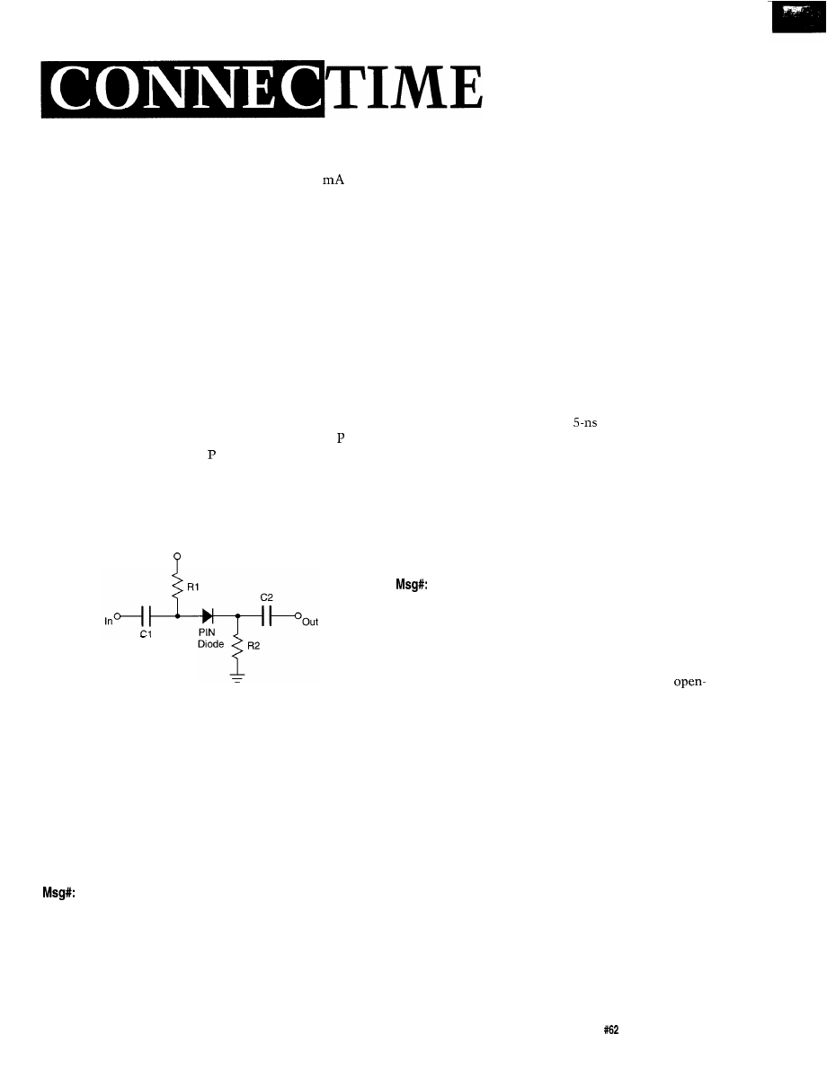
(can’t remember which). The little rig is really compact
(maybe 5” on a side in a cube) and pulls about 120
on
receive and about
1.5
A on transmit for 5-W output.
Since I don’t have my ticket yet, I had a friend try it out
for me and he was really impressed. A nice feature is that
Bruce built in a super-narrow CPU-controlled SCAF
(switched-capacitor audio filter) that gives you a brick-wall
bandwidth of anywhere from 100 Hz to 2400 Hz. You can
really peel apart CW with that.
If you are interested in seeing what makes the QRP
Plus tick, give Bruce a call at (206) 851-5725 and he’ll send
you an owner’s manual with circuit description and sche-
matics. You have to see the construction quality to believe
it, however.
Msg#: 5941
From: James Meyer To: David Gwillim
PIN stands for Positive, Intrinsic, Negative. The and
N are exactly the same as the and N used in NPN and
PNP when you refer to transistors. Intrinsic refers to a
semiconductor without any doping that would otherwise
have made it into a P-type or N-type.
Here’s a schematic of a PIN diode switch:
Bias
The RF flows from In to Out. A bias voltage is applied
so that when the bias is positive, the diode is forward biased
and RF flows from In to Out. When the bias is negative, the
diode is reverse biased and the RF is cut off.
The bias voltage needs to be larger than the applied RF
so that the diode stays either forward or reverse biased.
Switching lots of power isn’t very practical with PIN
diode switches. The resistors will eat up quite a bit of the
RF power. PIN diode switches are used at low power.
Simple, ain’t it?
5956
From: David Gwillim To: James Meyer
Thanks for the acronymic correction and the sche-
matic. It looks as though you need some added protection
circuitry in case the diode fails or there is a high enough
VSWR to turn it back on despite the bias (unless I am miss-
ing something). I am curious if you know why a PIN diode
is so special-maybe it’s got something to do with its re-
verse recovery speed or inter-electrode capacitance.
Msg#: 6011
From: James Meyer To: David Gwillim
My reply was purposely simplified to illustrate just the
basic idea of a diode switch. A real, useful switch would
require more parts depending on its application. For in-
stance, PIN diodes are often used as very high speed photo-
detectors as well as RF switches.
A PIN diode is special because it’s got very low leakage
in the reverse-biased condition along with low capacitance.
Some power rectifiers are made with a PIN structure. As far
as reverse recovery goes, PIN diodes are slower than equally
sized ordinary signal diodes. An HP PIN diode for RF use
will have a reverse recovery of around 100 ns as compared
to a similar-sized signal diode’s
reverse recovery.
For RF use, one of the things that makes PIN diodes
useful is their characteristic resistance. At RF frequencies,
you can make a PIN diode’s resistance look like anything
from near infinity to near zero just by changing the DC bias
current through it. Makes remote-controlled attenuators
easy to build.
For simple on/off switching circuits, ordinary diodes
often are a better choice.
5958
From: Russ Reiss To: James Meyer
The “heating of the resistors” can be eliminated by
using chokes instead. This is also where quarter-wave lines
can come in handy as long as the design only has to work
over a narrow bandwidth (like my 2-m unit). An “AC short
circuit” at the bias source end transforms into an
circuit at the RF switching point, and the losses become
negligible.
As for being a “low-power” device, not true. They have
been used up in the kilowatt range with proper design. I was
amazed how well the unit I constructed (from some kind of
ordinary diodes) worked at around 100 W. The trick is in
turning the diodes on during transmit. Then, residual recti-
fication doesn’t happen since the receive signal is never
great enough to forward bias the diodes. You just have to
ensure that you pump enough bias current through the
diodes that any AC/RF component doesn’t succeed in turn-
ing them back off again while transmitting. But if the diode
is slow enough (at the frequency employed), it has a hard
time doing this anyway.
Jim’s circuit is but a starting point using a single series
diode as a switch. You can add more series diodes for
greater isolation and diodes which shunt various paths to
ground for further protection. And, as I keep saying, you can
do real magic with diodes and quarter-wave transformers!
Circuit Cellar INK
Issue
September 1995
101

Msg#: 6012
From: James Meyer To: Russ Reiss
The “heating of the resistors” can be eliminated by
using chokes instead.
I realized this mere microseconds *after* I posted my
message.
Not to defend myself for saying
switches are only for low power (they
switch kilo-
watt levels), but in most cases they only have to actually
pass small amounts of power. Take the typical ham’s “CW
break-in”
switch, for example. The diode is in there
to isolate the receiver input from the transmitter output to
prevent overloading. The transmitter’s output normally
doesn’t pass directly through the diode part of the switch.
Motor speed control
Msg#: 5656
From: Dave Friedeck To: All Users
am working on a project that requires a microproces-
sor to control the speed of a 220-VAC universal (one with
brushes) motor. I need to reach full motor RPM, so an SCR
will not work, but some triac circuit should do the trick. I
hope to cycle an output pin off the micro at various duty
cycles to do the trick. Now the problem: I hate high volt-
ages and blowing up good microprocessors. Any ideas?
Msg#: 5775
From: Pellervo Kaskinen To: Dave Friedeck
Sounds like you are talking about a single SCR? If that
is true, then of course you would get the effect of half-wave
rectifying and lose much of the speed range unless you add
four diodes in a bridge. Then you could feed your motor
either with DC or AC as you prefer and still do with a
single SCR.
What I’m talking about is a connection of a single SCR
from the common cathodes (positive out terminal) of the
bridge to the common anodes (negative output terminal),
while connecting the AC load in series with the AC supply
and one of the two AC terminals of the bridge. It works if
you take care of the stray inductances and transient sup-
pression. Otherwise, the SCR may fail to turn off.
The same problem tends to plague the DC-load version.
There, the load is simply in series with the SCR inside the
diode bridge. I have once battled it and found that I had to
put a
capacitor across the 24-V transformer second-
ary before the SCR started turning off.
Due to the commutation issues, I prefer to use at least
two
(together with two diodes or with a center-tapped
102
September 1995
Circuit Cellar INK
transformer). Then I have a choice of adding an extra free-
wheeling diode or omitting it. I also could get the free-
wheeling effect if I connect the two diodes in series and the
two
in series to form my bridge. But, I generally like
the idea of connecting the cathodes of the
together so
the common-cathode point becomes the control-circuit
common.
Whatever bridge configuration you choose, the impor-
tant issue is providing a good gate drive at the correct times.
That translates to the following rules in my book:
l
The trigger circuits have to be synchronized to the line.
l
The gate drive circuits in most cases have to be isolated
from the power circuits. In case of the two SCR cathodes
tied together, you may be able to avoid this.
l
The gate pulses have to be sturdy enough to guarantee
proper firing of the SCR. This can be done with a
or
a PUT plus a transformer. I prefer a blocking oscillator
that produces a
pulse of about 7 V, A capability.
l
The control circuit has to cover the range of O-180” of
electrical as close as possible, without losing the syn-
chronizing.
l
The control circuit most likely should contain either
feedback or some linearization to make the output motor
speed a reasonably linear function of the input voltage.
l
You always need a good snubber network over each SCR.
They moderate the inductive kick that comes when an
SCR switches either on or off. They also may provide the
necessary initial current to keep an SCR turned on before
the current can start flowing through an inductive load,
although that purpose is better served with a longer gate
pulse. For most
a 15-25-p pulse does fine with a
resistive load, while 70 or more microseconds is required
for a partly inductive [motor) load.
Come to think of it, most of these rules are equally
valid for a triac use. The only difference may be that you are
likely to use the triac circuit for an AC motor.
There have been reports of poor results when trying to
control a ceiling fan speed with a triac circuit. One of the
main problems generally is that the triac trigger circuits are
not guaranteed to produce symmetrical positive and nega-
tive half cycles. In that respect, I’m still in favor of the
or four-element SCR bridge.
PC keyboard lock
5601
From: Calvin Krusen To: All Users
would like to know how the keyboard lock [the eleva-
tor style cylinder lock on the CPU box) is integrated into

the operating system. Does the POST use the state of this
to prevent the boot-up sequence, or is it something that can
work any time the PC is powered up?
What I would like to do is “Lock” the keyboard (of one
of our servers) so that “accidental” key strokes don’t cause
problems.
I was doing this for a while, but found that some times
after unlocking the keyboard, certain keys were remapped.
For example, the Num Lock key functioned as the Esc key
(Num Lock LED didn’t toggle when Num Lock key was
pressed]. Also, none of the cursor keys would work. I used
to do a cold boot (power off) to remedy this problem, but
later found that I only needed to momentarily disconnect
the keyboard connector.
Does the keyboard interface on the PC truly recognize
the keyswitch? Or
is
it that the keyswitch just breaks sev-
eral signals between the controller and the connector?
5629
From: Ed Nisley To: Calvin Krusen
It’s
worse than you think: the lock switch goes to
the keyboard controller. The controller is supposed to sup-
press keystrokes from the keyboard and ignore (most) corn-
mands from the system when the lock is active. There’s a
command bit that disables the lock function, which lets
the system send some commands and receive some re-
sponses even when the keyboard is “locked” at the front
panel.
It sounds like the BIOS and your keyboard controller
aren’t getting along well at all. My guess is that the control-
ler is ignoring a command that the BIOS thinks ought to
work fine; I haven’t a clue as to how you’d track that down,
though.
As to how the keys get remapped, that’s a
puzzle!
Msg#: 5779
From: Calvin Krusen To: Ed Nisley
Is
the above mentioned keyboard controller the one in
the PC or the one in the keyboard?
Also, I often find that a similar problem occurs after
running Central Point Backup (run on a daily basis). I no-
ticed that when CP Backup is running Ctrl-Alt-Del does not
work (had to try the old three finger solute many times).
How does the running program disable the Ctrl-Alt-Del? Is
it an operating system hook or direct mashing of hardware
registers (I’m guessing the keyboard controller has some
specific I/O for this function)?
Anyway, in a “working” system would it be normally
acceptable to disable the keyboard while either a program is
running, or just sitting at the DOS command prompt?
Msg#: 5788
From: Ed Nisley To: Calvin Krusen
Curiouser and curiouser!
I was thinking of the keyboard controller on the PC
system board, but it could also be the one out in the plank
if you’ve got a particularly bizarre clone. No way to tell.
The canonical way to “disable” the three-finger salute
is by hooking Int 8 and discarding the “third” keystroke.
There’s an official, documented, really-truly BIOS hook that
gives you access to all keystrokes after the BIOS processes
them and before it does anything, but I don’t know if that
function gives access to Ctrl-Alt-Del sequences.
In any event, there’s nothing specific in the keyboard
that makes Ctrl-Alt-Del do what it does. The BIOS defines
that function, which is why it doesn’t work when you’re
running, oh, say, some offbeat protected-mode code such as
you’ll see in a few months..
disabling the keyboard is rude, if only be-
cause it’s hard to do anything else after the program
crashes!
(Not much of an answer in there, I’ll admit. Sounds like
the only way to track it down is the relentless application
of logic, accompanied by swapping all the hardware in sight.
Phooey!)
We invite you to call the Circuit Cellar BBS and exchange
messages and files with other Circuit Cellar readers. It is
available 24 hours a day and may be reached at (203)
1988. Set your modem for 8 data bits, 1 stop bit, no parity,
and 300, 1200, 2400, 9600, or
bps. For information on
obtaining article software through the Internet, send
mail to
Software for the articles in this and past issues of
Circuit Cellar INK
may be downloaded from the Circuit
Cellar BBS free of charge. For those unable to download
files, the software is also available on one 360 KB IBM
PC-format disk for only $12.
To order Software on Disk, send check or money
order to: Circuit Cellar INK, Software On Disk, P.O.
Box 772, Vernon, CT 06066, or use your Visa or
Mastercard and call (203) 875-2199. Be sure to specify
the issue number of each disk you order. Please add $3
for shipping outside the U.S.
434
Very Useful
435 Moderately Useful
436 Not Useful
Circuit Cellar INK
Issue
September 1995
103
to Gambleticut
every region of the country has its never-ending news story. Every night, for what seems like
forever, the news always starts with the same old saga. Here in Connecticut, the big story for the last couple
years has been Indian Gambling (i.e.,
Resort Casino).
The only reason I mention this is because writing a serious editorial is being inhibited by fits of laughter about an earlier
computer adventure. Very few people know that one of my first “commercial” experiences with computers was gambling!
Back in 1977, while was working for Control Data Corp., my fellow worker Ralph conned me into letting him use my computer.
While we worked for a computer company, private access to one was another story. My full-blown
Digital Group
system
became the prime target of his scheme to run a betting-odds program and beat the bank at jai alai.
Eventually, weakened (ran out of excuses) to the constant hustle and agreed. For the next two weeks, my life was a disaster.
I thought I was the only pawn until the six members of Ralph’s SWAT (Special Wagering and Tactics) team arrived at my house after
work each day. Even though I loved to cook, two weeks of gourmet entertaining (Ralph liked to eat) made me feel like a cruise
director. When I wasn’t playing chef, was the computer’s field-service engineer.
Getting rid of these guys meant agreeing to move the computer to a motel next to the jai alai fronton. forgo the sordid details
associated with seven guys checking into a single motel room.
In any case, because the eight jai alai players and their statistics weren’t available until shortly before a game, the betting
program couldn’t be run until then either. Also, without the benefit of cellular faxes and phones, runners got the statistics and betting
calls back and forth between the fronton and the computer operator at the motel.
I’m not a gambler. I don’t even buy lottery tickets. The fact that I was involved in this at all was embarrassing enough.
I volunteered to stay in the motel while the others played runners. Ralph sat and played money man, of course.
Since I’ve always professed myself to be a hardware guy at heart, I never really thought too much about their betting algorithm.
I guess I just wanted to see if the hardware was up to it. At the appointed times, I entered the data and printed the computer’s
predictions for the order in which the eight players would end up. Ralph took the first three predictions and bet on them as a boxed
(any two of the six possible combinations) win, place, and show trifecta bet. Because this was still experimental, the bet was only $18
each time.
Each time I gave the runner a new printout, he’d give me the results of the previous set. Ralph had won $83 on the first game
but had lost the next six in a row. As I passed the predictions to the runner for the eighth game, I studied the results of the previous
seven and nearly fell off the chair.
While the win, place, and show numbers had only come up once in seven games, within the first three numbers in the
computer’s prediction, they came up five times in the fourth, fifth, and sixth predicted positions! When the runner came back with the
eighth game results, the trend held true again.
Seeing that three out of four games were being forecast correctly (albeit not directly) was too much. I instantly volunteered to be
the new fronton runner. Of course, I stopped at the trifecta betting window on each pass.
To make a long story fit one page, let me just say that by the end of the
evening, Ralph had lost $97. The good news
was that I had won $110 on the three games I played! Even so, I looked at it as an adventure, not a new profession. To this day, I
have never been back to jai alai again, nor have I ventured to Foxwoods. The businesses I’m already in involves about as much
gambling as I can take.
P.S.: be at the West Coast Embedded Systems Conference on September 12 and 13.
112
Issue September
1995
Circuit Cellar INK
Wyszukiwarka
Podobne podstrony:
circuit cellar1996 09
circuit cellar2004 09
circuit cellar1995 09
circuit cellar1997 09
circuit cellar2000 09
circuit cellar1993 09
circuit cellar2001 09
circuit cellar2002 09
circuit cellar2003 09
circuit cellar1994 09
circuit cellar1996 09
circuit cellar2003 09
circuit cellar1994 09
circuit cellar1997 09
circuit cellar1993 09
circuit cellar2004 09
circuit cellar1996 09
więcej podobnych podstron