Mainstream Processing
he proliferation of digital signal processing in
today’s mainstream society is truly astounding.
equipment for many years, but the true test of a
technology’s viability is when it is integrated into mass-produced consumer
equipment. Witness the enormous success of the compact disc over the last
years. It has revolutionized quality music reproduction and has breathed
new life into the recording industry. Signal processors that add
like ambiance to recorded sound have also taken off, thanks completely to
DSP.
I’ve always considered where I live to be somewhat “in the sticks.” We
live on a
road in a sparsely populated part of town. Imagine my surprise
when asked the telephone lineman down the street what he was doing and
he responded that he was activating a fiber-optic substation not 2500 feet
from my house. When (and if) SNET decides to implement
or some
other digital service, we’ll be close enough to a substation that subscribing to
the service should be painless. In the meantime, we have the benefit of
crystal-clear telephone service, thanks again to DSP.
We start off our signal processing issue with the question, can a RISC
processor do DSP as well as a dedicated DSP chip? In one of his “having
pun with a processor” articles, professor Michael Smith implements an FIR
filter on an Am29050 RISC processor, describes the development cycle he
went through, and explores its potential in DSP applications.
Next, we add some real-world interfaces to an off-the-shelf IBM PC
card and both control function generator chips and analyze incoming audio
signals, all using a desktop IBM PC.
In our third feature article, we turn our attention to neural networks and
how they can be used in everyday life. A single program can be written and
used for many situations by simply retraining that program for each instance.
In our columns, Ed’s embedded ‘386SX system gains a BIOS
extension to handle hardware the original PC designers never dreamed of.
He also passes on some valuable advice he learned in the trenches while
debugging an old project: Jeff has fitted last month’s optical ID card reader
with some glasses and boosts its resolution by an order of magnitude. Tom
checks out a pair of new one-time programmable processors that are small
in size and price. John describes several techniques for adding lots of
memory to small microcontrollers. Finally, Russ has searched his database
for spread-spectrum-related patents and has found some interesting tidbits.
JOURNAL
FOUNDER/EDITORIAL DIRECTOR
PUBLISHER
Steve Ciarcia
Daniel Rodrigues
EDITOR-IN-CHIEF
Ken Davidson
PUBLISHER’S ASSISTANT
Susan McGill
TECHNICAL EDITOR
Michael Swartzendruber
CIRCULATION COORDINATOR
Rose
ASSOCIATE EDITOR
Robert Rojas
CIRCULATION ASSISTANT
Barbara
ENGINEERING STAFF
Jeff Bachiochi
Ed
Nisley
CIRCULATION CONSULTANT
Gregory Spitzfaden
WEST
COAST EDITOR
Tom Cantrell
CONTRIBUTING EDITORS
John Dybowski Russ Reiss
BUSINESS MANAGER
Jeannette Walters
ADVERTISING COORDINATOR
Dan Gorsky
NEW PRODUCTS EDITOR
Weiner
ART DIRECTOR
Lisa Ferry
GRAPHIC ARTIST
Joseph Quinlan
CONTRIBUTORS:
Jon Elson
Tim
Frank Kuechmann
Pellervo Kaskinen
CIRCUIT CELLAR INK. THE COMPUTER APPLICA-
TIONS JOURNAL (ISSN 0896-8985) is published
monthly by
Cellar Incorporated, 4 Park Street.
Suite 20, Vernon. CT 06066 (203)
Second
Vernon.
One-year (12
USA and
tries $49.95. All
orders payable
funds only, international postal money order or
check draw” on U.S bank.
orders
and
related
to The Computer
Applications Journal
P 0 Box 7694,
NJ 08077 or call (609)
POSTMASTER: Please send address changes to The
Computer Applications Journal,
Dept.. P.O.
Box 7694,
NJ 08077
illustration by Bob Schuchman
PRINTED IN THE UNITED STATES
ASSOCIATES
NORTHEAST
Debra Andersen
Fax: (617) 769-8982
MID-ATLANTIC
Barbara Best
(908) 741-7744
Fax: (908) 741-6823
NATIONAL ADVERTISING REPRESENTATIVES
SOUTHEAST
Collins
WEST COAST
Barbara Jones
(305) 966-3939
Fax:
(305) 9858457
MIDWEST
Nanette Traetow
(708) 789-3080
Fax: (708) 789-3082
Shelley Rainey
(714)
Fax: (714)
parity. 1 stop
9600 bps Courier HST.
All programs and schematics
I
”
Cellar
been carefully
to
performance
transfer by subscribers.
“a
programs schematics or for the consequences of any such
Furthermore, because of
in
and
of materials and workmanship of reader-assembled
Circuit
INK
any
for the safe and proper
of reader-assembled projects based upon or from
plans,
or
published in
Cellar
INK
Entire contents copyright 1993 by
Cellar Incorporated. Ail
reserved.
of
in whole or in
without written consent from
Cellar
2
Issue
September 1993
The Computer Applications Journal
1 4
Is the AMD29050 a FIR-bearing Animal?
by Michael Smith
Using Your PC for Function Analysis
3 6
Neural Network Basics
by
Phillips
q
Firmware Furnace
Ticks, Pops, and Restarts: The ‘386SX Project
Gets a BIOS Extension
Ed Nisley
5 6
•J
From the Bench
Giving the Optical Card Reader Improved Vision
Bachiochi
6 4
q
Silicon Update
Penny-pinching
Tom Can
q
Embedded Techniques
Storage for the Masses
Dybowski
Letters to the Editor
edited by Harv Weiner
Steve’s Own INK
The Collegiate Challenge
The Computer Applications Journal
Issue
September 1993

The Sample Game Rules
As a hacker/entrepreneur, I read Steve Ciarcia’s
Please understand that Steve did not intend to let
comments about the “sample game” with much interest
the cat out of the bag on how to get unlimited, free
(“Steve’s Own INK,” February 1993). As a field
components from the distribution channel. He was
tion engineer for Bell Industries (an electronics
merely illustrating what happens when the focus shifts
tor) I can sympathize with his plight. I disagree with his
from “long-term engineering development and support”
solution, on a couple of counts.
to “nothing but the quota matters, don’t
bother
m e
First, understand that a distributor has direct and
unless you have a $10,000 order” mentality.
overhead expenses, just like your business. Every time
It seems the whole industry suffered when it was
the phone rings, it costs a distributor five bucks just to
taken over by the suits and bean counters. These folks
say hello. If the distributor is to break even
(not
make a
forgot (or never knew) what it’s like to develop a new
profit) he must sell at least fifty dollars worth of parts.
product on a limited budget, carve out a market for this
What Steve is suggesting is that you pull the wool
product, and after the course of a few quarters (or years),
over the distributor’s eyes (quite easy to do,
the payback for all of the efforts begins.
do a bluff, and get some “free” samples to boot.
Have the policy makers at
Electronics
Of course, it costs the distributor five bucks to answer
forgotten that HP and Apple were started by just two
the phone, three bucks to put the parts in the box, ten
engineers with stars in their eyes! Selling into these
bucks to ship the product, plus the cost the distributor
accounts is probably enough to have sales reps wrestling
paid for the product, but hey! What’s $18 among friends?
at the door. But what if these guys were trying to start
Fortunately, some distributors are getting more in
these ventures in today’s climate! Would they get parts!
step with the real world, just like Maxim and Dallas
Would there be anyone that could answer an even
Semiconductor. Instead of the $350 line item
minor technical question! Would the “I am only
mums, credit applications, and legal agreements that
interested- in sure things” mentality keep these guys
only lawyers can read, try calling the account
from getting the attention they need!
ment group of your local distributor.
You see, you
don’t know where the next Apple is
As an example, Bell Industries has a phone number
going to come from. And that is the risk you must
which allows you to use your credit
assume if you are going to be involved in this business.
card and requires only a $50 purchase. Do not expect
Hey, what’s $18 among friends! Okay, that’s justifiable.
technical support from these folks; their only function is
But, hey, make the guys at
Inc. upset with
to answer questions about price and take your order.
the whole way you do things, and maybe they’ll never
Most local distributors will also allow you to come
call you after they are placing those
orders.
in and pick up data books or data sheets, as long as you
And don’t forget that you guys provide service to
don’t abuse it. If you are truly working toward a product,
engineers, not bankers.
and not just fooling around, ask to talk to the FAE. As in
Granted, we should talk to the FAE. But truthfully,
any job, there are good ones and bad ones, some who
aren’t your attentions given due to the same “sales
have never actually built a circuit with their bare hands,
potential” criterion! We have had some close
and some who are up until 3
A
.
M
.
trying to get the damn
ships with sales reps and
and in our experience
thing to work, just like you and me.
the FAE is a limited resource under the direct control of
Just don’t expect miracles from distribution. Every
the sales department. If Bob the salesman says this
company
I
know of is trying to cut costs, and that means
must be done, then out of necessity, the question asked
those employees “lucky” enough to still be around end
by
Inc. goes to
the back
burner.
up timesharing between two or three jobs. I think you’ll
We are pleased to hear that new methods for
find there are distributors with decent salespeople, but
component purchase are being explored to keep the
the decent salespeople are not likely to go running after a
whole industry from becoming an “old boys club. This
five- or ten-piece order. You have had some unfortunate
is a step in the right direction, but now your
experiences with distribution, and I’m sure your opinion
tion has to make it easier to learn about it, not just buy.
is justified. Just don’t throw out the barrel because of one
As you can see this issue is an important one. The
or two rotten apples.
very forces of innovation are at stake. Let’s hope we
make the right moves, or we may all pay dearly for the
David Riness
wrong turns.
Cypress,
-Editors
6
Issue
September 1993
The Computer Applications Journal
More Chilling Thoughts
With regard to the question of how wind chill
factors were determined (“Reader’s INK,” The
Computer
Applications Journal, June
I read somewhere
several years ago that these factors were determined
empirically. The experiment was to take sausage-shaped
bags filled with water (about the size of an adult forearm)
and expose them to various subfreezing air temperatures
and wind speeds.
At each temperature to be tested, the reference test
was at zero wind speed, with the time to freezing
measured. Then the time to freezing was measured at
various combinations of temperature and wind speed. If,
for instance, the time to freezing at 20°F and 15 MPH
was the same as 0°F and 0 MPH, the wind chill at 20°F
and 15 MPH was said to be 0°F.
I’m sure much interpolation and extrapolation was
done to fill out the tables. The formula Dana Romero
lists looks like many such equations
I
saw when I took
Heat Transfer in college-the result of some deranged
curve-fitting program left to run on a VAX (then!)
overnight.
The method used to determine the wind chill
numbers does bring up questions as to their validity, or
at least applicability. As one weather reporter said, these
numbers are only valid if you’re naked in the shade. I
think the numbers are popular because they let people
brag about how tough they are-to be out when the wind
chill was 45 below zero..
Curt Wilson
Northridge,
We Want to Hear from You
We encourage our readers to write letters of praise,
condemnation, or suggestion to the editors of
the Computer Applications Journal. Send them to:
The Computer
Journal
letters to the Editor
4
Park Street
Vernon, CT 06066
FREE
CALL
HELP
PARADIGM LOCATE
l
PARADIGM TDREM
l
PARADIGM DEBUG
l
Comprehensive software development tools for
all Intel
and NEC V-Series
microprocessors.
l
Borland C++ and Microsoft C/C++ support
l
Choice of stand-alone or in-circuit emulator
debugging
l
Unlimited toll-free technical support
l
money-back guarantee
Call today for complete
product information and embedded system
application solutions. You won’t be disappointed!
Proven
for Embedded
C/C++ Developers
Paradigm Systems, 3301 Country Club Road,
Suite 2214,
NY 13760
TEL: (607)
FAX: (607) 748-5968
Trademarks are property of respective holders.
See us at
Embedded Systems Booth
The Computer Applications Journal
Issue
September 1993
7
Edited by Harv Weiner
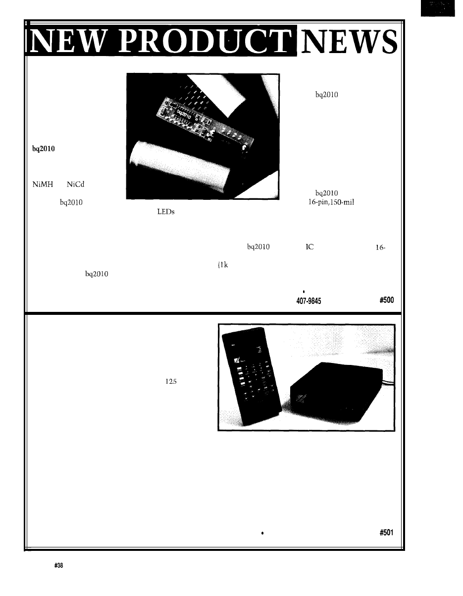
BATTERY CAPACITY
MONITOR
The first integrated
solution for comprehensive
monitoring of battery
capacity has been an-
nounced by Benchmarq
Microelectronics. The
Gas Gauge IC
provides accurate and
repeatable measurement of
the available charge in
and
recharge-
able batteries.
The
directly
displays available battery capacity using
and does
not require an external processor, allowing designers to
upgrade their systems to smart battery packs without
having to redesign the product. The battery’s charge state
and other battery-management information can also be
provided to a controller through a single-pin serial port
for a customized display.
Because the
is integrated within the battery
pack, critical capacity information is not lost with each
battery removal. External charge stations need not
provide tightly regulated charge currents and/or intelli-
gence to update the available
battery charge and capacity.
The
supports a
simple, single-line, bidirectional,
serial link to an external proces-
sor, and can output battery
information in response to
external commands over this
serial link. Internal registers
include available charge, tempera-
ture, capacity, battery ID, battery
status, and the settings of the
device’s programming pins.
The
is packaged in a
small,
SOIC. It,
and all of its necessary external components, can fit in
the crevice between two AA cells. This eliminates the
need to retool the plastics for the battery pack to accom-
modate the capacity monitor.
The
Gas Gauge
sells for $5.70 for a
pin narrow DIP and $5.90 for the 16-pin SOIC package
quantities). A development kit is available for $75.
Benchmarq Microelectronics, Inc.
2611 Westgrove Dr., Ste. 109 Carrollton, TX 75006
(214) 407-0011
l
Fax: (214)
MULTIROOM
ACCESS REMOTE CONTROL
The MARC (Multiroom Access Remote Control)
System enables the control of virtually any device from
any room in a house without wiring. Four kinds of infra-
red controlled audio/video equipment can be operated
with one remote control at distances up to
feet.
The MARC System can also operate up to 256 X-10
Powerhouse light, appliance, and security modules. For
additional security, each system has its own identifica-
tion code that is transferred with every button pressed.
The code can be established during initial setup and
changed as often as necessary. Expansion options include
an advanced security system, energy management,
telephone dial-in/dial-out support, and personal com-
puter interface modules to allow the design of a custom-
ized home automation system.
The MARC System is composed of a universal
remote control and a receiver. Depending on the button
selected, the receiver will do one of the following:
convert the RF signals into infrared signals to control
audio/video equipment, send commands over the power
lines for managing X-10 modules, or operate any of the
optional expansion modules.
The MARC receiver is designed to be placed behind
or beside the audio/video components. Because the
system is wireless, the equipment can also be installed
in an out-of-sight cabinet. The emitter is placed near or
over the infrared sensor window on the front panel of the
device to be controlled.
Vaux Electronics, Inc.
5310 Logan Ave. South
Minneapolis, MN 55419
(612) 920-5037 Fax: (612) 925-5175
8
Issue
September 1993
The Computer Applications Journal
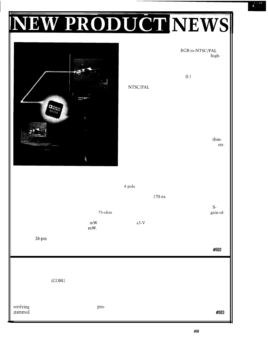
RGB-TO-NTSCIPAL ENCODER
The industry’s first analog
encoder provides video system designers with a
performance, fully calibrated, single-IC solution that
does not require discrete low-pass filters or delay lines.
The AD720 from Analog Devices features a composite
video output, a differential gain of
%, and a differen-
tial phase shift of 0.1”. This level of performance results
in
video outputs that are capable of generat-
ing smear-free reverse type (with text as small as 9
points) in applications such as PC video cards, multime-
dia systems, CATV converter boxes, and other video or
imaging systems.
The AD720 converts the red, green, and blue video
signals into their corresponding luminance (baseband
amplitude), chrominance (subcarrier amplitude and
phase), and composite (combined luminance and
chrominance) video signals. The AD720 produces
superior picture quality, largely due to the use of
film resistors in the RGB-to-YUV matrix, calibrated
board low-pass filters and delay line, and digitally
generated quadrature signals. In addition, the AD720
uses multiple ground and power supply pins to lower
internal package impedance, which can help prevent
crosstalk and signal feedthrough. This obviates the need for external adjustments.
The integration provided by three on-chip, low-pass filters and a delay line results in enhanced ease of use,
especially when compared to other discrete video encoding methods. No analog design experience is necessary to
implement the AD720 into a high-performance system. Two
filters bandlimit the U/V color-difference signals
to 1.2 MHz prior to subcarrier (color) quadrature modulation. A third 3-pole filter follows the modulator and limits
the harmonic content of the user-selected NTSC or PAL output. An on-board
delay function provides
precompensation for delays in the filters used to decode the NTSC or PAL signal in television receivers.
The separate luminance, chrominance, and composite output voltages are DC coupled, thereby providing
Video output. The AD720 is capable of driving
reverse-terminated loads through the use of on-board
two output amplifiers, which amplify the output voltage’s signal amplitudes to twice that of NTSC and PAL stan-
dards. The AD720 typically dissipates 200
(when powered with
supplies), and features a power down mode
that reduces consumption to less than 50
The power down mode is logic selectable and can be done whenever
the chip’s encoding function is not in use. All logic inputs are standard CMOS level compatible. The AD720 is
housed in a
plastic leaded chip carrier (PLCC) and sells for $18.39 in quantity.
Analog Devices, Inc
l
181 Ballardvale St.
l
Wilmington, MA 01887
l
(617) 937-1428
l
Fax: (617) 821-4273
LOW-COST PROGRAMMER
Single Chip Solutions has announced a low-cost
software, available from Motorola’s Freeware BBS.
programmer that connects to an IBM PC or compatible
The programmer is available as a kit or assembled.
through a serial port
or COM2). Power for the
Prices start at $100 for the kit. Programmers for the
PGMHC05 is provided by a 9-VDC wall transformer. All
MC68705 and MC68701 are also available.
programming voltages are generated and regulated on the
programmer board. The programmer is supplied with a
Single Chip Solutions
Windows interface that supports programming and
P.O. Box 680
l
New Hartford, CT 06057-0680
parts, as well as uploading data from
(203) 496-7794
parts. It is also compatible with the B U RN 0 5
The Computer Applications Journal
Issue
September 1993
9
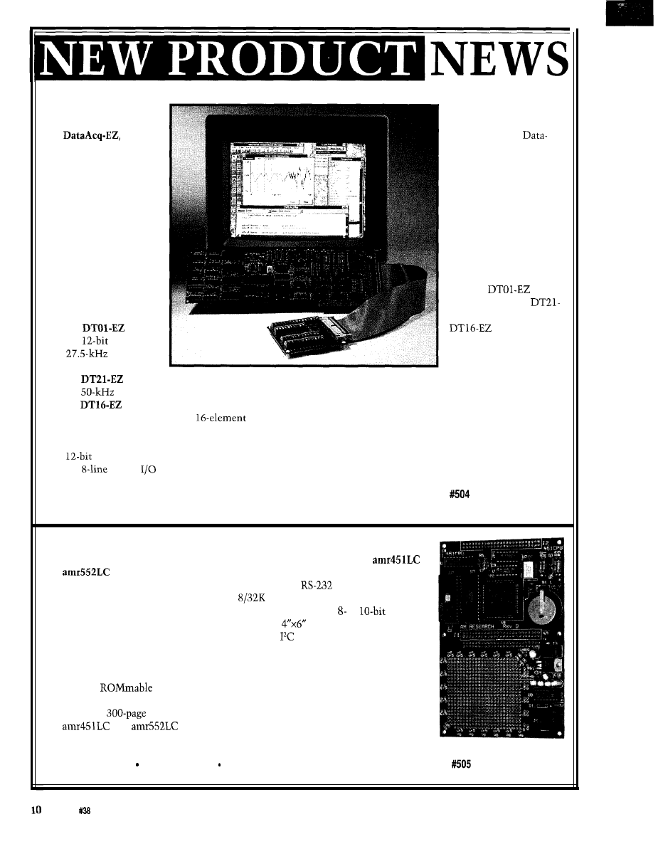
LOW-COST DATA
ACQUISITION
a low-
cost solution for Win-
dows-based data acquisi-
tion, has been an-
nounced by Data
Translation. Three data
acquisition boards with
varying resolutions and
speed are integrated with
the VB-EZ data acquisi-
tion programming tools
to easily create powerful
graphical and scientific
applications using Visual
Basic.
The
board
features
resolu-
tion,
through-
put, analog and digital
I/O; the
features
speed;
and the
increases resolution to
16
bits. Each board also
contains two indepen-
dent
D/A convert-
ers, two
digital
ports, software and/or
external triggering with
on-board clocking, and
can transfer data using
DMA. The DT2 1 -EZ also
offers random channel scan,
and a
channel/
gain list.
VB-EZ optimizes Visual
Basic for real-world data
acquisition by providing a
Data Acquisition Custom
Control. Using this Control
and the Visual Basic
constructs of Properties,
Events, and Methods,
simplifies hardware configu-
ration by insulating the user
from the complexity of the
I/O boards. A High-speed
Custom Control for plotting
quickly generates engineer-
ing and scientific graphs
that display acquired data in
real time.
VB-EZ supports all
analog and digital I/O
functions of the
Acq-EZ boards, and
includes subroutines and
function procedures that
perform buffer and data
management pertaining
to the specific board
installed. Context
sensitive help is available
at all times, supporting
all elements of program
development.
The
board
sells for $595; the
EZ for $795; and the
for $995. The
VB-EZ Visual Basic
Programming Tools sells
for $195, and the STP-EZ
Screw Terminal Panel
sells for $99.
Data Translation
100 Locke Dr.
Marlboro, MA 01752-l 192
(508) 481-3700
Fax: (508) 481-8620
LOW-COST MICROCONTROLLER
Two low-cost controllers have been introduced by AM Research. The
and
are embedded controllers which incorporate CMOS supersets of the
popular 805 1. These versatile microcontrollers contain an
serial port and +5-V
regulation. Other standard features include
RAM and ROM sockets; 56 and 48
I/O lines respectively; dual pulse width modulators; an g-channel, or
A/D
converter; a mailbox port; and a watchdog timer. The
boards also contain five
timer/counters with expanded compare functions, an
port, a prototyping area,
simplified expansion of up to an additional 256 bits of I/O, and a lithium battery for
RAM backup.
The systems includes an extensive array of software development tools which
can produce
Forth code. Other features are a full-screen editor, in-line
assembler, source-level single-step debugger, decompiler, disassembler, power source,
cabling, and a
manual.
The
and
each sell for $99.00. The systems sell for $199.
AM Research
4600 Hidden Oaks La. Loomis, CA 95650 (800) 949-8051
l
Fax: (916) 652-6642
Issue
September
1993
The Computer Applications Journal
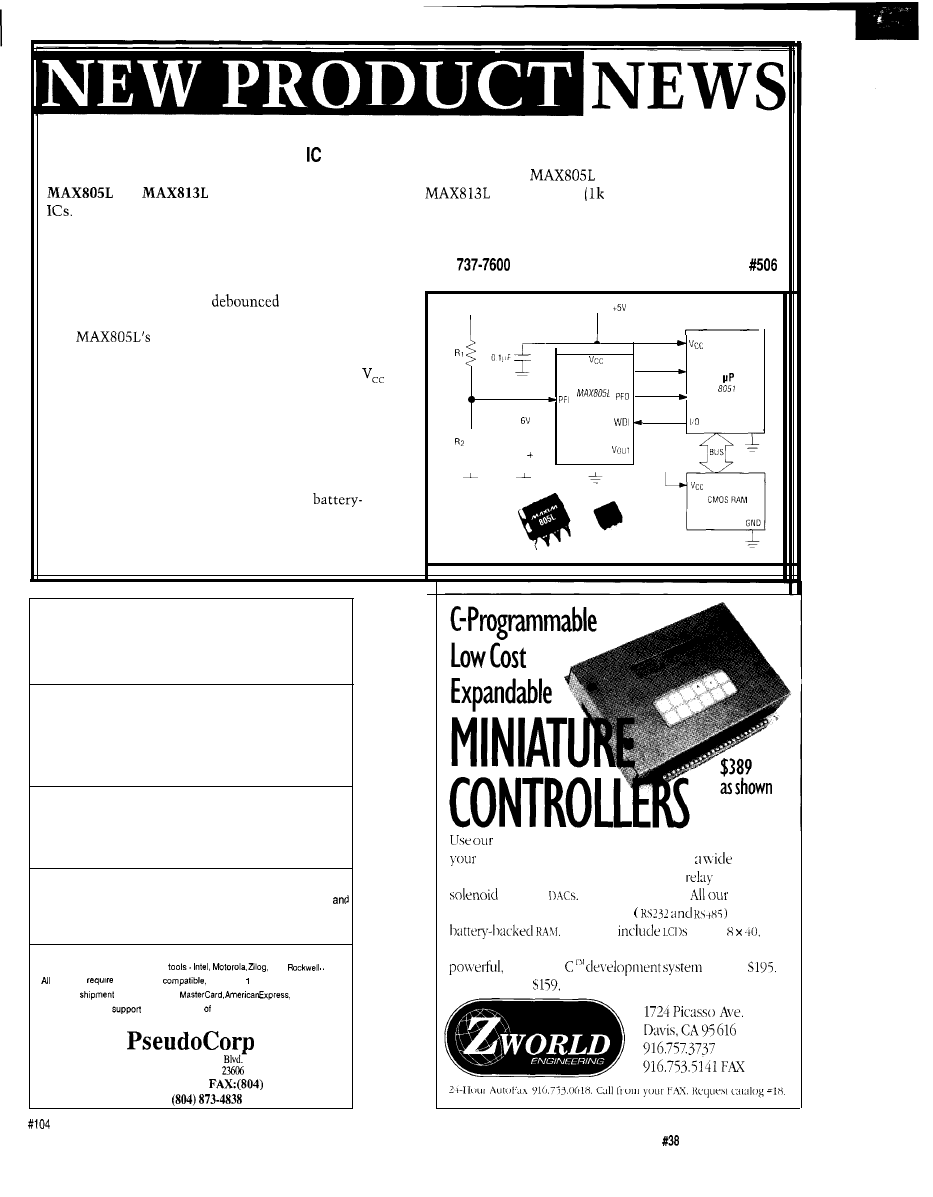
MICROPROCESSOR SUPERVISORY
Maxim Integrated Products has introduced the
and
microprocessor supervisory
They generate active-high reset outputs (RESET)
when V,. drops below 4.65 volts for all conditions of
power-up, power-down, brownout, and momentary power
interruptions. Active-high resets are required by many
Intel microprocessors, such as the 8051 series.
The MAX8 13L has a
manual-reset input
(MR) that is capable of generating resets on command,
The
battery switchover accommodates
backup battery power for SRAM and real-time clocks.
Reset pulses are 140 ms minimum, guaranteed for
as
low as 1 volt. Each device has an independent compara-
tor/reference circuit designed to monitor a battery, a
regulator input, or any other voltage. Each includes a
watchdog timer that monitors software execution by
issuing a reset whenever 1.6 seconds elapses without
evidence of activity on any selected I/O line.
Typical uses for these devices include
powered computers and controllers, intelligent instru-
ments, automotive systems, and critical microprocessor
power monitoring. Both chips come in either 8-pin DIP
or SOIC packages and are available in various tempera-
ture ranges. The
sells for $3.26 and the
sells for $1.61
quantities).
Maxim Integrated Products
120 San Gabriel Dr.
l
Sunnyvale, CA 94086
(408)
UNREGULATED DC
REGULATED
RESET
M A X I M
3
LITHIUM
BATTERY
VBATT
GND
T
I
RESET
NMI
LINE
GNC
Cross-Development
Tools
from $50.00
Cross Assemblers
Extensive arithmetic and logical operations
Powerful macro substitution capability
Unlimited include file capability
Selectable Intel hex or Motorola hex object file format
Simulators
Ten user-definable screens
Unlimited breakpoints and memory mapping
Trace file to record simulator session
Disassemblers
Automatic substitution of defined label names for all jumps
branches
Automatic insertion of supplied comments and expressions
Broad range of processor specific
R
CA,
products
a” IBM PC or
MS DOS 2 or greater
Same day
VISA,
and COD
Unlimited technical
Thousands satisified customers worldwide
716 Thimble Shoals
Newport News, VA
(804) 873-1947
873-2154
BBS
miniature controllers in your next product. in
plant or in your test department. Get
range
of analog and digital inputs and outputs.
and
drivers.
clocks and timers.
devices
provide serial communications
and
Options
up to
keypads. and expansion cards. Our easy-to-use. yet
Dynamic
is only
Prices start at
quantity one.
The Computer Applications Journal
Issue
September 1993
11
OPTICAL MEASUREMENT SYSTEM
An optical system for making distance measure-
ments has been announced by Acuity Research. This
system can precisely measure any distance from 0 to 20
meters. The AccuRange 3000 operates by emitting a
collimated laser beam that is reflected from the target
surface. The distance to the target is converted to a
frequency that may be precisely measured. The system is
suitable for a wide variety of distance measurement
applications that demand high accuracy and fast re-
sponse time.
The AccuRange 3000 has a standard deviation of the
indicated range as low as 0.25 mm. When calibrated, its
absolute accuracy and long-term drift have a standard
deviation of 2 mm when used with an infrared laser. The
nominal
range may be extended with
targets.
The sensor is 5.5 inches long and 3 inches in
diameter. It is housed in a rugged aluminum housing,
and weighs in at 18 ounces. Power requirements are 5 V
at 250
and 9-15 V at 50
Two versions are available: one with a visible red
beam and the other with a near-infrared beam. The IR
version has better sensitivity and lower measurement
noise, but the advantage of being able to see the beam
may be a more important factor in some applications.
The signal that represents the target’s range is
available from a BNC connector on the back panel. The
frequency varies from about 50 MHz (representing a zero
range) to 4 MHz (representing 20 meters). A Y-pin
connector is also provided for power and control signals.
A SCSI interface for the AccuRange is also available.
This board will connect to any computer with a SCSI
interface. It may be used as a stand-alone system, or it
can be installed in an IBM-compatible PC. The board
includes hardware for measuring the frequency and other
outputs of the AccuRange. The sampling rate is program-
mable, and can go as high as 3 12,500 samples per second.
The board also has precision power supplies for the
sensor, an input data buffer, and an optional
DC-motor control, and encoder sampling circuitry for
use in 3-D scanning systems.
Acuity Research, Inc.
20863 Stevens Creek Blvd., Ste. 200 Cupertino, CA 95014
(408) 252-9369 Fax: (408) 725-1580
TWO PROGRAMS FOR ONE LOW PRICE!!
SUPERSKETCH PCB
INTEGRATED
PCB II SUPERSKETCH features:
MOUSE DRIVEN *SUPPORTS
CGA, EGA, VGA SVGA,
* OUTPUT TO 9 24 PIN PRINTERS, HP LASERJET&
HPGL PLOTTERS * OUTPUT TO DTP PACKAGES *
* PCB II ALSO HAS GERBER OUTPUT VIEWING. *
THE EASIESTTO
R4 SYSTEMS, Inc.
1111 Davis Drive, Suite 30-332
Newmarket, Ontario
(416) 898-0665
fax (416) 836-0274
ALL PRICES ARE IN US FUNDS, PLEASE INCLUDE $7 S/H
. 1 2 Year Warranty
l
Technical Support by phone
l
30 day Money Back Guarantee
. FREE software upgrades available BBS
l
Demo SW via BBS
(PBlOOEMO.EXE)
l
2716
16
l
Flash
(EMP-20 only))
l
Micros
42A.
12
Issue
September
1993
The Computer Applications Journal
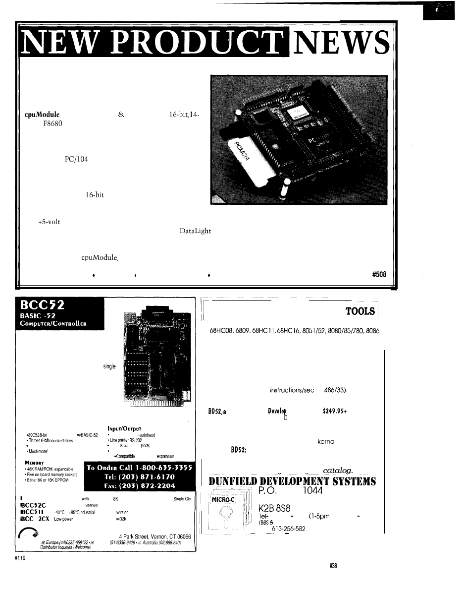
ULTRA-COMPACT COMPUTER
Real Time Devices has announced an ultra-compact
PC compatible, single-board computer measuring 3.8” x
3.6” and weighing only three ounces. The CMF8680
is based on Chips Technology’s
MHz,
PC/Chip processor. It was designed for
embedded applications requiring 100% PC software
compatibility, but where traditional PCs were too large,
power hungry, and unreliable. The CMF8680 is compat-
ible with the
form factor for embedded PCs and
can be expanded with any peripheral that is compliant
with this standard.
The CMF8680 includes a CGA graphics display port,
an LCD interface, a
IDE hard drive controller, a
high-density floppy controller, and a PCMCIA interface.
It features a full complement of standard PC peripherals. For software development, a keyboard, CRT, mass storage
and
supply are required to make the CMF8680 a fully functional industry-standard PC.
Each CMF8680 includes a standard BIOS and
ROM-DOS 5.0 kernel, and supports 1 MB of bootable,
solid-state disk. Included with the system are utility programs allowing users to put their application software in
ROM.
TheCMF8680
including 2M RAM, utility ROM, and support software sells for $895.
Real Time Devices, Inc P.O. Box 906 State College, PA 16804 (814) 234-8087
l
Fax: (814) 234-5218
The BCC52 controller continues to be
Micromint’s best selling single-board com-
puter. Its cost-effective architecture needs
only a power supply and terminal to become
a complete development system or
board solution in an
end-use system. The
BCC52 is programmable in BASIC-52, (a
fast, full floating point interpreted BASIC), or
assembly language.
The BCC52 contains five RAM/ROM
sockets, an “intelligent” 27641128 EPROM
programmer, three d-bit parallel ports, an
auto-baud rate detect serial console port, a serial printer port, and much more.
PROCESSOR
CMOS processor
Console RS232
detect
Six interrupts
Three
parallel
EXPANDABLE1
with 12 BCC
boards
BCC52
Controller board
BASIC-52 and RAM
$1
89.00
Low-power CMOS
of the BCC52
$199.00
to
temperature
$294.00
5
CMOS, expanded BCC52
RAM
$259.00
CALL FOR OEM PRICING
MICROMINT, INC.
Canada.
LOW COST DEVELOPMENT
We have a complete line of ‘C’ compilers (MICRO-C) for:
and
8096
processors. Cross assemblers for these plus others.
Source code and porting packages are available!
Development Kits:
$99.95 +
s&h
Includes C compiler, Cross assembler, ROM Debug monitor,
Library source code, Editor, Telecomm program and every-
thing else you need to do ‘C’ and Assembly language
software development for your choice of processor.
Emily52, a high speed 8052 simulator: $49.95 + s&h
High speed (500,000
on
Hardware
emulation mode accesses real ports/timers on your target
system. Includes PC hosted ‘in circuit’ debugger.
complete 8052
Everything you need for 8
ment System:
s&h
52 development, including:
Hardware: 8032 based single board computer with 32K
ROM, 32K RAM, RS-232 port, Hardware debug support.
Software: DDS MICRO-C Developers Kit, EMILY52 Simulator,
PC Hosted “in circuit” debugger and
in ROM.
loaded
$299.95 + s&h
As above, with extra 32K RAM, 4 A/D + 1 D/A, 2K EEPROM,
7 line relay driver, watchdog and power monitor.,
Call or write for our free
Box 3
N e p e a n , O n t a r i o C a n a d a
613 256 5820
EST, Mon Thu)
Catalog
R e q u e s t s
24
Hour with Touch Tone)
Fax:
1 (24 Hour)
The Computer Applications Journal
Issue September 1993
13
Is the AMD29050 a
FIR-bearing Animal?
Using Your PC for
Function Analysis
and Control
Neural Network Basics
Am29050 a
FIR-bearing
Animal?
Michael Smith
becoming increas-
because they can be
used to remove undesired noise from
sampled data. Off-line processing is
performed on stored data, and because
of the amount of data, requires rapid
processing. On-line filtering requires
real-time processing of an incoming
signal. Slow algorithms have no place
in these situations.
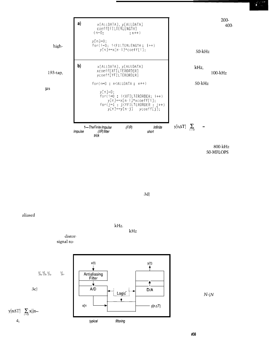
A couple of psuedocode examples
of typical digital filter algorithms are
shown in Figure
1.
Figure la shows an
FIR (Finite Impulse Response) filter,
and Figure shows an IIR (Infinite
Impulse Response) filter. Note that the
IIR filter uses a recursive algorithm,
which places some specialized restric-
tions on the processors used in real-
time applications.
In this article, I’ll concentrate on
on-line FIR processing. After all, off-
line data is simply yesterday’s on-line
data. The only difference in these two
systems is that off-line processes do
not have to meet stringent
times. What you can do in real time,
you certainly can do when you can
take your time. Figure 2 shows a
typical on-line digital filter system.
Although not specifically designed
for DSP, the Advanced Micro Devices
Am29050 floating-point RISC proces-
sor has features that make it suitable
for DSP. It includes a single-cycle FPU,
modulo arithmetic addresssing logic,
and data paths and
capable of
parallel operation. Its RISC architec-
ture and internal pipelines allow you
to write highly efficient programs.
I’ll show you features of the
Am29050 that can overcome the
14
Issue
September 1993
The Computer Applications Journal
problems associated with
implementing FIR filters, and
limitations of the chip that
require special attention. I’ll
discuss stategies that allow the
Am29050 to be used for
speed filters. These include
designing hardware for maxi-
mum throughput and the use of
decimation techniques. It’s
possible to produce a
linear-phase, single-processor,
FIR filter with a maximum
sampling rate of 2.6 when
four-fold FIR decimation
techniques are applied.
PRACTICAL APPLICATION
OF AN FIR FILTER
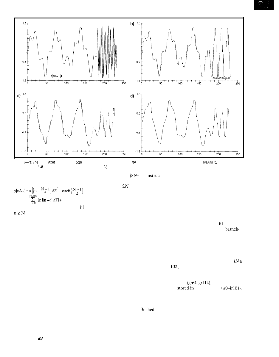
Figure 3 shows the various
stages of digital filtering. Figure
3a shows a signal that contains
high- and low-frequency
components. Figure 3b shows
float
float
for
n<ALLDATA
float
float
float
*
the digitized signal. Note that initially,
the digitized signal faithfully records
the signal. In the last part of the signal,
aliasing occurred during sampling and
the high-frequency signal has become
a low-frequency digital signal. Once
aliasing has occurred, there is very
little chance it can be reversed.
The digital signal can only
accurately represent the input signal if
the input signal does not have signal
components above the Nyquist
criterion. Signals above this frequency
will be
into lower frequencies
causing distortion. Many signals are
naturally limited, but wide-band noise
may be present. Aliasing this noise
does not necessarily introduce
tion, but it can reduce the
noise ratio. Adding a low-pass filter
would prevent this problem.
The calculations must complete
between samples for a real-time filter.
Long filter lengths place heavy
requirements on the processor. The
infinite amount of input in an on-line
filter causes a storage problem for
these systems and often, circular
buffers must be implemented, which
create considerable overhead. Finally,
the analog output signal [Figure
is
produced by routing the output
through a low-pass filter.
Decimation techniques are used to
speed up digital filters. Suppose the
input signal had frequency compo-
nents up to 400
This would
require sampling at 800
(or
greater) to remove aliasing. About 400
summations and multiplications must
be performed between each sample. If
This signal is then filtered
with a four-tap, symmetric,
low-pass FIR filter whose
coefficients are and
Symmetric filters reduce filter
distortion. The output of the
filter (Figure
is produced by
implementing the following
equation on all input values:
A 200-tap filter with an
sampling rate requires a
processor when four-fold decimation is
used. The Am29050 can provide 80
MFLOPS at 40 MHz provided the
pipeline can be kept full. Pipelining is
the concept of splitting an operation
into many steps that can be completed
in parallel. With this technique, a new
operation can start, or complete, every
cycle. This gives pipelined processors
their advantage. On a RISC processor,
the pipeline is king, and any instruc-
tion that detracts from the pipeline
performance is not implemented. Peak
performance is obtained when the
algorithm keeps the pipeline(s) full.
Although only one out of eight
output values are evaluated for a
decimation filter, all of the input
values must be processed. For
time-critical situations, a FIFO
stack attached to the ADC
relieves the processor of the
interrupt service overhead.
N - l
Analog Input
Signal
Analog Output Signal
Low-Pass
Filter
Converter
Timing
Converter
Digital
Input
Digital
AT]
P r o c e s s o r
Output
Figure
Response
filter (a) and the
Response
(b) can be described by very
algorithms. The
comes in implementing them efficient/y.
=
i) AT] x coeff [i]
N = n = 1, 2, 3, . . .
Figure 2-A
on-line digital
system.
this were attempted for a
tap filter, you would need a
MFLOPS processor! This class
of processor is not cheap or easy
to come by.
The output signal might
only need a
bandwidth.
However the output signal is
still produced with a sampling
rate of 800
which is
unnecessary since a
output rate would accurately
represent a
signal. You
could process one out of every
eight samples and still get an
accurate representation of the
output signal. Using decima-
tion, the filter’s equation now
looks like the following:
N - l
= x[(n i) AT] x coeff [i]
n = 1, 9, 17, . . .
IMPLEMENTING AN
FIR FILTER
I coded the odd) tap,
symmetric FIR filter algorithm
shown in the equation below
in a straightforward way. I’ll
discuss the problems that this
approach caused and how the
The Computer Applications Journal
Issue September 1993
15
a)
0.5
0.5
Figure
analog
signal contains
high-
and low-frequency components. When digitized, the high-frequency signal is lost to
The digital output
of the filter shows
on/y the lower frequencies have been passed. The final analog output shows the filtered signal.
various features of the chip allowed
me to get a more efficient algorithm.
x
x [(n N + i) AT]) x coeff
The first part of Listing 1 shows
the full C code for an on-line FIR filter.
The second part is a direct translation
of this code into Am29050 assembler.
The program starts by initializing
pointers that are used to bring in data
and filter coefficients from memory.
Then follows a loop to bring in the
data and coefficients from external
memory to implement the filter.
One difference between on- and
off-line filtering is the need to service
the A/D and D/A converters. Less
obvious is that the real-time loop will
be slower because of the overhead of
the circular buffer, since the data must
remain within the bounds of a fixed
memory array.
If I assume that the CHECKADJUST
macro takes four instructions, the real-
time FIR filter takes
15)
operations. The program is very
inefficient, especially if I account for
tions. This is a considerable period of
the possibility of wait states and the
problem of keeping the pipelines full.
To improve the efficiency, I wrote the
time to perform
floating-point
code again, taking into account the
architectural features of the Am29050.
The Am29050 has 192 registers
which can be used as a cache. Since
the filter coefficients are unchanging,
it would make sense to store these in
the on-board registers. The chip also
has separate data and instruction buses
so I can load data during instruction
execution.
associated with the circular buffer that
occurs during address calculations.
most recent branches and reduces
The memory management unit can
perform this process in parallel with
instruction pipeline stalls.
other operations, giving a significant
performance improvement. I can also
A major problem is the overhead
gain speed with the ASS E instruc-
tion, which does single-cycle
and-test during address pointer checks.
The program causes frequent
pipeline stalls. This is particularly true
for floating-point operations where the
pipeline is six stages deep. By rearrang-
ing the code, I can keep the pipelines
full and gain considerable speed.
Each branch will cause the
instruction pipeline to be
which causes it to stall. Activating the
on-board branch target cache (BTC)
stores the instructions following the
DATA CACHE FULLY ON-BOARD
THE INTERNAL AM29050
REGISTERS
If the number of taps is small
it is possible to store all data and
coefficients on-board. The filter
coefficients are stored using global
registers
The data values
are
local registers
The more-optimized code for imple-
menting a real-time FIR filter for this
situation is shown in Listing 2. Data
values are placed in local register
window. This avoids the overhead of a
circular buffer, because the local
registers in conjunction with the
16
Issue
September 1993
The Computer Applications Journal
The New Shape
of
Embedded PCs
The amazing
is
complete
100% PC-compatible
single board computer
measuring only 3.6” by
n
14 MHz
n CGA/LCD controller
n 2M DRAM
n ROM-DOS kernel
n bootable 1 M solid-state disk
n configuration EEPROM
IDE controller floppy interface
n PCMCIA interface
n two RS-232, one RS-485 parallel
n XT keyboard speaker port
n watchdog timer
n volts only operation
Designed for low power applications,
the
draws one watt of power,
which drops to 350 milliwatts in sleep
mode, 125 milliwatts in suspend mode.
Free
utility software lets your
application boot
from
ROM!
RTD also offers a complete line of
PC/l 04 peripherals for expansion:
n 1.8” hard drive PCMCIA carriers
n
14-bit data acquisition modules
n opto-22 digital
modules
n VGA CRT/LCD interface
For more information:
call, write
us today!
Place your order now and receive a
CM102 PCMCIA carrier module
FREE!
Listing
first
the C implementation
while the
the same
algorithm
in Am29050 assembler. direct approach causes stalls in the data, andinstruction
pipelines and results in a grossly
.cputype 29050
ASSUME NUMTAPS IS ODD
float
+ NUMTAPS
float
*xrecentpt. *xancientpt,
*coeffpt
float *buffstart, *buffend;
float yn;
xstart = xarray NUMTAPS
buffstart = xarray;
= xarray +
1
for
yn = 0;
coeffpt = coeffarray;
xrecentpt = xstart:
/*avoid range problems*/
/*establish pointers*/
xancientpt = xrecentpt NUMTAPS 1;
if (xancientpt buffstart) xancientpt += BUFFSIZE:
= (float)
for = 0; i NUMTAPS 2;
do FIR
yn += *xrecentpt- * coeffpt; /*worry about wrap*/
if (xrecentpt buffstart) xrecentpt =
yn += *xancientpt++ * *coeffpt++:
if (xancientpt
xancientpt = buffstart;
yn
* *coeffpt
tap*/
if (xstart
xstart = buffstart:
Array info
.set
FPACC. 0
which FP
to use
SETVALUES
initialize values
LOOP:
fmac
FPACC, ZERO, ZERO = 0
or
COEFFPT, COEFFARRAY, 0
coeffpt = coeffarray
or
XRECENTPT, XSTART, 0
xrecentpt = xstart
LCONST
XANCIENTPT. NUMTAPS
sub
XANCIENTPT, XANCIENTPT, 1
srl
XANCIENTPT, XANCIENTPT, 2
turn into a byte offset
sub
XANCIENTPT, XRECENTPT, XANCIENTPT
CHECKADJUST XANCIENTPT
load
0, XVALUE,
= (float)
convert XVALUE, XVALUE, SIGNEDDINT, NEAREST.
INT
store
0, 0, XVALUE, XSTART
rep
(NUMTAPS
0, 0. COEFF, COEFFPT
coeff =
add
COEFFPT, COEFFPT. 4
load
0, 0, XVALUE, XRECENTPT yn +=
coeff
sub
XRECENTPT. XRECENTPT. 4
fmac
FPACC, XVALUE, COEFF
CHECKADJUST XRECENTPT
load
0, 0, XVALUE, XANCIENTPT
yn += *xancientpt++ * coeff
Real Time Devices, Inc.
P.O.
Box
906
State College, PA 16804
(814) 234-8087
n Fax: (814) 234-5218
18
Issue
September 1993
The
Applications
Journal
register stack pointer
(grl)
automatically form a circular buffer.
Although there are now only one
eighth of the original number of
instructions, the speed is only a factor
of two faster. This is because removing
the circular buffer exposed inefficien-
cies in how I used the FPU. By keeping
the FPU pipeline full, this code could
run in
instructions and take
only
cycles. This is a 800%
speed advantage over the first method
of implementing the filter.
DATA CACHE PARTIALLY
ON-BOARD THE INTERNAL
AM29050 REGISTERS
When the number of taps is large
it is not possible to store
data and filter coefficients on chip.
Therefore, memory accesses are
required. Next I show how to over-
come many memory access problems
related to Listing 1 and some hidden
problems in using on-board registers
and the FPU as related to Listing 2.
Considerable overhead is associ-
ated with updating data pointers. The
Am29050 has a short machine cycle,
and does not implement an
autoincrementing address register.
Address calculations can be performed
using hardware that operates in
parallel with other facilities. This
capability is used with the load
multiple (LOADM) instruction, which
has the capability of transferring a
memory block to a register block. This
overlaps an implicit autoincrement
calculation with data fetches.
The READBLOCK macro reads in
NUMB E R data values from a memory
block pointed to by ADD R E S S
REGISTER into registers starting at
DATAREGISTERasshowninListing3.
The Am29050 is a 40-MHz chip
and it is expensive to implement
wait-state memory for this processor
speed. Instead, consider burst
memory-where after an initial wait
from the first read request, data is
available each cycle. The macro
READBLOCK
LOADM instruc-
tion, so it makes efficient use of burst
mode memory. The instruction
prefetch buffer
is designed to allow
burst memory. This reduces memory
speed requirements and design cost.
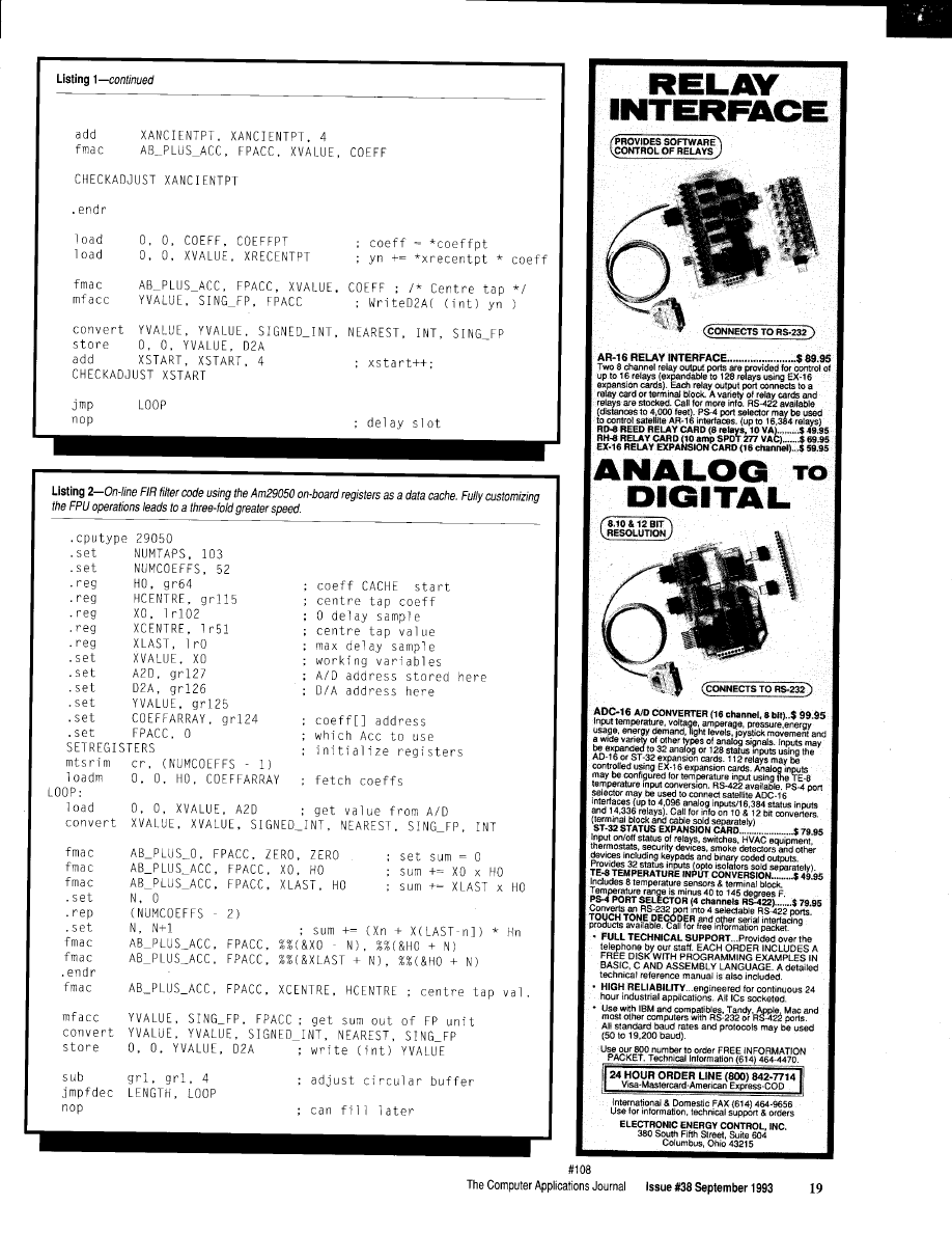
Listing
read; NUMBER
data
values from a memory
into
at
The
macro multiplies NUMBER data
values
stored at register
with the coefficients stored at register
m a c r o
READBLOCK, DATAREGISTER, ADDRESSREGISTER, NUMBER
mtrsim
cr, (NUMBER
load address counter
Round them up, move them in
loadm
0, 0, DATAREGISTER, ADDRESSREGISTER
.endm
macro
DSTART, CSTART, NUMBER, DIRECTION
FPACC, -1
NUMBER
N,
FPACC,
%
which Accumulator
FMAC
FPACC,
.endr
.endm
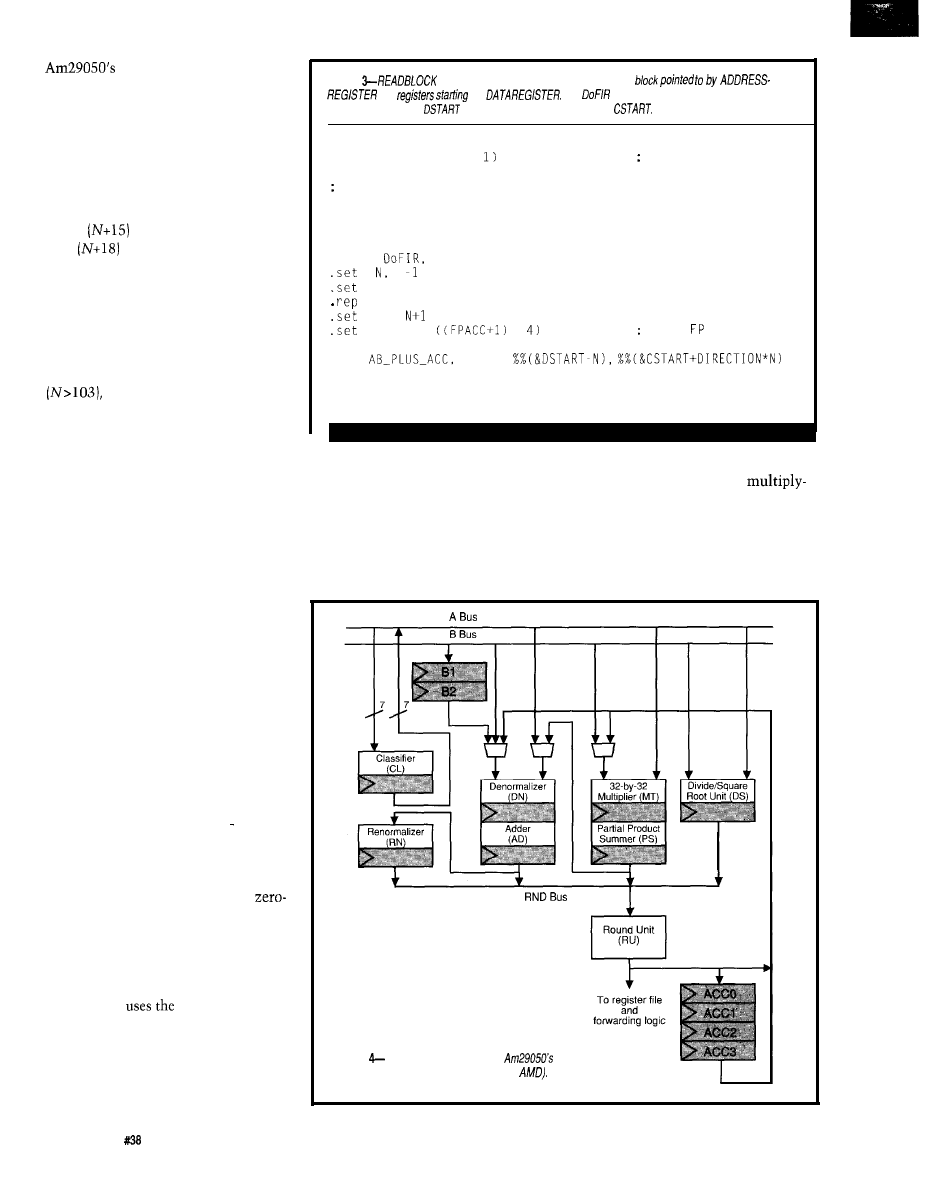
KEEPING THE FLOATING POINT
lies in the use of the FPU shown in
PIPELINE FULL
After modifying the code to take
advantage of on-board registers or
burst memory, you would expect the
filter speed to improve significantly,
but it doesn’t. The inefficiency now
Figure 4. The floating-point
and-accumulate FMAC instruction
makes use of the majority of the FPU
resources. Every FMAC instructions
takes 6 cycles. However, the pipeline
implies a new FMAC instruction can
Figure
Internal architecture of the
floating point unit (reproduced courtesy of
20
Issue
September 1993
The Computer Applications Journal

start (and complete) every 25 ns. I am
IF
not getting that kind of performance!
So where is the problem?
.endm
In checking the data books, I find
that although an FMAC instruction can
start every cycle, it cannot complete
until all data values are available.
Since four FMAC instructions all make
use of the single floating-point accu-
mulator at pipeline stage 3, they stall
at that point until the previous FMAC
instruction completes. This problem
means that each FMAC stalls for three
cycles before it proceeds. This hidden
inefficiency did not show up in the
original code. The memory accesses to
get data and coefficients were inter-
leaved with the FMAC operations so
each FMAC found its operands. Remov-
ing the memory accesses that occurred
in parallel with FPU operation exposed
this inefficiency.
The autoincrementing LOADM
instruction can’t be used to speed up
register loading with on-line circular
buffers because during the instruction,
no range checking would be per-
formed. Apparently the registers must
be loaded individually using the LO AD
instruction and the AD J ST macro
executed at every data fetch in the
loop. This is considerable overhead.
The Am29050 designers were
aware of this problem and provided
additional floating-point accumulators
to overcome stalls. Rewriting the code
to use all four accumulators fixes the
problem.
The memory management unit
and translation look ahead buffer,
(TLB), hardware can be programmed to
perform the pointer checking in
parallel with other instructions using
low overhead software tricks. A
circular buffer can be implemented by
using the virtual addressing mode
during the loop. The circular buffer is
obtained by mapping several virtual
addresses to a single physical address.
The memory management unit
can block memory pages from
to
so it’s possible to generate
The macro D
O
F I R, shown in
Listing 3, multiplies NUMB E R data
values stored at register DSTART with
the coefficients stored at register
CSTART. It takes all four accumulators
into account to calculate the partial
sum and the data values are stored at
the highest number’s register. The
variable D I R E C T I 0 N takes into
account the coefficients for filter tap
N-rissameasfortap
and READBLOCK macros can be used in
on- and off-line filters.
are our cross
compilers so inexpensive???
Because we
them away
free!
IMPLEMENTATION OF A
NO-OVERHEAD CIRCULAR
BUFFER ON A RISC CHIP
A fundamental deficiency on RISC
chips is the small number of address-
ing modes in the instruction set.
Implementing circular buffers would
appear to incur considerable overhead.
A simple array can be turned into
a circular buffer by using pointers and
pointer comparison. In simple pseudo-
code, the AD J US T macro used to adjust
the data block pointers becomes:
ADJUST, POINTER
POINTER++
dresses in modulos that are multiples
of 256 words. Note that my circular
buffer is 512 words. Only 193 locations
are used at any time.
Setting the TLB registers is
simple. They can be initialized by
masking the required virtual and
physical addresses. The macro
(shown in Listing 4) maps
the address V I RTUA L into the address
P H Y S I CAL and sets the TLB registers.
This macro does not turn on the
virtual addressing mode since it may
be invoked many times before all the
required TLB registers have been set
up. The new AD J US T macro needs no
error checking and becomes:
ADJUST, REGISTER
add REGISTER, REGISTER, 4
.endm
This approach to the circular
buffer means the real-time FIR code
looks like Listing and requires
1) instructions. This is a 400%
speed improvement over the first
implementation. I still have to use:
We base our cross compilers on the GNU C/C++ compiler from the
Free Software Foundation.
We provide you with one year of
support*, and give you a ready-to-run cross compiler with complete
for DOS, Windows, OS/2 2.0 or UNIX for $495 per year.
Or, get the extended support package for $895, which includes
GNU
and make, the CVS and RCS source code control
utilities,
and the
typesetting system.
Targets include i386,
Motorola 680x0,
and 88000, MIPS and
Hundred Acre Consulting
5301
Longley
Lane Suite D-l 44, Reno NV 89511
( 8 0 0 ) 2 4 5 2 8 8 5
The Computer Applications Journal
Issue
September 1993
21
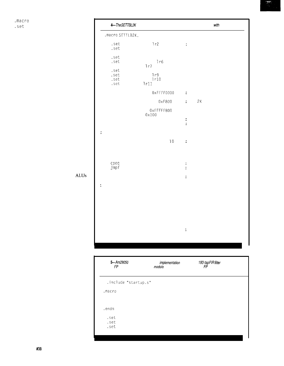
CHECKADJUST, REGISTER
CIRCBUFFTRAP,
CIRCBUFFERTRAPNUM
asleu
CIRCBUFFTRAP, REGISTER,
CIRCBUFFEREND
.endm
once each loop to ensure that the
pointers remain in the circular buffer,
but this is not significant overhead.
The ASLEU instruction performs the
pointer comparison in a single cycle. If
the R E G I ST E R address gets too high,
an
assert trap
is caused. The overhead
associated with this trap handling is
about seven cycles every 5 I2 times
through the loop. This is less than the
three cycles every loop for using a
compare (CPLEU), jump (JUMPT), and
delay slot combination of instructions.
EVALUATION OF THE AM29050
AS A CHIP FOR FIR OPERATION
The Am29050 has many features
found in DSP chips. The register stack
can be used for data and coefficient
storage. It has a separate instruction
bus so data and instruction fetches do
not compete. It has a number of
that operate in parallel, and the FPU
operates in a single cycle. An advan-
tage of the Am29050 is that it is a
RISC chip and the internal architec-
ture is exposed so I can maximize the
throughput of the pipelines.
What, then, is missing from the
Am29050 as a “perfect” DSP chip?
Several things come to mind from
examining the FIR algorithm.
The Am29050 has a limited
amount of on-board RAM memory
(192 registers); it is on the small side
when compared with the newer DSP
chips, but is still large enough to be
useful. The problem is reloadability,
being defined as the ability to reload
one part of the register file from
external memory while processing
using another part. Currently, while
floating-point operations are per-
formed, the external address and data
paths are inactive. If these paths could
be used in parallel, the speed would
increase. Since the Am29050 is a RISC
chip, developing complex instructions
for parallel operations goes against its
basic design. There is, however, one
important instruction where this
Listing
macro is used to implement 2K
circular buffer operations
zero overhead.
PHYSICAL, VIRTUAL
VTAGMASK,
set
registers
TLBLINEMASK, lr3
.set
RPNMASK, lr3
VE, lr5
PROTECTION,
.set
MMUPS,
TLBLINE, lr8
TLBWORDO,
TLBWORDl.
TEMP,
LCONST
VTAGMASK,
see manual for defins.
LCONST
TLBLINEMASK,
for pages operation
LCONST
RPNMASK.
LCONST
MMUPS,
LCONST
VE, 0x4000
valid entry bit
LCONST
PROTECTION, 0x380
supervisor mode
Find out which line in TLB registers are needed
and
TLBLINE, VIRTUAL, TLBLINEMASK
srl
TLBLINE, TLBLINE,
2K mode
; See if this TLB set 0 is already in use
mfsr
TEMP, TEMPLINE
and
TEMP, TEMP, VE
TEMP, TEMP, VE
is VE bit set?
.+oxc
skip to and
nop
add
TLBLINE, TLBLINE, 64
change to other set
Build the TLB words and move them in
and
TLBWORDO, VIRTUAL, VTAGMASK
or
TLBWORDO, TLBWORDO, VE
or
TLBWORDO, TLBWORDO, PROTECTION
mtsr
TLBLINE, TLBWORDO
add
TLBLINE, TLBLINE, 1
and
TLBWORDl, PHYSICAL, RPNMASK
mtsr
TLBLINE, TLBWORDl
mtsr
mmu, MMUPS
set
mmu page size
.endm
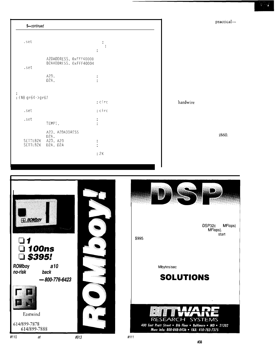
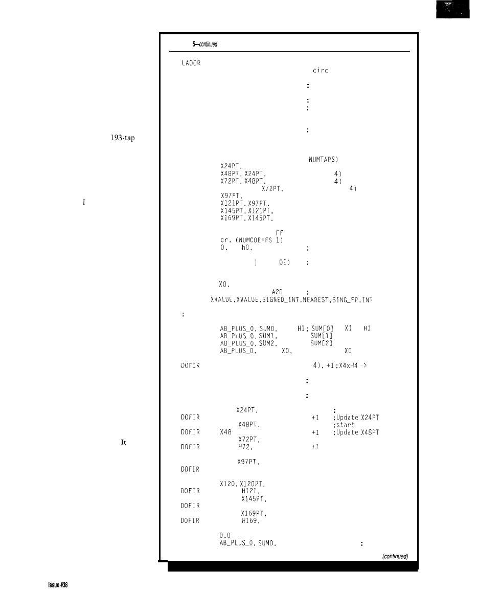
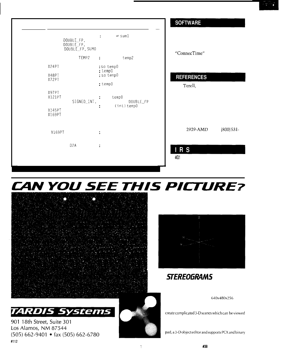
Listing
processor code for the
of a real-time
using data
cache, full pipeline coding, hardware
arithmetic, and simultaneous and integer operation
coding strategies.
ADJUST, REGISTER
NOTDEFINED
NUMTAPS, 193
NUMCOEFSS, 97
FILTERCOEFF, Ox18000
(continued)
22
Issue
September 1993
The Computer Applications Journal
Listing
.set
BUFFSIZE, 0x400
PHYSICALBUFFER, 0x19000 physical address
.set
CIRCULARBUFFER, 0xFF9000
virtual address
.set
CIRCBUFFERTRAPNUM, 65
user dependent
.set
.set
TEMP, gr83 code
.set
gr84
A/D address
.set
gr85
D/A address
.set
CIRCBUFFEREND, gr86
Set TLB for virtual address mapping
used as temps in use later)
.set
CIRCBUFFPT, gr64
buffer virtual addr
PHYSICALPT, gr65
buffer physical addr
TWOK, gr66
2K page
.set
gr67
used to set TRAP addr
LADDR
LADDR
DZAADDRESS
physical = virtual
physical = virtual
LCONST
TWOK, 0x800
blocks
LADDR
PHYSICALPT. PHYSICALBUFFER
(continued)
parallel operation appears
the load multiple (LOADM) instruction.
When I originally wrote this
article, I had the following suggestion:
If this had simply been a software
problem, then the programmer/
compiler would have been warned
about reading data before it was ready
and avoided the conflict. RISC chips
and the compiler are supposed to
interact for optimium code and
perhaps a version of the Am29050 chip
could be released for DSP users
without the data dependency between
the LOADM and the FP instructions
being
checked and simply
relied on the compiler/assembler to
check the data dependency.
However, since that time
I have
become older and wiser and have had
experience with a chip without the
hardware checks-the Intel
A
fast chip it might be, but to get that
maximum performance requires very
detailed knowledge of the chip
architecture because of the missing
interlocks. My attitude now is hard-
ware checks (scorecarding) are an
The BEST in ROM
emulation technology:
Mbit
includes
day,
money
guarantee!
Call Today
Grammar
Engine
Inc.
HARDWARE
Check out our complete line of DSP boards based on powerful
floating-point processors like the AT&T
(25
and the Analog Devices ADSP-21020 (75
Several
analog interface modules are available. DSP boards
at just
SOFTWARE
W e have everything you need to do DSP software
development, including C compilers, assemblers, source-level
debuggers, algorithm development tools, and many example
programs. Data can be transferred between the DSP board and
host at up to 3
with the host interface library (source
code included).
Call our friendly, knowledgeable staff to discuss your
applications and we’ll show you how easy it is to take
advantage of DSP technology.
800-848-0436
921
Dr., Suite 122
Westerville, OH 4308 1
Fax
See us
Embedded Systems Booth
The Computer Applications Journal
Issue
September 1993
23
essential feature of a processor as it
allows the programmer to get “excel-
lent” performance without becoming
intimate with the architecture.
Another problem is that currently,
to add the values of two floating-point
accumulators used in multiple FMAC
instructions, the register values must
be brought out of the FPU into local
registers (M FACC) and then added. The
lack of such an add instruction
increases the length of the
FIR
loop by about 3 cycles in 400, so it is
relatively unimportant. However, for
smaller DSP loops such as in the IIR or
FFT, it might be more relevant.
CONCLUSION
In this article examined the
application and theory behind the
implementation of high-speed FIR
filters on the Am29050. I also illus-
trated that the Am29050 processor had
many architectural features commonly
found in DSP chips.
One major DSP feature missing is
the ability to allow external block data
memory access to occur in parallel
with floating-point operations. This
would allow the on-board data cache
to be refilled from external memory
with minimum overhead.
In addition to being a high-speed
general-purpose processor, the
Am29050 is no slouch as a DSP chip.
Will I see this processor in industrial
DSP applications? The performance is
already there and the floating-point
operation allows for fast development
time. There is currently a problem
associated with power consumption
and chip cost. The newly released
Am29240, based on the same 29k
processor core as the Am29050, offers
some interesting possibilities. is an
integer chip, has on-board instruction
and data cache, and a single-cycle
pipelined hardware multiplier. I am
currently exploring using this chip for
spectral analysis.
q
Michael Smith is a professor of
Electrical and Computer Engineering
at the University of Calgary, Canada,
where he teaches courses on Com-
puter Graphics, Comparative Proces-
sor Architecture, and Systematic
Programming Techniques.
Listing
CIRCBUFFPT, CIRCULARBUFFER
SETTLBZK
PHYSICALPT, CIRCBUFFPT ;
buffer
SUB
TEMP, CIRCBUFFPT. TWOK
SETTLBPK PHYSICALPT, TEMP
block below
ADD
TEMP, CIRCBUFFPT. TWOK
SETTLBZK
PHYSICALPT, TEMP
block above
SUB
CIRCBUFFEREND, TEMP, 4 used in pointer checks
ADD
TEMP. TEMP, TWOK
SETTLBZK
PHYSICALPT, TEMP
second block above
SETASSERTTRAP CIRCBUFFERTRAPNUM, circbufftrap
LADDR
XOPT. (CIRCBUFFPT + 4 *
sub
XOPT, (DATABLOCKSIZE * 4)
sub
(DATABLOCKSIZE *
sub
(DATABLOCKSIZE *
sub
XCENTREPT,
(DATABLOCKSIZE *
sub
XCENTREPT, 4
sub
(DATABLOCKSIZE * 4)
sub
(DATABLOCKSIZE * 4)
sub
(DATABLOCKSIZE * 4)
LADDR
TEMP. FILTERCOE
mtsrim
loadm
0.
TEMP
mtsrim
cps, (PI SM
LOOP:
move in the filter coeffs.
turn on virtual data mode
READBLOCK
XOPT, DATABLOCKSIZE; load in data
load
0, 0, XVALUE,
get value from A/D
convert
Clear the accumulators and avoid blocking x0
fmac
Xl.
= x
fmac
X2, H2:
= X2 x H2
fmac
X3. H3:
= X3 x H3
fmac
SUM3,
HO: SUM131 = x HO
X4, H4, (DATABLOCKSIZE
X23, HZ3
store
0, 0, XVALUE, XOPT
moved fp store-don't block
ADJUST
XOPT
adjust buffer pt
READBLOCK X24.
DATABLOCKSIZE
get next block
x24
H24, DATABLOCKSIZE,
moved
READBLOCK X48
OATABLOCKSIZE
this
H48, DATABLOCKSIZE,
moved
READBLOCK X72
DATABLOCKSIZE
x72
DATABLOCKSIZE,
READBLOCK X97,
DATABLOCKSIZE
X97, H97, DATABLOCKSIZE, -1 ;coeffs symmetric
READBLOCK
DATABLOCKSIZE
X121,
DATABLOCKSIZE, -1
READBLOCK X145,
DATABLOCKSIZE
X145, H145, DATABLOCKSIZE, -1
READBLOCK X169,
DATABLOCKSIZE
X169,
DATABLOCKSIZE, -1
load
XCENTRE, XCENTREPT
fmac
XCENTRE, HCENTRE
centre tap
24
September1993
The Computer Applications Journal
Listing
5-continued
mfacc
TEMPl, DOUBLE-FP, SUM1 templ
mfacc
TEMPP,
SUM2
mfacc
TEMP3,
SUM3
mfacc
TEMPO,
dadd
ADJUST
dadd
ADJUST
ADJUST
dadd
ADJUST
ADJUST
convert
ADJUST
ADJUST
ADJUST
TEMPl, TEMPl.
templ +=
ready
TEMPO. TEMPO, TEMP3
+= temp3
ready
TEMPO, TEMPO, TEMPl
+= templ
get
ready
Yn, TEMPO,
NEAREST, INT,
yn =
XCENTREPT
; check and adjust the pointers for the circular buffer
CHECKADJUST
finish the convert
jmpfdec
COUNTER, LOOP
store
0, 0, Yn,
output Yn
circbufftrap:
CIRCBUFFTRAPHANDLER
Software for this article is avail-
able from the Circuit Cellar BBS
and on Software On Disk for this
issue. Please see the end of
in this issue for
downloading and ordering infor-
mation.
T.J.
Introduction to Digital
Filters, MacMillan Press, 1983.
Am29050 Microprocessors User’s
Manual, AMD, 1991.
For more information on the
Am29050 processor DSP library,
contact the AMD 29k hotline:
(800)
(U.S.],
5202 (Canada).
Very Useful
402 Moderately Useful
403 Not Useful
Why pay $30 to $50 for a 3-D Stereogram
at your local mall when you could
M A K E Y O U R O W N !
3-D
and
SOLID
OBJECT MODELING
System Requirements: DOS PC, 386-486
with
4.0
MB RAM, hard disk, SVCA
color
mode.
This full 3-D object modeling code allows you to
from anyperspectiveordistance,andthen rendered
into your own random-dotstereogram image.
Thesystem is mouse-driven,containsa basicsketch
file output.
The
Computer Applications
Journal
Issue
September 1993
2 5
Using Your
PC for
Function
Analysis
and Control
David S. Birkett
omputer-based
instrumentation is
becoming more and
more common. A
diverse new breed of instruments that
have varying levels of computer
control are starting to appear in the
marketplace. On one hand, there are
the software-based simulations of
“hardware experiments.” These
“software labs” give you the ability to
experiment with and observe the
operation of experimental circuits
without having to actually wire up real
components on breadboards. On the
other hand, there is a wide range of
computer-controlled versions of the
traditional mix of bench gear. At this
end of the spectrum are devices like
computer-based logic analyzers, power
supplies, frequency counters, oscillo-
scopes, and so forth. A related trend is
to embed more intelligence into test
equipment and provide it with a
command interface so it can be
controlled by, or send data to, a
separate computer system. These
trends will continue and, in all
likelihood, will change the nature of
testing and test equipment. This will
lead to new methods of circuit design
and testing.
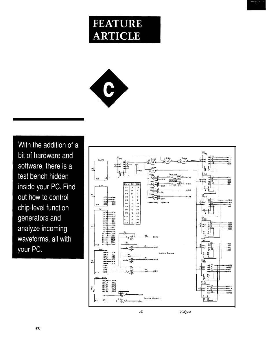
I have coupled my PC with a
simple hardware/software system, and
Figure l--Based on an
off-the-she/f PC expansion card, the function
adds the basics necessary for
measuring and controlling real-world signals.
26
Issue
September 1993
The Computer Applications Journal
in doing so, I have created an
instrument that has great
C O U N T
2219500
R E S O L U T I O N - 6 4
potential in laboratory
G A T E ( S E C S ) 2
control and measurement
8
F R E Q
1110085
applications. I call this new
STABILITY
-47
instrument a
function
ADO
4.358108
analyzer. In essence, it allows
AD1
7.030303
any voltage-controlled
A D 2
4.98646
AD3
4.967082
oscillator (VCO) to be
controlled by keyboard. Now
READ COUNT AGAIN? (Y/N) Y
I
can control a variety of
inexpensive IC-based signal
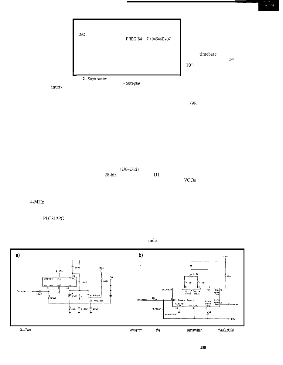
Figure
listing (item 6) includes channel number, raw count,
sources. This control
gate
period and resolution, frequency
period, frequency
l
64 (for
use
with prescaled channel),
frequency stability with respect to previous reading,
face transforms them into
and four analog voltages.
precise, versatile frequency
synthesizers. I gave the function
analyzer its name because it operates
on mathematical principles. It uses an
IBM-compatible PC equipped with a
multifunction I/O card that has been
enhanced with an elementary counter.
HARDWARE
Figure 1 shows the schematic of
the computer interface and some of
the external hardware that is required
by the function analyzer. Notice that
there are five ports available on the
multifunction I/O card. This interface
provides the user with 16 digital
inputs, 16 digital outputs, 16 analog
inputs, 2 analog outputs, and a
programmable pacer derived by
dividing a
crystal.
I created the function analyzer by
designing a circuit that could attach to
the PC through a
card from
B&C Microsystems. I decided to do
this because this interface card is
easily installed and, through its driver
and utilities, offers a programmable
pendently cyclical operation
of the hardware and software
makes implementing a variety
of counter-based experiments
simple, flexible, and reliable.
The system is equipped with a
quartz
and boasts a
resolution of 1 part in
(1 in
Its gate is continuously
adjustable from the keyboard,
and gate times can vary from
0.1 second to several minutes.
It has four input channels, and
channel selection is also
selectable from the keyboard.
interface that can be enhanced for just
about any purpose. Another reason I
chose to work with this card is that its
hardware interface is well documented
and it also includes a fair set of sample
programs written in BASIC that
illustrate how to take advantage of
various facets of the card. You can use
this information, like I did, to come up
with a wide variety of custom I/O
applications.
The CA3
prescaler chips give the
counter a wide frequency range. This
range extends from a few hertz at the
low end to gigahertz at the top end of
the range. These frequency measure-
ments are available for processing and
display by the PC.
In my application, seven 4-bit
binary counters
are used to
make a
frequency counter.
and U2 cyclically gate, freeze, and
reset the counter chain at a rate that is
set by the programmable pacer. The
counter software, shown in Listing
I
,
continuously reads 16 digital and 12
analog inputs. These readings are used
to recognize when a valid frozen count
has occurred which, in turn, is used to
compute a frequency referenced to the
gives the function analyzer’s voltage
pacer crystal.
readings a certain degree of absolute
The design of this counter makes
accuracy and makes implementation
the system very versatile. The
of the signal buffers trivial. This
Figure 2 shows the PC’s output
from a single reading. The data
represented by Figure 2, in addition to
frequency information, presents
simultaneous measurements from the
analog portion of the circuit. These are
used to monitor analog outputs that
control
or to record other
corollary voltages. All of the analog
lines are buffered by operational
amplifiers in order to protect the I/O
card. As is usual in PC-based instru-
mentation, the analog inputs are
calibrated in software against external
voltage standards. Software calibration
Figure
examples of function generator chips that can be controlled by the function
include a) BA 1404 stereo FM
chip and b)
precision waveform generator.
The Computer Applications Journal
Issue
September 1993
2 7
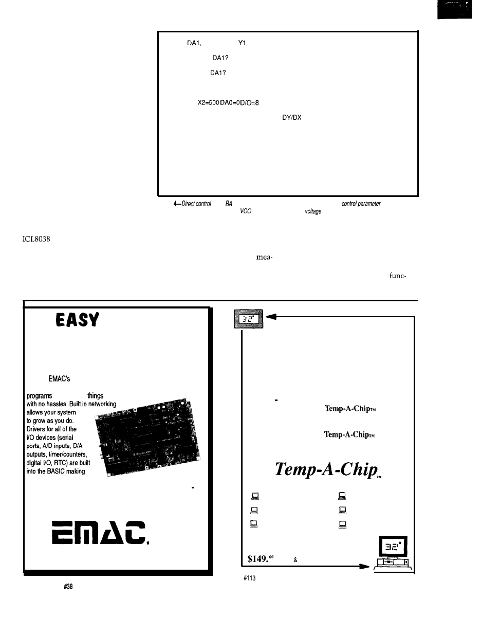
accuracy is assured as long as the
buffers are stable and linear. The gain
of the individual buffers may be set in
accordance with your specific hard-
ware considerations.
FREQUENCY SYNTHESIS
ENTER INCREMENT? 300
Figure 2 may be considered an
example of “direct” operation of the
function analyzer. In direct operation,
a control parameter is used to set an
analog voltage level, which is then
applied to a VCO. Next, various
calibrated frequency and voltage
measurements are recorded. These
show the system’s response to the
settings of the control parameter.
Figure 3a shows a BA1404 FM trans-
mitter chip which is tuned with an
external varactor to operate at approxi-
mately 60 MHz (Figure 3b shows
another potential application using an
waveform generator chip).
Software can be easily written which
will step the voltage applied to the
varactor through a range of values, and
thereby change the frequency of the
chip. The table in Figure 4 lists a
Xl = 500
DA
FREQ.
A D
AD
ACC STAB MAG
T E S T
2200.0
58204610.0
2.67
4.30
0.00 44
-14 0
0.0000
2500.0
60895620.0
3.03
4.89
0.00 43
-14 0
0.0000
2800.0
64898110.0
3.39
5.47
0.00 43
-12 0
0.0000
3100.0
67698180.0
3.75
6.06
0.00 43
-14 0
0.0000
3400.0
69847040.0
4.12
6.65
0.00 43
-15 0
0.0000
3700.0
71594880.0
4.48
7.23
0.00 42
-17 0
0.0000
4000.0
73068800.0
4.84
7.81
0.00 42
-17 0
0.0000
FREQ CHANNEL=
8
Figure
of the 1404 via external varactor tuning. The PC DAC
is stepped from
2200 to 4000
in seven steps and the
frequency and varactor
are measured.
sequence of D/A settings (this is the
control parameter in this experiment
and its settings are shown in column
1). You can read the frequency
sured by the counter during each step
by looking at column 2. Column 3
lists the varactor’s actual control
STEP
ESTABLISH
THE CALIBRATION MATRIX
ENTER FIRST
2200
ENTER LAST
4000
voltage as measured by a calibrated
ADC. The measurements of Figure 4
completely describe the operation of
the VCO over a range of interest.
Figure 4 shows that the frequency
and voltage of this system are
tions of the control parameter. These
TO USE
SINGLE BOARD COMPUTERS
With EMAC’s feature packed Single Board Computers and easy to
use BASIC compiler your application/product can become a reality in
no time.
BASIC compiler can process real time interrupts from
a number of sources easily and efficiently. Multitasking allows your
to do several
all at the same time
themextremelyeasytouse.
If BASIC is not your
language of choice, EMAC offers Assembler, ANSI C, and Forth
you
choose. So take one of our single boards computers for a 30 day risk
free test drive and just see what it can do for you! EMAC’s single
board computers start at $249.00 for the EPAC 3000 shown above.
inc.
618-529-4525
FAX: 618-457-0110
P.O.BOX 2042 CARBONDALE, IL 62902
DO YOU NEED CONTROL ?
If you’re looking for a temperature sensor that
allows your computer to not only monitor the
temperature but respond to it,
look no further.
Temp-A-Chip,, is a solid state temperature
sensor providing truly linear measurement of
temperature. The
is an
intelligent, user configurable sensor which
interfaces with your computer. No batteries are
needed to operate the
,
it plugs
into any standard RS232 interface.
LCD Display
Solid State Design
No Batteries Req’d
RS-232 Interface
Easy To Install
Easy To Use
Can You Afford Not to Call Today?
$5.00 P H
(800) 274-8699
28
Issue September
1993
The Computer Applications Journal
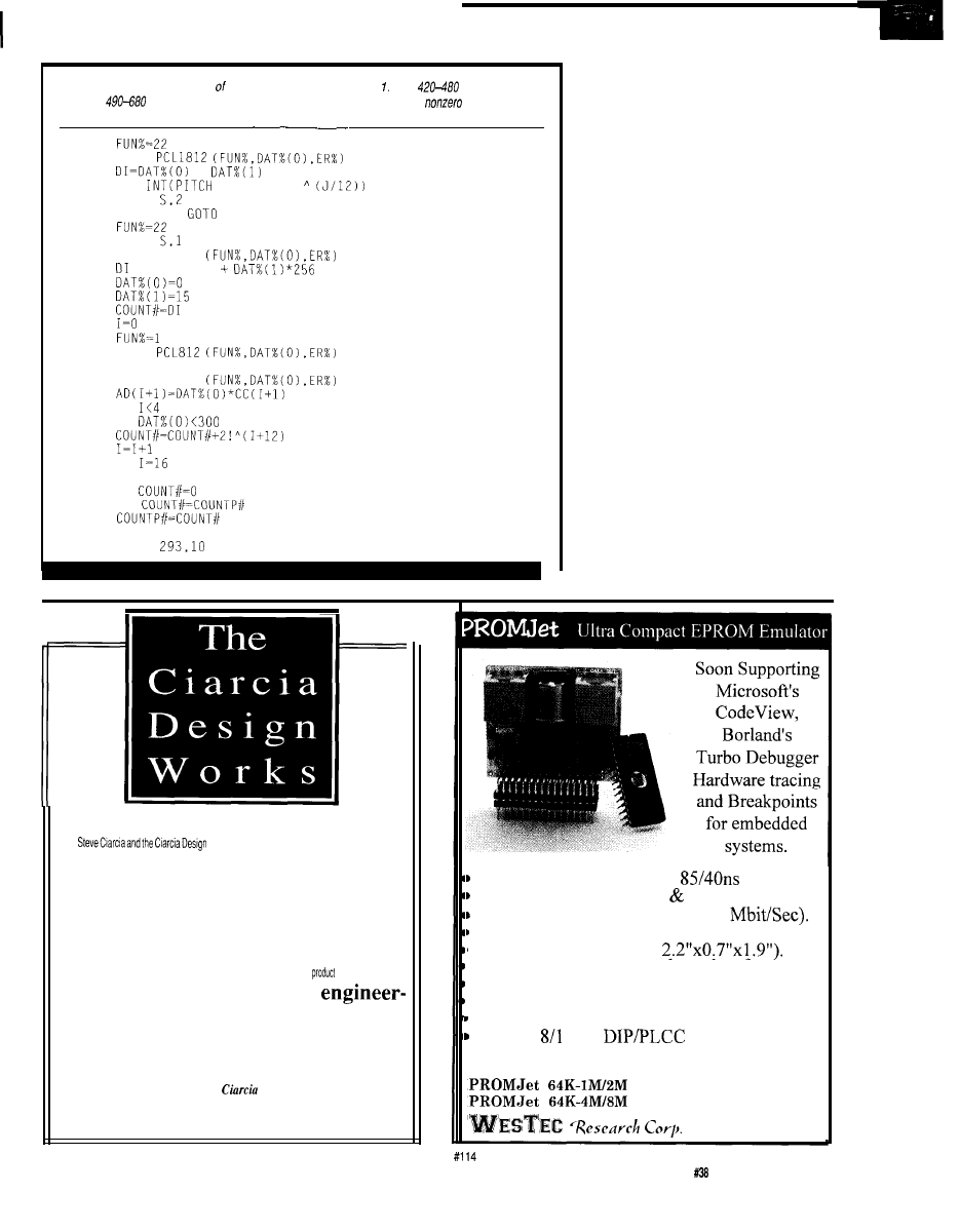
Listing
l-Software for acquisition data from counter chain of Figure Lines
provide initializa-
tion, lines
repeated/y read the counter, and line 690 recognizes a frozen
count and jumps to
the end of the program.
420
4 3 0
CALL
440
+
* 256
460
S =
* MUTE * 2
470
SOUND
480
IF DI<>O
420
490
500
SOUND
510
CALL PCL812
520
= DATA%(O)
530
540
550
560
570
580
CALL
590
FUN%=3
600
CALL PCL812
610
620
IF
GOT0 650
630
IF
GOT0 650
640
650
660
IF
GOT0 680
670
GOT0 590
680
IF
GOT0 490
690
IF
GOT0 720
700
710
GOT0 490
720
SOUND
functions are locally monotonic. Since
the step size may be refined without
limit, the accuracy of the functions is
limited only by the stability of the
VCO and the resolution of the instru-
ment. It is easy to approximate
(through programmatic computation)
the inverse of these functions. From
the example shown in Figure 4, the
control parameter (column 1) would
become a function of the applied
voltage or of the frequency counted by
the system. A simple linear interpola-
tion on data accomplishes this, with
accuracy improving as the step delta
decreases. It is this capability of
precise functional inversion that is the
basis of the operation of the function
analyzer in its most powerful mode:
the indirect mode.
Compare the direct data shown in
Figure 4 with that listed in Figure 5,
which illustrates data acquired using
the indirect mode. In Figure 5, the
VCO steps from 60 MHz to 70 MHz in
1 -MHz intervals. For each step, the
instrument estimates, using the direct
data of Figure 4, the control parameter
Does your big-company marketing
Worksstaff mayhavethesolution.
department come up with more ideas
Wehaveateamofaccomplishedprogrammersandengineersreadyto
than the engineering department can
design products or solve tricky engineering problems. Whether you
cope with? Are you a small company
need an on-line solution for a unique problem, a
for
a startup
that can’t afford a full-time
venture, or just experienced consulting, the Ciarcia Design Works is
ing staff for once-in-a-while designs?
readytoworkwith you. Just fax me your problem
andwe'llbeintouch.
Remember...a
design works!
Call (203) 8752199 Fax (203) 871-8986
Emulates 64 Kbit to 8 Mbit
EPROMs.
Accepts Binary, Ext. Intel Motorola formats.
Fast download from printer port (1
Fits into EPROM socket to minimize noises.
Double sided SMT (size:
Jumperless configuration through software.
Ni-Cd battery backup. Power-up emulation.
Cascadable to 128 bits. Generates RESET+/-.
Comes complete with software and cables.
Optional
6 bit
adapters.
15 DAY MONEY-BACK GUARANTEE.
85ns
$1951295
85ns
$4951695
(2 13) 664-8909
The Computer Applications Journal
Issue
September 1993
29
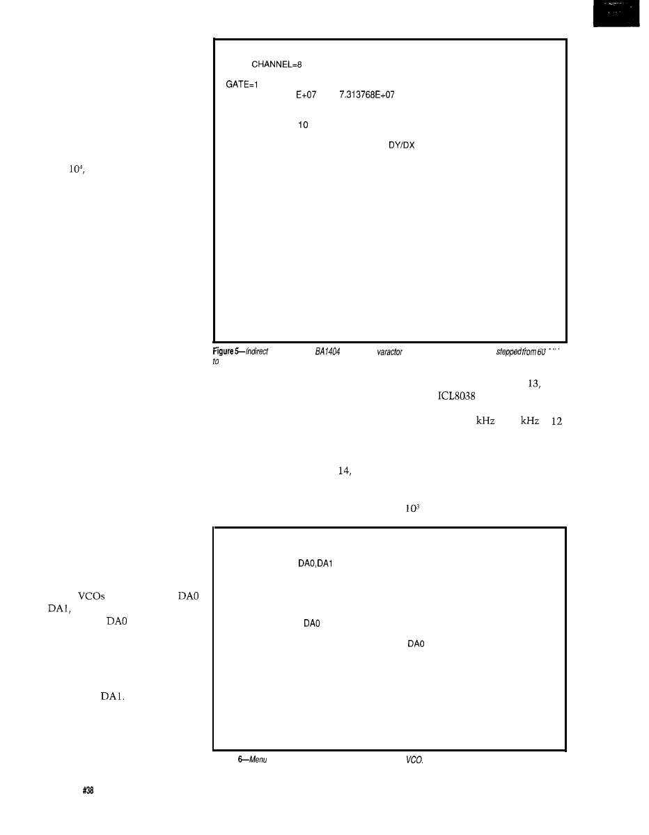
required to hit the target frequency
[column 9). Once it is computed, the
control parameter is applied and the
resulting frequency is measured
(column 2). Column 6 of Figure 5 is
devoted to a logarithmic measure of
the error between the desired fre-
quency of each step and the actual
measured frequency. This column
indicates an average error of less than
1
part in
or a few kilohertz, for
control of the 60-MHz oscillator. This
accuracy will improve if the data in
Figure 4 has a finer resolution between
adjacent steps. Figure 5 documents the
operation of the function analyzer as a
frequency synthesizer in which a VCO
is brought under precise numerical
control.
OPERATION
It is important to note that
calibration data like that shown in
Figure 4 can be generated in seconds
for any stable VCO. Once this data is
measured and captured, the inexpen-
sive VCO has become a versatile
frequency synthesizer and can be
considered a “calibrated” test instru-
ment. The capabilities of this elemen-
tary piece of hardware can then be
maximized by using menu-driven
software.
Figure 6 shows a menu that has a
variety of useful keyboard operations
for control and measurement of a
VCO. The first seven items enable the
operator to set the period of the
counter gate, set the output level of
any of the D/A converters, select a
frequency channel, read the analog
channels, read a count or frequency,
and calibrate the ADC channels. Items
8 and 9 are the basic calibration
sweeps for
under control of
and
respectively. Item 8 provides
linear stepping of
while reading
the counter with double precision. It
will also read and record the analog
channels. Item 9 dispenses with
double precision, but allows 100
samples to be acquired for calibration
under control of
After calibration of a test oscilla-
tor using items 8 or 9, indirect opera-
tion follows using item 10 or 11,
respectively. With item 11, the
frequency may be stepped using a
STEP OUTPUT VARIABLE WITH DA1
FREQ
OUTPUT VARIABLE NUMBER 4
LIMITS 5.637421
ENTER FIRST VALUE? 60000000
ENTER LAST VALUE? 70000000
ENTER # STEPS?
DA
FREQ.
AD AD
ACC
STAB
MAG
TEST
2386.1
59982400.0
2.89
2.89
0.00
-36
0
0
60.0000
2480.7
60956230.0
3.01
3.01
8.38
-32
-18
0
61 .OOOO
2553.8
61993280.0
3.09
3.09
12.59
-40
-18
0
62.0000
2624.6
63021890.0
3.18
3.18
11.18
-35
-18
0
63.0000
2700.7
63998080.0
3.27
3.27
10.61
-46
-19
0
64.0000
2788.4
64996930.0
3.38
3.38
9.37
-44
-19
0
65.0000
2886.5
66004030.0
3.50
3.50
8.66
-43
-19
0
66.0000
2995.6
67000510.0
3.64
3.64
7.09
-52
-19
0
67.0000
3118.1
67998020.0
3.77
3.77
7.35
-46
-19
0
68.0000
3254.3
68997760.0
3.94
3.94
6.07
-45
-19
0
69.0000
3405.1
69994880.0
4.12
4.12
5.42
-42
-19
0
70.0000
STATISTICS
MEAN
2835.8 644994910.0
SIGMA
313.3
3168230.0
3.44
3.44
7.88
-42
-17
0
65.0000
0.38
0.38
3.25 6
5
0
3.1623
control of
fhe
via external
tuning. The target frequency is
MH
Z
70
MHz in 10 steps.
linear delta up to 250 times. Frequency
7 shows the operation of item
in
and four separate voltages are recorded
which an
audio oscillator
during each of these steps. Items 13
(Figure 3b) is swept chromatically over
and 14 are identical to item 11, except
the octave from 5
to 10
in
that no frequency measurement is
half tones. Note that the frequencies
made during each step. This drastically
displayed are the target since they
accelerates the speed of a sweep. A
aren’t measured. This frequency can
linear sweep is used for item and a
be verified, however, by operation of
logarithmic sweep for item 13. These
item 11 over the same band. This
two routines can collect up to 250
would show that an accuracy of 1 part
points in less than ten seconds. Figure
in
can be obtained for audio
STEP OUTPUT VARIABLE AGAIN? (Y/N) N
(1) SET PACER
(2) SET
(3) SET FREQUENCY CHANNEL (D/O)
(4) READ D/I
(5) READ A/D
(6) READ COUNT
(7) CALIBRATE A/D
(8) STEP
(DOUBLE PRECISION)
(9) STEP DA1
(10) STEP OUTPUT VARIABLE WITH
(DOUBLE PRECISION)
(11) STEP OUTPUT VARIABLE WITH DA1
(12) SELECT OUTPUT VARIABLES
(13) SWEEP OUTPUT VARIABLES WITH DA1 (NO FREQ MEASUREMENT)
(14) STEP OUTPUT VARIABLES WITH DA1 (NO FREQ MEASUREMENT)
(15) DISPLAY GRAPH
(16) SET PARAMETERS
(17) WRITE FILE DATA0
(18) WRITE FILE DATA1
(20) EXIT
Figure
for keyboard control-direct and indirect-of a
30
Issue
September 1993
The Computer Applications Journal
LIMITS
15938.17
4557.077
X1=1118
X2=1118
D/O=2
DA
FREQ.
A D
A D
A C C
STAB
M A G
TEST
3882.1
5000.0
7.57
7.57
-0.00
-1
-1
0
1.0000
3802.9
5297.3
7.42
7.42
0.00
-1
-17
0
2.0000
3719.0
5612.3
7.26
7.26
0.00
-2
-18
0
3.0000
3630.1
5946.0
7.09
7.09
0.00
-2
-18
0
4.0000
3537.0
6299.6
6.90
6.90
0.00
-3
-18
0
5.0000
343808
6674.2
6.71
6.71
0.00
-4
-18
0
6.0000
3334.0
7071.1
6.50
6.50
0.00
-4
-18
0
7.0000
3222.3
7491.5
6.29
6.29
0.00
-5
-18
0
8.0000
3106.6
7937.0
6.07
6.07
0.00
-6
-18
0
9.0000
2984.1
8409.0
5.82
5.82
0.00
-8
-19
0
10.0000
2851.0
8909.0
5.57
5.57
0.00
-10
-18
0
11.0000
2710.4
9438.7
5.28
5.28
0.00
-13
-18
0
12.0000
2560.8
10000.0
5.00
5.00
0.00
-33
-19
0
13.0000
STATISTICS
M E A N
3290.7
7237.4
6.42
SIGMA
410.5
1556.7
0.80
Figure
control
(chromatic scale).
6.42
-0.00
-7
-17
0
7.0000
0.80
0.00
8
5
0
3.7417
frequencies synthesized in this
manner.
The PC brings to bear substantial
processing and other capabilities
which enhance the utility of the
function analyzer beyond mere
acquisition and display of calibrated
measurements. For example, column 6
in Figure 5 gives a logarithmic mea-
sure of the accuracy with which one
variable approximates another. The
variables to be compared (usually the
target and measured frequencies] are
selected by menu. Column 7 in Figures
and compares consecutive values
of any selected variable; if this variable
is supposed to be constant, the column
measures its stability in parts per unit.
As shown in Figures 5 and 7, after
every sweep in indirect mode each
column is processed for mean and
standard deviation. Suppose, for
example, that after an initial calibra-
tion routine, a VCO is measured via
item
11
at a fixed frequency 100
consecutive times. Then the sigma
value of column 2 is an excellent
measure of the frequency stability of
this VCO. This sophisticated and
The Computer Applications Journal
3 1
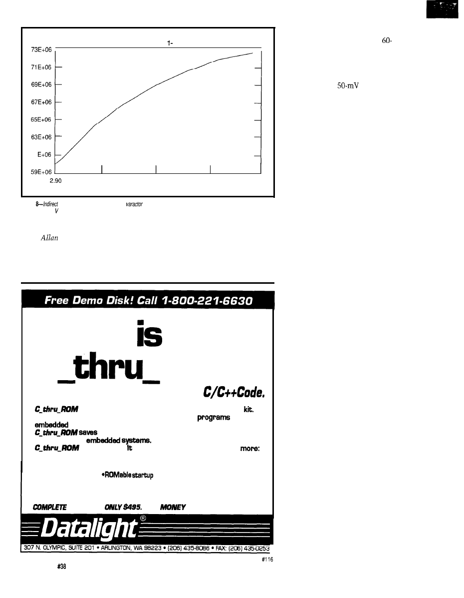
61
-DATA
3.40
3.90
4.40
4.90
Figure
control
of BA 1404.
Here, the
voltage, as
measured
by the calibrated ADC channel, is
stepped in 50-m increments.
formerly tedious measurement (known
see, however, that any variable may
as the
variance)
is performed
play the role of frequency. This
automatically.
flexibility means that in a complex
In all examples so far, we have
circuit, virtually any two variables
illustrated the control of frequency in
which vary with one another can be
direct and indirect mode. It is easy to
plotted, one as a function of the other.
What
C
ROM?
ROM Your Borland or Microsoft
is the complete ROM development software tool
It lets you run Microsoft and
Borland C and C++
on an
80x88 CPU without
using DOS or a
BIOS.
you money. There are no DOS or BIOS royalties
to pay for
your
is complete!
indudaa the following and much
*Supports Borland’s Turbo Debugger.
*Remote Code View style source level debugger.
code brings CPU up from cold boot.
l
ROMable library in source code.
*Flexible 80x88 Locator.
PACKAGE
3-Y
BACK GUARANTEE.
This idea is illustrated in Figure 8,
which shows the operation of a
MHz oscillator. In this case, the
varactor voltage is a function of the
control parameter. The control voltage
is produced by the function analyzer
and is stepped in
increments.
This experiment shows the frequency
of the oscillator (displayed in this
figure) as a function of the stepped
varactor voltage.
Figure 9 shows a menu from one
of the programs
I
wrote as part of the
function analyzer. This program
facilitates the construction of a wide
variety of interesting variables after
data acquisition. For instance, the
current through a resistor may be
computed using selection 19. In this
case, A and B are a pair of calibrated
voltage readings that were taken at the
terminals of the load, and C is the
resistance of the load. For another
example, selection 16 computes a
derivative as a quotient of differentials,
where the differentials may be those of
any two selected variables. These are
but two examples of the postprocess-
ing capabilities provided by this
utility. Careful examination of the
menu in Figure 9 can give you an idea
of the program’s other features.
Limited only by the constraints of
monotonicity and stability, the
function analyzer can plot any of these
variables as a function of any other.
CONCLUSION
During this article, I have empha-
sized the measurement and control of
frequency. I did this to show you
examples of the primary use of the
function analyzer. Now that you see
the scope and sophistication of the
measurements that can be made with
the function analyzer, I hope you have
as much fun applying it as I did
designing it. PCs can produce musical
notes. It is easy to program the
instrument so that it “sings along”
with itself as it hits various frequen-
cies in indirect mode. The full utiliza-
tion of the PC will change the nature
of electronic test equipment.
q
David Birkett is currently writing a
book on mathematics, personal
computers and electronics.
32
Issue
September 1993
The Computer Applications Journal
STEP WHICH OUTPUT VARIABLE?
(2) COUNT
(3) FREQ
(4)
(6) AD(t)
(7) AD(2)
AD(3)
(9) AD(4)
IO) TARGET
INDEX
CONSTANT
13) 0
ACCURACY
‘8) STABILITY
9) (A-B)/C
MAGNITUDE
ENTER SELECTION?4
ENTER DY VALUE?4
ENTER DX VALUE?6
ENTER FIRST ACCURACY VARIABLE4
ENTER SECOND ACCURACY VARIABLE10
ENTER STABILITY VARIABLE4
INTER A VARIABLE
B VARIABLE
C VARIABLE
CONSTANT
WHICH FREQ4
WHICH AD FIRST6
WHICH AD SECOND7
WHICH TEST VARIABLE1 1
‘AKE WHICH MAGNITUDE
VARIABLES
VARIABLE?
BY
VARIABLE?
BY
Figure 9-Menu for construction
of useful variables
from primary acquired
any
variable may be
as a function of any other
variable subjected indirect control.
Software for this article is avail-
able from the Circuit Cellar BBS
and on Software On Disk for this
issue. Please see the end of
in this issue for
downloading and ordering infor-
mation.
B&C Microsystems, Inc.
750 North
Ave.
Sunnyvale, CA 94086
(408) 730-5511
Fax: (408) 730-5521
404 Very Useful
405 Moderately Useful
406 Not Useful
PAL
GAL
EPROM
EEPROM
FLASH
MICRO
XC1 736
PSD
5ns
Free software updates on BBS
Powerful menu driven software
. up to 128 Channels
up
to 400 MHz
Samples/Channel
Variable Threshold Levels
8 External Clocks
16 Level Triggering
Pattern Generator Option
LA12100 (100 MHz,24 Ch)
LA32200 (200 MHz,32 Ch)
LA32400 (400 MHz,32 Ch)
Price is Complete
Pods and Software
$2750 LA64400 (400 MHz,64 Ch)
included
Software
200
Sampling Rate
2 Analog Channels (2ch. Digital
8 Digital Channels (8ch. Logic Analyzer)
125 MHz Single Shot Bandwidth
4K Samples/Channel (Analog Digital)
808-8990
Link Computer Graphics, Inc.
3 6 9 P a s s a i c A v e , S u i t e 1 0 0 , F a i r f i e l d , N J 0 7 0 0 4 f a x : 8 0 8 - 8 7 8 6
The Computer Applications Journal
Issue
September 1993
3 3
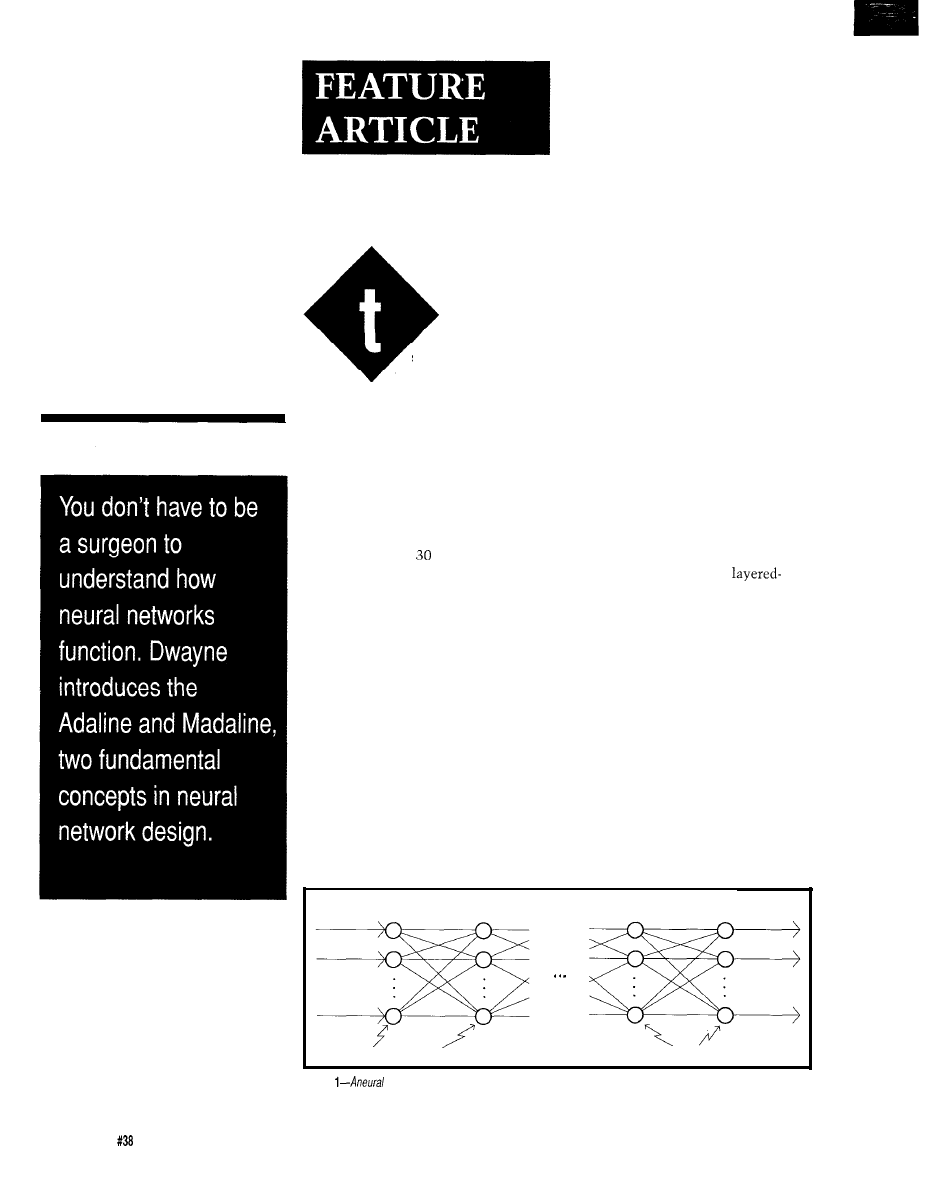
Neural
Network
Basics
Dwayne Phillips
he field of
neural networks
supports an approach
to solving difficult
problems using many small, simple
processors working in parallel. Neural
networks may seem like they are the
stuff of science fiction, but they are
reality; even better, they are simple to
implement.
Neural networks are more popular
now than in the recent past, but they
are certainly not new. They were first
discussed around years ago
(see
the
reference list at the end of this article),
and they were used to read characters
and predict the weather long before we
had megabytes of RAM and
supercomputers.
I’ll take you back to the beginning
with a brief review of the basics of
neural networks. Then I’ll look at
what they can do and teach you about
their basic building blocks and how to
implement them using simple C code,
FUNDAMENTAL CONCEPTS:
RECOGNIZING PATTERNS AND
THE HUMAN BRAIN
Neural networks are especially
adept at solving problems of pattern
recognition. There are many problems
that are trivial for people to solve but
confound traditional computer
approaches. Examples of these kinds of
problems are interpreting images (“see
Dick, see Jane, see Dick run”), predict-
ing weather (“red sky at morning,
bring a rain coat”), and reading
handwritten characters (except those
appalling scrawls by doctors). Conven-
tional approaches to these problems
require supercomputers and teams of
expert programmers.
Since people could solve these
pattern recognition problems easily,
researchers studied the structure of the
human brain. In the human brain there
are many processing elements called
neurons.
Each neuron is connected to
many of its neighbors through connec-
tions called synapses.
The researchers used this model to
develop neural networks. Figure 1
shows a diagram of a generic neural
network. The neural network takes
inputs on the left and produces
outputs on the right. In the middle are
several layers of processing elements
connected together with a
mesh network. Each processing
element is small, simple, and not very
powerful by itself. The power comes
from the combined effect of many
processing elements because of the
way that they all work together in
parallel on the “problem.”
Neural networks “learn” to
recognize patterns. This capability is
what makes them unique and also
contributes to their mystique. In order
for a neural network to learn, you
must supply the neural network with a
set of training data. This training data
should be typical of the problem under
consideration and should contain
Inputs
Processing Elements
outputs
Connections
Figure
network consists
of inputs
and outputs. The middle layer in the neural network is where learning
to recognize patterns occurs,
3 6
Issue
September 1993
The Computer Applications Journal
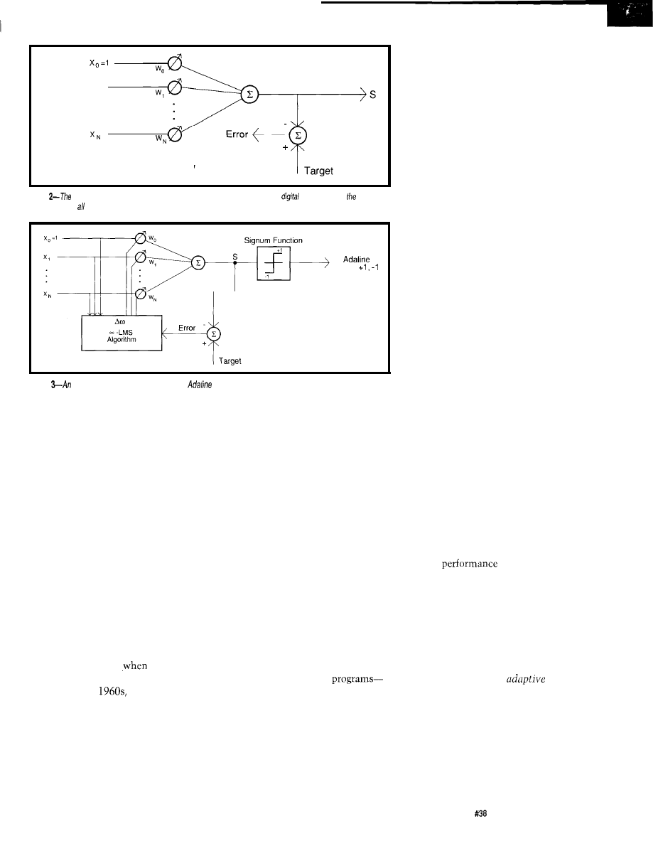
Input x,
Vector X
Weight
Vector W
Figure
Adaptive
Linear combiner is analogous to the
AND statement in
computers. It is basic
building
block of neural networks.
output
Figure
elementary neural network known as
distinguishes patterns that are linearly separable.
results that are known to be correct
answers. You begin by feeding one set
of training data into the neural
network and then examining the
output. If the output is wrong, you
adjust the synaptic weights of the
connections in the neural network.
You repeat this process of feeding data
into the network, examining the
output, and adjusting the weights until
the neural network’s output matches
the known correct answer. This is
called supervised learning. When the
learning (or training) is complete, you
store the adjusted weights. These
weights contain the “knowledge” that
will allow the neural network to
recognize patterns that were not in the
training data. The skill in manipulat-
ing neural networks is related to the
level of skill you use
you adjust
the synaptic weights.
During the
neural networks
were built using discrete hardware
components. The processing elements
consisted of simple voltage adders, and
the connections between the elements
were made through a type of variable
resistor. Researchers fed problems to
these systems, and feedback loops
were employed to adjust the resistors
until the neural network matched the
correct answers. With time, all things
progress. Now, you can buy neural
network chips that are electrically
alterable. What makes these devices
particularly useful is that after you
train them, they will store the weights
that produce correct answers.
Another method in wide use today
is to simulate neural networks in
software on traditional computers. The
simulation is a program that imple-
ments neural network equations like
those I’ll show you a little later. As the
code segments given below will
demonstrate, these programs are
simple and typically involve array
multiplication and addition.
These neural network simulation
programs have one great advantage
over traditional computer
they are extremely adaptable. Since
neural networks can learn (and can be
retrained), you write a neural network
program once, then retrain it to teach
it how to solve new problems. Tradi-
tional computer programs are algorith-
mic-meaning you code the algorithm
in a programming language. The
algorithm, however, is different for
each problem, so you must write a
new program for each new problem.
Neural network programs are adap-
tive-you write the neural network
program once, and adapt it by storing
different sets of weights that solve
different problems.
THE THREE STEPS IN USING A
NEURAL NETWORK
There are three steps in using a
neural network input data, train the
network, and use the network on new
problems. The first step could take the
longest depending on the method you
use to input the data. Neural networks
can only work with numerical data. If
you have any textual data you want to
use, you must first transform it to
numbers. Your neural network
program may query a user for input
data, or you may write routines to read
data from database or spreadsheet files.
Training is the process of running
the training data through the neural
network and adjusting the network
until its output matches known
correct answers. The training data
must have known correct answers.
The neural network adapts itself, or
learns, during the training phase. The
algorithm the neural network uses to
adapt itself is called the learning law.
To process new cases, you input
new data into the neural network and
wait for the answer. If the data for the
new cases are similar to the training
data, then the neural network will
produce correct answers. The key to
accurate
is the training
data. You need many representative
sets of data for training. How many
samples you will need, and how
representative they must be, is open
for experiment.
THE ADAPTIVE LINEAR
COMBINER
Figure 2 shows an
linear
combiner. The adaptive linear com-
biner is the basic building block of all
neural networks. It is to neural
networks what the AND gate is to
digital computers. The adaptive linear
combiner multiplies each element of
an input vector by corresponding
elements of a weight vector and
The Computer Applications Journal
Issue
September 1993
3 7
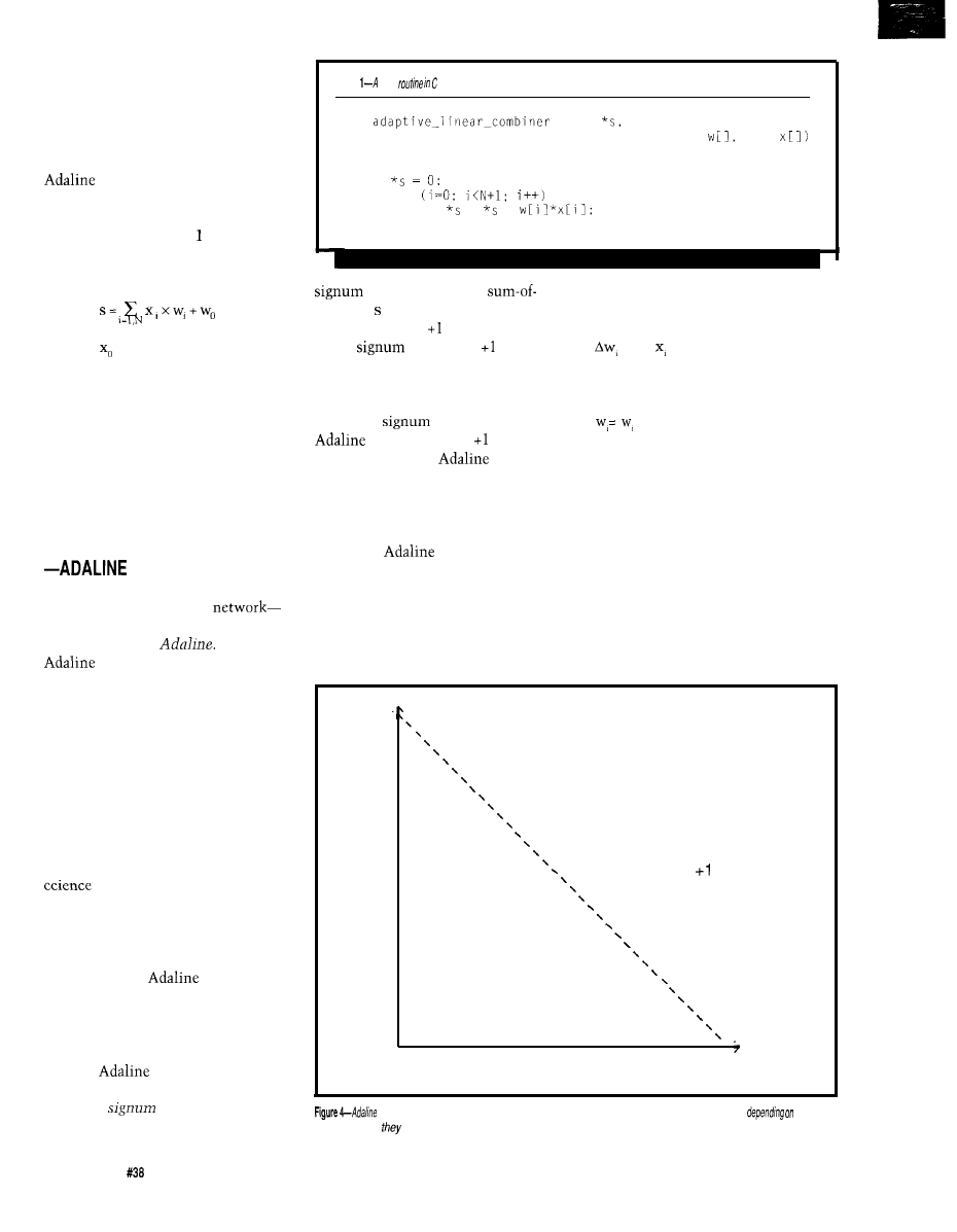
finally calculates the sum of these
products.
Listing
1
shows a small snippette
of C code that implements the adap-
tive linear combiner (the complete
source and executable code for the
and Madaline programs are
available on the Circuit Cellar BBS).
This is a simple array multiplication
and addition. Equation describes the
adaptive linear combiner and is
defined as:
(I)
=
1
(always)
The arrow facing toward the left
side of Figure 2 shows an error calcula-
tion. The error is the difference
between the output and the target, or
correct answer. We will use the error
to adjust the values of the weight
vector w. The adjusting process is how
the neural network learns.
THE ADAPTIVE LINEAR ELEMENT
Figure 3 shows an example of one
type of elementary neural
an adaptive linear element-which is
also known as an
The
is a linear classifier, which
means it can distinguish patterns that
are linearly separable. Figure 4 shows
an example of two classes that are
linearly separable. Figure 5 shows the
numbers that were used to create the
graph in Figure 4.
Suppose we had data on the
success of students at a summer
computer camp. The result could be
that shown in Figure 4. The students
who scored high on both math and
tests fared well in our com-
puter camp.
The two classes of students in this
example are linearly separable since I
can draw a straight line that separates
the classes. The
can adapt to
this data and then predict the success
of future computer camp students
based on their math and science
scores.
The
has the adaptive
linear combiner plus these two new
parts: the
function and the
alpha-LMS learning algorithm. The
Listing
short
illustrates the implementation of the
Adaptive Linear Combiner.
long
(long
long N,
long
long
long
i;
for
= +
function takes the
products and transforms it into a
binary output of or
-1.
The output
of the
function is if the
input is greater than or equal to zero,
and -1 otherwise. The code in Listing
2 shows the subroutine that imple-
ments the
function. The
can only have a or -1
output because the
separates
or classifies data into two classes. You
must design your problem to fit this
limitation.
the training patterns, hence the name
LMS [least mean square).
= a x x error
for i = l,N
(2)
error = target-s
0.1 <a<
1 . 0
t
Aw
for i = l,N
(3)
Equations 2 and 3 describe the
alpha-LMS algorithm. They illustrate
how to multiply the error by an input
and an alpha factor
to
produce the
change in each weight. The factor
alpha is a constant that is set between
The alpha-LMS learning algorithm
is how the
learns or adapts its
weights to the correct answer. It
0.1
and 1.0. If you set alpha too high,
considers the error and the x-inputs
the learning process will generate
and automatically produces the
oscillations and never reach an end. If
necessary changes in the weights. The
you set it low, the learning will
alpha-LMS algorithm works by trying
progress very slowly. You must
to minimize the mean square error in
experiment with this. The code in
Math
Scores
X
9 0
X
xx
X
Class =
8 0
X
7 0
xxx
X
Separating
Class= -1
Line
60
.
Science
60
7 0
8 0
9 0
100
Scores
iscapable
of distinguishing students who scoredhigh in math andscience,
which
side of the line
fall.
38
Issue
September 1993
The Computer Applications Journal
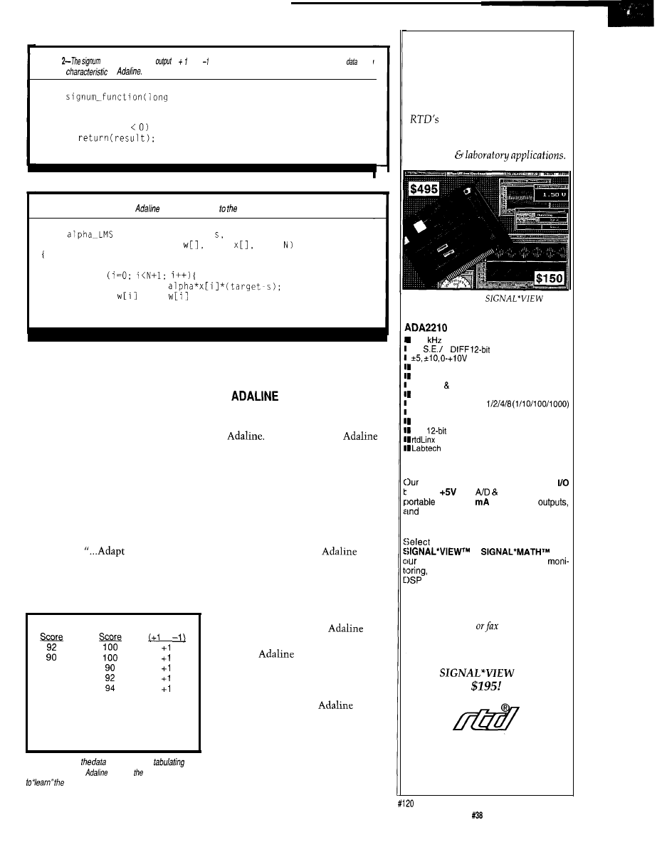
Listing
function uses a binary
of or to establish the classification of being
used, a
of
long
input)
long result = 1;
if (input result = -1:
Listing
3-An example of how
adapts ifs weights correct answer using alpha-LMS is shown.
long
(long target, long float alpha,
long
long
long
long delta-w, i;
for
delta-w =
=
+ delta-w;
Listing 3 shows a simple routine
written in C that implements the
alpha-LMS algorithm.
Equations 2 and 3 and the code in
Listing 3 are the “magic potion” that
allows neural networks to learn. They
form the basic feedback loop that
In other words, adapt the weights, but
do not disturb them too much.
adjusts the weights until the network
produces correct answers. You can
initialize the weights to small random
numbers, then use the alpha-LMS
algorithm as a feedback loop to
dynamically adapt them.
The alpha-LMS algorithm uses the
principle of minimal disturbance,
which states
to reduce the
output error for the current training
pattern, with minimal disturbance to
responses already learned...” [Widrow].
program and interact with menus until
you are comfortable with the interface.
The first step when using this program
is to enter the data. For this exercise,
type in the 10 sets of data given in
Figure 5. The file names you choose
are completely arbitrary. The next step
AN
EXAMPLE
is training the network. Choose this
option and watch as the
loops
I’ll use the data in Figure 4 and
through the data until it can produce
correct answers for all 10 inputs.
Figure 5 as an example of how to use
an
First run the full
Math
Science
8 8
88
8 6
72
6 8
70
70
70
70
72
80
82
84
Class
or
-1
-1
-1
-1
-1
Figure
5-Taking
from Figure 4,
if,
and feeding if fo the
allows neural
network
desired task.
The final step is processing new
data cases not included in the original
training set of Figure 5. Enter any set
of points and see how the
classifies it. You can easily find a case
where the
gives a wrong
answer. This is because we only used
10 sets of data for training. The more
data that is used in training the
network, the better the
will
perform.
THE MULTIPLE ADAPTIVE
LINEAR ELEMENTS-MADALINE
Figure 6 shows a more complex
and capable neural network using
Data Acquisition
and Control
Without Compromise
Programmable Scan &Burst
Advanced Industrial Control
boards set a new performance
standard for general purpose
industrial
ADA2210 with
A cost-effective solution
features:
125
XT throughput
I 16
8
analog inputs
I
selectable input range
programmable auto channel scan
programmable burst mode
I software external triggers, pacer clock
on-demand DMA transfer
I programmable gain:
I3 cascadable 16-bit counters
16 programmable digital I/O lines
two
analog outputs, selectable range
Universal TSR DOS driver
Notebook driver
HARDWARE SOLUTIONS
AIC family also includes AT analog
Boards,
only
control boards for
PCs, 4-20
current loop
opto-22 compatibility.
SOFTWARE SOLUTIONS
the power and performance of
or
from
library of application programs for
data acquisition and analysis, control,
and 3D graphics.
For more information on these and other
ISA bus and
PC/l 04
products,
call, write
us today!
Place your order now and receive
SIGNAL*MATH and
for
Real Time Devices, Inc.
P.O.
Box 906
State College, PA 16804
(814) 234-8087
n
Fax: (814) 234-5218
The Computer Applications Journal
Issue
September 1993
39
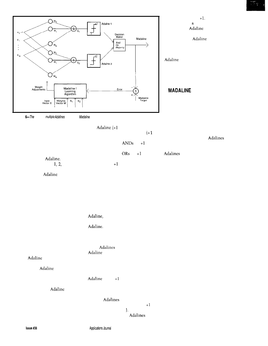
output
2
-1
output
Output
Figure
use of
is known as
multiple Adalines-this kind of
network is known as a Madaline. The
Madaline in Figure 6 contains only
two Adalines, but it could have as
many as you want. I built the
Madaline using the adaptive linear
combiner and the
Therefore, I
can use code segments
and 3 from
those devices. The Madaline is more
capable than the
because it
can separate patterns that are not
linearly separable.
Figure 7 gives an example of
patterns that are not linearly separable.
Consider the data in Figure 4 and
Figure 5, and suppose the computer
campers at the high and low ends of
the math and science scores did better
than the rest in computer music. The
bent line drawn in Figure 7 shows the
two classes of computer music
campers. If we trained the Madaline to
separate these patterns, we could use
future math and science scores to
predict computer music success.
The
cannot distinguish
the two classes shown in Figure 7.
Recall that the
can only
distinguish classes that are separable
by a single, straight, dividing line.
The Madaline has two new
components that the
did not
have: the AND, OR, MAJORITY
decision maker and the Madaline-Z
learning algorithm. The AND, OR,
MAJORITY decision maker decides
the final output. It takes the outputs of
each
or
-1)
and determines
the final output of the Madaline
or
-1).
If you use the AND decision
maker, it logically
the and
-1
inputs. If you use the OR decision
maker, it logically
the and
-1
inputs. The MAJORITY choice counts
the number of and
-1
inputs and
chooses the most popular input. The
AND, OR, MAJORITY decision maker
is a simple device you can build using
Adalines. The code in Listing 4
implements the decision maker in
software.
The Madaline-I algorithm (you
may be interested to know that there
are three different Madaline algo-
rithms) adjusts the weights of the
whose and
-1
output
disagrees with the Madaline target,
and whose s output is closest to zero.
For example, suppose the Madaline
The second new part of the
Madaline is the Madaline-I learning
had five
and the Madaline
algorithm shown in Listing 5. In the
we used the alpha-LMS
produced an incorrect output of (the
algorithm to adjust the weights of an
The Madaline is a little more
correct target was
-1
The Madaline-I
complex, however. How are the
weights of this network adjusted? Are
algorithm looks at the
that
the weights of only one, several, or all
of the
adjusted? Which
is adjusted? How is that done?
had outputs equal to
Next, it
examines their outputs (equation
1)
and finds the
whose s is
closest to zero. Now it adjusts the
weights of that
using the
alpha-LMS algorithm shown earlier.
Train the Madaline by using your
input data sets and adjusting the
weights until it produces
correct answers for all cases. Imple-
menting the Madaline-I is a simple
matter of coding the algorithm in
Listing 5.
A
EXAMPLE
I’ll use the data in Figure 7 and
Figure 8 as an example of how to use a
Madaline. First, run the Madaline
program and interact with it through
the menus. Next, enter the data given
in Figure 8. The file names you choose
are arbitrary.
The next step is training. You
must specify how many
you
want in the Madaline. I chose seven,
but feel free to experiment. The more
in the network, the more
power it has, but this also slows down
the performance of the network. You
must also select the AND, OR, or
MAJORITY decision maker. I chose
MAJORITY. After choosing your
options, watch as the Madaline loops
through the data until it can produce
correct answers for each of the
10 sets
of data.
The final step is processing new
data cases not in the original training
set. Enter any set of points and see
how the Madaline classifies it. Once
again, it is easy to select points that
produce a wrong answer because we
only used
10
sets of data for training.
The previous examples with
computer campers gave you an idea of
the use of neural networks, but now
let’s move to something more con-
crete-money. An excellent use of
neural networks is examining loan
applications and deciding which loans
to approve or disapprove. Loan officers
often make poor decisions because,
being human, they sometimes con-
sider nonessential factors that can
mislead them. Considerations such as
A REAL-WORLD EXAMPLE:
LOAN APPLICATIONS
40
September1993
The Computer
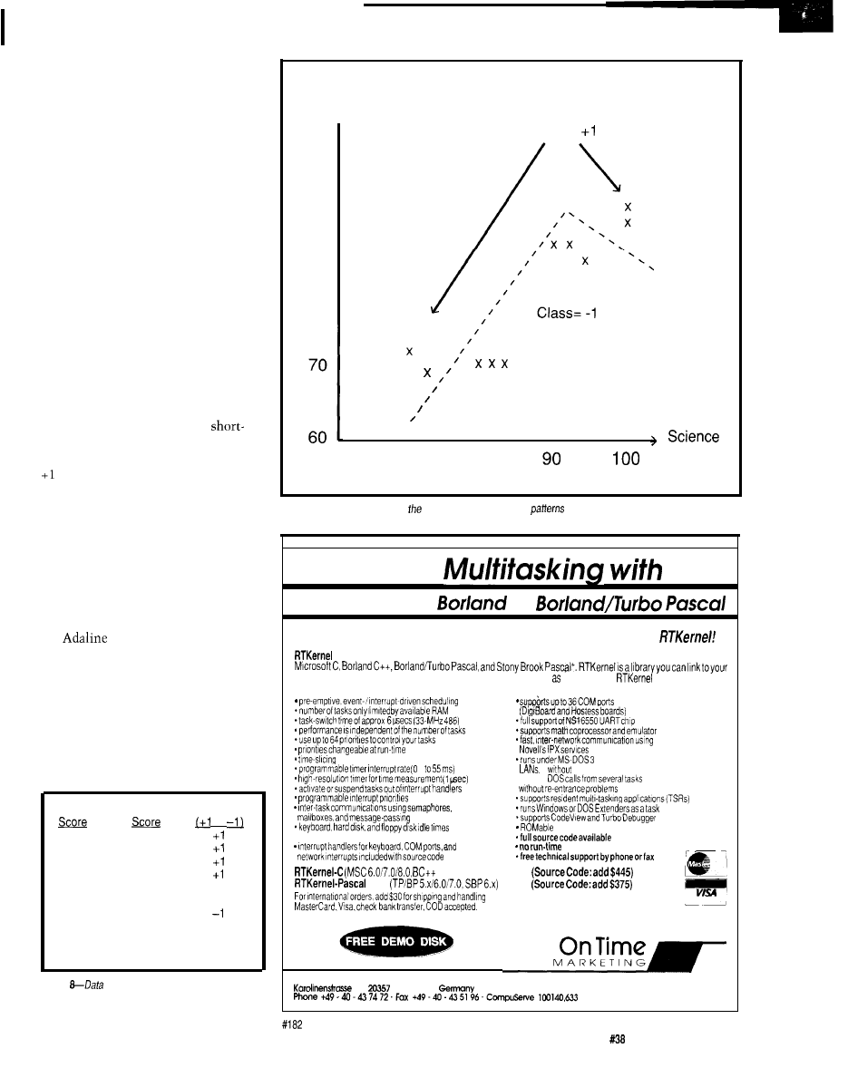
appearance, dress, speech, politics, and
family connections can sway loan
officers, and sometimes the result is a
bad loan.
The loan application problem is
well suited for neural networks for
several reasons. First, there is an
abundance of training data. Banks keep
their completed loan application
forms, and of course they remember
whether or not an approved applica-
tion was successful.
This history will be the training
data set. Also, the loan application
data are either numerical or can be
easily transformed into numbers. Facts
such as age, income, and debt are
numbers, and you can transform
occupation, address, and credit record
into number-codes very easily,
Figure 9 gives sample data sets for
the loan application example. The
bank has this information for
term $20,000 loans. Borrowers paid off
five of the loans on time [these are the
cases), and defaulted on five of the
loans [these are the -1 cases). I’ll use
these as training data and then predict
the success or failure of future loans. If
the network predicts a loan will be
successful, then I’ll approve that
application.
The first step is to input the data
in Figure 9. Then run the Madaline
program [this is a nonlinear problem so
the
cannot solve it) and enter
the 10 sets of data. Each set of data has
four elements and a target. We plotted
the data sets and separating lines for
the two previous examples on X-Y
axes because they only had two
elements per data set. Plotting the data
of Figure 9 requires a drawing with
four axes and a separating object. I’ll
Math
Science
Class
or
7 2
7 0
6 8
7 2
9 2
100
9 0
100
8 8
9 0
- 1
8 8
9 2
- 1
8 6
9 4
70
8 0
- 1
7 0
8 2
- 1
70
8 4
- 1
Figure
can be used
in conjunction
with Figure
7 to run the Madaline program.
Math
Scores
,
100
90
80
Class =
60
70
80
S c o r e s
Figure 7-When using Madaline,
capability of differentiating
not linearly separable is possible.
Real- Time
DOS
for Microsoft C,
C,
Develop Real-Time Multitasking Applications under MS-DOS with
is a professional. high-performance real-time multitasking kernel. It runs under MS-DOS and supports
application. It lets you run several C functions or Pascal procedures parallel tasks.
offers the following
advanced features:
can beactivated
0t06 0. DR-DOS.
1
or
operating system
*perform
usablebyothertasks
royalties
1.012.013.x)
$ 4 9 5
$445
M A R K E T I N G
Professional Programming Tools
3 2
H a m b u r g
The Computer Applications Journal
Issue
September 1993
41
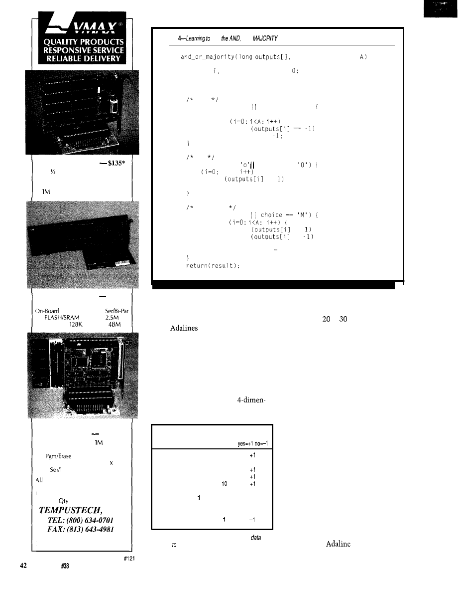
SOLID STATE DISK
Card 2 Disk Emulator
EPROM, FLASH and/or SRAM
Program/Erase FLASH On-Board
Total, Either Drive Bootable
25MHZ 386DX CPU
$695’
Compact AT/Bus or Stand Alone
SVGA, IDE, FDC, 2
Drives to
Cache to
DRAM to
TURBO XT
w/FLASH DISK
$266”
To 2 FLASH Drives,
Total
DRAM to 2M
FLASH On-Board
CMOS Surface Mount, 4.2” 6.7”
2
Par, Watchdog Timer
Tempustech VMAX’ products are
PC Bus Compatible. Made in the
U.S.A., 30 Day Money Back Guarantee
*QTY
1,
breaks start at 5 pieces.
INC.
Fax for
295
Airport Road
fast
response!
Naples,
FL 33942
Listing
use
OR,
decision maker is straightforward.
long
char choice, long
int
minus = 0, plus =
long
result = -1;
AND
if (choice == ‘a’
choice == ‘A’)
result = 1;
for
if
result =
OR
if (choice ==
choice ==
for
i<A;
if
==
result = 1:
MAJORITY
if (choice == 'm'
for
if
== plus++;
if
==
minus++:
if
(plus > minus) result I:
leave that as an exercise for the
reader-it is possible.
The next step is training. I used
seven
in the Madaline and
the MAJORITY decision maker. The
Madaline learned the training data in
less than a minute.
The final step is processing new
loan applications. Once again, it is
easy to enter an example that produces
a “wrong” answer. I quoted wrong in
this case, because with this
sional problem I am not sure which
Income
#Years Current
Approve?
$k Age Employed Debt$k
60
40
15
5
55
35
13
7
tl
50
30
8
3
70
42
20
12
65
45
22
30
40
15
20
-1
25
22
1
-1
20
30
7
10
-1
22
25
2
15
-1
15
20
1
Figure 9-A
real world application consists of
important a loan officer.
Issue September 1993
The Computer Applications Journal
domains are right or wrong answers.
My advice is train the network with a
minimum of or sets of data,
especially if you are a loan officer.
CONCLUSION
I’ve discussed the basics of neural
networks and showed how to use
them. There are three properties to
remember about neural networks.
They can be used to recognize and
separate patterns, are simple to
program, and are adaptable.
Neural networks (and people]
perform pattern recognition tasks
much better than traditional computer
approaches. Simulating a neural
network in software is not difficult.
The short, simple code listings given
here show the heart of the neural
network. Once you have the neural
network program, you use it to solve
many different problems. You train the
network to solve new problems just
like I did when I trained the Madaline
to solve the problems I illustrated.
Most of all...definitely do experi-
ment! Use the
and Madaline
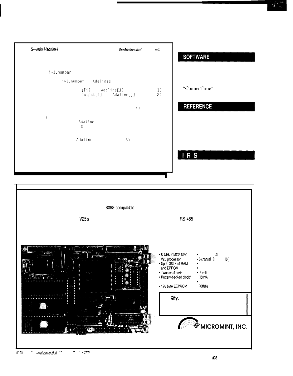
programs on new problems. These
market prices, predicting the weather,
programs use integer arithmetic and
are very flexible. Predicting stock
and optical character recognition are
good experiments.
q
Listing
Learning
Algorithm, weights are adjusted in
disagree
the
Madaline target.
Do until Madaline's output = target for all training cases
Do for
of training cases
Do for
of
in Madaline
calculate
for
(code listing
calculate
for
(listing
calculate Madaline output (code listing
If Madaline output != target Then
Find the
whose output != target
and whose is closest to zero
Use the alpha-LMS learning algorithm
on that
(code listing
Repeat all the training for all the
training cases
Dwayne Phillips works as a computer
engineer with the U.S. Department of
Defense. He has a Ph.D. in Electrical
and Computer Engineering from
Louisiana State University.
Software for this article is avail-
able from the Circuit Cellar BBS
and on Software On Disk for this
issue. Please see the end of
for downloading
and ordering information.
“Thirty Years of Adaptive Neural
Networks: Perceptron, Madaline,
and Backpropogation,” Bernard
Widrow, Michael A. Lehr, Proceed-
ings of the IEEE, Vol. 8, No. 9,
September 1990, pp. 14151442.
407 Very Useful
408 Moderately Useful
409 Not Useful
V25 POWER COMES TO EMBEDDED CONTROL!
Micromint’s RTCV25 is the perfect marriage of an
processor, programming convenience, and control I/O. Forget
the need for cross-assemblers and cross-compilers; your favorite high-level language for the PC and a “locate” facility are all you
need. The RTCV25 enhances the
power with parallel I/O; A/D conversion; RS-232 and
serial ports; up to 384K of
RAM and EPROM; a battery-backed clock/calendar; 128 byte EEPROM, ROM monitor, and the RTC stacking bus. Ease of code
development combined with its small size and low power consumption make the RTCV25 ideal for all embedded control applica-
tions. And of course the RTCV25 is compatible with Micromint’s full line of RTC peripheral boards and products.
Features:
calendar
40 parallel lines
(or bit ADC
RTC stacking bus
Small 3.5" x 5" size
only operation
max.)
Full featured
ROM monitor
l
operating system
100
OEM configuration
$270
4
Park St.
l
Vernon, CT 06066
call
l-800-635-3355
(203) 871-6170
l
Fax: (203) 872-2204
See
Systems Booth #
The Computer Applications Journal
Issue September 1993
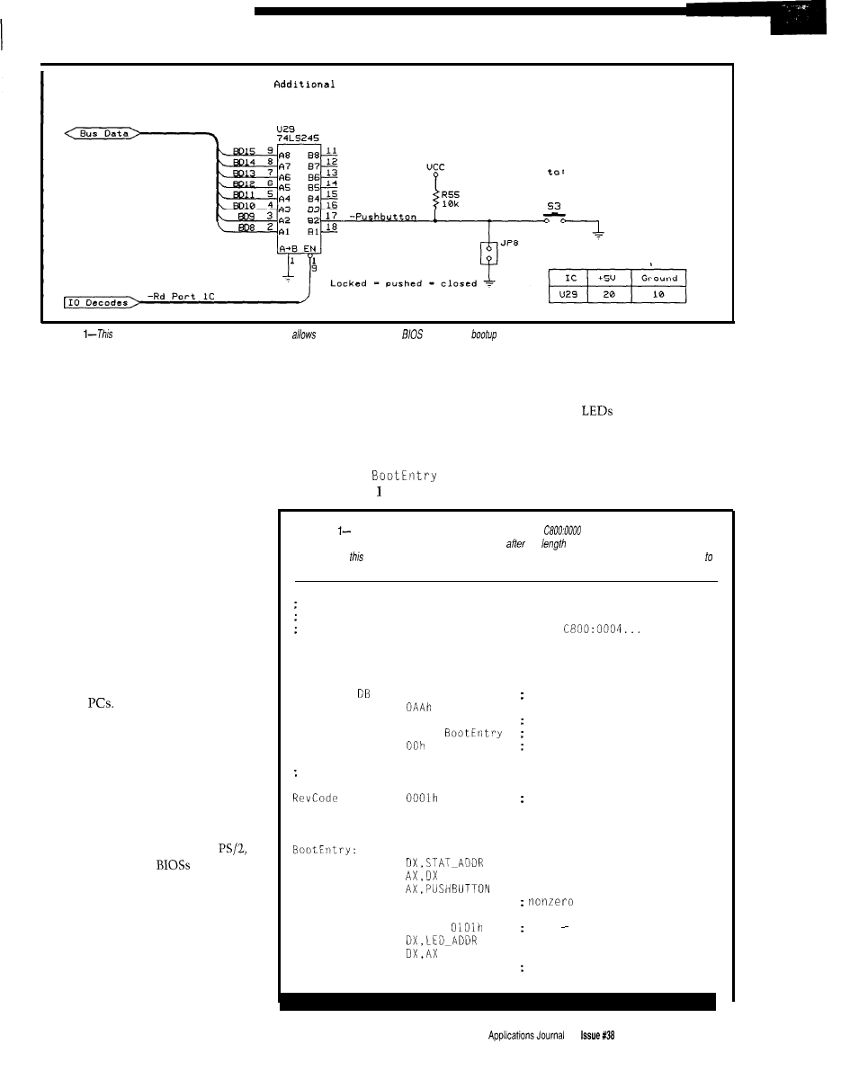
c i r c u i t r y s h o w n
i n p r e v i o u s a r t i c l e s . . .
P u s h b u t t o n
E n a b l e B I O S e x t e n s i o n d i s k l o a d
D i s a b l e B I O S e x t e n s i o n d u r i n g b o o t
T o f r o n t p a n e l
“ k e y b o a r d i n h i b i t ’
k e y - l o c k s w i t c h
Power Table
Figure
month's hardware, a button and a resistor,
you to skip over a new
extension at
should if continually crash the system.
Should you ever come up against a
length, and checksum bytes required
into all your extensions, at least during
“locked” clone, just whip out your
for the BIOS scan. Recall that the
debugging. If the switch is pressed [or
Swiss Army knife’s Phillips blade,
checksum byte in the source code
the lock is on) while booting, FDB EXT
unscrew the clone’s case, yank out
must be zero, because our diskette
updates the
and returns to the
those pesky little wires on the lock
boot loader computes the value as it
BIOS. This can save your bacon if your
switch, and you’re on the air. I trust
copies the extension into the Firmware
new extension crashes the BIOS boot
I’m not compromising the security of
Development Board.
sequence. Trust me, it can happen.
what was once the Free World by
The code at
is the
Assuming the switch is off, the
letting that trick out of the bag. The
escape hatch that suggest you build
code shown in Listing 2 makes the
Original AT’s lock switch disabled the
keyboard and secured the metal cover
to prevent just such an assault.
So much for the hardware. Now,
on to the code..
EXTENSION ESSENTIALS
The Original PC BIOS didn’t scan
for extensions, which led to some truly
remarkable kludges as each vendor
devised unique and mutually incom-
patible ways to glue new functions
into old
The method used now
dates back to a revision of PC BIOS
slightly before the XT, so, for all
intents and purposes, every PC handles
it the same way now.
If you are designing video adapters
there is a more recent technique to
ensure your extension will be initial-
ized first regardless of its address. The
method, devised by IBM for its
is
not supported by all
and is
beyond the scope of my column, but
check the references for more details.
It might come in handy if you need
control right away, but unless you’re
running a “true blue box,” the compat-
ibility issues warrant some care.
The part of FDBEXT. ASM shown in
Listing
1 sets up
the 55 AA signature,
Listing This code is loaded into the battery-backed
RAM
at
on the Firmware Development
board. The B/OS passes control to the instruction just
the
byte during the power-on sequence.
The first thing
code does is check the pushbutton-switch bit; if the button is pressed the code returns
fhe BIOS.
This does not start at offset 0100, so be careful
about data accesses!
Actual execution is at absolute address
CODESEG
STARTUPCODE
055h
signature
DB
DB
2
length in units of 512 bytes
JMP
SHORT
force two-byte jump
DB
loader sets this value
constants that must be stored within the checksummed region
D W
current revision level
;- if pushbutton is down, exit without doing much
MOV
IN
TEST
JNZ
SHORT Continue
means not pushed
MOV
AX,NOT
show to track our path
MOV
OUT
RETF
return to normal BIOS boot
Continue:
The Computer
September1993
45
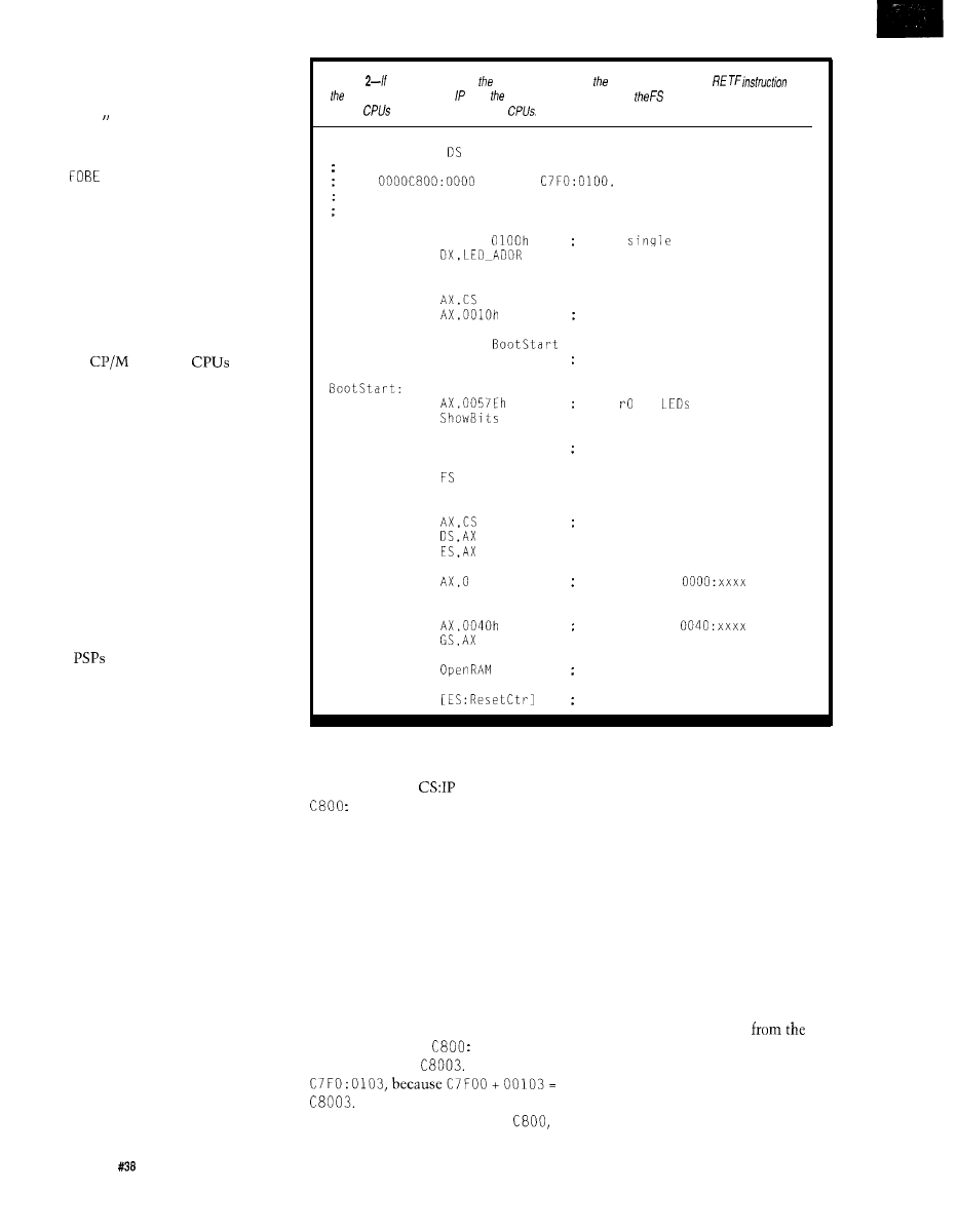
whole software development process
I’m using for this series work cor-
rectly. As Steve puts it, “Let me
explain..
THE CASE OF THE MISSING PSP
XT
is written in Borland’s
Turbo Assembler using the TINY
memory model to produce an ordinary
COM file. As far as TASM and the
linker are concerned, the program will
run under DOS, so all the usual DOS
assumptions and restrictions apply.
As you know by now, COM files
are exact binary images of the
program’s code. They date back to the
days of
and 8080
when
64K of RAM was all you had even if
you were a big spender. The operating
system reserved the first 256 bytes of
RAM to get control of the 8080’s reset
and interrupt vectors, so your pro-
grams were loaded at address 0 100.
MS-DOS adopted the same
memory layout, except that 64K was
suddenly not so much after all. A
COM file fit neatly into one 64K
segment atop the reserved 256 bytes,
which, still filled with operating
system stuff, became known as the
Program Segment Prefix. Executable
(EXE) files are handled differently:
their
live in a different segment,
and we’ll get to them later, but for
now the key point is that COM files
start at 0 100 for historical reasons.
Although all of the code and data
addresses within a COM file assume
that it’s loaded at offset 0100, the
actual disk file does not include those
first 256 bytes. The instruction at
program offset 0 10 0 is thus at 0 0 0 0
relative to the start of the file. DOS
must set up the segment registers so
the offsets are correct within the
segment where the program is loaded.
The disk boot loader introduced in
issue 3 1 simulates this process. It
loads your program from diskette at
address 10 0 0 : 0 10 0 with nothing in
the first 256 bytes. Although there’s no
PSP, that trick let us use standard
COM files without a specialized
linker. As long as the program didn’t
expect anything in the PSP, its absence
makes no difference.
BIOS, on the other hand, knows
nothing of this. When it finds our
Listing
the switch is open,
next step is to adjust segment
registers. The
loads
new values info CS and from stack. Note: This code uses and GS segment registers found
in ‘386
and will not run on earlier
;- adjust CS and to simulate the normal COM situation
We need both code and data starting at offset 0100 rather
than
is also
so we just subtract
0010 from the segments. Storing this CS in the vectors
allows normal access after an interrupt
MOV
MOV
OUT
AX,NOT
show
here
DX,AX
MOV
SUB
PUSH
PUSH
RETF
AX
OFFSET
MOV
CALL
PUSH
DS
PUSH
ES
PUSH
PUSH
GS
MOV
MOV
MOV
MOV
MOV
FS,AX
MOV
MOV
CALL
INC
enable writes
count this reset
adds 100 to offsets in segment
set CS and IP to new values
show on
to mark entry
preserve seg regs
set up DS to match CS
FS
points to
GS points to
Firmware Development Board exten-
sion, it passes control to that branch
instruction with
set to
0003. Because we’ll be setting
interrupt vectors as well as changing
data, our code must somehow adjust
all the segment registers.
The solution is a simple matter of
subtraction. A given physical address
can be accessed by many different
segment and offset values. The CPU
simply shifts the segment register left
by four bits, adds the offset, and uses
that as the physical address. At least
that’s the case in real mode, which is
all we need for now.
The branch at
0003 is at
physical address
It is also at
Thus, if we reload the segment
registers with C7 FO rather than
all our offsets are correct and we can
use COM files for BIOS extensions.
The easiest way to reload both CS
and IP is from the stack with a RET F
(Far Return) instruction. Listing 2
shows the trick in all its glory.. .not
very impressive to see, is it?
COM programs assume that CS,
DS, ES, and SS all have the same value,
but CS and DS are the key registers. I
load DS and ES from the adjusted CS
value, but SS cannot aim into the non-
volatile memory because it is normally
write protected.
Fortunately, as long as we just
PUSH,POP,CALL, and RET
stack, whatever the BIOS uses for SS
and SP will work fine. I haven’t looked
at how deep the default stack is, but
you might want to check it out if you
need lots of room for some reason.
46
Issue
September 1993
The Computer Applications Journal
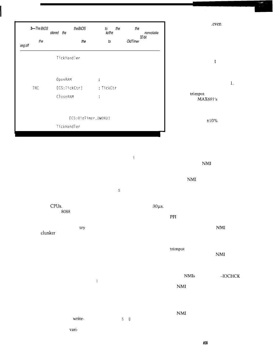
Listing
extension captures
timer interrupt count ticks since most recent
reset. The value of CS
in interrupt vector allows access extension’s variables in
memory. Because this code was assembled in 386 mode, the INC instruction increments a
counter in
one shot, and final JMP instruction requires SMALL keyword specify that
contains a
address.
PROC
PUSH
PUSH
CALL
CALL
POP
POP
JMP
ENDP
AX
DX
enable writes
is 32 bits wide
disable writes
DX
AX
SMALL
Although it’s not written down
anywhere, BIOS requires that you
restore at least DS and ES in addition
to CS, which is loaded by the final
RETF. I save and restore all the
segment registers even though the
actual requirements surely depend on
which BIOS you’re using.
FDB EXT also marks a departure
from the code you’ve seen so far:
notice that I’m now using the FS and
GS segment registers that appear only
in '386 and higher
As a result,
this code will not run on
or
80286 systems. I don’t include any
tests for the CPU type, as I assume
we’re all adults around here.
Don’t
it on your old
PC just to see
what happens.. .it won’t work!
Yes, FDB EXT could be written to
work on any 80x86 CPU, but it’s time
to start using hardware that’s been
around since 1985. OK?
CAPTURING INTERRUPTS
The remainder of F D B E X T's
initialization code captures the BIOS
timer and nonmaskable interrupt
vectors. This is standard code that
you’ve seen before, so I won’t waste
space on the listings.
Listing 3 shows the timer inter-
rupt handler. The Firmware Develop-
ment Board’s RAM is normally
protected, so each handler must enable
the RAM before updating the
ables. The CS segment stored in the
interrupt vector is the same as the DS
value set up in Listing 2, so the I NC
instruction can “reach” T c
k C t r
using CS without having to save, load,
use, and restore DS.
Because the RAM write-enable bit
shares the same port as the watchdog
timer bit, it is easy to have the Open
RAM and C
1 o e
RAM toggle the watch-
dog on each BIOS timer tick. Measur-
ing the bit’s active time shows that the
interrupt handler requires about
As I mentioned in the last col-
umn, it’s generally not a good idea to
toggle a watchdog from a timer
interrupt because the main routine can
crash without affecting the timer tick.
However, this will keep the watchdog
at bay while loading a
big
program
from diskette. The mainline code can
always capture the timer tick and
implement my favored method after it
starts running.
Enabling ‘386 assembly mode has
some interesting side effects. The
T c
k
C t
r
variable is a double word, but
the assembler uses the 32-bit version
of I NC to update it in one instruction.
The
JMP
at the end of the routine
passes control to the previous inter-
rupt handler, but you must specify
SMALL to tell the assembler that the
vector represents a
e : 0 f f
value
instead of a 32-bit LARGE offset in the
current segment.
I like that sound..
in real
mode!
FAILING POWER
The BIOS extension responds to
power failures by write-protecting the
RAM and spinning in a safe loop.
While writing this code uncovered a
nasty bug-NM1 glitches. While these
shouldn’t pose a problem in most
systems, it’s worth thinking about
them if you’re using the MAX69
The Firmware Development Board
includes a
to adjust the
voltage on the
PFI pin. The
correct setting activates the Power Fail
Output when the supply voltage falls
near the system’s lower tolerance
limit; say -5% on a
system. The
remaining 5 % gives you enough time
to shut the system down before the
supply goes out of tolerance.
In small systems, the MAX691 is
the only source of nonmaskable
interrupts, but, as I described in the
last column, many parts of a PC
contribute to the
signal. Our
handler must examine the board’s
power failure status and chain to the
previous
handler. Only when the
PFO bit is low can the handler shut
down the system.
Here’s the problem: if the supply
voltage falls slowly enough, a small
supply glitch that would normally be
well within tolerance can trigger the
comparator and generate a
nonmaskable interrupt. By the time
the CPU responds to the
and
checks the PFO status bit, however,
the glitch is long gone. You can
simulate this by adjusting the PFI
very slowly.
Because none of the
sources
are active, the default BIOS handler
gets control. Guess what? On my
system, the default handler disables
further
from the ISA
signal! So when the power really fails,
the
handler never gets control.
If the FDB is the only source of
IOCHCK interrupts in your system,
your interrupt handler can check the
status bit in port 0x6 1 to verify that
the
came from the bus. Because
that status bit is latched when
IOCHCK goes active it does not go off
when the glitch vanishes.
The Computer Applications Journal
Issue September 1993
4 7
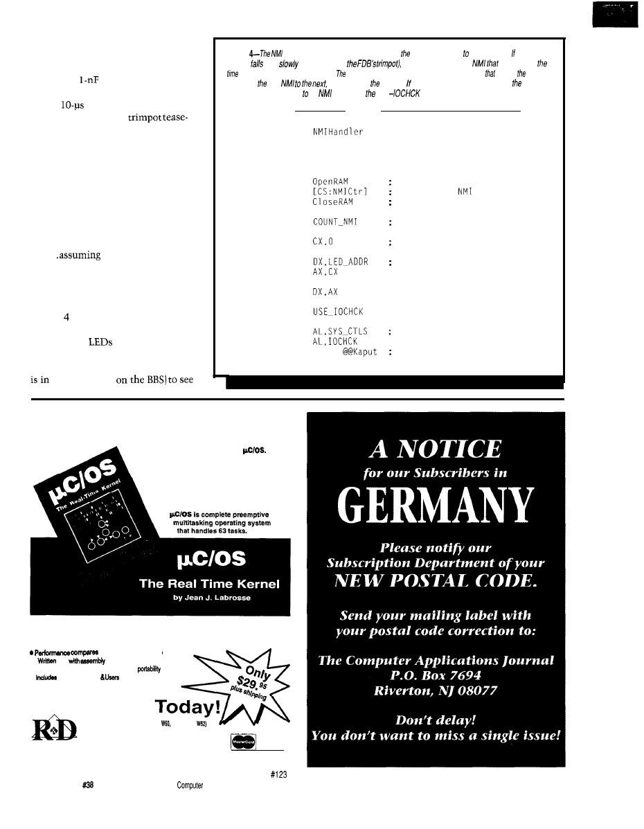
However, if you have several I/O
cards that can produce IOCHCK
interrupts, the situation is a little
messier. A
capacitor on the PFI
trimpot’s wiper filters the glitches
with a
time constant. On my
system that made the
proof, but you should evaluate it to
make sure it does not delay the
interrupt too much during a real power
failure on your system.
An alternative approach would be
some hysteresis on the PFI pin.
Because PFO switches low as PFI
drops, a resistor between the two pins
will yank PFI down and prevent the
end of the glitch from restoring
PFO..
the comparator’s
propagation time doesn’t glitch it the
other way!
In any event, one of the condi-
tional assembly options shown in
Listing is a timing loop that starts
on the first NMI. It display the loop
count on the
until the next
NMI, at which time it locks up the
system. You can use that code [which
EXTTEST.BIN
Listing
handler normally shuts down system in response a power failure. the supply
voltage
very
(or if you tease
you can get a glitch on
vanishes by
this handler gets control. code shown here includes an optional section displays elapsed
time from first
then locks up system. this is a problem in your system, code can
a/so lock up in response an
caused by ISA
input
@Wait:
PROC
PUSH
PUSH
CALL
INC
CALL
IF
MOV
MOV
MOV
NOT
OUT
IF
IN
TEST
@Kaput: JNZ
AX
DX
AX
SHORT
enable writes
record this
disable writes
show delay?
set up the counter
show the loop counter in binary
look at IOCHCK flag
lock up when it goes high
(continued)
Push the Limits of Real-time Design!
Investigate the fundamentals of building
real-time embedded kernels with
Written in C with minimum assembly
code, it is portable and ROM able.
Learn about task priority scheduling,
intertask communication, interrupts,
and performance benchmarking.
Secrets of Embedded Systems Revealed!
to commercial kernels
l
in C
code
minimized
l
Assembly code minimized for easy
l
System Cod-9
Manual
q
Companion Disk for $24.95
Order
(order
book
book a
disk
913-841-1631
publications, inc.
FAX 913-841-2624
50
issue September
1993
The
Applications
Journal
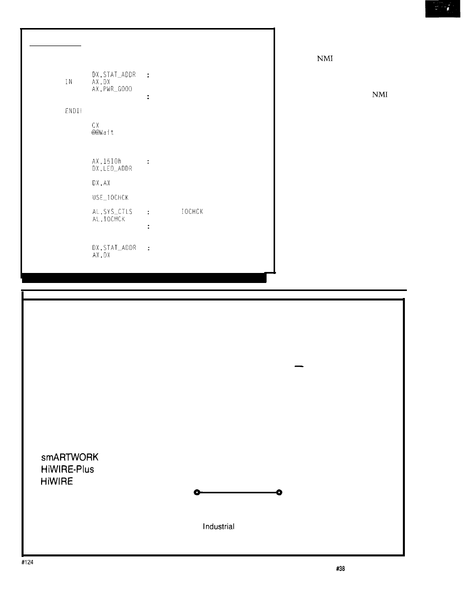
Listing
4-continued
ELSE
MOV
TEST
@Kaput: JZ
check power status
SHORT @@Kaput
lock up when status goes low
INC
JMP
ELSE
MOV
show ni (more or less)
MOV
NOT
AX
OUT
IF
IN
TEST
JNZ
ELSE
look at
flag
SHORT @Lockup lock up when it goes high
MOV
IN
check power status
(continued)
how this problem looks on your
system.
The CPU disables all interrupts
within the
handler, so the
watchdog timer isn’t updated in the
final lockup loop. The MAX691 will
time out and reset the system about
1.6 seconds after the second
occurs.
RESETS AND THE WORST HACK
The Original AT’s designers had a
problem. They needed a way to get
their new 80286 CPU back to real
mode even though the chip had no
way to shut off its protected mode
enable bit. The 80826 emerged from
hardware reset in real mode, but once
the program entered protected mode
there was no way back. Their solution
is
a testament to engineering ingenu-
ity.
The AT included an 8042
microcontroller to handle a variety of
tasks that were done with discrete
logic in the Original PC. The designers
added a command to the 8042’s
repertoire that toggled the 80286
EXPRESS CIRCUITS
MANUFACTURERS OF PROTOTYPE PRINTED CIRCUITS FROM YOUR CAD DESIGNS
TURN AROUND TIMES AVAILABLE FROM 24 HRS
2 WEEKS
Special Support For:
l
TANGO. PCB
l
FULL TIME MODEM
l
TANGO SERIES II
l
GERBER PHOTO PLOTTING
l
TANGO PLUS
l
PROTEL AUTOTRAX
l
PROTEL EASYTRAX
l
WE CAN NOW WORK FROM
YOUR EXISTING ARTWORK BY
SCANNING. CALL FOR
DETAILS!
l
l
II
Express
l
EE DESIGNER I
l
EE DESIGNER III
l
ALL GERBER FORMATS
Circuits
1150 Foster Street
l
PO. Box 58
Park Road
Wilkesboro, NC 28697
Quotes:
l-800-426-5396
Phone: (919) 667-2100
Fax: (919) 667-0487
The Computer Applications Journal
Issue
September 1993
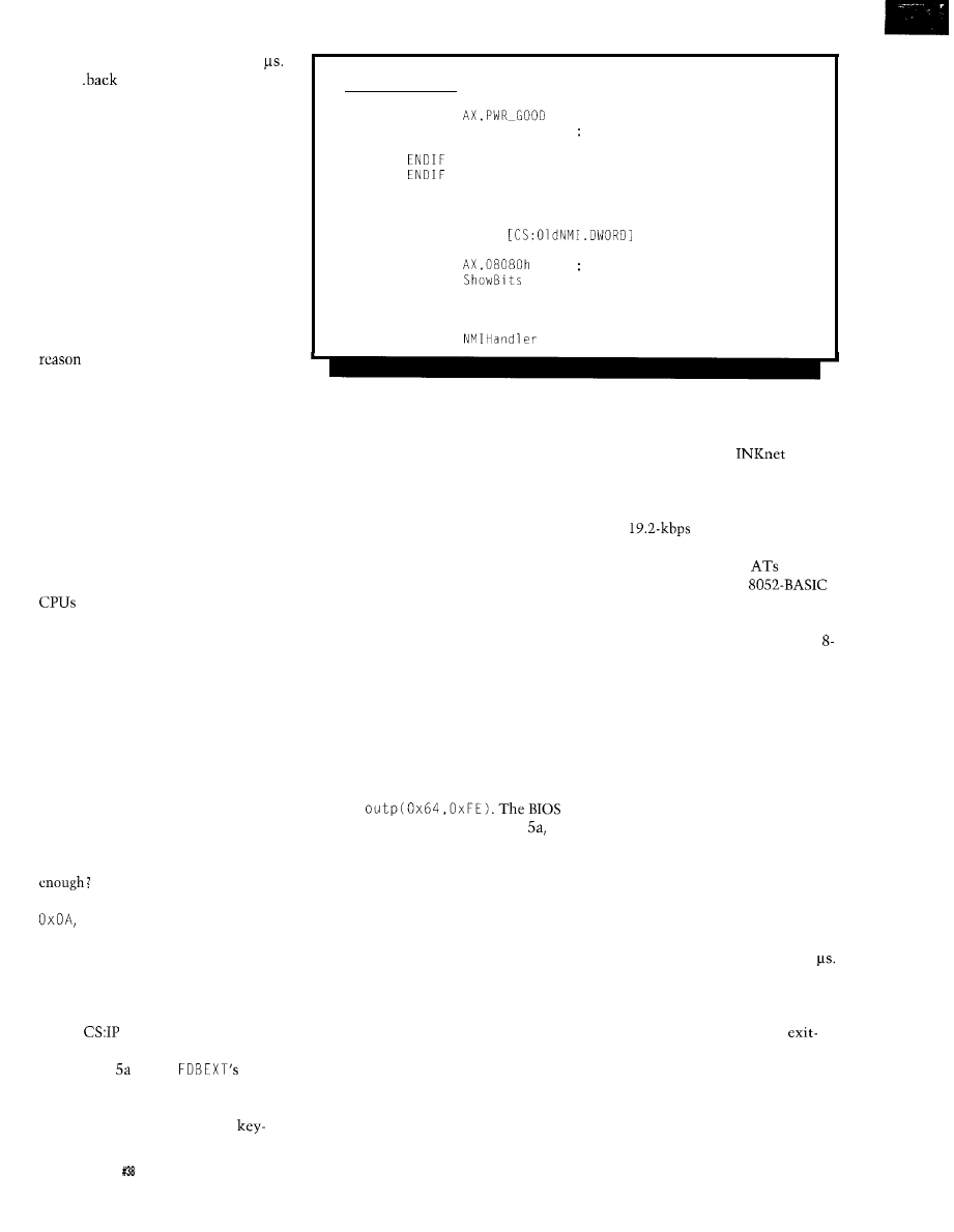
CPU’s reset line active for about 6
Blam..
to real mode!
But the BIOS normally clears the
system RAM and runs power-on
diagnostics immediately after a
hardware reset, which is not quite
what they wanted. So they reserved a
byte at address 0x0 F in the real-time
clock’s battery-backed CMOS RAM to
indicate the reason for the shutdown.
Before the BIOS gets too far, it
asks the keyboard controller why the
system was reset. If the controller says
that it executed a reset command (as
opposed to a power-on or front-panel
reset), the BIOS reads the shutdown
code. If that byte indicates a
protected-to-real mode transition, the
BIOS branches directly back to the
mode switch routine.
The only reason you think it’s a
kludge is that you didn’t design it. It’s
really a clean, general, and useful way
around an otherwise insurmountable
hardware limitation. Remember: you
don’t get paid if the system doesn’t
work!
Intel got the message loud and
clear: starting with the 80386 all their
enter and exit protected mode at
the flip of a bit. By now, though a
considerable body of software uses the
‘286 method, so you can buy
hyperthyroid keyboard controllers
with special fast-path hardware logic
to recognize and speed up the reset
command. I kid you not.
The shutdown reason code can
select one of several different routines
after a reset. Most of them are not
suited for civilian use, but one may
come in handy in certain desperate
situations. I’ll show how to use it, you
figure out when it’s appropriate. Fair
If the shutdown reason code is
the BIOS vectors through the
value stored at address 0 0 4 0 : 0 0 6 7.
Because the system RAM isn’t affected
by the brief shutdown, you can regain
control immediately after a hardware
reset. Of course, all the registers
except
are lost, so there are a few
minor details I’ll leave as an exercise.
Listing shows
rudimentary restart routine, which
simply increments a counter and sends
another reset command to the
Listing 4-continued
TEST
JZ
POP
POP
JMP
@@Lockup:
MOV
CALL
@@Stall: JMP
ENDP
SHORT @@Lockup zero = power NOT good...
DX
AX
SMALL
both decimal points
@@Stall
board controller. The BIOS clears the
shutdown reason code before branch-
ing to the routine, so it treats the
second reset as a complete power-on
reset.
Although the restart handler is in
nonvolatile RAM (it must be there
when it’s needed!), it seems that
F D B E X T cannot load the vector. At
least on my system, the restart vector
changes after F D B E X T exits, although
the shutdown reason code does not. So
FDB E XT puts the address it would have
used in a spot that EXTTEST knows
about.
Listing 5b shows the code from
E X TT E S T that transfers the vector from
nonvolatile RAM to address 0 0 4 0 :
0 0 6 7 and sets the shutdown reason
code. Later, in response to a keyboard
command, E X TT E ST simply executes
the following instruction to reset the
system:
then executes the code in Listing
goes through a second reset with all
the normal power-on tests, and reloads
EXTTEST from diskette. That’s all
there is to it!
So if anybody asks you about the
worst hack in PC-dom, you can say
you’ve been there and done that. Be
sure to tell me if you put it to good
use!
A CAUTIONARY TALE
I have often advised you to read
the data sheets carefully. Generally I
do a lot of reading before starting a
project, but once in a while, well..
This tale shows that hell hath no
fury like that of an unjustified assump-
tion.
Those of long memory will recall
the series of articles on
back in
late 1989 (“A Network for Distributed
Control,” Circuit Cellar INK, issues
10-12). To summarize, the networks
used a
RS-485 serial link to
connect up to 32 nodes. I wrote a
monitor program for IBM
that
acted as a console for the
nodes and displayed network status
information. All in all, a neat project.
Because the design point was an
MHz AT from IBM, running a network
at 1920 bytes/second posed some
interesting challenges. Because an AT
runs at about 1 MIPS, there are only
about 500 instructions between each
byte. If you get distracted for a milli-
second or so you will lose data.
Each transmitted byte actually
generates two interrupts because the
RS-485 network echoes data back to
the receiver. The first interrupt occurs
when the transmitter buffer goes
empty and the second, very shortly
thereafter, blinks on when the receiver
buffer fills with the same character.
The elapsed time varies, but it can be
as little as one bit-time, or about 50
Because the two interrupts occur
so close together, I polled for inter-
rupts at the end of the handler to
eliminate the lengthy interrupt
and-entry overhead if the byte was
ready. My ‘scope showed that this
worked quite well: most of the time,
each character produced only one
interrupt.
52
Issue September1993
The Computer Applications Journal
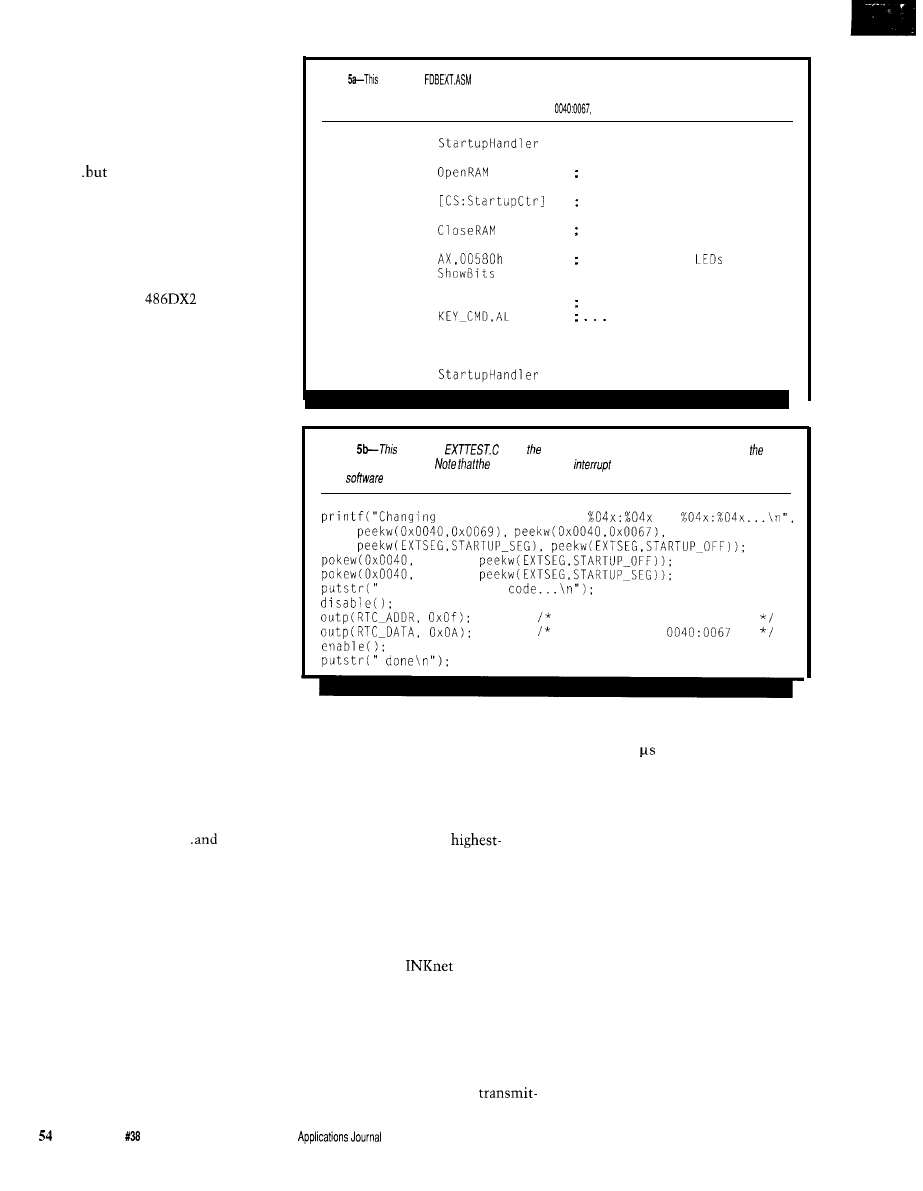
About a year later, though, some
customers reported sporadic problems
with network errors that we simply
couldn’t duplicate. Some of the
problems were due to cabling, some to
terminations, others to severe
noise..
there was a very small
minority of customers with everything
set up right and everything still going
wrong.
The problems seemed more severe
on faster machines. Finally, this year
one customer installed the software on
his new 66-MHz
and reported
that it failed in a matter of minutes.
Ah ha! The bug must be related to
CPU speed, because, in this case, we’d
eliminated everything else.
I set up a test network on my
then-new 33-MHz ‘386SX (yes, the
same one I’m using for these embed-
ded ‘386SX projects], activated the
trace outputs built into all my code,
hitched up the logic analyzer, and
waited to see what happened. After a
long wait, the TSR got jammed in an
“impossible” state.
Although my system wasn’t as
fast as the latest 486 CPU, the logic
analyzer showed that each outbound
character generally produced two
separate interrupts. Progress had
eliminated the need for my interrupt
polling trick and I was glad to get rid of
it. However, very rarely, the second
interrupt (the one caused by the
receiver buffer) was suspiciously long.
I modified the TSR code to
produce trace outputs for each possible
interrupt source and discovered that
the “long” interrupts were caused by a
change in the modem status register.
That was peculiar, as the TSR did not
enable MSR interrupts..
the
Interrupt ID Register should not report
a disabled interrupt.
Essentially, all PCs use National
Semiconductor 8250, 16450, or 16550
serial interface chips or an LSI chip
that works just like them. I pored over
the data sheets in search of something
I’d missed three years ago. What could
cause an invalid IIR! I assumed that
my code was at fault, as genuine
hardware problems are very, very few
and far between.
In the 8250 family, transmitter
interrupts are cleared when you read
Listing
code in
gains control after the keyboard controller blips the CPU's reset
line. The BIOS checks the shutdown reason code at address OF in the real-time clock’s CMOS RAM; if that
value is OA it vectors through the address stored at
which EXTTEST aims at this routine.
PROC
CALL
enable writes
INC
record another startup
CALL
disable writes
MOV
show r. on the
CALL
MOV
AL,OFEh
tell kbd controller
OUT
to blip the reset line
@Stall: JMP
@Stall
ENDP
Listing
code from
loads vector and sets fhe shutdown reason code info real-
time clock’s CMOS RAM.
vector is nof in the
fable because if is neither a hardware
nor a
interrupt.
startup vector from
to
0x0067,
0x0069,
setting shutdown
aim at shutdown reason code
vector through
the IIR or write a new character, but
receiver interrupts are cleared only
when you read the pending byte. You
would expect, as I did, that the
Interrupt ID Register is updated almost
immediately. You would be
almost
correct.
ter interrupts. Should the receiver
cause the interrupt, however, it may
take up to
1
to flip the summary bit
after reading the character. The
interrupt request output pin has the
same timings, so the IIR bit must be
wired to the output driver rather than
the actual input bits on the chip.
The IIR reports the
priority pending interrupt, but bit 0 is
a summary status flag that, when
zero, means “there is at least one
interrupt active.” My code reads the
IIR and uses it as an index into a
decoding table. Only two interrupts
can occur in the
TSR, but,
being a belt and suspenders type, my
table has all possible entries. That
saved my skin!
Upon close scrutiny, the 16450
data sheet reveals two key timings.
The summary bit is updated within
250 ns of reading the IIR for
As Sherlock puts it, “When you
have eliminated the impossible,
whatever remains, however improb-
able,
must be the truth.”
A sufficiently fast CPU can
respond to the interrupt, read the IIR,
branch to the receiver handler, read
and process the byte, and check the IIR
again before the summary bit changes.
Because the receiver interrupt bit is
cleared almost immediately, the IIR is
invalid.
As you might guess, an all-zero IIR
indicates a modem status interrupt.
Issue September 1993
The Computer
I checked my references again to
Indeed!
see if anyone else knew about this.
The serial port in my 33-MHz
The only hint was in Mark Nelson’s
‘386SX is just one corner of an LSI
Serial Communications: A
chip, but ISA compatibility barnacles
Developer’s Guide, published in 1992
dictate exactly how it must work. In
(well after I needed it). In 8250
this case, the barnacles require new
ties he states:
silicon to precisely duplicate the same
annoying bug found in
old bugs! Aren’t standards great?
both the original National
There are no good fixes for this, so
chips as well as some clone
I used a time-honored kludge: a delay
chips is the false modem status
loop. The code measures the CPU
interrupt. The IIR can report a modem
speed when it installs the TSR and sets
status interrupt when none has
up a delay loop that occupies at least a
occurred. This could easily lead to
microsecond. After each receiver
trouble with the ISR code..
interrupt, it stalls long enough to
I don’t want to find out how can save a lot of money using
ROM-DOS 5 instead of MS-DOS@ in our 80x86 product line.
don’t care if ROM-DOS 5 iscompatible with MS-DOS 5 but
costs much less. I
like
spending much more than I have to.
It makes me feel like a philanthropist and besides Microsoft@
probably needs the money more than I do anyway.
q
IYes
I want to know the facts about ROM-DOS 5.
Please send me information and a free bootable demo disk to
try with my software.
the
U.S.A.
or
fax this coupon to (206) 435-0253.
Name
Company
A d d r e s s
State
Zip
ensure that the IIR interrupt summary
flag is valid. Not pretty, but it works.
The moral of this story is twofold:
RTFM first, then build trace outputs
into your code so you can see what’s
going on. But any regular reader of this
column knows that already, right?
RELEASE NOTES
The BBS files this month include
the
loader to start “applica-
tion” programs from diskette and the
special AD E X T loader to put a BIOS
extension into the
nonvolatile
storage. You also get FD B EXT and
whole process works. The comments
explain how to load and run the code.
Next month I’ll add a small
character LCD to the Firmware
Development Board so you can display
messages without a serial port. I’ll also
give each FDB a unique serial number
to make up for stealting the keyboard
lock switch. This may smell like copy
protection, but in the embedded
systems world there are some excel-
lent reasons to make sure your code
runs only on the right machines!
q
Ed Nisley, as Nisley Micro Engineer-
ing, makes small computers do
amazing things. He’s also a member
of
the Computer Applications
engineering
staff.
You
may reach him
on CompuServe at
or
through the Circuit Cellar BBS.
If you’ve gotten this far in the
project you should have no
trouble finding a pushbutton
switch. Pure Unobtainium has the
complete Firmware Development
Board schematic, as well as
selected parts. Write for a catalog:
Pure Unobtanium
13 109 Old Creedmoor Rd.
Raleigh NC 276 13
Phone/fax: (919) 676-4525
410
Very Useful
411 Moderately Useful
412 Not Useful
The Computer Applications Journal
Issue
September 1993
5 5
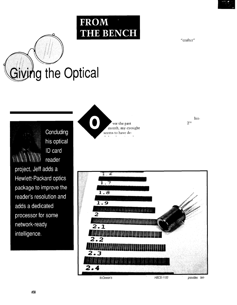
Jeff Bachiochi
Card
Reader Improved Vision
graded to the point where
I thought a checkup was in order. I
couldn’t understand how my vision
could fail so rapidly. I tossed around
thoughts trying to pinpoint a cause.
Could it be a change in diet? No, I am
still having my weekly pizza fix. How
about the weather? Well, it is hotter
and I am swimming more, but Crystal
Lake doesn’t have chlorine.
It is the obvious we tend to
overlook. The glasses I wear have
round lenses. The lens
was
kind enough to put a slight notch on
the lens where it should line up with
the frame joint. While cleaning my
eyewear this morning, I noticed the
lens was gradually rotating in the
frame. After realigning the notches, I
could see clearly again.
RECAP
Last month, I discussed optical
coding techniques and some methods
for printing optical swipe codes using
standard character graphics. I showed
you how a two-byte character string
could be encoded on a small credit
card, and how it could be read using
inexpensive microsensors. The
checked code is capable of
(65536)
different combinations.
INCREASING RESOLUTION
Higher quality optics can increase
the focusing power for both the
transmitter and receiver, which
enables detection of objects with a
finer resolution. The more concen-
trated the area of illumination is at the
Photo l-Compared
optical sensor, the Hewlett-Packard
sensor package
a
fold improvement in detection of a barcode.
56
Issue
September 1993
The Computer Applications Journal
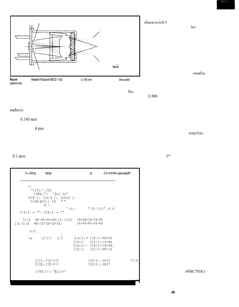
Emitter
Detector image through
emitter lens
Maximum
signal point
Emitter imaae through
detector
Detector
l--The
focuses a single
spot 4 mm in front of the
assembly.
focal point, the smaller a nonreflective
spot can be that prevents reflective
detection. The HBCS-1100 from
Hewlett-Packard uses a bifurcated
lens to image the active areas
of a visible LED and photodetector to a
single
spot, that is focused 4
mm in front of the lens. This is neatly
packaged in an
TO-5 can. HP’s
sensor is $27.00 (single piece) as
opposed to Omron’s at $4, but the
specs are also in a different league. (see
Photo and Figure 1)
If you assume a barcode that uses
a
line and 0.2-mm space, the
HP sensor should be able to read about
60 bits/inch (about 8 bytes, or 4
checked bytes/inch). This indicates
that a factor of 10 improvement is
realized over Omron’s device. The
HBCS-1100 includes an internal
transistor which can (optionally) be
used as a high-gain amplifier to the
photodiode.
WHAT GOOD IS FINER
RESOLUTION IF YOU CAN’T
PRINT A LABEL?
A printer’s character graphics are
limited to 80 character columns per
8.5 inches (or 132 character columns
in condensed mode]. This comes up to
10 N =
20 WIDTH
30 LPRINT
+
40 DIM
50 M$ =
=
60 FOR X = 0 TO
70 PRINT "Enter hex number
INPUT
80
90 NEXT X
Listing
spacing
with the HP LaserJet, it’s possible achieve a
without resorting to using graphics mode.
100
=
=
=
SE28 =
120 FOR X = 0 TO N-l
130 V =
140 FOR Z = 3 TO 0 STEP
150 IF AND
=
THEN
=
ELSE
160 NEXT Z
170 NEXT X
180 LPRINT
TO N-l
190 LPRINT
TO N-l
200 LPRINT
210 LPRINT
220 END
=
LPRINT
X: LPRINT
LPRINT
X: LPRINT SE28
about 15 characters per inch (132
inches) which is just
about equivalent to 1 byte of
checked data/inch. This is about the
minimum size we could detect with
the inexpensive microsensors using a
slit mask. So how can we print these
small swipe codes?
The vertical line character is the
thinnest possible line which can be
printed. The problem is not so much
with printing this character, but in
printing each character with a
than-normal character-to-character
width. This calls for some special
carriage control. The LaserJet is
capable of carriage movements down
to
of an inch. Listing 1 was used
to print multiple characters with a
varying amount of back carriage
movement between characters. Using
visual inspection, I chose a carriage
movement that left a space approxi-
mately equal to the width of the
character to assure detection. This
spacing measures about 0.3
space width.
It may not sound like a major
improvement, and compared to
magnetic densities it’s a joke, however
we now have different possible
combinations within the same density.
Not bad for the home-brewed ap-
proach.
CUT DOWN A FEW NOTCHES
It isn’t too often you hear anyone
advertising their failures. If I didn’t feel
there was lesson here, I would bury the
following experiences deep within my
research paperwork. But, since I think
there is something to be learned here,
I will humble myself and share it with
you all. The project I had in mind was
a black box which would read optical
swipe cards, and respond either by
beeping an error tone or by performing
some other function. The functions
that would be performed might
include storing the card sequence;
comparing the card sequence to a list
of acceptable sequences, unlocking a
door, notifying a remote computer,
allowing the remote to “OK” the card
sequence, and so forth.
My plan was to use a
or a PIC processor to act as a net-
worked node of the swipe reader
The Computer Applications Journal
Issue
September 1993
57
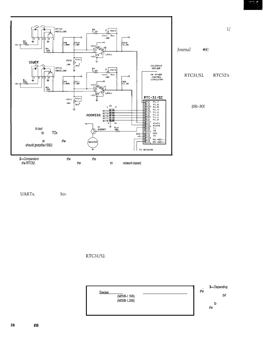
UPPER TRACK 1
T R A C K 0
Correction:
month’s schematic,
the
connections
the Of
devices
were
incorrect. The K lead of each
device should go ground
while A
lead
resistor.
Figure
are used to
clean
up raw
signal from optical
sensors. The squared-off signals then drive interrupt
lines on
The single-board computer adds intelligence necessary make a
stand-alone unit.
system. My hardware requirements for
this node were a built-in UART or
multiple timers and external inter-
rupts. None of the small processors
have
which means
banging a serial port. That’s fine, but I
can’t lose interrupts from the optical
tracks, either. I decided to break this
into two independent operations. The
first would be responsible for reading
the swipe tracks and verifying a valid
read. The second would handle the
serial network and talk to an EEPROM
which would hold a list of acceptable
data sequences.
I spent a few days writing optical
data code and the interprocessor
nybble port (for communications
between processors), I spent a few
more days writing network code and
debugging the interprocessor nybble
port, then a day or so on EEPROM
routines. I linked the routines together
and received an “attempt to use
nonexistent memory.” Do I add a third
processor in parallel to handle the
EEPROM routines? This was starting
to smell a bit like it was turning into a
parallel processing article. Good
material, but not what I started out to
accomplish.
So this is what it’s like when you
can’t fit ten pounds into a five-pound
bag. It always fit before. Oh well, from
now on I’ll severely overestimate the
size of my code, just to be safe!
NOW WHAT?
Let’s
take a moment and review
the requirements again. I needed a
UART, some nonvolatile memory, a
couple of interrupts, and some form of
network hardware. Well, this list of
requirements could be met with the
Nothing lowers the cost of
a design like using the hardware over
and over for a variety of tasks. I guess
the wide range of applications is what
gives single-board computers their
universal value. For those of
you who are curious or are
not familiar with the RTC3
52, see “From the Bench” in
the April/May 1989 issue of
the Computer Applications
(issue
for the
schematic.
Figure 2 shows the
schematic for the swipe
circuit and how it connects to
the
The
built-in BASIC interpreter is
used for the foreground task
of analyzing the network
“command strings.” If a
command string with its own
address
is recognized,
the appropriate response is
given back to the network.
Supported commands are:
Query-a list of all
completed swipe data
sequences
List-a numbered list of all
acceptable data se-
quences
Clear-clear the list of
acceptable data se-
quences
Add-add an acceptable data
sequence
Delete-delete a particular data
sequence
The original approach, using an
EEPROM, had room for 64 two-byte
entries. Using the RTC52 with a
nonvolatile RAM increases this to
thousands. Also, the original system
could store only a single swipe. This
meant any network master had to keep
on its toes and be ready to jump at a
moment’s notice. Now, there is plenty
of buffer space which takes a big
burden off of any network master.
Since improved resolution allows
more than the initial two bytes of data,
the system can be configured to read
two or more bytes of data from a single
Figure
on
direction
Which bit has the actual data
direction a card is
1
forward
first bit
swiped and which has
2
forward
complement bit
the actual data,
four
3
backward (LSB-MSB)
first bit
ways
exist actually
4
backward (LSB-MSB)
complement bit
collect
data.
Issue
September 1993
The Computer Applications Journal
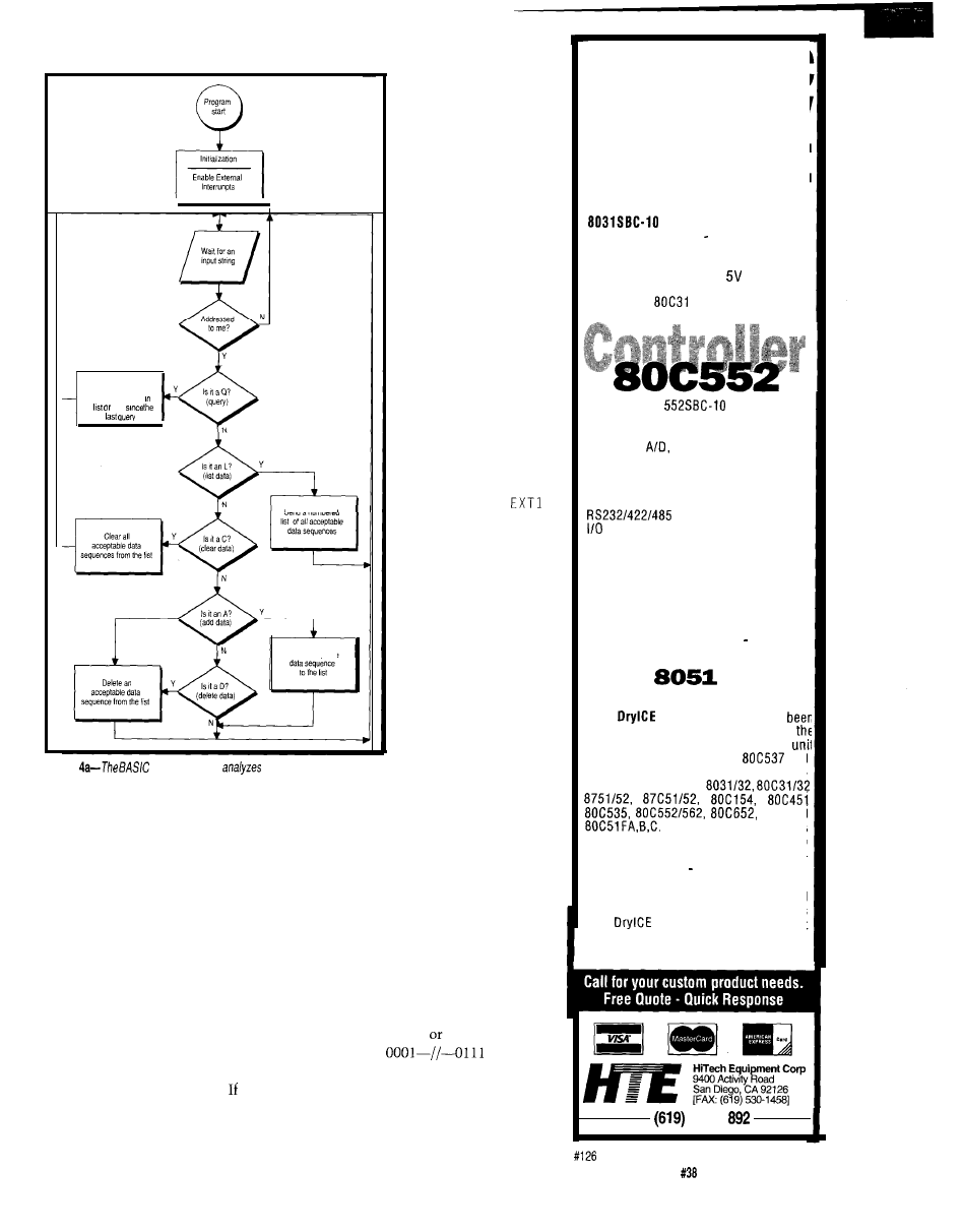
Send any good
data sequences
(whether they were
the not)
Send a numbered
Add an acceptable
Figure
foreground
task
the network
command
strings and acts on the supported command set.
card. The number of stored sequences
goes down proportionally to the
sequence length, but there is still
plenty of room to go around.
HIGH-PRIORITY TASKS
Two interrupt routines are written
in machine language. The first is the
T I ME RO overflow interrupt. This
routine is responsible for identifying
when a swipe is completed. If the
overflow counter reaches its maxi-
mum count and an error or an uncom-
pleted read has been flagged, then an
error beeper is strobed and things are
reset to await another swipe. a good
read was confirmed, the data sequence
is transferred to the queue and a
comparison is per-
formed against all the
acceptable data se-
quences in the list
buffer. If a match is
made, an output bit is
strobed enabling a door
latch (or other device). If
no match is found, the
error beeper is strobed
and things are reset for
the next pass.
The TIMER0
interrupt is enabled and
the timer is cleared each
time the external
interrupt routine is
entered, thus preventing
a timeout. This routine
can be entered by either
one of the two external
interrupts. EXTO is
triggered by a mark on
the lower track.
is
triggered by a mark on
the upper track. The
data bit is set to a “0” or
“1” by the correspond-
ing interrupt.
Three steps are
necessary to complete a
good swipe. First, the
start sequence needs to
be recognized. Since all
data bits are sent once,
complemented, and
sent again for confirma-
tion, a start sequence
cannot be confused with
data. Second, a start
sequence has at least three consecutive
bits of the same logic state followed by
one complemented bit. The last bit is
used to flag the direction of the card
swipe.
Third, the end sequence must be
the complement of the start sequence
but in the reverse order. Thus, the only
two possible start and end sequences
are:
111 O--//-l 000
The data is of a known length,
which is a function of sensor resolu-
tion, printer resolution, and card size.
8051 SBC
AT A
NEW
LOW
PRICE
We are proud to offer our standard
Single Board Computer
at a new, low price just $79 per unit
or as low as $49 each for quantity pur-
chases. An 8031 with two JEDEC
sockets, one RS232, regulator,
expansion connector. Optional second
serial port,
or 32.
At $149, our
has the price
and features you need right now! It’s an
8051 core processor with an eight chan-
nel, IO-bit
two PWM outputs, cap-
ture/compare registers, one RS232, four
JEDEC memory sockets, and more digital
I/O. And we didn’t stop there! You can
add
options
like
two
more
ports, 24 more digital
ports, Real-Time Clock, EEPROM,
and battery-backup for clock and RAM
right on board. Start with the Develop-
ment board; it has all the peripherals
plus a debug monitor for only $349.
Download and debug your code right on
the SBC, then move to the OEM board
above for your production needs. We
also do custom design work call for our
reasonable prices.
New
Family
Emulator Support
O u r
P l u s p r o d u c t h a s
expanded to include support for
Siemens 806537. The base emulation
is still only $299, with the
pod
priced at $199. Other 8051 family proces-
sors supported are
a n d
Each of these pods is
priced at $149. Where else can you get an
emulator with this much power and flexi-
bility for only $448 complete?
Our original stand-alone 8031 ICE is still
priced at $199. Though not as flexible as
the
Plus, it offers excellent
price/performance for learning or the
occasional job need.
666-l
The Computer Applications Journal
Issue September 1993
59
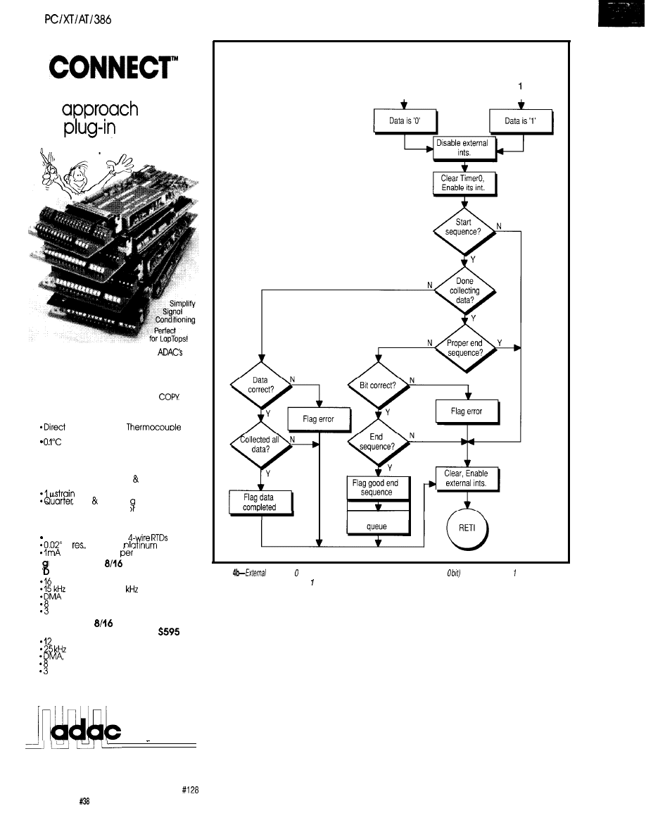
Users!
DIRECT
A time-cutting
to
data
acquisition
Save valuable project time with
DIRECT CONNECT’” data acquisition
modules. FREE DIRECTVIEW” Board
Tutorial and Data Acquisition software
means a shorter learning curve and
quicker results. CALL FOR A FREE
Thermocouple 8 Channel
A/D Board
$650
Connection to
wires and shields
resolution
*Software selection of J,K,T,R,S,&B
Strain Ga
8
e 8 Channel
A/D Boar
$795
*Direct Connection to 3 4 wire
Strain Gages
resolution
Half Full brid e completion
*On-board excitation vo taae
RTD 8 Channel
A/D Board
$795
Direct Connection to
C
100 ohm
current source
channel
Hi h Resolution
Channel
A/ Board
$895
bit A/D resolution
throughput (50
option)
lines digital I/O
channel counter/timer
Multifunction
Channel
A/D Board
bit A/D resolution
throughput
Prog Gain
lines digital I/O
channel counter/timer
Many other models available, Call:
I-800-648-6589
corporation
70
Tower Office Park, Woburn, MA
01801
FAX (617) 938-6553 TEL (617) 935-6668
External
0
External
interrupt
0
interrupt
0
Start
sequence?
Y
Transfer data to
Figure
interrupt is triggered by a mark on the lower track (a and external interrupt is triggered
by a mark on the upper track (a bit).
The data is expected as “bit” and
“complemented bit” to ensure data
integrity. There are actually four ways
data can be collected (Figure 3).
I use the first data bit when
reading forward, and the complement
when reading backward. When the
data sequence is transferred to the
queue, I reverse the sequence if the
read direction was backward. Any data
that falls outside of the expected logic
state sets the error flag. You can see
the algorithm for the program I wrote
for the swipe card reader in Figure 4.
TIME STAMP
You could easily add local time
stamping to each entry, or you could
allow the remote master to time stamp
query polls (providing it does polling in
a timely fashion).
Stand-alone operation (meaning
that no computer is necessary to load
the acceptance list) could be added to
the security door application. This
could be accomplished by assigning a
master “add” and “delete” card
sequence to the program that would
place the unit in a mode to alter the
62
Issue September 1993
The Computer Applications Journal
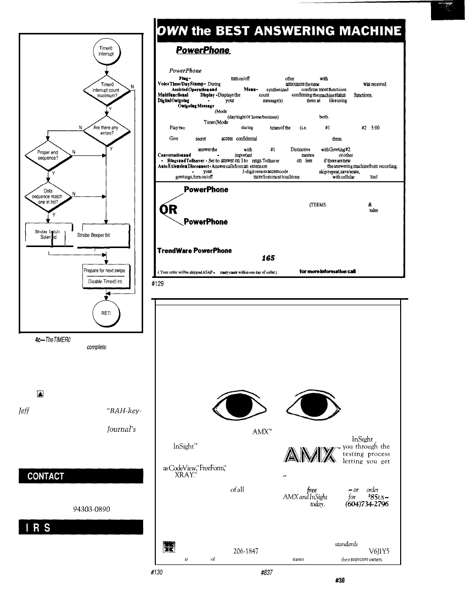
,
,
Figure
interrupt routine
is responsible
for identifying when a swipe is
acceptable data sequence list by just
swiping cards through. That is,
provided you are playing with a full
deck.
Bachiochi (pronounced
AH-key”) is an electrical engineer on
the Computer Applications
engineering staff. His background
includes product design and manufac-
turing.
Hewlett-Packard
P.O. Box 10301
Palo Alto, CA
413
Very Useful
414 Moderately Useful
415
Not Useful
The
is a full featured answering machine,
including remote power On/Off control of your PC.
The
includes all these features and more:
AC Power
Call-in
and remotely
your computer (or
AC devices)
any touch-tone phone.
message
play, a synthesized voice
and day each message
Voice
Remote Voke
The
voice
LCD
message
along with
and
Messages
Record
own outgoing
and change
you
digital technology.
5
Posslbk
Modes
.
Two Outgoing Messages
1 and 2)
Record two “going messages
and switch between
. Outgoing Message
3)
different outgoing messages
selected
day.
Greeting at 8:00 AM and at
PM)
l
Voice Mail (Mode 4)
callers a
code to
a
message (mailbox) you record only for
l
Distinctive Ring (Mode 5)
Automatically
standard ring
Greeting and the
Ring
Memo Record
Record
phone conversations and
for yourself
household members.
1 4
4
answers 2
rings
incoming messages.
phone and automatically stop
Remote Operation
Use
programmable
to play, replay,
record messages,
record
AC power plug, and
phones. Works
phones
with Remote
A/C Power Plug option.
R
$129.95
add $15 for shipping handling,
CA residents must add 8.25%
tax,
COD orders must add $10)
with Schematic
to build A/C Power Plug option.
$ 9 9 . 9 5
Send Check, Money Order, or COD to:
Easy to use, compact, and handsome.
4448 W. El Segundo Bkd., Suite
Hawthorne, CA 90250
lo
30 day satisfaction guarantee
or your money back.
or
(310) 644-3014
Looking for the kernel that
makes application debugging
both quicker and easier?
Look to
K A D A K
for the
real-time multitasking kernel featuring
the
Debug Tool.
AMX and Insight cooperate with
such
industry standard source level debuggers
Turbo Debugger
and
But that’s just the start.
With Insight, a single keystroke will
give you a full screen view
your tasks,
timers, mailboxes, messages, semaphores
and event flags. Plus, the Insight Profiler
will expose those unexpected task
activities and timing effects.
You’ll find
AMX with
speeds
your products to market quicker than ever
one good reason to count on
KADAK.
Fur a
Demo Disk to
the
Manual
only
contact us
Phone:
F a x : ( 6 0 4 ) 7 3 4 . 8 1 1 4
Count
on
KADAK.
KADAK
KADAK Products Ltd. Setting real-time
since 1978.
West Broadway, Vancouver, BC, Canada,
AMX a trademark KADAK Products Ltd All trademarked
arc the property of
See us at Embedded Systems Booth
The Computer Applications Journal
Issue
September 1993
6 3
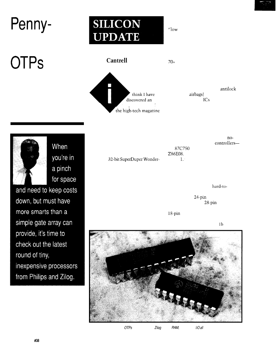
pinching
Tom
unspoken tenet of
business: The amount of breathless
editorial coverage given to any new
widget is inversely proportional to its
relevance in real-world applications.
If you were to judge yourself by
typical trade journal covers, you
would be a Neanderthal (or an incur-
able Luddite) if you chose not to use
the latest
chip.
Well, I just have to say, “Humbug
to that noise!” Sure, these
multimegagate wonderchips are
useful-especially when it comes to
replacing the “big iron” of old. But I’ve
always felt that the biggest benefit of
the silicon revolution is reserved for
the low end. In the final analysis, it
comes down to the difference between
doing something that has already been
done before (albeit less expensively)
versus doing something that has never
been done. This class of unique, new,
end” products is only now
possible because it can finally be done
cheaply enough to make the exercise
worthwhile.
For instance, I recently read that
cars produced today have on average
chips manufactured into them.
Current trends indicate this number
will increase. Admittedly, the main
ECU (Engine Control Unit) is likely to
be a rather high-tech device, but much
of the really neat stuff (like
brakes and
are made possible
by mass-produced
whose main
“feature” is that they are priced low
enough to prevent terminal sticker
shock.
So let’s get some cheap thrills by
taking a look at a couple of popular
penny-pinching OTP (One Time
Programmable, or EPROM in a
window plastic package)
the
from Philips and the Zilog
These devices are shown in
Photo
LESS IS MORE
Starting with packaging, Photo 1
shows you won’t have to fuss with
fragile, high-pin-count,
assemble-with packages. The ‘750 is
available in a
skinny-DIP (0.375
square inches) or a
PLCC (0.25
square inches). The ‘E08 comes in an
DIP (0.28 square inches).
Let’s move inside for an even
closer look. Figures la and show the
Photo l--Penny-pinching
from Philips and
include
PROM, and on one chip.
64
Issue
September 1993
The Computer Applications Journal
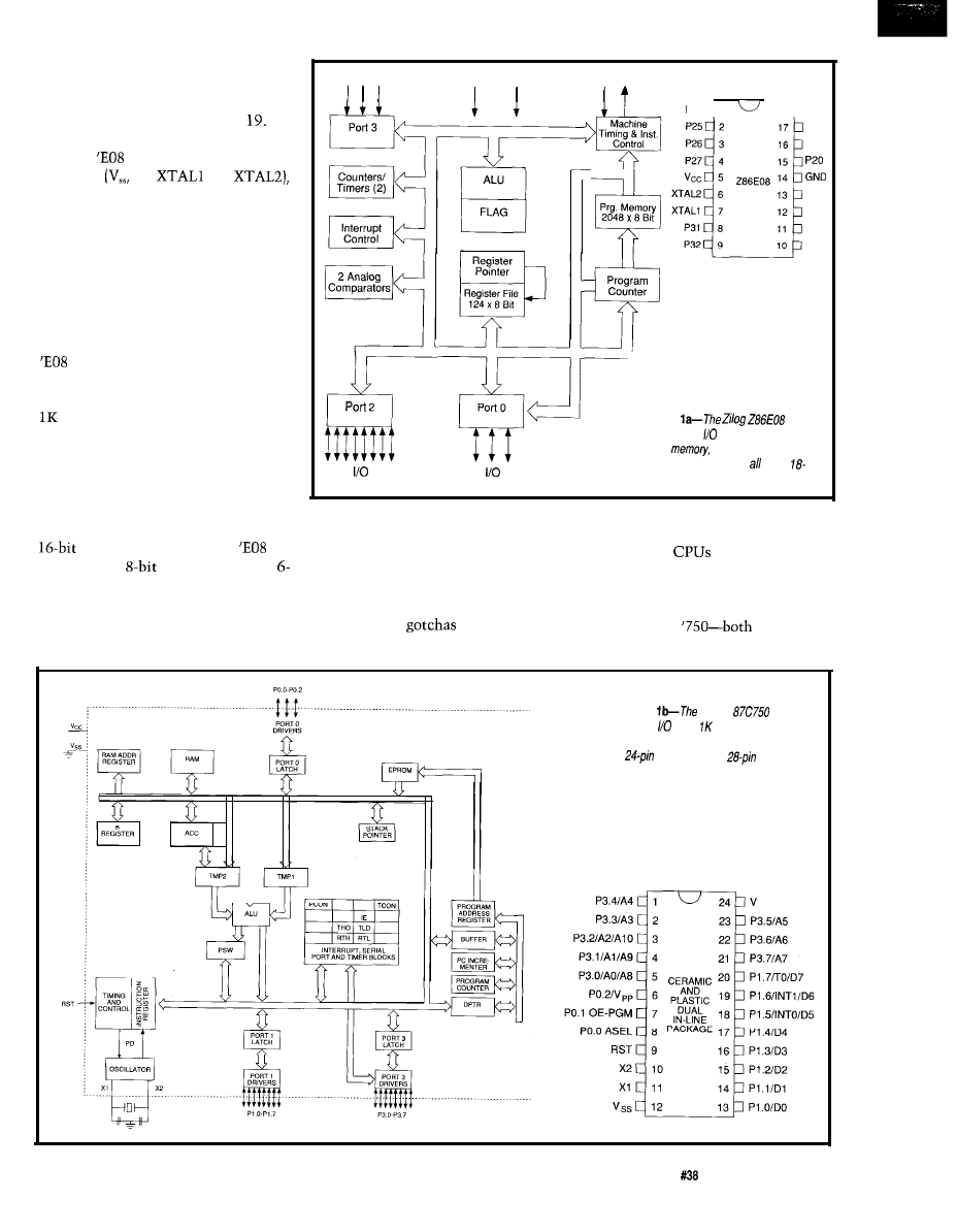
Input
the ‘750 doesn’t use the extra four pins
provided by the package, it still packs
“ c c
GND
XTAL
Prg. Memory
2048 8 Bit
block diagrams of these chips. With
I/O functionality limited by the pin
count, the ‘E08 offers 14 I/O lines
while the ‘750 manages to offer
Keeping efficiency in mind, notice
how the
only needs four lines of
overhead
V,,,
and
while the ‘750 adds a fifth (RST).
Though the 28-pin PLCC version of
P24
1
18
P23
P22
P21
PO2
PO1
PO0
P33
the largest number of I/O lines in the
smallest board space.
Both chips are miserly when it
comes to doling out memory, so put
your C compilers away for now. The
offers a cozy 2K bytes of OTP
memory and 144 bytes of RAM while
the ‘750 is lean-and-mean with only
byte of OTP memory and 64 bytes
2
Port 0
Figure
of RAM.
contains 14 lines, 2K bytes of
Other than this trim offering of
OTP
144
bytes of RAM,
memory, little more than timers and
and a power-on reset, on an
counters are deemed worthy enough to
3it Programable)
pin D/P.
receive any of the scarce transistors on
these chips. The ‘750 provides a single
NOT SO FAST
timer/counter while the
“Not so fast” is also the way to
Since our beloved editor didn’t fall
describe these
so we can avoid
opts for twin
units, each with a
for my little ploy, let’s take a closer
bit prescaler.
long-winded performance analysis and
look at the features of each chip while
Boy, these simple chips sure make
“architecture wars.” At entry-level
keeping a watchful eye out for any
life easy for us writers-see you next
clock speeds-12 MHz for the ‘E08 and
style-crimping
that might be
month.
16 MHz for the
chips
hiding to bite you later.
toddle along at about 0.5-l MIPS.
Figure
Philips
has 19 fines,
byte of OTP
memory, and 64 bytes of RAM in a
skinny-D/P or a
PLCC package
The Computer Applications Journal
Issue
September 1993
6 5
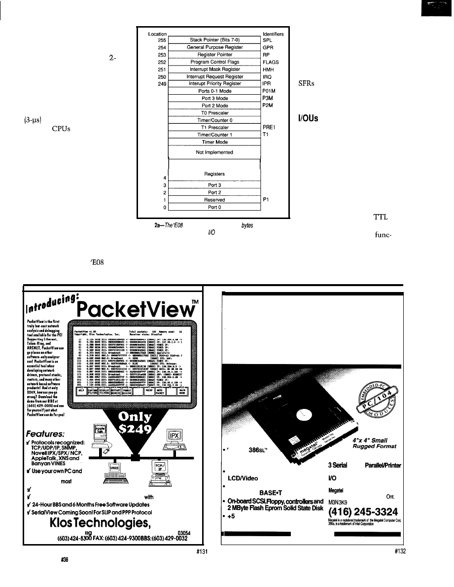
Sure, there are some minor
differences, but nothing worth
quibbling about. The ‘E08 makes
up for a slower clock with a
stage pipeline and a clean
instruction set. On the other
hand, even though the ‘750
suffers from accumulator con-
striction disease (bottleneckitis),
it does feature some pretty fast
multiplies and divides.
Both
utilize separate
code and data spaces, with special
instructions
(M 0 V C for the ‘750
and
LDC for the ‘E08) for reading
data from the program space
(useful for lookup tables, con-
stants, etc.). I suspect code
density for the two chips is
similar, averaging something less
than 2 bytes/instruction. This
limits program size to around 500
lines for the ‘750, and 1000 lines
for the ‘E08.
Figure
RAM layout dedicates 124
to genera/-
purpose
registers and the rest to and control-related functions.
Figures 2a and 2b show the
respective memory maps for the ‘E08
and ‘750. Though the
data sheet
trumpets 144 bytes of RAM, only 124
246
247
246
245
244
243
242
241
127
PREO
T O
TMR
General Purpose
P3
P2
PO
the ‘75O’is divided into four
banks of eight registers, 16 bytes
of bit- or byte-addressable RAM,
and 16 bytes of regular (i.e., byte
addressable only) RAM. The
dozen or so ‘750 I/O and control
(Special Function Registers)
aren’t counted as part of the 64
bytes.
The nineteen I/O lines of the
‘750 are divided into one %-bit
port (port 0), and two 8-bit ports
(ports 1 and 2). I’ll award them
extra brownie points for the fact
that every pin on every port is
individually definable as being an
input or output. Each of the pins
of port 0 is distinguished with
open-collector drivers while the
pins of ports 1 and 2 are
compatible, and include internal
pull-ups. If the alternate
bytes can be used for general purposes.
tions (*INTO and
l
INTl) or the timer
The rest of the space is dedicated to
input (TO) are used, then the width of
I/O and control-related functions.
port 1 is reduced since each of these
Meanwhile, the 64-byte RAM space of
requires a bit from port 1.
Ethernet network
adapter (in
cases)
Programmable Filtersfor
Captureand
Display
Custom Protocol Decoders can be developed
C or Assembler
Analysis
Inc.
604 Daniel Webster Hi
Voice:
hway, Merrimack, New Hampshire
Embedded
P C
with on-board
Ethernet
and
Super VGA
25 MHz
CPU; including up
Other features include:
to 18 MByte DRAM
Porte,
On-board Super VGA
port, BIOS, Real lime Clock,
controller
Bus Expansion
On-board Ethernet, Featuring
For more information call:
AUI and 10
interfaces
Computer Corporation
125
Wendell Ave., Weston,
Fax: (416) 245-6505
volt only operation,
5
watts power consumption
megatel”
66
Issue September 1993
The Computer Applications Journal
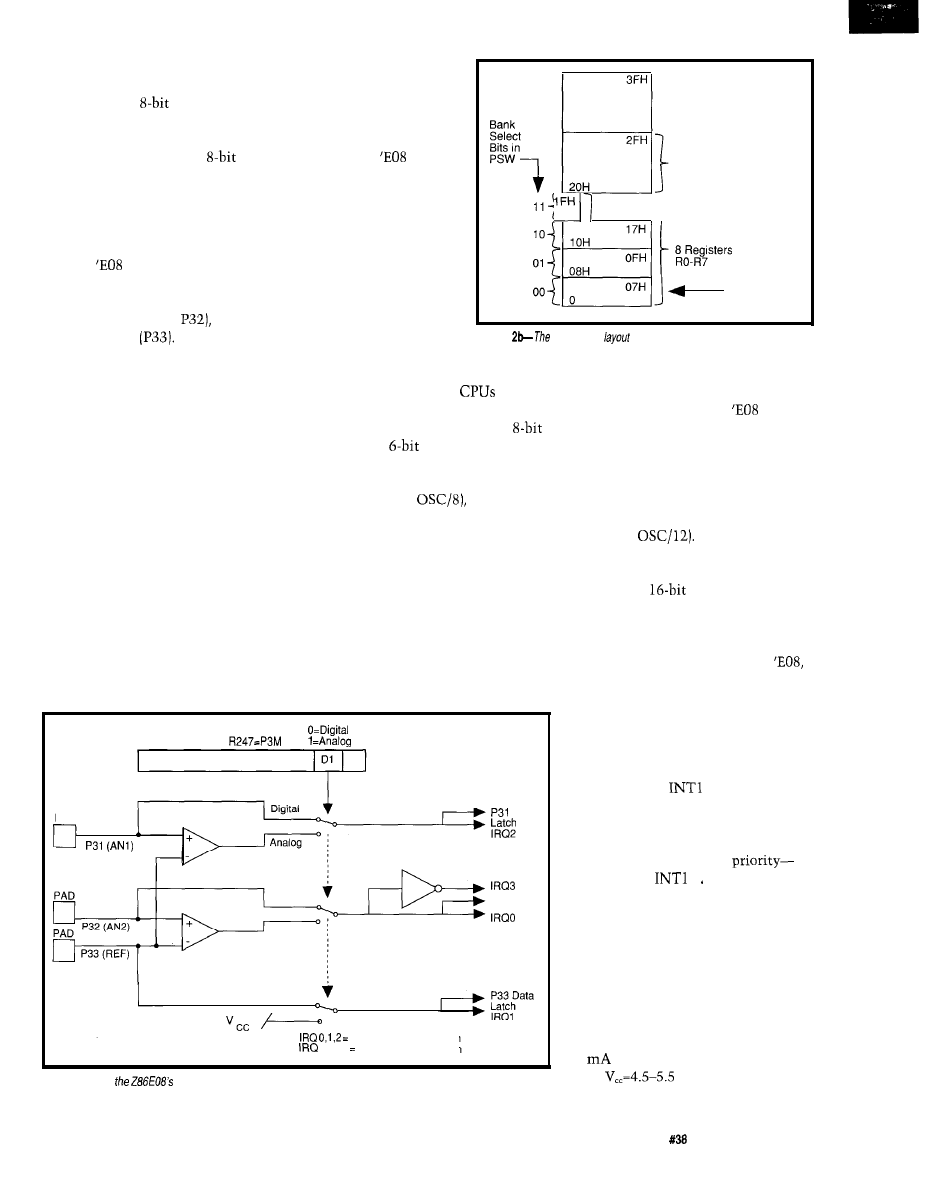
The 14 I/O lines of the ‘E08 are
allocated to a pair of 3-bit ports (ports
0 and 3) and an
port (port 2).
Notice that this part has no port 1.
This device is more restrictive than
the ‘750, because only the
port
(port 2) has bit-programmable pins that
can be used as input or output. Port 0
is globally (all three bits together)
programmable as input or output. Port
3 is hard wired as input only.
The
does manage to sneak in
an extra feature [shown in Figure 3).
Port 3 of the ‘E08 offers two analog
comparators (P3 1 and
and a
both of these chips use
CMOS drivers/receiv-
ers. Generally, the
devices are TTL
compatible, though it
appears the
needs
pull-ups on inputs
driven by TTL.
PART TIMERS
Though it’s a little
more cramped on the
I/O front, the ‘E08 does
pull ahead slightly
because it offers two
Bit-Addressable Space
(Bit Addresses 0-7F)
4 Banks of
R e s e t V a l u e o f
Stack Pointer
reference input
However, these
timers as opposed to the
Figure
‘750 RAM
shows four banks of eight registers and 16
same pins can also function as the
‘750’s single timer unit.
bytes of bit-addressable RAM.
pin 1 of port 3 can be used for the
external interrupt inputs (IRQO-IRQ3).
optional (and only) external timer
Unfortunately, the analog or digital
input. This is the case whether the
port is configured as an analog or a
function can only be selected for the
digital port. Finally, bit 7 of port 2
serves double duty as an optional input
that can be used to bring the CPU out
entire port and not on a bit-by-bit
of STOP (low power) mode.
basis. Though not shown in the figure,
One note of caution-make sure
to check the drive capacity levels of
any I/O pin to verify compatibility
with whatever you’re connecting it to.
This is especially important, since
resolution of
14
bits. The input clock
is derived from the crystal frequency
Otherwise, the timing and counting
[the clock runs at
so its range
is from 666 ns to 10.9 ms. From the
capabilities of these two
are
figure you can see that timer I can
optionally utilize one of the bits of
quite similar.
port 3 as an external clock input. This
bit can also serve as a gate/trigger for
The ‘E08 (Figure 4a) features
the internal clock. Each timer has
initial value registers that can option-
counters and
prescalers for a total
ally be called into play for automatic
reload. Each timer can generate an
interrupt which (when considered
PAD
P32 Data
Latch
Falling Edge Detection
Rising Edge Detection
Figure 3-One
of
unique
features is a pair of analog comparators. The analog inputs share pins with
the regular digital pork and interrupt inputs.
along with the four possible external
inputs) brings the total number of
interrupts handled by the
to six.
The timer in a ‘750 (Figure 4b) is
basically the same as an 805 1 timer
operating in mode 2 (automatic
reload], except its resolution is
extended to 16 bits. This clock is also
derived from the crystal (it ticks away
at a rate of
The resolution of
this timer (750 ns) is slightly lower
than the resolution of the timer in the
‘E08, but the
range of the ‘750
extends all the way up to 49.2 ms. Like
the ‘E08, the ‘750 can sacrifice an I/O
line (bit 7 of port 1) for use as an
external timer input. Unlike the
gating external signals uses a second
pin of the port. The good news is that
this allows gating of an external timer
input, something the ‘E08 can’t do.
The bad news is that the line used for
gating is the same one used by INTO’,
leaving a lonely
l
as the only
external interrupt source. By the way,
the ‘750 abandons the 805 l’s two-level
programmable interrupt priority
scheme in favor of a fixed
INTO * , timer,
l
GREEN MACHINES
One of the primary methods of
economizing in embedded systems is
the reduction of power consumption.
Both of these chips are positively
Scrooge-like when it comes to running
up the electric bill.
The ‘750 typically consumes only
12
when it is running at 16 MHz
(with
V) and, as usual for
CMOS, the power consumption
The Computer Applications Journal
Issue
September 1993
6 7
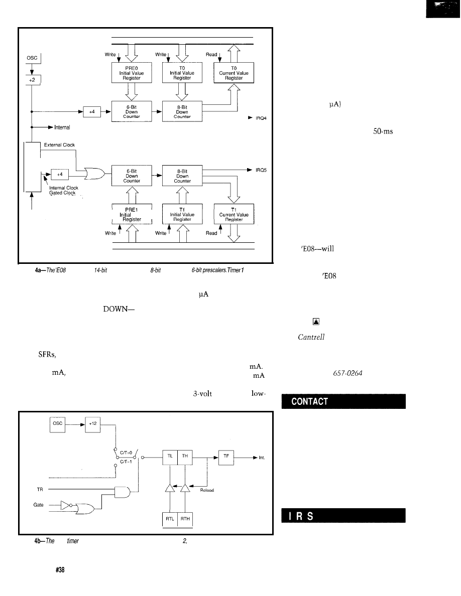
Clock
Clock
Logic
IN P31
Internal Data Bus
Triggered Clock
Value
Internal Data Bus
Figure
timers
have
resolution by using
counters and
can a/so use
an external clock
input.
declines linearly with the clock rate.
Philips has added their own low-power
maximum of
50
and preserving
modes-IDLE and POWER
only on-chip RAM. POWER DOWN is
to the ‘51 architecture. IDLE mode
only recoverable through a reset.
defines a semiawake state in which all
The ‘E08 is even more power
CPU activities stop, but the state of all
conscious and, much to its favor, it is
other peripherals on the chip (I/O,
specified to operate at both 3 and 5
volts. Even when this device is
RAM,
etc.) remain intact. Power
consumption during IDLE mode is
running at 12 MHz and powered by 5
typically 2
and waking up the
volts, its active I,, is typically 9
chip is quick and easy in response to
Power consumption drops to 3.6
at
any enabled interrupt. POWER DOWN
this clock speed when the chip is
mode is comatose indeed, consuming a
powered by a
supply. The
power modes of the ‘E08 (HALT and
TO Pin
INTO Pin
R T L R T H
Figure
‘750
is basically the same as an 8051 timer in mode but ifs resolution is extended to 16
bits.
STOP) function very much like the
IDLE and POWER DOWN modes of
the ‘750. However, the ‘E08 does offer
you the choice of using a port bit (bit 7
of port 2) for STOP mode recovery.
This has fewer side effects (such as
initializing I/O) than a recovery by
reset, and makes using the lowest
power (only 10
mode easier.
The ‘E08 racks up a few more
points by integrating a power-on reset
delay (no reset pin needed), a
watchdog timer (which can be enabled
or disabled during low-power HALT
mode), and built-in, low-voltage
(“brownout”) protection. The ‘E08
even includes a low EM1 mode in
which output power and slew rate are
reduced to minimize RF pollution.
PRICE IS RIGHT
Likely as not, one feature or
another-such as the hardware math
of the ‘750 or the brownout protection
of the
prove to be the
compelling factor for certain applica-
tions. Whichever chip you choose, at
$3.50 for the
and $4.50 for the
‘750 (lk, plastic DIP, 0-70°C) you’re
getting a lot of micro for your money.
And at this low cost, you can afford to
lash one of these devices to almost
anything.
Tom
has been an engineer in
Silicon Valley for more than ten years
working on chip, board, and systems
design and marketing. He can be
reached at (510)
or by fax at
(510) 657-5441.
Philips Semiconductors
811 East Arques Ave.
P.O. Box 3409
Sunnyvale, CA 94088-3409
(408) 991-3737
Zilog, Inc.
2 10 Hacienda Ave.
Campbell, CA 95008-6609
(408) 370-8000
416
Very Useful
417 Moderately Useful
418 Not Useful
68
Issue
September 1993
The Computer Applications Journal
Sonar Ranging Experimenter’s Kit
EEG Biofeedback Brainwave Analyzer
Targeting Ranging Machine Vision
The HAL-4 kit is a complete
The Circuit Cellar
Ultrasonic Sonar Ranger is based on the
electroencephalograph
which
sonar ranging circuitry from the Polaroid SX-70 camera system. The
and the original SX-70 have similar performance but the
Sonar
measures a mere
HAL is sensitive enough
to even distinguish different conscious
Ranger requires far less support circuitry and interface hardware.
The
ranging kit consists of a Polaroid
300-V
between concentrated mental activity and
ant daydreaming. HAL gathers all
alpha,
static transducer and ultrasonic ranging electronics board made by Texas
Instruments. Sonar Ranger measures ranges of 1.2 inches to 35 feet, has a
beta, and theta brainwave
signals within the range of
TTL output when operated on
and easily connects to a parallel
printer port.
4-20 Hz and presents it in a
serial digitized format that
Sonar Ranger kit.
. . . . . . . . . $79.00
plus shipping
HAL’s operation is
CHECK OUT THE NEW CIRCUIT CELLAR
‘four
of analog brainwave data 64
times per second and transmits this digitized data serially to a PC at 4800
HOME CONTROL SYSTEM
bps. There, using a Fast Fourier Transform to determine frequency,
amplitude, and phase components, the results are graphically displayed
in real time for each side of the brain.
Expandable Network
Trainable IR Interface
Digital
and Analog I/O
Remote Displays
X-10 Interface
HAL-4 kit
plus shipping
Call and ask about the HCS
The
Cellar Hemispheric Activation Level detector presented as an
example of the
used
Level detector is
a
approved
no medical
are made for
and should not be used for
medical
purposes. Furthermore, safe use
that HAL be battery operated only!
To order the products shown or to receive a catalog,
call: (203) 875-2751 or fax: (203) 872-2204
Circuit Cellar Kits
l
4 Park Street
l
Suite 12
l
Vernon, CT 06066
We're
Powerful,
ALSO AVAILABLE:
In fact, you’ll get the best product for about
half the price. If you’re interested in getting the
most out of your project, put the most into it.
For the least amount of money.
Call us today for complete data sheets, CPU
options, prices and availabilitv.
Work
Welcome. Call or fax for
complete data sheets
2308
East Sixth Street
bookings, SD
57006
Phone (605) 697-8521
Fax (605) 697-8109
The Computer Applications Journal
Issue
September 1993
6 9

Storage for
the Masses
John Dybowski
0
he term “mass
storage” means
different things to
different people. Most
computer-literate persons agree that it
applies to some form of
byte storage space. However, “mass
storage” is different for many develop-
ers of embedded systems because these
folks play in a different arena.
Most embedded systems are based
on
controllers that don’t have the
capability to access significant
amounts of memory. Even a 16-bit
controller (such as an 80186) uses
than-optimal methods to access
megabytes of address space. Even this
processor uses an architecture that is
little more than a stylized paging
scheme. Segmented memory architec-
tures present enough headaches. If you
add a banked memory scheme to this
kind of system, you simply compound
the problems associated with a
segmented memory.
At first glance, a megabyte may
seem like a lot of memory. But there
are circumstances associated with the
design tools used for 16-bit controllers
that tend to nibble away at it. For
instance, the development environ-
ments adopted for larger controllers
often use compiled languages. Pro-
grams developed using these methods
seem to have an inordinate hunger for
substantial amounts memory.
Often, the memory space must be
broken up to accommodate various
families of memory components such
as PROM
S
,
and flash devices.
Any of these components may not be
fully utilized, which even further
reduces the available space. Large
controllers often need memory
expansion tricks as much as their
smaller siblings.
There is an opposing force in
embedded systems design. This force
is the necessity to contain costs. This
compulsion usually means that
designs are done with cheap control-
lers. As a result, it is not uncommon
to find instruments that use a $2.00
processor to drive $50.00 worth of
memory. The situation is eased when
the controller has a conventional
parallel bus. This is especially true
when on-chip I/O can handle the bank
switching. Things get sticky when you
try to pull it off with controllers that
have very little I/O. As luck would
have it, IC manufacturers come to the
rescue and provide packaged answers
to these concerns.
Now that the problem is under-
stood, I’ll describe ways to solve it.
First I’ll present a conventional
switching scheme that works with a
standard bus architecture. Then I’ll
show you a way that operates using
just three wires and can be adapted to
a variety of controllers.
MEMORY BANKS
Banked memory schemes are
structured in various ways. You can
map memory into the I/O space (for
processors having separate I/O instruc-
tions) or you can design banked RAM
into the conventional memory space.
The idea is to designate an address
range as a memory page where differ-
ent sections of physical memory can
be swapped. Bank selection is usually
done by manipulating signal lines that
are used as an “address” by bank
decoders.
The page size is made as large as
possible to minimize how often bank
changes must be done. I’m a big fan of
dumb code anyway, and resist the
temptation to make the code do any
more than absolutely necessary.
Circumstances sometimes change, so
the trick is to avoid coding yourself
into a corner. Although some mali-
cious programmers take great delight
in contriving diabolically complex
sequences,
I
prefer to’allow code to
function in a simple and mechanical
manner unless there is some compel-
ling reason to do otherwise. If code is
70
Issue
September 1993
The Computer Applications Journal
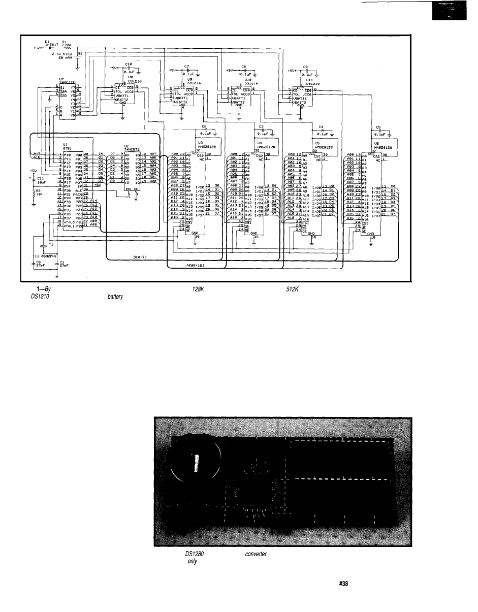
Figure
using a
pair of output port bits, it’s possible to select one of four
banks
of memory, allowing a total of
of memory on an 803 l-based system.
The
chips manage the backup
which protects the RAM chips’ contents.
written properly, it’s usually easy to
add intelligence in upper layers if you
have to be clever. In any case, making
the bank size as large as possible helps.
An arrangement can be devised
where several addresses are designated
as address and data registers. The
address registers describe the location
to be accessed, and the size of the page
is the size of the controller’s data bus.
This extreme situation does have the
advantage of using only a few address
locations. The disadvantage is you
must explicitly set up the entire
address for each access. The method
you use depends on the processor, the
way the system operates, and, most
importantly, the way the data is used.
If all you need to develop is a large
buffer, or a circular queue, then you
can take some license. If frequent
random accesses are needed then the
setup may be more restrictive.
BANKING ON THE 8031
Using the 803 1 to manage signifi-
cant amounts of memory exemplifies
the challenge of embedded instrument
controllers go when you consider its
design. The problem with the 8031 is
ability to access 64K of program
not its limited memory accessing
memory and 64K of data memory. Its
internal RAM, special function
registers, and bit region offer several
capability. It’s really not bad as
useful kinds of storage. The problem
with the 8031 is that it is a “basic
implementation” of a single-chip
8031 is flourishing after fifteen years of
microcontroller and has serious
service. New derivatives are being
introduced regularly.
restrictions in its external memory
addressing modes. In spite of this, the
Although there are negatives, the
8031 does help you implement a
banked memory system. One problem
associated with bank switching is
maintaining a section of RAM that is
Photo l--The
serial-to-bytewide
can be used as the core of a serial-based memory module. Note
that the chip is
available in a quad f/at pack package.
The Computer Applications Journal
Issue
September 1993
7 1
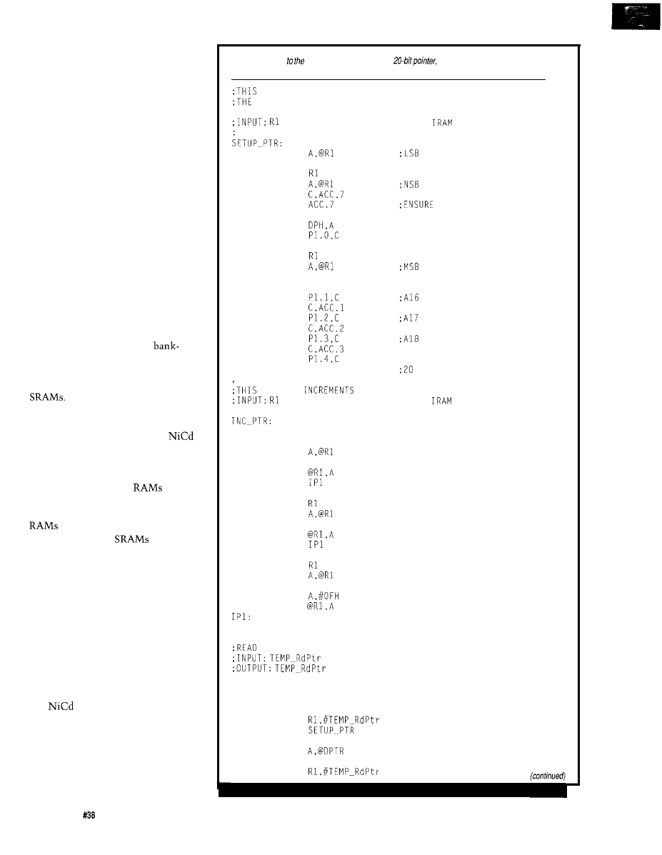
always available regardless of which
bank is in service. An example of this
requirement is the system RAM. The
stack region, general-purpose buffers,
and data areas required by interrupt
service routines should always be
active. If the system RAM were
switched out when an interrupt
occurred, mayhem would result. The
other concern is the I/O required to
perform bank switching. The I/O must
be available regardless of which bank
is active. It helps if this I/O is easily
accessible to reduce the overhead of
bank manipulations.
These problems can be circum-
vented with the 8031 since the stack is
in internal RAM, and you might find
enough internal RAM left over to
satisfy the system’s general purpose
storage needs. The on-chip addressable
I/O offers a way to access the pins to
do the bank switching.
Now I’ll demonstrate a
switching arrangement with the 803 1.
Referring to Figure 1, you will see the
memory system consists of four 128K
The decoding is done by a
‘138 operating under firmware control
via several on-chip I/O pins. Each
RAM is battery backed using a
battery composed of two cells and a
Dallas Semiconductor DS1210 RAM
controller. This arrangement provides
a good match for these
since the
end-of-discharge voltage is 2 volts.
This is the minimum voltage the
require for data retention.
Remember, CMOS
draw less
current given a lower standby voltage,
so it makes sense to keep the backup
voltage low.
An important consideration in
using RAM controllers with recharge-
able batteries is the high end of the
battery voltage. This voltage cannot
exceed the VCC power-fail trip point
or the part will never go into backup.
Since the DS 12 10 is. designed to run off
a lithium cell, the maximum battery
voltage restriction makes sense. With
two
cells this is not a problem
since the battery will never exceed 3
volts even when the cells are held in
overcharge. With three cells you could
be playing with fire.
The RAM area is partitioned into
32 pages. Each page is 32K deep and is
Listing l--Access banked region is
through a
which is supported using several
routines.
ROUTINE TRANSLATES THE 20 BIT LOGICAL ADDRESS TO WHAT
HARDWARE REQUIRES TO ACCESS THE BULK RAM AREA.
POINTS TO 20 BIT POINTER IN
MOV
MOV
INC
MOV
MOV
SETB
DPL,A
MOV
MOV
INC
MOV
MOV
MOV
MOV
MOV
MOV
MOV
MOV
MOV
RET
C,ACC.O
ROUTINE
THE 20 BIT LOGICAL POINTER.
EXTERNAL ACCESS
;A15
;A19
BIT ADDRESS IS SET
POINTS TO 20 BIT POINTER IN
PUSH
ACC
MOV
INC A
MOV
JNZ
INC
MOV
INC A
MOV
JNZ
INC
MOV
INC A
ANL
MOV
POP
ACC
RET
A BYTE FROM THE BULK RAM AREA
POINTS TO NEXT BYTE TO READ
IS INDEXED TO NEXT LOCATION
G
E T
-
BYTE
:
PUSH
DPL
PUSH
DPH
MOV
CALL
MOVX
MOV
7 2
Issue
September 1993
The Computer Applications Journal
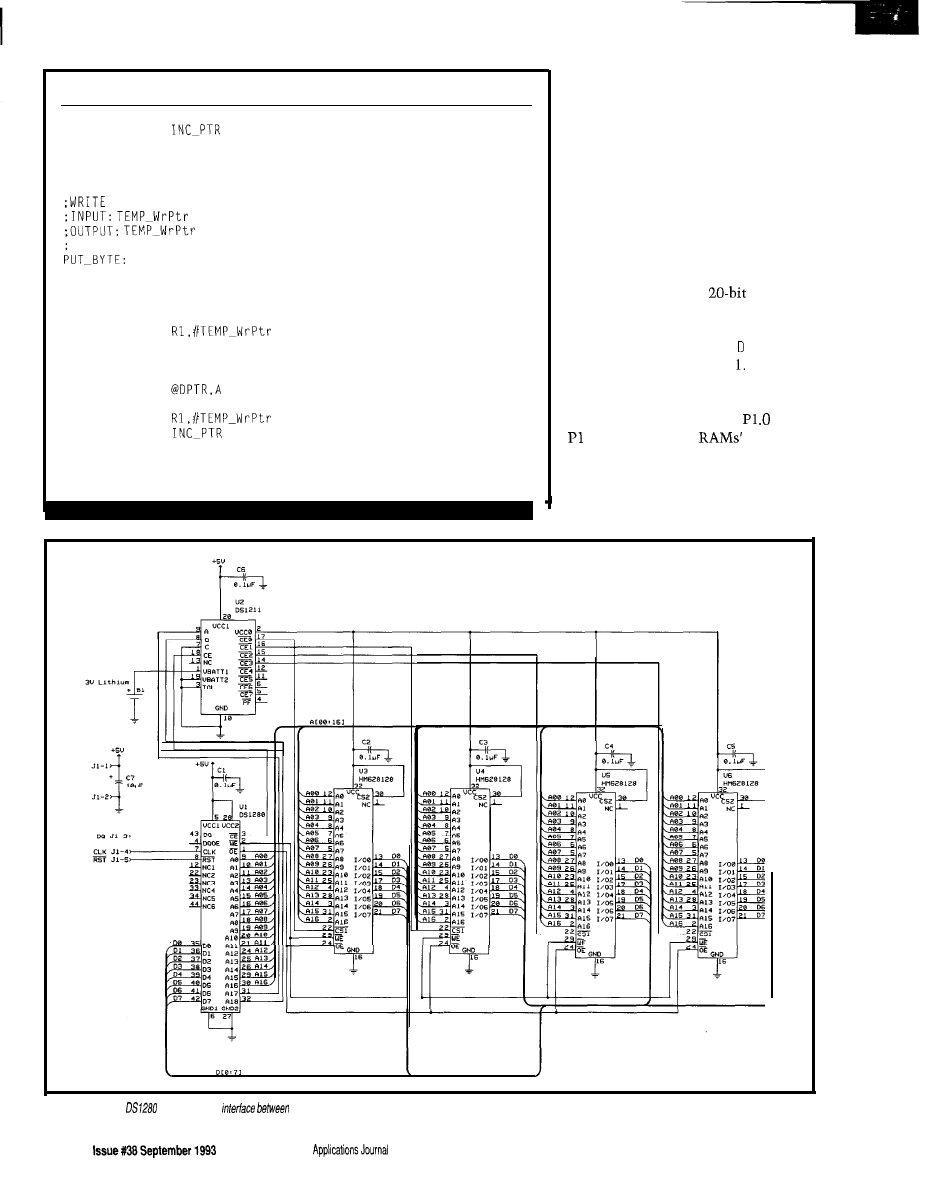
Listing l-continued
CALL
POP
DPH
POP
DPL
RET
A BYTE TO THE BULK RAM AREA
POINTS TO NEXT STORAGE LOCATION
IS INDEXED TO NEXT LOCATION
PUSH
DPL
PUSH
DPH
PUSH
ACC
MOV
CALL
SETUP_PTR
POP
ACC
MOVX
MOV
CALL
POP
DPH
POP
DPL
RET
located in the upper half of the data
address space. This leaves the lower
32K available for a system area and
general-purpose storage. The lower
RAM can also be nonvolatile and can
be used to hold control information
and other variables necessary to
operate the bank-switched area. With
the 8031’s separate program area, a full
64K of program memory is still
available so you can write lazy code.
Access to the banked region is
through a synthesized
pointer
that is passed through a setup routine.
Referring to Listing 1, you can see the
lower 15 bits are placed into PTR and
the high-order bit is set to This is
done to displace the transfer region to
the upper 32K of the address range.
Bits 15 and 16 are moved to and
.l
which drive the
address
lines with the remaining three address
bits presented to the ‘138 via P1.2,
P1.3, and P1.4. Following this, the data
transfer into or out of the RAM is
r
Figure P-The
provides a clean
a simple three-wire serial interface and the mass of wires and connections associated with a large memory array.
74
The Computer
handled by second-level functions that
execute a standard MO V X instruction.
Although the logical address is a
contiguous span that goes from
to
the transfers occur at
physical addresses that range from
8000h to
Also in Listing 1 are several
support routines. Writing such
constricted routines is more than an
exercise in small thinking; the desired
result is the flexibility such noncom-
mittal function blocks offer. I used
these basic services to craft a circular
queue in a straightforward manner
using conventional coding techniques.
SERIAL RAM
Effective as bank-switched RAM
is, there are times when it pays to do
the job with just a few wires. Reducing
the interconnect burden is appealing
when the RAM is on a separate card,
where the reliability and cost of every
connection is a prime concern, or
when your controller does not have a
bus architecture to begin with. In any
case, serial interfaces are interesting
and the throughput is often adequate.
Contriving a serial RAM interface
from scratch would involve a prohibi-
tive amount of logic or the use of a
dedicated microcontroller with its
inevitable speed penalty. Due to the
complexity involved in engineering a
reliable serial interface, the end result
would likely prove disappointing.
I
found a part that seemed like the
answer to these problems. It took a
little longer than I expected to get
from here to there, though.
STEALTHSPECSHEETS
The Dallas DS1280
converter looked like it
would handle the serial conversion.
Using a three-wire serial interface
composed of a reset
a clock
(CLK), and a bidirectional data (DQ)
line, this is an example of another
proprietary interface. I’m not a big fan
of proprietary interfaces, but under the
circumstances there’s really not that
much to complain about.
One interesting amenity in the
DS1280 is a built-in CRC generator. In
addition to checking the validity of
commands, it can also be used by the
CALL OR FAX TODAY FOR
MORE INFORMATION ON
OUR COMPLETE LINE OF
Technical
EPROM EMULATORS,
PROGRAMMERS AND
ACCESSORIES1
PO BOX 462101
GARLAND, TX
NEWFAXNUMBER: (214) 494-5814
Frame Grabber
l
$495 Including Software with
Libra
l
Half
Card for Compact Applications
l
Real Time Imaging with Display Output
l
8 Bit (256 Gray Levels)
The Computer Applications Journal
Issue
September 1993
7 5
system controller to verify the data
stream is written and read correctly.
The inclusion of this safeguard should
not be surprising since the DS1280 is
the converter chip used in Dallas’s
cartridges. In this applica-
tion, the CRC is an important compo-
nent that guards against interconnec-
tion errors due to intermittent con-
tacts. It can also trap on errors when
the cartridge is inserted and removed. I
was ready to wire up my memory stick
when I realized the DS1280 must be
used primarily used by Dallas inter-
nally in its memory cartridge products.
This realization came upon me after a
cursory examination of the data sheet.
With the problems I had figuring this
part out,
I
came to the inescapable
conclusion that nobody else could
possibly be using it!
As they say, if you’re going to
screw something up, you might as well
do a job of it. Since the DS1280 is only
available in a quad flat pack (which
meant hand wiring would be quite a
chore], naturally one of my first
concerns was in not making any
Listing
memory interface is
by three routines.
the DS1280 controller and interface pins
the I/O pins to their idle state
the select bits to
setb CLK
setb
clr RST
default clock level
default data level
reset
read current (random) select bits
mov
CRC value
setb RST
reset
mov
call XByte
read function
mov
dummy address
call XByte
address bits
mov
call XByte
;mid address bits
mov
addr and read command
call XByte
mov
dummy select bits, CRC
call XByte
select bits
mov
call XByte
select bits
mov
a,CRC
call XByte
CRC value
(continued)
Memory mapped variables
In-line assembly language
option
Compile time switch to select
or
Compatible with any RAM
or ROM memory mapping
Runs up to 50 times faster than
the MCS BASIC-52 interpreter.
n
Includes Binary Technology’s
cross-assembler
hex file
n
Extensive documentation
n
Tutorial included
n
Runs on
or
Compatible with all 8051 variants
n
508-369-9556
FAX 508-369-9549
Binary Technology, Inc.
P.O. Box 541
l
Carlisle, MA 01741
MOVE OVER INTEL
MICROMINT SOURCES
CMOS BASIC CHIP
Micromint has a more efficient software-compatible
successor to the power-hungry Intel
chip. The
chip was designed for indus-
trial use and operates beyond the limits of standard
commercial-grade chips. Micromint’s
chip is guaranteed to operate flawlessly at DC to
12 MHz over the entire industrial temperature range
(-40°C to
Available in
DIP or PLCC
chip
$25.00
OEM
Price
$14.50
BASIC-52 Prog. manual
$15.00
MICROMINT, INC.
7 6
Issue
September 1993
The Computer Applications Journal
Listing
2-continued
get the current select bits and save
call
low select bits
push
call
high select bits
push
clr RST
is complete
set the select bits to a known state
setb RST
reset
mov
call XByte
write function
mov
dummy address
call XByte
address bits
mov
call XByte
address bits
mov
addr bi, write select cmd
call XByte
current select bits snd CRC
b
high select bits
pop
low select bits
call XByte
mov
call XByte
mov
call XByte
CRC value
mov
the new select bits
call XByte
select bits
(continued)
wiring errors that would let the magic
smoke out of the chip. My fears were
not unfounded. Luckily, it didn’t take
me long to find out that there were
problems with the
sheet. The fact
that a 44-pin quad flat pack has 11 pins
on a side and the data sheet’s diagram
showed the nomenclature for 12 pin
designations on one side was a dead
giveaway. How’s that for security
against unauthorized use? After
several calls to the factory, I had the
correct
but
I
must confess, my
confidence was a shaken since there
were other errors in the data sheet as
well. Anyway, I’m happy to report I
was able to get it working without
blowing it up.
Referring to Figure 2, you can see
how I devised a memory system
around the DS1280. The DS1280 has a
three-wire interface on the processor
side and a standard address and data
bus on the memory side. This memory
interface provides the capacity of
driving up to
of memory through
19 address lines, 8 bidirectional data
lines, and an active-low chip select.
We offer a full line of low cost
embedded
controllers and software tools which are ideal for
developing products, test fixtures and prototypes.
Features Include:
l
Low
Up
dataspace
15 volt operation
Small
form factor(3.5"
prototyping area
System diskette includes
notes
Available Options:
Multifunction Board adds A/D, 24 lines and more!
BASIC-52 or
EPROM,
C
$300
Iota Systems, Inc.
POB 8987
l
Incline Village, NV 89452
PH: 702-831-6302
l
FAX: 702 831-4629
See us Embedded Systems
The Computer Applications Journal
77
This chip also has a control signal
(DQOE) that can enable a tristate
driver when the DS 1280 is emitting
data.
Nonvolatility is attained by using
a Dallas DS1211
decoder/
nonvolatizer IC and a lithium cell. The
two high-order address lines feed the
DS1211, which select one of the four
RAM chips. The
chip select
signal is an enable strobe to the
DS 1211. The use of the enable ensures
that all of the
remain disabled,
in a quiescent state, if a RAM access is
not taking place. This keeps power
consumption down. The remaining
address lines are brought out to the
RAM chips as are the data lines. Photo
1 is a picture of the result of my labors.
Notice that this prototype has only
two RAM chips for a total of 256K of
storage-enough to prove the point.
SERIAL GYRATIONS
The DS1280 uses a
com-
mand sequence (including CRC) to
initiate any action. Following the
successful transfer of a command
Listing
2-continued
mov
call XByte
select bits
clr RST
is complete
ret
burst write to RAM via
19 bit address is in
is
dptr points to source buffer
contains byte count
if write CRC is ok
mov
if nothing to write
mov
CRC value
setb RST
reset
mov
call XByte
write function
mov
address
call XByte
address bits
mov
cal
mov
cal
mov
cal
mov
a,r3
XByte
;mid address bits
address bits
burst write command
XByte
select bits
XByte
select bits
Project Part5
are
any
(65 pages 3.5’
$18115
to the
Instruction Set (46 pages)
$1018
$312
8255 Cheat Sheet Reference Card
Embedded
Parts (INK
45.70
LED
2.10
Effect sensor
2.25
controller
for
laser)
2.30
laser
controller
laser)
2.85
4.00
Power amp
to
supply, 3 5 A output)
4
38
480
Dual full
stepper motor
45
See
article, INK 29)
Excellent
(opaque to
35 mm
mount)
75
6
watchdog
6
8 latched
6
8 latched 250
7
stepper motor
S-ART
8.10
Number (2
8.40
power
9.75
9.90
red LED.
10.40
MAX691 Power
85
12.00
DTMF
IL300
MAX233
powered
interface
MT8880 DTMF
power
2000
33
MAX252
RS-232
64
UPS
day/Next day
to 48 US states, COD add $4.50. Canada $6 via USPS Air
Small Packet, no
Check, MO, COD only, no credit cards.
add $50, but call
NC residents add 6% sales
discounts
at five parts. Data Sheets Included.
Call/write/fax for serious/y tempting catalog...
Pure Unobtainium
Your
unusual parts
source4
1310901d
FAX/voice
Everybody’s using
.
How do
get started?
HERE!
BASED ON THE POWERFUL AND EASY TO PROGRAM
ADSP-2111 DSP. CONTROL RESOURCES PC-21 11 NOW MAKES IT
EASIER THAT EVER TO BRING SPEECH TO YOUR PRODUCTS.
COMPLETE HARDWARE The PC-21 11
a 12 MHz 2111 DSP.
Program RAM, SK Data RAM. Microphone and Speaker Amplifiers
II
Expansion Port. It can also be used
the PC with only a 5V power
. .
COMPLETE SOFTWARE Included software allows
to
a
An
framework and
speech recognition and
speech compression code are also included. The ADSP-2111
Assembler/Linker/Simulator can optionally be
with
the card.
A COMPLETE SOLUTION In short, the PC-21 11 gives you
you need to get an
on your
DSP
If you still don’t
whereto start,
Control Resources can quote on writing algorithms
or designing custom hardware for your
write
for more information!
Control
Resources
19042 San Jose Ave. Unit P.O.
8694, Rowland
CA 91748
912.5722 (VOICE)
(FAX)
78
Issue September 1993
The Computer Applications Journal
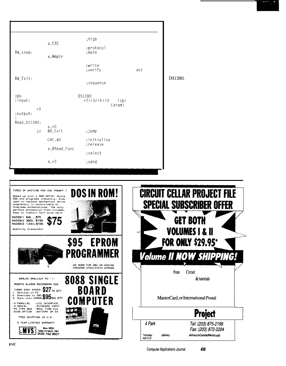
Listing
P-continued
call XByte
select bits
mov
call XByte
CRC value
data write loop
movx
inc dptr
call XByte
data byte
djnz rO.BW_Loop
CRC, result in
call Check-CRC
clr RST
is complete
ret
burst read from RAM via
19 bit address is in
is
dptr points to destination buffer
contains byte count
ACC=O if read CRC is ok
mov
if nothing to read
mov
CRC value
setb RST
reset
mov
call XByte
read function
mov
address
(continued)
sequence, you can perform burst (with
automatic address incrementing) reads
and writes to the RAM, read/writes of
select bits, and reading the internal
CRC register. Let me say a few words
about the hardware signaling at the bit
level before moving along.
A transition of RST from low to
high clears the internal CRC register
and enables communications for the
Dropping RST terminates any
communications operation.
Data is clocked into the DS1280
on the rising edge of the CLK line, and
data is clocked out of the DS1280 on
the rising edge of the CLK line. All
transfers are in octets with the LSB
first, MSB last.
The actual communications
protocol consists of several steps. The
first byte sets up the general operation
(i.e., read or write). The next three
bytes are the address for the RA
M
operation and are transferred with the
LSB first. They can be set to any value
(usually 0) if the operation is not a
RAM access. Only three bits of the
high-order byte contain address
TOP
projects
the
Cellar Design Contest
NEW
projects
Something for every interest
Order both volumes and save!
(regularly $17.95” each)
VISA,
Money
Order (U.S. funds drawn on U.S. bank only)
Circuit Cellar
File
Street
Vernon, CT06066
domestic
Please add $2 for
$4 for other
addresses
The
issue
September 1993
79
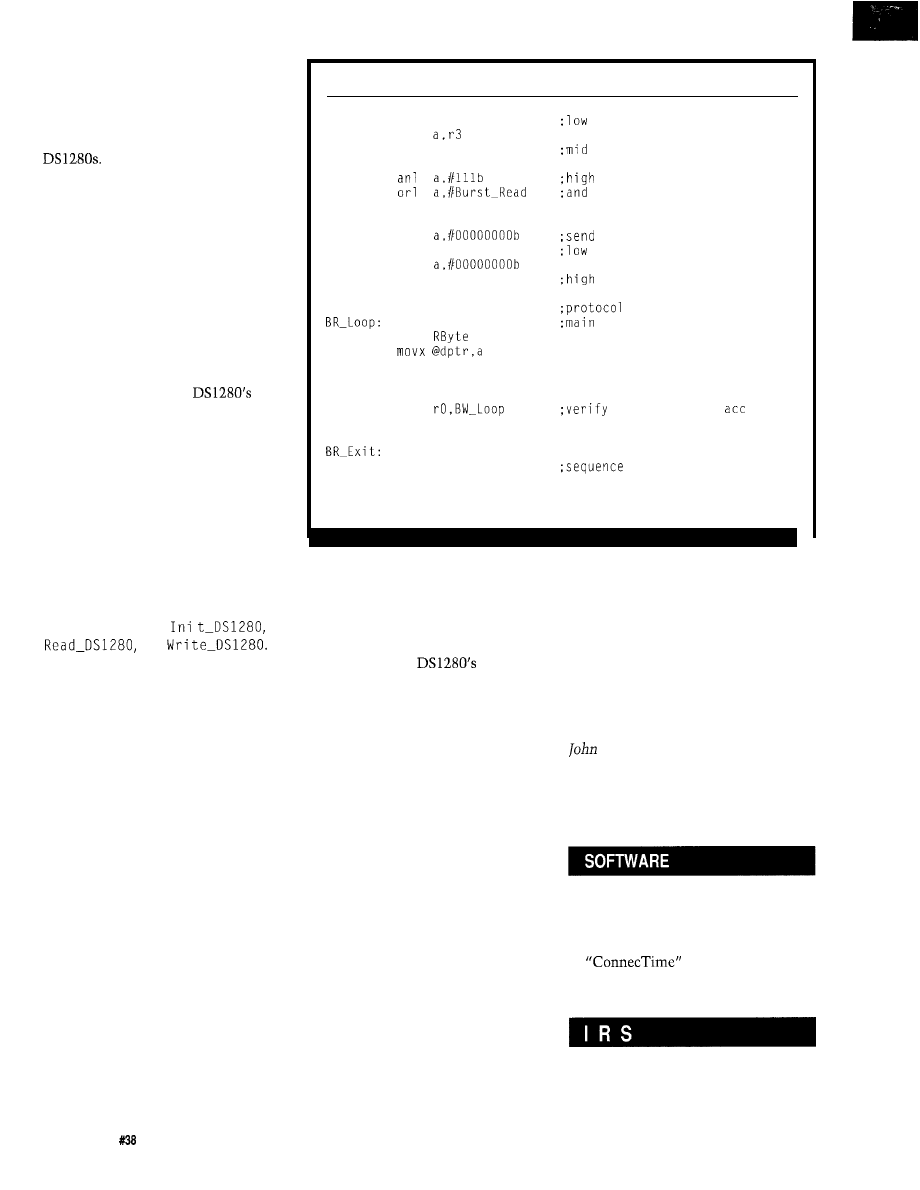
information, the remaining five bits
denote a specific command.
Two bytes of selected bits are
sent. These bits are intended to
identify and differentiate multiple
A CRC byte is computed
over the entire command sequence and
is also sent.
If the CRC is received correctly at
the DS1280, the requested operation is
carried out. If a CRC error is encoun-
tered, any further processing is
terminated.
These steps must be followed for
each access to the DS1280. The
signaling overhead is made more
palatable because you can transfer
sizable chunks of data using bursts
that autoincrement the
internal address generator at the
conclusion of each byte. When using
most general-purpose controllers, the
DS1280 can handle the transfer rate
about as fast as you can clock it. Now I
will present some driver code for the
DS1280 to better describe how it really
works.
TEST DRIVING THE DS1280
Listing 2 shows three user-callable
support routines that are used to
operate the DS1280:
and
It’s best to start with little pieces and
work your way up. The first routines
in this listing are defined to perform
local support functions such as
computing and verifying the CRC, and
transferring bytes into and out of the
DS1280. The remaining routines are
accessible to higher layers and can do
useful things now that the low-level
stuff exists.
The initialization function is
present since anything that operates
with a serial interface usually needs
some setup. What may be surprising is
the amount of work this routine has to
perform. After setting the I/O bits to
their default state, the code drops
through and sets the select bits to a
known state. The select bits must be
known in order to perform any useful
RAM-related functions with the
DS1280 since the DS1280 is not
battery backed. As I mentioned, in any
RAM operations, the transmitted
select bits must match the select bits
Listing
2-continued
call XByte
address bits
mov
call XByte
address bits
mov
a,r3
address bits
burst read command
call XByte
mov
select bits
call XByte
select bits
mov
call XByte
select bits
mov
a,CRC
call XByte
CRC value
read loop
call
inc dptr
call XByte
djnz
CRC, result in
call Check-CRC
clr RST
is complete
ret
end
within the DS1280. It is possible to
read the current select bits without
knowing what they are, so I first read
the select bits so I can write new select
bits. Now I have the necessary infor-
mation to tap the
capabili-
ties.
Burst-read and burst-write rou-
tines follow the same general guide-
lines used in the initialization se-
quence. The inclusion of the read CRC
command guarantees that the DS1280
has received or transmitted the same
data that I thought it did. This suc-
cess/failure information is communi-
cated up to the higher-level processes
where the appropriate actions can be
taken should an error be detected.
SWITCH IN, SWITCH OUT
Developers of small embedded
systems seem to be succumbing to the
memory glut. In some cases, applica-
tions will benefit from this increase in
storage capacity with added features
and capabilities. Then there are those
applications that would simply not be
possible otherwise. In any case, if you
play it right, the end result can be
product differentiation and superiority.
This is, after all, the ultimate goal.
Considerable amounts of memory
can be accommodated by even the
smallest of controllers. Using bank
switching you can lash tons of RAM to
any controller. With serial methods,
even computational midgets can have
the memory capacity of an Einstein.
Next month, little memories.
q
Dybowski is an engineer in-
volved in the design and manufacture
of hardware and software for indus-
trial data collection and communica-
tions equipment.
Software for this article is avail-
able from the Circuit Cellar BBS
and on Software On Disk for this
issue. Please see the end of
in this issue for
downloading and ordering infor-
mation.
419
Very Useful
420 Moderately Useful
421 Not Useful
80
Issue
September 1993
The Computer Applications Journal
within the past three years dealing with spread spectrum,
and that would review them in a later issue. This exciting
new field offers many radically new approaches to commu-
nications and other areas. It is something about which even
a superficial knowledge would benefit engineers in many
fields. While cannot go into all the gory theoretical aspects
of spread spectrum (SS) in this column, I hope to give you a
nodding acquaintance with the subject by discussing a few
of the more interesting applications gleaned from the patent
search. You will see how SS fits well into this month’s
theme of “signal processing,” for that’s precisely what the
entire concept is all about!
Simply stated, the idea behind SS communications is to
spread the normally, somewhat narrow, spectrum of a
signal over a much wider band of frequencies. In this way,
the total power level used for transmission now appears as a
minute amount of power at any one frequency, or over a
narrow band of frequencies. The benefits of doing this are
many-fold. The signal becomes nearly undetectable by a
narrow-band receiver since there is so little energy within
the narrow
of such a receiver. While a wide-band-
width receiver passes the entire signal, it is still undetect-
able unless the specific spreading code is known, because
the spreading was done in a pseudorandom manner.
Either of two techniques are employed for spreading a
signal. One is “frequency hopping” in which the carrier
frequency of the emission is periodically or continuously
altered in a (pseudo] random manner. The other is “direct
sequence” SS in which a fast, pseudorandom, digital noise
(PN for “pseudonoise”) generator is used to modulate the
carrier. The meaningful information is modulated onto the
noise source. When the signal is spread over a wide band of
frequencies, the fading that is due to multipath propagation
is vastly reduced. So, too, is the effect of random noise and
narrow-band interference on the decoded signal. Moreover,
it is even possible for a number of stations (signals) to
occupy the same frequencies at the same time, as one looks
like “noise” to the other. This is true since they use
different, and relatively uncorrelated, spreading codes.
When using binary coding, the RF carrier’s amplitude,
frequency, or phase is simply shifted between two states.
Binary data, however, is not applied directly to the trans-
mitter. Rather, each bit of the underlying signal (the data] is
represented by many (typically hundreds or even thousands)
of bits of the PN code. A zero (of the data) lets the PN code
modulate the transmitter directly, while a one inverts the
PN code. On the receiving end, it is necessary to generate a
copy of the original PN code in order to synchronously
demodulate the bit stream and recover the data. Since many
(thousands of) bits of the PN code represent one data bit,
there is a large integration process that takes place, and this
represents the “processing gain” of the system-a real gain,
just as though one increased the power of the transmitter,
the sensitivity of the receiver, or used a better antenna.
With that as a thumbnail description of SS communica-
tion, let’s look at some applications uncovered in the patent
review. Abstract
1
proposes to use SS to provide a return
link in a cable TV system. As you can see from the abstract,
Patent
Number
Issue
Date
1990 03 27
Inventor(s)
State/Country
Assignee
Pidgeon, Rezin E., Jr.; Zendt, Frederick T.; Thompson, Leo J.
GA
Scientific-Atlanta, Inc.
US References
Title
Cable television spread spectrum data transmission apparatus
Abstract
Apparatus for transmitting data spread across at least a portion of the bandwidth of a cable television channel
comprises a carrier signal oscillator, a frequency divider, a pseudorandom sequence generator, and two exclusive
OR gates. A first exclusive OR gate serves to spread a data signal across the pseudorandom noise sequence
generator having a much higher chip rate than the bit rate of the data signal. The second exclusive OR gate
modulates the spread spectrum data signal to a carrier frequency for transmission over the cable television
channel. The apparatus may be applied for return path transmission in the
band which is highly
susceptible to interference noise and provides approximately a
signal to interference ratio advantage over
known data coding and transmission schemes. A microprocessor normally present in a cable television terminal
may format data for transmission, control the spread spectrum modulation process, and control gain control
circuitry for introducing an appropriate power level into the cable plant.
82
Issue
September 1993
The Computer Applications Journal
Patent Number
Issue Date
1990 03 27
Inventor(s)
State/Country
Assignee
James W.
NJ
AT&T Bell Laboratories
US References
Title
Abstract
Self-synchronous spread spectrum transmitter/receiver
The present invention relates to a self-synchronous spread spectrum transmitter and an associated remote spread
spectrum receiver which communicate with each other by the transmission of both (1) a spread spectrum Pseudo
Noise Code (PNC) sequence signal, and (2) a combined PNC sequence plus the data information (PNC+data)
signal. The two signals can be transmitted concurrently using either different frequency bands or on a quadrature
carrier; or the two signals can be transmitted with a time offset between signals. At the receiver the PNC and the
PNC+data signals are separately recovered for the case of the concurrent transmission techniques, and directly
mixed to despread the received signal and recover the data signal at baseband. For the time offset technique, the
delay provided in one of the time offset signals is again introduced to the previously delayed signal, and the
delayed and undelayed signal portions of the received combined signal are directly mixed and then low pass
filtered to recover the data signal. Such techniques eliminate the necessity for providing PNC acquisition and
tracking circuits in associated spread spectrum transmitter and receiver combinations,
a
rather
conventional, direct-sequence, SS system uses a
the microprocessor normally found in the cable TV box to
binary PN code generator to spread the data signal. Since all
carry out the SS encoding operations.
operations are performed on binary data up to the point of
As you saw in the previous patent, the ability to
modulation onto the carrier, this is accomplished with a
despread a received signal is dependent upon having a local
simple XOR circuit. Note the use of the term “chip” to
copy (at the receiver] of the PN code used at the
refer to the bits of the PN code, reserving “bit” for the data
ter. In addition, this code generator must be perfectly
stream. Here, as always, many chips are used to make up
synchronized to that of the transmitter. Much effort and
each data bit. This results in the “processing gain” when
complexity in SS designs relates to generating this
these chips are synchronously integrated at the receiver to
nized PN code. Abstract 2 for a patent by AT&T Bell
recover the data stream. As pointed out, SS offers its many
Laboratories proposes to solve this problem by eliminating
benefits to this application: immunity to noise normally
the local code generator completely! Instead, they send the
found in the 030-MHz return path band, improved
code itself along with the data. There are a number of
to-noise ratio due to the processing gain, and utilization of
means for accomplishing this feat. Different frequencies/
Patent Number
Issue Date
Inventor(s)
State/Country
Assignee
US References
19901016
Nease, Greg A.; Cripps, Peter K.
NJ
Agilis Corporation
Title
Abstract
Differential correlator for spread spectrum communication system
A spread spectrum communications system includes an encoder for differentially encoding a spread spectrum
spreading code sequence in accordance with an input data signal. Each chip of the spreading code sequence is
inverted, or not inverted, relative to the polarity of a corresponding chip of the spreading code sequence a fixed
time delay previously, depending on whether the input data is a logic one or zero, respectively. At the receiver, the
data is recovered in a differential data decoder wherein the presently received chip of the spread spectrum signal
and a corresponding previously received chip of spread spectrum signal, received a fixed time delay previously,
are compared one chip at a time. Since it is the spreading code sequence that is differentially encoded and differ-
entially decoded, there is no need for a synchronized code sequence generator at the receiver, and data synchro-
nization is achieved after one cycle time of the received spread spectrum spreading code sequence has elapsed.
The Computer Applications Journal
issue
September 1993
bands for signal and PN code may be used, or the two
components may be sent at two different times. Most
likely, though, they would be sent in quadrature on the
same carrier at the same time. Obviously, some of the
secure communication capability of SS is compromised by
doing this. For, if the code is known to all listeners, then
anyone is able to despread the signal and recover the data.
But the reduction in circuit complexity and associated cost,
size, and power would make this unique approach of value
in many applications where security is not the prime focus.
Abstract 3 addresses this same problem of creating a
synchronized PN code source in a different way. Here, the
Agilis Corp. proposes to actually transmit the PN code in a
manner that it may be easily recovered at the receiver. As
the code generating process proceeds, information is
code itself can be extracted at the receiver by simply
performing an XOR function on a received chip with one
that is offset by the same amount as in the encoder. Once
the PN code is known, it can be used in the decoding
process. The decoder simply has to (continually) XOR the
input chip with one that arrived at the fixed offset earlier,
and then invert or not invert the local PN code accordingly.
The result is the original data!
Often, the prime reason for using SS is to make the
signal secure from intercept. The patent described in
Abstract 4 from Sandia Labs uses SS in an underwater
beacon system. In this case, it is absolutely necessary for the
listener to have an exact copy of the PN spreading code. For
without it, the signal appears to be just so much ocean
background noise! Note also how this system benefits from
encoded on this PN code by inverting or not inverting chips
the
advantages of SS. Signals are enhanced by the
in the code relative to chips offset by some fixed time.
“processing gain” which provides increased range and
initially all “0” data bits are sent, for example, then the PN
jamming resistance. Also, by using a different PN code for
Patent
Number
Issue
Date
Inventor(s)
State/Country
Assignee
US References
Title
Abstract
1990
08
21
Shope, Steven M.
N M
Sandia Research Associates, Inc.
Spread spectrum underwater location beacon system
An underwater location beacon emits a continuous wave signal which is phase-shift modulated by a pseudo-noise,
spread spectrum code. This signal is detected with an exact replica of the transmitted code. To an unauthorized
observer without the replica, the transponder’s signal is indistinguishable from background ocean noise. The
spread spectrum code allows extraction of the signal from high levels of ocean noise, providing an increased
detection range, jamming resistance, covertness, and unique signals for each pinger. The outputs of the surface
spread spectrum receiver are used with automated location algorithms. Several receivers at different surface
positions provide the underwater coordinates of the pinger’s location.
Patent Number
Issue Date
Inventor(s)
State/Country
Assignee
US References
1990 12 11
Arthur, James D.; Sanderford, H., Jr.; Rouquette, Robert E.
CA
Axonn Corporation
Title
Abstract
Wireless alarm system
A wireless alarm system using spread spectrum transmitters, fast frequency shift keying, spread spectrum
receivers, and computer with a display. The spread spectrum transmitter includes an oscillator coupled to a
microprocessor with chip code generation means, preamble register, address register, and data register. The
spread spectrum receiver acquires synchronization of the spread spectrum signal using a microprocessor coupled
to the quieting, signal strength, or baseband output of the receiver, with a two-step algorithm. The steps comprise
achieving a coarse lock and a fine lock to the spread spectrum signal.
84
Issue
September 1993
The Computer Applications Journal
each “pinger” (underwater transmitter), all transmitters
may operate in the same frequencies at the same time
without interfering with one another. A few, smart surface
receivers-using a lot of digital signal processing-can each
extract all of the signals within range, and from them
determine the location of all the “pingers.”
Abstract 5 describes a wireless alarm system which
uses SS techniques. The problem of synchronizing PN codes
again appears, and a two-step procedure for achieving coarse
and fine synchronization using a microprocessor is men-
tioned. The numerous references should be useful for
anyone interested in using SS in such an application.
Lastly, I found the patent discussed in Abstract 6 to be
only begun to mention the voluminous theoretical and
design considerations involved. But I hope this has provided
an introduction to those of you who have no familiarity
with this rapidly evolving field, and might serve as a source
of reference material for further exploration.
Russ Reiss holds a Ph.D. in
and has been active in
electronics for over years as industry consultant,
designer, college professor, entrepreneur, and company
president. Using microprocessors since their inception, he
has incorporated them into scores of custom devices and
products. He may be reached on the Circuit Cellar
BBS or on CompuServe as
a somewhat amusing and certainly novel (yet useful)
application of SS. No longer when playing golf must you
only estimate your distance from the pin. By using a
number of low-power SS transmitters located at each pin,
and a hand-held decoding receiver, the golfer can get an
instant readout of his distance. This application, once again,
makes use of the many benefits of SS that we’ve seen above:
the ability to use low-power transmitters, the sharing of
frequencies by many transmitters, and the ability to do
ranging based on precisely timed signals from multiple
sources. In essence, this is a mini-GPS system brought
Patent abstracts appearing in this column are from the
Automated Patent Searching
database from:
25 Science Park
New Haven, CT 065 11
(203)
or (800) 648-6787
.
down to Earth!
Obviously, we’ve only touched on a few of the many
application areas for spread spectrum technologies. And I’ve
422
Very Useful
423 Moderately Useful
424
Not Useful
Patent Number
issue Date
Image Disc
Inventor(s)
State/Country
US References
US Class
Class
Title
Abstract
1991 1008
This patent is on Patentlmages
Wang, James J.;
Robert M.
CA
3421450 3421451 3421458 3421463
3641561 3641460
GO1 S
2
Golf course ranging and direction-finding system using spread-spectrum radio location techniques
The invention disclosed herein is directed to a method and apparatus which employs a spread-spectrum based
radio location system, using handheld receiver units and fixed-position reference transmitters, to determine
distance and direction between a golfer and key locations on a golf course, such as the distance and direction to a
particular pin. The plurality of timing reference transmitters which are located throughout the vicinity of the golf
course broadcast a spread-spectrum ranging signal consisting of a radio-frequency carrier directly modulated by a
periodic pseudonoise (PN) coded or similar sequence. Each transmitter broadcasts at the same RF signal but a
unique PN-coded sequence is assigned to each transmitter. Golfers are provided with the handheld receiving unit
which receives the transmitter spread-spectrum signals and which synchronizes to the spread-spectrum signals in
order to obtain range estimates to a selected set of reference transmitters. The handheld receivers also include
memory to store the coordinates of the reference transmitters and the pin positions and other reference points for
each hole on the golf course, which are either preloaded into memory or transmitted (as modulating data) with the
ranging signal. Each handheld unit also includes a digital processor which incorporates a hyperbolic location
algorithm to compute the handheld unit position based on the estimated ranges to the selected transmitters and
the reference transmitter coordinates. The distance and direction from the current position to the pin or other
selected reference points is then displayed via an appropriate medium on the handheld unit.
The Computer Applications Journal
September 1993
85

The Circuit Cellar BBS
bps
24
days a week
(203) 871-l 988-Four incoming lines
Vernon, Connecticut
This month, we’re going to ignore computers (to some extent) and
concentrate on radio and chemistry. In the first thread, we get a
lesson in radiated RF, not the kind
radiates from a computer, but
kind that can interfere with a computer.
Next, we follow up on robotics threads from a few months
ago and look at what if fakes to make an inexpensive radio modem
to connect a robot with a base station.
Finally, as a follow up to the engine monitoring thread from last
month, we discuss the actual engine chemistry and how if affects
performance and emissions.
RFI affecting the computer
From:
To: ALL USERS
Has anyone had any experience with interference from
HF radios affecting computers? The radio in question is 300
watts PEP operating on frequencies from
1.8 to
25 MHz. I
know there can be interference in some cases. Has anyone
ever heard of it causing permanent damage to a hard drive
or a monitor? I would be especially interested in hard data,
field strengths, and so forth.
From: MICHAEL MILLARD To: ROBBIE LAIRD
The type of radiation you are referring to here is known
as nonionizing radiation, and, yes, it has been known to
cause the sorts of trouble you are experiencing. It is difficult
to offer advice on the matter because every case is different.
In your case, I gather the offending transmission is a
sideband transmission, in which case your calculated
wattage may not actually reflect the peak-isotropic radiated
power. But let’s assume it’s under a kilowatt in any event.
One of the first things we need to know is the proxim-
ity of the radiation source(s) to the devices being interfered
with. If the two are located VERY close to each other (and
presumably, you) you may also want to consider if the HF
transmission represents a hazard to personnel and that the
station does in fact comply with OST Bulletin
regarding
human exposure limits to nonionizing radiation. (I have a
spreadsheet that will make this determination easier if you
know enough about the HF antenna system.) In which case,
moving the HF “source” farther away to solve one problem
may end of solving them both. (You can get OST-65 from
the FCC’s Office of Science Technology or any govern-
ment bookstore.)
But let’s assume that the antenna is NOT “underfoot”
and that you are under the guidelines of OST-65 with a field
density of not more than
1
in the general vicinity
of the malfunctioning equipment..
Normally, that power level would not cause objection-
able or permanent impairment to most types of equipment.
Shielding may help equipment that was poorly designed to
work in moderate RF fields. (Another way of saying this is
that crappy equipment works like crap. You may find that
some other manufacturer’s gear of the same type will work
when others won’t.) Part
15
of the FCC rules will give you a
little more indication of what should be expected to work,
and what should not be in the presence of the RF levels we
are assuming here.
Now, the real meat and potatoes. Perhaps the root
cause is “conducted” noise and is not in fact a direct
radiation problem at all. You can check this by eliminating
as many “outside paths” as practical to see if the interfer-
ence subsides in any way. Running from a UPS, disconnect-
ing and terminating any used or unused inputs and outputs,
and trapping RF at the ports are all good checks. You may
also have a strong localized field in the vicinity in which
your equipment is located. This may be caused by ground
reflections of the HF transmission
(1.64
x the radiated field,
typical) or by more local reflections caused by the building’s
construction or somesuch. Not too much you can do about
this unless you have access to the HF antenna design/
orientation. Remember that low frequencies such as these
typically do not have high-gain antennas, and thus the
vertical field component of the RF signal is very broad. The
long wavelengths involved make higher-gain systems
impractically large. So look for vertical fields (straight down
the tower with no reflection to be around 60% or more).
This number may be even higher if the HF antenna design
radiates in both the vertical and horizontal planes (which I
doubt it does.)
One last note, you might check with the HF operator to
see if the antenna(s) system(s) is/are “loading-up” properly.
A high VSWR can cause harmful reflections (not only to
you, but to the RF gear). Correct the match to see if that
helps. If the antenna doesn’t load too well, a worthwhile
86
Issue
September 1993
The Computer Applications Journal
check might be to adjust the match to see if your problem
gets any better or worse. Obviously, the HF transmitter
itself ought to be in good working order.
But above all, KEEP IN MIND, that you may be dealing
with a “coupling” problem which may change from day to
day. Perhaps a dry atmosphere will offer less attenuation on
one day than the morning after a strong storm.(?) It’s
important to look at real improvements over time to
evaluate the effectiveness of any presumed “fix.”
Inexpensive radio modems
From: DERRY BRYSON To: ALL USERS
A friend an I are building small (not tiny] mobile robots
and are trying to work out a CHEAP radio modem setup.
Our robots pack PC motherboards, floppies, and so forth, so
we decided to try to use standard internal modems and
cordless phones.
We were able to connect two modems (and computers)
together using a 9-V battery spliced into a small piece of
phone line [to sort of simulate a phone line). We then took
this a step further and built another of these simulated
phone lines and connected a phone to each modem and
then laid the handsets next to each other with ends re-
versed. We were easily able to connect at 2400 bps (as long
as no one whistled).
Anyway, the next step was to connect a modem to the
base of a cordless phone. Now the problem: how do we wire
the cordless phone handset into our simulated phone line
for the other end?
We have tried using a transformer scavenged from a
dead modem with one side hooked to our simulated phone
line and the other hooked to the mic, speaker, and ground
from the handset (i.e., the mic and speaker leads are
connected together through pots to one lead on the trans-
former, ground is connected to the other lead on the
transformer). Doesn’t seem to work.
We have considered using a cheap phone and connect-
ing the mic and speaker leads from the cordless phone
handset to the speaker and mic leads on the cheap phone,
respectively. Either directly or maybe through isolation
transformers (Radio Shack S-ohm to
Then, of
course, connect the cheap phone to the modem on the
robot.
From: PAUL PETERSEN To: DERRY BRYSON
Why not just use a cheap walkie-talkie from Radio
Shack? They have a 46-MHz version for $10 or so. It’s a
kiddie model, but it does two-way communication with a
low-power transmitter and receiver. There’s even a button
for sending Morse code beeps. Are you circuit design
proficient? Have you tried light beams instead of radio
waves? Sounds like a fun project..
From: DERRY BRYSON To: PAUL PETERSEN
I bought two walkie-talkies from Radio Shack (49
and have even built some boards that connect to a serial
port with tone generators and decoders (567s) which almost
work. These have three problems: the communication is
only half duplex, the 567s are slow and I don’t think I will
be able to achieve anything beyond 300 bps, and there is
interference on the band that they use in my area.
Communication using light has the problem that it
won’t travel through walls, which means putting transmit-
ters in each room and running a lot of wire.
If we could just figure out how to couple the cordless
handset to a phone line we would be set.
From: J. DEBERT To: DERRY BRYSON
started a similar project some time ago (although I
never finished it], so I may have a useful suggestion.
I chose the
as the modem chip to get
1200 bps (Bell 202) and ran it through a buffer to a Radio
Shack
I realized there would be problems
from interference caused by other radios, so I chose the
channel hand-held. The hardware is connected to a
microcontroller which controls all of the modem chip
functions and transmit/receive and channel selection. I
haven’t worked out the details of how to establish a link
and all, but I’m certain that it’s possible-unless all the
channels are occupied. In most areas, it’s unlikely that all
the channels would be in use close enough to you to cause
bad interference. Since this design allowed only for simplex
communications, owing to the use of only one channel,
I
thought of using some kind of “packet” style of communi-
cation, where the sender sends a packet, stops transmitting,
then the receiver transmits a response, and so forth.
From: DERRY BRYSON To: J. DEBERT
These chips sound interesting, are they readily avail-
able? I might want to try them with the walkie-talkies I
have when I build my next robot. I am planning on making
it much smaller and basing it on an 805 which has serial
ports, but would need the modem part.
As I mentioned in my previous message, I have built
some circuits using 567s as tone decoders (and generators,
as well), but the 567 is too slow (needs something like 10
The Computer Applications Journal
issue September 1993
8 7
wave fronts, which means maybe 300 bps using a
tone]. The modem chips sound like something to try, but I
wonder about the bandwidth or distortion on the
talkies. Can they faithfully transmit and receive the signals
from these chips?
From: J. DEBERT To: DERRY BRYSON
The bandwidth of the radios should be more than
sufficient. The modem chip-the
a voice-band
modem designed for telephone use. It is used also in
amateur packet radio systems. I don’t recall off-hand what
all the modes are, but I remember that Bell 103, Bell 202,
CCITT V.21 are available. It can be connected directly to
your micro’s bus with address decode circuitry.
From: MICHAEL MILLARD To: PAUL PETERSEN
A simple observation..
performance
0.0001 _ f(c)
1
aggrevation f(p)
where
f(c) = chances of the damn thing working at all much
less on the first try
f(p) = the number of people likely to notice
From: MICHAEL MILLARD To: DERRY BRYSON
If you’re looking for something off-the-shelf, here’s an
interesting ad I ran across last week..
Not something I normally do, but let me quote verba-
tim out of an ad in last month’s issue of Wireless Design
and Development,
page 52:
“The
Wireless Digital Modem model, the
makes it possible to create networks consisting of
point-to-multipoint links over urban, suburban and rural
areas, without a license. The 64MP products operate in one
of the FCC-designated Part 15 (902-928 MHz) frequencies.
They can be used quickly and painlessly to replace or
extend multidrop
modems or licensed multiple
address radio systems. The device offers synchronous and
asynchronous operation at data rates up to 64 kbps. Cylink,
3 10 North Mary Ave., Sunnyvale, CA 94086”
Another option might be to look into an outfit called
Electronics
They make an FM
(450-470 MHz) unit which comes with software for up to
48 nodes. Also supports X.30 for DEC and IBM hosts and
Costs start around $500 for the two-board set. But
that’s serious hardware.
If you are sending simple commands (and I gather you
are not or else you wouldn’t want high data speeds), DTMF
is always a simpler solution, at least when it comes to
transmitter interfacing.
From: DERRY BRYSON To: MICHAEL MILLARD
Both of these sound too expensive. This is just a hobby
robot after all.
Basically, I will be sending simple commands. Some-
thing like Right 90, Forward 100, Right 45, and so forth
(actually, probably more like
and requesting
simple information from the robot like a distance read from
a sonar ping or maybe a whole 360” scan. It is too bad that
DTMF has only 12 combinations, if there were 16 we could
send a nybble at a time.
We have actually got it pretty much working now. I can
only achieve 1200 bps error free with my cordless phone
(my friend’s phone will do 2400 bps), but I think that will
be fast enough for now. We are now able to remotely pilot
the robots using CTTY and running the programs we used
before that required typing commands from the keyboard.
Pretty exciting.
From: MATTHEW TAYLOR To: DERRY BRYSON
Sounds like you’re having success currently, so this
probably won’t help, but DTMF DOES have 16 combina-
tions. It is really a four-by-four matrix and I’d bet that most
encoders/decoders support all 16 since all the HW is already
there to do it!
Gasoline engine chemistry
From: GARY OLMSTEAD To: ALL USERS
On the topic of gas engines, what is the difference
between “air-fuel ratio” and “lambda”? I have formulas for
both and they are very similar. The formulas calculate the
desired result by measuring the ratios of the various
exhaust gases. The formula for air-fuel ratio is not reliable
for oxygenated fuels; does this hold for lambda?
From: THOMAS BARNETT To: GARY OLMSTEAD
Lambda means the “excess-air ratio” and is given as
lambda = quantity of air supplied/theoretical requirement =
A lean mixture (lambda 1) contains more air while a
rich mixture (lambda 1) contains less air. Spark-ignition
engines attain maximum power with an air deficiency of
10% (lambda = l-0.9) and minimum fuel consumption with
roughly 10% excess air (lambda 1.1).
Issue
September 1993
The Computer Applications Journal
From: GARY OLMSTEAD To: THOMAS BARNETT
Thank you for the response. Just one more thing:
fuel ratio falls apart for oxygenated fuels; does this also hold
true for lambda?
From: THOMAS
To: GARY OLMSTEAD
try to explain the lambda ratio as best as I under-
stand it as it applies to oxygenated fuels. First, the value of
lambda between a rich mixture and a lean mixture will
change only between 0.975 for a rich mixture and 1.025 for
a lean mixture. This may vary plus or minus a few hun-
dredths. That value is determined by the lambda sensor
housed just ahead of the catalytic converter in the system
exhaust. Part of the lambda sensor is housed within the
exhaust system, the other part is exposed to ambient air.
As the sensor heats up to a temperature of approxi-
mately
it begins to conduct oxygen ions. There is a
certain amount of residual oxygen expelled after combus-
tion. If there is a difference between the electrodes of the
sensor [i.e., the one exposed to the exhaust and the one
exposed to ambient air), a voltage jump will occur indicat-
ing whether the mixture is richer or leaner than lambda =
1.
[That, by the way, is called stoichiometric mixture if you’re
interested in big words.) This window of change is very
small, occurring between 1 and 0.001.
That information is used by the vehicle computer to
determine whether more or less air is required for combus-
tion. Normal air-fuel mixture is determined by the throttle
setting, so the lambda ratio will either add to or take away
from the throttle setting. Enter oxygenated fuels.
The reason for adding oxygenates is to reduce carbon
monoxide (CO) and hydrocarbons (HC). With oxygenated
fuel, the engine excess air factor is lambda 0.9, so this will
remain fairly constant because the oxygenates will keep the
large excess air factor or change from occurring. Since
engine operation is already in the rich range (lambda
you will get lousy acceleration and poor fuel consumption,
which you’ve probably noticed. On the other hand, you’ve
gobbled up most of the CO and HC. That’s my best shot.
From: BRAD DAVIS To: THOMAS BARNETT
I know the message wasn’t to me, but I was “lurking”
and would like to thank you for the message. I experience
about a 20-25 % decrease in fuel economy when using the
oxygenated fuels in the winter. I live in Colorado Springs
(about
feet) and the air is already thin enough that
my acceleration is much less than what it is when near sea
level. Anyway, here’s the question: do the oxygenated fuels
decrease CO and HC emissions by more than 20-25 % I
would hope that since I need to burn an additional
of gas to go somewhere (at a reduced acceleration), the HC
and CO emissions would drop by more that a few percent.
From: THOMAS BARNETT To: BRAD DAVIS
This is a tough question to answer because a number of
things are happening. It also depends on how old the vehicle
is and what type of catalytic converter is installed. Basically
for most newer vehicles there is almost complete CO and
elimination by catalytic afterburning. Complete
combustion would produce only carbon dioxide and water,
both harmless byproducts, if you in fact had complete
combustion. is easy to see that that simply does not
happen-just look at the sky.
There are many incomplete combustion
paraffins, olefins, aromatic hydrocarbons, aldehydes,
ketones, carboxylic acids, acetylene, ethylene, hydrogen,
soot, polycyclic hydrocarbons, oxides of nitrogen-and if
you use leaded gasoline the added burden of lead oxides and
lead halogenides along with fuel impurities such as sulfur
oxides. Then insert a little sunlight and come up with
organic peroxides, ozone, and peroxyacxetyl-nitrates.
YOU
probably need to be a chemist to know what all that means.
Here in Las Vegas, it means brownish-green haze that
hangs over the city and only leaves when the wind blows at
40 MPH or more. So to answer your question, probably not.
Pray for a high wind!
We invite you call the Circuit Cellar BBS and exchange
messages
and files
with
other
Circuit Cellar
readers. It is
available 24 hours a day and may be reached at (203)
1988. Set your modem for 8 data bits, 1 stop bit, no parity,
and 300,
9600, or
bps.
Software for the articles in this and past issues of
The
Computer Applications
may
be downloaded from
the Circuit Cellar BBS free of charge. For those unable to
download files, the software is also available on one 360K
IBM PC-format disk for only $12.
To order Software on Disk, send check or money order
to: The Computer Applications Journal, Software On Disk,
P.O. Box 772, Vernon, CT 06066, or use your VISA or
Mastercard and call (203) 8752199. Be sure to specify the
issue number of each disk you order. Please add $3 for
shipping outside the U.S.
425 Very Useful
426 Moderately Useful
427 Not Useful
The Computer Applications Journal
Issue
September 1993
8 9

The Collegiate Challenge
can hardly believe it but September has rolled around already. Another summer has passed and fall is
about to burst onto the scene. September always reminds me of back to school. Could it be all of those ads I
see that make me think that way? Maybe.
To all of you who are going to back to school, hope your professors took advantage of the special deal we offered to colleges
and universities. If so, I hope you enjoy reading the
Applications
Journal along with all of the materials you will be expected
to read this semester. I also hope you have a successful semester.
Speaking of successful semesters, I can’t emphasize enough how important it is that you apply yourself. Let me tell you a tale of
two students. One student stayed out late every night playing around, doing just enough to get by with slightly better than average
grades, Content with his lot, this student couldn’t wait for all of this agonizing homework to end so he would never have to think about
those complicated subjects ever again. Another student faces the same material as a personal challenge, trying to learn all he can;
trying to absorb as much as he can; trying to rise to the best of his abilities.
Well, finally the day comes that it is over. Graduation. I won’t give you the song and dance about which one of these two
impressed the job interviewers and received the better offer. That would be trite. Instead, ask you to consider which of these
students has formed better self-development skills, Which of these two do we want the country and economy to depend on?
I won’t tell you which of these students I was. Let’s just say I saw the light very early and decided a career as a bum was
defeating. Instead, I ask you to examine yourself to see which kind of student you are. Take this to heart, because after you are out of
the collegiate program, the rest of your intellectual development is up to you. Perhaps you will get “lucky(?)” and land a job in an
organization where all of your efforts are strictly guided by the needs of the company. Perhaps you’ll get “lucky(?)” and land a job in an
organization where you are in charge of whatever you do. Of course, the responsibilities in the latter job mean you get the “bullet” as
well as the praise.
I always prefer the second career path because that’s just the kind of person I am. Personally, I couldn’t begin to think of myself
in any kind of position where I couldn’t apply unrestricted drive and motivation.
So, try to see beyond the immediate tasks of homework or dull career assignments. Look for a deeper lesson in this challenge
you have accepted for yourself. Is your challenge, “How little can I do and still manage to sneak past?” or is your challenge, “How good
at this can I become?” Be true to yourself and honestly appraise your approach.
Those of us who don’t have to go through the grueling rigors of classwork (thank the stars) sympathize with you, but the end
result puts you in a minority among men (and women). How long you stay there just depends on how you apply it.
96
Issue September 1993
The Computer Applications Journal
Wyszukiwarka
Podobne podstrony:
circuit cellar1996 09
circuit cellar2004 09
circuit cellar1995 09
circuit cellar1997 09
circuit cellar2000 09
circuit cellar2001 09
circuit cellar2002 09
circuit cellar2003 09
circuit cellar1994 09
circuit cellar1996 09
circuit cellar2003 09
circuit cellar1994 09
circuit cellar1997 09
circuit cellar1993 09
circuit cellar2004 09
circuit cellar1995 09
circuit cellar1996 09
więcej podobnych podstron