1 (154)
Strona 15 z 46
Spy Circuits
To get good audio ampiification, and a stable oscillator and the ability to handle the Circuit without it driftin transistors. These circuits a re on the fol i owi ng page.
THE TANK CIRCUIT AND "Q"
Before we go to 3-Transistor circuits, there is one factor that needs mentioning. It is the most important part of TANK CIRCUIT
This is the coil and capacitor in the collector of the oscillator transistor.
Even though these two components are classified as "passive" - and do not amplify, when they are connectec form a Circuit known as a TANK CIRCUIT and actually produce a waveform that is larger than the supplied vo components set the frequency of the Circuit and when they are operating correctly, the output will be a maxirm A lot of experimentation has gone into the size of the inductor and by making it 3-4 times longer than the diam thickest wire possible and spreading the turns, the inductance will provide the maximum amount of energy to | capacitor. Not only does the va!ue of inductance and capacitance have to be correct to achieve the desired fre energy from the inductor must match the energy from the capacitor, to get the maximum output.
Ali this is done to achieve a high output and when a tank Circuit is lightly loaded it will oscillate at one and only When this happens and when we measure the output and compare it to the supply voltage we get a value cali Value" or "Q" value.
This value is not known for these circuits but the result of a good tank Circuit can be seen by testing the Circuit Strength Meter or simply detecting the output of the bug at a distance.
Page 2 continues with 3-TRANSISTOR CIRCUITS:
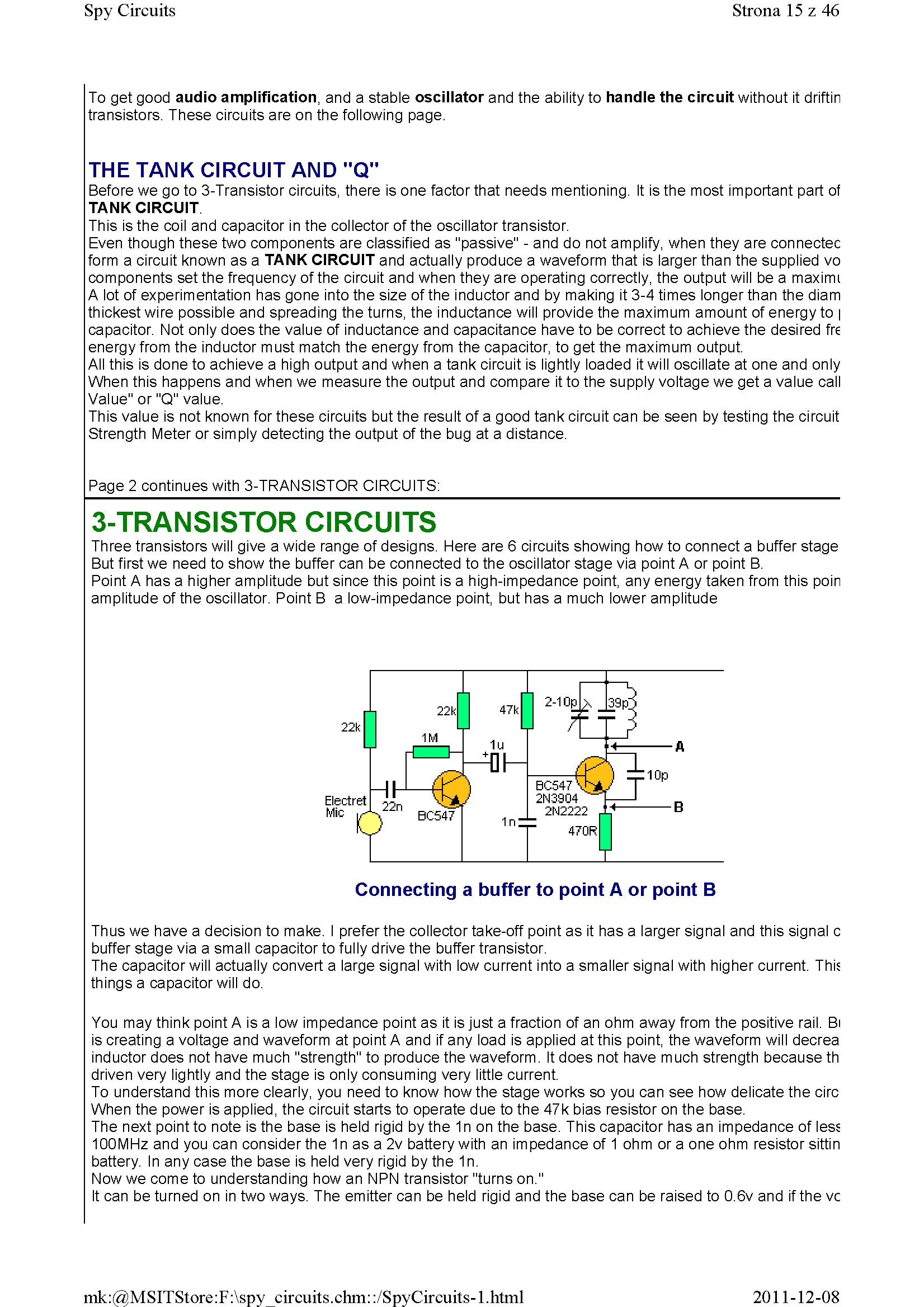
3-TRANSISTOR CIRCUITS
Three transistors will give a wide rangę of designs. Here are 6 circuits showing how to connect a buffer stage But first we need to show the buffer can be connected to the oscillator stage via point A or point B.
Point A has a higher amplitudę but sińce this point is a high-impedance point, any energy taken from this poin amplitudę of the oscillator. Point B a low-impedance point, but has a much lower amplitudę

Connecting a buffer to point A or point B
Thus we have a decision to make. I prefer the collector take-off point as it has a larger signal and this signal c buffer stage via a smali capacitor to fully drive the buffer transistor.
The capacitor will actually convert a large signal with Iow current into a smaller signal with higher current. This things a capacitor will do.
You may think point A is a Iow impedance point as it is just a fraction of an ohm away from the positive raił. Bi is creating a voltage and waveform at point A and if any load is applied at this point, the waveform will decrea inductor does not have much "strength" to produce the waveform. It does not have much strength because th driven very lightly and the stage is only consuming very Iittle current.
To understand this morę clearly, you need to know how the stage works so you can see how delicate the circ When the power is applied, the Circuit starts to operate due to the 47k bias resistor on the base.
The next point to notę is the base is held rigid by the 1 n on the base. This capacitor has an impedance of less 100MHz and you can consider the 1n as a 2v battery with an impedance of 1 ohm or a one ohm resistor sittin battery. In any case the base is held very rigid by the 1n.
Now we come to understanding how an NPN transistor "turns on."
It can be tumed on in two ways. The emitter can be held rigid and the base can be raised to 0.6v and if the vc
2011-12-08
mk:@MSITStore:F:\spy circuits.chm::/SpyCircuits-l.html
Wyszukiwarka
Podobne podstrony:
1 (181) Strona 42 z 46 Spy Circuits coil. Ali the othertransmitters have sufficient output to detect
1 (149) Strona 10 z 46 Spy Circuits2 TRANSISTOR CIRCUITS The next progressive step is to add a trans
1 (162) Strona 23 z 46 Spy Circuits When you fix these faults you will see how much improvement you
1 (167) Strona 28 z 46 Spy Circuits But it is often quite inconvenient to use a long antenna, so her
1 (168) Strona 29 z 46 Spy Circuits A Circuit diagram does not show the screening necessary to keep
1 (176) Strona 37 z 46 Spy Circuits junction of the DC amplifier transistor only allowing ,6v to app
1 (178) Strona 39 z 46 Spy Circuits We needrYt say any morę about construction as you will obvious!y
1 (179) Strona 40 z 46 Spy CircuitsEXPERIMENTING Take the Voyager project and connect 30cm of tinned
1 (182) Strona 43 z 46 Spy Circuits lt s a bit like hundreds of people trying to push a person on a
1 (150) Strona 11 z 46 Spy Circuits magnetic field" and this occurs when the coil collapses and
1 (151) Strona 12 z 46 Spy Circuits - 5v for maximum output. The Voyager has been copied by many kit
1 (157) Strona 18 z 46 Spy Circuits4. DIFFERENT COUPLING We have already mentioned the fact that a c
1 (159) Strona 20 z 46 Spy Circuits8. CLASS "C" OUTPUT The following Circuit uses no biasi
1 (160) Strona 21 z 46 Spy Circuits with frequencies around 100MHz. It seems the designer had diffic
1 (161) Strona 22 z 46 Spy Circuits There is no evidence of the above Circuit de!ivering morę output
1 (163) Strona 24 z 46 Spy Circuits This covers all the possible combinations for the greatest outpu
1 (166) Strona 27 z 46 Spy Circuits corwert a high-voltage at low-current into a low-voltage at high
1 (169) Strona 30 z 46 Spy Circuits You can learn a lot about designing a Circuit by looking at faul
1 (170) Strona 31 z 46 Spy Circuits This means a certain amount of the energy delivered by the 4p7 w
więcej podobnych podstron