®
L200
ADJUSTABLE VOLTAGE AND CURRENT REGULATOR
ADJUSTABLE OUTPUT CURRENT UP TO 2 A
(GUARANTEED UP TO T
j
= 150
°
C)
ADJUSTABLE OUTPUT VOLTAGE DOWN TO
2.85 V
INPUT OVERVOLTAGE PROTECTION (UP TO
60 V, 10 ms)
SHORT CIRCUIT PROTECTION
OUTPUT TRANSISTOR S.O.A. PROTECTION
THERMAL OVERLOAD PROTECTION
LOW BIAS CURRENT ON REGULATION PIN
LOW STANDBY CURRENT DRAIN
DESCRIPTION
The L200 is a monolithic integrated circuit for volt-
age and current programmable regulation. It is
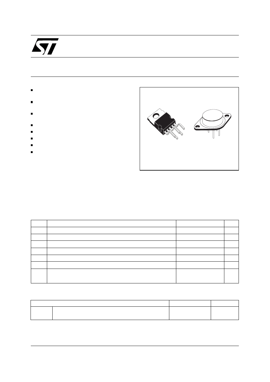
available in Pentawatt
®
package or 4-lead TO-3
metal case. Current limiting, power limiting, thermal
shutdown and input overvoltage protection (up to
January 2000
Pentawatt
®
TO-3 (4 lead)
60 V) make the L200 virtually blow-out proof.
The L200 can be used to replace fixed voltage
regulators when high output voltage precision is
required and eliminates the need to stock a range
of fixed voltage regulators.
Symbol
Parameter
Value
Unit
V
i
DC Input Voltage
40
V
V
i
Peak Input Voltage (10 ms)
60
V
∆
V
i-o
Dropout Voltage
32
V
I
o
Output Current
internally limited
P
tot
Power Dissipation
internally limited
T
stg
Storage Temperature
-55 to 150
°
C
T
op
Operating Junction Temperature for L200C
-25 to 150
°
C
for L200
-55 to 150
°
C
ABSOLUTE MAXIMUM RATINGS
TO-3
Pentawatt
®
R
th j-case
Thermal Resistance Junction-case
Max
4
°
C/W
3
°
C/W
R
th j-amb
Thermal Resistance Junction-ambient
Max
35
°
C/W
50
°
C/W
THERMAL DATA
1/12
2/12
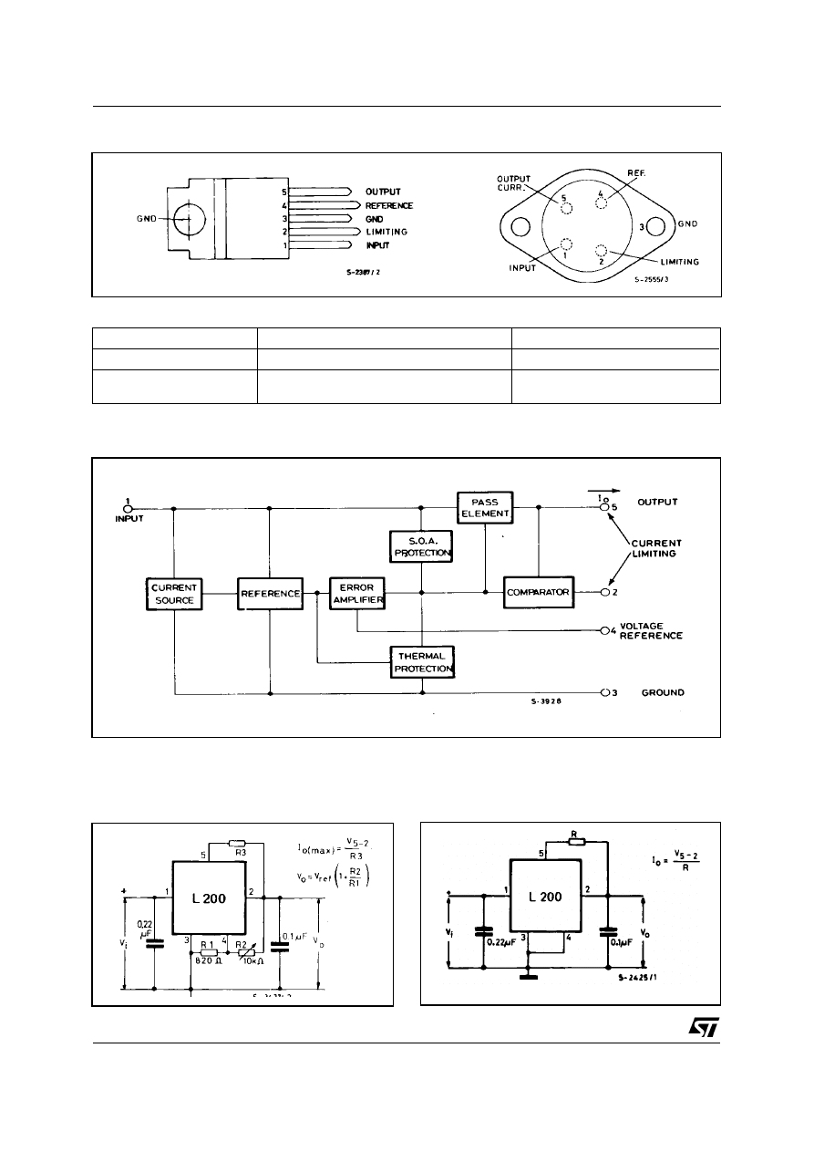
CONNECTION DIAGRAMS AND ORDER CODES (top views)
BLOCK DIAGRAM
APPLICATION CIRCUITS
Figure 1. Programmable Voltage Regulator
with Current Limiting
Figure 2. Programmable Current Regulator.
Type
Pentawatt
®
TO-3
L200
L200 T
L200 C
L200 CH
L200 CV
L200 CT
L200
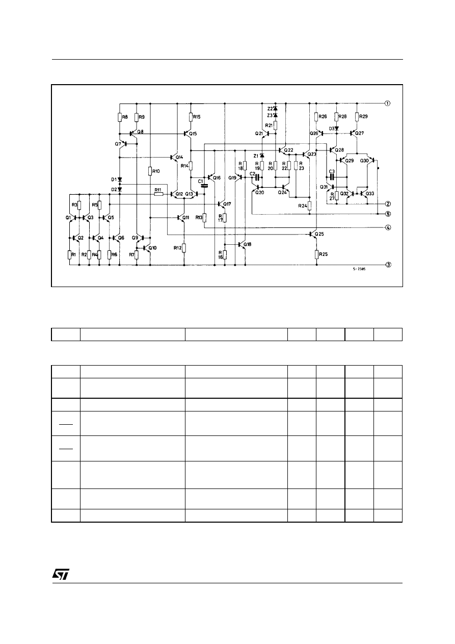
SCHEMATIC DIAGRAM
Symbol
Parameter
Test Conditions
Min.
Typ.
Max.
Unit
VOLTAGE REGULATION LOOP
I
d
Quiescent drain Current (pin 3)
V
i
= 20 V
4.2
9.2
mA
e
N
Output Noise Voltage
Vo = Vref I
o
= 10 mA
B = 1 MHz
80
µ
V
V
o
Output Voltage Range
I
o
= 10 mA
2.85
36
V
∆
V
o
V
o
Voltage Load Regulation
(note 1)
∆
I
o
= 2 A
∆
I
o
= 1.5 A
0.15
0.1
1
0.9
%
%
∆
V
i
∆
V
o
Line Regulation
V
0
= 5 V
V
i
= 8 to 18 V
48
60
dB
SVR
Supply Voltage Rejection
V
0
= 5 V I
o
= 500 mA
∆
V
i
= 10 V
pp
f = 100 Hz (note 2)
48
60
dB
∆
V
i-o
Droupout Voltage between Pins 1
and 5
I
o
= 1.5 A
∆
V
0
≤
2%
2
2.5
V
V
ref
Reference Voltage (pin 4)
V
i
= 20 V I
o
= 10 mA
2.64
2.77
2.86
V
ELECTRICAL CHARACTERISTICS (T
amb
= 25
°
C, unless otherwise specified)
3/12
L200
Symbol
Parameter
Test Conditions
Min.
Typ.
Max.
Unit
∆
V
ref
Average Temperature Coefficient
of Reference Voltage
V
i
= 20 V Io = 10mA
for
Tj
=
-
25
to
125
°
C
for
Tj
=
125
to
150
°
C
-0.25
-1.5
mV/
°
C
mV/
°
C
I
4
Bias Current and Pin 4
3
10
µ
A
∆
I
4
∆
T
•
I
4
Average Temperature
Coefficient (pin 4)
-0.5
%/°
C
Z
o
Output Impedance
V
i
= 10 V V
o
= V
ref
I
o
= 0.5 A f = 100 Hz
1.5
m
Ω
CURRENT REGULATION LOOP
V
SC
Current Limit Sense Voltage
between Pins 5 and 2
V
i
= 10 V V
o
= V
ref
I
5
= 100 mA
0.38
0.45
0.52
V
∆
V
SC
∆
T
•
V
SC
Average Temperature
Coefficient of V
SC
0.03
%/°
C
∆
I
o
I
o
Current Load Regulation
Vi = 10 V
∆
Vo = 3V
I
o
= 0.5 A
I
o
= 1A
I
o
= 1.5 A
1.4
1
0.9
%
%
%
I
SC
Peak Short Circuit Current
V
i
- V
0
= 14 V
(pins 2 and 5 short circuited)
3.6
A
ELECTRICAL CHARACTERISTICS (continued)
4/12
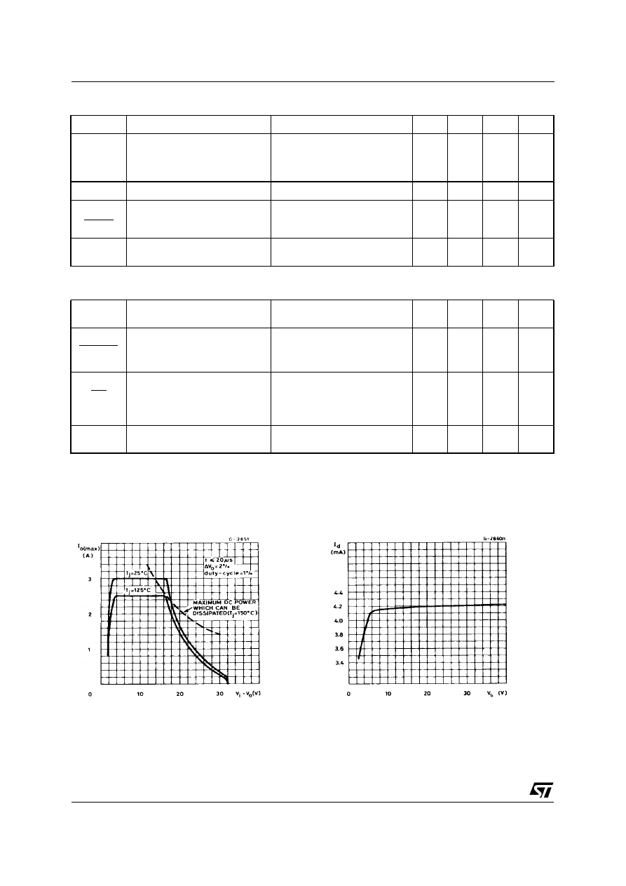
Figure 3. Typical Safe Operating Area
Protection.
Figure 4. Quiescent Current vs. Supply
Voltage.
Note 1: A load step of 2 A can be applied provited that input-output differential voltage is lower than 20 V (see Figure 3).
Note 2: The same performance can be maintained at higher output levels if a bypassing capacitor is provited between pins 2 and 4.
L200
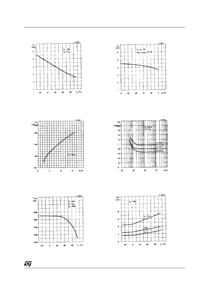
Figure 5. Quiescent Current vs. Junction
Voltage.
Figure 6. Quiescent Current vs. Output
Current.
Figure 7. Output Noise Voltage vs. Output
Voltage.
Figure 8. Output Noise Voltage vs.
Frequency.
Figure 9. Reference Voltage vs. Junction
Temperature.
Figure 10. Voltage Load Regulation vs.
Junction Temperature.
5/12
L200
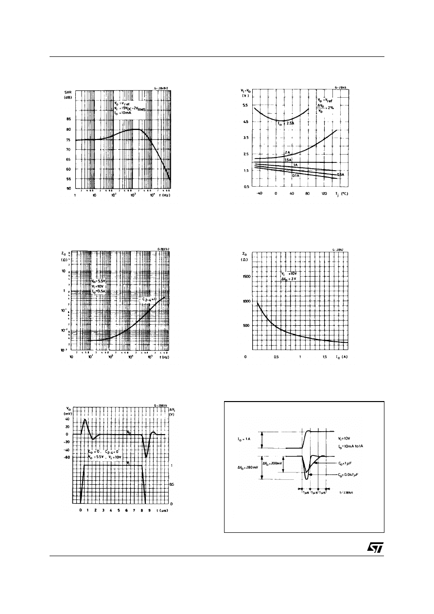
Figure 11. Supply Voltage Rejection vs.
Frequency.
Figure 12. Dropout Voltage vs. Junction
Temperature.
Fi g ure 13 . Ou t pu t Imped ance vs.
Frequency.
Figure 14. Output Impedance vs. Output
Current.
Figure 15. Voltage Transient Reponse.
Figure 16. Load Transient Reponse.
6/12
L200
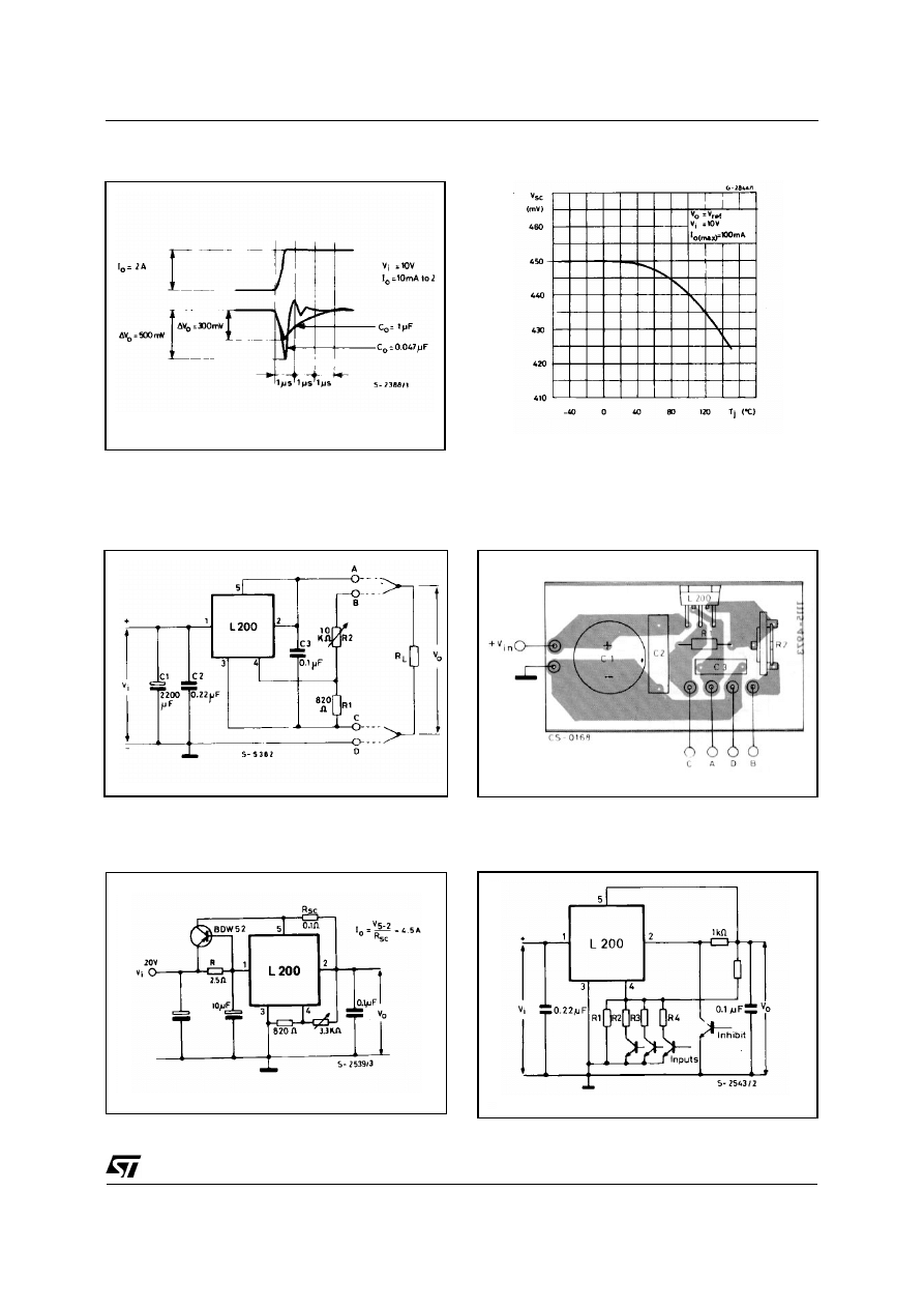
Figure 17. Load Transient Reponse
Figure 19. - Programmable Voltage Regulator
Figure 18. Current Limit Sense Voltage vs.
Junction Temperature.
Figure 20. - P.C. Board and Components Layout
of Figure 19.
Figure 21. - High Current Voltage Regulator with
Short Circuit Protection.
Figure 22. - Digitally Selected Regulator with
Inhibit.
APPLICATIONS CIRCUITS
7/12
L200
8/12
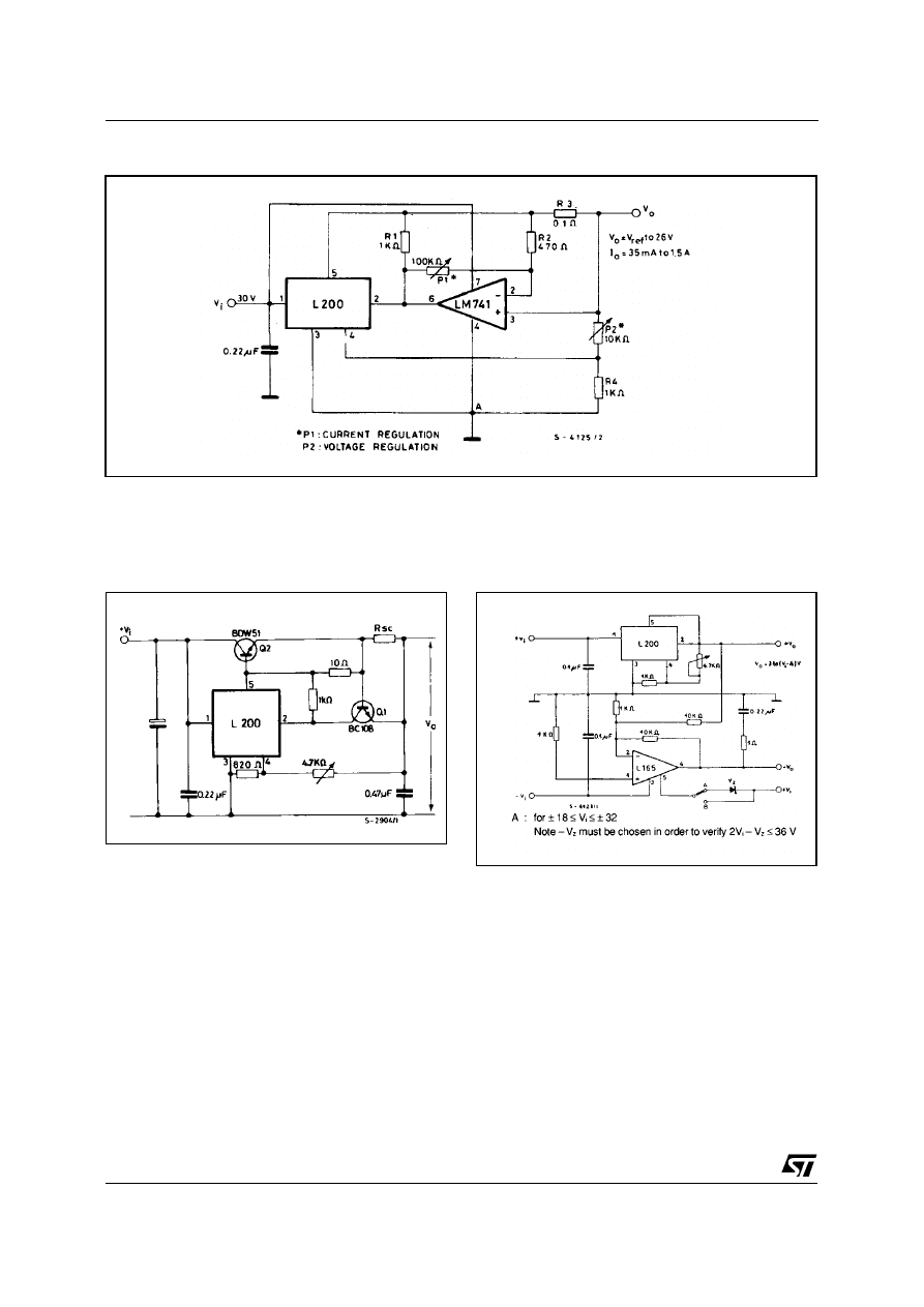
Figure 23. Programmable Voltage and Current Regulator.
Note: Connecting point A to a negative voltage (for example - 3V/10 mA) it is possible to extend the output voltage
range down to 0 V and obtain the current limiting down to this level (output short-circuit condition).
Figure 24. High Current Regulator with NPN
Pass Transistor.
Figure 25. High Current Tracking Regualtor.
L200
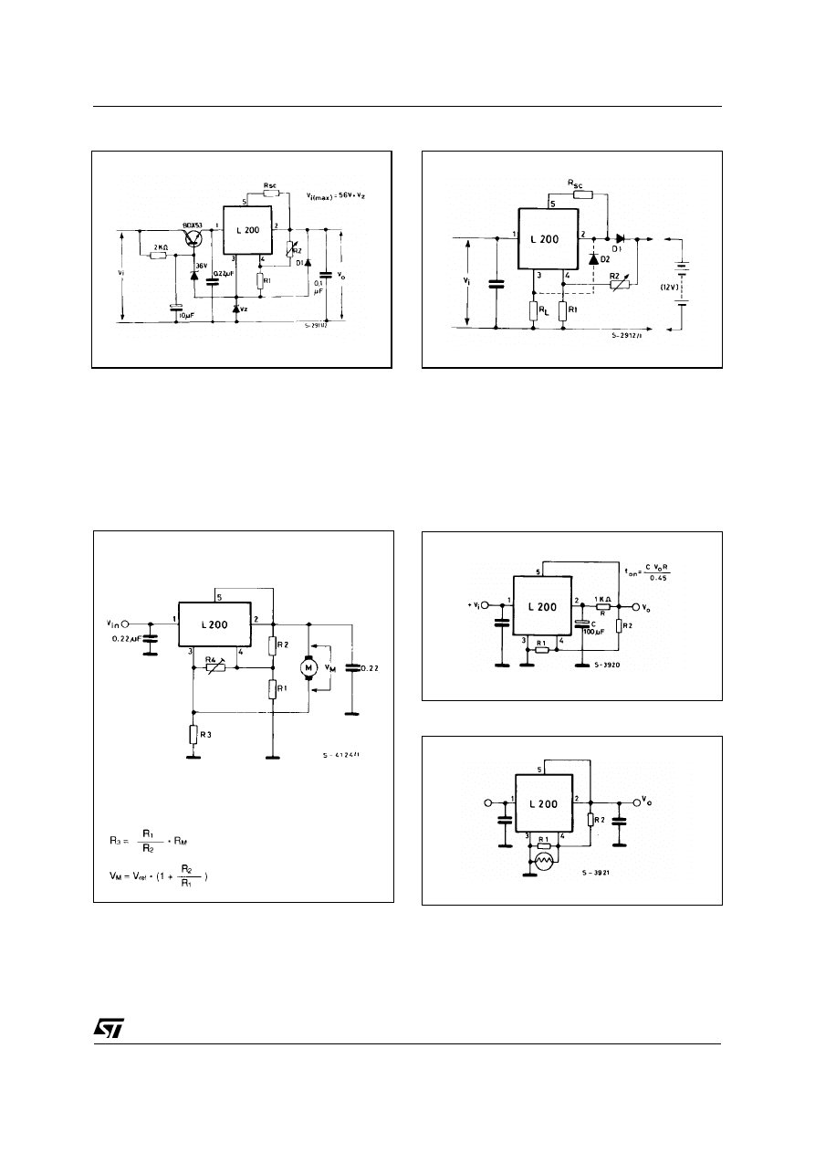
Figure 26. High Input and Output Voltage.
Figure 28. 30 W Motor Speed Control.
Figure 27. Constant Current Battery Charger.
Figure 29. Loww Turn on.
Figure 30. Light Controller.
The resistors R
1
and R
2
determine the final charging volt-
age and R
SC
the initial charging current. D
1
prevents dis-
charge of the battery throught the regulator.
The resistor RL limits the reverse currents through ther
regulator (which should be 100 mA max) when the bat-
tery is accidentally reverse connected. If R
L
is in series
with a bulb of 12 V/50 mA rating this will indicate incor-
rect connection.
9/12
L200
10/12
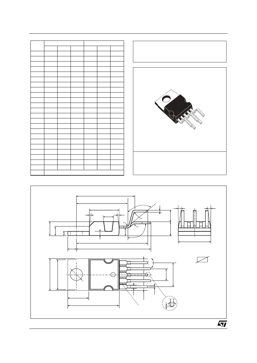
Pentawatt V
DIM.
mm
inch
MIN.
TYP.
MAX.
MIN.
TYP.
MAX.
A
4.8
0.189
C
1.37
0.054
D
2.4
2.8
0.094
0.110
D1
1.2
1.35
0.047
0.053
E
0.35
0.55
0.014
0.022
E1
0.76
1.19
0.030
0.047
F
0.8
1.05
0.031
0.041
F1
1
1.4
0.039
0.055
G
3.2
3.4
3.6
0.126
0.134
0.142
G1
6.6
6.8
7
0.260
0.268
0.276
H2
10.4
0.409
H3
10.05
10.4
0.396
0.409
L
17.55
17.85
18.15
0.691
0.703
0.715
L1
15.55
15.75
15.95
0.612
0.620
0.628
L2
21.2
21.4
21.6
0.831
0.843
0.850
L3
22.3
22.5
22.7
0.878
0.886
0.894
L4
1.29
0.051
L5
2.6
3
0.102
0.118
L6
15.1
15.8
0.594
0.622
L7
6
6.6
0.236
0.260
L9
0.2
0.008
M
4.23
4.5
4.75
0.167
0.177
0.187
M1
3.75
4
4.25
0.148
0.157
0.167
V4
40˚ (typ.)
L
L1
A
C
L5
D1
L2
L3
E
M1
M
D
H3
Dia.
L7
L6
F1
H2
F
G G1
E1
F
E
L9
V4
R
R
R
RESIN BETWEEN
LEADS
H1
V3
H2
L8
V
V
V1
B
V
V
V4
V4
OUTLINE AND
MECHANICAL DATA
L200
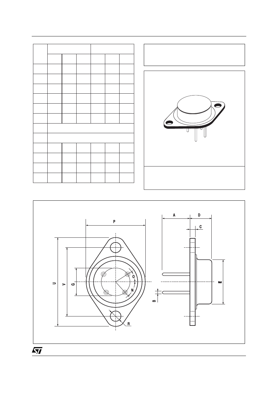
TO3 4-Leads
DIM.
mm
inch
MIN.
TYP.
MAX.
MIN.
TYP.
MAX.
A
11.8
0.46
B (*)
1
0.39
C
2.5
0.098
D
9.6
0.37
E
20
0.78
G
12.7
0.50
N
50
°
(typ.)
O
30
°
(typ.)
P
26.2
1.03
R
3.88
4.20
0.15
0.16
U
39.5
1.55
V
30.1
1.18
(*) Measured with Gauge
OUTLINE AND
MECHANICAL DATA
11/12
L200

12/12
Information furnished is believed to be accurate and reliable. However, STMicroelectronics assumes no responsibility for the consequences of
use of such information nor for any infringement of patents or other rights of third parties which may result from its use. No license is granted
by implication or otherwise under any patent or patent rights of STMicroelectronics. Specification mentioned in this publication are subject to
change without notice. This publication supersedes and replaces all information previously supplied. STMicroelectronics products are not
authorized for use as critical components in life support devices or systems without express written approval of STMicroelectronics.
The ST logo is a registered trademark of STMicroelectronics
© 2000 STMicroelectronics – Printed in Italy – All Rights Reserved
STMicroelectronics GROUP OF COMPANIES
Australia - Brazil - China - Finland - France - Germany - Hong Kong - India - Italy - Japan - Malaysia - Malta - Morocco -
Singapore - Spain - Sweden - Switzerland - United Kingdom - U.S.A.
http://www.st.com
L200

This datasheet has been download from:
Datasheets for electronics components.
Wyszukiwarka
Podobne podstrony:
Impulsowy regulator mocy DC id Nieznany
Badanie napiecia wstepnego id 7 Nieznany (2)
Napiecie powierzchniowe id 3136 Nieznany
LACZNIKI WYSOKIEGO NAPIECIA id Nieznany
Pomiary napiec zmiennych id 374 Nieznany
Dobor parametrow regulatora id Nieznany
PA UCHYB USTAKONY REGULACJI id Nieznany
balun napieciowy pradowy id 791 Nieznany (2)
Napiecie powierz id 313676 Nieznany
Badanie regulatorow ciaglych id Nieznany
pomiar napiecia stalego id 3738 Nieznany
cw 16 odpowiedzi do pytan id 1 Nieznany
Opracowanie FINAL miniaturka id Nieznany
How to read the equine ECG id 2 Nieznany
PNADD523 USAID SARi Report id 3 Nieznany
OPERAT STABLE VERSION ugoda id Nieznany
biuletyn katechetyczny pdf id 8 Nieznany
Finanse publiczne cw 4 E S id 1 Nieznany
więcej podobnych podstron