HCC/HCF4034B
INPUT/OUTPUT BUS REGISTER
8-STAGE STATIC BIDIRECTIONAL PARALLEL/SERIAL
DESCRIPTION
.
BIDIRECTIONAL PARALLEL DATA INPUT
.
PARALLEL OR SERIAL INPUTS/PARALLEL
OUTPUTS
.
ASYNCHRONOUS OR SYNCHRONOUS PAR-
ALLEL DATA LOADING
.
PARALLEL DATA-INPUT ENABLE ON ”A”
DATA LINES (3-state output)
.
DATA RECIRCULATION FOR REGISTER EX-
PANSION
.
MULTIPACKAGE REGISTER EXPANSION
.
FULLY STATIC OPERATIONAL DC-TO-5MHz
(typ.) AT V
DD
= 10V
.
QUIESCENT CURRENT SPECIFIED TO 20V
FOR HCC DEVICE
.
5V, 10V, AND 15V PARAMETRIC RATINGS
.
INPUT CURRENT OF 100nA AT 18V AND 25
°
C
FOR HCC DEVICE
.
100% TESTED FOR QUIESCENT CURRENT
.
MEETS ALL REQUIREMENTS OF JEDEC TEN-
TATIVE STANDARD N
°
13A, ”STANDARD SPE-
CIFICATIONS FOR DESCRIPTION OF ”B”
SERIES CMOS DEVICES”
June 1989
The HCC4034B (extended temperature range) and
HCF4034B (intermediate temperature range) are
monolithic integrated circuits, available in 24-lead
dual in-line plastic or ceramic package and plastic
micro package. The HCC/HCF4034B is a static
eight-stage parallel-or serial-input parallel-output
register. It can be used to : 1) bidirectionally transfer
parallel information between two buses ; 2) convert
serial data to parallel form and direct the parallel
data to either of two buses ; 3) store (recirculate) par-
allel data, or 4) accept parallel data from either of two
buses and convert that data to serial form. Inputs
that control the operations include a single-phase
CLOCK (CL), A DATA ENABLE (AE), ASYN-
CHRONOUS/SYNCHRONOUS (A/S), A-BUS-TO-
B-BUS/B-BUS-TO-A-BUS (A/B), and PARALLEL/
SERIAL (P/S). Data inputs include 16 bidirectional
parallel data lines of which the eight A data lines are
inputs (3-state outputs) and the B data lines are out-
puts (inputs) depending on the signal level on the
A/B input. In addition, an input for SERIAL DATA is
also provided. All register stages are D-type master-
slave flip-flops with separate master and slave clock
EY
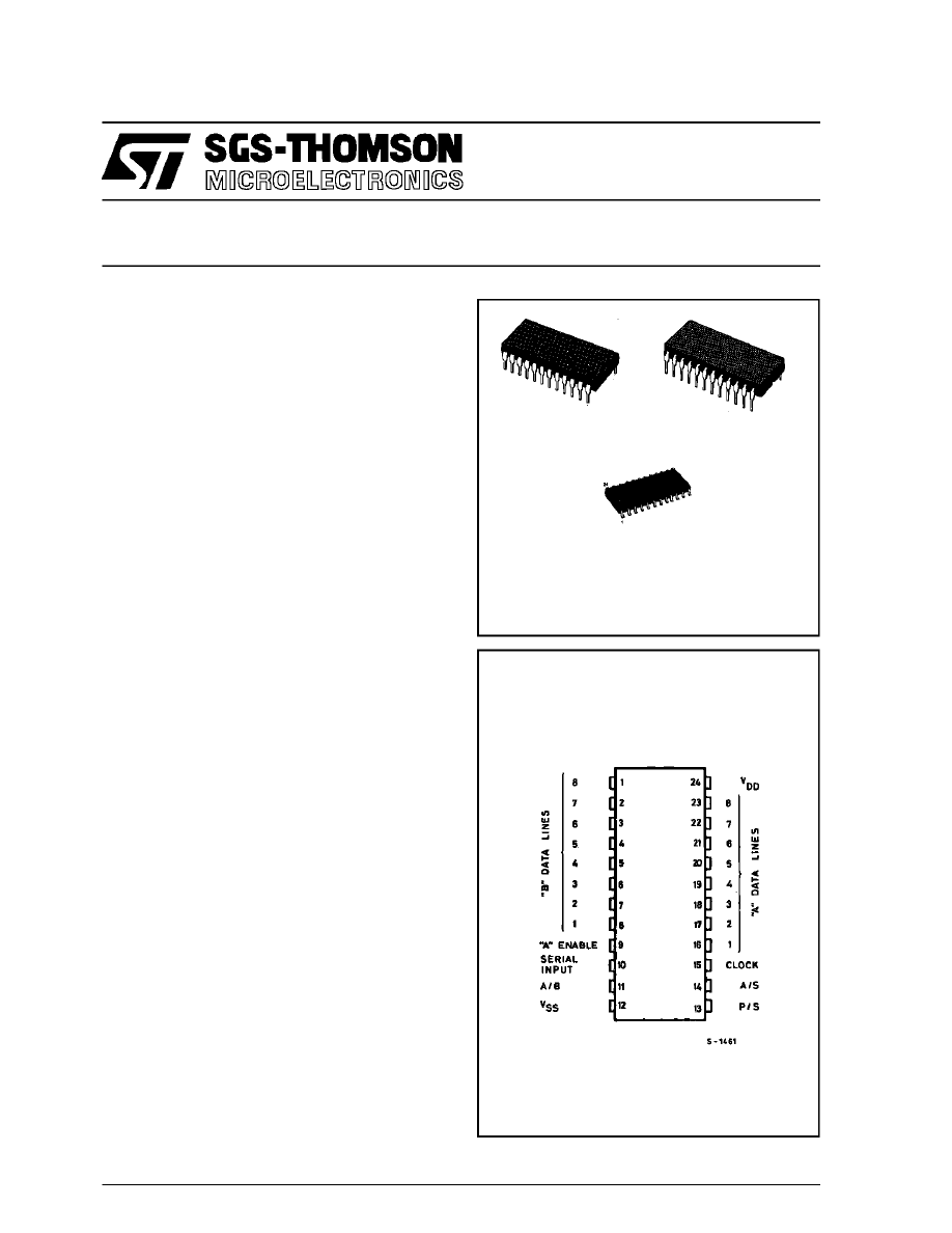
(Plastic Package)
F
(Ceramic Frit Seal Package)
M1
(Micro Package)
ORDER CODES :
HCC4034BF
HCF4034BEY
HCF4034BM1
PIN CONNECTIONS
1/16
inputs generated internally to allow synchronous or
asynchronous data transfer from master to slave.
Isolation from external noise and the effects of load-
ing is provided by output buffering.
PARALLEL OPERATION – A high P/S input signal
allows data transfer into the register via the parallel
data lines synchronously with the positive transition
of the clock provided the A/S input is low. If the A/S
input is high the transfer is independent of the clock.
The direction of data flow is controlled by the A/B
input. When this signal is high the A data lines are
inputs (and B data lines are outputs) ; a low A/B sig-
nal reverses the direction of data flow. The AE-input
is an additional feature which allows many registers
to feed data to a common bus. The A DATA lines are
enabled only when this signal is high. Data storage
through recirculation of data in each register stage
is accomplished by making the A/B signal high and
the AE signal low.
SERIALOPERATION – A low P/S signal allows ser-
ial data to transfer into the register synchronously
with the positive transition of the clock. The A/S input
is internally disabled when the register is in the serial
mode (asynchronous
serial operation
is not
allowed). The serial data appears as output data on
either the B lines (when A/B is high) or the A lines
(when A/B is low and the AE signal is high). Register
expansion can be accomplished by simply cascad-
ing HCC/HCF4034B packages.
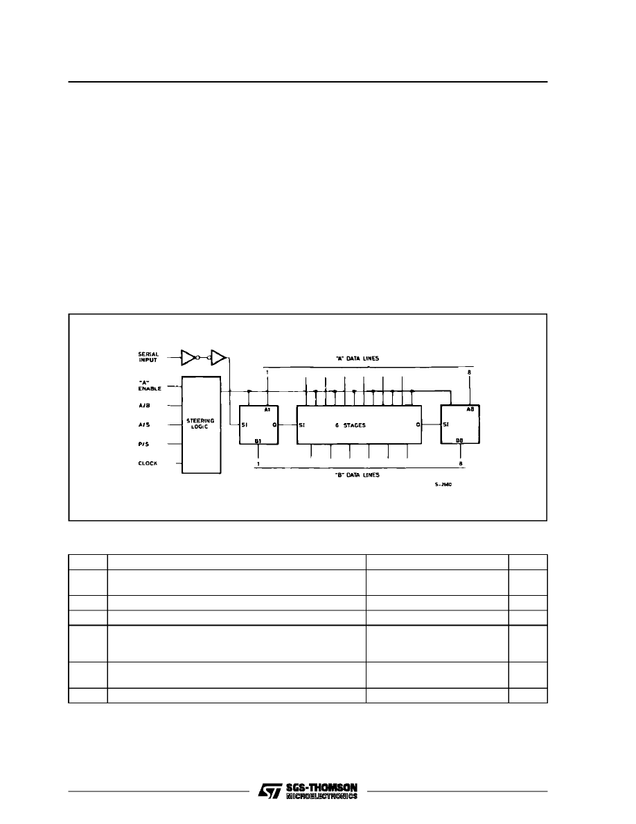
FUNCTIONAL DIAGRAM
ABSOLUTE MAXIMUM RATINGS
Symbol
Parameter
Value
Unit
V
DD
*
Supply Voltage : HCC Types
HCF Types
– 0.5 to + 20
– 0.5 to + 18
V
V
V
i
Input Voltage
– 0.5 to V
DD
+ 0.5
V
I
I
DC Input Current (any one input)
±
10
mA
P
tot
Total Power Dissipation (per package)
Dissipation per Output Transistor
for T
op
= Full Package-temperature Range
200
100
mW
mW
T
op
Operating Temperature : HCC Types
HCF Types
– 55 to + 125
– 40 to + 85
°
C
°
C
T
s tg
Storage Temperature
– 65 to + 150
°
C
Stresses above those listed under ”Absolute Maximum Ratings” may cause permanent damage to the device. This is a stress
rating only and functional operation of the device at these or any other conditions above those indicated in the operational sec-
tions of this specifi cation is not implied. Exposure to absolute maximum rating conditions for external periods may affect device
reliability.
HCC/HCF4034B
2/16
RECOMMENDED OPERATING CONDITIONS
Symbol
Parameter
Value
Unit
V
DD
Supply Voltage : HCC Types
HCF Types
3 to 18
3 to 15
V
V
V
I
Input Voltage
0 to V
DD
V
T
op
Operating Temperature : HCC Types
HCF Types
– 55 to + 125
– 40 to + 85
°
C
°
C
LOGIC DIAGRAMS
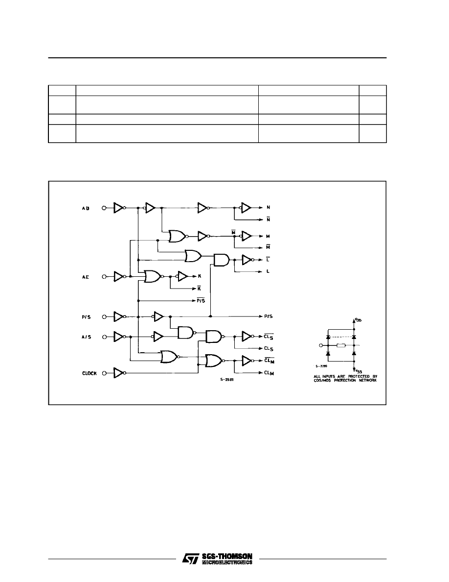
STEERING LOGIC
HCC/HCF4034B
3/16
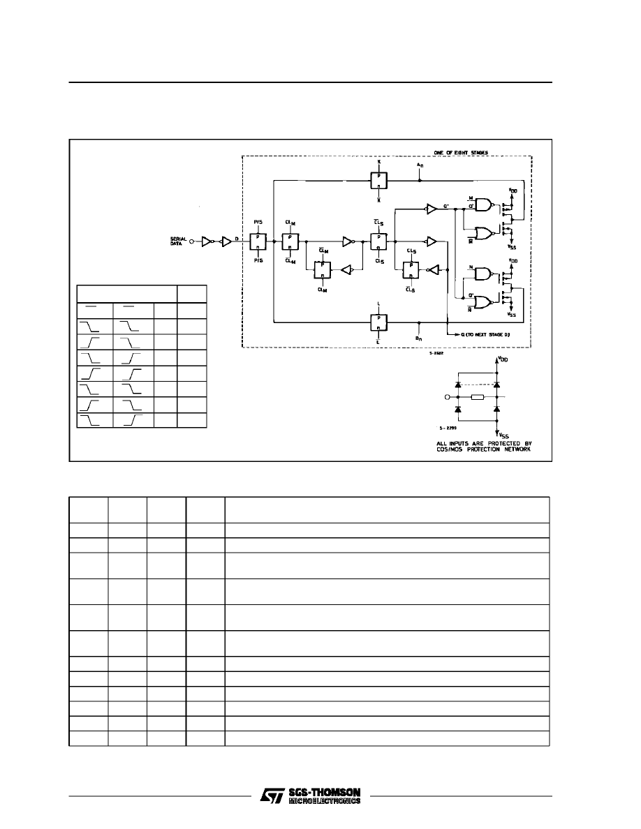
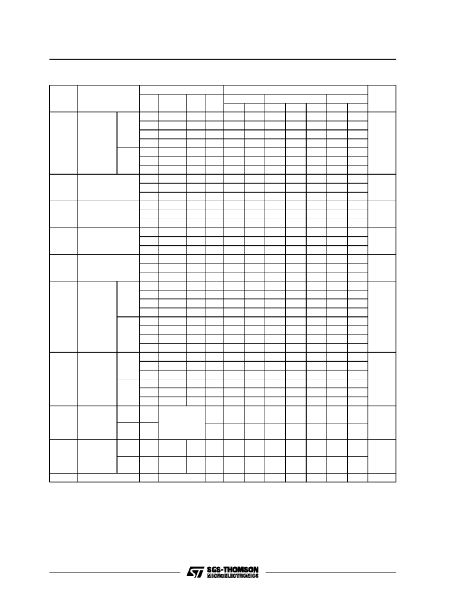
LOGIC DIAGRAM AND TRUTH TABLE
▲
= LEVEL CHANGE
•
=
INVALID CONDI-
INPUTS
OUT
CL
M
▲
CL
S
▲
D
Q
0
0
0
0
0
•
X
0
1
1
1
1
1
•
FOR REGISTER INPUT-LEVELS AND RESULTING REGISTER OPERATION
”A”
Enable
P/S
A/B
A/S
Operation*
0
0
0
X
Serial Mode ; Synch. Serial Data Input, ”A” Parallel Data Outputs Disabled
0
0
1
X
Serial Mode ; Synch. Serial Data Input, ”B” Parallel Data Output
0
1
0
0
Parallel Mode ; ”B” Synch. Parallel Data Inputs, ”A” Parallel Data Outputs
Disabled
0
1
0
1
Parallel Mode ; ”B” Asynch. Parallel Data Inputs, ”A” Parallel Data Outputs
Disabled
0
1
1
0
Parallel Mode ; ”A” Parallel Data Inputs Disabled, ”B” Parallel Data Outputs,
Synch. Data Recirculation
0
1
1
1
Parallel Mode ; ”A” Parallel Data Inputs Disabled, ”B” Parallel Data Outputs,
Asynch. Data Recirculation
1
0
0
X
Serial Mode ; Synch. Serial Data Input, ”A” Parallel Data Output
1
0
1
X
Serial Mode ; Synch. Serial Data Input, ”B” Parallel Data Output
1
1
0
0
Parallel Mode ; ”B” Synch. Parallel Data Input, ”A” Parallel Data Output
1
1
0
1
Parallel Mode ; ”B” Asynch. Parallel Data Input, ”A” Parallel Data Output
1
1
1
0
Parallel Mode ; ”A” Synch. Parallel Data Input, ”B” Parallel Data Output
1
1
1
1
Parallel Mode ; ”A” Asynch. Parallel Data Input, ”B” Parallel Data Outpu
* Outputs change at positive transition of clock in the serial mode and when the A/S control inputs is ”low” in the parallel
mode.
REGISTER STAGE (1 of 8 stages)
HCC/HCF4034B
4/16
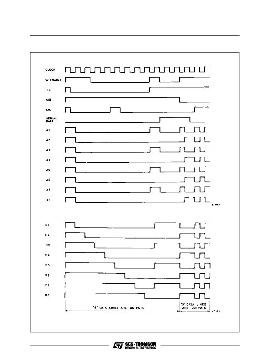
TIMING DIAGRAM
HCC/HCF4034B
5/16
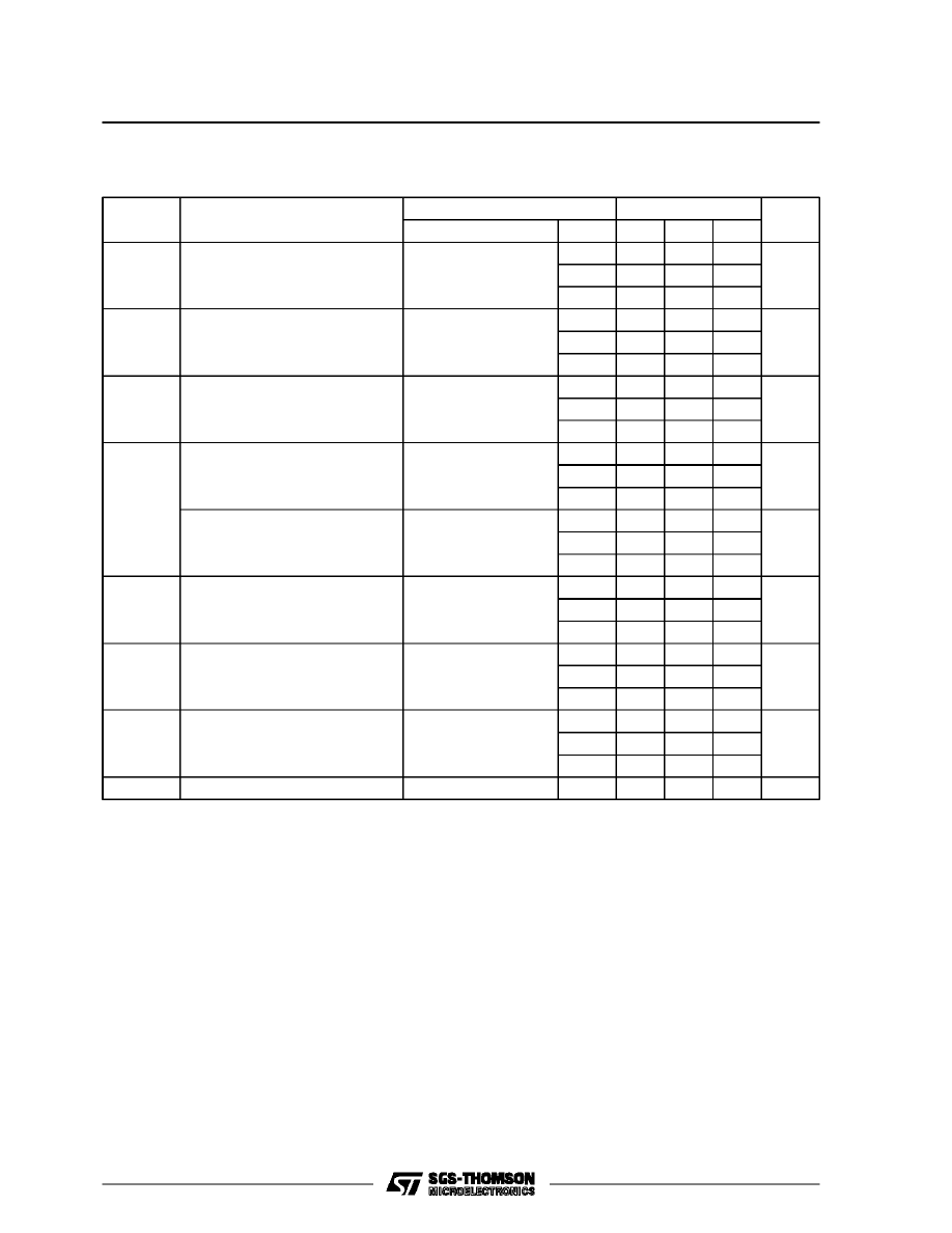
STATIC ELECTRICAL CHARACTERISTICS (over recommended operating conditions)
Test Conditions
Values
V
I
V
O
|I
O
|
V
DD
T
Low
*
25
°
C
T
Hi gh
*
Symbol
Parameter
(V)
(V)
(
µ
A)
(V)
Min.
Max.
Min.
Typ. Max.
Min.
Max.
Unit
I
L
Quiescent
Current
HCC
Types
0/ 5
5
5
0.04
5
150
µ
A
0/10
10
10
0.04
10
300
0/15
15
20
0.04
20
600
0/20
20
100
0.08
100
3000
HCF
Types
0/ 5
5
20
0.04
20
150
0/10
10
40
0.04
40
300
0/15
15
80
0.04
80
600
V
OH
Output High
Voltage
0/ 5
< 1
5
4.95
4.95
4.95
V
0/10
< 1
10
9.95
9.95
9.95
0/15
< 1
15
14.95
14.95
14.95
V
OL
Output Low
Voltage
5/0
< 1
5
0.05
0.05
0.05
V
10/0
< 1
10
0.05
0.05
0.05
15/0
< 1
15
0.05
0.05
0.05
V
IH
Input High
Voltage
0.5/4.5
< 1
5
3.5
3.5
3.5
V
1/9
< 1
10
7
7
7
1.5/13.5
< 1
15
11
11
11
V
IL
Input Low
Voltage
4.5/0.5
< 1
5
1.5
1.5
1.5
V
9/1
< 1
10
3
3
3
13.5/1.5
< 1
15
4
4
4
I
OH
Output
Drive
Current
HCC
Types
0/ 5
2.5
5
– 2
– 1.6 – 3.2
– 1.15
mA
0/ 5
4.6
5
– 0.64
– 0.51
– 1
– 0.36
0/10
9.5
10
– 1.6
– 1.3 – 2.6
– 0.9
0/15
13.5
15
– 4.2
– 3.4 – 6.8
– 2.4
HCF
Types
0/ 5
2.5
5
– 1.53
– 1.36 – 3.2
– 1.1
0/ 5
4.6
5
– 0.52
– 0.44
– 1
– 0.36
0/10
9.5
10
– 1.3
– 1.1 – 2.6
– 0.9
0/15
13.5
15
– 3.6
– 3.0 – 6.8
– 2.4
I
OL
Output
Sink
Current
HCC
Types
0/ 5
0.4
5
0.64
0.51
1
0.36
mA
0/10
0.5
10
1.6
1.3
2.6
0.9
0/15
1.5
15
4.2
3.4
6.8
2.4
HCF
Types
0/ 5
0.4
5
0.52
0.44
1
0.36
0/10
0.5
10
1.3
1.1
2.6
0.9
0/15
1.5
15
3.6
3.0
6.8
2.4
I
IH
, I
IL
Input
Leakage
Current
HCC
Types
0/18
Any Input
18
±
0.1
±
10
–5
±
0.1
±
1
µ
A
HCF
Types
0/15
15
±
0.3
±
10
–5
±
0.3
±
1
I
OH
3-State
Output
Leakage
Current
HCC
Types
0/18
0/18
18
±
0.4
±
10
–4
±
0.4
±
12
µ
A
HCF
Types
0/15
0/15
15
±
1.0
±
10
–4
±
1.0
±
7.5
C
I
Input Capacitance
Any Input
5
7.5
pF
* T
Lo w
=
– 55
°
C for HCC device : – 40
°
C for HCF device.
* T
High
=
+ 125
°
C for HCC device : + 85
°
C for HCF device.
The Noise Margin for both ”1” and ”0” level is : 1V min. with V
DD
= 5V, 2V min. with V
DD
= 10V, 2.5V min. with V
DD
= 15V.
HCC/HCF4034B
6/16
DYNAMIC ELECTRICAL CHARACTERISTICS (T
amb
= 25
°
C, C
L
= 50pF, R
L
= 200k
Ω
,
typical temperature coefficient for all V
DD
values is 0.3%/
°
C, all input rise and fall times = 20ns)
Test Conditions
Value
Symbol
Parameter
V
DD
(V)
Min.
Typ.
Max.
Unit
t
PHL
, t
PLH
Propagation Delay Time :
A (B) Parallel Data in to
B (A) Parallel Data Out
5
350
700
ns
10
120
240
15
85
170
t
PLZ
, t
PHZ
t
PZ L
, t
PZ H
3-state Propagation Delay Time
A/B or AE to ”A” OUT
5
200
400
ns
10
80
160
15
60
120
t
THL
, t
T LH
Transition Time
5
100
200
ns
10
50
100
15
40
80
t
s etu p
Data Setup Time Serial Data to
Clock
5
80
160
ns
10
30
60
15
20
40
Parallel Data to Clock
5
25
50
ns
10
15
30
15
10
20
t
w
High-level Pulse Width, AE, P/S,
A/S
5
175
350
ns
10
70
140
15
40
80
f
CL
Maximum Clock Frequency
5
2
4
MHz
10
5
10
15
7
14
t
W
Clock Pulse Width
5
125
250
ns
10
50
100
15
35
70
t
r
, t
f
*
Clock Input Rise or Fall Time
5,10,15
15
µ
s
* If more than one unit is cascaded. t
r
should be made less than or equal to the sum of the transition time and the fixed propagation delay of the
output of the driving stage for the estimated capacitive load.
HCC/HCF4034B
7/16
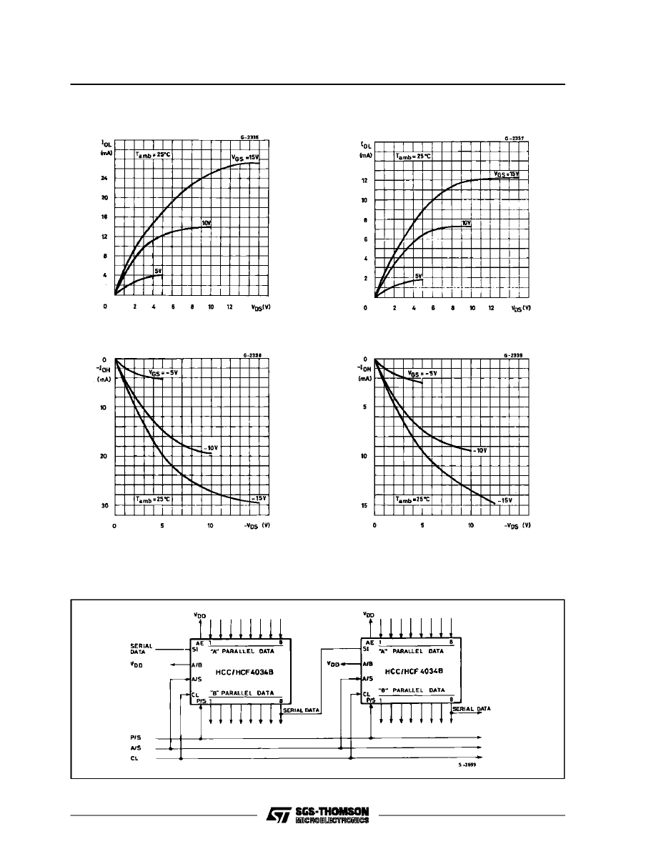
Typical Output Low (sink) Current Characteristics.
Minimum Output Low (sink) Current
Charac-
teristics.
Typical Output High (source) Current Charac-
teristics.
Minimum Output High (source) Current Charac-
teristics.
TYPICAL APPLICATIONS
16-BIT PARALLEL IN/PARALLEL OUT PARALLEL IN/SERIAL OUT, SERIAL IN/PARALLEL OUT, SERIAL
IN/SERIAL OUT REGISTER.
HCC/HCF4034B
8/16
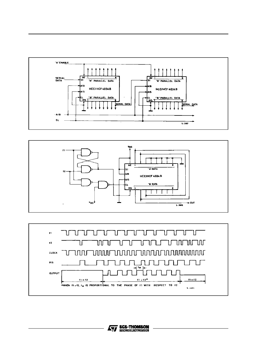
FREQUENCY AND PHASE COMPARATOR.
TYPICAL APPLICATIONS (continued)
16-BIT SERIAL IN/GATED PARALLEL OUT REGISTER
TIMING DIAGRAM
HCC/HCF4034B
9/16
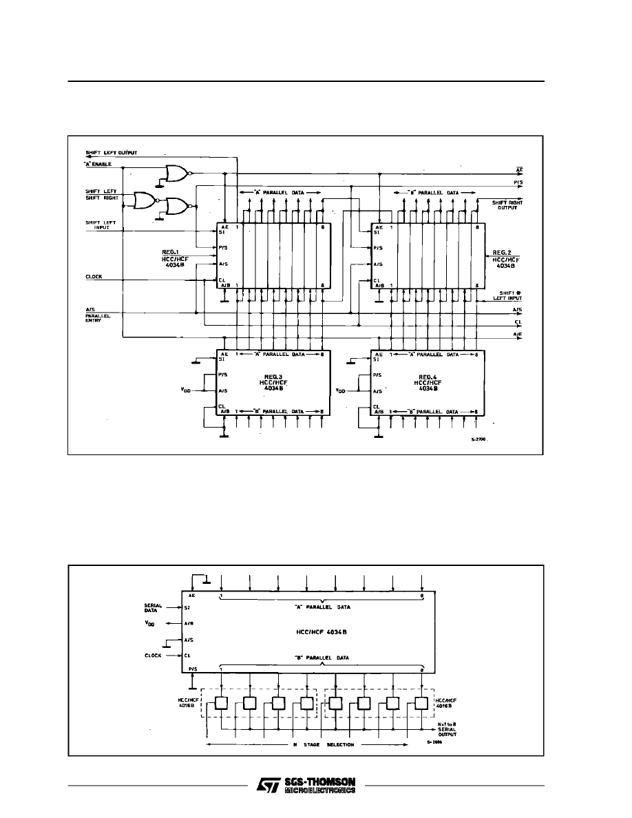
SHIFT RIGHT/SHIFT LEFT WITH PARALLEL INPUTS
A ”High” (”Low”) on the Shift Left/Shift Right input
allows serial data on the Shift Left Input (Shift Right
Input) to enter the register on the positive transition
of the clock signal. A ”high” on the ”A” Enable Input
disables the ”A” parallel data lines on Reg. 1 and 2
and enables the ”A” data lines on registers 3 and 4
and allows parallel data into registers 1 and 2. Other
logic schemes may be used in place of registers 3
and 4 for parallel loading. When parallel inputs are
not used Reg. 3 and 4 and associated logic are not
required.
* Shift Left input must be disabled during parallel
entry.
N-STAGE REGISTER WITH FIXED SERIAL OUTPUT LINE
TYPICAL APPLICATIONS (continued)
HCC/HCF4034B
10/16
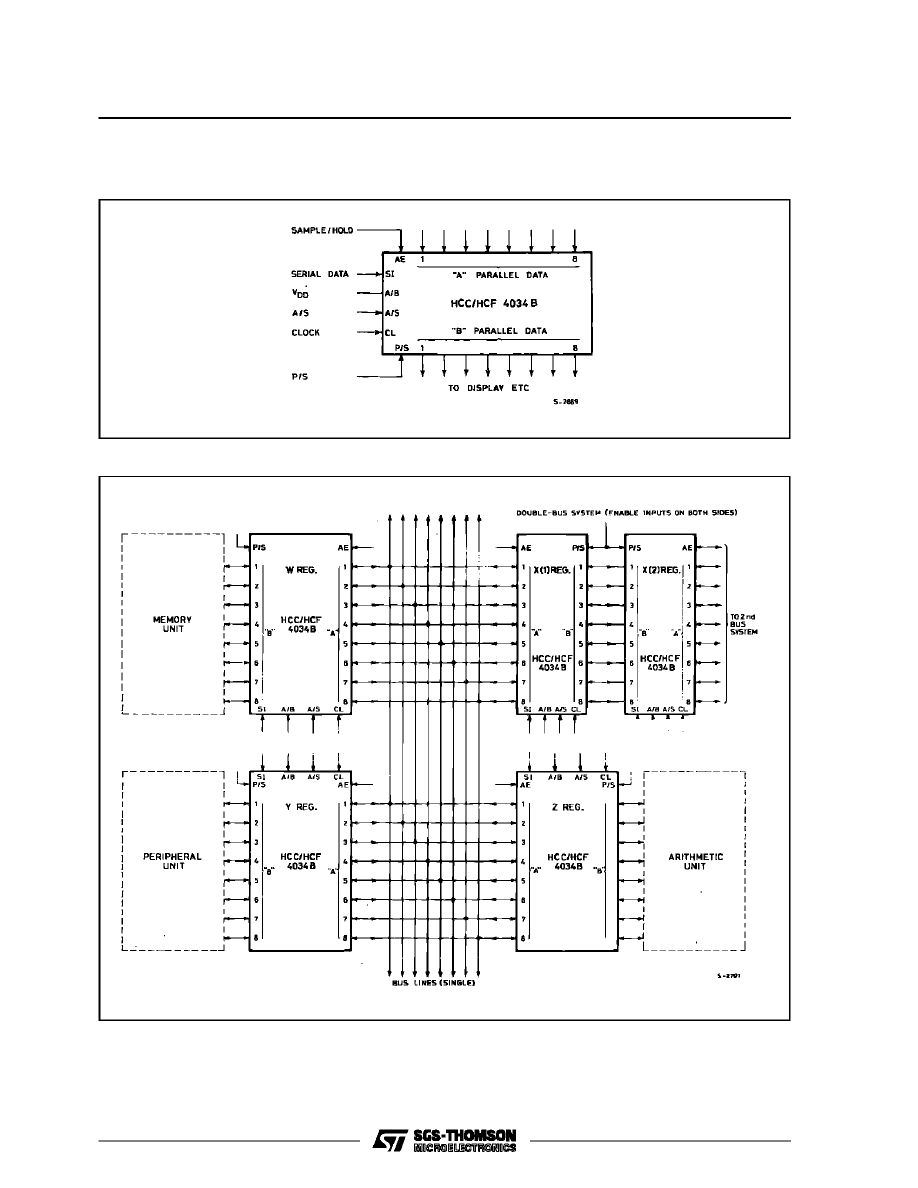
SAMPLE AND HOLD REGISTER-SERIAL/PARALLEL IN-PARALLEL OUT
TYPICAL APPLICATIONS (continued)
SINGLE-AND DOUBLE-BUS SYSTEMS
The ”A” enable (AE) and A/B signals control all combinations of transfer between the registers and bus systems.
HCC/HCF4034B
11/16
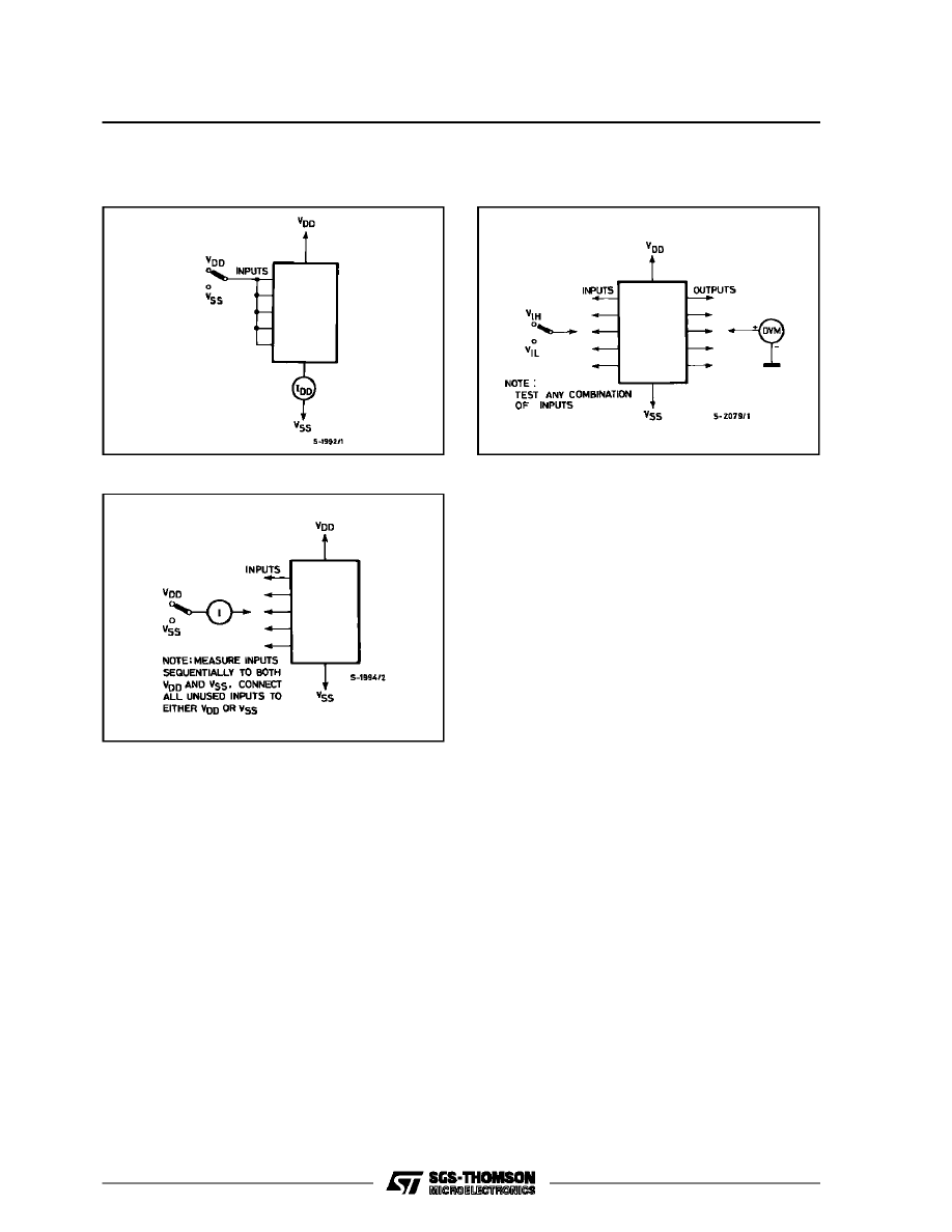
Noise Immunity.
TEST CIRCUITS
Quiescent Device Current.
Input Leakage Current.
HCC/HCF4034B
12/16
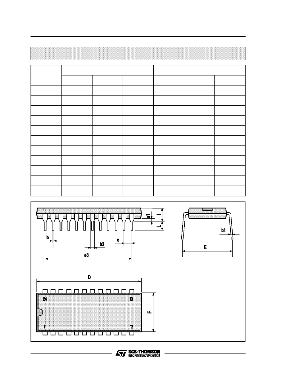
Plastic DIP24 (0.25) MECHANICAL DATA
DIM.
mm
inch
MIN.
TYP.
MAX.
MIN.
TYP.
MAX.
a1
0.63
0.025
b
0.45
0.018
b1
0.23
0.31
0.009
0.012
b2
1.27
0.050
D
32.2
1.268
E
15.2
16.68
0.598
0.657
e
2.54
0.100
e3
27.94
1.100
F
14.1
0.555
I
4.445
0.175
L
3.3
0.130
P043A
HCC/HCF4034B
13/16
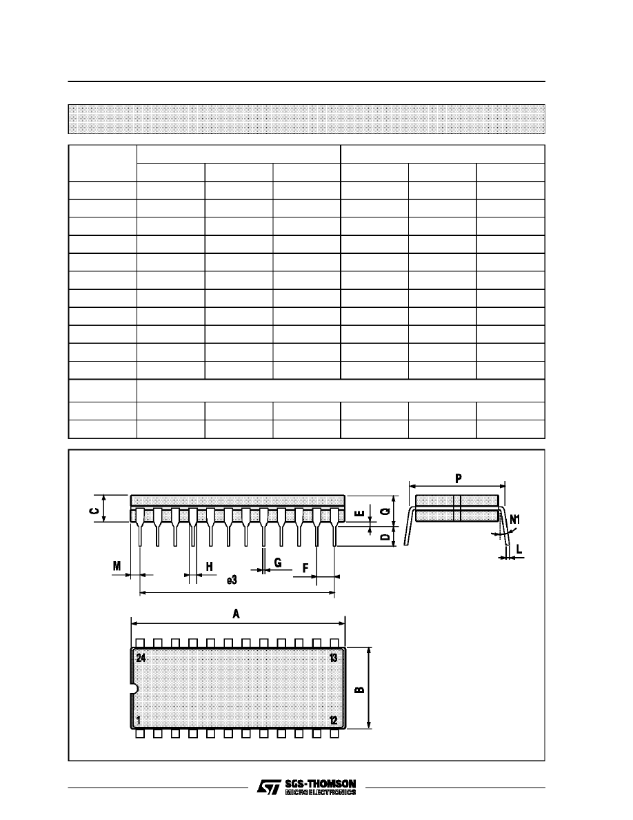
Ceramic DIP24 MECHANICAL DATA
DIM.
mm
inch
MIN.
TYP.
MAX.
MIN.
TYP.
MAX.
A
32.3
1.272
B
13.05
13.36
0.514
0.526
C
3.9
5.08
0.154
0.200
D
3
0.118
E
0.5
1.78
0.020
0.070
e3
27.94
1.100
F
2.29
2.79
0.090
0.110
G
0.4
0.55
0.016
0.022
I
1.17
1.52
0.046
0.060
L
0.22
0.31
0.009
0.012
M
1.52
2.49
0.060
0.098
N1
4
°
(min.), 15
°
(max.)
P
15.4
15.8
0.606
0.622
Q
5.71
0.225
P058C
HCC/HCF4034B
14/16
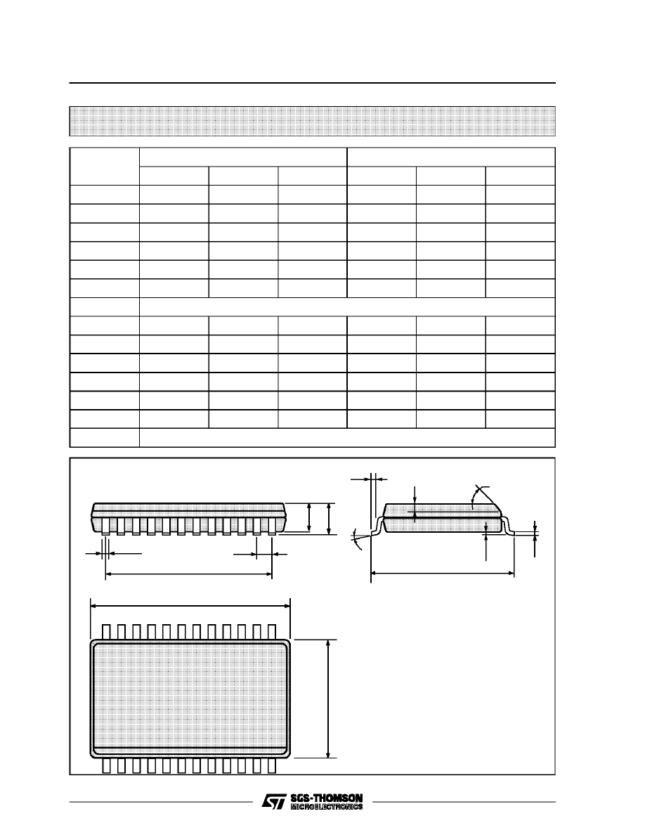
SO24 MECHANICAL DATA
DIM.
mm
inch
MIN.
TYP.
MAX.
MIN.
TYP.
MAX.
A
2.65
0.104
a1
0.10
0.20
0.004
0.007
a2
2.45
0.096
b
0.35
0.49
0.013
0.019
b1
0.23
0.32
0.009
0.012
C
0.50
0.020
c1
45
°
(typ.)
D
15.20
15.60
0.598
0.614
E
10.00
10.65
0.393
0.420
e
1.27
0.05
e3
13.97
0.55
F
7.40
7.60
0.291
0.299
L
0.50
1.27
0.19
0.050
S
8
°
(max.)
F
C
L
E
a1
b1
A
e
D
e3
b
24
13
1
12
c1
s
a2
HCC/HCF4034B
15/16

Information furnished is believed to be accurate and reliable. However, SGS-THOMSON Microelectronics assumes no responsability for the
consequences of use of such information nor for any infringement of patents or other rights of third parties which may results from its use. No
license is granted by implication or otherwise under any patent or patent rights of SGS-THOMSON Microelectronics. Specifications mentioned
in this publication are subject to change without notice. This publication supersedes and replaces all information previously supplied.
SGS-THOMSON Microelectronics products are not authorized for use as critical components in life support devices or systems without express
written approval of SGS-THOMSON Microelectonics.
1994 SGS-THOMSON Microelectronics - All Rights Reserved
SGS-THOMSON Microelectronics GROUP OF COMPANIES
Australia - Brazil - France - Germany - Hong Kong - Italy - Japan - Korea - Malaysia - Malta - Morocco - The Netherlands -
Singapore - Spain - Sweden - Switzerland - Taiwan - Thailand - United Kingdom - U.S.A
HCC/HCF4034B
16/16
Wyszukiwarka
Podobne podstrony:
4034
02Bid 4034 Nieznany
4034
4034 a
4034
4034
4034
4034
4034
4034
4034
4034
4034
4034
więcej podobnych podstron