© Semiconductor Components Industries, LLC, 2006
March, 2006 − Rev. 6
1
Publication Order Number:
MC14553B/D
MC14553B
3−Digit BCD Counter
The MC14553B 3−digit BCD counter consists of 3 negative edge
triggered BCD counters that are cascaded synchronously. A quad latch
at the output of each counter permits storage of any given count. The
information is then time division multiplexed, providing one BCD
number or digit at a time. Digit select outputs provide display control.
All outputs are TTL compatible.
An on−chip oscillator provides the low−frequency scanning clock
which drives the multiplexer output selector.
This device is used in instrumentation counters, clock displays,
digital panel meters, and as a building block for general logic
applications.
•
TTL Compatible Outputs
•
On−Chip Oscillator
•
Cascadable
•
Clock Disable Input
•
Pulse Shaping Permits Very Slow Rise Times on Input Clock
•
Output Latches
•
Master Reset
w
These devices are available in Pb−free package(s). Specifications herein
apply to both standard and Pb−free devices. Please see our website at
www.onsemi.com for specific Pb−free orderable part numbers, or
contact your local ON Semiconductor sales office or representative.
MAXIMUM RATINGS
(Voltages Referenced to V
SS
Symbol
Parameter
Value
Unit
V
DD
DC Supply Voltage Range
−0.5 to +18.0
V
V
in
, V
out
Input or Output Voltage Range
(DC or Transient)
−0.5 to V
DD
+ 0.5
V
I
in
Input Current
(DC or Transient) per Pin
±10
mA
I
out
Output Current
(DC or Transient) per Pin
+20
mA
P
D
Power Dissipation,
500
mW
T
A
Ambient Temperature Range
−55 to +125
°C
T
stg
Storage Temperature Range
−65 to +150
°C
T
L
Lead Temperature
(8−Second Soldering)
260
°C
1. Maximum Ratings are those values beyond which damage to the device
may occur.
2. Temperature Derating:
Plastic “P and D/DW” Packages: – 7.0 mW/_C From 65_C To 125_C
This device contains protection circuitry to guard against damage due to high
static voltages or electric fields. However, precautions must be taken to avoid
applications of any voltage higher than maximum rated voltages to this
high−impedance circuit. For proper operation, V
in
and V
out
should be constrained
to the range V
SS
v (V
in
or V
out
) v V
DD
.
Unused inputs must always be tied to an appropriate logic voltage level (e.g.,
either V
SS
or V
DD
). Unused outputs must be left open.
http://onsemi.com
A
= Assembly Location
WL, L
= Wafer Lot
YY, Y
= Year
WW, W = Work Week
Device
Package
Shipping
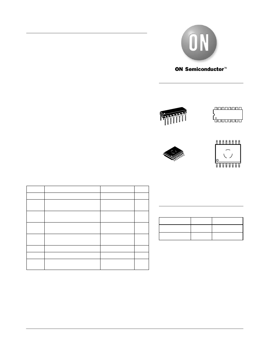
ORDERING INFORMATION
MC14553BCP
PDIP−16
25/Rail
MC14553BDW
SOIC−16
47/Rail
MARKING
DIAGRAMS
1
16
PDIP−16
P SUFFIX
CASE 648
MC14553BCP
AWLYYWW
SOIC−16
DW SUFFIX
CASE 751G
1
16
14553B
AWLYYWW
MC14553B
http://onsemi.com
2
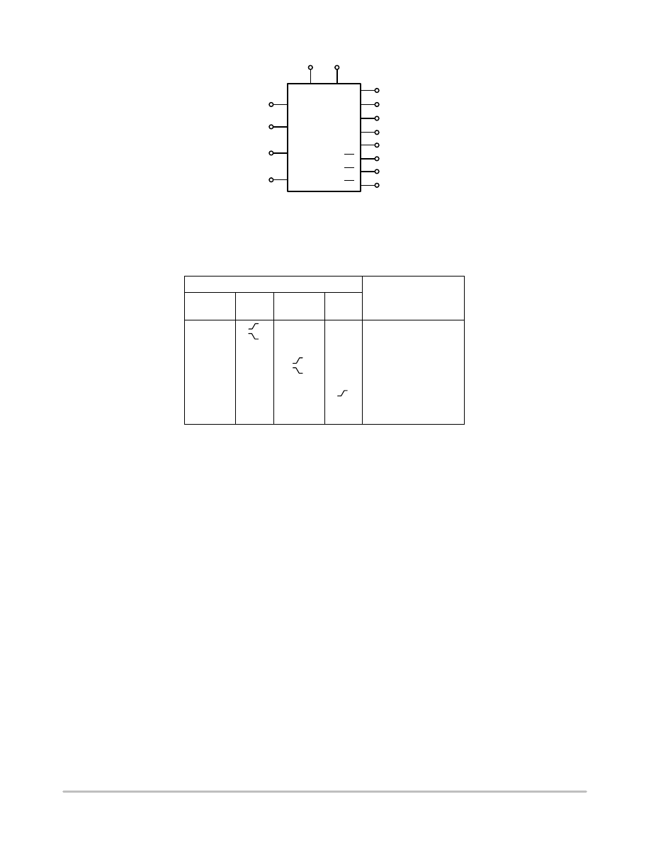
Figure 1. Block Diagram
12
10
11
13
9
7
6
5
14
2
1
15
V
DD
= PIN 16
V
SS
= PIN 8
4
3
CLOCK
LE
DIS
MR
Q0
Q1
Q2
Q3
O.F.
DS1
DS2
DS3
CIA
CIB
TRUTH TABLE
Inputs
Outputs
Master
Reset
Clock
Disable
LE
0
0
0
No Change
0
0
0
Advance
0
X
1
X
No Change
0
1
0
Advance
0
1
0
No Change
0
0
X
X
No Change
0
X
X
Latched
0
X
X
1
Latched
1
X
X
0
Q0 = Q1 = Q2 = Q3 = 0
X = Don’t Care
MC14553B
http://onsemi.com
3
ÎÎÎÎÎÎÎÎÎÎÎÎÎÎÎÎÎÎÎÎÎÎÎÎÎÎÎÎÎÎÎÎÎ
ÎÎÎÎÎÎÎÎÎÎÎÎÎÎÎÎÎÎÎÎÎÎÎÎÎÎÎÎÎÎÎÎÎ
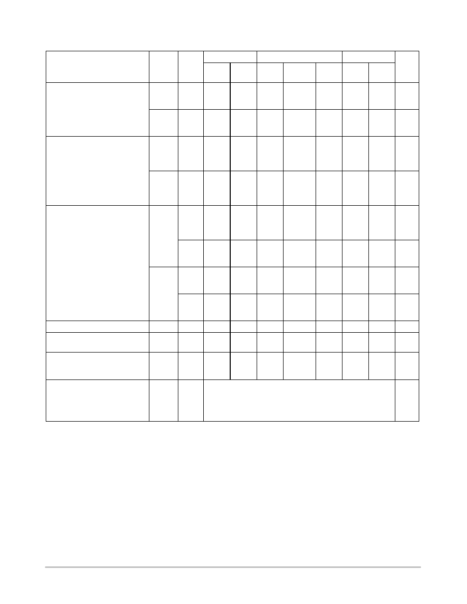
ELECTRICAL CHARACTERISTICS
(Voltages Referenced to V
SS
)
Characteristic
Symbol
V
DD
Vdc
− 55_C
25_C
125_C
Unit
Min
Max
Min
Typ
Max
Min
Max
Output Voltage
“0” Level
V
in
= V
DD
or 0
V
OL
5.0
10
15
—
—
—
0.05
0.05
0.05
—
—
—
0
0
0
0.05
0.05
0.05
—
—
—
0.05
0.05
0.05
Vdc
“1” Level
V
in
= 0 or V
DD
V
OH
5.0
10
15
4.95
9.95
14.95
—
—
—
4.95
9.95
14.95
5.0
10
15
—
—
—
4.95
9.95
14.95
—
—
—
Vdc
Input Voltage
“0” Level
(V
O
= 4.5 or 0.5 Vdc)
(V
O
= 9.0 or 1.0 Vdc)
(V
O
= 13.5 or 1.5 Vdc)
V
IL
5.0
10
15
—
—
—
1.5
3.0
4.0
—
—
—
2.25
4.50
6.75
1.5
3.0
4.0
—
—
—
1.5
3.0
4.0
Vdc
“1” Level
(V
O
= 0.5 or 4.5 Vdc)
(V
O
= 1.0 or 9.0 Vdc)
(V
O
= 1.5 or 13.5 Vdc)
V
IH
5.0
10
15
3.5
7.0
11
—
—
—
3.5
7.0
11
2.75
5.50
8.25
—
—
—
3.5
7.0
11
—
—
—
Vdc
Output Drive Current
(V
OH
= 4.6 Vdc)
Source —
(V
OH
= 9.5 Vdc)
Pin 3
(V
OH
= 13.5 Vdc)
I
OH
5.0
10
15
– 0.25
– 0.62
– 1.8
—
—
—
– 0.2
– 0.5
– 1.5
– 0.36
– 0.9
– 3.5
—
—
—
−0.14
−0.35
−1.1
—
—
—
mAdc
(V
OH
= 4.6 Vdc)
Source —
(V
OH
= 9.5 Vdc)
Other
(V
OH
= 13.5 Vdc)
Outputs
5.0
10
15
– 0.64
– 1.6
– 4.2
—
—
—
– 0.51
– 1.3
– 3.4
– 0.88
– 2.25
– 8.8
—
—
—
– 0.36
– 0.9
– 2.4
—
—
—
mAdc
(V
OL
= 0.4 Vdc)
Sink —
(V
OL
= 0.5 Vdc)
Pin 3
(V
OL
= 1.5 Vdc)
I
OL
5.0
10
15
0.5
1.1
1.8
—
—
—
0.4
0.9
1.5
0.88
2.25
8.8
—
—
—
0.28
0.65
1.20
—
—
—
mAdc
(V
OL
= 0.4 Vdc)
Sink — Other
(V
OL
= 0.5 Vdc)
Outputs
(V
OL
= 1.5 Vdc)
5.0
10
15
3.0
6.0
18
—
—
—
2.5
5.0
15
4.0
8.0
20
—
—
—
1.6
3.5
10
—
—
—
mAdc
Input Current
I
in
15
—
± 0.1
—
± 0.00001
± 0.1
—
± 1.0
μAdc
Input Capacitance
(V
in
= 0)
C
in
—
—
—
—
5.0
7.5
—
—
pF
Quiescent Current
(Per Package)
MR = V
DD
I
DD
5.0
10
15
—
—
—
5.0
10
20
—
—
—
0.010
0.020
0.030
5.0
10
20
—
—
—
150
300
600
μAdc
Total Supply Current
(Note 4., 5.)
(Dynamic plus Quiescent,
Per Package)
(C
L
= 50 pF on all outputs, all
buffers switching)
I
T
5.0
10
15
I
T
= (0.35 μA/kHz) f + I
DD
I
T
= (0.85 μA/kHz) f + I
DD
I
T
= (1.50 μA/kHz) f + I
DD
μAdc
3. Data labelled “Typ” is not to be used for design purposes but is intended as an indication of the IC’s potential performance.
4. The formulas given are for the typical characteristics only at 25_C.
5. To calculate total supply current at loads other than 50 pF:
I
T
(C
L
) = I
T
(50 pF) + (C
L
– 50) Vfk
where: I
T
is in μA (per package), C
L
in pF, V = (V
DD
– V
SS
) in volts, f in kHz is input frequency, and k = 0.004.
MC14553B
http://onsemi.com
4
ÎÎÎÎÎÎÎÎÎÎÎÎÎÎÎÎÎÎÎÎÎÎÎÎÎÎÎÎÎÎÎÎÎ
ÎÎÎÎÎÎÎÎÎÎÎÎÎÎÎÎÎÎÎÎÎÎÎÎÎÎÎÎÎÎÎÎÎ
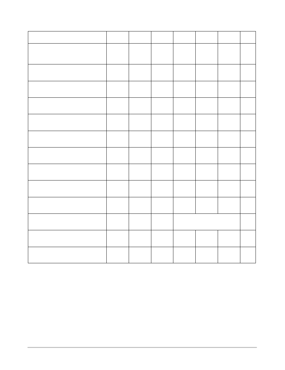
SWITCHING CHARACTERISTICS (Note 6.)
(C
L
= 50 pF, T
A
= 25_C)
Characteristic
Figure
Symbol
V
DD
Min
Typ
(Note 7.)
Max
Unit
Output Rise and Fall Time
t
TLH
, t
THL
= (1.5 ns/pF) C
L
+ 25 ns
t
TLH
, t
THL
= (0.75 ns/pF) C
L
+ 12.5 ns
t
TLH
, t
THL
= (0.55 ns/pF) C
L
+ 9.5 ns
2a
t
TLH
,
t
THL
5.0
10
15
—
—
—
100
50
40
200
100
80
ns
Clock to BCD Out
2a
t
PLH
,
t
PHL
5.0
10
15
—
—
—
900
500
200
1800
1000
400
ns
Clock to Overflow
2a
t
PHL
5.0
10
15
—
—
—
600
400
200
1200
800
400
ns
Reset to BCD Out
2b
t
PHL
5.0
10
15
—
—
—
900
500
300
1800
1000
600
ns
Clock to Latch Enable Setup Time
Master Reset to Latch Enable Setup Time
2b
t
su
5.0
10
15
600
400
200
300
200
100
—
—
—
ns
Removal Time
Latch Enable to Clock
2b
t
rem
5.0
10
15
– 80
– 10
0
– 200
– 70
– 50
—
—
—
ns
Clock Pulse Width
2a
t
WH(cl)
5.0
10
15
550
200
150
275
100
75
—
—
—
ns
Reset Pulse Width
2b
t
WH(R)
5.0
10
15
1200
600
450
600
300
225
—
—
—
ns
Reset Removal Time
—
t
rem
5.0
10
15
– 80
0
20
– 180
– 50
– 30
—
—
—
ns
Input Clock Frequency
2a
f
cl
5.0
10
15
—
—
—
1.5
5.0
7.0
0.9
2.5
3.5
MHz
Input Clock Rise Time
2b
t
TLH
5.0
10
15
No
Limit
ns
Disable, MR, Latch Enable
Rise and Fall Times
—
t
TLH
,
t
THL
5.0
10
15
—
—
—
—
—
—
15
5.0
4.0
μs
Scan Oscillator Frequency
(C1 measured in μF)
1
f
osc
5.0
10
15
—
—
—
1.5/C1
4.2/C1
7.0/C1
—
—
—
Hz
6. The formulas given are for the typical characteristics only at 25_C.
7. Data labelled “Typ” is not to be used for design purposes but is intended as an indication of the IC’s potential performance.
MC14553B
http://onsemi.com
5
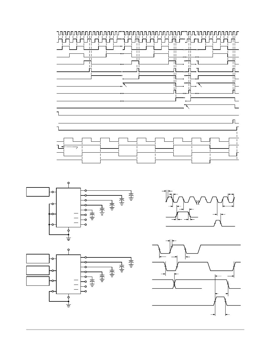
Figure 2. 3−Digit Counter Timing Diagram (Reference Figure 4)
1000
999
998
997
996
995
994
993
992
991
990
901
900
899
101
100
99
98
97
96
95
94
93
92
91
90
89
88
87
86
17
16
15
14
13
12
11
10
9
8
7
6
5
4
3
2
1
UNITS CLOCK
UNITS Q0
UNITS Q1
UNITS Q2
UNITS Q3
TENS CLOCK
TENS Q0
TENS Q3
HUNDREDS
CLOCK
HUNDREDS Q0
HUNDREDS Q3
DISABLE
OVERFLOW
MASTER
RESET
SCAN
OSCILLATOR
DIGIT SELECT 1
DIGIT SELECT 2
DIGIT SELECT 3
UP AT 80
UP AT 980
UP AT 800
(DISABLES CLOCK WHEN HIGH)
UNITS
TENS
HUNDREDS
PULSE
GENERATOR
(a)
16
V
DD
Q3
Q2
Q1
Q0
O.F.
DS1
DS2
DS3
8
V
SS
C
LE
DIS
MR
C
L
C
L
C
L
C
L
C
L
GENERATOR
1
(b)
V
DD
Q3
Q2
Q1
Q0
O.F.
DS1
DS2
DS3
V
SS
C
LE
MR
DIS
C
L
C
L
C
L
C
L
C
L
GENERATOR
2
GENERATOR
3
20 ns
20 ns
90%
10%
t
PLH
t
PHL
50%
50%
t
THL
t
TLH
10%
90%
50%
1/f
cl
t
WL(cl)
999
1000
t
TLH
50%
OVERFLOW
BCD OUT
CLOCK
90%
10%
t
rem
t
PHL
, t
PLH
50%
50%
50%
t
WH(R)
t
su
t
PHL
MASTER RESET
BCD OUT
LATCH
ENABLE
CLOCK
Figure 3. Switching Time Test Circuits and Waveforms
t
su
t
PHL
MC14553B
http://onsemi.com
6
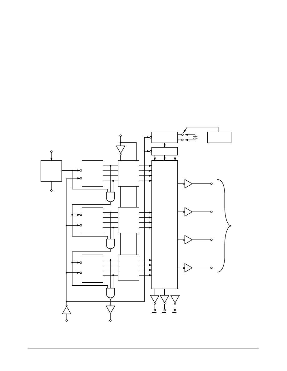
OPERATING CHARACTERISTICS
The MC14553B three−digit counter, shown in Figure 4,
consists of three negative edge−triggered BCD counters
which are cascaded in a synchronous fashion. A quad latch
at the output of each of the three BCD counters permits
storage of any given count. The three sets of BCD outputs
(active high), after going through the latches, are time
division multiplexed, providing one BCD number or digit at
a time. Digit select outputs (active low) are provided for
display control. All outputs are TTL compatible.
An on−chip oscillator provides the low frequency
scanning clock which drives the multiplexer output selector.
The frequency of the oscillator can be controlled externally
by a capacitor between pins 3 and 4, or it can be overridden
and driven with an external clock at pin 4. Multiple devices
can be cascaded using the overflow output, which provides
one pulse for every 1000 counts.
The Master Reset input, when taken high, initializes the
three BCD counters and the multiplexer scanning circuit.
While Master Reset is high the digit scanner is set to digit
one; but all three digit select outputs are disabled to prolong
display life, and the scan oscillator is inhibited. The Disable
input, when high, prevents the input clock from reaching the
counters, while still retaining the last count. A pulse shaping
circuit at the clock input permits the counters to continue
operating on input pulses with very slow rise times.
Information present in the counters when the latch input
goes high, will be stored in the latches and will be retained
while the latch input is high, independent of other inputs.
Information can be recovered from the latches after the
counters have been reset if Latch Enable remains high
during the entire reset cycle.
Figure 4. Expanded Block Diagram
PULSE
SHAPER
CLOCK
12
11
DISABLE
(ACTIVE
HIGH)
C
R
Q0
Q1
Q2
Q3
÷ 10
UNITS
C
R
Q0
Q1
Q2
Q3
÷ 10
TENS
C
R
Q0
Q1
Q2
Q3
÷ 10
HUNDREDS
10
LATCH ENABLE
QUAD
LATCH
QUAD
LATCH
QUAD
LATCH
R
R
SCAN
OSCILLATOR
SCANNER
PULSE
GENERATOR
C1
4
3
C1
A
C1
B
MULTIPLEXER
9
7
6
5
Q0
Q1
Q2
Q3
BCD
OUTPUTS
(ACTIVE
HIGH)
13
14
2
1
15
MR
(ACTIVE HIGH)
OVERFLOW
DS1
DS2
DS3
(LSD) DIGIT SELECT (MSD)
(ACTIVE LOW)
MC14553B
http://onsemi.com
7
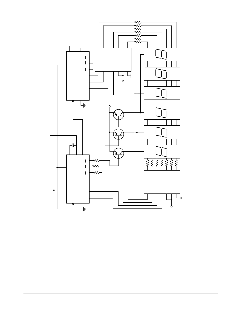
Figure 5. Six−Digit Display
V
DD
STROBE
RESET
CLOCK
INPUT
10
13
56
7
9
15
1
2
14
3
4
12
11
CLK
DIS
Q3
Q2
Q1
Q0
DS3
DS2
DS1
C1
A
C1
B
O.F
.
μ
0.001
F
5
3
2
4
6
1
7
A
B
C
D
Ph
LD
BI
a
b
c
d
e
f
g
9
10
11
12
13
15
14
MC14543B
LSD
V
DD
DISPLA
YS
ARE LOW CURRENT
LEDs
(I
peak
< 10 mA
PER SEGMENT)
MSD
V
DD
5
3
2
4
6
1
7
A
B
C
D
Ph
LD
BI
a
b
c
d
e
f
g
9
10
11
12
13
15
14
MC14543B
10
13
56
7
9
15
1
2
14
3
4
12
11
CLK
DIS
Q3
Q2
Q1
Q0
DS3
DS2
DS1
C1
A
C1
B
O.F
.
MC14553B
MC14553B
LE
MR
LE
MR
MC14553B
http://onsemi.com
8
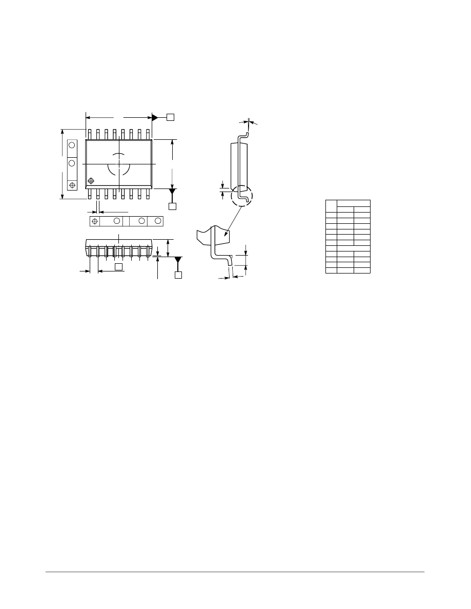
PACKAGE DIMENSIONS
PDIP−16
P SUFFIX
PLASTIC DIP PACKAGE
CASE 648−08
ISSUE R
NOTES:
1. DIMENSIONING AND TOLERANCING PER ANSI
Y14.5M, 1982.
2. CONTROLLING DIMENSION: INCH.
3. DIMENSION L TO CENTER OF LEADS WHEN
FORMED PARALLEL.
4. DIMENSION B DOES NOT INCLUDE MOLD FLASH.
5. ROUNDED CORNERS OPTIONAL.
−A−
B
F
C
S
H
G
D
J
L
M
16 PL
SEATING
1
8
9
16
K
PLANE
−T−
M
A
M
0.25 (0.010)
T
DIM
MIN
MAX
MIN
MAX
MILLIMETERS
INCHES
A
0.740
0.770
18.80
19.55
B
0.250
0.270
6.35
6.85
C
0.145
0.175
3.69
4.44
D
0.015
0.021
0.39
0.53
F
0.040
0.70
1.02
1.77
G
0.100 BSC
2.54 BSC
H
0.050 BSC
1.27 BSC
J
0.008
0.015
0.21
0.38
K
0.110
0.130
2.80
3.30
L
0.295
0.305
7.50
7.74
M
0
10
0
10
S
0.020
0.040
0.51
1.01
_
_
_
_
MC14553B
http://onsemi.com
9
PACKAGE DIMENSIONS
SOIC−16
DW SUFFIX
PLASTIC SOIC PACKAGE
CASE 751G−03
ISSUE B
D
14X
B
16X
SEATING
PLANE
S
A
M
0.25
B
S
T
16
9
8
1
h
X 45
_
M
B
M
0.25
H
8X
E
B
A
e
T
A1
A
L
C
q
NOTES:
1. DIMENSIONS ARE IN MILLIMETERS.
2. INTERPRET DIMENSIONS AND TOLERANCES
PER ASME Y14.5M, 1994.
3. DIMENSIONS D AND E DO NOT INLCUDE MOLD
PROTRUSION.
4. MAXIMUM MOLD PROTRUSION 0.15 PER SIDE.
5. DIMENSION B DOES NOT INCLUDE DAMBAR
PROTRUSION. ALLOWABLE DAMBAR
PROTRUSION SHALL BE 0.13 TOTAL IN EXCESS
OF THE B DIMENSION AT MAXIMUM MATERIAL
CONDITION.
DIM
MIN
MAX
MILLIMETERS
A
2.35
2.65
A1
0.10
0.25
B
0.35
0.49
C
0.23
0.32
D
10.15
10.45
E
7.40
7.60
e
1.27 BSC
H
10.05
10.55
h
0.25
0.75
L
0.50
0.90
q
0
7
_
_

MC14553B
http://onsemi.com
10
Notes

MC14553B
http://onsemi.com
11
Notes
ON Semiconductor and are registered trademarks of Semiconductor Components Industries, LLC (SCILLC). SCILLC reserves the right to make changes without further notice
to any products herein. SCILLC makes no warranty, representation or guarantee regarding the suitability of its products for any particular purpose, nor does SCILLC assume any liability
arising out of the application or use of any product or circuit, and specifically disclaims any and all liability, including without limitation special, consequential or incidental damages.
“Typical” parameters which may be provided in SCILLC data sheets and/or specifications can and do vary in different applications and actual performance may vary over time. All
operating parameters, including “Typicals” must be validated for each customer application by customer’s technical experts. SCILLC does not convey any license under its patent rights
nor the rights of others. SCILLC products are not designed, intended, or authorized for use as components in systems intended for surgical implant into the body, or other applications
intended to support or sustain life, or for any other application in which the failure of the SCILLC product could create a situation where personal injury or death may occur. Should
Buyer purchase or use SCILLC products for any such unintended or unauthorized application, Buyer shall indemnify and hold SCILLC and its officers, employees, subsidiaries, affiliates,
and distributors harmless against all claims, costs, damages, and expenses, and reasonable attorney fees arising out of, directly or indirectly, any claim of personal injury or death
associated with such unintended or unauthorized use, even if such claim alleges that SCILLC was negligent regarding the design or manufacture of the part. SCILLC is an Equal
Opportunity/Affirmative Action Employer. This literature is subject to all applicable copyright laws and is not for resale in any manner.
PUBLICATION ORDERING INFORMATION
N. American Technical Support: 800−282−9855 Toll Free
USA/Canada
Japan: ON Semiconductor, Japan Customer Focus Center
2−9−1 Kamimeguro, Meguro−ku, Tokyo, Japan 153−0051
Phone: 81−3−5773−3850
MC14553B/D
LITERATURE FULFILLMENT:
Literature Distribution Center for ON Semiconductor
P.O. Box 61312, Phoenix, Arizona 85082−1312 USA
Phone: 480−829−7710 or 800−344−3860 Toll Free USA/Canada
Fax: 480−829−7709 or 800−344−3867 Toll Free USA/Canada
Email: orderlit@onsemi.com
ON Semiconductor Website: http://onsemi.com
Order Literature: http://www.onsemi.com/litorder
For additional information, please contact your
local Sales Representative.
Wyszukiwarka
Podobne podstrony:
Impact On OIC Countries id 2122 Nieznany
Abolicja podatkowa id 50334 Nieznany (2)
4 LIDER MENEDZER id 37733 Nieznany (2)
katechezy MB id 233498 Nieznany
metro sciaga id 296943 Nieznany
perf id 354744 Nieznany
interbase id 92028 Nieznany
Mbaku id 289860 Nieznany
Probiotyki antybiotyki id 66316 Nieznany
miedziowanie cz 2 id 113259 Nieznany
LTC1729 id 273494 Nieznany
D11B7AOver0400 id 130434 Nieznany
analiza ryzyka bio id 61320 Nieznany
pedagogika ogolna id 353595 Nieznany
Misc3 id 302777 Nieznany
cw med 5 id 122239 Nieznany
D20031152Lj id 130579 Nieznany
więcej podobnych podstron