1
Data
Sheet
GP2D12
Optoelectronic Device
FEATURES
• Analog output
• Effective Range: 10 to 80 cm
• LED pulse cycle duration: 32 ms
• Typical response time: 39 ms
• Typical start up delay: 44 ms
• Average current consumption: 33 mA
• Detection area diameter @ 80 cm: 6 cm
DESCRIPTION
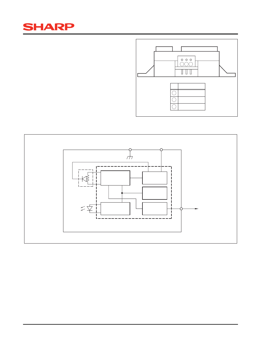
The GP2D12 is a distance measuring sensor with
integrated signal processing and analog voltage output.
Figure 1. Pinout
1
3
1
V
O
V
CC
GND
2
3
2
SIGNAL NAME
PIN
GP2D12-8
Figure 2. Block Diagram
GP2D12-4
SIGNAL
PROCESSING
CIRCUIT
PSD
LED
GND
V
CC
V
O
LED
DRIVE CIRCUIT
VOLTAGE
REGULATOR
OUTPUT
CIRCUIT
OSCILLATOR
CIRCUIT
DISTANCE MEASURING IC
GP2D12
2
Data
Sheet
ELECTRICAL SPECIFICATIONS
Absolute Maximum Ratings
Ta = 25°C, V
CC
= 5 VDC
Operating Supply Voltage
Electro-optical Characteristics
Ta = 25°C, V
CC
= 5 VDC
NOTES:
1. Measurements made with Kodak R-27 Gray Card, using the white side, (90% reflectivity).
2. L = Distance to reflective object.
PARAMETER
SYMBOL
RATING
UNIT
Supply Voltage
V
CC
-0.3 to +7.0
V
Output Terminal Voltage
V
O
-0.3 to (V
CC
+ 0.3)
V
Operating Temperature
Topr
-10 to +60
°C
Storage Temperature
Tstg
-40 to +70
°C
PARAMETER
SYMBOL
RATING
UNIT
Operating Supply Voltage
V
CC
4.5 to 5.5
V
PARAMETER
SYMBOL
CONDITIONS
MIN. TYP. MAX. UNIT NOTES
Measuring Distance Range
ΔL
10
-
80
cm
1, 2
Output Voltage
V
O
L = 80 cm
0.25
0.4
0.55
V
1, 2
Output Voltage Difference
ΔV
O
Output change at L change
(80 cm - 10 cm)
1.75
2.0
2.25
V
1, 2
Average Supply Current
I
CC
L = 80 cm
-
33
50
mA
1, 2
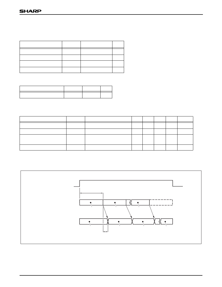
Figure 3. Timing Diagram
38.3 ms ±9.6 ms
5.0 ms MAX.
1st
MEASUREMENT
V
CC
(POWER SUPPLY)
V
O
(OUTPUT)
DISTANCE MEASURMENT
OPERATING
2nd
MEASUREMENT
nth
MEASUREMENT
UNSTABLE
OUTPUT
1st
OUTPUT
2nd
OUTPUT
nth
OUTPUT
GP2D12-5

GP2D12
3
Data
Sheet
RELIABILITY
The reliability of requirements of this device are
listed in Table 1.
NOTES:
1. Test conditions are according to Electro-optical Characteristics, shown on page 2.
2. At completion of the test, allow device to remain at nominal room temperature and humidity (non-condensing) for two hours.
3. Confidence level: 90%, Lot Tolerance Percent Defect (LTPD): 20% / 40%.
MANUFACTURER’S INSPECTION
Inspection Lot
Inspection shall be carried out per each delivery lot.
Inspection Method
A single sampling plan, normal inspection level II
based on ISO 2859 shall be adopted.
NOTE: *Any one of these that affects the Electro-optical Characteristics shall be considered a defect.
Table 1. Reliability
TEST ITEMS
TEST CONDITIONS
FAILURE
JUDGEMENT
CRITERIA
SAMPLES (n),
DEFECTIVE (C)
Temperature Cycling
One cycle -40°C (30 min.) to +70°C in 30
minutes, repeated 25 times
Initial × 0.8 > V
O
V
O
> Initial × 1.2
n = 11, C = 0
High Temperature and
High Humidity Storage
+40°C, 90% RH, 500h
n = 11, C = 0
High Temperature Storage
+70°C, 500h
n = 11, C = 0
Low Temperature Storage
-40°C, 500h
n = 11, C = 0
Operational Life
(High Temperature)
+60°C, V
CC
= 5 V, 500h
n = 11, C = 0
Mechanical Shock
100 m / s
2
, 6.0 ms
3 times / ±X, ±Y, ±Z direction
n = 6, C = 0
Variable Frequency Vibration
10-to-55-to-10 Hz i n 1 minute
Amplitude: 1.5 mm
2 h i n e a c h X, Y, Z direction
n = 6, C = 0
Table 2. Quality Level
DEFECT
INSPECTION ITEM and TEST METHOD
AQL (%)
Major Defect
Electro-optical characteristics defect
0.4
Minor Defect
Defect to appearance or dimensions (crack, split, chip, scratch, stain)*
1.0
GP2D12
4
Data
Sheet
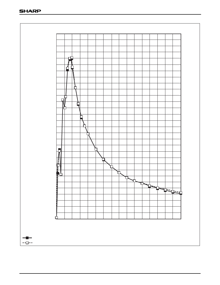
Figure 4. GP2D12 Example of Output/Distance Characteristics
3.0
2.8
2.6
2.4
2.2
2.0
1.8
1.6
1.4
1.2
1.0
0.8
0.6
0.4
0.2
0
10
20
30
40
50
60
70
80
DISTANCE TO REFLECTIVE OBJECT (cm)
ANALOG V
O
LT
A
G
E OUTPUT (V)
NOTES:
GP2D12-6
White paper (Reflectance ratio 90%)
Gray paper (Reflectance ratio 18%)
GP2D12
5
Data
Sheet
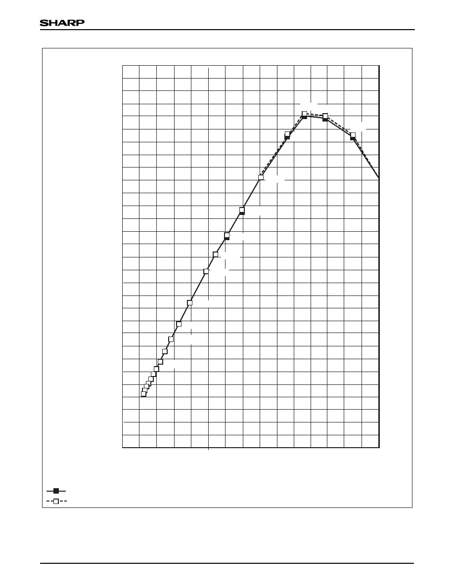
Figure 5. GP2D12 Example of Output Characteristics with Inverse Number of Distance
50 cm
0.00
0.2
0.4
0.6
0.8
1.0
1.2
1.4
1.6
1.8
2.0
2.2
2.4
2.6
2.8
3.0
0.02
0.04
0.06
0.08
0.10
0.12
0.14
40 cm
30 cm
28 cm
20 cm
18 cm
16 cm
14 cm
12 cm
10 cm
9 cm
8 cm
7 cm
INVERSE NUMBER OF DISTANCE 1/(L + 0.42) (1/cm)
ANALOG V
O
LT
A
G
E OUTPUT (V)
NOTES:
GP2D12-7
White paper (Reflectance ratio 90%)
Gray paper (Reflectance ratio 18%)
GP2D12
6
Data
Sheet
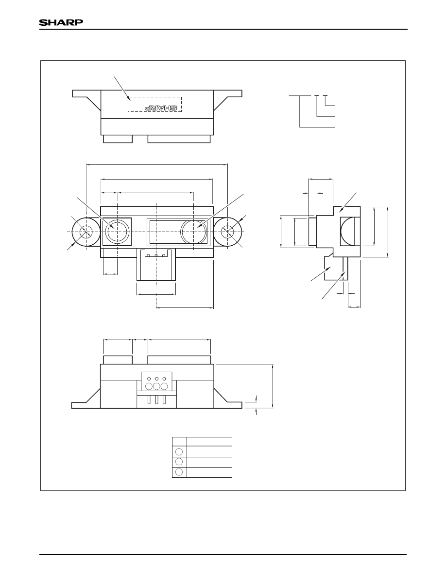
PACKAGE SPECIFICATIONS
φ3.2 HOLE
φ3.2 HOLE
STAMP
R3.75
LIGHT
DETECTOR
SIDE
R3.75
PCB
CONNECTOR
LIGHT
EMITTER
SIDE
STAMP EXAMPLE
GP2D12 5 3
Month (1 to 9, X, Y, Z)
Year (2005:5)
Model Name
10.1
3.75
7.2
8
.4
13.0
37.0
2.0
6.3
LENS
CASE
29.5
20 ±0.1 (Note 1)
4.5 (Note 1)
14.75
7.5
16.3
4.15
13.5
2-1.5
1.2
3.3
GP2D12 8
3
1
8
.9
+0.3
-0.3
1
3
1
V
O
Connector: J.S.T. Trading Company, LTD
S3B-PH
V
CC
GND
2
3
2
NOTES:
1. Dimensions shall reference lens center.
2. Unspecified tolerance shall be ±0.3 mm.
3. Scale: 2/1, dimensions are in mm.
GP2D12-3
SIGNAL NAME
PIN
CONNECTOR SIGNAL
GP2D12
7
Data
Sheet
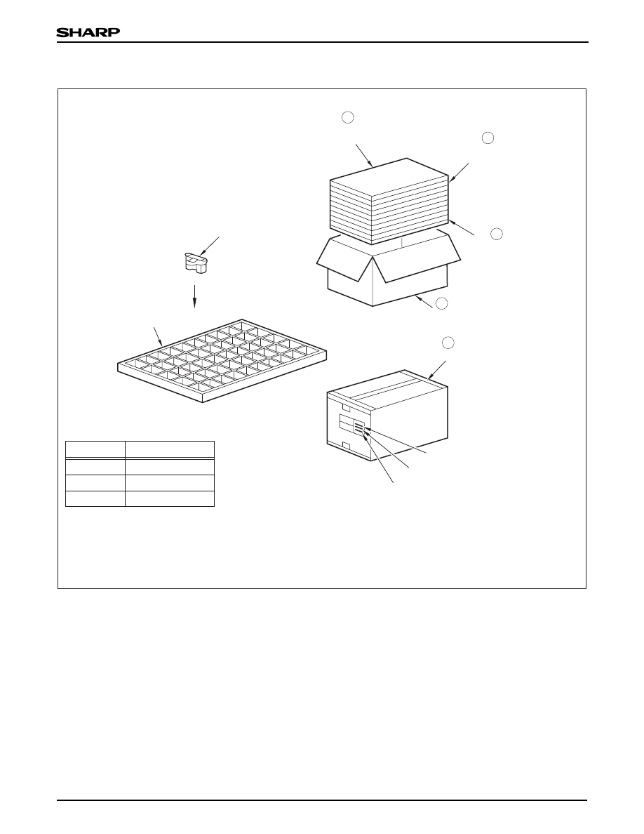
PACKING SPECIFICATION
TRAY
PACKING METHOD
1. Each tray holds 50 pieces. Packing methods are shown in (A).
2. Each box holds 10 trays. Pads are added to top and bottom, and between layers, as in (B).
top and bottom. Put pads between each tray (9 pads total) see above drawing (B).
3. The box is sealed with craft tape. (C) shows the location of the Model number, Quantity, and Inspection date.
4. Package weight: Approximately 4 kg.
MODEL NUMBER
CRAFT TAPE
PRODUCT TRAYS
(10-TRAY/CASE
)
PRODUCT
PAD (CORRUGATED
CARDBOARD)
(9 SHEETS/CASE
BETWEEN TRAYS)
PAD (CORRUGATED CARDBOARD
)
(2 SHEETS/CASE: TOP AND BOTTOM)
PACKING
CASE
QUANTITY
DATE
2
3
4
1
5
(A)
(B)
(C)
PART NAME
Packing case
Corrugated cardboard
Pad
Corrugated cardboard
Tray
Polystyrene
MATERIAL
GP2Y0A02YK-8
GP2D12
8
Data
Sheet
NOTES
• Keep the sensor lens clean. Dust, water, oil, and
other contaminants can deteriorate the characteris-
tics of this device. Applications should be designed
to eliminate sources of lens contamination.
• When using a protective cover over the emitter
and detector, ensure the cover efficiently transmits
light throughout the wavelength range of the LED
(
λ = 850 nm ± 70 nm). Both sides of the protective
cover should be highly polished. Use of a protective
cover may decrease the effective distance over
which the sensor operates. Ensure that any cover
does not negatively affect the operation over the
intended application range.
• Objects in proximity to the sensor may cause reflec-
tions that can affect the operation of the sensor.
• Sources of high ambient light (the sun or strong arti-
ficial light) may affect measurement. For best
results, the application should be designed to pre-
vent interference from direct sunlight or artificial light.
• Using the sensor with a mirror can induce measure-
ment errors. Often, changing the incident angle on
the mirror can correct this problem.
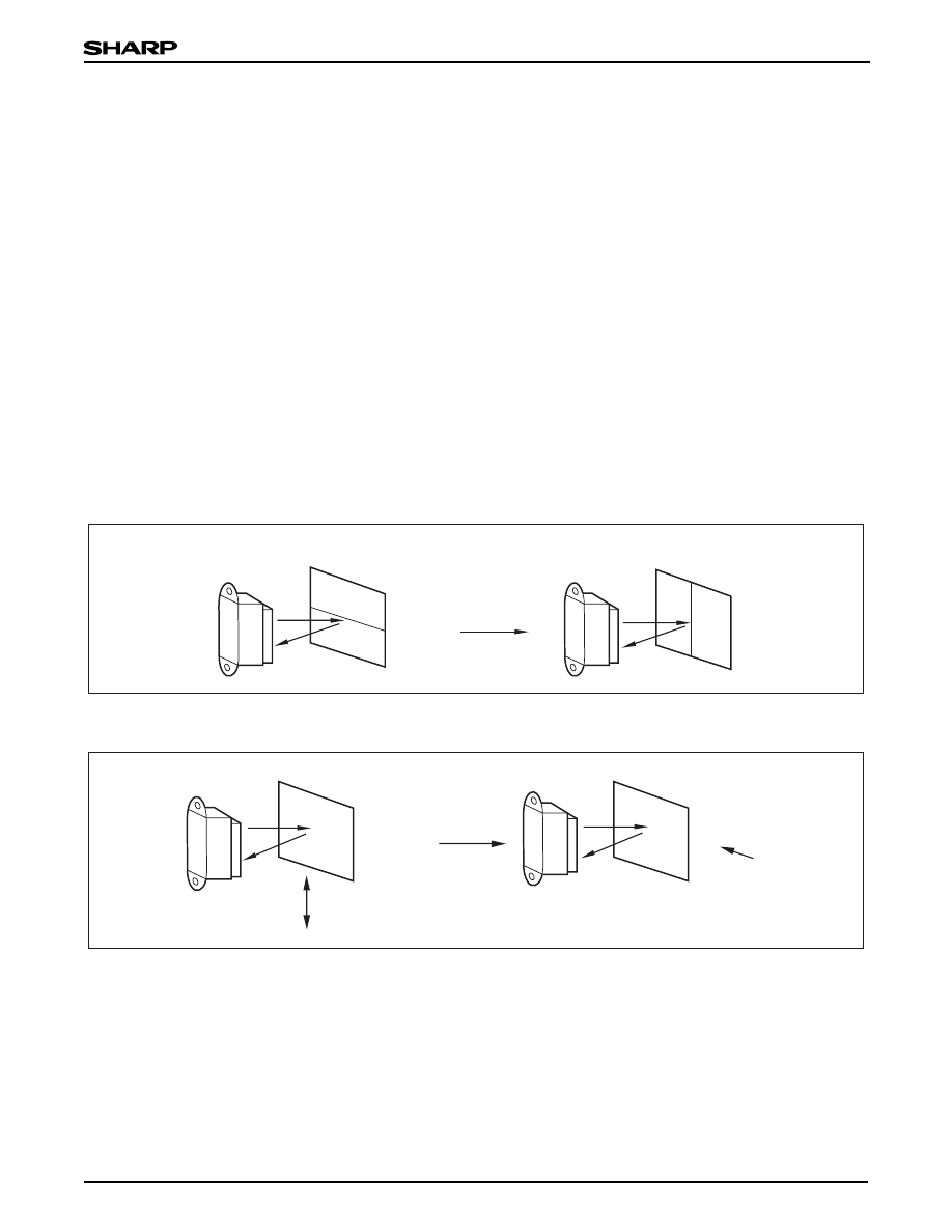
• If a prominent boundary line exists in the surface
being measured, it should be aligned vertically to
avoid measurement error. See Figure 6 for further
details.
• When measuring the distance to objects in motion,
align the sensor so that the motion is in the horizontal
direction instead of vertical. Figure 7 illustrates the
preferred alignment.
• A 10 µF (or larger) bypass capacitor between V
CC
and GND near the sensor is recommended.
• To clean the sensor, use a dry cloth. Use of any liq-
uid to clean the device may result in decreased sen-
sitivity or complete failure.
• Excessive mechanical stress can damage the
internal sensor or lens.
Figure 6. Proper Alignment to Surface Being Measured
Figure 7. Proper Alignment to Moving Surfaces
GP2D12-1
(AVOID IF POSSIBLE)
(PREFERRED)
GP2D12-2
(AVOID IF POSSIBLE)
(PREFERRED)
DIRECTION
OF MOVEMENT
DIRECTION
OF MOVEMENT

GP2D12
NOTICE
The circuit application examples in this publication are provided to explain representative applications of SHARP
devices and are not intended to guarantee any circuit design or license any intellectual property right. SHARP takes
no responsibility for any problems related to any intellectual property right of a third party resulting from the use of
SHARP devices.
SHARP reserves the right to make changes in the specifications, characteristics, data, materials, structures and
other contents described herein at any time without notice in order to improve design or reliability.
Contact SHARP in order to obtain the latest device specification sheets before using any SHARP device. Manu-
facturing locations are also subject to change without notice.
In the absence of confirmation by device specification sheets, SHARP takes no responsibility for any defects that
occur in equipment using any SHARP devices shown in catalogs, data books, etc.
The devices listed in this publication are designed for standard applications for use in general electronic equip-
ment. SHARP’s devices shall not be used for or in connection with equipment that requires an extremely high level
of reliability, such as military and aerospace applications, telecommunication equipment (trunk lines), nuclear power
control equipment and medical or other life support equipment (e.g. Scuba). SHARP takes no responsibility for dam-
age caused by improper use of device, which does not meet the conditions for use specified in the relevant specifi-
cation sheet.
If the SHARP devices listed in the publication fall within the scope of strategic products described in the Foreign
Exchange and Foreign Trade Law of Japan, it is necessary to obtain approval to export such SHARP devices.
This publication is the proprietary product of SHARP and is copyrighted, with all rights reserved. Under the copy-
right laws, no part of this publication may be reproduced or transmitted in any form or by any means, electronic or
mechanical for any purpose, in whole or in part, without the express written permission of SHARP. Express written
permission is also required before any use of this publication may be made by a third party.
Contact and consult with a SHARP representative if there are any questions about the contents of this publication.
9
Data Sheet

©2005 by SHARP Corporation
Reference Code SMA05006
SHARP CORPORATION
SALES & MARKETING GROUP
ELECTRONIC COMPONENTS & DEVICES
22-22 NAGAIKE-CHO, ABENO-KU, OSAKA 545-8522, JAPAN
PHONE: (81) 6-6621-1221
FAX: (81) 6117-725300, 6117-725301, 6117-725302
http://sharp-world.com/products/device
Specifications are subject to change without notice.
SHARP MICROELECTRONICS
OF THE AMERICAS
North American Head Office
5700 North West Pacific Rim Boulevard
Camas,Washington 98607 USA
PHONE: (1)360-834-2500
FAX: (1)360-834-8903
http://www.sharpsma.com
Western Area
1980 Zanker Road, San Jose, CA 95112
PHONE: (1)408-436-4900
FAX: (1)408-436-0924
5901 Bolsa Ave.
Huntington Beach, CA 92647-2053
PHONE: (1)714-903-4600
FAX: (1)714-903-0295
6390 Greenwich Drive, S uite 175
San Diego, CA 92122
PHONE: (1)858-597-0982
FAX: (1)858-597-8701
Central Area
85 W. Algonquin Road, Suite 280
Arlington Heights, IL 60005
PHONE: (1)847-258-2750
FAX: (1)847-439-2479
6303 Commerce Drive, Suite 175 Irving, TX 75063
PHONE: (1)972-582-1710
FAX: (1)972-580-7537
8911 Capitol of Texas Hwy. Suite 3130
Austin, TX 78759
PHONE: (1)512-349-7262
FAX: (1)512-349-7002
20333 State Hwy. 249, Suite 200 Houston, TX 77070
PHONE: (1)281-378-1520
FAX: (1)281-378-1521
W129 S 9647 Tony Lema Lane Muskego, WI 53150
PHONE: (1)414-529-9568
FAX: (1)414-529-9569
3001 West Big Beaver Road, Suite 722
Troy, ML 48084
PHONE: (1)248-458-1527
FAX: (1)248-458-6255
Eastern Area
1070 N. Kimbles Road, Yardley, PA 19067
PHONE: (1)215-321-5530
FAX: (1)215-321-5534
200 Wheeler Rd., Burlington, MA 01803
PHONE: (1)781-270-7979; (1)781-229-5100
FAX: (1)781-229-9117
8000 Regency Parkway, Suite 280 Cary, NC 27511
PHONE: (1)919-460-0695
FAX: (1)919-460-0795
2321 Sidney St. Pittsburgh, PA 15203
PHONE: (1)412-381-1191
FAX: (1)412-381-1192
4875 North Federal Highway, Third Floor
Ft. Lauderlade, FL 33318
PHONE: (1)954-267-8883
FAX: (1)954-267-0254
SHARP MICROELECTRONICS EUROPE
A division of Sharp Electronics (Europe) GmbH
Head Office
Sonninstrasse 3, 20097, Hamburg, Germany
PHONE: (49)180-5073507
FAX: (49)40-2376-2232
http://www.sharpsme.com/
Germany
SME München Office
Fuerstenriederstrasse 5, 80687 München, Germany
PHONE: (49)89-5468420
FAX: (49)89-54 684250
France
SME Paris Office
1 Rue Raoul Follereau Bussy Saint Georges
77608 Marne la Vallee Cedex 3
PHONE: (33)1 6476 22 22
FAX: (33)1 6476 22 23
Italy
SME Milano Office
Centro Direzionale Colleoni
Palazzo Taurus Ingresso 2
20041 Agrate Brianza, Milano, Italy
PHONE: (390)39-68 99 946
FAX: (390)39-68 99 948
U.K .
SME London Office
Centennial Court, Easthampstead Road,
Bracknell, Berkshire R G12 1YQ, United Kingdom
PHONE: (44)1344-86 99 22
FAX: (44)1344-36 09 03
Ireland
SME Dublin Office
First Floor, Block 1, St. Johns Court, Santry,
Dublin 9, Ireland
PHONE: (353)1-842 87 05
FAX: (353)1-842 84 55
SHARP ELECTRONICS (SHANGHAI) CO., LTD.
Microelectronics Sales & Marketing Division
16F, King Tower, 28 Xin Jin Qiao Road,
Pudong DIST, Shanghai 201206 P.R . China
PHONE: (86)21-5854-7710/21-5834-6056
FAX: (86)21-5854-4340/21-5834-6057
Registered Address
No. 11, De Bao Road, Xin Development BLDG
46 Wai Gao Qiao Free Trade Zone, Shanghai
200131, P.R . China
Beijing Office
Room 1062, Beijing Jing An Center No. 8 East
Bei San Huan Road, Chao Yang DIST, Beijing
100028 P.R . China
PHONE: (86) 10-6466-7543/10-6466-6561
FAX: (86) 10-6468-8920
http://sharp-world.com/products/devicechina/
index.html
SHARP-ROXY (HONG KONG) LTD.
Device Sales Division, 17/F, Admiralty Centre,
Tower 1, 18 Harcourt Road, Hong Kong
PHONE: (852)28229311
FAX: (852)28660779
http://www.sharp.com.hk
Shenzhen Representative Office
Room 13B1, Tower C, Electronics Science &
Technology Building, Shen Nan Zhong Road,
Shenzhen, P.R . China
PHONE: (86)755-83273731
FAX: (86)755-83273735
SHARP ELECTRONIC COMPONENTS
(TAIWAN) CORPORATION
8F-A, No. 16, Sec. 4, Nanking E. R d., Taipei, Taiwan
PHONE: (886)2-2577-7341
FAX: (886)2-2577-7326/2-2577-7328
SHARP ELECTRONICS (SINGAPORE) PTE ., LTD.
396 Alexandra Road #07-00
BP Tower Singapore 119954
PHONE: (65) 62713566
FAX: (65) 62713855
http://www.sesl-sharp.com
SHARP MICROELECTRONICS
TECHNOLOGY (M) SDN BHD.
Suite E 408, 4th Floor, East Tower,
Wisma Consplant 1, No. 2 J ln. SS 16/4,
Subng Jaya, 47500, Selangor Darul Ehsan, Malaysia
PHONE: (60) 3-5637-8964
FAX: (60) 3-5638-4029
SHARP ELECTRONIC COMPONENTS
(KOREA) CORPORATION
RM 501 iLsin B/D. 541, Dohwa-dong,
Mapo-ku, Seoul, Korea, 121-701
PHONE: (82)2-711-5813 ~ 8
FAX: (82)2-711-5819
U.S.A.
EUROPE
ASIA
Countries and Areas
Distributed By
Wyszukiwarka
Podobne podstrony:
czujniki obr PL id 129030 Nieznany
czujniki 2 id 129008 Nieznany
Abolicja podatkowa id 50334 Nieznany (2)
4 LIDER MENEDZER id 37733 Nieznany (2)
katechezy MB id 233498 Nieznany
metro sciaga id 296943 Nieznany
perf id 354744 Nieznany
interbase id 92028 Nieznany
Mbaku id 289860 Nieznany
Probiotyki antybiotyki id 66316 Nieznany
miedziowanie cz 2 id 113259 Nieznany
LTC1729 id 273494 Nieznany
D11B7AOver0400 id 130434 Nieznany
analiza ryzyka bio id 61320 Nieznany
pedagogika ogolna id 353595 Nieznany
Misc3 id 302777 Nieznany
cw med 5 id 122239 Nieznany
więcej podobnych podstron