
Part Number System Change Notice
Effective from August 6, 2007, a more concise part numbering system is utilized by
Hynix with the intention of managing product line with more consistency.
Devices developed after August 2007 and their respective products will be Refer to
the following pages for more details. (www.hynix.com/pn_notice.jsp)
Part Number with prefix ‘HY’ -> Old Part Number Decoder Link
Part Number with prefix ‘H’ -> New Part Number Decoder Link
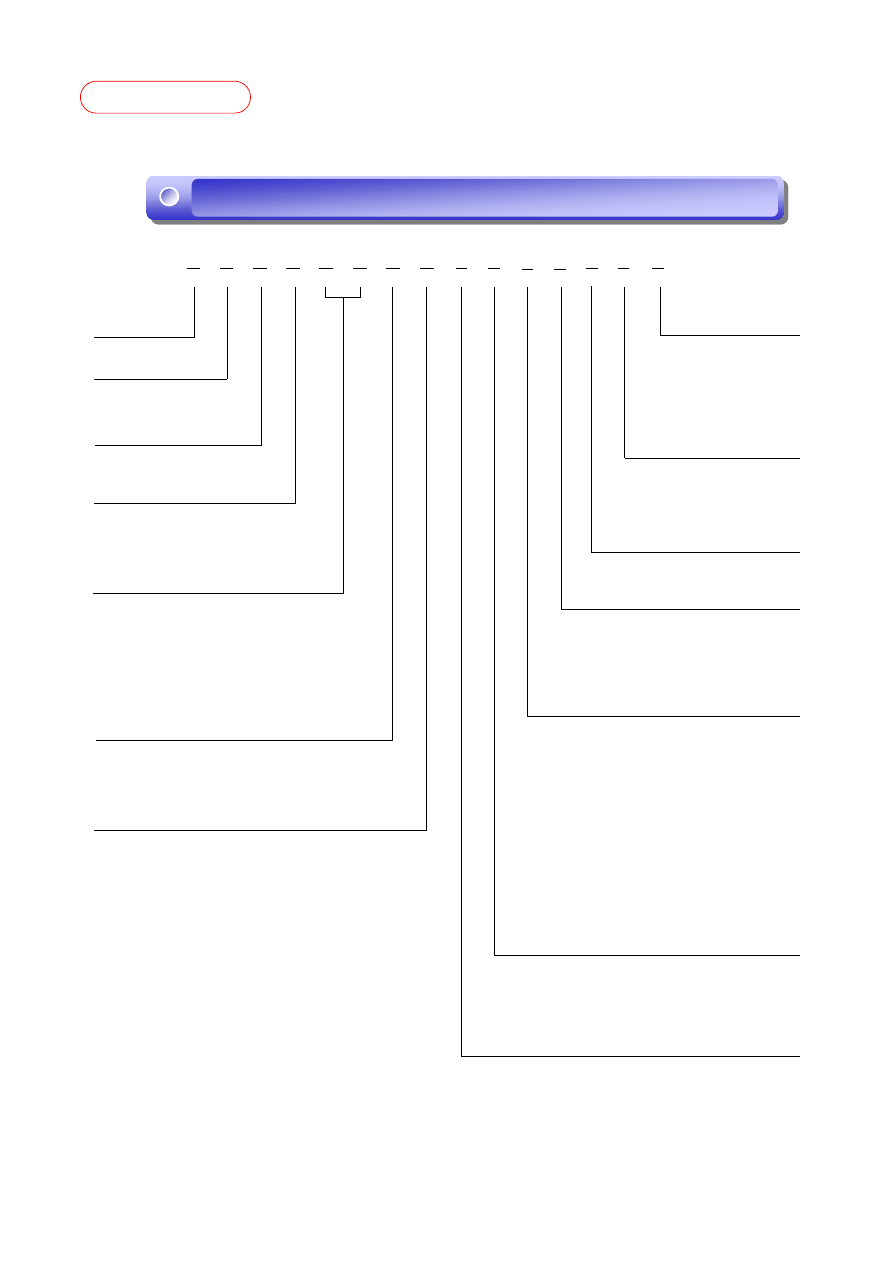
‘H’ Part Number Last Updated: Dec. 2007
H 2 7 X X X X X X X X X - X X
(
1) HYNIX
(2) PRODUCT FAMILY
(4) POWER SUPPLY(V
CC
)
(8) NAND CLASSIFICATION
(7) ORGANIZATION
(14) BAD BLOCK
(11) PACKAGE TYPE
2 : Flash
S
A
B
F
G
H
J
K
T
U
V
W
Y
: SLC + Single Die + Small Block
: SLC + Double Die + Small Block
: SLC + Quadruple Die + Small Block
: SLC + Single Die + Large Block
: SLC + Double Die + Large Block
: SLC + Quadruple Die + Large Block
: SLC + ODP + Large Block
: SLC + DSP + Large Block
: MLC + Single Die + Large Block
: MLC + Double Die + Large Block
: MLC + Quadruple Die + Large Block
: MLC + DSP + Large Block
: MLC + ODP + Large Block
C
E
M
I
B
S
P
: Included Bad Block
: 1~5 Bad Block Included
: All Good Block
T
V
S
N
W
D
X
Y
U
F
C
K
: TSOP1
: WSOP
: USOP
: LSOP1
: Wafer
: PGD2
: LGA
: VLGA
: ULGA
: FBGA
: PGD1 (chip)
: KGD
: 1st
: 2nd
: 3rd
: 4th
M
A
B
C
(5), (6) DENSITY
1
2
4
5
D
F
: 1 nCE & 1 R/nB; Sequential Row Read Enable
: 1 nCE & 1 R/nB; Sequential Row Read Disable
: 2 nCE & 2 R/nB; Sequential Row Read Enable
: 2 nCE & 2 R/nB; Sequential Row Read Disable
: Dual Interface; Sequential Row Read Disable
: 4 nCE & 4 R/nB ; Sequential Row Read Disable
(12) PACKAGE MATERIAL
A
P
L
R
: Wafer
: Lead Free
: Leaded
: Lead & Halogen Free
(1)
(4)
(2)
(3)
(5)
(7)
(6)
(9)
(15)
NAND Flash PART NUMBERING
NAND Flash PART NUMBERING
NAND Flash PART NUMBERING
NAND Flash PART NUMBERING
(8)
(10) (11) (12)
(14)
(13)
(3) PRODUCT MODE
7 : NAND Flash
U
L
S
: 2.7V~3.6V
: 2.7V
: 1.8V
64
25
1G
4G
AG
CG
: 64Mb
: 256Mb
: 1Gb
: 4Gb
: 16Gb
: 64Gb
12
51
2G
8G
BG
DG
: 128Mb
: 512Mb
: 2Gb
: 8Gb
: 32Gb
: 128Gb
8
6
: x8
: x16
(10) DIE GENERATION
(9) FUNCTION MODE
: Commercial (0℃~70℃)
: Extended (-25℃~85℃)
: Mobile (-30℃~85℃)
: Industrial (-40℃~85℃)
(13) -
d
“ - ”
(15) OPERATION
TEMPERATURE
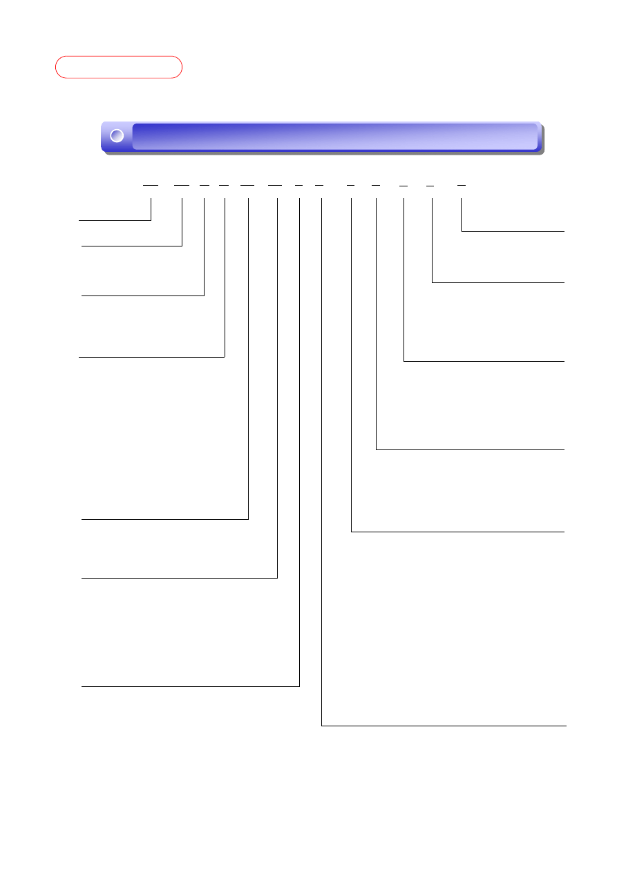
‘HY’ Part Number Last Updated: Dec. 2007
HY XX X X XX XX X X - X (X) (X) (X) (X)
(
1) HYNIX MEMORY
(2) COMPONENT GROUP
(3) POWER SUPPLY(V
CC
)
(4) CLASSIFICATION
(5) BIT ORGANIZATION
(11) OPERATING TEMPERATURE
(12) BAD BLOCK
(9) PACKAGE TYPE
(8) VERSION
: 2.7V~3.6V
: 2.7V
: 1.8V
27
: NAND Flash
U
L
S
S
A
B
F
G
H
K
T
U
V
W
: SLC + Single Die + S/B
: SLC + Double Die + S/B
: SLC + Quadruple Die + S/B
: SLC + Single Die + L/B
: SLC + Double Die + L/B
: SLC + Quadruple Die + L/B
: SLC + DSP + L/B
: MLC + Single Die + L/B
: MLC + Double Die + L/B
: MLC + Quadruple Die + L/B
: MLC + DSP + L/B
08
16
32
: x8
: x16
: x32
Blank
C
E
M
I
: Wafer, Chip
: 0℃~70℃
: -25℃~85℃
: -30℃~85℃
: -40℃~85℃
Blank
B
S
P
: Wafer
: Included Bad Block
: 1~5 Bad Block
: All Good Block
T
V
S
E
F
B
G
H
U
M
W
C
K
D
: TSOP1
: WSOP
: USOP
: WELP
: FBGA(63ball)
: FBGA(107ball)
: FBGA(149ball)
: TBGA
: ULGA
: VLGA
: Wafer
: Chip
: KGD
: PGD2
: 1st Gen.
: 2nd Gen.
: 3rd Gen.
: 4th Gen.
: Down Density(1st)
: Down Density(2nd)
M
A
B
C
1
2
(6) DENSITY
64
56
1G
4G
AG
CG
ZG
: 64Mb
: 256Mb
: 1Gb
: 4Gb
: 16Gb
: 64Gb
: 48Gb
(7) MODE
1
2
4
5
6
7
8
9
D
F
T
: 1 nCE & 1 R/nB; Sequential Row Read Enable
: 1 nCE & 1 R/nB; Sequential Row Read Disable
: 2 nCE & 2 R/nB; Sequential Row Read Enable
: 2 nCE & 2 R/nB; Sequential Row Read Disable
: 1 nCE & 1 R/nB; Sequential Row Read Enable & Auto Read Page 0
: 2 nCE & 2 R/nB; Sequential Row Read Enable & Auto Read Page 0
: 1 nCE & 1 R/nB; Sequential Row Read Disable & Auto Read Page 0
: 2 nCE & 2 R/nB; Sequential Row Read Disable & Auto Read Page 0
: Dual Interface; Sequential Row Read Disable
: 4 nCE & 4 R/nB ; Sequential Row Read Disable
: 3 nCE & 3 R/nB ; Sequential Row Read Disable
(13) OPTION(CUSTOMER)
Customer Initial
Option
(10) PACKAGE MATERIAL
Blank
P
H
R
: Normal, Wafer, Chip, KGD
: Lead Free
: Halogen Free
: Lead & Halogen Free
(1)
(3)
(2)
(3) (4)
(6)
(5)
(7)
(9)
(8)
(11)
(10)
(12)
(13)
NAND Flash PART NUMBERING
NAND Flash PART NUMBERING
NAND Flash PART NUMBERING
NAND Flash PART NUMBERING
28
12
2G
8G
BG
DG
: 128Mb
: 512Mb
: 2Gb
: 8Gb
: 32Gb
: 128Gb
Wyszukiwarka
Podobne podstrony:
Wykład VII hazard, realizacja na NAND i NOR
74F10 NAND 3 inp
badanie bramki NAND CMOS, -1-
7400 NAND
Badanie bramki NAND, BRAMKAnand, RADOM
Badanie bramki NAND, BRAMKAnand, RADOM
Wykład VII, hazard, realizacja na NAND i NOR
bramka nand
Objaśnienie zasady działania bramki NAND na podstawie struktury wewnętrznej wykonanej w technologii
Cw 21 Bramka NAND
ip lpec bramki AND,OR,NAND,NOR,NOT
Badanie bramki NAND Bramki
nand, TC
nand flash dwmm
Wykład VII hazard, realizacja na NAND i NOR
więcej podobnych podstron