LAB 3: Timer and Clock
Chung-Ta King
National Tsing Hua University
CS 4101 Introduction to Embedded Systems

Introduction
• In this lab, we will learn how to set up
and use
– The timer system of MSP430
– The clock system of MSP430
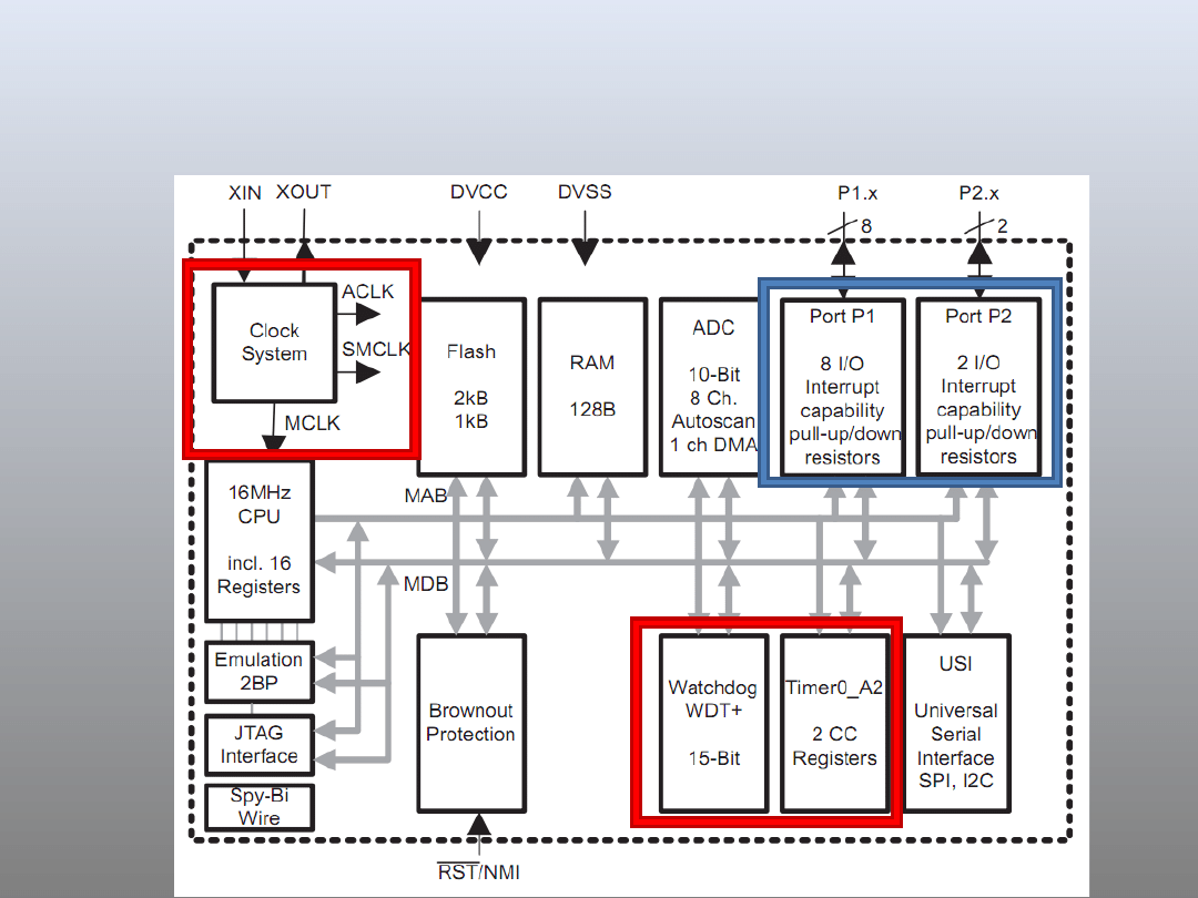
Inside MSP430
(MSP430G2x31)
IO
Clock
Syste
m
Timer
System
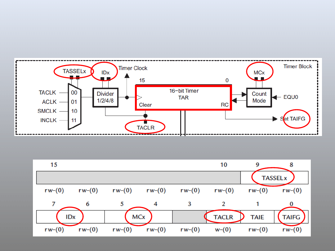
Inside Timer_A
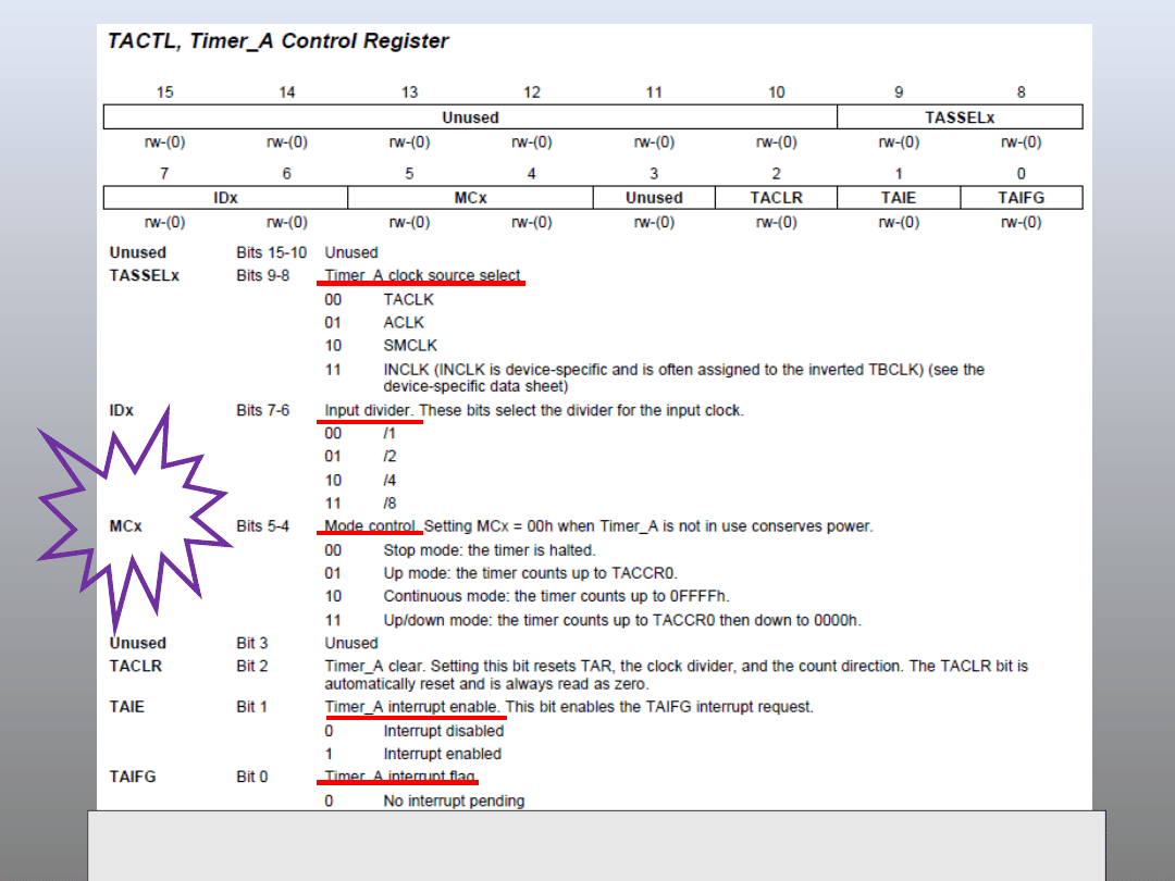
• Timer_A Control Register: TACTL
Typical Operations of
Timer_A
Continuously
count up/down
Is
time
up
yet?
TACCRx
Yes
If TAIE=1, setting
of TAIFG causes
an interrupt to the
CPU
TAIFG has to be
explicitly cleared
by the CPU
TACTL
TACTL = TASSEL_2 + MC_1;
// src from
SMCLK, up mode

Timer Mode
•MCx=00: Stop mode
–
The timer is halted
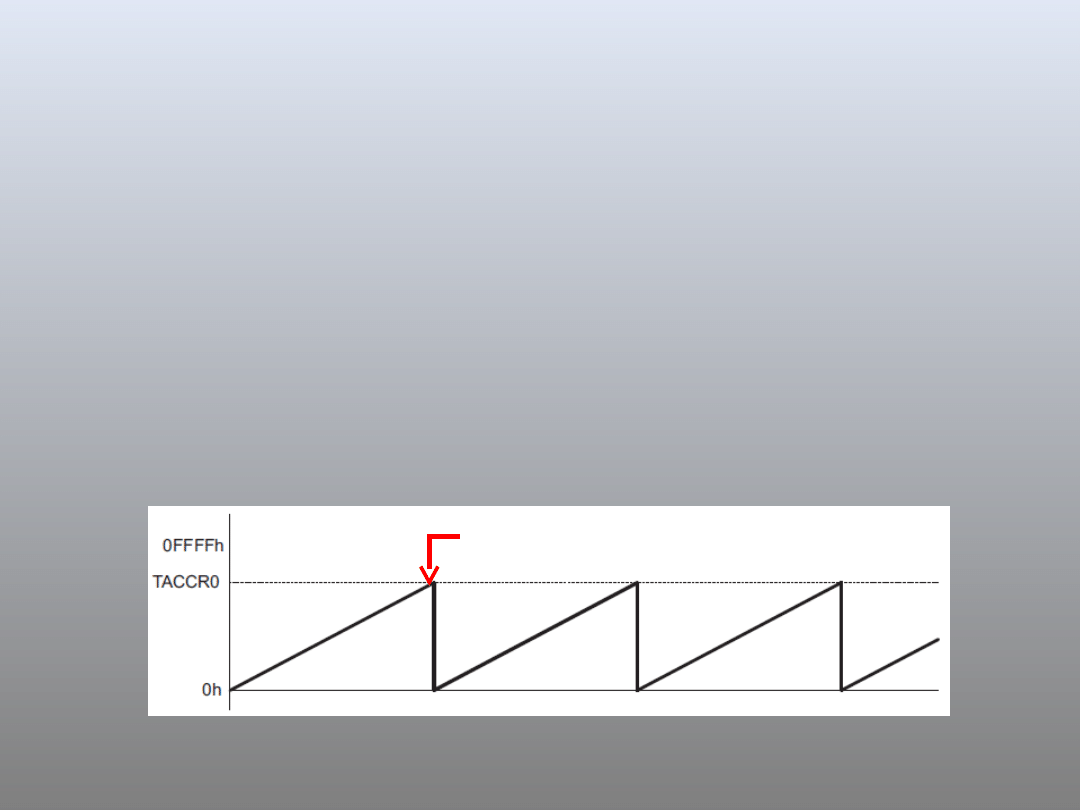
•MCx=01: Up mode
–
The timer repeatedly counts from 0 to TACCR0
•MCx=10: Continuous mode
–
The timer repeatedly counts from 0 to 0FFFFh
•MCx=11: Up/down mode
–
The timer repeatedly counts from 0 to TACCR0
and back down to 0
The up mode is used if the timer
period must be different from
0FFFFh counts.
1. Timer period 100 store 99 to TACCR0
2. When TACCR0 == 99, set TACCR0 CCIFG
interrupt flag
3. Reset timer to 0 and set TAIFG interrupt flag
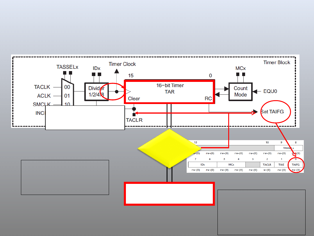
Up Mode
TAIFG is set, and
Timer_A interrupts
CPU
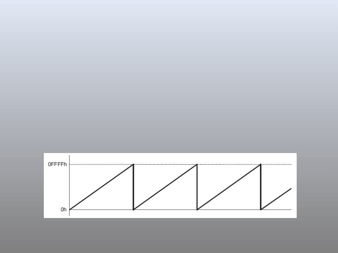
Continuous Mode
• In the continuous mode, the timer
repeatedly counts up to 0FFFFh and
restarts from zero
• The TAIFG interrupt flag is set when
the timer resets from 0FFFFh to zero
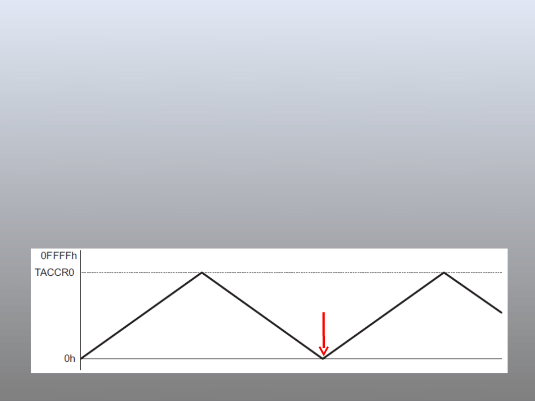
Up/down Mode
• The up/down mode is used if the
timer period must be different from
0FFFFh counts, and if a symmetrical
pulse generation is needed.
The period is twice the value
in TACCR0.
Timer
interrupts!
(TAIFG is set)
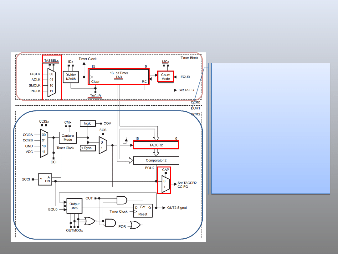
Timer_A Capture/Compare
Block
Timer Block
Capture/Compare Block
•May contain several
Capture/Compare
Blocks
•Each
Capture/Compare
Block is controlled by
a control register,
TACCTLx
•Inside each
Capture/Compare
Block, the
Capture/Compare
Register, TACCRx,
holds the count to
configure the timer
•May contain several
Capture/Compare
Blocks
•Each
Capture/Compare
Block is controlled by
a control register,
TACCTLx
•Inside each
Capture/Compare
Block, the
Capture/Compare
Register, TACCRx,
holds the count to
configure the timer

Modes of Capture/Compare
Block
• Compare mode:
– Compare the value of TAR with the value stored
in TACCRn and update an output when they
match
• Capture mode: used to record time events
– Records the “time” (value in TAR) at which the
input changes in TACCRx
– The input, usually CCIxA and CCIxB, can be
either external or internal from another
peripheral or software, depending on board
connections
TACCR0 = 24000;
// represent 2 sec with 12kHz clk src
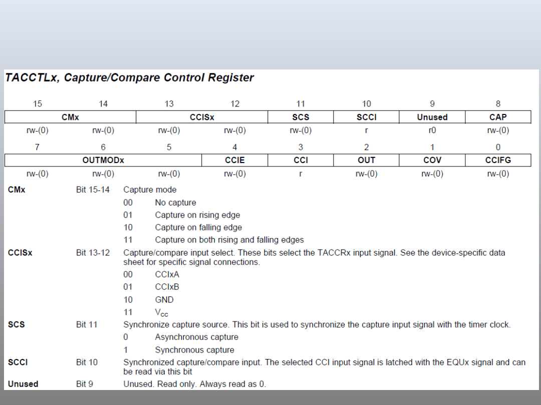
TACCTL
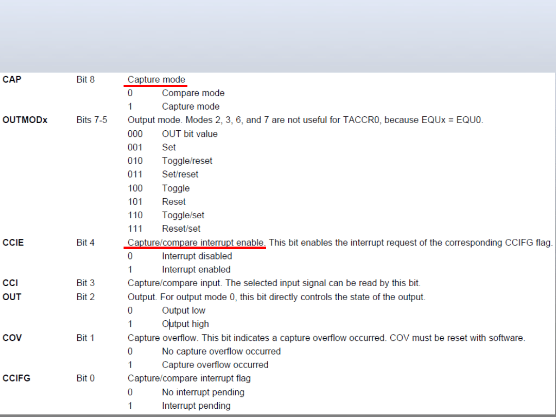
TACCTL cont’d
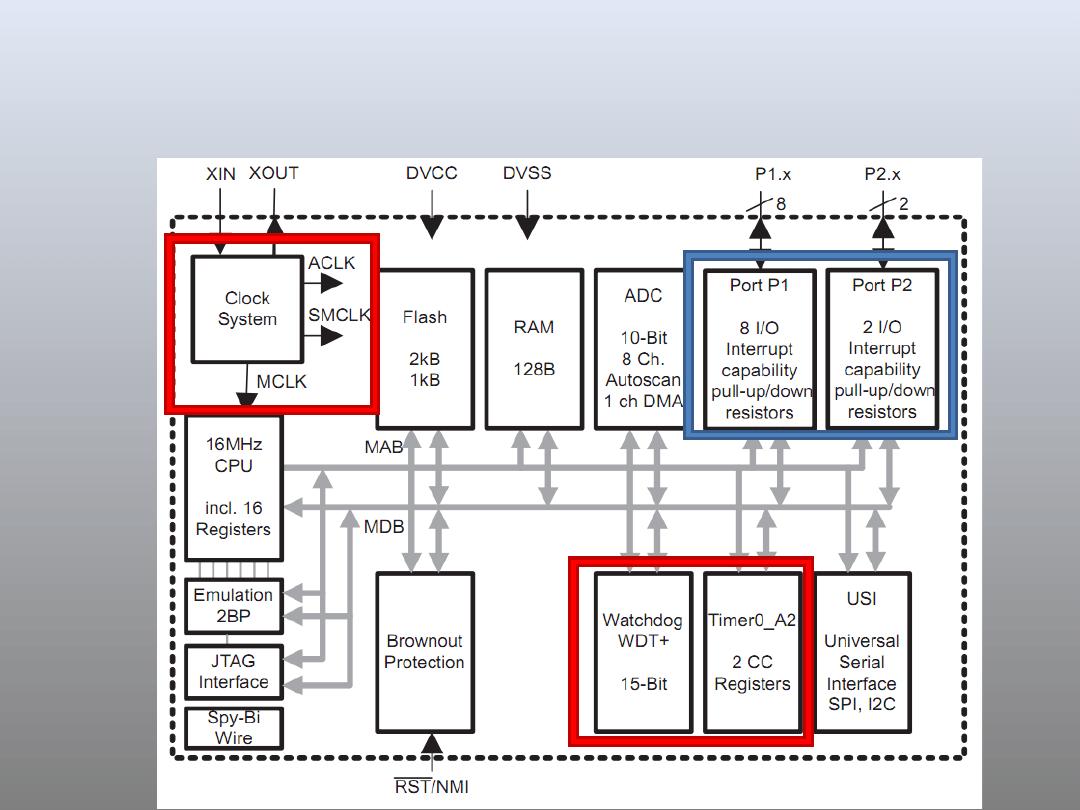
Inside MSP430
(MSP430G2x31)
IO
Clock
Syste
m
Timer
System

Theoretically, One Clock Is
Enough
• A clock is a square wave signal
whose edges trigger hardware
• A clock may be generated by various
sources of pulses, e.g. crystal
• But, systems have conflicting
requirements
– Low power, fast start/stop, accurate

Different Requirements for
Clocks
• Devices often in a low-power mode until
some event occurs, then must wake up and
handle event rapidly
– Clock must be stabilized quickly
• Devices also need to keep track of real
time: (1) can wake up periodically, or (2)
time-stamp external events
• Therefore, two kinds of clocks often needed:
– A fast clock to drive CPU, which can be started
and stopped rapidly but need not be accurate
– A slow clock that runs continuously to monitor
real time that uses little power and is accurate

Different Requirements for
Clocks
• Different clock sources also have different
characteristics
– Crystal: accurate and stable (w.r.t. temperature
or time); expensive, delicate, drawing large
current, external component, slow to start up or
stabilize
– Resistor and capacitor (RC): cheap, quick to
start, integrated within MCU and sleep with CPU;
poor accuracy and stability
– Ceramic resonator and MEMS clocks in between
Need multiple clocks

Clocks in MSP430
• MSP430 addresses the conflicting demands
for high performance, low power, precise
frequency by using 3 internal clocks, which
can be derived from up to 4 sources
– Master clock (MCLK):
for CPU & some
peripherals, normally driven by digitally
controlled oscillator (DCO) in megahertz range
– Subsystem master clock (SMCLK):
distributed
to peripherals, normally driven by DCO
– Auxiliary clock (ACLK):
distributed to
peripherals, normally for real-time clocking,
driven by a low-frequency crystal oscillator,
typically at 32 KHz

Clock Sources in MSP430
• Low- or high-frequency crystal oscillator, LFXT1:
–
External; used with a low- or high frequency crystal; an
external clock signal can also be used; connected to
MSP430 through XIN and XOUT pins
• High-frequency crystal oscillator, XT2:
–
External; similar to LFXT1 but at high frequencies
• Very low-power, low-frequency oscillator, VLO:
–
Internal at 12 KHz; alternative to LFXT1 when accuracy
of a crystal is not needed; may not available in all
devices
• Digitally controlled oscillator, DCO:
–
Internal; a highly controllable RC oscillator that starts
fast
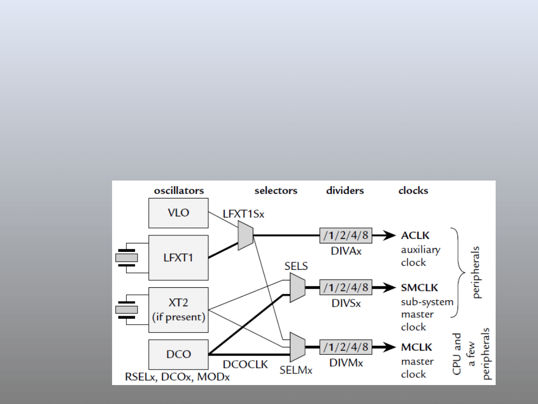
From Sources to Clocks
• Typical sources of clocks:
– MCLK, SMCLK: DCO (typically at 1.1
MHz)
– ACLK: LFXT 1 (typically at 32 KHz)
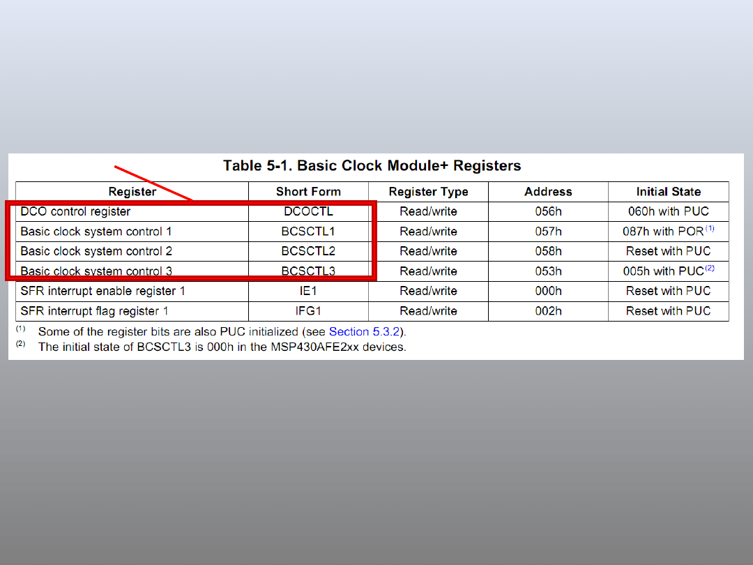
Control Registers for Clocks
• DCOCTL and BCSCTL1 combined define
the frequency of DCO, among other
settings
Control Registers for Clock
System
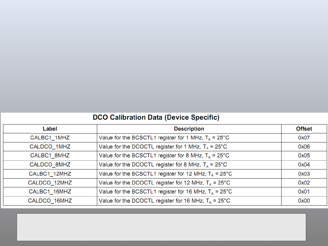
Simple Setting of DCO
• Can use Tag-Length-Value (TLV)
that are stored in the flash memory
to set DCOCTL and BCSCTL1 for DCO
frequency
BCSCTL1 = CALBC1_1MHZ;
// Set range
DCOCTL = CALDCO_1MHZ;
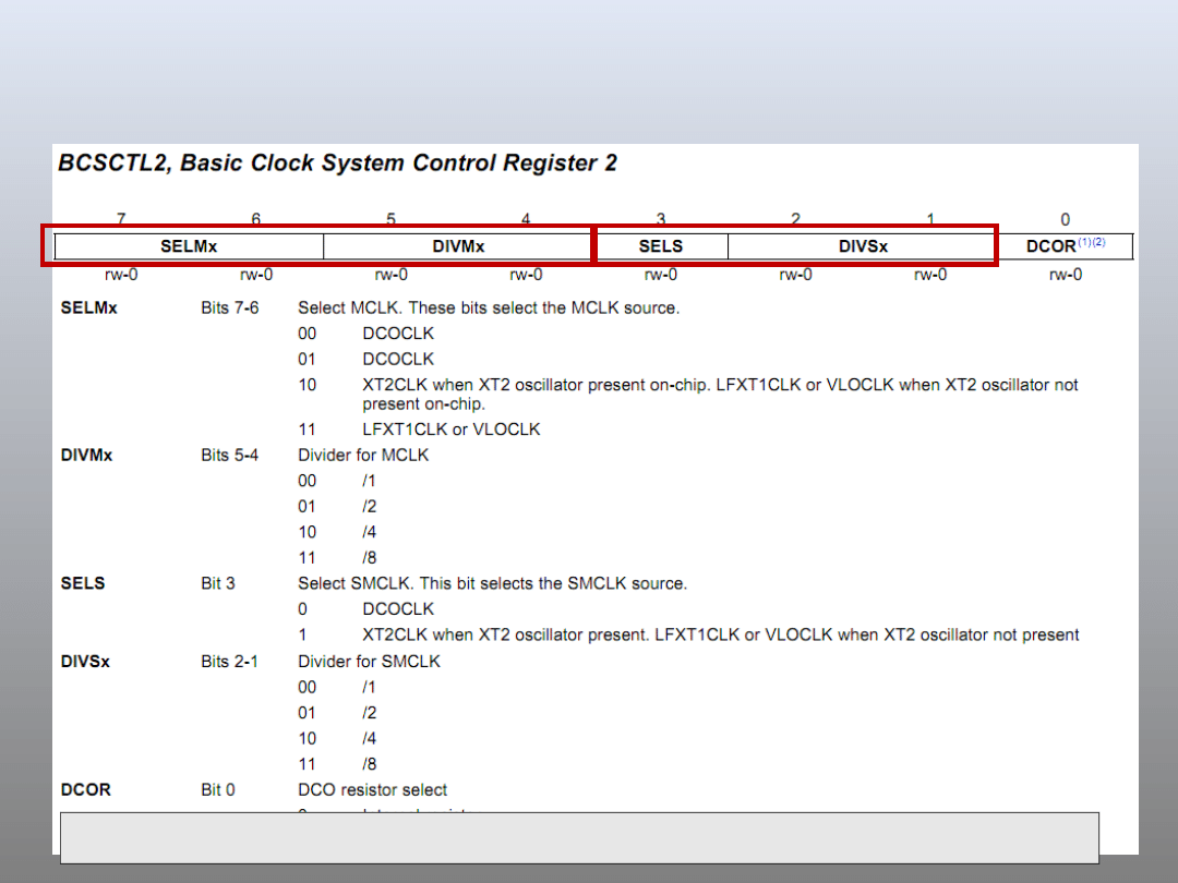
BCSCTL2
BCSCTL2 |= SELM_3 + DIVM_3;
// MCLK = VLO/8
MCL
K
SMCL
K
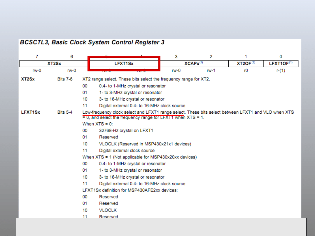
BCSCTL3
BCSCTL3 |= LFXT1S_2;
// Enable VLO as MCLK/ACLK
src
In
MSP430G223
1

Recall Sample Code for
Timer_A
#include <msp430g2553.h>
#define LED1 BIT0
void main (void) {
WDTCTL = WDTPW|WDTHOLD; // Stop watchdog timer
P1OUT = ~LED1;
P1DIR = LED1;
TACCR0 = 49999;
TACTL = MC_1|ID_3|TASSEL_2|TACLR; //Setup Timer_A
//up mode, divide clk by 8, use SMCLK, clr timer
for (;;) { // Loop forever
while (!(TACTL&TAIFG)) { // Wait time up
} // doing nothing
TACTL &= ~TAIFG; // Clear overflow flag
P1OUT ^= LED1; // Toggle LEDs
} // Back around infinite loop
}
• Flash red LED at 1 Hz if SMCLK at 800 KHz

Sample Code for Setting
Clocks
• Set DCO to 1MHz, enable crystal
#include <msp430g2231.h> (#include <msp430g2553.h> )
void main(void) {
WDTCTL = WDTPW + WDTHOLD;
// Stop watchdog timer
if (CALBC1_1MHZ ==0xFF || CALDCO_1MHZ == 0xFF)
while(1);
// If TLV erased, TRAP!
BCSCTL1 = CALBC1_1MHZ;
// Set range
DCOCTL = CALDCO_1MHZ;
P1DIR = 0x41;
// P1.0 & 6 outputs (red/green
LEDs)
P1OUT = 0x01;
// red LED on
BCSCTL3 |= LFXT1S_0;
// Enable 32768 crystal
IFG1 &= ~OFIFG;// Clear OSCFault flag
P1OUT = 0;
// red LED off
BCSCTL2 |= SELS_0 + DIVS_3;
// SMCLK = DCO/8
// infinite loop to flash LEDs
}

Basic Lab
• Flash green LED at 1 Hz by polling
Timer_A, which is driven by SMCLK
sourced by DCO running at 1 MHz.
–
Hint: Since TAR register is 16-bit (0~65535)
long, you should be careful of its overflow by
using clock source “Divider”.
• While keeping the green LED flashing at 1
Hz, pushing the button turns on the red
LED and releasing the button turns off the
red LED.
–
Hint: Your CPU has to poll two things
simultaneously, Timer_A and button

Bonus
• Whenever the button is pushed, turn
off the green LED and then turn on
the red LED for 2 sec. Afterwards,
return to normal flashing of the green
LED at 1 Hz.
• Use ACLK to drive Timer_A, sourced
from VLO (running at 12 KHz). The
green LED still needs to flash at 1 Hz.
Document Outline
- Slide 1
- Slide 2
- Slide 3
- Slide 4
- Slide 5
- Slide 6
- Slide 7
- Slide 8
- Slide 9
- Slide 10
- Slide 11
- Slide 12
- Slide 13
- Slide 14
- Slide 15
- Slide 16
- Slide 17
- Slide 18
- Slide 19
- Slide 20
- Slide 21
- Slide 22
- Slide 23
- Slide 24
- Slide 25
- Slide 26
- Slide 27
- Slide 28
- Slide 29
Wyszukiwarka
Podobne podstrony:
eksploracja lab03, Lista sprawozdaniowych bazy danych
LAB03
BO Lab03
506k timer ne555 regulator pwm
lab03
Lab03
Timer on off
TIMER
Programator czasowy (tajmer, timer) instrukcja PL
eksploracja-lab03 Ps 03
eksploracja-lab03 Opis bazy danych Document Understanding
Timer uniwersalny układ testowany UWC Plytka
Lab03 Switched LANs
Flipflop Timer
infa, Inf Lab03
Inf Lab03
PS lab03 mini lecture (DFT2)
Timer uniwersalny układ testowany UWC Opis
więcej podobnych podstron