SUP/SUB65P06-20
Vishay Siliconix
Document Number: 70289
S-05111—Rev. C, 10-Dec-01
www.vishay.com
2-1
P-Channel 60-V (D-S), 175
_
C MOSFET
PRODUCT SUMMARY
V
(BR)DSS
(V)
r
DS(on)
(
)
I
D
(A)
–60
0.020
–65
a
SUP65P06-20
SUB65P06-20
DRAIN connected to TAB
S
G
D
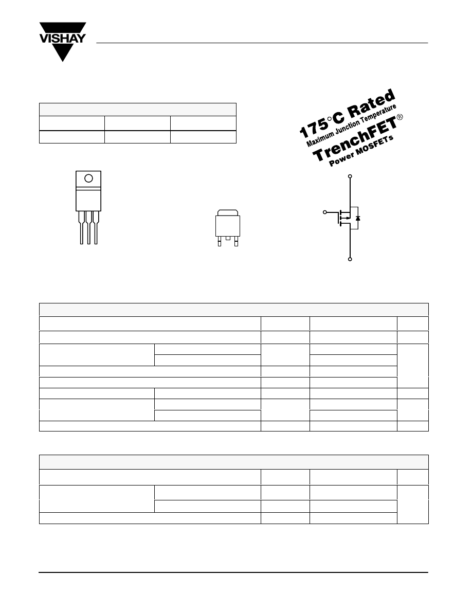
P-Channel MOSFET
TO-220AB
Top View
G D S
TO-263
S
G
Top View
D
ABSOLUTE MAXIMUM RATINGS (T
C
= 25_C UNLESS OTHERWISE NOTED)
Parameter
Symbol
Limit
Unit
Gate-Source Voltage
V
GS
"
20
V
Continuous Drain Current
T
C
= 25
_
C
–65
a
Continuous Drain Current
(T
J
= 175
_
C)
T
C
= 125
_
C
I
D
–39
Pulsed Drain Current
I
DM
–200
A
Avalanche Current
I
AR
–60
Repetitive Avalanche Energy
b
L = 0.1 mH
E
AR
180
mJ
T
C
= 25
_
C (TO-220AB and TO-263)
250
d
Power Dissipation
T
A
= 125
_
C (TO-263)
c
P
D
3.7
W
Operating Junction and Storage Temperature Range
T
J
, T
stg
–55 to 175
_
C
THERMAL RESISTANCE RATINGS
Parameter
Symbol
Limit
Unit
PCB Mount (TO-263)
c
R
thJA
40
Junction-to-Ambient
Free Air (TO-220AB)
R
thJA
62.5
_
C/W
Junction-to-Case
R
thJC
0.6
Notes:
a.
Package limited.
b.
Duty cycle
v
1%.
c.
When mounted on 1” square PCB (FR-4 material).
d.
See SOA curve for voltage derating.
For SPICE model information via the Worldwide Web: http://www.vishay.com/www/product/spice.htm
SUP/SUB65P06-20
Vishay Siliconix
www.vishay.com
S
FaxBack 408-970-5600
2-2
Document Number: 70289
S-05111—Rev. C, 10-Dec-01
SPECIFICATIONS (T
J
= 25_C UNLESS OTHERWISE NOTED)
Parameter
Symbol
Test Condition
Min
Typ
Max
Unit
Static
Drain-Source Breakdown Voltage
V
(BR)DSS
V
GS
= 0 V, I
D
= –250
A
–60
Gate Threshold Voltage
V
GS(th)
V
DS
= V
GS
, I
D
= –250
A
–2.0
–3.0
–4.0
V
Gate-Body Leakage
I
GSS
V
DS
= 0 V, V
GS
=
"
20 V
"
100
nA
V
DS
= –60 V, V
GS
= 0 V
–1
Zero Gate Voltage Drain Current
I
DSS
V
DS
= –60 V, V
GS
= 0 V, T
J
= 125
_
C
–50
DSS
V
DS
= –60 V, V
GS
= 0 V, T
J
= 175
_
C
–150
On-State Drain Current
a
I
D(on)
V
DS
= –5 V, V
GS
= –10 V
–120
A
V
GS
= –10 V, I
D
= –30 A
0.017
0.020
Drain-Source On-State Resistance
a
r
DS(on)
V
GS
= –10 V, I
D
= –30 A, T
J
= 125
_
C
0.033
DS(on)
V
GS
= –10 V, I
D
= –30 A, T
J
= 175
_
C
0.042
Forward Transconductance
a
g
fs
V
DS
= –15 V, I
D
= –30 A
25
S
Dynamic
b
Input Capacitance
C
iss
4500
Output Capacitance
C
oss
V
GS
= 0 V, V
DS
= –25 V, f = 1 MHz
870
pF
Reversen Transfer Capacitance
C
rss
350
Total Gate Charge
c
Q
g
85
120
Gate-Source Charge
c
Q
gs
V
DS
= –30 V,
V
GS
= –10 V, I
D
= –65 A
24
nC
Gate-Drain Charge
c
Q
gd
DS
GS
D
22
Turn-On Delay Time
c
t
d(on)
15
40
Rise Time
c
t
r
V
DD
= –30 V, R
L
= 0.47
40
80
Turn-Off Delay Time
c
t
d(off)
V
DD
= –30 V, R
L
= 0.47
I
D
]
–65 A, V
GEN
= –10 V, R
G
= 2.5
65
120
ns
Fall Time
c
t
f
D
GEN
G
30
60
Source-Drain Diode Ratings and Characteristics (T
C
= 25
_
C)
b
Continuous Current
I
s
–65
Pulsed Current
I
SM
–200
A
Forward Voltage
a
V
SD
I
F
= –65 A, V
GS
= 0 V
–1.1
–1.4
V
Reverse Recovery Time
t
rr
70
120
ns
Peak Reverse Recovery Current
I
RM(REC)
I
F
= –65 A, di/dt = 100 A/
s
7
9
A
Reverse Recovery Charge
Q
rr
F
0.245
0.54
C
Notes:
a.
Pulse test; pulse width
v
300
s, duty cycle
v
2%.
b.
Guaranteed by design, not subject to production testing
d.
Independent of operating temperature.
SUP/SUB65P06-20
Vishay Siliconix
Document Number: 70289
S-05111—Rev. C, 10-Dec-01
www.vishay.com
2-3
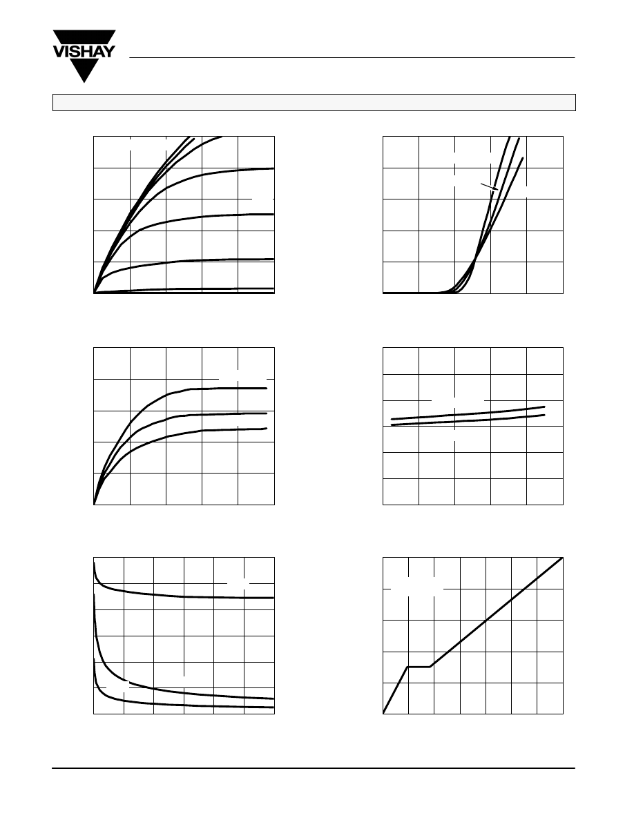
TYPICAL CHARACTERISTICS (25_C UNLESS NOTED)
0
4
8
12
16
20
0
25
50
75
100
125
150
175
0.000
0.005
0.010
0.015
0.020
0.025
0.030
0
20
40
60
80
100
0
1000
2000
3000
4000
5000
6000
0
10
20
30
40
50
60
0
20
40
60
80
100
0
20
40
60
80
100
0
40
80
120
160
200
0
2
4
6
8
10
0
40
80
120
160
200
0
2
4
6
8
10
Output Characteristics
Transfer Characteristics
Capacitance
Gate Charge
Transconductance
On-Resistance vs. Drain Current
V
DS
– Drain-to-Source Voltage (V)
–
Drain Current (A)
I
D
V
GS
– Gate-to-Source Voltage (V)
–
Drain Current (A)
I
D
–
Gate-to-Source V
oltage (V)
–
On-Resistance (
Q
g
– Total Gate Charge (nC)
I
D
– Drain Current (A)
V
DS
– Drain-to-Source Voltage (V)
C
–
Capacitance (pF)
r DS(on)
)
V
GS
V
GS
– Gate-to-Source Voltage (V)
–
T
ransconductance
(S)
g
fs
25
_
C
125
_
C
6 V
T
C
= –55
_
C
V
DS
= 30 V
I
D
= 65 A
V
GS
= 10, 9, 8 V
7 V
V
GS
= 10 V
V
GS
= 20 V
C
iss
C
oss
C
rss
T
C
= –55
_
C
25
_
C
125
_
C
5 V
4 V
SUP/SUB65P06-20
Vishay Siliconix
www.vishay.com
S
FaxBack 408-970-5600
2-4
Document Number: 70289
S-05111—Rev. C, 10-Dec-01
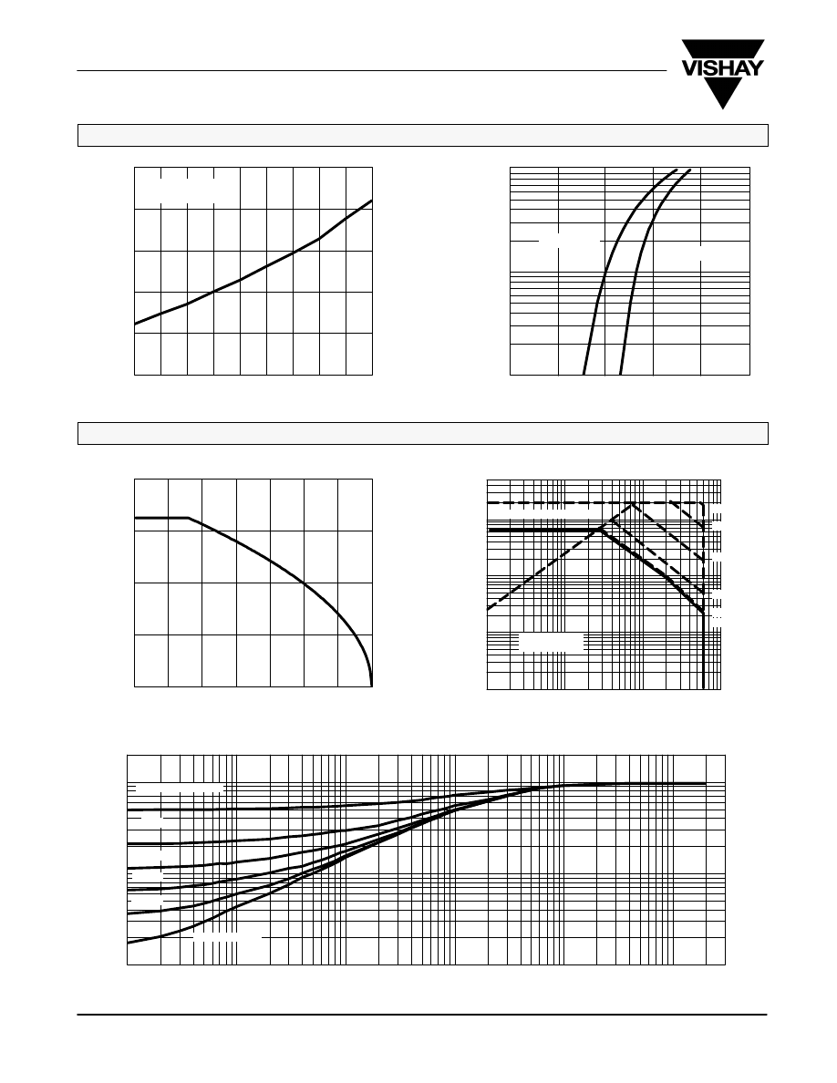
TYPICAL CHARACTERISTICS (25_C UNLESS NOTED)
0.0
0.5
1.0
1.5
2.0
2.5
–50
–25
0
25
50
75
100
125
150
175
On-Resistance vs. Junction Temperature
Source-Drain Diode Forward Voltage
(Normalized)
–
On-Resistance (
T
J
– Junction Temperature (
_
C)
V
SD
– Source-to-Drain Voltage (V)
r DS(on)
)
–
Source Current (A)
I
S
100
10
1
0.3
0.6
0.9
1.2
1.5
V
GS
= 10 V
I
D
= 30 A
T
J
= 25
_
C
T
J
= 150
_
C
0.3
THERMAL RATINGS
0
20
40
60
80
0
25
50
75
100
125
150
175
Normalized Thermal Transient Impedance, Junction-to-Case
Square Wave Pulse Duration (sec)
2
1
0.1
0.01
10
–5
10
–4
10
–3
10
–2
10
–1
1
Normalized Ef
fective
T
ransient
Thermal Impedance
3
Safe Operating Area
Maximum Avalanche and Drain Current
vs. Case Temperature
T
C
– Case Temperature (
_
C)
V
DS
– Drain-to-Source Voltage (V)
–
Drain Current (A)
ID
–
Drain Current (A)
ID
0.2
0.1
0.05
0.02
Single Pulse
Duty Cycle = 0.5
100
500
10
0.1
10
s
100
s
1 ms
10 ms
100 ms
dc
T
C
= 25
_
C
Single Pulse
Limited by r
DS(on)
0.1
1
10
100
1

Document Number: 91000
www.vishay.com
Revision: 18-Jul-08
1
Disclaimer
Legal Disclaimer Notice
Vishay
All product specifications and data are subject to change without notice.
Vishay Intertechnology, Inc., its affiliates, agents, and employees, and all persons acting on its or their behalf
(collectively, “Vishay”), disclaim any and all liability for any errors, inaccuracies or incompleteness contained herein
or in any other disclosure relating to any product.
Vishay disclaims any and all liability arising out of the use or application of any product described herein or of any
information provided herein to the maximum extent permitted by law. The product specifications do not expand or
otherwise modify Vishay’s terms and conditions of purchase, including but not limited to the warranty expressed
therein, which apply to these products.
No license, express or implied, by estoppel or otherwise, to any intellectual property rights is granted by this
document or by any conduct of Vishay.
The products shown herein are not designed for use in medical, life-saving, or life-sustaining applications unless
otherwise expressly indicated. Customers using or selling Vishay products not expressly indicated for use in such
applications do so entirely at their own risk and agree to fully indemnify Vishay for any damages arising or resulting
from such use or sale. Please contact authorized Vishay personnel to obtain written terms and conditions regarding
products designed for such applications.
Product names and markings noted herein may be trademarks of their respective owners.
Document Outline
- Datasheet
- Disclaimer
- Datasheet
- Disclaimer
Wyszukiwarka
Podobne podstrony:
Zawal serca 20 11 2011
20 Rysunkowa dokumentacja techniczna
Prezentacja 20 10
20 2id 21226 ppt
20 H16 POST TRANSFUSION COMPLICATIONS KD 1st part PL
20 Tydzień zwykły, 20 środa
3 Analiza firmy 2015 (Kopia powodująca konflikty (użytkownik Maciek Komputer) 2016 05 20)
Prezentacja 20
plik (20)
20
20 Księga Przypowieści Salomona
01 Top 20 ports
cw 20 Instrukcja
chojnicki 1999 20 problemy GP
20 12id 21221
24 gold & 20's
Podstawy Teorii Okretow Pytania nr 4 (20) id 368475
20 Stosowanie zasad projektowan Nieznany (2)
więcej podobnych podstron