2008-2013 Microchip Technology Inc.
DS00000734C-page 1
AN734
INTRODUCTION
Several of the Mid-Range Enhanced Core PIC16
microcontroller devices have a Master Synchronous
Serial Port (MSSP). The MSSP module can be used to
implement either I
2
C™ or SPI communications proto-
col. In this application note, the basics of the I
2
C slave
protocol will be covered. The reader should then have
a better understanding of the MSSP module and how it
is used for slave communication on an I
2
C bus. Code
examples will also be provided to assist the reader in
implementing the modules into their own designs.
For more information regarding the I
2
C bus
specification, or to learn more about the MSSP module,
please refer to the sources list in the
of this application note.
THE I
2
C BUS SPECIFICATION
The Inter-Integrated Circuit (I
2
C) bus is a widely used
industry standard developed by Philips
®
Inc. for the
transfer of data between integrated circuits, such as
serial EEPROMs or other microcontrollers. Devices
communicate in a master/slave environment in which
the master always initiates the communication, and the
slave device is controlled through addressing. An I
2
C
bus can have one or more master devices and one or
more slave devices. The master device is the device
that initiates a data transfer on the bus, and is
responsible for generating the serial clock used on the
bus. Any addressed device is then considered a slave.
The I
2
C protocol supports either 7-bit or 10-bit
Addressing modes. Data transfers are performed eight
bits at a time, starting with the MSb. Each device is
recognized by a unique address and can operate as
either a transmitter or receiver.
The physical interface of the bus consists of two
bidirectional open-drain lines, one line used for the
serial clock (SCL), and the other used for serial data
(SDA). Each line will require a pull-up resister to supply
voltage to the lines. Pulling the line to ground is consid-
ered a logical Low, while letting the line float is consid-
ered a logical High. When the bus is free, both SDA and
SCL are logical High. Data can be transferred at a rate
up to 100 kbits/s in the Standard mode, up to 400
kbits/s in Fast mode, up to 1 Mbits/s in Fast mode Plus,
or up to 3.4 Mbits/s in High-Speed mode. Data on the
SDA line must be stable during the high period of the
clock. Any changes on the SDA line can only occur
when the clock signal on the SCL line is low. One clock
pulse is generated for each transferred data bit.
The I
2
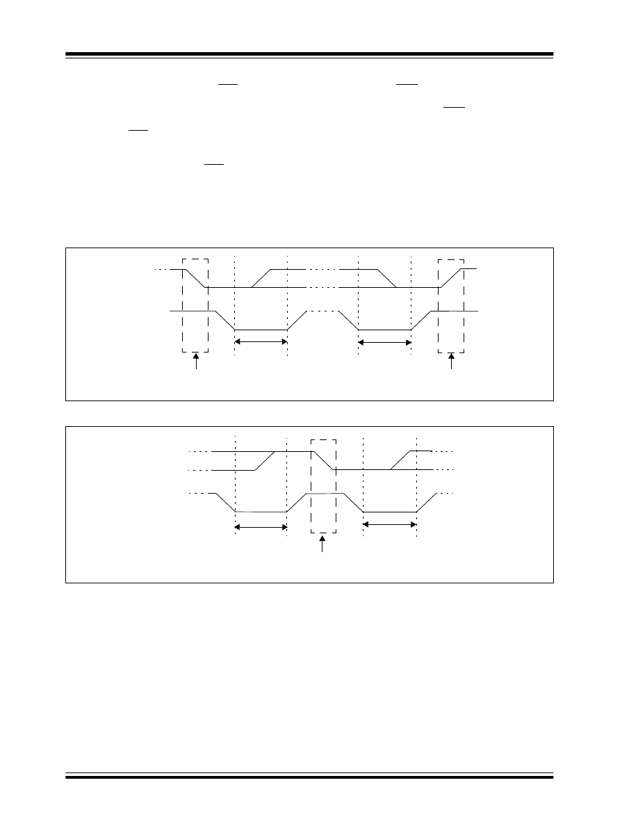
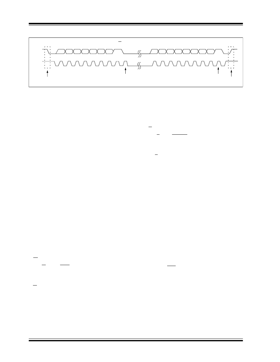
C specification defines a Start condition as a
transition of the SDA line from a high to a low state,
while the SCL line is high. A Start condition is always
generated by the master and signifies the transition of
the bus from an Idle to an Active state. The I
2
C specifi-
cation states that no bus collision can occur on a Start;
however, a bus collision can occur if the MSSP module
samples the SDA line low before asserting it low.
A Stop condition is a transition of the SDA line from
low-to-high state while the SCL line is high. At least one
SCL low time must appear before a Stop is valid.
Therefore, if the SDA line goes low, then high again,
while the SCL line stays high, only the Start condition is
detected.
A Restart, or Repeated Start, is valid any time that a
Stop would be valid. A master can issue a Restart if it
wishes to hold the bus after terminating the current
transfer. A Restart has the same effect on the slave that
a Start would, resetting all slave logic and preparing it
to clock in an address. The master may want to
address the same or another slave. This can be useful
for many I
2
C peripherals, such as nonvolatile EEPROM
memory, in which an I
2
C write operation and a read
operation are done in succession. In this case, the write
operation specifies the address to be read and the read
operation gets the byte of data. Since the master
device does not release the bus after the memory
address is written to the device, a Restart sequence is
performed to read the contents of the memory address.
In 10-bit Addressing Slave mode, a Restart is required
for the master to clock data out of the addressed slave.
Once a slave has been fully addressed, matching both
high and low address bytes, the master can issue a
Restart and send the high address byte with the R/W bit
set. The slave logic will then hold the clock and prepare
to clock out data. After a full match with R/W clear in
10-bit mode, a prior match flag is set and maintained.
Until a Stop condition, a high address with R/W clear or
high address match fails.
Author:
Christopher Best
Microchip Technology Inc.
Using the Mid-Range Enhanced Core PIC16 Devices’ MSSP
Module for Slave I
2
C
TM
Communication
AN734
DS00000734C-page 2
2008-2013 Microchip Technology Inc.
The 9
th
SCL pulse for any transferred byte in I
2
C is
dedicated as an Acknowledge (ACK). It allows
receiving devices to respond back to the transmitter by
pulling the SDA line low. The transmitter must release
control of the line during this time to shift in the
response. The ACK is an active-low signal, pulling the
SDA line low, indicating to the transmitter that the
device has received the transmitted data and is ready
to receive more. The result of an (ACK) is placed in the
ACKSTAT bit of the SSPCON2 register. Slave
software, when the AHEN and DHEN bits are set,
allows the user to set the value sent back to the
transmitter. The ACKDT bit of the SSPCON2 register is
set/cleared to determine the response. Slave hardware
will generate an ACK response if the AHEN and DHEN
bits of the SSPCON3 register are clear. There are
certain conditions where an ACK will not be sent by the
slave (if the BF bit of the SSPSTAT register or the
SSPOV bit of the SSPCON1 register are set when a
byte is received). When the module is addressed, after
the 8
th
falling edge of SCL on the bus, the ACKTIM bit
of the SSPCON3 register is set. The ACKTIM bit
indicates the acknowledge time of the active bus. The
ACKTIM Status bit is only active when the AHEN bit or
DHEN bit is enabled.
FIGURE 1:
I
2
C™ START AND STOP CONDITIONS
FIGURE 2:
I
2
C™ RESTART CONDITION
SDA
SCL
P
Stop
Condition
S
Start
Condition
Change of
Data Allowed
Change of
Data Allowed
Restart
Condition
Sr
Change of
Data Allowed
Change of
Data Allowed

2008-2013 Microchip Technology Inc.
DS00000734C-page 3
AN734
THE MSSP MODULE
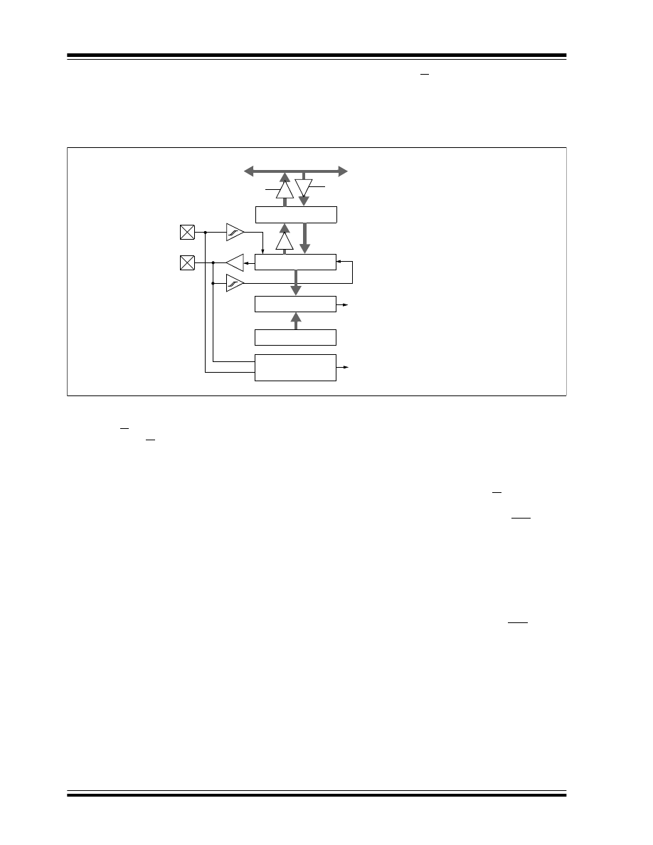
A block diagram of the SSP module for I
2
C Slave mode
. Key control and status bits
required for I
2
C slave communication are provided in
the following Special Function Registers:
• SSPSTAT
• SSPCON
• PIR1 (interrupt flag bits)
• PIE1 (interrupt enable bits)
Some of the bit functions in these registers vary,
depending on whether the SSP module is used for I
2
C
or SPI communications. The functionality of each for
I
2
C mode is described here. For a complete description
of each bit function, refer to the appropriate device data
sheet.
I
2
C SLAVE MODE OPERATION
The MSSP Slave mode operates in one of four modes
selected in the SSPM bits of the SSPCON1 register.
The modes can be divided into 7-bit or 10-bit Address-
ing modes, either with or without Start or Stop bit inter-
rupts enabled. 10-bit Addressing modes operate the
same as 7-bit, with some additional overhead for han-
dling the larger addresses. Modes with Start and Stop
bit interrupts operate the same as the other modes with
SSPIF additionally getting set upon detection of a Start,
Restart or Stop condition.
The SSPADD register contains the Slave mode
address. The first byte received after a Start or Restart
condition is compared against the value stored in this
register. If the byte matches, the value is loaded into
the SSPBUF register and an interrupt is generated. If
the value does not match, the module goes Idle and no
indication is given to the software that anything
happened.
In 7-bit Addressing mode, the LSb of the received data
byte is ignored when determining if there is an address
match. The LSb, which is the R/W bit, will be used later
to determine whether a read or write command was
issued. 7-bit Addressing mode is the most commonly
used mode because of its simplicity.
In 10-bit Addressing mode, the first received byte is
compared to the binary value of ‘1 1 1 1 0 A9 A8
0’. A9 and A8 are the two MSbs of the 10-bit address
and are stored in bits 2 and 1 of the SSPADD register.
After the acknowledge of the high byte, the UA bit is set
and SCL is held low until the user updates SSPADD
with the low address. The low address byte is clocked
in and all eight bits are compared to the low address
value in SSPADD. Even if there is not an address
match, SSPIF and UA are set and SCL is held low until
SSPADD is updated to receive a high byte again. When
SSPADD is updated, the UA bit is cleared. This
ensures the module is ready to receive the
high-address byte on the next communication. A high
TABLE 1:
I
2
C™ BUS TERMS
Term
Description
Transmitter
The device which shifts data out
onto the bus.
Receiver
The device which shifts data in from
the bus.
Master
The device that initiates a transfer,
generates clock signals and
terminates a transfer.
Slave
The device addressed by the
master.
Multi-master
A bus with more than one device
that can initiate data transfers.
Arbitration
Procedure to ensure that only one
master at a time controls the bus.
Winning arbitration ensures that the
message is not corrupted.
Synchroniza-
tion
Procedure to synchronize the
clocks of two or more devices on
the bus.
Idle
No master is controlling the bus,
and both SDA and SCL lines are
high.
Active
Any time one or more master
devices are controlling the bus.
Addressed
Slave
Slave device that has received a
matching address and is actively
being clocked by a master.
Matching
Address
Address byte that is clocked into a
slave that matches the value stored
in SSPADD.
Write Request
Slave receives a matching address
with R/W bit clear, and is ready to
clock in data.
Read Request
Master sends an address byte with
the R/W bit set, indicating that it
wishes to clock data out of the
Slave.
Clock Stretch-
ing
When a device on the bus holds
SCL low to stall communication.
Bus Collision
Any time the SDA line is sampled
low by the module while it is
outputting and expected high state.
AN734
DS00000734C-page 4
2008-2013 Microchip Technology Inc.
and low address match as a write request is required at
the start of all 10-bit addressing communications. A
transmission can be initiated by issuing a Restart once
the slave is addressed, and by clocking in the high
address with the R/W bit set. The slave hardware will
then acknowledge the read request and prepare to
clock out data. This is only valid for a slave after it has
received a complete high and low-address byte match.
FIGURE 3:
PIC16 DEVICES’ MSSP MODULE BLOCK DIAGRAM (
I
2
C™
SLAVE MODE)
Slave Reception (Master Writes to Slave)
When the R/W bit of a matching-received address byte
is cleared, the R/W bit of the SSPSTAT register is
cleared. This indicates that the master device wishes to
write data to the slave. The received address is loaded
into the SSPBUF register and acknowledged. When
the overflow condition exists for a received address,
then no Acknowledge is given. An overflow condition
occurs when a byte is received while the SSPBUF reg-
ister is still holding the previous byte and the BF (Buffer
Full) bit is set. When the overflow condition occurs, the
SSPOV bit of the SSPCON1 register is set. Clock
stretching can help to avoid this condition from occur-
ring. When the SEN bit of the SSPCON2 register is set,
SCL will be held low (clock stretch) following each
received byte. This helps to prevent another byte from
being received. The clock must be released by setting
the CKP bit of the SSPCON1 register. An MSSP inter-
rupt is generated for each transferred data byte. The
interrupt sets the SSPIF flag bit and must be cleared by
software.
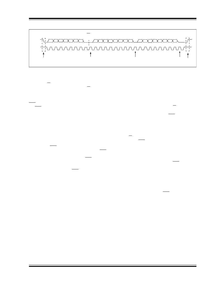
A TYPICAL 7-BIT ADDRESS RECEPTION
This is a step-by-step process of what typically must be
done to accomplish I
2
C communication:
1.
Start bit detected.
2.
The S bit of SSPSTAT is set; the SSPIF flag bit
is set if interrupt on Start detect is enabled.
3.
Matching address with the R/W bit clear is
received.
4.
The slave pulls SDA low, sending an ACK to the
master, and sets SSPIF flag bit.
5.
Software clears the SSPIF flag bit.
6.
Software reads received address from SSPBUF,
clearing the BF bit.
7.
If SEN = 1, Slave software sets the CKP bit to
release the SCL line.
8.
The master clocks out a data byte.
9.
Slave drives SDA low sending an ACK to the
master, and sets the SSPIF bit.
10. Software clears the SSPIF flag bit.
11. Software reads the received byte from SSPBUF,
clearing the BF bit.
12. Steps 8-12 are repeated for all received bytes
from the Master.
13. Master sends Stop condition, setting the P bit of
SSPSTAT, and the bus goes Idle.
Read
Write
SSPSR Register
Match Detect
SSPADD Register
Start and
Stop bit Detect
SSPBUF Register
Internal
Data Bus
Address Match or
Set, Reset
S, P bits (SSPSTAT register)
SCL
Shift
Clock
MSb
LSb
SDA
General Call Detected
2008-2013 Microchip Technology Inc.
DS00000734C-page 5
AN734
FIGURE 4:
TYPICAL I
2
C™ SLAVE RECEPTION (7-BIT ADDRESS)
Slave Transmission (Master Reads From
Slave)
When the R/W bit of the incoming address byte is set
and an address match occurs, the R/W bit of the
SSPSTAT register is set. This indicates that the master
wants to read data from the slave. The received
address is loaded into the SSPBUF register, and an
ACK pulse is sent by the slave on the 9
th
bit. Following
the ACK, slave hardware clears the CKP bit and the
SCL pin is held low (clock stretching). By stretching the
clock, the master will be unable to assert another clock
pulse until the slave is done preparing the transmit
data. The transmit data must be loaded into the
SSPBUF register which also loads the SSPSR register.
Then, the SCL pin should be released by setting the
CKP bit of the SSPCON1 register. The eight data bits
are shifted out on the falling edge of the SCL input. This
ensures that the SDA signal is valid during the SCL
high time. The ACK pulse from the master is latched on
the rising edge of the 9
th
SCL input pulse. This ACK
value is copied to the ACKSTAT bit of the SSPCON2
register. If the ACKSTAT bit is set (not ACK), or the P
(stop) bit is set, the data transfer is complete. The slave
goes Idle and waits for another occurrence of the Start
bit. If the SDA line was low (ACK), the next transmit
data must be loaded into the SSPBUF register. The
SCL pin must be released by setting the CKP bit. An
MSSP interrupt is generated for each data transfer
byte. The SSPIF bit must be cleared by software and
the SSPSTAT register is used to determine the status
of the byte. The SSPIF bit is set on the falling edge of
the 9
th
clock pulse.
A bus collision occurs any time the SDA line is sampled
low by the MSSP module, while it is outputting and
expected high state. If a bus collision is detected and
the SBCDE bit of the SSPCON3 register is set, the
BCLIF flag bit of the PIR register is set. Once a bus
collision is detected, the slave goes Idle and waits to be
addressed again. User software can use the BCLIF flag
bit to handle a slave bus collision.
A write collision occurs when the SSPBUF register was
written to, while the previously written word is still
transmitting. The previous contents of the SSPBUF
register are not changed when a write collision occurs.
When a write collision occurs, the WCOL bit in the
SSPCON1 register will become set. This bit must be
cleared in software.
A TYPICAL 7-BIT ADDRESS TRANSMISSION
1.
Master sends a Start condition.
2.
The S bit of SSPSTAT is set; the SSPIF flag bit
is set if interrupt on Start detect is enabled.
3.
Matching address with the R/W bit set is
received by the Slave, setting the SSPIF flag bit.
4.
Slave hardware generates an ACK and sets the
SSPIF flag bit.
5.
SSPIF flag bit is cleared by user.
6.
Software reads the received address from
SSPBUF, clearing the BF bit.
7.
R/W is set so CKP was automatically cleared
after the ACK.
8.
The slave software loads the transmit data into
SSPBUF.
9.
The CKP bit is set releasing SCL, allowing the
master to clock the data out of the slave.
10. The SSPIF flag bit is set after the ACK response
from the master is loaded into the ACKSTAT bit.
11. The SSPIF flag bit is cleared.
12. The slave software checks the ACKSTAT bit to
see if the master wants to clock out more data.
13. Steps 9-13 are repeated for each transmitted
byte.
14. If the master sends a not ACK, the clock is not
held but the SSPIF flag bit is still set.
15. The master sends a Restart condition or a Stop.
16. The slave is no longer addressed and slave
module is Idle.
P
9
8
7
6
5
D0
D1
D2
D3
D4
D5
D6
D7
S
A7 A6 A5 A4 A3 A2 A1
SDA
SCL
1
2
3
4
5
6
7
8
9
1
2
3
4
5
6
7
8
9
1
2
3
4
ACK
Receiving Data
Receiving Data
D0
D1
D2
D3
D4
D5
D6
D7
ACK
R/W = 0
Receiving Address
Start
ACK
Stop
Acknowledge
Clock
Acknowledge
Clock
Acknowledge
Clock
AN734
DS00000734C-page 6
2008-2013 Microchip Technology Inc.
FIGURE 5:
TYPICAL I
2
C™ SLAVE TRANSMISSION (7-BIT ADDRESS)
MSSP Bits that Indicate Module Status
BF (SSPSTAT<0>)
The BF (Buffer Full) bit tells the user whether a byte of
data is currently in the SSP Buffer register, SSPBUF.
This bit is cleared automatically when the SSPBUF
register is read or when a byte to be transmitted is com-
pletely shifted out of the register. The BF bit will
become set under the following circumstances:
• When an address byte is received with the LSb
cleared. This will be the first byte sent by the
master device during an I
2
C write operation.
• Each time a data byte is received during an I
2
C
write to the slave device.
• Each time a byte of data is written to SSPBUF to
be transmitted to the master device. The BF bit
will be cleared automatically when all bits have
been shifted from SSPBUF to the master device.
UA (SSPSTAT<1>)
The UA (Update Address) bit is used only in the 10-bit
Addressing modes. In the 10-bit Addressing mode, an
I
2
C slave address must be sent in two bytes. The upper
half of the 10-bit address (1111 0 A9 A8 0) is first
loaded into SSPADD for initial match detection. This
particular address code is reserved in the I
2
C protocol
for designating the upper half of a 10-bit address.
When an address match occurs, the SSP module will
set the UA bit to indicate that the lower half of the
address should be loaded into SSPADD for match
detection.
R/W (SSPSTAT<2>)
The R/W (Read/Write) bit tells the user whether the
master device is reading from, or writing to, the slave
device. This bit reflects the state of the LSb in the
address byte that is sent by the master. The state of the
R/W bit is only valid for the duration of a particular I
2
C
message and will be reset by a Stop condition, Start
condition or a NACK from the master device.
S (SSPSTAT<3>)
The S (Start) bit is set if a Start condition occurred last
on the bus. The state of this bit will be the inverse of the
P (Stop) bit, except when the module is first initialized
and both bits are cleared.
P (SSPSTAT<4>)
The P (Stop) bit is set if a Stop condition occurred last
on the bus. The state of this bit will be the inverse of the
S (Start) bit, except when the module is first initialized
and both bits are cleared. The P bit can be used to
determine when the bus is Idle.
D/A (SSPSTAT<5>)
The D/A (Data/Address) bit indicates whether the last
byte of data received by the SSP module was a data
byte or an address byte. For read operations, the last
byte sent to the master device was a data byte when
the D/A bit is set.
WCOL (SSPCON<7>)
The WCOL (Write Collision) bit indicates that SSPBUF
was written while the previously written word is still
transmitting. The previous contents of SSPBUF are not
changed when the write collision occurs. The WCOL bit
must be cleared in software.
SSPOV (SSPCON<6>)
The SSPOV (SSP Overflow) bit indicates that a new
byte was received while SSPBUF was still holding the
previous data. In this case, the SSP module will not
generate an ACK pulse and SSPBUF will not be
updated with the new data. Regardless of whether the
data is to be used, the user must read SSPBUF when-
ever the BF bit becomes set, to avoid an SSP overflow
condition. The user must read SSPBUF and clear the
SSPOV bit to properly clear an overflow condition. If
the user reads SSPBUF to clear the BF bit, but does
not clear the SSPOV bit, the next byte of data received
will be loaded into SSPBUF but the module will not
generate an ACK pulse.
SSPIF (PIR1<3>)
The SSPIF (SSP Interrupt Flag) bit indicates that an
I
2
C event has completed. The user must poll the status
bits described here to determine what event occurred
and the next action to be taken. The SSPIF bit must be
cleared by the user.
SDA
SCL
A7
A6
A5
A4
A3
A2
A1
ACK
D7
D6
D5
D4
D3
D2
D1
D0
NACK
Transmitting Data
R/W = 1
Receiving Address
1
2
3
4
5
6
7
8
9
1
2
3
4
5
6
7
8
9
P
S
Start
Stop
Acknowledge
Clock
Acknowledge
Clock

2008-2013 Microchip Technology Inc.
DS00000734C-page 7
AN734
MSSP Bits for Module Control
SSPEN (SSPCON<5>)
The SSPEN (SSP Enable) bit enables the SSP module
and configures the appropriate I/O pins as serial port
pins.
CKE (SSPSTAT<6>)
The CKE (Clock Edge) bit has no function when the
SSP module is configured for I
2
C mode and should be
cleared.
SMP (SSPSTAT<7>)
The SMP (Sample Phase) bit has no function when the
SSP module is configured for I
2
C mode and should be
cleared.
CKP (SSPCON<4>)
The CKP (Clock Polarity) bit is used for clock stretching
in the I
2
C protocol. When the CKP bit is cleared, the
slave device holds the SCL pin low so that the master
device on the bus is unable to send clock pulses.
During clock stretching, the master device will attempt
to send clock pulses until the clock line is released by
the slave device.
Clock stretching is useful when the slave device cannot
process incoming bytes quickly enough, or when
SSPBUF needs to be loaded with data to be
transmitted to the master device. The SSP module
performs clock stretching automatically when data is
read by the master device. The CKP bit will be cleared
by the module after the address byte and each
subsequent data byte is read. After SSPBUF is loaded,
the CKP bit must be set in software to release the clock
and allow the next byte to be transferred.
SSPM3:SSPM0 (SSPCON<3:0>)
The SSPM3:SSPM0 (SSP mode) bits are used to
configure the SSP module for the SPI or I
2
C protocols.
For specific values, refer to the appropriate device data
sheet.
SSPIE (PIE1<3>)
The SSPIE (SSP Interrupt Enable) bit enables SSP
interrupts. The appropriate global and peripheral
interrupt enable bits must be set in conjunction with this
bit to allow interrupts to occur.
REFERENCES
UM10204 I
2
C™ Bus Specification and User Manual,
NXP Semiconductors, Rev. 5, 2012,
http://www.nxp.com/documents/user_man-
ual/UM10204.pdf
PIC
®
Mid-Range MCU Family Reference Manual,
Microchip Technology Inc., Document Number –
DS33023
AN735, “Using the PICmicro
®
MSSP Module for
Master I
2
C™ Communications”, Microchip Technology
Inc., Document Number – DS00735
AN578, “Use of the SSP Module in the I
2
C™
Multi-Master Environment”, Microchip Technology Inc.,
Document Number – DS00578

AN734
DS00000734C-page 8
2008-2013 Microchip Technology Inc.
APPENDIX A: SOURCE CODE
EXAMPLES
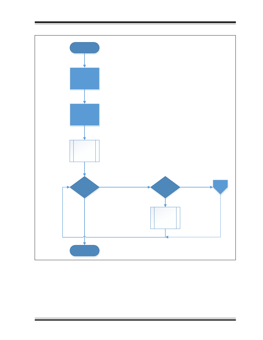
The current revision of this document includes six
separate source code listings to implement the basic
I
2
C slave functions, as described previously.
There are two main versions of the code examples,
version 1 and version 2. Both versions are written in
both C and Assembly for your convenience. Both code
versions are written for the PIC16F1937, but they can
be modified for any mid-range device that has an
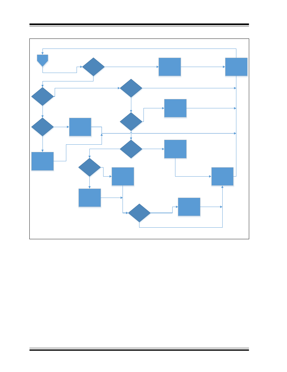
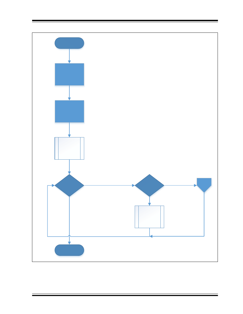
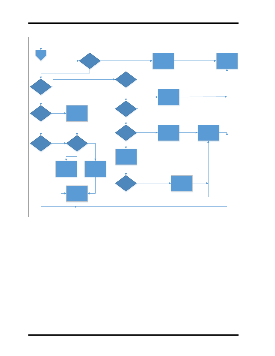
MSSP module. Also included with the example code
are flowcharts, one for each main version of the code,
which should help the user understand the flow of the
code.
The first version, which is referred to as version 1, is
code that can be used in conjunction with the PICkit™
Serial Analyzer. When the PICkit Serial Analyzer is
used, it provides a Graphical User Interface (GUI) that
can be used to test the code. Version 1 code will allow
a user to read from, or write to program memory within
the PIC16F1937 microcontroller. This code uses a 32-
byte array to store data, and each individual location
can be written to, or read from using the GUI. This can
be useful if the user would like to write a value to a spe-
cific memory location that can be used by the micro-
controller for other purposes. For example, if the user
wants to store a value that can be used for speed con-
trol, the value could be written to the first location in the
data array, location ‘0’. The user’s code could then read
from that particular array location and use the data
accordingly. It can also be useful if the user would like
to store data that the master device can read when it
needs to. For example, if the user’s code reads a tem-
perature value, that value can be stored in the array,
and read whenever the master needs the data.
The second version, which is referred to as version 2,
is an example that includes both a master and a slave
code. The master and slave code work together to
transfer data from one to another. Both the master and
slave use two 32-byte arrays to store data. The master
initiates a write (transmission) sequence, which
transfers 32 bytes of data to the slave’s receive array.
After each byte is transferred, a new value is loaded
into the master’s transmit array. This is done so the
user can see that the transmit occurred. After the write
sequence has finished, a Stop sequence is sent to the
slave. Next, a new Start sequence is initialized by the
master, but this time data is read from the slave’s
transmit array. The slave will send 32 bytes of data to
the master’s receive array and, like the master, it will
load a new value into each transmit array location.
Version 2 code should be tested in Debug mode so that
the user can see the file registers easily and monitor
the changes in the arrays. This will require two
separate microcontrollers, one as a master and the
other as a slave.
Source Code Examples:
• I
2
C Master ASM Code Version 2.asm
• I
2
C Master C Code Version 2.c
• I
2
C Slave ASM Code Version 1.asm
• I
2
C Slave ASM Code Version 2.asm
• I
2
C Slave C Code Version 1.c
• I
2
C Slave C Code Version 2.c
Downloadable at
http://www.microchip.com/stellent/idcplg?IdcSer-
vice=SS_GET_PAGE&nodeId=1824&appnote=en011
798
2008-2013 Microchip Technology Inc.
DS00000734C-page 9
AN734
FIGURE A-1:
SLAVE CODE VERSION 1 FLOWCHART (1 OF 2)
Start
Set up variables and
pre-processor
directives
Main()
Clear WDT
Initialize()
End
Is while() true?
Did Interrupt
occur?
ISR routine
YES
NO
YES
NO
AN734
DS00000734C-page 10
2008-2013 Microchip Technology Inc.
FIGURE A-2:
SLAVE CODE VERSION 1 FLOWCHART (2 OF 2)
Is this SSPIF?
Must be Bus
collision. Clear BCLIF
Is this a read
operation
(R/nW =1)?
Clear SSPIF
Is this a write
operation
(R/nW = 0)?
Is this an address
(D/nA = 0)?
Set ‘first’;
Load SSPBUF,
increase index;
Release CLK
Must be data
(D/nA = 1)
Load SSPBUF,
increase index;
Release CLK
Is this an address
(D/nA = 0)?
Set ‘first’;
Read SSPBUF to
clear BF;
Release CLK
Does ‘first’ = 1?
Load index with
SSPBUF value;
Clear ‘first’
Is index < array
size?
Did write
collision occur?
Load array from
SSPBUF, increase
index
Put SSPBUF in junk
Clear WCOL;
Clear SSPBUF
Release CLK
NO
YES
NO
YES
YES
NO
NO
YES
YES
NO
YES
NO
YES
NO
YES
NO
2008-2013 Microchip Technology Inc.
DS00000734C-page 11
AN734
FIGURE A-3:
SLAVE CODE VERSION 2 FLOWCHART (1 OF 2)
Start
Set up variables and
pre-processor
directives
Main()
Clear WDT
Initialize()
End
Is while() true?
Did Interrupt
occur?
ISR routine
YES
NO
YES
NO
AN734
DS00000734C-page 12
2008-2013 Microchip Technology Inc.
FIGURE A-4:
SLAVE CODE VERSION 2 FLOWCHART (2 OF 2)
Is this SSPIF?
Must be Bus
collision. Clear BCLIF
Is this a read
operation
(R/nW =1)?
Clear SSPIF
Is this a write
operation
(R/nW = 0)?
Is this an address
(D/nA = 0)?
Dummy read
SSPBUF;
Clear index
Is this an address
(D/nA = 0)?
Read SSPBUF to
clear BF;
Release CLK
Is index < array
size?
Load index with
SSPBUF value;
Is index < array
size?
Did write
collision occur?
Load SSPBUF with
array value; clear
other array; increase
index
Clear SSPBUF
Clear WCOL;
Clear SSPBUF
Release CLK
NO
YES
NO
YES
YES
NO
NO
YES
YES
NO
YES
NO
YES
NO
YES
NO
Is this data
(D/nA = 1)?
Release CLK
Clear index
YES
NO
ENTER FROM MAIN
RETURN TO MAIN

2008-2013 Microchip Technology Inc.
DS00000734C-page 13
Information contained in this publication regarding device
applications and the like is provided only for your convenience
and may be superseded by updates. It is your responsibility to
ensure that your application meets with your specifications.
MICROCHIP MAKES NO REPRESENTATIONS OR
WARRANTIES OF ANY KIND WHETHER EXPRESS OR
IMPLIED, WRITTEN OR ORAL, STATUTORY OR
OTHERWISE, RELATED TO THE INFORMATION,
INCLUDING BUT NOT LIMITED TO ITS CONDITION,
QUALITY, PERFORMANCE, MERCHANTABILITY OR
FITNESS FOR PURPOSE. Microchip disclaims all liability
arising from this information and its use. Use of Microchip
devices in life support and/or safety applications is entirely at
the buyer’s risk, and the buyer agrees to defend, indemnify and
hold harmless Microchip from any and all damages, claims,
suits, or expenses resulting from such use. No licenses are
conveyed, implicitly or otherwise, under any Microchip
intellectual property rights.
Trademarks
The Microchip name and logo, the Microchip logo, dsPIC,
FlashFlex, K
EE
L
OQ
, K
EE
L
OQ
logo, MPLAB, PIC, PICmicro,
PICSTART, PIC
32
logo, rfPIC, SST, SST Logo, SuperFlash
and UNI/O are registered trademarks of Microchip Technology
Incorporated in the U.S.A. and other countries.
FilterLab, Hampshire, HI-TECH C, Linear Active Thermistor,
MTP, SEEVAL and The Embedded Control Solutions
Company are registered trademarks of Microchip Technology
Incorporated in the U.S.A.
Silicon Storage Technology is a registered trademark of
Microchip Technology Inc. in other countries.
Analog-for-the-Digital Age, Application Maestro, BodyCom,
chipKIT, chipKIT logo, CodeGuard, dsPICDEM,
dsPICDEM.net, dsPICworks, dsSPEAK, ECAN,
ECONOMONITOR, FanSense, HI-TIDE, In-Circuit Serial
Programming, ICSP, Mindi, MiWi, MPASM, MPF, MPLAB
Certified logo, MPLIB, MPLINK, mTouch, Omniscient Code
Generation, PICC, PICC-18, PICDEM, PICDEM.net, PICkit,
PICtail, REAL ICE, rfLAB, Select Mode, SQI, Serial Quad I/O,
Total Endurance, TSHARC, UniWinDriver, WiperLock, ZENA
and Z-Scale are trademarks of Microchip Technology
Incorporated in the U.S.A. and other countries.
SQTP is a service mark of Microchip Technology Incorporated
in the U.S.A.
GestIC and ULPP are registered trademarks of Microchip
Technology Germany II GmbH & Co. KG, a subsidiary of
Microchip Technology Inc., in other countries.
All other trademarks mentioned herein are property of their
respective companies.
© 2008-2013, Microchip Technology Incorporated, Printed in
the U.S.A., All Rights Reserved.
Printed on recycled paper.
ISBN: 9781620773925
Note the following details of the code protection feature on Microchip devices:
•
Microchip products meet the specification contained in their particular Microchip Data Sheet.
•
Microchip believes that its family of products is one of the most secure families of its kind on the market today, when used in the
intended manner and under normal conditions.
•
There are dishonest and possibly illegal methods used to breach the code protection feature. All of these methods, to our
knowledge, require using the Microchip products in a manner outside the operating specifications contained in Microchip’s Data
Sheets. Most likely, the person doing so is engaged in theft of intellectual property.
•
Microchip is willing to work with the customer who is concerned about the integrity of their code.
•
Neither Microchip nor any other semiconductor manufacturer can guarantee the security of their code. Code protection does not
mean that we are guaranteeing the product as “unbreakable.”
Code protection is constantly evolving. We at Microchip are committed to continuously improving the code protection features of our
products. Attempts to break Microchip’s code protection feature may be a violation of the Digital Millennium Copyright Act. If such acts
allow unauthorized access to your software or other copyrighted work, you may have a right to sue for relief under that Act.
Microchip received ISO/TS-16949:2009 certification for its worldwide
headquarters, design and wafer fabrication facilities in Chandler and
Tempe, Arizona; Gresham, Oregon and design centers in California
and India. The Company’s quality system processes and procedures
are for its PIC
®
MCUs and dsPIC
®
DSCs, K
EE
L
OQ
®
code hopping
devices, Serial EEPROMs, microperipherals, nonvolatile memory and
analog products. In addition, Microchip’s quality system for the design
and manufacture of development systems is ISO 9001:2000 certified.
QUALITY MANAGEMENT SYSTEM
CERTIFIED BY DNV
==
ISO/TS 16949
==

DS00000734C-page 14
2008-2013 Microchip Technology Inc.
AMERICAS
Corporate Office
2355 West Chandler Blvd.
Chandler, AZ 85224-6199
Tel: 480-792-7200
Fax: 480-792-7277
Technical Support:
http://www.microchip.com/
support
Web Address:
www.microchip.com
Atlanta
Duluth, GA
Tel: 678-957-9614
Fax: 678-957-1455
Boston
Westborough, MA
Tel: 774-760-0087
Fax: 774-760-0088
Chicago
Itasca, IL
Tel: 630-285-0071
Fax: 630-285-0075
Cleveland
Independence, OH
Tel: 216-447-0464
Fax: 216-447-0643
Dallas
Addison, TX
Tel: 972-818-7423
Fax: 972-818-2924
Detroit
Farmington Hills, MI
Tel: 248-538-2250
Fax: 248-538-2260
Indianapolis
Noblesville, IN
Tel: 317-773-8323
Fax: 317-773-5453
Los Angeles
Mission Viejo, CA
Tel: 949-462-9523
Fax: 949-462-9608
Santa Clara
Santa Clara, CA
Tel: 408-961-6444
Fax: 408-961-6445
Toronto
Mississauga, Ontario,
Canada
Tel: 905-673-0699
Fax: 905-673-6509
ASIA/PACIFIC
Asia Pacific Office
Suites 3707-14, 37th Floor
Tower 6, The Gateway
Harbour City, Kowloon
Hong Kong
Tel: 852-2401-1200
Fax: 852-2401-3431
Australia - Sydney
Tel: 61-2-9868-6733
Fax: 61-2-9868-6755
China - Beijing
Tel: 86-10-8569-7000
Fax: 86-10-8528-2104
China - Chengdu
Tel: 86-28-8665-5511
Fax: 86-28-8665-7889
China - Chongqing
Tel: 86-23-8980-9588
Fax: 86-23-8980-9500
China - Hangzhou
Tel: 86-571-2819-3187
Fax: 86-571-2819-3189
China - Hong Kong SAR
Tel: 852-2943-5100
Fax: 852-2401-3431
China - Nanjing
Tel: 86-25-8473-2460
Fax: 86-25-8473-2470
China - Qingdao
Tel: 86-532-8502-7355
Fax: 86-532-8502-7205
China - Shanghai
Tel: 86-21-5407-5533
Fax: 86-21-5407-5066
China - Shenyang
Tel: 86-24-2334-2829
Fax: 86-24-2334-2393
China - Shenzhen
Tel: 86-755-8864-2200
Fax: 86-755-8203-1760
China - Wuhan
Tel: 86-27-5980-5300
Fax: 86-27-5980-5118
China - Xian
Tel: 86-29-8833-7252
Fax: 86-29-8833-7256
China - Xiamen
Tel: 86-592-2388138
Fax: 86-592-2388130
China - Zhuhai
Tel: 86-756-3210040
Fax: 86-756-3210049
ASIA/PACIFIC
India - Bangalore
Tel: 91-80-3090-4444
Fax: 91-80-3090-4123
India - New Delhi
Tel: 91-11-4160-8631
Fax: 91-11-4160-8632
India - Pune
Tel: 91-20-2566-1512
Fax: 91-20-2566-1513
Japan - Osaka
Tel: 81-6-6152-7160
Fax: 81-6-6152-9310
Japan - Tokyo
Tel: 81-3-6880- 3770
Fax: 81-3-6880-3771
Korea - Daegu
Tel: 82-53-744-4301
Fax: 82-53-744-4302
Korea - Seoul
Tel: 82-2-554-7200
Fax: 82-2-558-5932 or
82-2-558-5934
Malaysia - Kuala Lumpur
Tel: 60-3-6201-9857
Fax: 60-3-6201-9859
Malaysia - Penang
Tel: 60-4-227-8870
Fax: 60-4-227-4068
Philippines - Manila
Tel: 63-2-634-9065
Fax: 63-2-634-9069
Singapore
Tel: 65-6334-8870
Fax: 65-6334-8850
Taiwan - Hsin Chu
Tel: 886-3-5778-366
Fax: 886-3-5770-955
Taiwan - Kaohsiung
Tel: 886-7-213-7828
Fax: 886-7-330-9305
Taiwan - Taipei
Tel: 886-2-2508-8600
Fax: 886-2-2508-0102
Thailand - Bangkok
Tel: 66-2-694-1351
Fax: 66-2-694-1350
EUROPE
Austria - Wels
Tel: 43-7242-2244-39
Fax: 43-7242-2244-393
Denmark - Copenhagen
Tel: 45-4450-2828
Fax: 45-4485-2829
France - Paris
Tel: 33-1-69-53-63-20
Fax: 33-1-69-30-90-79
Germany - Munich
Tel: 49-89-627-144-0
Fax: 49-89-627-144-44
Italy - Milan
Tel: 39-0331-742611
Fax: 39-0331-466781
Netherlands - Drunen
Tel: 31-416-690399
Fax: 31-416-690340
Spain - Madrid
Tel: 34-91-708-08-90
Fax: 34-91-708-08-91
UK - Wokingham
Tel: 44-118-921-5869
Fax: 44-118-921-5820
Worldwide Sales and Service
11/29/12
Document Outline
- Introduction
- The I2C Bus Specification
- The MSSP Module
- I2C Slave Mode Operation
- References
- Appendix A: Source Code Examples
- Trademarks
- Worldwide Sales
Wyszukiwarka
Podobne podstrony:
Gor±czka o nieznanej etiologii
02 VIC 10 Days Cumulative A D O Nieznany (2)
Abolicja podatkowa id 50334 Nieznany (2)
45 sekundowa prezentacja w 4 ro Nieznany (2)
4 LIDER MENEDZER id 37733 Nieznany (2)
Mechanika Plynow Lab, Sitka Pro Nieznany
katechezy MB id 233498 Nieznany
2012 styczen OPEXid 27724 Nieznany
metro sciaga id 296943 Nieznany
Mazowieckie Studia Humanistyczn Nieznany (11)
cw 16 odpowiedzi do pytan id 1 Nieznany
perf id 354744 Nieznany
DO TEL! 5= Genetyka nadci nieni Nieznany
Opracowanie FINAL miniaturka id Nieznany
3 Podstawy fizyki polprzewodnik Nieznany (2)
interbase id 92028 Nieznany
Mbaku id 289860 Nieznany
więcej podobnych podstron