1
®
FN2867.9
CAUTION: These devices are sensitive to electrostatic discharge; follow proper IC Handling Procedures.
1-888-INTERSIL or 1-888-468-3774
|
Intersil (and design) is a registered trademark of Intersil Americas Inc.
Copyright © Intersil Americas Inc. 2002, 2004, 2005, 2006. All Rights Reserved
All other trademarks mentioned are the property of their respective owners.
ICM7555, ICM7556
General Purpose Timers
The ICM7555 and ICM7556 are CMOS RC timers providing
significantly improved performance over the standard
SE/NE 555/6 and 355 timers, while at the same time being
direct replacements for those devices in most applications.
Improved parameters include low supply current, wide
operating supply voltage range, low THRESHOLD,
TRIGGER and RESET currents, no crowbarring of the
supply current during output transitions, higher frequency
performance and no requirement to decouple CONTROL
VOLTAGE for stable operation.
Specifically, the ICM7555 and ICM7556 are stable
controllers capable of producing accurate time delays or
frequencies. The ICM7556 is a dual ICM7555, with the two
timers operating independently of each other, sharing only
V+ and GND. In the one shot mode, the pulse width of each
circuit is precisely controlled by one external resistor and
capacitor. For astable operation as an oscillator, the free
running frequency and the duty cycle are both accurately
controlled by two external resistors and one capacitor. Unlike
the regular bipolar SE/NE 555/6 devices, the CONTROL
VOLTAGE terminal need not be decoupled with a capacitor.
The circuits are triggered and reset on falling (negative)
waveforms, and the output inverter can source or sink
currents large enough to drive TTL loads, or provide minimal
offsets to drive CMOS loads.
Features
• Exact Equivalent in Most Cases for SE/NE555/556 or
TLC555/556
• Low Supply Current
- ICM7555 . . . . . . . . . . . . . . . . . . . . . . . . . . . . . . . . 60
μA
- ICM7556 . . . . . . . . . . . . . . . . . . . . . . . . . . . . . . . 120
μA
• Extremely Low Input Currents . . . . . . . . . . . . . . . . . 20pA
• High Speed Operation . . . . . . . . . . . . . . . . . . . . . . . 1MHz
• Guaranteed Supply Voltage Range . . . . . . . . . 2V to 18V
• Temperature Stability . . . . . . . . . . . . 0.005%/°C at +25°C
• Normal Reset Function - No Crowbarring of Supply During
Output Transition
• Can be Used with Higher Impedance Timing Elements
than Regular 555/6 for Longer RC Time Constants
• Timing from Microseconds through Hours
• Operates in Both Astable and Monostable Modes
• Adjustable Duty Cycle
• High Output Source/Sink Driver can Drive TTL/CMOS
• Outputs have Very Low Offsets, HI and LO
• Pb-Free Plus Anneal Available (RoHS Compliant)
Applications
• Precision Timing
• Pulse Generation
• Sequential Timing
• Time Delay Generation
• Pulse Width Modulation
• Pulse Position Modulation
• Missing Pulse Detector
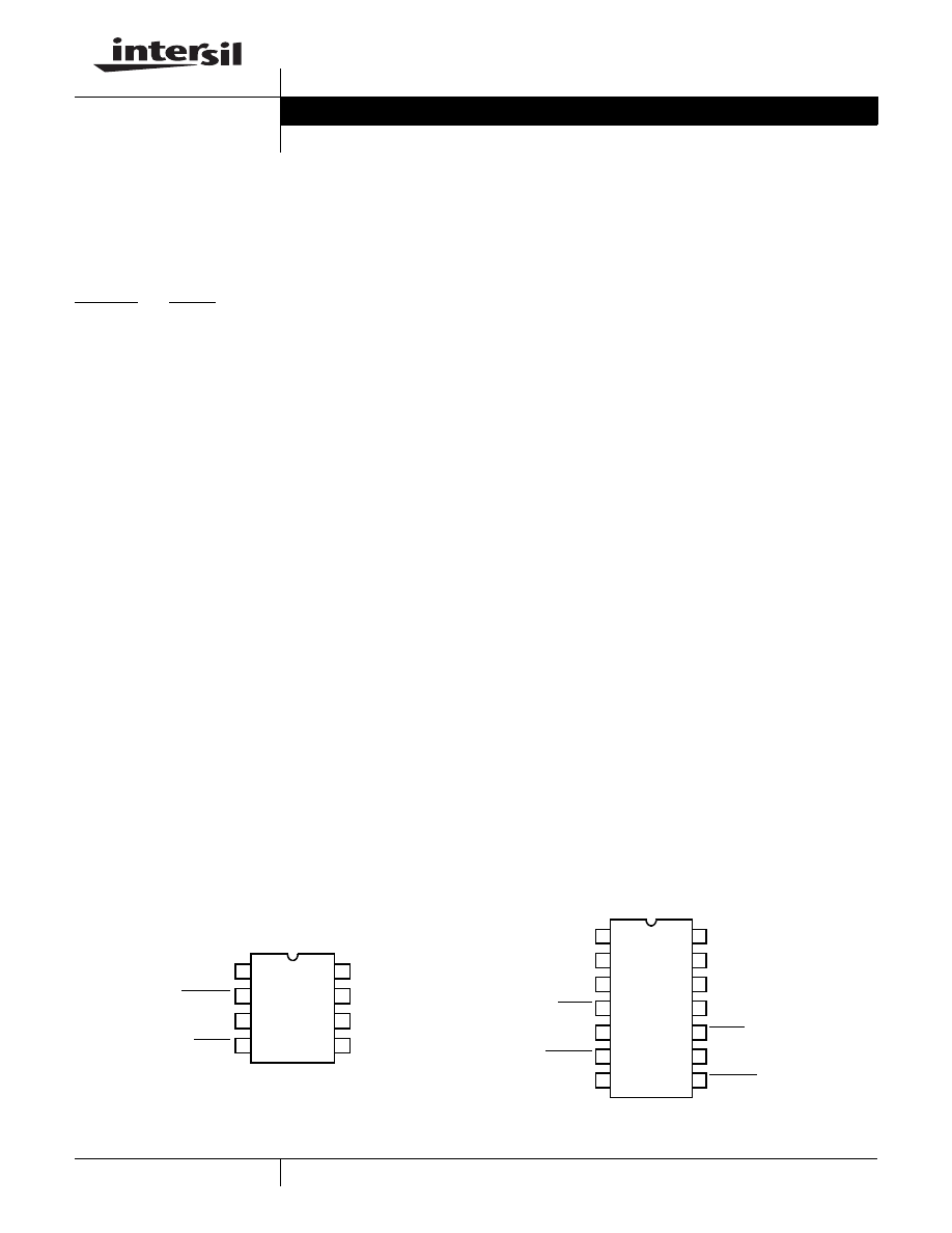
Pinouts
ICM7555 (8 LD PDIP, SOIC)
TOP VIEW
ICM7556 (14 LD PDIP, CERDIP)
TOP VIEW
GND
TRIGGER
OUTPUT
RESET
1
2
3
4
8
7
6
5
V
DD
DISCHARGE
THRESHOLD
CONTROL
VOLTAGE
DISCHARGE
THRESH-
CONTROL
RESET
OUTPUT
TRIGGER
GND
V
DD
DISCHARGE
THRESHOLD
CONTROL
RESET
OUTPUT
TRIGGER
1
2
3
4
5
6
7
14
13
12
11
10
9
8
VOLTAGE
VOLTAGE
OLD
Data Sheet
August 24, 2006
2
FN2867.9
August 24, 2006
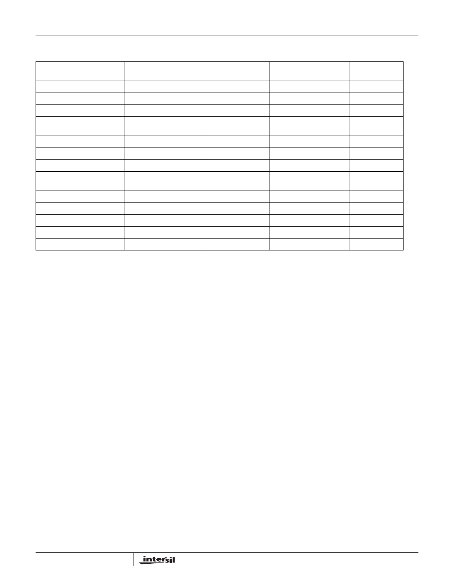
Ordering Information
PART NUMBER
PART MARKING
TEMP. RANGE
(°C)
PACKAGE
PKG. DWG. #
ICM7555CBA
7555 CBA
0 to +70
8 Ld SOIC
M8.15
ICM7555CBA-T
7555 CBA
0 to +70
8 Ld SOIC Tape and Reel
M8.15
ICM7555CBAZ (Note)
7555 CBAZ
0 to +70
8 Ld SOIC (Pb-free)
M8.15
ICM7555CBAZ-T (Note)
7555 CBAZ
0 to +70
8 Ld SOIC (Pb-free)
Tape and Reel
M8.15
ICM7555IBA
7555 IBA
-25 to +85
8 Ld SOIC
M8.15
ICM7555IBAT
7555 IBA
-25 to +85
8 Ld SOIC Tape and Reel
M8.15
ICM7555IBAZ (Note)
7555 IBAZ
-25 to +85
8 Ld SOIC (Pb-free)
M8.15
ICM7555IBAZ-T (Note)
7555 IBAZ
-25 to +85
8 Ld SOIC (Pb-free)
Tape and Reel
M8.15
ICM7555IPA
7555 IPA
-25 to +85
8 Ld PDIP
E8.3
ICM7555IPAZ (Note)
7555 IPAZ
-25 to +85
8 Ld PDIP** (Pb-free)
E8.3
ICM7556IPD
ICM7556IPD
-25 to +85
14 Ld PDIP
E14.3
ICM7556IPDZ (Note)
ICM7556IPDZ
-25 to +85
14 Ld PDIP** (Pb-free)
E14.3
ICM7556MJD
ICM7556MJD
-55 to +125
14 Ld Cerdip
F14.3
**Pb-free PDIPs can be used for through hole wave solder processing only. They are not intended for use in Reflow solder processing
applications.
NOTE: Intersil Pb-free products employ special Pb-free material sets; molding compounds/die attach materials and 100% matte tin plate
termination finish, which are RoHS compliant and compatible with both SnPb and Pb-free soldering operations. Intersil Pb-free products are
MSL classified at Pb-free peak reflow temperatures that meet or exceed the Pb-free requirements of IPC/JEDEC J STD-020.
ICM7555, ICM7556
3
FN2867.9
August 24, 2006
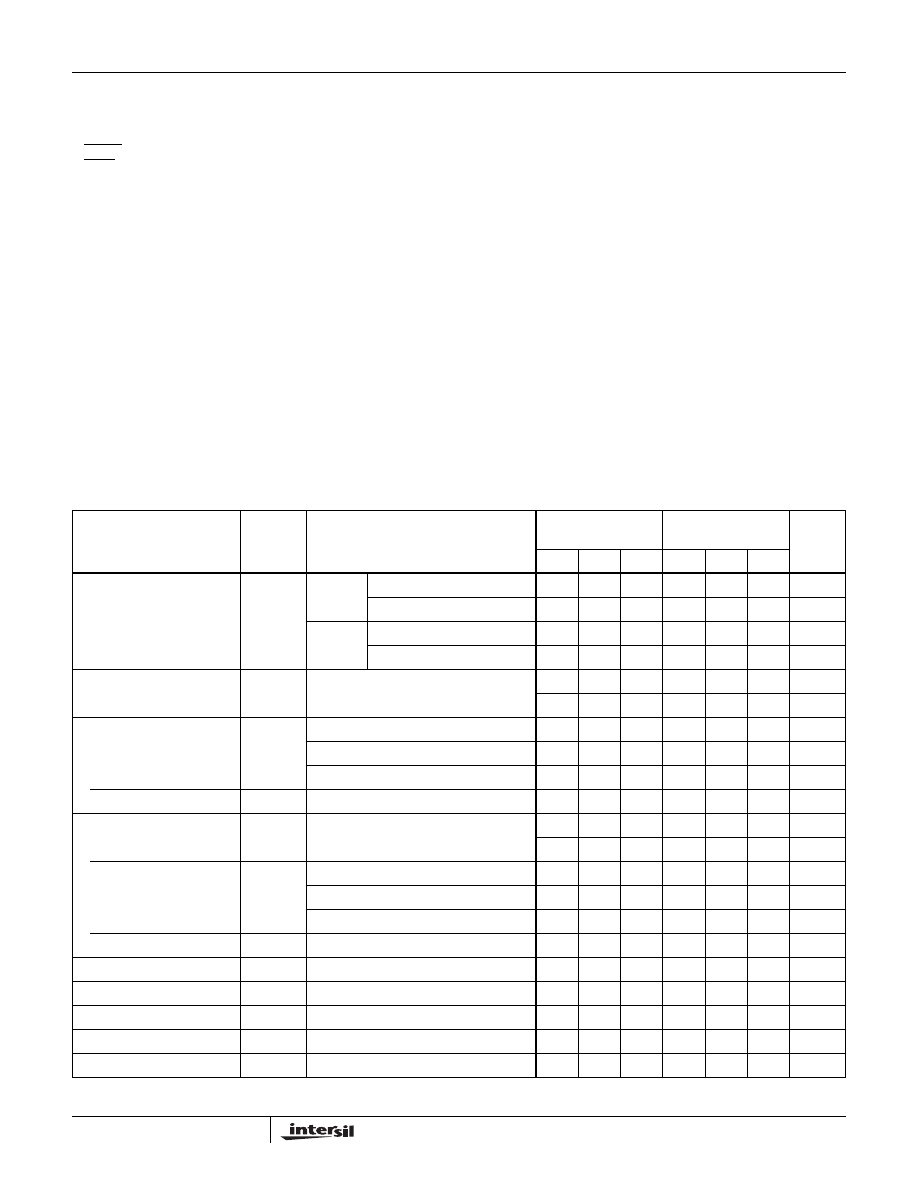
Absolute Maximum Ratings
Thermal Information
Supply Voltage. . . . . . . . . . . . . . . . . . . . . . . . . . . . . . . . . . . . . .+18V
Input Voltage
Trigger, Control Voltage, Threshold,
Reset (Note 1) . . . . . . . . . . . . . . . . . . . . . V+ +0.3V to GND -0.3V
Output Current . . . . . . . . . . . . . . . . . . . . . . . . . . . . . . . . . . . . 100mA
Operating Conditions
Temperature Range
ICM7555C . . . . . . . . . . . . . . . . . . . . . . . . . . . . . . . . 0°C to +70°C
ICM7555I, ICM7556I . . . . . . . . . . . . . . . . . . . . . . -25°C to +85°C
ICM7556M . . . . . . . . . . . . . . . . . . . . . . . . . . . . . -55°C to +125°C
Thermal Resistance (Typical, Note 2)
θ
JA
(°C/W)
θ
JC
(°C/W)
14 Lead CERDIP Package. . . . . . . . . .
80
24
14 Lead PDIP Package* . . . . . . . . . . .
115
N/A
8 Lead PDIP Package* . . . . . . . . . . . .
130
N/A
8 Lead SOIC Package . . . . . . . . . . . . .
170
N/A
Maximum Junction Temperature (Hermetic Package) . . . . . . . +175°C
Maximum Junction Temperature (Plastic Package) . . . . . . . +150°C
Maximum Storage Temperature Range . . . . . . . . -65°C to +150°C
Maximum Lead Temperature (Soldering 10s) . . . . . . . . . . . +300°C
(SOIC - Lead Tips Only)
* Pb-free PDIPs can be used for through hole wave solder
processing only. They are not intended for use in Reflow solder
processing applications.
CAUTION: Stresses above those listed in “Absolute Maximum Ratings” may cause permanent damage to the device. This is a stress only rating and operation of the
device at these or any other conditions above those indicated in the operational sections of this specification is not implied.
NOTES:
1. Due to the SCR structure inherent in the CMOS process used to fabricate these devices, connecting any terminal to a voltage greater than
V+ +0.3V or less than V- -0.3V may cause destructive latchup. For this reason it is recommended that no inputs from external sources not
operating from the same power supply be applied to the device before its power supply is established. In multiple supply systems, the supply
of the ICM7555 and ICM7556 must be turned on first.
2.
θ
JA
is measured with the component mounted on a low effective thermal conductivity test board in free air. See Tech Brief 379 for details.
Electrical Specifications
Applies to ICM7555 and ICM7556, unless otherwise specified
PARAMETER
SYMBOL
TEST CONDITIONS
T
A
= +25°C
(NOTE 4)
-55°C TO
+125°C
UNITS
MIN
TYP
MAX
MIN
TYP
MAX
Static Supply Current
I
DD
ICM7555
V
DD
= 5V
40
200
300
μA
V
DD
= 15V
60
300
300
μA
ICM7556
V
DD
= 5V
80
400
600
μA
V
DD
= 15V
120
600
600
μA
Monostable Timing Accuracy
R
A
= 10K, C = 0.1
μF, V
DD
= 5V
2
%
858
1161
μs
Drift with Temperature
(Note 3)
V
DD
= 5V
150
ppm/
°C
V
DD
= 10V
200
ppm/
°C
V
DD
= 15V
250
ppm/
°C
Drift with Supply (Note 3)
V
DD
= 5V to 15V
0.5
0.5
%/V
Astable Timing Accuracy
R
A
= R
B
= 10K, C = 0.1
μF, V
DD
= 5V
2
%
1717
2323
μs
Drift with Temperature
(Note 3)
V
DD
= 5V
150
ppm/
°C
V
DD
= 10V
200
ppm/
°C
V
DD
= 15V
250
ppm/
°C
Drift with Supply (Note 3)
V
DD
= 5V to 15V
0.5
0.5
%/V
Threshold Voltage
V
TH
V
DD
= 15V
62
67
71
61
72
% V
DD
Trigger Voltage
V
TRIG
V
DD
= 15V
28
32
36
27
37
% V
DD
Trigger Current
I
TRIG
V
DD
= 15V
10
50
nA
Threshold Current
I
TH
V
DD
= 15V
10
50
nA
Control Voltage
V
CV
V
DD
= 15V
62
67
71
61
72
% V
DD
ICM7555, ICM7556
4
FN2867.9
August 24, 2006
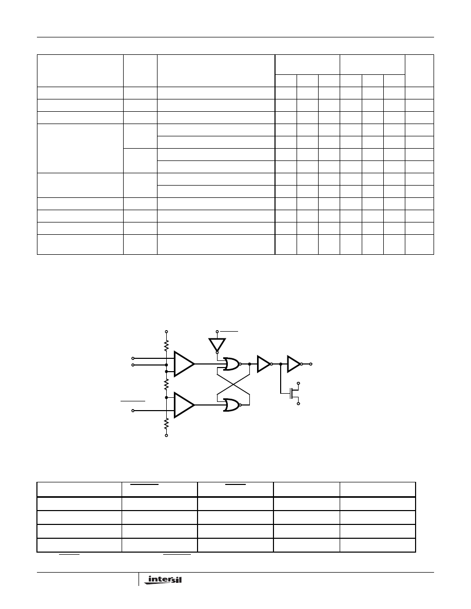
Functional Diagram
Reset Voltage
V
RST
V
DD
= 2V to 15V
0.4
1.0
0.2
1.2
V
Reset Current
I
RST
V
DD
= 15V
10
50
nA
Discharge Leakage
I
DIS
V
DD
= 15V
10
50
nA
Output Voltage
V
OL
V
DD
= 15V, I
SINK
= 20mA
0.4
1.0
1.25
V
V
DD
= 5V, I
SINK
= 3.2mA
0.2
0.4
0.5
V
V
OH
V
DD
= 15V, I
SOURCE
= 0.8mA
14.3
14.6
14.2
V
V
DD
= 5V, I
SOURCE
= 0.8mA
4.0
4.3
3.8
V
Discharge Output Voltage
V
DIS
V
DD
= 5V, I
SINK
= 15mA
0.2
0.4
0.6
V
V
DD
= 15V, I
SINK
= 15mA
0.4
V
Supply Voltage (Note 3)
V
DD
Functional Operation
2.0
18.0
3.0
16.0
V
Output Rise Time (Note 3)
t
R
R
L
= 10M, C
L
= 10pF, V
DD
= 5V
75
ns
Output Fall Time (Note 3)
t
F
R
L
= 10M, C
L
= 10pF, V
DD
= 5V
75
ns
Oscillator Frequency
(Note 3)
f
MAX
V
DD
= 5V, R
A
= 470
Ω, R
B
= 270
Ω,
C = 200pF
1
MHz
NOTES:
3. These parameters are based upon characterization data and are not tested.
4. Applies only to military temperature range product (M suffix).
Electrical Specifications
Applies to ICM7555 and ICM7556, unless otherwise specified (Continued)
PARAMETER
SYMBOL
TEST CONDITIONS
T
A
= +25°C
(NOTE 4)
-55°C TO
+125°C
UNITS
MIN
TYP
MAX
MIN
TYP
MAX
+
-
THRESHOLD
CONTROL
VOLTAGE
6
5
3
1
+
-
TRIGGER
2
COMPARATOR
R
GND
B
COMPARATOR
A
R
V
DD
8
OUTPUT
7
1
n
DISCHARGE
OUTPUT
DRIVERS
FLIP-FLOP
RESET
4
R
NOTE:
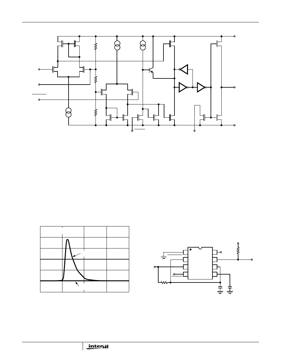
This functional diagram reduces the circuitry down to its simplest equivalent components. Tie down unused inputs.
TRUTH TABLE
THRESHOLD VOLTAGE
TRIGGER VOLTAGE
RESET
OUTPUT
DISCHARGE SWITCH
Don’t Care
Don’t Care
Low
Low
On
>
2
/
3
(V+)
>
1
/
3
(V+)
High
Low
On
<
2
/
3
(V+)
>
1
/
3
(V+)
High
Stable
Stable
Don’t Care
<
1
/
3
(V+)
High
High
Off
NOTE: RESET will dominate all other inputs: TRIGGER will dominate over THRESHOLD.
ICM7555, ICM7556
5
FN2867.9
August 24, 2006
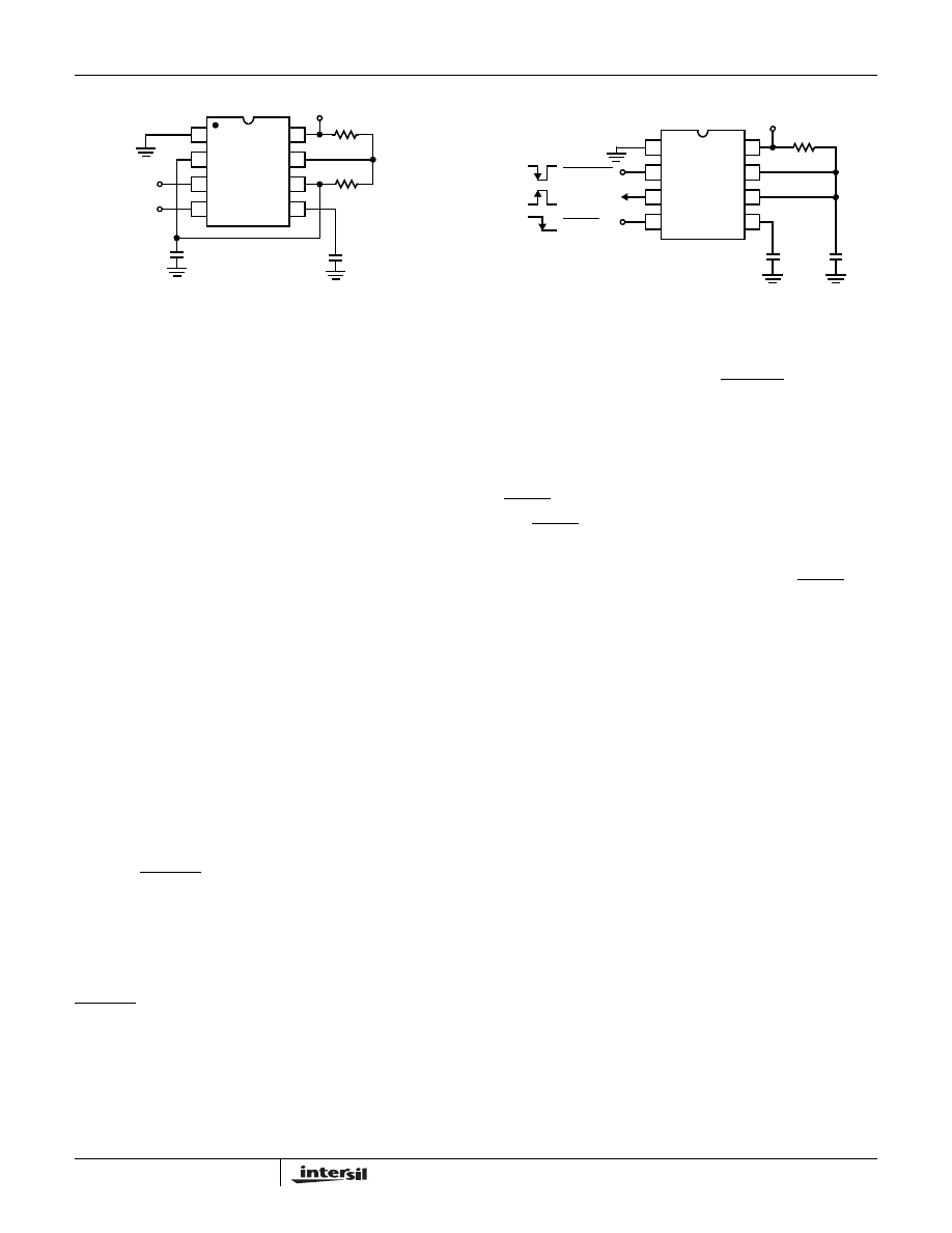
Schematic Diagram
Application Information
General
The ICM7555 and ICM7556 devices are, in most instances,
direct replacements for the NE/SE 555/6 devices. However,
it is possible to effect economies in the external component
count using the ICM7555 and ICM7556. Because the bipolar
NE/SE 555/6 devices produce large crowbar currents in the
output driver, it is necessary to decouple the power supply
lines with a good capacitor close to the device. The ICM7555
and ICM7556 devices produce no such transients. See
Figure 1.
The ICM7555 and ICM7556 produce supply current spikes
of only 2mA - 3mA instead of 300mA - 400mA and supply
decoupling is normally not necessary. Also, in most
instances, the CONTROL VOLTAGE decoupling capacitors
are not required since the input impedance of the CMOS
comparators on chip are very high. Thus, for many
applications, two capacitors can be saved using an ICM7555
and three capacitors with an ICM7556.
POWER SUPPLY CONSIDERATIONS
Although the supply current consumed by the ICM7555 and
ICM7556 devices is very low, the total system supply current
can be high unless the timing components are high
impedance. Therefore, use high values for R and low values
for C in Figures 2A, 2B, and 3.
RESET
DISCHARGE
TRIGGER
THRESHOLD
GND
OUTPUT
CONTROL
VOLTAGE
R
N
N
NPN
P
R
R
V
DD
N
N
N
N
N
P
P
N
N
P
P
P
R = 100k
Ω ±20% (TYP)
TIME (ns)
400
800
600
200
0
0
100
200
300
400
500
SUPP
L
Y
CURRENT (
m
A)
SE/NE555
T
A
= 25°C
ICM7555/56
FIGURE 1. SUPPLY CURRENT TRANSIENT COMPARED WITH
A STANDARD BIPOLAR 555 DURING AN OUTPUT
TRANSITION
GND
TRIGGER
OUTPUT
RESET
1
2
3
4
8
7
6
5
V
DD
DISCHARGE
THRESHOLD
CONTROL
VOLTAGE
V
DD
10K
A
LTER
NAT
E O
U
TPUT
OPTIONAL
CAPACITOR
C
V
DD
R
FIGURE 2A. ASTABLE OPERATION
ICM7555, ICM7556
6
FN2867.9
August 24, 2006
OUTPUT DRIVE CAPABILITY
The output driver consists of a CMOS inverter capable of
driving most logic families including CMOS and TTL. As
such, if driving CMOS, the output swing at all supply
voltages will equal the supply voltage. At a supply voltage of
4.5V or more, the ICM7555 and ICM7556 will drive at least
two standard TTL loads.
ASTABLE OPERATION
The circuit can be connected to trigger itself and free run as
a multivibrator, see Figure 2A. The output swings from rail to
rail, and is a true 50% duty cycle square wave. (Trip points
and output swings are symmetrical.) Less than a 1%
frequency variation is observed over a voltage range of +5V
to +15V.
The timer can also be connected as shown in Figure 2B. In this
circuit, the frequency is:
The duty cycle is controlled by the values of R
A
and R
B
, by the
equation:
MONOSTABLE OPERATION
In this mode of operation, the timer functions as a one-shot.
See Figure 3. Initially the external capacitor (C) is held
discharged by a transistor inside the timer. Upon application of
a negative TRIGGER pulse to pin 2, the internal flip-flop is set
which releases the short circuit across the external capacitor
and drives the OUTPUT high. The voltage across the capacitor
now increases exponentially with a time constant t = R
A
C.
When the voltage across the capacitor equals
2
/
3
V+, the
comparator resets the flip-flop, which in turn discharges the
capacitor rapidly and also drives the OUTPUT to its low state.
TRIGGER must return to a high state before the OUTPUT can
return to a low state.
CONTROL VOLTAGE
The CONTROL VOLTAGE terminal permits the two trip
voltages for the THRESHOLD and TRIGGER internal
comparators to be controlled. This provides the possibility of
oscillation frequency modulation in the astable mode or even
inhibition of oscillation, depending on the applied voltage. In
the monostable mode, delay times can be changed by
varying the applied voltage to the CONTROL VOLTAGE pin.
RESET
The RESET terminal is designed to have essentially the
same trip voltage as the standard bipolar 555/6, i.e., 0.6V to
0.7V. At all supply voltages it represents an extremely high
input impedance. The mode of operation of the RESET
function is, however, much improved over the standard
bipolar NE/SE 555/6 in that it controls only the internal flip-
flop, which in turn controls simultaneously the state of the
OUTPUT and DISCHARGE pins. This avoids the multiple
threshold problems sometimes encountered with slow falling
edges in the bipolar devices.
OUTPUT
1
2
3
4
8
7
6
5
V
DD
OPTIONAL
CAPACITOR
C
V
DD
R
A
R
B
FIGURE 2B. ALTERNATE ASTABLE CONFIGURATION
f
1
1.4 RC
------------------
=
(EQ. 1)
f
1.44 RA 2RB
+
(
)
⁄
C
=
(EQ. 2)
D
RA RB
+
(
) RA 2RB
+
(
)
⁄
=
(EQ. 3)
TRIGGER
OUTPUT
RESET
1
2
3
4
8
7
6
5
V
DD
DISCHARGE
THRESHOLD
CONTROL
VOLTAGE
OPTIONAL
CAPACITOR
C
V
DD
≤18V
R
A
ICM7555
t
OUTPUT
= -ln
(1/3)
R
A
C = 1.1R
A
C
FIGURE 3. MONOSTABLE OPERATION
ICM7555, ICM7556
7
FN2867.9
August 24, 2006
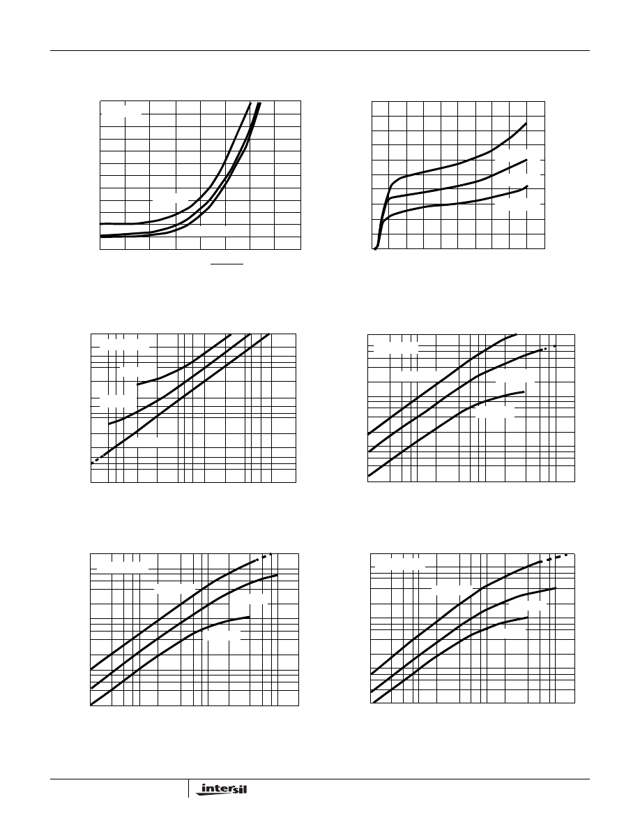
Typical Performance Curves
FIGURE 4. MINIMUM PULSE WIDTH REQUIRED FOR
TRIGGERING
FIGURE 5. SUPPLY CURRENT vs SUPPLY VOLTAGE
FIGURE 6. OUTPUT SOURCE CURRENT vs OUTPUT VOLTAGE
FIGURE 7. OUTPUT SINK CURRENT vs OUTPUT VOLTAGE
FIGURE 8. OUTPUT SINK CURRENT vs OUTPUT VOLTAGE
FIGURE 9. OUTPUT SINK CURRENT vs OUTPUT VOLTAGE
T
A
= 25°C
V
DD
= 2V
V
DD
= 18V
LOWEST VOLTAGE LEVEL OF
TRIGGER PULSE (%V
DD
)
V
DD
= 5V
MINI
MUM
P
U
LSE WIDTH (ns)
0
10
20
30
40
0
1200
1100
1000
900
800
700
600
500
400
300
200
100
SUPPLY VOLTAGE (V)
T
A
= 25°C
SUP
P
L
Y
CURRENT
(I
C
M
7
555)
(
μA)
SUP
P
L
Y
CURRENT
(I
C
M
7
556)
(
μA)
T
A
= -20°C
T
A
= 70°C
0
2
4
6
8
10
12
14
16
18
20
0
200
180
160
140
120
100
80
60
40
20
400
360
320
280
240
200
160
120
80
40
0
T
A
= 25°C
V
DD
= 2V
V
DD
= 5V
V
DD
= 18V
OU
TP
UT
SOUR
CE
CURRENT (m
A)
-100
-10.0
-1.0
-0.1
-0.01
-0.1
-1.0
-10
OUTPUT VOLTAGE REFERENCED TO V
DD
(V)
T
A
= -20°C
OUTPUT LOW VOLTAGE (V)
V
DD
= 2V
V
DD
= 5V
V
DD
= 18V
OUTPUT SINK
CURRENT
(m
A)
0.01
0.1
1.0
10.0
0.1
100
10.0
1.0
T
A
= 25°C
OUTPUT LOW VOLTAGE (V)
V
DD
= 2V
V
DD
= 5V
V
DD
= 18V
OUTPUT
S
INK CUR
RE
NT
(mA)
0.01
0.1
1.0
10.0
0.1
100
10.0
1.0
T
A
= 70°C
OUTPUT LOW VOLTAGE (V)
V
DD
= 2V
V
DD
= 5V
V
DD
= 18V
OU
TP
U
T
SINK
CURRENT (m
A)
0.01
0.1
1.0
10.0
0.1
100
10.0
1.0
ICM7555, ICM7556
8
FN2867.9
August 24, 2006
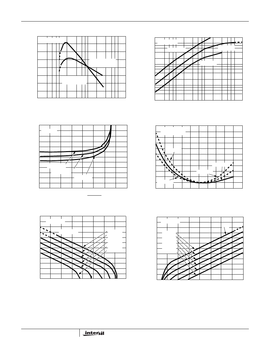
FIGURE 10. NORMALIZED FREQUENCY STABILITY IN THE
ASTABLE MODE vs SUPPLY VOLTAGE
FIGURE 11. DISCHARGE OUTPUT CURRENT vs DISCHARGE
OUTPUT VOLTAGE
FIGURE 12. PROPAGATION DELAY vs VOLTAGE LEVEL OF
TRIGGER PULSE
FIGURE 13. NORMALIZED FREQUENCY STABILITY IN THE
ASTABLE MODE vs TEMPERATURE
FIGURE 14. FREE RUNNING FREQUENCY vs R
A
, R
B
AND C
FIGURE 15. TIME DELAY IN THE MONOSTABLE MODE vs
R
A
AND C
Typical Performance Curves
(Continued)
SUPPLY VOLTAGE (V)
T
A
= 25°C
NORM
ALIZE
D
FRE
Q
UE
NCY
DEV
IATION (
%
)
R
A
= R
B
= 10M
Ω
0.1
1.0
10.0
100.0
8
8
6
4
2
0
2
4
6
C = 100pF
R
A
= R
B
= 10k
Ω
C = 0.1
μF
T
A
= 25°C
DISCHARGE LOW VOLTAGE (V)
V
DD
= 2V
V
DD
= 5V
V
DD
= 18V
DIS
CHA
RGE SINK
CURRENT
(m
A)
0.01
0.1
1.0
10.0
0.1
100
10.0
1.0
T
A
= 25°C
LOWEST VOLTAGE LEVEL OF
TRIGGER PULSE (%V
DD
)
V
DD
= 5V
P
R
OP
AGA
T
ION DELA
Y (ns)
0
10
20
30
40
0
600
500
400
300
200
100
T
A
= 70°C
T
A
= -20°C
TEMPERATURE (°C)
NORMALIZED FREQUE
N
C
Y
DEV
IA
T
ION
(%
)
0
60
80
-0.1
+0.1
0
R
A
= R
B
= 10k
Ω
C = 0.1
μF
40
20
-20
+0.2
+0.3
+0.4
+0.5
+0.6
+0.7
+0.8
+0.9
+1.0
V
DD
= 2V
V
DD
= 5V
V
DD
= 18V
V
DD
= 2V
T
A
= 25°C
FREQUENCY (Hz)
(R
A
+ 2R
B
)
1k
Ω
10k
Ω
100k
Ω
1M
Ω
10M
Ω
100M
Ω
10
0.1
1
100
1k
10k
100k
1M
10M
CAP
ACIT
ANCE (
F
)
1.0
100m
10m
1m
100
μ
10
μ
1
μ
100n
10n
1n
100p
10p
1p
TIME DELAY (s)
1k
Ω
10k
Ω
100k
Ω
1M
Ω
10M
Ω
100M
Ω
10
μ
100n
1
μ
100
μ
1m
10m
100m
1
10
CAP
ACIT
ANCE (
F
)
1.0
100m
10m
1m
100
μ
10
μ
1
μ
100n
10n
1n
100p
10p
1p
R
A
T
A
= 25°C
ICM7555, ICM7556
9
FN2867.9
August 24, 2006
ICM7555, ICM7556
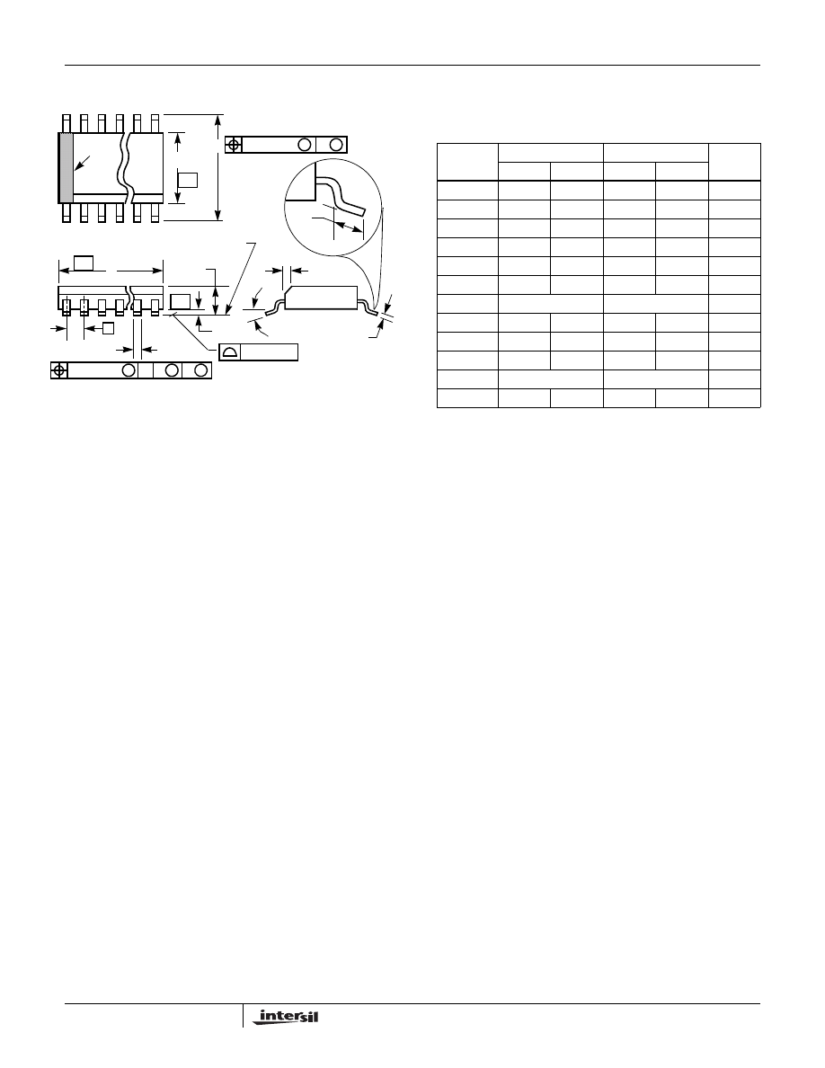
Small Outline Plastic Packages (SOIC)
INDEX
AREA
E
D
N
1
2
3
-B-
0.25(0.010)
C A
M
B S
e
-A-
L
B
M
-C-
A1
A
SEATING PLANE
0.10(0.004)
h x 45°
C
H
0.25(0.010)
B
M
M
α
NOTES:
1. Symbols are defined in the “MO Series Symbol List” in Section 2.2 of
Publication Number 95.
2. Dimensioning and tolerancing per ANSI Y14.5M-1982.
3. Dimension “D” does not include mold flash, protrusions or gate burrs.
Mold flash, protrusion and gate burrs shall not exceed 0.15mm (0.006
inch) per side.
4. Dimension “E” does not include interlead flash or protrusions. Inter-
lead flash and protrusions shall not exceed 0.25mm (0.010 inch) per
side.
5. The chamfer on the body is optional. If it is not present, a visual index
feature must be located within the crosshatched area.
6. “L” is the length of terminal for soldering to a substrate.
7. “N” is the number of terminal positions.
8. Terminal numbers are shown for reference only.
9. The lead width “B”, as measured 0.36mm (0.014 inch) or greater
above the seating plane, shall not exceed a maximum value of
0.61mm (0.024 inch).
10. Controlling dimension: MILLIMETER. Converted inch dimensions
are not necessarily exact.
M8.15
(JEDEC MS-012-AA ISSUE C)
8 LEAD NARROW BODY SMALL OUTLINE PLASTIC PACKAGE
SYMBOL
INCHES
MILLIMETERS
NOTES
MIN
MAX
MIN
MAX
A
0.0532
0.0688
1.35
1.75
-
A1
0.0040
0.0098
0.10
0.25
-
B
0.013
0.020
0.33
0.51
9
C
0.0075
0.0098
0.19
0.25
-
D
0.1890
0.1968
4.80
5.00
3
E
0.1497
0.1574
3.80
4.00
4
e
0.050 BSC
1.27 BSC
-
H
0.2284
0.2440
5.80
6.20
-
h
0.0099
0.0196
0.25
0.50
5
L
0.016
0.050
0.40
1.27
6
N
8
8
7
α
0°
8°
0°
8°
-
Rev. 1 6/05
10
FN2867.9
August 24, 2006
ICM7555, ICM7556
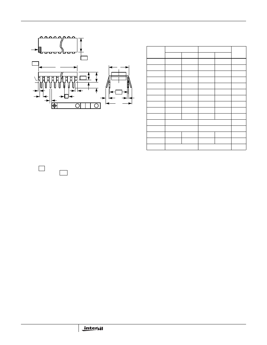
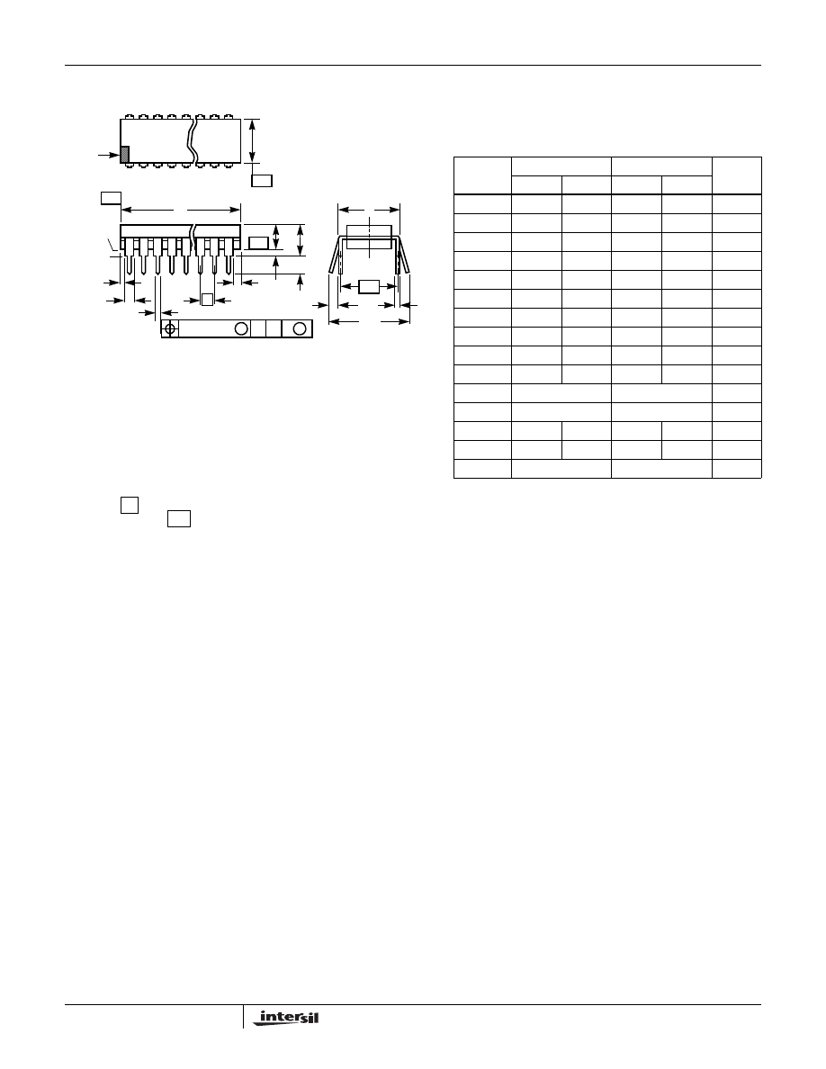
Dual-In-Line Plastic Packages (PDIP)
C
L
E
e
A
C
e
B
e
C
-B-
E1
INDEX
1 2 3
N/2
N
AREA
SEATING
BASE
PLANE
PLANE
-C-
D1
B1
B
e
D
D1
A
A2
L
A
1
-A-
0.010 (0.25)
C
A
M
B S
NOTES:
1. Controlling Dimensions: INCH. In case of conflict between
English and Metric dimensions, the inch dimensions control.
2. Dimensioning and tolerancing per ANSI Y14.5M-1982.
3. Symbols are defined in the “MO Series Symbol List” in Section
2.2 of Publication No. 95.
4. Dimensions A, A1 and L are measured with the package seated
in JEDEC seating plane gauge GS-3.
5. D, D1, and E1 dimensions do not include mold flash or protru-
sions. Mold flash or protrusions shall not exceed 0.010 inch
(0.25mm).
6. E and
are measured with the leads constrained to be per-
pendicular to datum
.
7. e
B
and e
C
are measured at the lead tips with the leads uncon-
strained. e
C
must be zero or greater.
8. B1 maximum dimensions do not include dambar protrusions.
Dambar protrusions shall not exceed 0.010 inch (0.25mm).
9. N is the maximum number of terminal positions.
10. Corner leads (1, N, N/2 and N/2 + 1) for E8.3, E16.3, E18.3,
E28.3, E42.6 will have a B1 dimension of 0.030 - 0.045 inch
(0.76 - 1.14mm).
e
A
-C-
E8.3
(JEDEC MS-001-BA ISSUE D)
8 LEAD DUAL-IN-LINE PLASTIC PACKAGE
SYMBOL
INCHES
MILLIMETERS
NOTES
MIN
MAX
MIN
MAX
A
-
0.210
-
5.33
4
A1
0.015
-
0.39
-
4
A2
0.115
0.195
2.93
4.95
-
B
0.014
0.022
0.356
0.558
-
B1
0.045
0.070
1.15
1.77
8, 10
C
0.008
0.014
0.204
0.355
-
D
0.355
0.400
9.01
10.16
5
D1
0.005
-
0.13
-
5
E
0.300
0.325
7.62
8.25
6
E1
0.240
0.280
6.10
7.11
5
e
0.100 BSC
2.54 BSC
-
e
A
0.300 BSC
7.62 BSC
6
e
B
-
0.430
-
10.92
7
L
0.115
0.150
2.93
3.81
4
N
8
8
9
Rev. 0 12/93
11
FN2867.9
August 24, 2006
ICM7555, ICM7556
Dual-In-Line Plastic Packages (PDIP)
NOTES:
1. Controlling Dimensions: INCH. In case of conflict between English
and Metric dimensions, the inch dimensions control.
2. Dimensioning and tolerancing per ANSI Y14.5M-1982.
3. Symbols are defined in the “MO Series Symbol List” in Section 2.2 of
Publication No. 95.
4. Dimensions A, A1 and L are measured with the package seated in
JEDEC seating plane gauge GS-3.
5. D, D1, and E1 dimensions do not include mold flash or protrusions.
Mold flash or protrusions shall not exceed 0.010 inch (0.25mm).
6. E and
are measured with the leads constrained to be perpen-
dicular to datum
.
7. e
B
and e
C
are measured at the lead tips with the leads uncon-
strained. e
C
must be zero or greater.
8. B1 maximum dimensions do not include dambar protrusions. Dambar
protrusions shall not exceed 0.010 inch (0.25mm).
9. N is the maximum number of terminal positions.
10. Corner leads (1, N, N/2 and N/2 + 1) for E8.3, E16.3, E18.3, E28.3,
E42.6 will have a B1 dimension of 0.030 - 0.045 inch (0.76 -
1.14mm).
e
A
-C-
C
L
E
e
A
C
e
B
e
C
-B-
E1
INDEX
1 2 3
N/2
N
AREA
SEATING
BASE
PLANE
PLANE
-C-
D1
B1
B
e
D
D1
A
A2
L
A1
-A-
0.010 (0.25)
C
A
M
B S
E14.3
(JEDEC MS-001-AA ISSUE D)
14 LEAD DUAL-IN-LINE PLASTIC PACKAGE
SYMBOL
INCHES
MILLIMETERS
NOTES
MIN
MAX
MIN
MAX
A
-
0.210
-
5.33
4
A1
0.015
-
0.39
-
4
A2
0.115
0.195
2.93
4.95
-
B
0.014
0.022
0.356
0.558
-
B1
0.045
0.070
1.15
1.77
8
C
0.008
0.014
0.204
0.355
-
D
0.735
0.775
18.66
19.68
5
D1
0.005
-
0.13
-
5
E
0.300
0.325
7.62
8.25
6
E1
0.240
0.280
6.10
7.11
5
e
0.100 BSC
2.54 BSC
-
e
A
0.300 BSC
7.62 BSC
6
e
B
-
0.430
-
10.92
7
L
0.115
0.150
2.93
3.81
4
N
14
14
9
Rev. 0 12/93
12
All Intersil U.S. products are manufactured, assembled and tested utilizing ISO9000 quality systems.
Intersil Corporation’s quality certifications can be viewed at www.intersil.com/design/quality
Intersil products are sold by description only. Intersil Corporation reserves the right to make changes in circuit design, software and/or specifications at any time without
notice. Accordingly, the reader is cautioned to verify that data sheets are current before placing orders. Information furnished by Intersil is believed to be accurate and
reliable. However, no responsibility is assumed by Intersil or its subsidiaries for its use; nor for any infringements of patents or other rights of third parties which may result
from its use. No license is granted by implication or otherwise under any patent or patent rights of Intersil or its subsidiaries.
For information regarding Intersil Corporation and its products, see www.intersil.com
FN2867.9
August 24, 2006
ICM7555, ICM7556
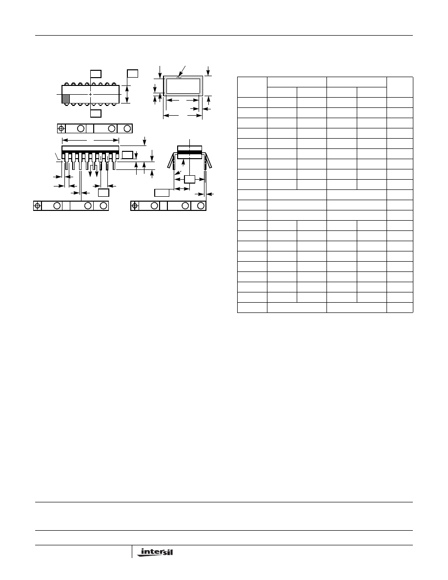
Ceramic Dual-In-Line Frit Seal Packages (CERDIP)
NOTES:
1. Index area: A notch or a pin one identification mark shall be locat-
ed adjacent to pin one and shall be located within the shaded
area shown. The manufacturer’s identification shall not be used
as a pin one identification mark.
2. The maximum limits of lead dimensions b and c or M shall be
measured at the centroid of the finished lead surfaces, when
solder dip or tin plate lead finish is applied.
3. Dimensions b1 and c1 apply to lead base metal only. Dimension
M applies to lead plating and finish thickness.
4. Corner leads (1, N, N/2, and N/2+1) may be configured with a
partial lead paddle. For this configuration dimension b3 replaces
dimension b2.
5. This dimension allows for off-center lid, meniscus, and glass
overrun.
6. Dimension Q shall be measured from the seating plane to the
base plane.
7. Measure dimension S1 at all four corners.
8. N is the maximum number of terminal positions.
9. Dimensioning and tolerancing per ANSI Y14.5M - 1982.
10. Controlling dimension: INCH.
bbb
C A - B
S
c
Q
L
A
SEATING
BASE
D
PLANE
PLANE
-D-
-A-
-C-
-B-
α
D
E
S1
b2
b
A
e
M
c1
b1
(c)
(b)
SECTION A-A
BASE
LEAD FINISH
METAL
e
A/2
A
M
S
S
ccc
C A - B
M
D
S
S
aaa
C A - B
M
D
S
S
e
A
F14.3
MIL-STD-1835 GDIP1-T14 (D-1, CONFIGURATION A)
14 LEAD CERAMIC DUAL-IN-LINE FRIT SEAL PACKAGE
SYMBOL
INCHES
MILLIMETERS
NOTES
MIN
MAX
MIN
MAX
A
-
0.200
-
5.08
-
b
0.014
0.026
0.36
0.66
2
b1
0.014
0.023
0.36
0.58
3
b2
0.045
0.065
1.14
1.65
-
b3
0.023
0.045
0.58
1.14
4
c
0.008
0.018
0.20
0.46
2
c1
0.008
0.015
0.20
0.38
3
D
-
0.785
-
19.94
5
E
0.220
0.310
5.59
7.87
5
e
0.100 BSC
2.54 BSC
-
eA
0.300 BSC
7.62 BSC
-
eA/2
0.150 BSC
3.81 BSC
-
L
0.125
0.200
3.18
5.08
-
Q
0.015
0.060
0.38
1.52
6
S1
0.005
-
0.13
-
7
α
90°
105°
90°
105°
-
aaa
-
0.015
-
0.38
-
bbb
-
0.030
-
0.76
-
ccc
-
0.010
-
0.25
-
M
-
0.0015
-
0.038
2, 3
N
14
14
8
Rev. 0 4/94
Wyszukiwarka
Podobne podstrony:
intersekcja geologiczna
Programowanie Interstarid 13046
7556
Pierwotna i wtórna intersubiektywność wykłąd 5
Intersubiektywny kontekst doświadczenia ciała w fenomenologi Husserla
ICM7555 Philips
7556
1---PAGO-osw.-chł.-baza, 1---Eksporty-all, 1---Eksporty---, 12---agencje-celne, 1---A.C.-Intersped-B
praca zaliczeniowa ze wstymulacji aktywności werbalnej w pracy przedszkola metoda intersemiotyczna
Analiza otoczenia firmy Interspeed sp. z o.o., strategia
PODSTAWOWE WIADOMOŚCI Z INTERSEKCJI GEOLOGICZNEJ
POETYKA INTERSEMIOTYCZNA
7556
PRZEKŁAD INTERSEMIOTYCZNY, Pedagogika, Edukacja wczesnoszkolna - polski
PRZEKŁAD INTERSEMIOTYCZNY W KSZTAŁCENIU LITERACKIM
metoda przekładu intersemiotycznego dyduchowa
więcej podobnych podstron