2SC460, 2SC461
Silicon NPN Epitaxial Planar
Application
•
2SC460 high frequency amplifier, mixer
•
2SC461 VHF amplifier, mixer
Outline
1. Emitter
2. Collector
3. Base
TO-92 (2)
3
2
1
2SC460, 2SC461
2
Absolute Maximum Ratings (Ta = 25°C)
Item
Symbol
2SC460
2SC461
Unit
Collector to base voltage
V
CBO
30
30
V
Collector to emitter voltage
V
CEO
30
30
V
Emitter to base voltage
V
EBO
5
5
V
Collector current
I
C
100
100
mA
Collector power dissipation
P
C
200
200
mW
Junction temperature
Tj
150
150
°
C
Storage temperature
Tstg
–55 to +150
–55 to +150
°
C

2SC460, 2SC461
3
Electrical Characteristics (Ta = 25°C)
2SC460
2SC461
Item
Symbol
Min
Typ
Max
Min
Typ
Max
Unit
Test conditions
Collector to base
breakdown voltage
V
(BR)CBO
30
—
—
30
—
—
V
I
C
= 10
µ
A, I
E
= 0
Collector to emitter
breakdown voltage
V
(BR)CEO
30
—
—
30
—
—
V
I
C
= 1 mA, R
BE
=
∞
Emitter to base
breakdown voltage
V
(BR)EBO
5
—
—
5
—
—
V
I
E
= 10
µ
A, I
C
= 0
Collector cutoff current
I
CBO
—
—
0.5
—
—
0.5
µ
A
V
CB
= 18 V, I
E
= 0
Emitter cutoff current
I
EBO
—
—
0.5
—
—
0.5
µ
A
V
EB
= 2 V, I
C
= 0
Base to emitter voltage
V
BE
—
0.63
0.75
—
0.63
0.75
V
V
CE
= 12 V, I
C
= 2 mA
DC current transfer ratio h
FE
*
1
35
—
200
35
—
200
V
CE
= 12 V, I
C
= 2 mA
Collector to emitter
saturation voltage
V
CE(sat)
—
0.6
1.1
—
0.6
1.1
V
I
C
= 10 mA, I
B
= 1 mA
Gain bandwidth product f
T
—
230
—
—
230
—
MHz
V
CE
= 12 V, I
C
= 2 mA
Collector output
capacitance
C
ob
—
1.8
3.5
—
1.8
3.5
pF
V
CB
= 10 V, I
E
= 0,
f = 1 MHz
10.7 MHz power gain
PG
26
29
—
—
—
—
dB
V
CE
= 6 V, I
E
= –1 mA
f = 10.7 MHz
100 MHz power gain
PG
—
—
—
13
17
—
dB
V
CE
= 6 V, I
E
= –1 mA
f = 100 MHz
Noise figure
NF
—
2.0
—
—
—
—
dB
V
CE
= 6 V, I
E
= –1 mA
f = 1MHz
R
g
= 500
Ω
Note:
1. The 2SC460 and 2SC461 are grouped by h
FE
as follows.
A
B
C
35 to 70
60 to 120
100 to 200
2SC460, 2SC461
4
Small Signal y Parameters (V
CE
= 6 V, I
C
= 1 mA, Emitter Common)
Item
Symbol f
2SC460A,
2S461A
2SC460B,
2SC461B
2SC460C,
2SC461C
Unit
Input admittance
yie
455 kHz
0.58 + j0.074
0.42 + j0.068
0.30 + j0.051
mS
4.5 MHz
0.65 + j0.79
0.50 + j0.7
0.35 + j0.57
10.7 MHz 0.91 + j2.0
0.61 + j1.9
0.39 + j1.3
100 MHz 7.4 + j14
5.6 + j12
3.8 + j6.0
Reverse transfer admittance yre
455 kHz
–j0.003
–j0.003
–j0.003
mS
4.5 MHz
–j0.04
–j0.04
–j0.04
10.7 MHz –j0.13
–j0.13
–j0.13
100 MHz –j1.0
–j1.0
–j1.0
Forward transfer admittance yfe
455 kHz
38 – j0.1
37 – j0.1
37 – j0.2
mS
4.5 MHz
35 – j1.0
35 – j1.2
34 – j1.8
10.7 MHz 34 – j2.5
34 – j2.5
33 – j4.5
100 MHz 28 – j20
28 – j19
20 – j19
Output admittance
yoe
455 kHz
0.0098 + j0.009 0.013 + j0.009
0.016 + j0.012
mS
4.5 MHz
0.02 + j0.09
0.023 + j0.092
0.03 + j0.10
10.7 MHz 0.11 + j0.4
0.11 + j0.4
0.12 + j0.4
100 MHz 0.40 + j1.7
0.50 + j2.0
0.83 + j2.0
2SC460, 2SC461
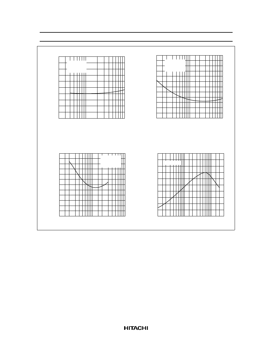
5
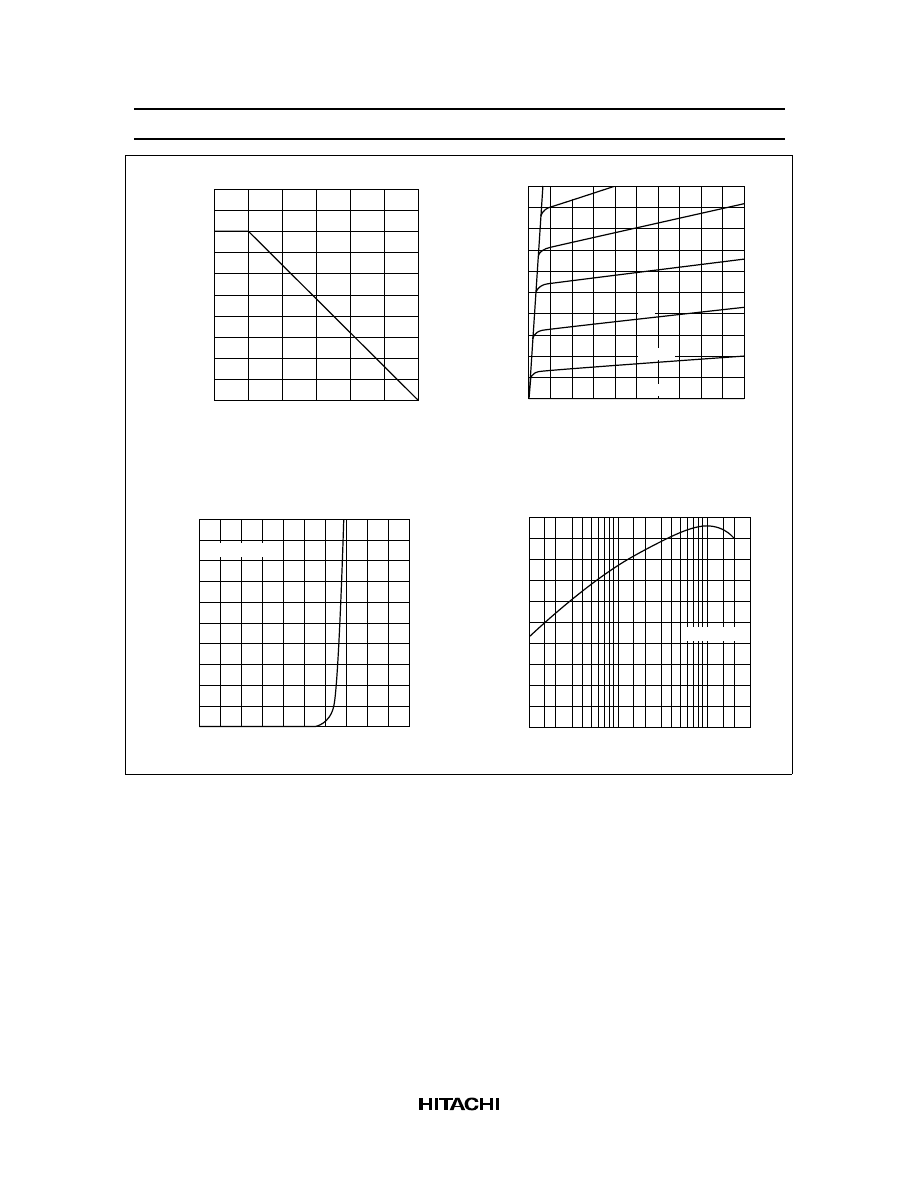
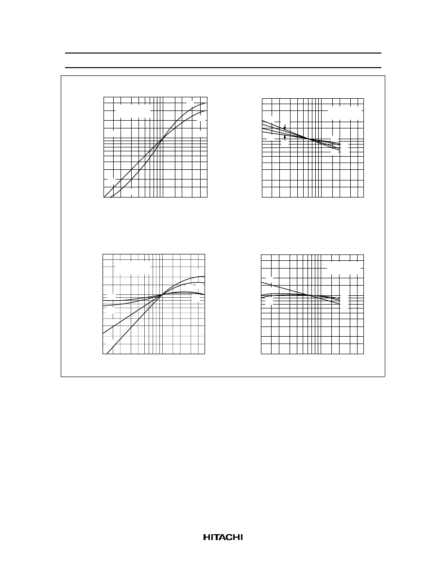
0
50
150
100
250
200
50
Ambient Temperature Ta (
°
C)
Collector Power Dissipation P
C
(mW)
Maximum Collector Dissipation Curve
100
150
0
2
6
4
10
8
8
4
Collector to Emitter Voltage V
CE
(V)
Collector Current I
C
(mA)
Typical Output Characteristics
12
16
20
20
µ
A
40
60
80
100
I
B
= 0
0
2
6
4
10
8
0.4
0.2
Base to Emitter Voltage V
BE
(V)
Collector Current I
C
(mA)
Typical Transfer Characteristics
0.6
0.8
1.0
V
CE
= 6 V
0
20
60
40
100
80
1.0
0.3
0.1
Collector Current I
C
(mA)
DC Current Transfer Ratio h
FE
DC Current Transfer Ratio vs.
Collector Current
3
10
30
V
CE
= 6 V
2SC460, 2SC461
6
0
1
3
2
5
4
1.0
0.5
0.2
Collector Current I
C
(mA)
Noise Figure NF (dB)
Noise Figure vs. Collector Current
2
5
10
V
CE
= 6 V
R
g
= 500
Ω
f = 1.0 MHz
0
4
16
12
8
24
20
1.0
0.5
0.2
0.1
Collector Current I
C
(mA)
Noise Figure NF (dB)
Noise Figure vs. Collector Current
2
5
10
V
CE
= 6 V
R
g
= 50
Ω
f = 100 MHz
0
2
8
6
4
12
10
100
50
10
20
Signal Source Resistance R
g
(
Ω
)
Noise Figure NF (dB)
Noise Figure vs. Signal Source Resistance
200
500 1000
V
CE
= 6 V
I
C
= 1 mA
f = 100 MHz
0
100
300
200
500
400
1.0
0.3
0.1
Collector Current I
C
(mA)
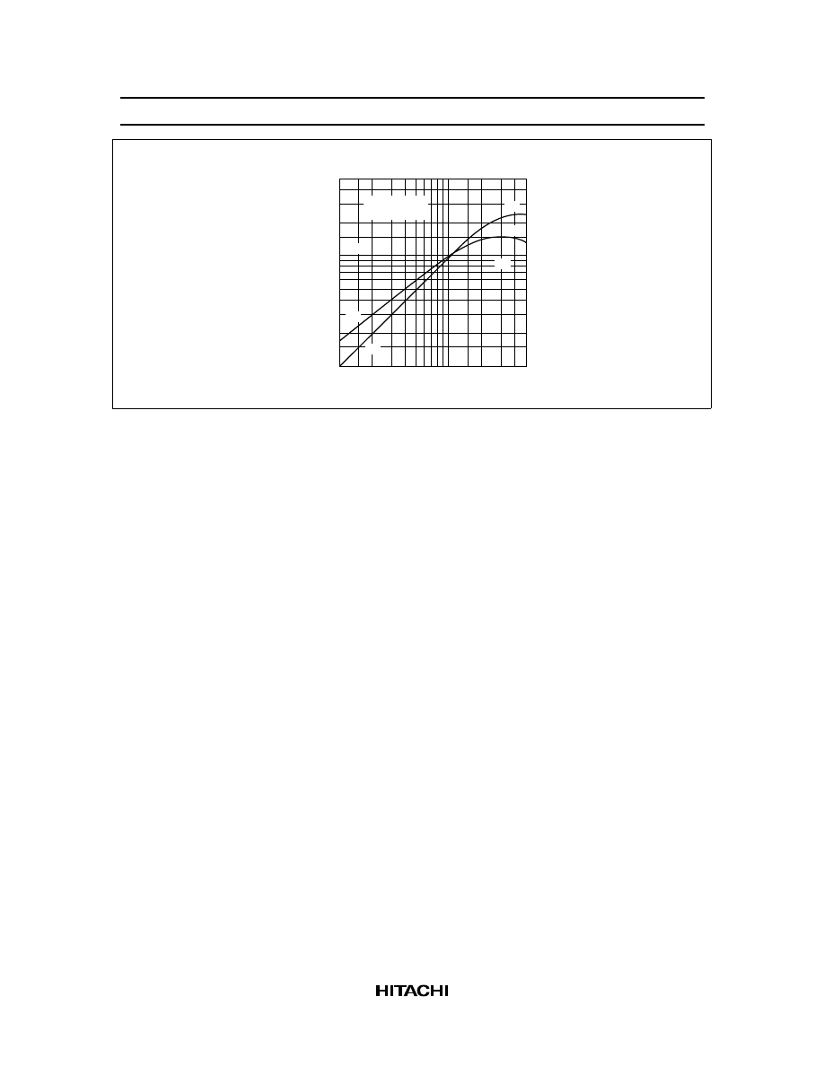
Gain Bandwidth Product f
T
(MHz)
Gain Bandwidth Product vs.
Collector Current
3
10
30
V
CE
= 6 V
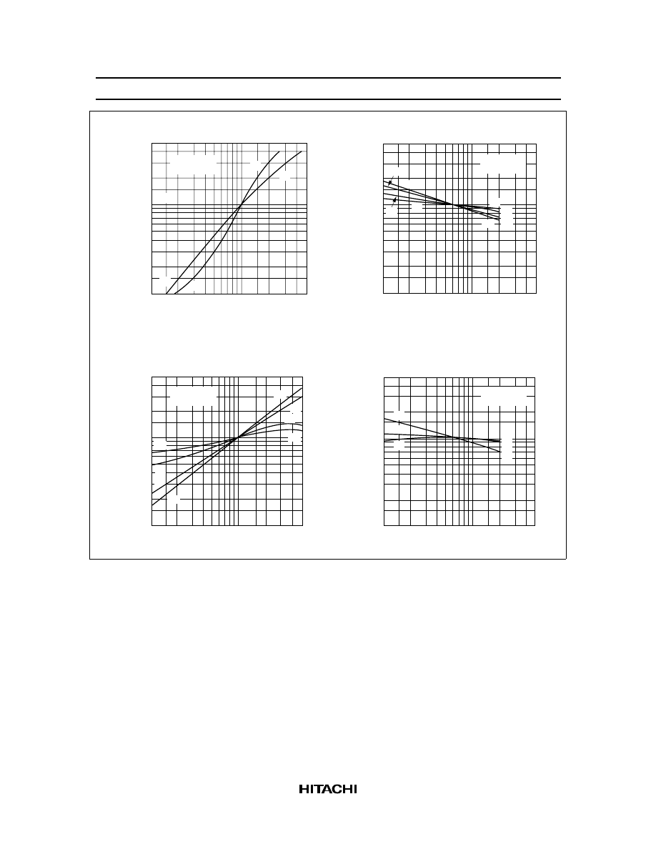
2SC460, 2SC461
7
0
100
300
200
400
5
2
1
Collector to Emitter Volgage V
CE
(V)
Gain Bandwidth Product f
T
(MHz)
Gain Bandwidth Product vs.
Collector to Emitter Voltage
10
20
I
C
= 1 mA
10
20
200
100
50
500
5
2
1
Collector to Emitter Voltage V
CE
(V)
Percentage of Relative to V
CE
= 6 V (%)
Input/Output Admittance vs.
Collector to Emitter Voltage
20
10
50
I
C
= 1 mA
f = 455 kHz
g
ie
g
ie
g
oe
g
oe
b
oe
b
oe
b
ie
b
ie
10
20
200
100
50
500
0.5
0.2
0.1
Collector Current I
C
(mA)
Percentage of Relative to I
E
= 1 mA (%)
Input/Output Admittance vs.
Collector Current
2
1.0
5
V
CE
= 6 V
f = 455 kHz
g
ie
g
ie
b
ie
b
ie
g
oe
g
oe
b
oe
b
oe
10
20
200
100
50
500
5
2
1
Collector to Emitter Voltage V
CE
(V)
Percentage of Relative to V
CE
= 6 V (%)
Transfer Admittance vs.
Collector to Emitter Voltage
20
10
50
I
C
= 1 mA
f = 455 kHz
b
re
b
re
b
fe
b
fe
g
fe
g
fe
2SC460, 2SC461
8
10
20
200
100
50
500
0.5
0.2
0.1
Collector Current I
C
(mA)
Percentage of Relative to I
C
= 1 mA (%)
Transfer Admittance vs.
Collector Current
2
1.0
5
V
CE
= 6 V
f = 455 kHz
b
re
b
re
b
fe
b
fe
g
fe
g
fe
10
20
200
100
50
500
5
2
1
Collector to Emitter Voltage V
CE
(V)
Percentage of Relative to V
CE
= 6 V (%)
Input/Output Admittance vs.
Collector to Emitter Voltage
20
10
50
I
C
= 1 mA
f = 4.5 MHz
g
ie
g
ie
g
oe
g
oe
b
oe
b
oe
b
ie
b
ie
10
20
200
100
50
500
0.5
0.2
0.1
Collector Current I
C
(mA)
Percentage of Relative to I
C
= 1 mA (%)
Input/Output Admittance vs.
Collector Current
2
1.0
5
V
CE
= 6 V
f = 4.5 MHz
g
ie
g
ie
b
ie
b
ie
g
oe
g
oe
b
oe
b
oe
10
20
200
100
50
500
5
2
1
Collector to Emitter Voltage V
CE
(V)
Percentage of Relative to V
CE
= 6 V (%)
Transfer Admittance vs.
Collector to Emitter Voltage
20
10
50
I
C
= 1 mA
f = 4.5 MHz
b
re
b
fe
g
fe
b
re
b
fe
g
fe
2SC460, 2SC461
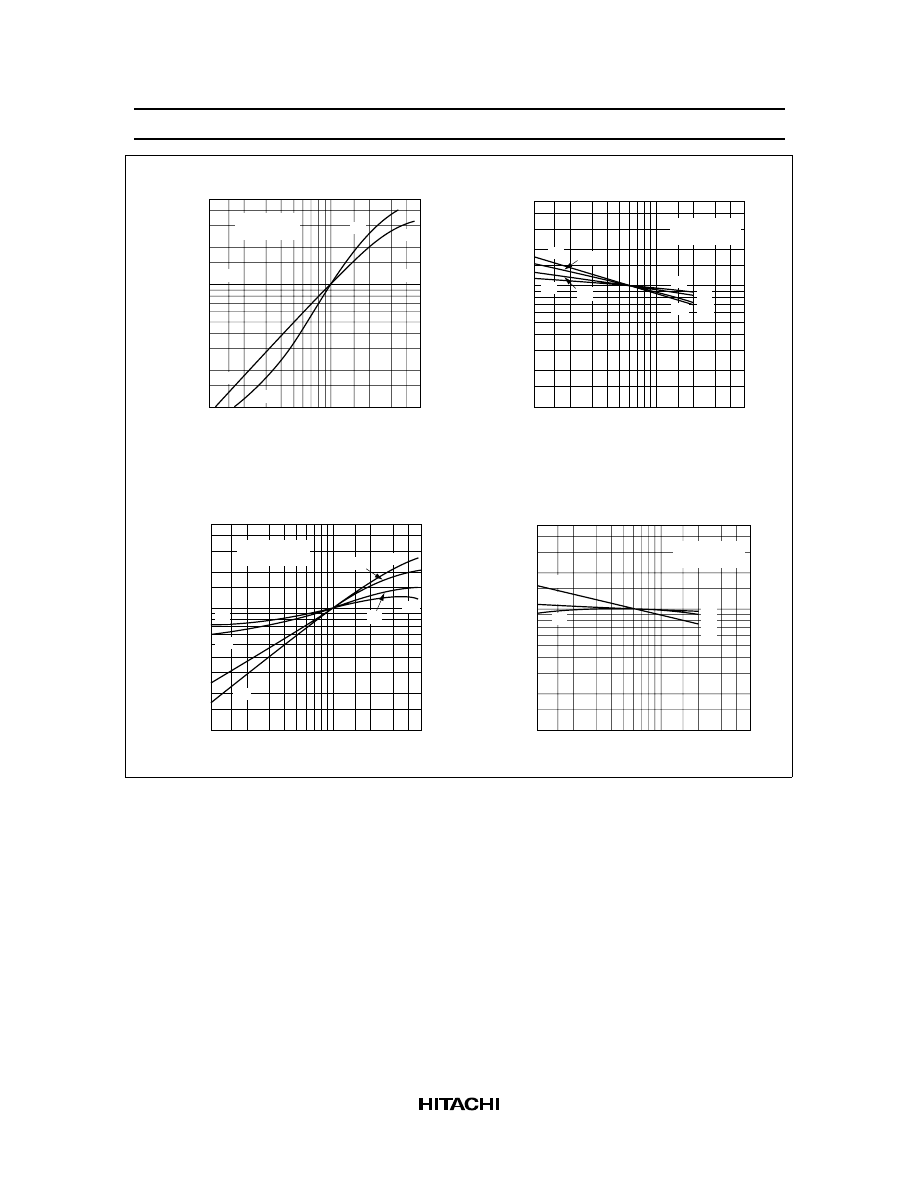
9
10
20
200
100
50
500
0.5
0.2
0.1
Collector Current I
C
(mA)
Percentage of Relative to I
C
= 1 mA (%)
Transfer Admittance vs.
Collector Current
2
1.0
5
V
CE
= 6 V
f = 4.5 MHz
b
fe
b
fe
g
fe
g
fe
b
re
b
re
10
20
200
100
50
500
5
2
1
Collector to Emitter Voltage V
CE
(V)
Percentage of Relative to V
CE
= 6 V (%)
Input/Output Admittance vs.
Collector to Emitter Voltage
20
10
50
I
C
= 1 mA
f = 10.7 MHz
b
oe
b
oe
b
ie
b
ie
g
ie
g
ie
g
oe
g
oe
10
20
200
100
50
500
0.5
0.2
0.1
Collector Current I
C
(mA)
Percentage of Relative to I
C
= 1 mA (%)
Input/Output Admittance vs.
Collector Current
2
1.0
5
V
CE
= 6 V
f = 10.7 MHz
g
ie
g
ie
b
ie
b
ie
g
oe
g
oe
b
oe
b
oe
10
20
200
100
50
500
5
2
1
Collector to Emitter Voltage V
CE
(V)
Percentage of Relative to V
CE
= 6 V (%)
Transfer Admittance vs.
Collector to Emitter Voltage
20
10
50
I
C
= 1 mA
f = 10.7 MHz
g
ie
g
ie
b
fe
b
fe
b
re
b
re
2SC460, 2SC461
10
10
20
200
100
50
500
0.5
0.2
0.1
Collector Current I
C
(mA)
Percentage of Relative to I
C
= 1 mA (%)
Transfer Admittance vs.
Collector Current
2
1.0
5
V
CE
= 6 V
f = 10.7 MHz
b
fe
b
fe
g
fe
g
fe
b
re
b
re
10
20
200
100
50
500
5
2
1
Collector to Emitter Voltage V
CE
(V)
Percentage of Relative to V
CE
= 6 V (%)
Input/Output Admittance vs.
Collector to Emitter Voltage
20
10
50
I
C
= 1 mA
f = 100 MHz
g
ie
g
ie
g
oe
g
oe
b
ie
b
ie
b
oe
b
oe
10
20
200
100
50
500
0.5
0.2
0.1
Collector Current I
C
(mA)
Percentage of Relative to I
C
= 1 mA (%)
Input/Output Admittance vs.
Collector Current
2
1.0
5
V
CE
= 6 V
f = 100 MHz
b
oe
b
oe
b
ie
b
ie
g
ie
g
ie
g
oe
g
oe
10
20
200
100
50
500
5
2
1
Collector to Emitter Voltage V
CE
(V)
Percentage of Relative to V
CE
= 6 V (%)
Transfer Admittance vs.
Collector to Emitter Voltage
20
10
50
I
C
= 1 mA
f = 100 MHz
b
fe
b
fe
b
re
b
re
g
fe
g
fe
2SC460, 2SC461
11
10
20
200
100
50
500
0.5
0.2
0.1
Collector Current I
C
(mA)
Percentage of Relative to I
C
= 1 mA (%)
Transfer Admittance vs.
Collector Current
2
1.0
5
V
CE
= 6 V
f = 100 MHz
b
re
b
re
b
fe
b
fe
g
fe
g
fe
0.60 Max
0.45
±
0.1
4.8
±
0.3
3.8
±
0.3
5.0
±
0.2
0.7
2.3 Max
12.7 Min
0.5
1.27
2.54
Hitachi Code
JEDEC
EIAJ
Weight (reference value)
TO-92 (2)
Conforms
Conforms
0.25 g
Unit: mm
Cautions
1. Hitachi neither warrants nor grants licenses of any rights of Hitachi’s or any third party’s patent,
copyright, trademark, or other intellectual property rights for information contained in this document.
Hitachi bears no responsibility for problems that may arise with third party’s rights, including
intellectual property rights, in connection with use of the information contained in this document.
2. Products and product specifications may be subject to change without notice. Confirm that you have
received the latest product standards or specifications before final design, purchase or use.
3. Hitachi makes every attempt to ensure that its products are of high quality and reliability. However,
contact Hitachi’s sales office before using the product in an application that demands especially high
quality and reliability or where its failure or malfunction may directly threaten human life or cause risk
of bodily injury, such as aerospace, aeronautics, nuclear power, combustion control, transportation,
traffic, safety equipment or medical equipment for life support.
4. Design your application so that the product is used within the ranges guaranteed by Hitachi particularly
for maximum rating, operating supply voltage range, heat radiation characteristics, installation
conditions and other characteristics. Hitachi bears no responsibility for failure or damage when used
beyond the guaranteed ranges. Even within the guaranteed ranges, consider normally foreseeable
failure rates or failure modes in semiconductor devices and employ systemic measures such as fail-
safes, so that the equipment incorporating Hitachi product does not cause bodily injury, fire or other
consequential damage due to operation of the Hitachi product.
5. This product is not designed to be radiation resistant.
6. No one is permitted to reproduce or duplicate, in any form, the whole or part of this document without
written approval from Hitachi.
7. Contact Hitachi’s sales office for any questions regarding this document or Hitachi semiconductor
products.
Hitachi, Ltd.
Semiconductor & Integrated Circuits.
Nippon Bldg., 2-6-2, Ohte-machi, Chiyoda-ku, Tokyo 100-0004, Japan
Tel: Tokyo (03) 3270-2111 Fax: (03) 3270-5109
Copyright ' Hitachi, Ltd., 1999. All rights reserved. Printed in Japan.
Hitachi Asia Pte. Ltd.
16 Collyer Quay #20-00
Hitachi Tower
Singapore 049318
Tel: 535-2100
Fax: 535-1533
URL
NorthAmerica
: http:semiconductor.hitachi.com/
Europe
: http://www.hitachi-eu.com/hel/ecg
Asia (Singapore)
: http://www.has.hitachi.com.sg/grp3/sicd/index.htm
Asia (Taiwan)
: http://www.hitachi.com.tw/E/Product/SICD_Frame.htm
Asia (HongKong)
: http://www.hitachi.com.hk/eng/bo/grp3/index.htm
Japan
: http://www.hitachi.co.jp/Sicd/indx.htm
Hitachi Asia Ltd.
Taipei Branch Office
3F, Hung Kuo Building. No.167,
Tun-Hwa North Road, Taipei (105)
Tel: <886> (2) 2718-3666
Fax: <886> (2) 2718-8180
Hitachi Asia (Hong Kong) Ltd.
Group III (Electronic Components)
7/F., North Tower, World Finance Centre,
Harbour City, Canton Road, Tsim Sha Tsui,
Kowloon, Hong Kong
Tel: <852> (2) 735 9218
Fax: <852> (2) 730 0281
Telex: 40815 HITEC HX
Hitachi Europe Ltd.
Electronic Components Group.
Whitebrook Park
Lower Cookham Road
Maidenhead
Berkshire SL6 8YA, United Kingdom
Tel: <44> (1628) 585000
Fax: <44> (1628) 778322
Hitachi Europe GmbH
Electronic components Group
Dornacher Stra§e 3
D-85622 Feldkirchen, Munich
Germany
Tel: <49> (89) 9 9180-0
Fax: <49> (89) 9 29 30 00
Hitachi Semiconductor
(America) Inc.
179 East Tasman Drive,
San Jose,CA 95134
Tel: <1> (408) 433-1990
Fax: <1>(408) 433-0223
For further information write to:
Wyszukiwarka
Podobne podstrony:
460 461
2SC 945
2SC 828 2SC 828A
2SC 945
ST 2SC 945
2SC 535 [R]
2SC 535 [H]
460 461
Dz U 09 56 461 Warunki Techniczne zmiany
091 zmiana Dz U 2012 460
GS 300 460, od 01 2005
460
460
460-470, materiały ŚUM, IV rok, Patomorfologia, egzamin, opracowanie 700 pytan na ustny
460
Zobowiązania, ART 461 KC, 1990
460
461
więcej podobnych podstron