4-5
CAUTION: These devices are sensitive to electrostatic discharge; follow proper ESD Handling Procedures.
http://www.intersil.com or 407-727-9207
|
Copyright
©
Intersil Corporation 1999
BUZ11
30A, 50V, 0.040 Ohm, N-Channel Power
MOSFET
This is an N-Channel enhancement mode silicon gate power
field effect transistor designed for applications such as
switching regulators, switching converters, motor drivers,
relay drivers and drivers for high power bipolar switching
transistors requiring high speed and low gate drive power.
This type can be operated directly from integrated circuits.
Formerly developmental type TA9771.
Features
• 30A, 50V
• r
DS(ON)
= 0.040
Ω
• SOA is Power Dissipation Limited
• Nanosecond Switching Speeds
• Linear Transfer Characteristics
• High Input Impedance
• Majority Carrier Device
• Related Literature
- TB334 “Guidelines for Soldering Surface Mount
Components to PC Boards”
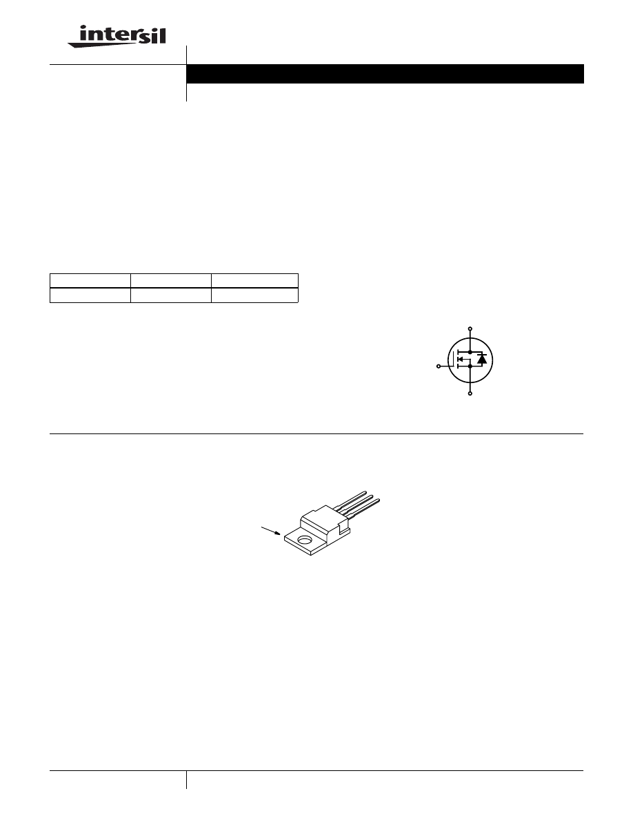
Symbol
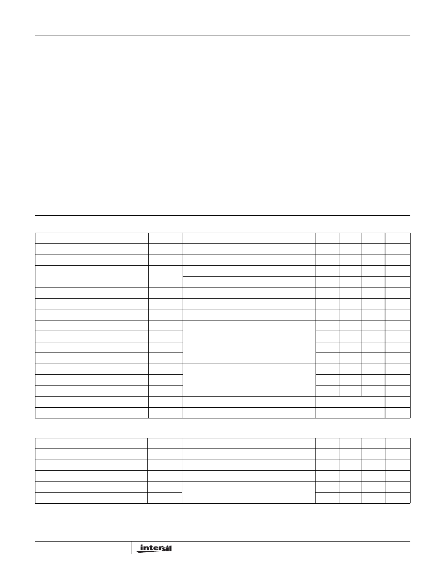
Packaging
JEDEC TO-220AB
Ordering Information
PART NUMBER
PACKAGE
BRAND
BUZ11
TO-220AB
BUZ11
NOTE: When ordering, use the entire part number.
G
D
S
GATE
DRAIN (FLANGE)
SOURCE
DRAIN
June 1999
File Number
2253.2
Data Sheet
4-6
Absolute Maximum Ratings
T
C
= 25
o
C, Unless Otherwise Specified
BUZ11
UNITS
Drain to Source Breakdown Voltage (Note 1) . . . . . . . . . . . . . . . . . . . . . . . . . . . . . . . . . . . . . . .V
DS
50
V
Drain to Gate Voltage (R
GS
= 20k
Ω
) (Note 1) . . . . . . . . . . . . . . . . . . . . . . . . . . . . . . . . . . . . . V
DGR
50
V
Continuous Drain Current
T
C
= 30
o
C. . . . . . . . . . . . . . . . . . . . . . . . . . . . . . . . . . . . . . . . . . . . . I
D
30
A
Pulsed Drain Current (Note 3) . . . . . . . . . . . . . . . . . . . . . . . . . . . . . . . . . . . . . . . . . . . . . . . . . . . I
DM
120
A
Gate to Source Voltage . . . . . . . . . . . . . . . . . . . . . . . . . . . . . . . . . . . . . . . . . . . . . . . . . . . . . . . .V
GS
±
20
V
Maximum Power Dissipation . . . . . . . . . . . . . . . . . . . . . . . . . . . . . . . . . . . . . . . . . . . . . . . . . . . . .P
D
75
W
Linear Derating Factor . . . . . . . . . . . . . . . . . . . . . . . . . . . . . . . . . . . . . . . . . . . . . . . . . . . . . . . . . . . .
0.6
W/
o
C
Operating and Storage Temperature . . . . . . . . . . . . . . . . . . . . . . . . . . . . . . . . . . . . . . . . . . T
J,
T
STG
-55 to 150
o
C
DIN Humidity Category - DIN 40040 . . . . . . . . . . . . . . . . . . . . . . . . . . . . . . . . . . . . . . . . . . . . . . . . .
E
IEC Climatic Category - DIN IEC 68-1 . . . . . . . . . . . . . . . . . . . . . . . . . . . . . . . . . . . . . . . . . . . . . . . .
55/150/56
Maximum Temperature for Soldering
Leads at 0.063in (1.6mm) from Case for 10s . . . . . . . . . . . . . . . . . . . . . . . . . . . . . . . . . . . . . . . T
L
Package Body for 10s, See Techbrief 334 . . . . . . . . . . . . . . . . . . . . . . . . . . . . . . . . . . . . . . . T
pkg
300
260
o
C
o
C
CAUTION: Stresses above those listed in “Absolute Maximum Ratings” may cause permanent damage to the device. This is a stress only rating and operation of the
device at these or any other conditions above those indicated in the operational sections of this specification is not implied.
NOTE:
1. T
J
= 25
o
C to 125
o
C.
Electrical Specifications
T
C
= 25
o
C, Unless Otherwise Specified
PARAMETER
SYMBOL
TEST CONDITIONS
MIN
TYP
MAX
UNITS
Drain to Source Breakdown Voltage
BV
DSS
I
D
= 250
µ
A, V
GS
= 0V
50
-
-
V
Gate Threshold Voltage
V
GS(TH)
V
GS
= V
DS
, I
D
= 1mA (Figure 9)
2.1
3
4
V
Zero Gate Voltage Drain Current
I
DSS
T
J
= 25
o
C, V
DS
= 50V, V
GS
= 0V
-
20
250
µ
A
T
J
= 125
o
C, V
DS
= 50V, V
GS
= 0V
-
100
1000
µ
A
Gate to Source Leakage Current
I
GSS
V
GS
= 20V, V
DS
= 0V
-
10
100
nA
Drain to Source On Resistance (Note 2)
r
DS(ON)
I
D
= 15A, V
GS
= 10V (Figure 8)
-
0.03
0.04
Ω
Forward Transconductance (Note 2)
gfs
V
DS
= 25V, I
D
= 15A (Figure 11)
4
8
-
S
Turn-On Delay Time
t
d(ON)
V
CC
= 30V, I
D
≈
3A, V
GS
= 10V, R
GS
= 50
Ω,
R
L
= 10
Ω
-
30
45
ns
Rise Time
t
r
-
70
110
ns
Turn-Off Delay Time
t
d(OFF)
-
180
230
ns
Fall Time
t
f
-
130
170
ns
Input Capacitance
C
ISS
V
DS
= 25V, V
GS
= 0V, f = 1MHz (Figure 10)
-
1500
2000
pF
Output Capacitance
C
OSS
-
750
1100
pF
Reverse Transfer Capacitance
C
RSS
-
250
400
pF
Thermal Resistance Junction to Case
R
θ
JC
≤
1.67
o
C/W
Thermal Resistance Junction to Ambient
R
θ
JA
≤
75
o
C/W
Source to Drain Diode Specifications
PARAMETER
SYMBOL
TEST CONDITIONS
MIN
TYP
MAX
UNITS
Continuous Source to Drain Current
I
SD
T
C
= 25
o
C
-
-
30
A
Pulsed Source to Drain Current
I
SDM
T
C
= 25
o
C
-
-
120
A
Source to Drain Diode Voltage
V
SD
T
J
= 25
o
C, I
SD
= 60A, V
GS
= 0V
-
1.7
2.6
V
Reverse Recovery Time
t
rr
T
J
= 25
o
C, I
SD
= 30A, dI
SD
/dt = 100A/
µ
s,
V
R
= 30V
-
200
-
ns
Reverse Recovery Charge
Q
RR
-
0.25
-
µ
C
NOTES:
2. Pulse Test: Pulse width
≤
300ms, duty cycle
≤
2%.
3. Repetitive rating: pulse width limited by maximum junction temperature. See Transient Thermal Impedance curve (Figure 3).
BUZ11
4-7
Typical Performance Curves
Unless Otherwise Specified
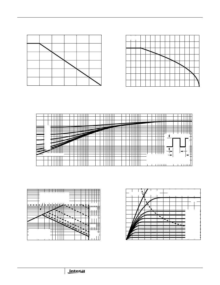
FIGURE 1. NORMALIZED POWER DISSIPATION vs CASE
TEMPERATURE
FIGURE 2. MAXIMUM CONTINUOUS DRAIN CURRENT vs
CASE TEMPERATURE
FIGURE 3. MAXIMUM TRANSIENT THERMAL IMPEDANCE
FIGURE 4. FORWARD BIAS SAFE OPERATING AREA
FIGURE 5. OUTPUT CHARACTERISTICS
T
A
, CASE TEMPERATURE (
o
C)
PO
WER DISSIP
A
TION MUL
TIPLIER
0
0
25
50
75
100
150
0.2
0.4
0.6
0.8
1.0
1.2
125
40
30
20
10
0
0
50
100
150
T
C
, CASE TEMPERATURE (
o
C)
I
D
, DRAIN CURRENT (A)
V
GS
> 10V
10
-5
10
-4
10
-3
10
-2
10
-1
10
0
10
1
t, RECTANGULAR PULSE DURATION (s)
Z
θ
JC,
TRANSIENT THERMAL IMPED
ANCE
1
0.1
0.01
SINGLE PULSE
0.5
0.2
0.1
0.05
0.02
0.01
P
DM
NOTES:
DUTY FACTOR: D = t
1
/t
2
PEAK T
J
= P
DM
x Z
θ
JC
+ T
C
t
1
t
2
V
DS
, DRAIN TO SOURCE VOLTAGE (V)
I
D
, DRAIN CURRENT (A)
100
µ
s
10
µ
s
DC
1ms
10ms
100ms
10
3
10
2
10
1
10
0
10
0
10
1
10
2
2.5
µ
s
OPERATION IN THIS
AREA MAY BE LIMITED
BY r
DS(ON)
T
C
= 25
o
C
T
J
= MAX RATED
SINGLE PULSE
60
50
40
30
20
10
0
I
D
, DRAIN CURRENT (A)
0
1
2
3
4
5
6
V
DS
, DRAIN TO SOURCE VOLTAGE (V)
V
GS
= 8.0V
V
GS
= 7.5V
V
GS
= 7.0V
V
GS
= 6.5V
V
GS
= 6.0V
V
GS
= 5.5V
V
GS
= 5.0V
V
GS
= 4.5V
V
GS
= 4.0V
10V
V
GS
= 20V
PULSE DURATION = 80
µ
s
P
D
= 75W
DUTY CYCLE = 0.5% MAX
BUZ11
4-8
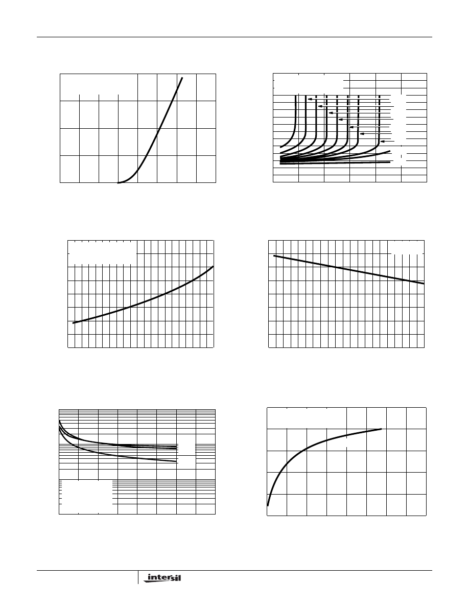
FIGURE 6. TRANSFER CHARACTERISTICS
FIGURE 7. DRAIN TO SOURCE ON RESISTANCE vs GATE
VOLTAGE AND DRAIN CURRENT
FIGURE 8. DRAIN TO SOURCE ON RESISTANCE vs
JUNCTION TEMPERATURE
FIGURE 9. GATE THRESHOLD VOLTAGE vs JUNCTION
TEMPERATURE
FIGURE 10. CAPACITANCE vs DRAIN TO SOURCE VOLTAGE
FIGURE 11. TRANSCONDUCTANCE vs DRAIN CURRENT
Typical Performance Curves
Unless Otherwise Specified (Continued)
20
15
10
5
0
I
DS(ON),
DRAIN T
O
SOURCE CURRENT (A)
0
1
2
3
4
5
6
7
8
V
GS
, GATE TO SOURCE VOLTAGE (V)
PULSE DURATION = 80
µ
s
V
DS
= 25V
DUTY CYCLE = 0.5% MAX
0.15
0.10
0.05
0
0
20
40
60
I
D
, DRAIN CURRENT (A)
r
DS(ON)
, ON-ST
A
TE RESIST
ANCE (
Ω
)
5.5V
6V
6.5V
7V
7.5V
8V
9V
20V
10V
PULSE DURATION = 80
µ
s
V
GS
= 5V
DUTY CYCLE = 0.5% MAX
-50
0
50
100
150
r
DS(ON)
, DRAIN T
O
SOURCE
0.08
0.06
0.04
0.02
0
T
J
, JUNCTION TEMPERATURE (
o
C)
I
D
= 15A, V
GS
= 10V
PULSE DURATION = 80
µ
s
ON RESIST
ANCE (
Ω
)
DUTY CYCLE = 0.5% MAX
-50
0
50
100
150
V
GS(TH)
, GA
TE THRESHOLD V
O
L
T
A
GE (V)
4
3
2
1
0
T
J
, JUNCTION TEMPERATURE (
o
C)
I
D
= 1mA
V
DS
= V
GS
0
20
30
40
V
DS
, DRAIN TO SOURCE VOLTAGE (V)
10
10
-2
10
-1
10
0
C, CAP
A
CIT
ANCE (nF)
10
1
C
ISS
C
OSS
C
RSS
V
GS
= 0V, f = 1MHz
C
ISS
= C
GS
+ C
GD
C
RSS
= C
GD
C
OSS
≈
C
DS
+ C
GD
10
8
6
4
2
0
0
5
10
15
20
I
D
, DRAIN CURRENT (A)
g
fs
, TRANSCONDUCT
ANCE (S)
T
J
= 25
o
C
PULSE DURATION = 80
µ
s
V
DS
= 25V
DUTY CYCLE = 0.5% MAX
BUZ11
4-9
FIGURE 12. SOURCE TO DRAIN DIODE VOLTAGE
FIGURE 13. GATE TO SOURCE VOLTAGE vs GATE CHARGE
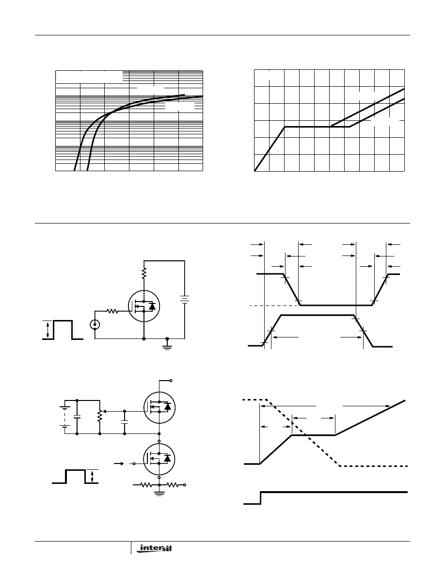
Test Circuits and Waveforms
FIGURE 14. SWITCHING TIME TEST CIRCUIT
FIGURE 15. RESISTIVE SWITCHING WAVEFORMS
FIGURE 16. GATE CHARGE TEST CIRCUIT
FIGURE 17. GATE CHARGE WAVEFORMS
Typical Performance Curves
Unless Otherwise Specified (Continued)
0
0.5
1.0
1.5
2.0
2.5
3.0
V
SD
, SOURCE TO DRAIN VOLTAGE (V)
10
3
10
2
10
1
10
0
10
-1
I
SD
, SOURCE T
O
DRAIN CURRENT (A)
PULSE DURATION = 80
µ
s
T
J
= 25
o
C
T
J
= 150
o
C
DUTY CYCLE = 0.5% MAX
15
10
5
0
0
10
20
30
40
50
Q
g
, GATE CHARGE (nC)
V
GS
, GA
TE T
O
SOURCE V
O
L
T
A
GE (V)
I
D
= 45A
V
DS
= 10V
V
DS
= 40V
V
GS
R
L
R
G
DUT
+
-
V
DD
t
ON
t
d(ON)
t
r
90%
10%
V
DS
90%
10%
t
f
t
d(OFF)
t
OFF
90%
50%
50%
10%
PULSE WIDTH
V
GS
0
0
0.3
µ
F
12V
BATTERY
50k
Ω
V
DS
S
DUT
D
G
I
g(REF)
0
(ISOLATED
V
DS
0.2
µ
F
CURRENT
REGULATOR
I
D
CURRENT
SAMPLING
I
G
CURRENT
SAMPLING
SUPPLY)
RESISTOR
RESISTOR
SAME TYPE
AS DUT
Q
g(TOT)
Q
gd
Q
gs
V
DS
0
V
GS
V
DD
I
g(REF)
0
BUZ11

4-10
All Intersil semiconductor products are manufactured, assembled and tested under ISO9000 quality systems certification.
Intersil semiconductor products are sold by description only. Intersil Corporation reserves the right to make changes in circuit design and/or specifications at any time with-
out notice. Accordingly, the reader is cautioned to verify that data sheets are current before placing orders. Information furnished by Intersil is believed to be accurate and
reliable. However, no responsibility is assumed by Intersil or its subsidiaries for its use; nor for any infringements of patents or other rights of third parties which may result
from its use. No license is granted by implication or otherwise under any patent or patent rights of Intersil or its subsidiaries.
For information regarding Intersil Corporation and its products, see web site http://www.intersil.com
Sales Office Headquarters
NORTH AMERICA
Intersil Corporation
P. O. Box 883, Mail Stop 53-204
Melbourne, FL 32902
TEL: (407) 724-7000
FAX: (407) 724-7240
EUROPE
Intersil SA
Mercure Center
100, Rue de la Fusee
1130 Brussels, Belgium
TEL: (32) 2.724.2111
FAX: (32) 2.724.22.05
ASIA
Intersil (Taiwan) Ltd.
7F-6, No. 101 Fu Hsing North Road
Taipei, Taiwan
Republic of China
TEL: (886) 2 2716 9310
FAX: (886) 2 2715 3029
BUZ11
Wyszukiwarka
Podobne podstrony:
intersekcja geologiczna
Programowanie Interstarid 13046
Pierwotna i wtórna intersubiektywność wykłąd 5
Intersubiektywny kontekst doświadczenia ciała w fenomenologi Husserla
BUZ11
1---PAGO-osw.-chł.-baza, 1---Eksporty-all, 1---Eksporty---, 12---agencje-celne, 1---A.C.-Intersped-B
praca zaliczeniowa ze wstymulacji aktywności werbalnej w pracy przedszkola metoda intersemiotyczna
Analiza otoczenia firmy Interspeed sp. z o.o., strategia
PODSTAWOWE WIADOMOŚCI Z INTERSEKCJI GEOLOGICZNEJ
POETYKA INTERSEMIOTYCZNA
PRZEKŁAD INTERSEMIOTYCZNY, Pedagogika, Edukacja wczesnoszkolna - polski
PRZEKŁAD INTERSEMIOTYCZNY W KSZTAŁCENIU LITERACKIM
BUZ11
metoda przekładu intersemiotycznego dyduchowa
scenariusz - metoda przekładu intersemiotycznego, Edukacja polonistyczna
Ćwiczenie interSIT kalka, 7 SEM IŚ, sYSTEMY INFORMACJI PRZESTRZENNEJ
więcej podobnych podstron