
Hudgins, J.L., Bogart, Jr., T.F., Mayaram, K., Kennedy, M.P., Kolumbán, G. “Nonlinear
Circuits”
The Electrical Engineering Handbook
Ed. Richard C. Dorf
Boca Raton: CRC Press LLC, 2000

© 2000 by CRC Press LLC
5
Nonlinear Circuits
Diodes • Rectifiers
Limiting Circuits • Precision Rectifying Circuits
Harmonic Distortion • Power-Series Method • Differential-Error
Method • Three-Point Method • Five-Point Method •
Intermodulation Distortion • Triple-Beat Distortion • Cross
Modulation • Compression and Intercept Points • Crossover
Distortion • Failure-to-Follow Distortion • Frequency Distortion •
Phase Distortion • Computer Simulation of Distortion Components
Elements of Chaotic Digital Communications Systems • Chaotic Digital
Modulation Schemes • Low-Pass Equivalent Models for Chaotic
Communications Systems • Multipath Performance of FM-DCSK
5.1 Diodes and Rectifiers
Jerry L. Hudgins
generally refers to a two-terminal solid-state semiconductor device that presents a low impedance to
current flow in one direction and a high impedance to current flow in the opposite direction. These properties
allow the diode to be used as a one-way current valve in electronic circuits.
Rectifiers
are a class of circuits
whose purpose is to convert ac waveforms (usually sinusoidal and with zero average value) into a waveform
that has a significant non-zero average value (dc component). Simply stated, rectifiers are ac-to-dc energy
converter circuits. Most rectifier circuits employ diodes as the principal elements in the energy conversion
process; thus the almost inseparable notions of diodes and rectifiers. The general electrical characteristics of
common diodes and some simple rectifier topologies incorporating diodes are discussed.
Diodes
Most diodes are made from a host crystal of silicon (Si) with appropriate impurity elements introduced to
modify, in a controlled manner, the electrical characteristics of the device. These diodes are the typical
) devices used in electronic circuits. Another type is the
(unipolar),
produced by placing a metal layer directly onto the semiconductor [Schottky, 1938; Mott, 1938]. The metal-
semiconductor interface serves the same function as the
pn
-junction in the common diode structure. Other
semiconductor materials such as gallium-arsenide (GaAs) and silicon-carbide (SiC) are also in use for new and
specialized applications of diodes. Detailed discussion of diode structures and the physics of their operation
can be found in later paragraphs of this section.
The electrical circuit symbol for a bipolar diode is shown in
. The polarities associated with the
forward voltage drop for forward current flow are also included. Current or voltage opposite to the polarities
indicated in
are considered to be negative values with respect to the diode conventions shown.
Jerry L. Hudgins
University of South Carolina
Theodore F. Bogart, Jr.
University of Southern Mississippi
Kartikeya Mayaram
Washington State University
Michael Peter Kennedy
University College Dublin
Géza Kolumbán
Technical University of Budapest
© 2000 by CRC Press LLC
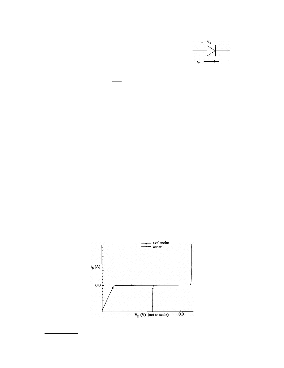
The characteristic curve shown in
is representative of the current-
voltage dependencies of typical diodes. The diode conducts forward current
with a small forward voltage drop across the device, simulating a closed
switch. The relationship between the forward current and forward voltage
is approximately given by the Shockley diode equation [Shockley, 1949]:
(5.1)
where
I
s
is the leakage current through the diode,
q
is the electronic charge,
n
is a correction factor,
k
is
Boltzmann’s constant, and
T
is the temperature of the semiconductor. Around the knee of the curve in
is a positive voltage that is termed the turn-on or sometimes the threshold voltage for the diode. This value is
an approximate voltage above which the diode is considered turned “on” and can be modeled to first degree
as a closed switch with constant forward drop. Below the threshold voltage value the diode is considered weakly
conducting and approximated as an open switch. The exponential relationship shown in Eq. (5.1) means that
the diode forward current can change by orders of magnitude before there is a large change in diode voltage,
thus providing the simple circuit model during conduction. The nonlinear relationship of Eq. (5.1) also provides
a means of frequency mixing for applications in modulation circuits.
Reverse voltage applied to the diode causes a small leakage current (negative according to the sign convention)
to flow that is typically orders of magnitude lower than current in the forward direction. The diode can withstand
reverse voltages up to a limit determined by its physical construction and the semiconductor material used.
Beyond this value the reverse voltage imparts enough energy to the charge carriers to cause large increases in
current. The mechanisms by which this current increase occurs are impact ionization (avalanche) [McKay,
1954] and a tunneling phenomenon (Zener breakdown) [Moll, 1964]. Avalanche breakdown results in large
power dissipation in the diode, is generally destructive, and should be avoided at all times. Both breakdown
regions are superimposed in
for comparison of their effects on the shape of the diode characteristic
curve. Avalanche breakdown occurs for reverse applied voltages in the range of volts to kilovolts depending on
the exact design of the diode. Zener breakdown occurs at much lower voltages than the avalanche mechanism.
Diodes specifically designed to operate in the Zener breakdown mode are used extensively as voltage regulators
in regulator integrated circuits and as discrete components in large regulated power supplies.
During forward conduction the power loss in the diode can become excessive for large current flow. Schottky
diodes have an inherently lower turn-on voltage than
pn
-junction diodes and are therefore more desirable in
applications where the energy losses in the diodes are significant (such as output rectifiers in switching power
supplies). Other considerations such as recovery characteristics from forward conduction to reverse blocking
FIGURE 5.2
A typical diode dc characteristic curve showing the current dependence on voltage.
FIGURE 5.1
Circuit symbol for a
bipolar diode indicating the polar-
ity associated with the forward
voltage and current directions.
i
I
qV
nkT
D
s
D
=
æ
èç
ö
ø÷
é
ë
ê
ê
ù
û
ú
ú
exp – 1
© 2000 by CRC Press LLC
may also make one diode type more desirable than another. Schottky diodes conduct current with one type of
charge carrier and are therefore inherently faster to turn off than bipolar diodes. However, one of the limitations
of Schottky diodes is their excessive forward voltage drop when designed to support reverse biases above about
200 V. Therefore, high-voltage diodes are the
pn
-junction type.
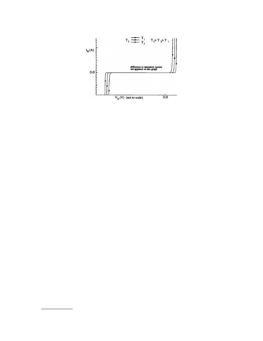
The effects due to an increase in the temperature in a bipolar diode are many. The forward voltage drop
during conduction will decrease over a large current range, the reverse leakage current will increase, and the
reverse avalanche breakdown voltage (
V
BD
) will increase as the device temperature climbs. A family of static
characteristic curves highlighting these effects is shown in
where
T
3
>
T
2
>
T
1
. In addition, a major
effect on the switching characteristic is the increase in the reverse recovery time during turn-off. Some of the
key parameters to be aware of when choosing a diode are its repetitive peak inverse voltage rating,
V
RRM
(relates
to the avalanche breakdown value), the peak forward surge current rating,
I
FSM
(relates to the maximum
allowable transient heating in the device), the average or rms current rating,
I
O
(relates to the steady-state
heating in the device), and the reverse recovery time,
t
rr
(relates to the switching speed of the device).
Rectifiers
This section discusses some simple
circuits that are commonly encountered. The term
uncontrolled
refers to the absence of any control signal necessary to operate the primary switching elements (diodes
)
in the rectifier circuit. The discussion of controlled rectifier circuits, and the controlled switches themselves, is
more appropriate in the context of power electronics applications [Hoft, 1986]. Rectifiers are the fundamental
building block in dc power supplies of all types and in dc power transmission used by some electric utilities.
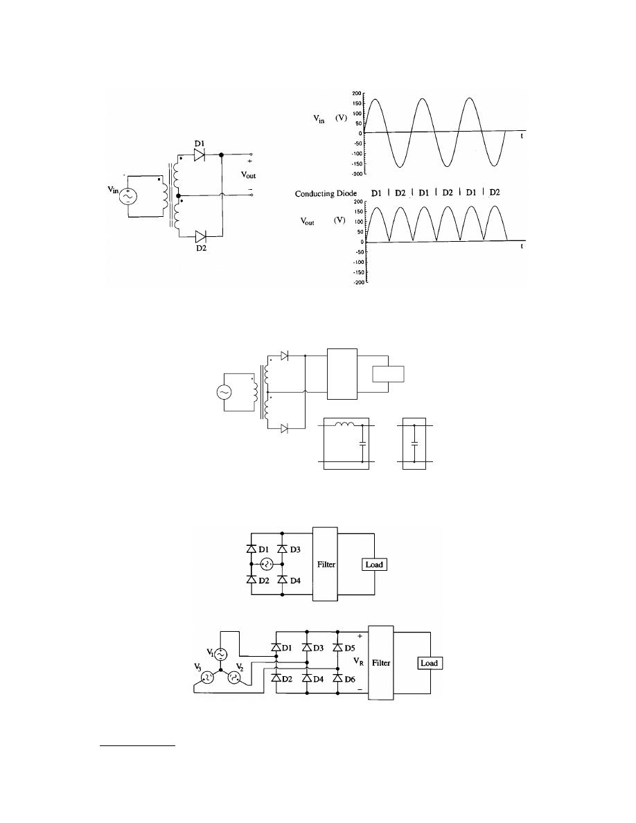
A single-phase full-wave rectifier circuit with the accompanying input and output voltage waveforms is shown
. This topology makes use of a center-tapped transformer with each diode conducting on opposite
half-cycles of the input voltage. The forward drop across the diodes is ignored on the output graph, which is
a valid approximation if the peak voltages of the input and output are large compared to 1 V. The circuit changes
a sinusoidal waveform with no dc component (zero average value) to one with a dc component of 2
V
peak
/
p
.
The rms value of the output is 0.707
V
peak
.
The dc value can be increased further by adding a low-pass filter in cascade with the output. The usual form
of this filter is a shunt capacitor or an LC filter as shown in
. The resonant frequency of the LC filter
should be lower than the fundamental frequency of the rectifier output for effective performance. The ac portion
of the output signal is reduced while the dc and rms values are increased by adding the filter. The remaining
ac portion of the output is called the
Though somewhat confusing, the transformer, diodes, and filter
are often collectively called the rectifier circuit.
Another circuit topology commonly encountered is the bridge rectifier.
illustrates single- and
three-phase versions of the circuit. In the single-phase circuit diodes D1 and D4 conduct on the positive
half-cycle of the input while D2 and D3 conduct on the negative half-cycle of the input. Alternate pairs of
diodes conduct in the three-phase circuit depending on the relative amplitude of the source signals.
FIGURE 5.3
The effects of temperature variations on the forward voltage drop and the avalanche breakdown voltage in
a bipolar diode.
© 2000 by CRC Press LLC
FIGURE 5.4
A single-phase full-wave rectifier circuit using a center-tapped transformer with the associated input and
output waveforms.
FIGURE 5.5
A single-phase full-wave rectifier with the addition of an output filter.
FIGURE 5.6
Single- and three-phase bridge rectifier circuits.
V
in
L
C
C
+
–
Filter
Load
© 2000 by CRC Press LLC
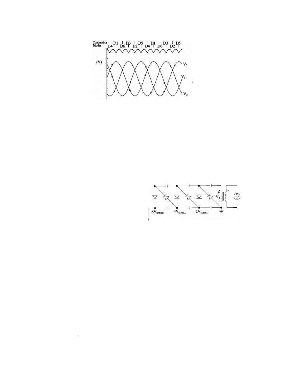
The three-phase inputs with the associated rectifier output voltage are shown in
as they would appear
without the low-pass filter section. The three-phase bridge rectifier has a reduced ripple content of 4% as
compared to a ripple content of 47% in the single-phase bridge rectifier [Milnes, 1980]. The corresponding
diodes that conduct are also shown at the top of the figure. This output waveform assumes a purely resistive
load connected as shown in Fig. 5.6. Most loads (motors, transformers, etc.) and many sources (power grid)
include some inductance, and in fact may be dominated by inductive properties. This causes phase shifts
between the input and output waveforms. The rectifier output may thus vary in shape and phase considerably
from that shown in Fig. 5.7 [Kassakian et al., 1991]. When other types of switches are used in these circuits the
inductive elements can induce large voltages that may damage sensitive or expensive components. Diodes are
used regularly in such circuits to shunt current and clamp induced voltages at low levels to protect expensive
components such as electronic switches.
One variation of the typical rectifier is the Cockroft-
Walton circuit used to obtain high voltages without the
necessity of providing a high-voltage transformer. The
circuit in
multiplies the peak secondary voltage
by a factor of six. The steady-state voltage level at each
filter capacitor node is shown in the figure. Adding
additional stages increases the load voltage further. As
in other rectifier circuits, the value of the capacitors
will determine the amount of ripple in the output
waveform for given load resistance values. In general,
the capacitors in a lower voltage stage should be larger
than in the next highest voltage stage.
Defining Terms
Bipolar device:
Semiconductor electronic device that uses positive and negative charge carriers to conduct
electric current.
Diode:
Two-terminal solid-state semiconductor device that presents a low impedance to current flow in one
direction and a high impedance to current flow in the opposite direction.
pn
-junction:
Metallurgical interface of two regions in a semiconductor where one region contains impurity
elements that create equivalent positive charge carriers (
p
-type) and the other semiconductor region
contains impurities that create negative charge carriers (
n
-type).
Ripple:
The ac (time-varying) portion of the output signal from a rectifier circuit.
Schottky diode:
A diode formed by placing a metal layer directly onto a unipolar semiconductor substrate.
Uncontrolled rectifier:
A rectifier circuit employing switches that do not require control signals to operate
them in their “on” or “off ” states.
FIGURE 5.7
Three-phase rectifier output compared to the input signals. The input signals as well as the conducting diode
labels are those referenced to Fig. 5.6.
FIGURE 5.8 Cockroft-Walton circuit used for voltage
multiplication.

© 2000 by CRC Press LLC
Related Topics
22.2 Diodes • 30.1 Power Semiconductor Devices
References
R.G. Hoft,
Semiconductor Power Electronics,
New York: Van Nostrand Reinhold, 1986.
J.G. Kassakian, M.F. Schlecht, and G.C. Verghese,
Principles of Power Electronics,
Reading, Mass.: Addison-
Wesley, 1991.
K.G. McKay, “Avalanche breakdown in silicon,”
Physical Review,
vol. 94, p. 877, 1954.
A.G. Milnes,
Semiconductor Devices and Integrated Electronics,
New York: Van Nostrand Reinhold, 1980.
J.L. Moll,
Physics of Semiconductors,
New York: McGraw-Hill, 1964.
N.F. Mott, “Note on the contact between a metal and an insulator or semiconductor,”
Proc. Cambridge Philos.
Soc.,
vol. 34, p. 568, 1938.
W. Schottky, “Halbleitertheorie der Sperrschicht,”
Naturwissenschaften,
vol. 26, p. 843, 1938.
W. Shockley, “The theory of p-n junctions in semiconductors and p-n junction transistors,”
Bell System Tech.
J.,
vol. 28, p. 435, 1949.
Further Information
A good introduction to solid-state electronic devices with a minimum of mathematics and physics is
Solid State
Electronic Devices,
3rd edition, by B.G. Streetman, Prentice-Hall, 1989. A rigorous and more detailed discussion
is provided in
Physics of Semiconductor Devices,
2nd edition, by S.M. Sze, John Wiley & Sons, 1981. Both of
these books discuss many specialized diode structures as well as other semiconductor devices. Advanced material
on the most recent developments in semiconductor devices, including diodes, can be found in technical journals
such as the
IEEE Transactions on Electron Devices, Solid State Electronics,
and
Journal of Applied Physics.
A good
summary of advanced rectifier topologies and characteristics is given in
Basic Principles of Power Electronics
by
K. Heumann, Springer-Verlag, 1986. Advanced material on rectifier designs as well as other power electronics
circuits can be found in
IEEE Transactions on Power Electronics, IEEE Transactions on Industry Applications,
and
the
EPE Journal.
Two good industry magazines that cover power devices such as diodes and power converter
circuitry are
Power Control and Intelligent Motion
(PCIM) and
Power Technics.
5.2 Limiters
1
Theodore F. Bogart, Jr.
Limiters
are named for their ability to limit voltage excursions at the output of a circuit whose input may
undergo unrestricted variations. They are also called
clipping circuits
because waveforms having rounded peaks
that exceed the limit(s) imposed by such circuits appear, after limiting, to have their peaks flattened, or “clipped”
off.
may be designed to clip positive voltages at a certain level, negative voltages at a different level, or
to do both. The simplest types consist simply of diodes and dc voltage sources, while more elaborate designs
incorporate operational amplifiers.
Limiting Circuits
shows how the transfer characteristics of limiting circuits reflect the fact that outputs are clipped at
certain levels. In each of the examples shown, note that the characteristic becomes horizontal at the output
level where clipping occurs. The horizontal line means that the output remains constant regardless of the input
level in that region. Outside of the clipping region, the transfer characteristic is simply a line whose slope equals
1
Excerpted from T.F. Bogart, Jr.,
Electronic Devices and Circuits,
3rd ed., Columbus, Ohio:Macmillan/Merrill, 1993,
pp. 689–697. With permission.
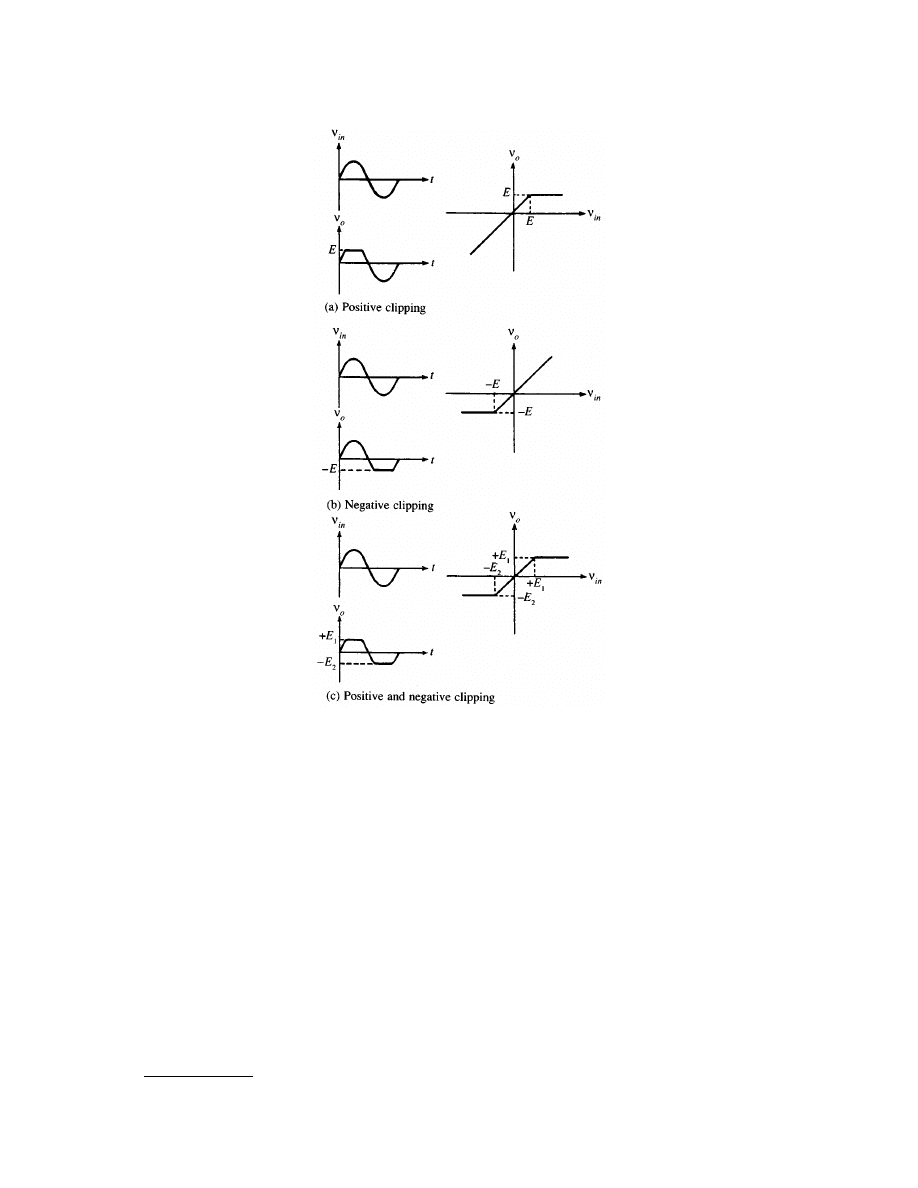
© 2000 by CRC Press LLC
the gain of the device. This is the region of linear operation. In these examples, the devices are assumed to have
unity gain, so the slope of each line in the linear region is 1.
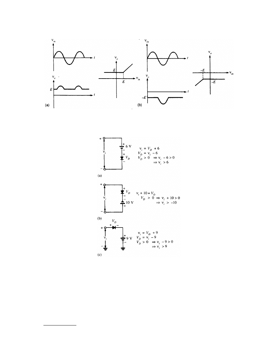
illustrates a somewhat different kind of limiting action. Instead of the positive or negative peaks
being clipped, the output follows the input when the signal is above or below a certain level. The transfer
characteristics show that linear operation occurs only when certain signal levels are reached and that the output
remains constant below those levels. This form of limiting can also be thought of as a special case of that shown
in Fig. 5.9. Imagine, for example, that the clipping level in Fig. 5.9(b) is raised to a positive value; then the
result is the same as Fig. 5.10(a).
Limiting can be accomplished using
Such circuits rely on the fact that diodes have very low
impedances when they are forward biased and are essentially open circuits when reverse biased. If a certain
point in a circuit, such as the output of an amplifier, is connected through a very small impedance to a
constant
voltage, then the voltage at the circuit point cannot differ significantly from the constant voltage. We say in
this case that the point is
clamped
to the fixed voltage. An ideal, forward-biased diode is like a closed switch,
so if it is connected between a point in a circuit and a fixed voltage source, the diode very effectively holds the
point to the fixed voltage. Diodes can be connected in operational amplifier circuits, as well as other circuits,
FIGURE 5.9
Waveforms and transfer characteristics of limiting circuits. (
Source:
T.F. Bogart, Jr.,
Electronic Devices and
Circuits,
3rd ed., Columbus, Ohio: Macmillan/Merrill, 1993, p. 676. With permission.)
© 2000 by CRC Press LLC
in such a way that they become forward biased when a signal reaches a certain voltage. When the forward-biasing
level is reached, the diode serves to hold the output to a fixed voltage and thereby establishes a clipping level.
A biased diode is simply a diode connected to a fixed voltage source. The value and polarity of the voltage
source determine what value of total voltage across the combination is necessary to forward bias the diode.
shows several examples. (In practice, a series resistor would be connected in each circuit to limit
current flow when the diode is forward biased.) In each part of the figure, we can write Kirchhoff ’s voltage law
FIGURE 5.10
Another form of clipping. Compare with Fig. 5.9. (
Source:
T.F. Bogart, Jr.,
Electronic Devices and Circuits,
3rd ed., Columbus, Ohio: Macmillan/Merrill, 1993, p. 690. With permission.)
FIGURE 5.11
Examples of biased diodes and the signal voltages
v
i
required to forward bias them. (Ideal diodes are
assumed.) In each case, we solve for the value of
v
i
that is necessary to make
V
D
> 0. (
Source:
T.F. Bogart, Jr.,
Electronic
Devices and Circuits,
3rd ed., Columbus, Ohio: Macmillan/Merrill, 1993, p. 691. With permission.)
© 2000 by CRC Press LLC
around the loop to determine the value of input voltage
v
i
that is necessary to forward bias the diode. Assuming
that the diodes are ideal (neglecting their forward voltage drops), we determine the value
v
i
necessary to forward
bias each diode by determining the value
v
i
necessary to make
v
D
> 0. When
v
i
reaches the voltage necessary
to make
V
D
> 0, the diode becomes forward biased and the signal source is forced to, or held at, the dc source
voltage. If the forward voltage drop across the diode is not neglected, the clipping level is found by determining
the value of
v
i
necessary to make
V
D
greater than that forward drop (e.g.,
V
D
> 0.7 V for a silicon diode).
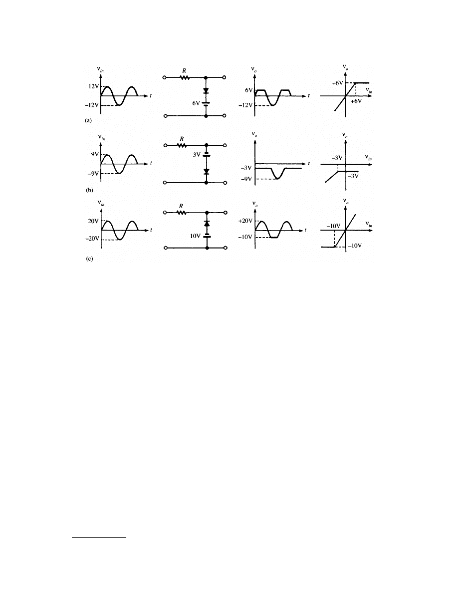
shows three examples of clipping circuits using ideal biased diodes and the waveforms that result
when each is driven by a sine-wave input. In each case, note that the output equals the dc source voltage when
the input reaches the value necessary to forward bias the diode. Note also that the type of clipping we showed
in Fig. 5.9 occurs when the fixed bias voltage tends to
reverse
bias the diode, and the type shown in Fig. 5.10
occurs when the fixed voltage tends to
forward
bias the diode. When the diode is reverse biased by the input
signal, it is like an open circuit that disconnects the dc source, and the output follows the input. These circuits
are called
parallel
clippers because the biased diode is in parallel with the output. Although the circuits behave
the same way whether or not one side of the dc voltage source is connected to the common (low) side of the
input and output, the connections shown in Fig. 5.12(a) and (c) are preferred to that in (b), because the latter
uses a floating source.
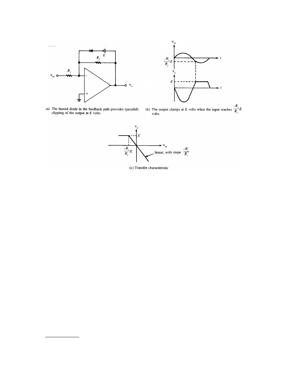
shows a biased diode connected in the feedback path of an inverting operational amplifier. The
diode is in parallel with the feedback resistor and forms a parallel clipping circuit like that shown in Fig. 5.12.
In an operational amplifier circuit,
v
–
» v
+
, and since v
+
= 0 V in this circuit, v
–
is approximately 0 V (virtual
ground). Thus, the voltage across R
f
is the same as the output voltage v
o
. Therefore, when the output voltage
reaches the bias voltage E, the output is held at E volts. Figure 5.13(b) illustrates this fact for a sinusoidal input.
So long as the diode is reverse biased, it acts like an open circuit and the amplifier behaves like a conventional
inverting amplifier. Notice that output clipping occurs at input voltage –(R
1
/R
f
)E, since the amplifier inverts and
has closed-loop gain magnitude R
f
/R
1
. The resulting transfer characteristic is shown in Fig. 5.13(c).
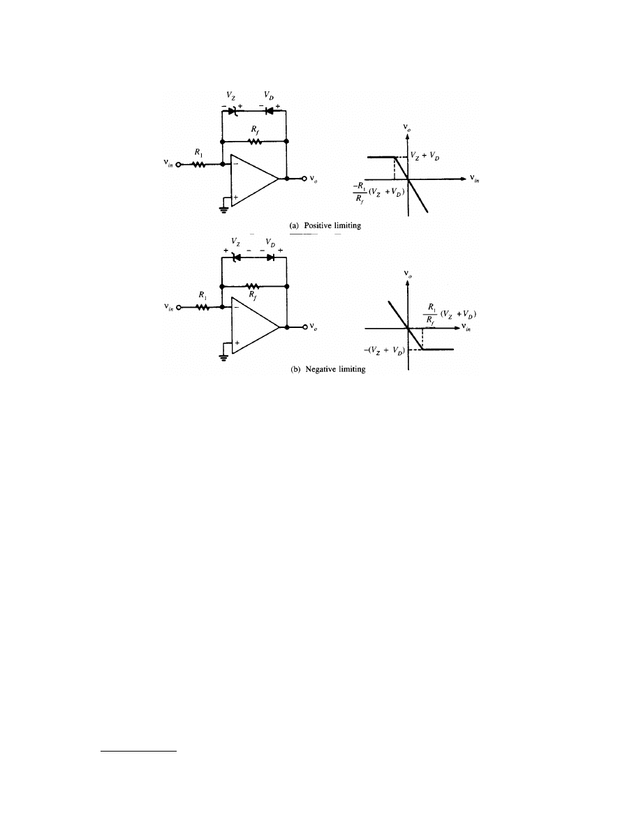
In practice, the biased diode shown in the feedback of Fig. 5.13(a) is often replaced by a Zener diode in series
with a conventional diode. This arrangement eliminates the need for a floating voltage source. Zener diodes
FIGURE 5.12 Examples of parallel clipping circuits. (Source: T.F. Bogart, Jr., Electronic Devices and Circuits, 3rd ed.,
Columbus, Ohio: Macmillan/Merrill, 1993, p. 692. With permission.)
© 2000 by CRC Press LLC
are in many respects functionally equivalent to biased diodes.
shows two operational amplifier
clipping circuits using Zener diodes. The Zener diode conducts like a conventional diode when it is forward
biased, so it is necessary to connect a reversed diode in series with it to prevent shorting of R
f
. When the reverse
voltage across the Zener diode reaches V
Z
, the diode breaks down and conducts heavily, while maintaining an
essentially constant voltage, V
Z
, across it. Under those conditions, the total voltage across R
f
, i.e., v
o
, equals V
Z
plus the forward drop, V
D
, across the conventional diode.
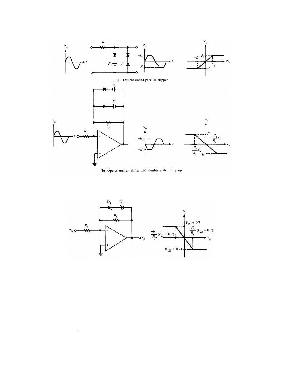
shows double-ended limiting circuits, in which both positive and negative peaks of the output
waveform are clipped. Figure 5.15(a) shows the conventional parallel clipping circuit and (b) shows how double-
ended limiting is accomplished in an operational amplifier circuit. In each circuit, note that no more than one
diode is forward biased at any given time and that both diodes are reverse biased for –E
1
< v
o
< E
2
, the linear
region.
shows a double-ended limiting circuit using back-to-back Zener diodes. Operation is similar to
that shown in Fig. 5.14, but no conventional diode is required. Note that diode D
1
is conducting in a forward
direction when D
2
conducts in its reverse breakdown (Zener) region, while D
2
is forward biased when D
1
is
conducting in its reverse breakdown region. Neither diode conducts when –(V
Z2
+ 0.7) < v
o
< (V
Z1
+ 0.7),
which is the region of linear amplifier operation.
Precision Rectifying Circuits
A rectifier is a device that allows current to pass through it in one direction only. A diode can serve as a rectifier
because it permits generous current flow in only one direction—the direction of forward bias. Rectification is
the same as limiting at the 0-V level: all of the waveform below (or above) the zero-axis is eliminated. However,
a diode rectifier has certain intervals of nonconduction and produces resulting “gaps” at the zero-crossing points
of the output voltage, due to the fact that the input must overcome the diode drop (0.7 V for silicon) before
FIGURE 5.13
An operational amplifier limiting circuit. (Source: T.F. Bogart, Jr., Electronic Devices and Circuits, 3rd ed.,
Columbus, Ohio:Macmillan/Merrill, 1993, p. 693. With permission.)
© 2000 by CRC Press LLC
conduction begins. In power-supply applications, where input voltages are quite large, these gaps are of no
concern. However, in many other applications, especially in instrumentation, the 0.7-V drop can be a significant
portion of the total input voltage swing and can seriously affect circuit performance. For example, most ac
instruments rectify ac inputs so they can be measured by a device that responds to dc levels. It is obvious that
small ac signals could not be measured if it were always necessary for them to reach 0.7 V before rectification
could begin. For these applications, precision rectifiers are necessary.
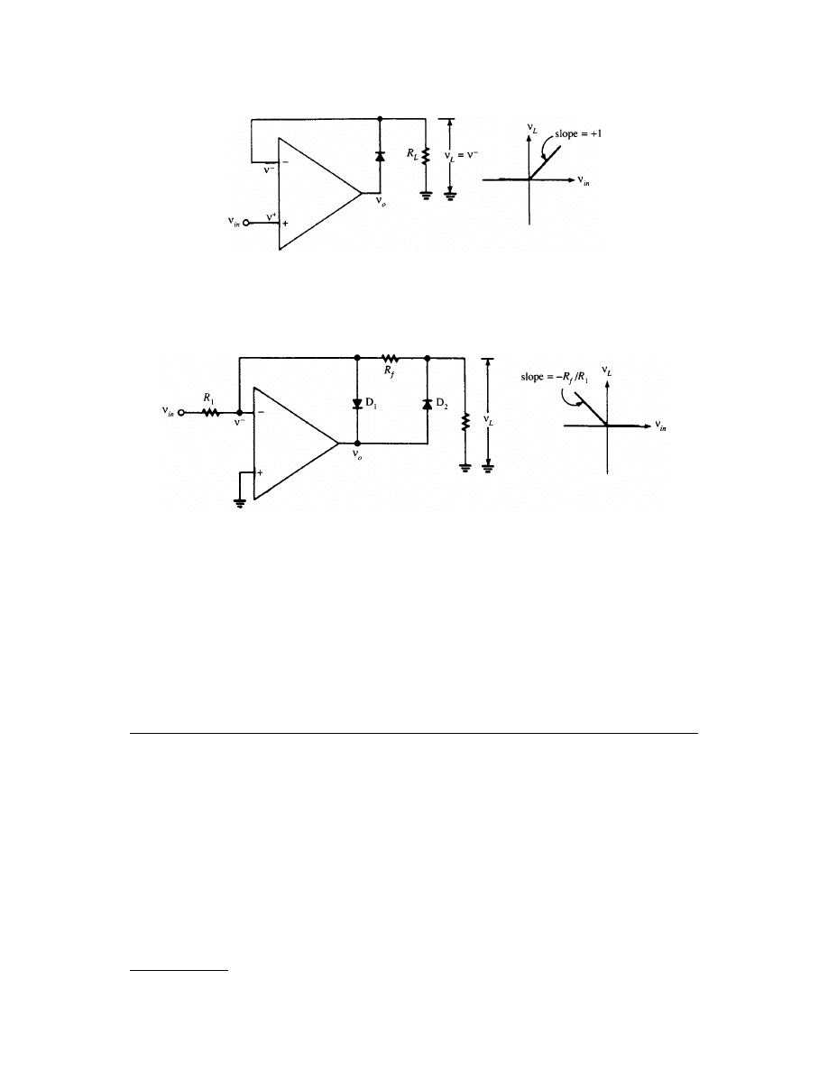
shows one way to obtain precision rectification using an operational amplifier and a diode. The
circuit is essentially a noninverting voltage follower (whose output follows, or duplicates, its input) when the
diode is forward biased. When v
in
is positive, the output of the amplifier, v
o
, is positive, the diode is forward
biased, and a low-resistance path is established between v
o
and v
–
, as necessary for a voltage follower. The load
voltage, v
L
, then follows the positive variations of v
in
= v
+
. Note that even a very small positive value of v
in
will
cause this result, because of the large differential gain of the amplifier. That is, the large gain and the action of
the feedback cause the usual result that v
+
' v
–
. Note also that the drop across the diode does not appear in v
L
.
When the input goes negative, v
o
becomes negative, and the diode is reverse biased. This effectively opens
the feedback loop, so v
L
no longer follows v
in
. The amplifier itself, now operating open-loop, is quickly driven
to its maximum negative output, thus holding the diode well into reverse bias.
Another precision rectifier circuit is shown in
. In this circuit, the load voltage is an amplified and
inverted version of the negative variations in the input signal, and is 0 when the input is positive. Also in contrast
with the previous circuit, the amplifier in this rectifier is not driven to one of its output extremes. When v
in
is
negative, the amplifier output, v
o
, is positive, so diode D
1
is reverse biased and diode D
2
is forward biased. D
1
is open and D
2
connects the amplifier output through R
f
to v
–
. Thus, the circuit behaves like an ordinary
inverting amplifier with gain –R
f
/R
1
. The load voltage is an amplified and inverted (positive) version of the
negative variations in v
in
. When v
in
becomes positive, v
o
is negative, D
1
is forward biased, and D
2
is reverse
biased. D
1
shorts the output v
o
to v
–
, which is held at virtual ground, so v
L
is 0.
FIGURE 5.14
Operational amplifier limiting circuits using Zener diodes. (Source: T.F. Bogart, Jr., Electronic Devices and
Circuits, 3rd ed., Columbus, Ohio: Macmillan/Merrill, 1993, p. 694. With permission.)
© 2000 by CRC Press LLC
Defining Terms
Biased diode:
A diode connected in series with a dc voltage source in order to establish a clipping level.
Clipping occurs when the voltage across the combination is sufficient to forward bias the diode.
Limiter:
A device or circuit that restricts voltage excursions to prescribed level(s). Also called a clipping circuit.
Related Topics
5.1 Diodes and Rectifiers • 27.1 Ideal and Practical Models
FIGURE 5.15
Double-ended clipping, or limiting. (Source: T.F. Bogart, Jr., Electronic Devices and Circuits, 3rd ed., Colum-
bus, Ohio: Macmillan/Merrill, 1993, p. 695. With permission.)
FIGURE 5.16
A double-ended limiting circuit using Zener diodes. (Source: T.F. Bogart, Jr., Electronic Devices and Circuits,
3rd ed., Columbus, Ohio: Macmillan/Merrill, 1993, p. 695. With permission.)
© 2000 by CRC Press LLC
References
W.H. Baumgartner, Pulse Fundamentals and Small-Scale Digital Circuits, Reston, Va.: Reston Publishing, 1985.
T. F. Bogart, Jr., Electronic Devices and Circuits, 3rd ed., Columbus, Ohio: Macmillan/Merrill, 1993.
R.A. Gayakwad, Op-Amps and Linear Integrated Circuit Technology, Englewood Cliffs, N.J.: Prentice-Hall, 1983.
A.S. Sedra and K.C. Smith, Microelectronic Circuits, New York: CBS College Publishing, 1982.
H. Zanger, Semiconductor Devices and Circuits, New York: John Wiley & Sons, 1984.
5.3 Distortion
Kartikeya Mayaram
The diode was introduced in the previous sections as a nonlinear device that is used in rectifiers and limiters.
These are applications that depend on the nonlinear nature of the diode. Typical electronic systems are
composed not only of diodes but also of other nonlinear devices such as transistors (Section III). In analog
applications transistors are used to amplify weak signals (amplifiers) and to drive large loads (output stages).
For such situations it is desirable that the output be an amplified true reproduction of the input signal; therefore,
the transistors must operate as linear devices. However, the inherent nonlinearity of transistors results in an
output which is a “distorted” version of the input.
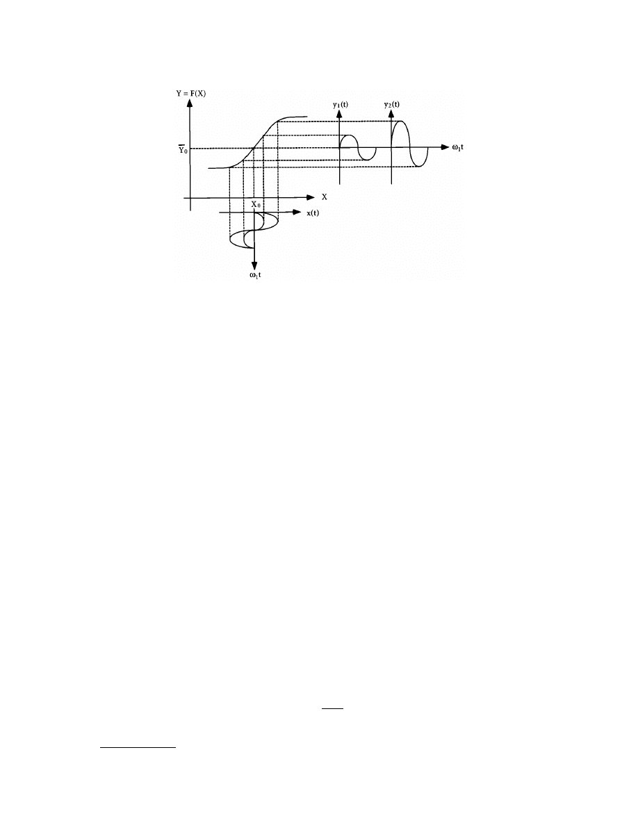
The distortion due to a nonlinear device is illustrated in
. For an input X the output is Y = F(X)
where F denotes the nonlinear transfer characteristics of the device; the dc operating point is given by X
0
.
Sinusoidal input signals of two different amplitudes are applied and the output responses corresponding to
these inputs are also shown.
FIGURE 5.17
A precision rectifier. When v
in
is positive, the diode is forward biased, and the amplifier behaves like a voltage
follower, maintaining v
+
' v
–
= v
L
. (Source: T.F. Bogart, Jr., Electronic Devices and Circuits, 3rd ed., Columbus, Ohio:
Macmillan/Merrill, 1993, p. 696. With permission.)
FIGURE 5.18
A precision rectifier circuit that amplifies and inverts the negative variations in the input voltage. (Source:
T.F. Bogart, Jr., Electronic Devices and Circuits, 3rd ed., Columbus, Ohio: Macmillan/Merrill, 1993, p. 697. With permission.)
© 2000 by CRC Press LLC
For an input signal of small amplitude the output faithfully follows the input, whereas for large-amplitude
signals the output is distorted; a flattening occurs at the negative peak value. The distortion in amplitude results
in the output having frequency components that are integer multiples of the input frequency, harmonics, and
this type of distortion is referred to as
The distortion level places a restriction on the amplitude of the input signal that can be applied to an
electronic system. Therefore, it is essential to characterize the distortion in a circuit. In this section different
types of distortion are defined and techniques for distortion calculation are presented. These techniques are
applicable to simple circuit configurations. For larger circuits a circuit simulation program is invaluable.
Harmonic Distortion
When a sinusoidal signal of a single frequency is applied at the input of a nonlinear device or circuit, the
resulting output contains frequency components that are integer multiples of the input signal. These harmonics
are generated by the nonlinearity of the circuit and the harmonic distortion is measured by comparing the
magnitudes of the harmonics with the fundamental component (input frequency) of the output.
Consider the input signal to be of the form:
x(t) = X
1
cos
w
1
t (5.2)
where f
1
=
w
1
/2
p is the frequency and X
1
is the amplitude of the input signal. Let the output of the nonlinear
circuit be
y(t) = Y
0
+ Y
1
cos
w
1
t + Y
2
cos 2
w
1
t + Y
3
cos 3
w
1
t + . . . (5.3)
where Y
0
is the dc component of the output, Y
1
is the amplitude of the fundamental component, and Y
2
, Y
3
are
the amplitudes of the second and third harmonic components. The second harmonic distortion factor (HD
2
),
the third harmonic distortion factor (HD
3
), and the nth harmonic distortion factor (HD
n
) are defined as
(5.4)
FIGURE 5.19
DC transfer characteristics of a nonlinear circuit and the input and output waveforms. For a large input
amplitude the output is distorted.
HD
2
2
1
= *
*
*
*
Y
Y

© 2000 by CRC Press LLC
(5.5)
(5.6)
The
(THD) of a waveform is defined to be the ratio of the rms (root-mean-square)
value of the harmonics to the amplitude of the fundamental component.
(5.7)
THD can be expressed in terms of the individual
(5.8)
Various methods for computing the harmonic distortion factors are described next.
Power-Series Method
In this method a truncated power-series expansion of the dc transfer characteristics of a nonlinear circuit is
used. Therefore, the method is suitable only when energy storage effects in the nonlinear circuit are negligible
and the input signal is small. In general, the input and output signals comprise both dc and time-varying
components. For distortion calculation we are interested in the time-varying or incremental components around
a quiescent
1
operating point. For the transfer characteristic of Fig. 5.19, denote the quiescent operating condi-
tions by X
0
and
–
Y
0
and the incremental variables by x(t) and y(t), at the input and output, respectively. The
output can be expressed as a function of the input using a series expansion
–
Y
0
+ y = F(X
0
+ x) = a
0
+ a
1
x + a
2
x
2
+ a
3
x
3
+ . . . (5.9)
where a
0
=
–
Y
0
= F(X
0
) is the output at the dc operating point. The incremental output is
y = a
1
x + a
2
x
2
+ a
3
x
3
+ . . . (5.10)
Depending on the amplitude of the input signal, the series can be truncated at an appropriate term. Typically
only the first few terms are used, which makes this technique applicable only to small input signals. For a pure
sinusoidal input [Eq. (5.2)], the distortion in the output can be estimated by substituting for x in Eq. (5.10)
and by use of trigonometric identities one can arrive at the form given by Eq. (5.3). For a series expansion that
is truncated after the cubic term
1
Defined as the operating condition when the input has no time-varying component.
HD
3
3
1
= *
*
*
*
Y
Y
HD
n
n
Y
Y
= *
*
*
*
1
THD
=
+
+
+
Y
Y
Y
Y
n
2
2
3
2
2
1
L
* *
THD HD HD HD
=
+
+
+
2
2
3
2
2
L
n
© 2000 by CRC Press LLC
(5.11)
Notice that a dc term Y
0
is present in the output (produced by the even-powered terms) which results in a shift
of the operating point of the circuit due to distortion. In addition, depending on the sign of a
3
there can be
an expansion or compression of the fundamental component. The harmonic distortion factors (assuming Y
1
=
a
1
X
1
) are
(5.12)
As an example, choose as the transfer function Y = F(X) = exp(X); then, a
1
= 1, a
2
= 1/2, a
3
= 1/6. For an
input signal amplitude of 0.1, HD
2
= 2.5% and HD
3
= 0.04%.
Differential-Error Method
This technique is also applicable to nonlinear circuits in which energy storage effects can be neglected. The
method is valuable for circuits that have small distortion levels and relies on one’s ability to calculate the small-
signal gain of the nonlinear function at the quiescent operating point and at the maximum and minimum
excursions of the input signal. Again the power-series expansion provides the basis for developing this technique.
The small-signal gain
1
at the quiescent state (x = 0) is a
1
. At the extreme values of the input signal X
1
(positive
peak) and –X
1
(negative peak) let the small-signal gains be a
+
and a
–
, respectively. By defining two new
parameters, the differential errors, E
+
and E
–
, as
(5.13)
the distortion factors are given by
(5.14)
1
Small-signal gain = dy/dx = a
1
+ 2a
2
x + 3a
3
x
2
+ . . .
Y
a X
Y
a X
a X
a X
Y
a X
Y
a X
0
2
1
2
1
1
1
3
1
3
1
1
2
2
1
2
3
3
1
3
2
3
4
2
4
=
=
+
@
=
=
HD
HD
2
2
1
2
1
1
3
3
1
3
1
1
2
1
2
1
4
=
=
=
=
*
*
*
*
*
*
*
*
Y
Y
a
a
X
Y
Y
a
a
X
E
a
a
a
E
a
a
a
+
+
=
=
–
–
–
–
1
1
1
1
HD
HD
2
3
8
24
=
=
+
+
+
E
E
E
E
–
–
–
© 2000 by CRC Press LLC
The advantage of this method is that the transfer characteristics of a nonlinear circuit can be directly used;
an explicit power-series expansion is not required. Both the power-series and the differential-error techniques
cannot be applied when only the output waveform is known. In such a situation the distortion factors are
calculated from the output signal waveform by a simplified Fourier analysis as described in the next section.
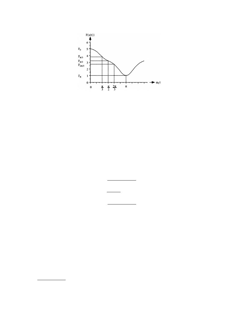
Three-Point Method
The three-point method is a simplified analysis applicable to small levels of distortion and can only be used to
calculate HD
2
. The output is written directly as a Fourier cosine series as in Eq. (5.3) where only terms up to
the second harmonic are retained. The dc component includes the quiescent state and the contribution due to
distortion that results in a shift of the dc operating point. The output waveform values at
w
1
t = 0 (F
0
),
w
1
t =
p/2 (F
p/2
),
w
1
t =
p (F
p
), as shown in
, are used to calculate Y
0
, Y
1
, and Y
2
.
(5.15)
The second harmonic distortion is calculated from the definition. From
, F
0
= 5, F
p/2
= 3.2, F
p
= 1, Y
0
= 3.1, Y
1
= 2.0, Y
2
= –0.1, and HD
2
= 5.0%.
Five-Point Method
The five-point method is an extension of the above technique and allows calculation of third and fourth
harmonic distortion factors. For distortion calculation the output is expressed as a Fourier cosine series with
terms up to the fourth harmonic where the dc component includes the quiescent state and the shift due to
distortion. The output waveform values at
w
1
t = 0 (F
0
),
w
1
t =
p/3 (F
p/3
),
w
1
t =
p/2 (F
p/2
),
w
1
t = 2
p/3 (F
2
p/3
),
w
1
t =
p (F
p
), as shown in Fig. 5.20, are used to calculate Y
0
, Y
1
, Y
2
, Y
3
, and Y
4
.
FIGURE 5.20
Output waveform from a nonlinear circuit.
Y
F
F
F
Y
F
F
Y
F
F
F
0
0
2
1
0
2
0
2
2
4
2
2
4
=
+
+
=
=
+
p
p
p
p
p
/
/
–
–

© 2000 by CRC Press LLC
(5.16)
For F
0
= 5,
F
p/3
= 3.8, F
p/2
= 3.2, F
2
p/3
= 2.7, F
p
= 1, Y
0
= 3.17, Y
1
= 1.7, Y
2
= –0.1, Y
3
= 0.3, Y
4
= –0.07, and
HD
2
= 5.9%, HD
3
= 17.6%. This particular method allows calculation of HD
3
and also gives a better estimate
of HD
2
. To obtain higher-order harmonics a detailed Fourier series analysis is required and for such applications
a circuit simulator, such as SPICE, should be used.
Intermodulation Distortion
The previous sections have examined the effect of nonlinear device characteristics when a single-frequency
sinusoidal signal is applied at the input. However, if there are two or more sinusoidal inputs, then the nonlin-
earity results in not only the fundamental and harmonics but also additional frequencies called the beat
frequencies at the output. The distortion due to the components at the beat frequencies is called
. To characterize this type of distortion consider the incremental output given by Eq. (5.10) and the
input signal to be
x(t) = X
1
cos
w
1
t + X
2
cos
w
2
t (5.17)
where f
1
=
w
1
/2
p and f
2
=
w
2
/2
p are the two input frequencies. The output frequency spectrum due to the
quadratic term is shown in
In addition to the dc term and the second harmonics of the two frequencies, there are additional terms at
the sum and difference frequencies, f
1
+ f
2
, f
1
– f
2
, which are the beat frequencies. The second-order intermod-
ulation distortion (IM
2
) is defined as the ratio of the amplitude at a beat frequency to the amplitude of the
fundamental component.
(5.18)
where it has been assumed that the contribution to second-order intermodulation by higher-order terms is
negligible. In defining IM
2
the input signals are assumed to be of equal amplitude and for this particular
condition IM
2
= 2 HD
2
[Eq. (5.12)].
TABLE 5.1
Output Frequency Spectrum Due to the Quadratic Term
Y
F
F
F
F
Y
F
F
F
F
Y
F
F
F
Y
F
F
F
F
Y
F
F
F
F
F
0
0
3
2
3
1
0
3
2
3
2
0
2
3
0
3
2
3
4
0
3
2
2
3
2
2
6
3
2
4
2
2
6
4
6
4
12
=
+
+
+
=
+
=
+
=
+
=
+
+
p
p
p
p
p
p
p
p
p
p
p
p
p
p
p
/
/
/
/
/
/
/
/
/
/
–
–
–
–
–
–
–
IM
2
2
1
2
1
1
2
2
1
=
=
a X X
a X
a X
a
Frequency
Amplitude
0
2
2
2
2
2
1
2
1
2
2
1
2
2
2 2
1
2 2
2
2
2
1
2
f
f
f
f
a
X
X
a
X
a
X
a X X
±
+
[
]
© 2000 by CRC Press LLC
The cubic term of the series expansion for the nonlinear circuit gives rise to components at frequencies 2f
1
+
f
2
, 2f
2
+ f
1
, 2f
1
– f
2
, 2f
2
– f
1
, and these terms result in third-order intermodulation distortion (IM
3
). The frequency
spectrum obtained from the cubic term is shown in
For definition purposes the two input signals are assumed to be of equal amplitude and IM
3
is given by
(assuming negligible contribution to the fundamental by the cubic term)
(5.19)
Under these conditions IM
3
= 3 HD
3
[Eq. (5.12)]. When f
1
and f
2
are close to one another, then the third-order
intermodulation components, 2f
1
– f
2
, 2f
2
– f
1
, are close to the fundamental and are difficult to filter out.
Triple-Beat Distortion
When three sinusoidal signals are applied at the input then the output consists of components at the triple-
beat frequencies. The cubic term in the nonlinearity results in the triple-beat terms
(5.20)
and the triple-beat distortion factor (TB) is defined for equal amplitude input signals.
(5.21)
From the above definition TB = 2 IM
3
. If all of the frequencies are close to one another, the triple beats will
be close to the fundamental and cannot be easily removed.
Cross Modulation
Another form of distortion that occurs in amplitude-modulated (AM) systems (Chapter 63) due to the circuit
nonlinearity is
. The modulation from an unwanted AM signal is transferred to the signal of
interest and results in distortion. Consider an AM signal
x(t) = X
1
cos
w
1
t + X
2
[1 + m cos
w
m
t]cos
w
2
t (5.22)
where m < 1 is the modulation index. Due to the cubic term of the nonlinearity the modulation from the
second signal is transferred to the first and the modulated component corresponding to the fundamental is
(5.23)
TABLE 5.2
Output Frequency Spectrum Due to the Cubic Term
Frequency
Amplitude
1
f
f
f
f
f
f
f
f
a
X
X X
a
X
X X
a X X
a X X
a X
a X
2
1
2
2
1
1
2
3
1
3
1
2
2 3
2
3
1
2
2
3
1
2
2
3
1
2
2
3
1
3
3
2
3
2
2
3
3
3
4
3
4
3
4
3
4
1
4
1
4
±
±
+
+
[
]
[
]
IM
3
3
1
3
1
1
3
1
2
1
3
4
3
4
=
=
a X
a X
a X
a
3
2
3
1
2
2
1
2
3
a X X X t
cos[ ]
w
w
w
±
±
TB
=
3
2
3
1
2
1
a X
a
a X
a X m
a
t
t
m
1
1
3
2
2
1
1
1
3
+
é
ë
ê
ê
ù
û
ú
ú
cos cos
w
w

© 2000 by CRC Press LLC
The cross-modulation factor (CM) is defined as the ratio of the transferred modulation index to the original
modulation.
(5.24)
The cross modulation is a factor of four larger than IM
3
and twelve times as large as HD
3
.
Compression and Intercept Points
For high-frequency circuits distortion is specified in terms of
compression and intercept points
. These quantities
are derived from extrapolated small-signal output power levels. The 1 dB compression point is defined as the
value of the fundamental output power for which the power is 1 dB below the extrapolated small-signal value.
The nth-order intercept point (IP
n
), n
³ 2, is the output power at which the extrapolated small-signal powers
of the fundamental and the nth harmonic intersect. Let P
in
be an input power that is small enough to ensure
small-signal operation. If P
1
is the output power of the fundamental, and P
n
the output power of the nth
harmonic, then the nth-order intercept point is given by IP
n
=
, where power is measured in dB.
Crossover Distortion
This type of distortion occurs in circuits that use devices operating in a “push-pull” manner. The devices are
used in pairs and each device operates only for half a cycle of the input signal (Class AB operation). One
advantage of such an arrangement is the cancellation of even harmonic terms resulting in smaller total harmonic
distortion. However, if the circuit is not designed to achieve a smooth crossover or transition from one device
to another, then there is a region of the transfer characteristics when the output is zero. The resulting distortion
is called
Failure-to-Follow Distortion
When a properly designed peak detector circuit is used for AM demodulation the output follows the envelope
of the input signal whereby the original modulation signal is recovered. A simple peak detector is a diode in
series with a low-pass RC filter. The critical component of such a circuit is a linear element, the filter capacitance
C. If C is large, then the output fails to follow the envelope of the input signal, resulting in
Frequency Distortion
Ideally an amplifier circuit should provide the same amplification for all input frequencies. However, due to
the presence of energy storage elements the gain of the amplifier is frequency dependent. Consequently different
frequency components have different amplifications resulting in
. The distortion is spec-
ified by a frequency response curve in which the amplifier output is plotted as a function of frequency. An ideal
amplifier has a flat frequency response over the frequency range of interest.
Phase Distortion
When the phase shift (
q) in the output signal of an amplifier is not proportional to the frequency, the output
does not preserve the form of the input signal, resulting in
. If the phase shift is proportional
to frequency, different frequency components have a constant delay time (
q/w) and no distortion is observed.
In TV applications phase distortion can result in a smeared picture.
Computer Simulation of Distortion Components
Distortion characterization is important for nonlinear circuits. However, the techniques presented for distortion
calculation can only be used for simple circuit configurations and at best to determine the second and third
CM
= 3
3
2
2
1
a X
a
nP P
n
n
1
1
-
-
© 2000 by CRC Press LLC
harmonic distortion factors. In order to determine the distortion generation in actual circuits one must fabricate
the circuit and then use a harmonic analyzer for sine curve inputs to determine the harmonics present in the
output. An attractive alternative is the use of circuit simulation programs that allow one to investigate circuit
performance before fabricating the circuit. In this section a brief overview of the techniques used in circuit
simulators for distortion characterization is provided.
The simplest approach is to simulate the time-domain output for a circuit with a specified sinusoidal input
signal and then perform a Fourier analysis of the output waveform. The simulation program SPICE2 provides
a capability for computing the Fourier components of any waveform using a .FOUR command and specifying
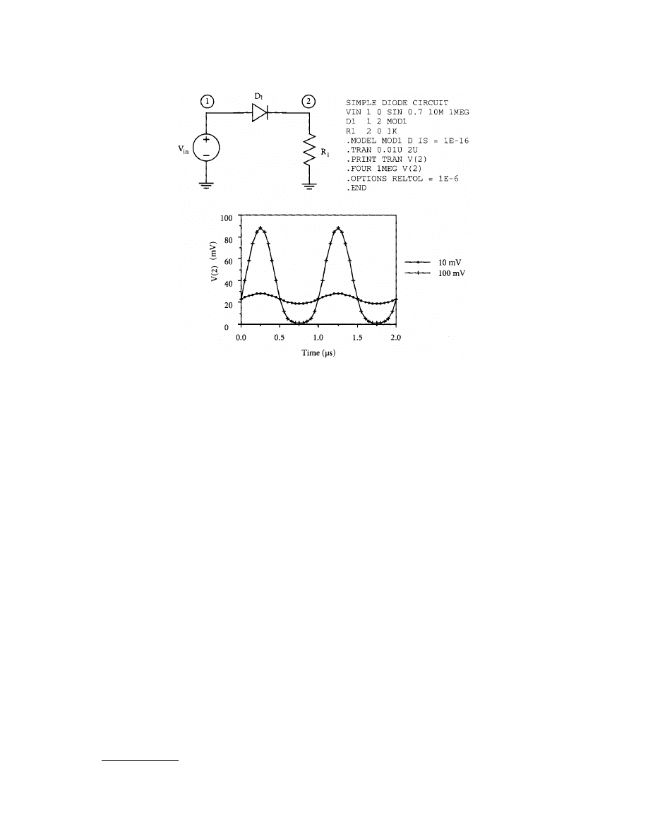
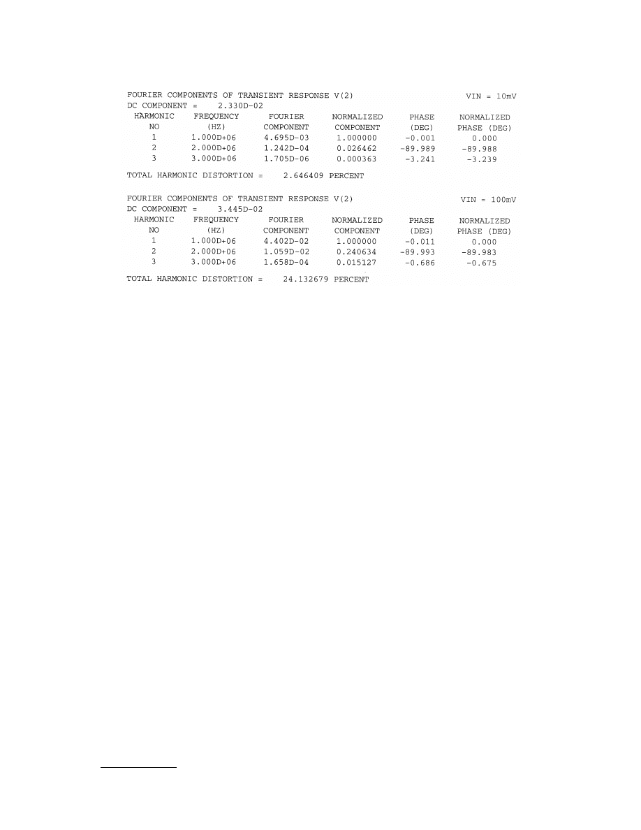
the voltage or current for which the analysis has to be performed. A simple diode circuit, the SPICE input file,
and transient voltage waveforms for an input signal frequency of 1 MHz and amplitudes of 10 and 100 mV
are shown in
. The Fourier components of the resistor voltage are shown in
fundamental and first two significant harmonics are shown (SPICE provides information to the ninth
harmonic).
In this particular example the input signal frequency is 1 MHz, and this is the frequency at which the Fourier
analysis is requested. Since there are no energy storage elements in the circuit another frequency would have
given identical results. To determine the Fourier components accurately a small value of the parameter RELTOL
is used and a sufficient number of points for transient analysis are specified. From the output voltage waveforms
and the Fourier analysis it is seen that the harmonic distortion increases significantly when the input voltage
amplitude is increased from 10 mV to 100 mV.
The transient approach can be computationally expensive for circuits that reach their periodic steady state
after a long simulation time. Results from the Fourier analysis are meaningful only in the periodic steady state,
and although this approach works well for large levels of distortion it is inaccurate for small distortion levels.
For small distortion levels accurate distortion analysis can be performed by use of the Volterra series method.
This technique is a generalization of the power-series method and is useful for analyzing harmonic and
intermodulation distortion due to frequency-dependent nonlinearities. The SPICE3 program supports this
analysis technique (in addition to the Fourier analysis of SPICE2) whereby the second and third harmonic and
intermodulation components can be efficiently obtained by three small-signal analyses of the circuit.
FIGURE 5.21
Simple diode circuit, SPICE input file, and output voltage waveforms.
© 2000 by CRC Press LLC
An approach based on the harmonic balance technique available in the simulation program SPECTRE is
applicable to both large and small levels of distortion. The program determines the periodic steady state of a
circuit with a sinusoidal input. The unknowns are the magnitudes of the circuit variables at the fundamental
frequency and at all the significant harmonics of the fundamental. The distortion levels can be simply calculated
by taking the ratios of the magnitudes of the appropriate harmonics to the fundamental.
Defining Terms
Compression and Intercept Points:
Characterize distortion in high-frequency circuits. These quantities are
derived from extrapolated small-signal output power levels.
Cross modulation:
Occurs in amplitude-modulated systems when the modulation of one signal is transferred
to another by the nonlinearity of the system.
Crossover distortion:
Present in circuits that use devices operating in a push-pull arrangement such that one
device conducts when the other is off. Crossover distortion results if the transition or crossover from
one device to the other is not smooth.
Failure-to-follow distortion:
Can occur during demodulation of an amplitude-modulated signal by a peak
detector circuit. If the capacitance of the low-pass RC filter of the peak detector is large, then the output
fails to follow the envelope of the input signal, resulting in failure-to-follow distortion.
Frequency distortion:
Caused by the presence of energy storage elements in an amplifier circuit. Different
frequency components have different amplifications, resulting in frequency distortion and the distortion
is specified by a frequency response curve.
Harmonic distortion:
Caused by the nonlinear transfer characteristics of a device or circuit. When a sinu-
soidal signal of a single frequency (the fundamental frequency) is applied at the input of a nonlinear
circuit, the output contains frequency components that are integer multiples of the fundamental fre-
quency (harmonics). The resulting distortion is called harmonic distortion.
Harmonic distortion factors:
A measure of the harmonic content of the output. The nth harmonic distortion
factor is the ratio of the amplitude of the nth harmonic to the amplitude of the fundamental component
of the output.
FIGURE 5.22
Fourier components of the resistor voltage for input amplitudes of 10 and 100 mV, respectively.

© 2000 by CRC Press LLC
Intermodulation distortion:
Distortion caused by the mixing or beating of two or more sinusoidal inputs
due to the nonlinearity of a device. The output contains terms at the sum and difference frequencies
called the beat frequencies.
Phase distortion:
Occurs when the phase shift in the output signal of an amplifier is not proportional to the
frequency.
Total harmonic distortion:
The ratio of the root-mean-square value of the harmonics to the amplitude of
the fundamental component of a waveform.
Related Topics
13.1 Analog Circuit Simulation • 47.5 Distortion and Second-Order Effects • 62.1 Power Quality Disturbances
References
K.K. Clarke and D.T. Hess, Communication Circuits: Analysis and Design, Reading, Mass.: Addison-Wesley, 1971.
P.R. Gray and R.G. Meyer, Analysis and Design of Analog Integrated Circuits, New York: John Wiley and Sons,
1992.
K.S. Kundert, Spectre User’s Guide: A Frequency Domain Simulator for Nonlinear Circuits, EECS Industrial Liaison
Program Office, University of California, Berkeley, 1987.
K.S. Kundert, The Designer’s Guide to SPICE and SPECTRE, Mass.: Kluwer Academic Publishers, 1995.
L.W. Nagel, “SPICE2: A Computer Program to Simulate Semiconductor Circuits,” Memo No. ERL-M520,
Electronics Research Laboratory, University of California, Berkeley, 1975.
D.O. Pederson and K. Mayaram, Analog Integrated Circuits for Communication: Principles, Simulation and Design,
Boston: Kluwer Academic Publishers, 1991.
T.L. Quarles, SPICE3C.1 User’s Guide, EECS Industrial Liaison Program Office, University of California, Ber-
keley, 1989.
J.S. Roychowdhury, “SPICE 3 Distortion Analysis,” Memo No. UCB/ERL M89/48, Electronics Research Labo-
ratory, University of California, Berkeley, 1989.
D.D. Weiner and J.F. Spina, Sinusoidal Analysis and Modeling of Weakly Nonlinear Circuits, New York: Van
Nostrand Reinhold Company, 1980.
Further Information
Characterization and simulation of distortion in a wide variety of electronic circuits (with and without feedback)
is presented in detail in Pederson and Mayaram [1991]. Also derivations for the simple analysis techniques are
provided and verified using SPICE2 simulations. Algorithms for computer-aided analysis of distortion are
available in Weiner and Spina [1980], Nagel [1975], Roychowdhury [1989], and Kundert [1987]. Chapter 5 of
Kundert [1995] gives valuable information on use of Fourier analysis in SPICE for distortion calculation in
circuits. The software packages SPICE2, SPICE3 and SPECTRE are available from EECS Industrial Liaison
Program Office, University of California, Berkeley, CA 94720.
5.4
Communicating with Chaos
Michael Peter Kennedy and Géza Kolumbán
The goal of a digital communications system is to deliver information represented by a sequence of binary
symbols from a transmitter, through a physical channel, to a receiver. The mapping of these symbols into analog
signals is called digital modulation.
In a conventional digital modulation scheme, the modulator represents each symbol to be transmitted as a
weighted sum of a number of periodic basis functions. For example, two orthogonal signals, such as a sine and
a cosine, can be used. Each symbol represents a certain bit sequence and is mapped to a corresponding set of
weights. The objective of the receiver is to recover the weights associated with the received signal and thereby

© 2000 by CRC Press LLC
to decide which symbol was transmitted [1]. The receiver’s estimate of the transmitted symbol is mapped back
to a bit sequence by a decoder.
When sinusoidal basis functions are used, the modulated signal consists of segments of periodic waveforms
corresponding to the individual symbols. A unique segment of analog waveform corresponds to each symbol.
If the spread spectrum technique is not used, the transmitted signal is narrow-band. Consequently, multipath
propagation can cause high attenuation or even dropout of the transmitted narrow-band signal.
Chaotic signals are nonperiodic waveforms, generated by deterministic systems, which are characterized by a
continuous “noise-like” broad power spectrum [2]. In the time domain, chaotic signals appear “random.” Chaotic
systems are characterized by “sensitive dependence on initial conditions”; an arbitrarily small perturbation even-
tually causes a large change in the state of the system. Equivalently, chaotic signals decorrelate rapidly with
themselves. The autocorrelation function of a chaotic signal has a large peak at zero and decays rapidly.
Thus, while chaotic signals share many of the properties of stochastic processes, they also possess a deter-
ministic structure that makes it possible to generate noise-like chaotic signals in a theoretically reproducible
manner. In particular, a continuous-time chaotic system can be used to generate a wideband noise-like signal
with robust and reproducible statistical properties [2].
Due to its wide-band nature, a signal comprising chaotic basis functions is potentially more resistant to
multipath propagation than one constructed of sinusoids. Thus,
where the digital
information signal to be transmitted is mapped to chaotic waveforms, is potentially useful in propagation
environments where multipath effects dominate.
In this chapter section, four chaotic digital modulation techniques are described in detail: Chaos Shift Keying
Differential Chaos Shift Keying
(DCSK), and FM-DCSK.
Elements of Chaotic Digital Communications Systems
In a digital communications system, the symbol to be transmitted is mapped by the modulator to an analog
sample function and this analog signal passes through an analog channel. The analog signal in the channel is
subject to a number of disturbing influences, including attenuation, bandpass filtering, and additive noise. The
role of the demodulator is to decide, on the basis of the received corrupted sample function, which symbol
was transmitted.
Transmitter
The sample function of duration T representing a symbol i is a weighted sum of analog basis functions g
j
(t):
(5.25)
In a conventional digital modulation scheme, the analog sample function of duration T that represents a
symbol is a linear combination of periodic, orthogonal basis functions (e.g., a sine and a cosine, or sinusoids at
different frequencies), and the symbol duration T is an integer multiple of the period of the basis functions.
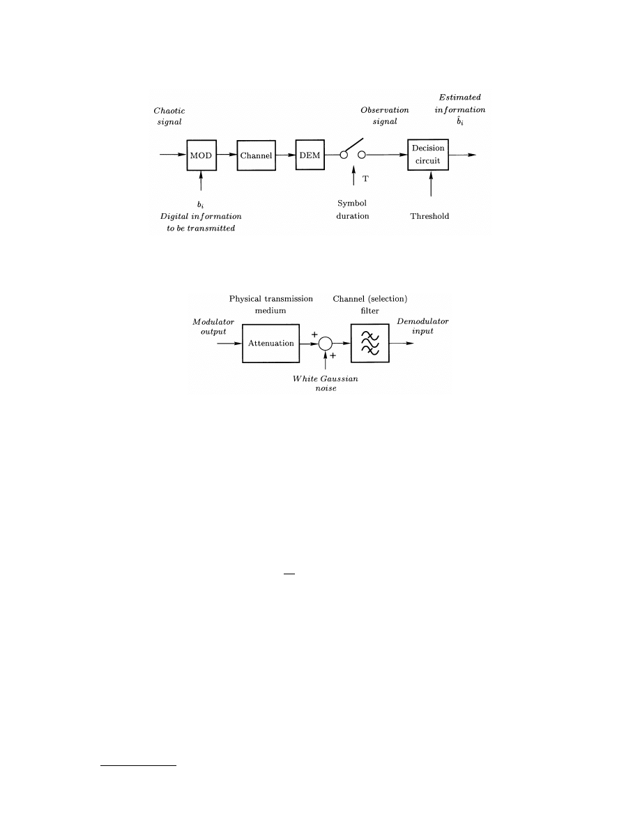
In a chaotic digital communications system, shown schematically in
, the analog sample function of
duration T that represents a symbol is a weighted sum of inherently nonperiodic chaotic basis function(s).
Channel Model
In any practical communications system, the signal r
i
(t) that is present at the input to the demodulator differs
from that which was transmitted, due to the effects of the channel.
The simplest realistic model of the channel is a linear bandpass channel with additive white Gaussian noise
(AWGN). A block diagram of the bandpass AWGN channel model that is considered throughout this section
and the next is shown in
. The additive noise is characterized by its power spectral density No.
Receiver
The role of the receiver in a digital communications system is to decide, on the basis of the received signal r
i
(t),
which symbol was transmitted. This decision is made by estimating some property of the received sample
s t
s g t
i
ij
j
j
N
( )
=
( )
=
∑
1
© 2000 by CRC Press LLC
function. The property, for example, could be the weights of the coefficients of the basis functions, the energy
of the received signal, or the correlation measured between different parts of the transmitted signal.
If the basis functions g
j
(t) are chosen such that they are periodic and orthogonal — that is:
(5.26)
then the coefficients s
ij
for symbol s
i
can be recovered in the receiver by evaluating the observation signals
(5.27)
Clearly, if r
i
(t) = s
i
(t), then z
ij
= s
ij
for every j, and the transmitted symbol can be identified.
In every physical implementation of a digital communications system, the received signal is corrupted by
noise and the observation signal becomes a random process. The decision rule is very simple: decide in favor
of the symbol to which the observation signal is closest.
Unlike periodic waveforms, chaotic basis functions are inherently nonperiodic and are different in each interval
of duration T. Chaotic basis functions have the advantage that each transmitted symbol is represented by a
unique analog sample function, and the correlation between chaotic sample functions is extremely low. How-
ever, it also produces a problem associated with estimating long-term statistics of a chaotic process from sample
functions of finite duration.
This is the so-called estimation problem, discussed next [3]. It arises in all chaotic digital modulation schemes
where the energy associated with a transmitted symbol is different every time that symbol is transmitted.
FIGURE 5.23
Block diagram of a chaotic communications scheme. The modulator and demodulator are labeled MOD
and DEM, respectively.
FIGURE 5.24
Model of an additive white Gaussian noise channel including the frequency selectivity of the receiver.
g t g t dt
K
i
j
i
j
T
( ) ( )
=
=
∫
if
otherwise
0
z
K
r t g t dt
ij
i
j
T
=
( ) ( )
∫
1
© 2000 by CRC Press LLC
The Estimation Problem
In modulation schemes that use periodic basis functions, s
i
(t) is periodic and the bit duration T is an integer
multiple of the period of the basis function(s); hence,
∫
T
s
i
2
(t)dt is constant. By contrast, chaotic signals are
inherently nonperiodic, so
∫
T
s
i
2
(t)dt varies from one sample function of length T to the next.
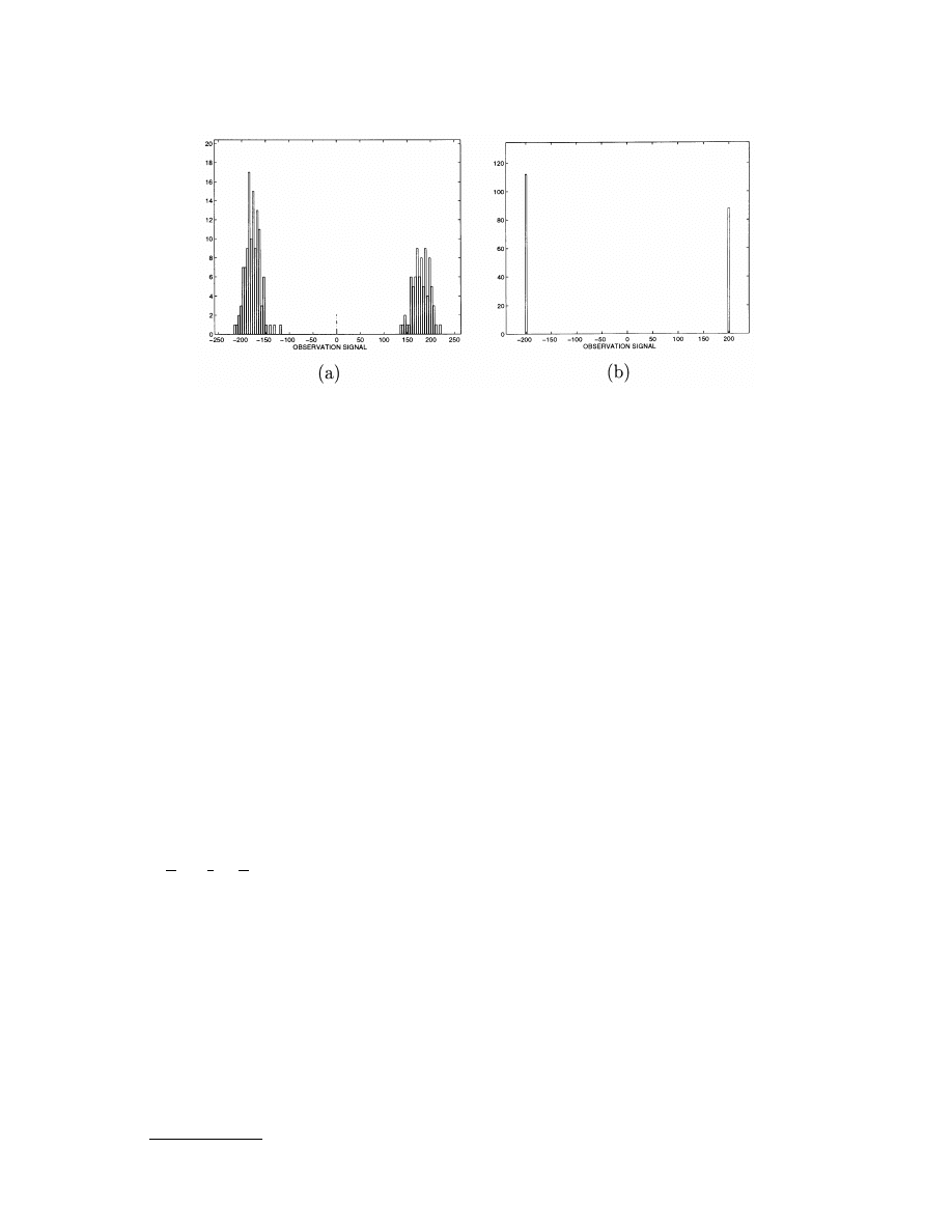
This effect is illustrated in
, which shows a histogram of the observation signal in a noise-free
binary
scheme where s
i1
(t) = g(t) and s
i2
(t) = –g(t). The observation signal is given by
(5.28)
Because the basis function g(·) is not periodic, the value
∫
T
g
2
(t)dt varies from one symbol period of length
T to the next. Consequently, the samples of the observation signal z
i
corresponding to symbols “0” and “1” are
clustered with non-zero variance about –180 and +180, respectively. Thus, the nonperiodic nature of the chaotic
signal itself produces an effect that is indistinguishable at the receiver from the effect of additive channel noise.
By increasing the bit duration T, the variance of estimation can be reduced, but it also imposes a constraint on
the maximum symbol rate. The estimation problem can be solved completely by keeping the energy per symbol
constant. In this case, the variance of the samples of the observation signal is zero, as shown in
Chaotic Digital Modulation Schemes
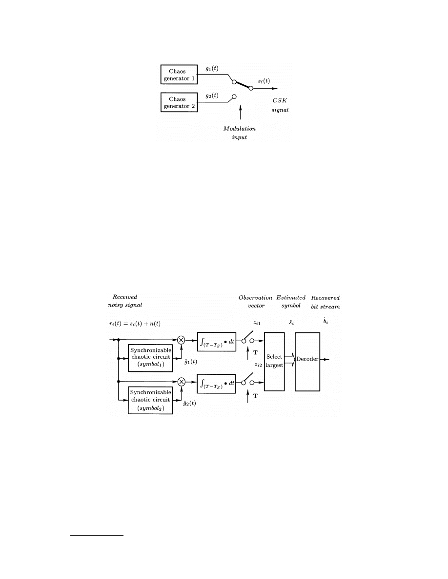
In Chaos Shift Keying (CSK), each symbol is represented by a weighted sum of chaotic basis functions g
j
(t). A
binary CSK transmitter is shown in
. The sample function s
i
(t) is g
1
(t) or g
2
(t), depending on whether
symbol “1” or “0” is to be transmitted.
The required chaotic basis functions can be generated by different chaotic circuits (as shown in
or they can be produced by a single chaotic generator whose output is multiplied by two different constants.
In both cases, the binary information to be transmitted is mapped to the bit energies of chaotic sample functions.
In chaotic digital communications systems, as in conventional communications schemes, the transmitted
symbols can be recovered using either coherent or noncoherent demodulation techniques.
Coherent Demodulation of CSK
Coherent demodulation is accomplished by reproducing copies of the basis functions in the receiver, typically
by means of a synchronization scheme [4]. When synchronization is exploited, the synchronization scheme
must be able to recover the basis function(s) from the corrupted received signal.
FIGURE 5.25
Histograms of the observation signal z
i
for (a) non-constant and (b) constant energy per symbol.
z
g t dt
i
g t dt
i
i
T
T
=
+
( )
−
( )
∫
∫
2
2
when symbol is 1
when symbol is 0
" "
" "
© 2000 by CRC Press LLC
If a single sinusoidal basis function is used, then a narrow-band phase-locked loop (PLL) can be used to
recover it [1]. Noise corrupting the transmitted signal is suppressed because of the low-pass property of the
PLL. When an inherently wideband chaotic basis function is used, the synchronized circuit must also be
wideband in nature. Typically, both the “amplitude” and “phase” of the chaotic basis function must be recovered
from the received signal. Because of the wideband property of the chaotic basis function, narrow-band linear
filtering cannot be used to suppress the additive channel noise.
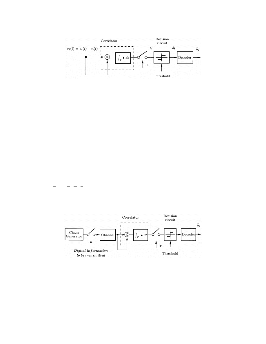
Figure 5.27 shows a coherent (synchronization-based) receiver using binary CSK modulation with two basis
functions g
1
(t) and g
2
(t). Synchronization circuits at the receiver attempt to reproduce the basis functions, given
the received noisy sample function r
i
(t) = s
i
(t) + n(t).
An acquisition time T
S
is allowed for the synchronization circuits to lock to the incoming signal. The recovered
basis functions ˆg
1
(t) and ˆg
2
(t) are then correlated with r
i
(t) for the remainder of the bit duration T. A decision
is made on the basis of the relative closeness of r
i
(t) to ˆg
1
(t) and ˆg
2
(t), as quantified by the observation variables
z
i1
and z
i2
, respectively.
where significant noise and filtering have been introduced in the channel,
suggest that the performance of chaotic synchronization schemes is significantly worse at low signal-to-noise
ratio (SNR) than that of the best synchronization schemes for sinusoids [4–6].
Noncoherent Demodulation of CSK
Synchronization (in the sense of carrier recovery) is not a necessary requirement for digital communications;
demodulation can also be performed without synchronization. This is true for both periodic and chaotic sample
functions.
FIGURE 5.26
Block diagram of a CSK modulator.
FIGURE 5.27
Block diagram of a coherent CSK receiver.
© 2000 by CRC Press LLC
Due to the nonperiodic property of chaotic signals, the energy of chaotic sample functions varies from one
sample function to the next, even if the same symbol is transmitted. If the mean bit energies
∫
T
g
1
2
(t)dt and
∫
T
g
2
2
(t)dt associated with symbols “1” and “0,” respectively, are sufficiently different, then a CSK transmission
can be demodulated without synchronization. In this case, the bit energy can be estimated by a correlator at
the receiver, as shown in
, without recovering the basis functions. The decision as to which symbol
was transmitted is made by comparing this estimate against a threshold.
The observation signal z
i
that is used by the decision circuit is defined by
(5.29)
where
∫
T
denotes integration over one bit period.
For a given noise level and chaotic signal, the best noise performance of CSK can be achieved if the distance
between the mean bit energies of the two symbols is maximized; this requirement can be satisfied by the Chaotic
On-Off Keying technique, described next.
Chaotic On-Off Keying (COOK)
In the Chaotic On-Off Keying (COOK) scheme, the chaotic signal is switched on and off to transmit symbols
“1” and “0,” respectively, as shown in
If the average bit energy is E
b
and both symbols are equiprobable, then the distance between the elements
of the signal set is 2E
b
. It is well-known from the theory of communications systems that the greater the distance
between the elements of the signal set, the better the noise performance of a modulation scheme [1]. The noise
performance of COOK represents the upper bound for CSK because the distance between the elements of the
signal set is maximized.
Notice that the observation signal is determined by the energy per bit of the noisy received signal r
i
(t) =
s
i
(t) + n(t). This is why a significant drawback of the CSK system — namely that the threshold value of the
decision circuit depends on the noise level — also applies to COOK. This means that using COOK, one can
maximize the distance between the elements of the signal set, but the threshold level required by the decision
FIGURE 5.28
Block diagram of a non-coherent CSK receiver.
FIGURE 5.29
Block diagram of COOK modulation scheme with non-coherent demodulation.
z
r
t dt
i
i
T
=
( )
∫
2
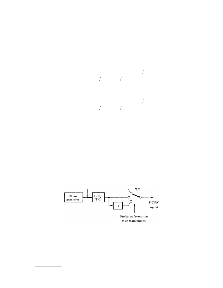
© 2000 by CRC Press LLC
circuit depends on the SNR. The threshold can be kept constant by applying the Differential Chaos Shift Keying
method.
Differential Chaos Shift Keying (DCSK)
In Differential Chaos Shift Keying (DCSK), every symbol to be transmitted is represented by two chaotic sample
functions. The first sample function serves as a reference, while the second one carries the information. symbol
“1” is sent by transmitting a reference signal provided by a chaos generator twice in succession; while for symbol
“0,” the reference chaotic signal is transmitted, followed by an inverted copy of the same integral. Thus,
(5.30)
if symbol “1” is transmitted in (t
i
, t
i
+ T) and
(5.31)
if symbol “0” is transmitted in (t
i
, t
i
+ T).
Figures 5.30 and 5.31 show a block diagram of a DCSK modulator and a typical DCSK signal corresponding
to the binary sequence 1100. In this example, the chaotic signal is produced by an analog phase-locked loop
(APLL) and the bit duration is 20 ms.
Since each bit is mapped to the correlation between successive segments of the transmitted signal of length
T/2, the information signal can be recovered by a correlator. A block diagram of a DCSK demodulator is shown
in Fig. 5.32.
The received noisy signal is delayed by half of the bit duration (T/2), and the correlation between the received
signal and the delayed copy of itself is determined. The decision is made by a level comparator [7].
In contrast to the CSK and COOK schemes discussed above, DCSK is an antipodal modulation scheme. In
addition to superior noise performance, the decision threshold is zero independently of the SNR [7].
A further advantage results from the fact that the reference- and information-bearing sample functions pass
through the same channel, thereby rendering the modulation scheme insensitive to channel distortion. DCSK
can also operate over a time-varying channel if the parameters of the channel remain constant for half the bit
duration T.
The principal drawback of DCSK arises from the fact that the correlation is performed over half the bit
duration. Compared to conventional techniques where the elements of the signal set are available at the receiver,
DCSK has half of the data rate, and only half the bit energy contributes to its noise performance [4,6].
In the CSK, COOK, and DCSK modulation schemes, the information signal to be transmitted is mapped
to chaotic sample functions of finite length. The property required by the decision circuit at the receiver to
FIGURE 5.30
Block diagram of a DCSK modulator.
s t
x t
t
t
t
T
x t T
t
T
t
t
T
i
i
i
i
( )
=
( )
≤ < +
+
−
(
)
+
≤
< +
,
,
2
2
2
s t
x t
t
t
t
T
x t T
t
T
t
t
T
i
i
i
i
( )
=
( )
≤ < +
−
−
(
)
+
≤
< +
,
,
2
2
2
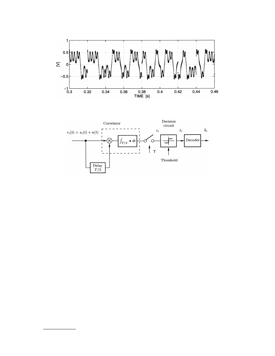
© 2000 by CRC Press LLC
perform the demodulation can only be estimated because of the nonperiodic nature of chaotic signals. The
estimation has a non-zero variance even in the noise-free case; this puts a lower bound on the bit duration and
thereby limits the data rate.
One way to improve the data rate is to use a multilevel modulation scheme such as those described in [8].
Alternatively, one can solve the estimation problem directly by modifying the modulation scheme such that
the transmitted energy for each symbol is kept constant. FM-DCSK is an example of the latter approach.
FM-DCSK
The power of a
(FM) signal is independent of the modulation. Therefore, if a chaotic
signal is applied to the input of an FM modulator, and the output of the FM modulator is applied to the input
of a DCSK modulator, then the resulting output of the DCSK modulator has constant energy per symbol. If
this signal is applied directly to a DCSK correlation receiver, then the observation signal in the receiver has
zero variance in the noise-free case and the estimation problem is solved.
As in the DCSK technique, every information bit is transmitted in two pieces: the first sample function serves
as a reference, while the second one carries the information. The operation of the modulator shown in Fig. 5.33
is similar to DCSK, the difference being that the FM signal, rather than the chaotic signal itself, is applied to
the input of the DCSK modulator. In this example, the chaotic signal is generated by an appropriately designed
analog phase-locked loop (APLL).
The demodulator of an FM-DCSK system is a DCSK receiver. The only difference is that, instead of low-
frequency chaotic signals, the noisy FM signals are correlated directly in the receiver, as shown in Fig. 5.34.
The noise performance of the FM-DCSK system is an attainable upper bound to that of DCSK. The main
advantage of FM-DCSK modulation over CSK, COOK, and DCSK is that the data rate is not limited by the
properties of the chaotic signal.
FIGURE 5.31
DCSK signal corresponding to binary sequence 1100.
FIGURE 5.32
Block diagram of a DCSK receiver.
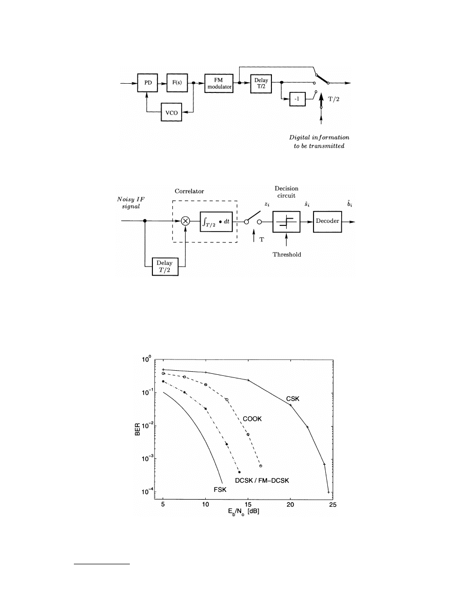
© 2000 by CRC Press LLC
Performance Evaluation
The noise performance of a digital modulation scheme is characterized by plotting the bit error rate (BER) as
a function of the ratio of the energy per bit to the noise spectial density. (E
b
/N
0
). The simulated noise perfor-
mance of noncoherent CSK, COOK, and DCSK/FM-DCSK is summarized graphically in Fig. 5.35.
FIGURE 5.33
Block diagram of an FM-DCSK modulator.
FIGURE 5.34
Block diagram of an FM-DCSK demodulator.
FIGURE 5.35
Noise performance of the CSK, COOK, and DCSK/FM-DCSK techniques. Non-coherent FSK is shown for
comparison.

© 2000 by CRC Press LLC
The upper bound on the data rate of DCSK can be increased by using multilevel modulation schemes or by
keeping the transmitted energy constant for each symbol. The FM-DCSK technique, which is an antipodal
modulation scheme with constant bit energy, represents an optimal solution in the sense that its noise perfor-
mance is equal to that of DCSK but the data rate is not limited by the properties of the underlying chaotic signal.
Low-Pass Equivalent Models for Chaotic Communications Systems
The previous sections have described
schemes. The output of these modulations is
generally a low-pass signal. Many telecommunications channels, such as a radio channel, can transmit only
bandpass signals, so a second modulation scheme must be used to produce an RF output in these cases. An
exception is the FM-DCSK modulation scheme, where the output of the FM modulator is already a bandpass
RF signal and the DCSK modulation is applied directly to this signal.
The performance evaluation of communications systems can be done analytically only in the simplest cases;
usually, computer simulation is required. However, if computer simulations of RF communications systems
are performed directly in the RF domain, then the sampling frequency for the simulation depends on both the
carrier frequency and the bandwidth of the transmitted signal. The high carrier frequency results in a high
sampling frequency and consequently a long simulation time. On the other hand, the parameters of a bandpass
system do not depend on the actual value of the carrier frequency.
It is well-known that a low-pass equivalent model can be developed for every bandpass system [1]. As a
result, the carrier frequency can be removed from the model of an RF communications system and the sampling
frequency is then determined solely by the bandwidth of the RF signal. This reduces significantly the compu-
tational effort required to characterize the performance of a chaotic communications system. This section
illustrates the development of a low-pass equivalent model for the RF FM-DCSK system. For further details
and models of other chaotic communications systems, see [9].
Theoretical Background
Representation of Bandpass Signals
A signal x(t) is referred to as a bandpass signal if its energy is nonnegligible only in a frequency band of total
extent 2BW centered about a carrier frequency f
c
. Every bandpass signal can be expressed in terms of a slowly
varying signal ˜x(t) and a complex exponential
(5.32)
where ˜x(t) is called the complex envelope, and
ω
c
= 2
π
f
c
. In general, ˜x(t) is a complex-valued quantity; it can
be expressed in terms of its in-phase and quadrature components, x
I
(t) and x
Q
(t), as follows:
(5.33)
Both x
I
(t) and x
Q
(t) are low-pass signals limited to the frequency band –BW
≤
f
≤
BW.
The complex envelope ˜x(t) carries all of the information, except the carrier frequency, of the original bandpass
signal x(t). This means that if the complex envelope of a signal is given, then that signal is completely characterized.
Knowing the carrier frequency, in addition, means that the original bandpass signal can be reconstructed.
The in-phase and quadrature components of the complex envelope can be generated from the bandpass
signal x(t) using the scheme shown in Fig. 5.36, where the ideal low-pass filters have bandwidth BW.
The original bandpass signal x(t) can be reconstructed from the in-phase and quadrature components of ˜x(t)
as shown in Fig. 5.37.
Representation of Bandpass Systems
Let the bandpass input signal x(t) be applied to a linear time-invariant bandpass system with impulse response
h(t), and let the bandwidth of the bandpass system be equal to 2B and centered about the carrier frequency f
c
.
Then, by analogy with the representation of bandpass signals, the impulse response of the bandpass system can
also be expressed in terms of a slowly varying complex impulse response ˜
h(t) and a complex exponential:
x t
x t e
j
t
c
( )
=
( )
[
]
Re ˜
ω
˜
x t
x t
j x t
I
Q
( )
=
( )
+
( )
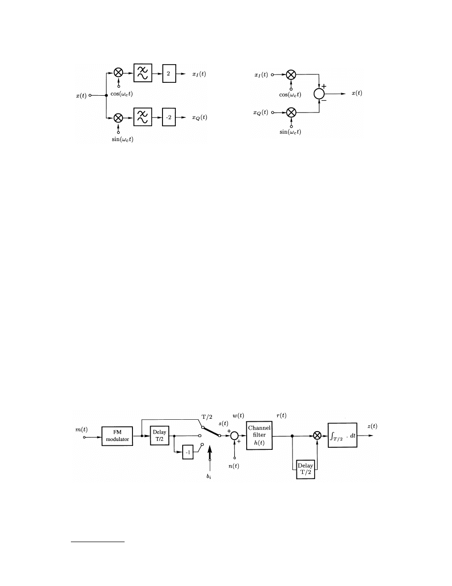
© 2000 by CRC Press LLC
(5.34)
In general, the complex impulse response is a complex-valued quantity that can be expressed in terms of its
in-phase and quadrature components
(5.35)
where ˜
h(t), h
I
(t), and h
Q
(t) are all low-pass functions limited to the frequency band –B
≤
f
≤
B.
Representation of Bandpass Gaussian Noise
If the channel noise n(t) is a bandpass Gaussian random process and its spectrum is symmetric about the
carrier frequency f
c
, then n(t) can also be represented by its complex envelope
(5.36)
Low-Pass Equivalent of FM-DCSK System
The block diagram of a general chaotic communications system is given in
the demodulator of an FM-DCSK system is a correlator, and the observation signal z
i
is the correlator output
sampled at the decision time instants. To derive the low-pass equivalent model of a chaotic communications
scheme, the relationship between the analog input and output signals must be found; that is, the correlator
output z(t) must be determined for a given analog input signal.
The block diagram of the RF FM-DCSK system to be transformed is shown in Fig. 5.38, where h(t) denotes
the impulse response of channel filter, n(t) is the channel noise, and w(t) is the input to the channel filter.
FIGURE 5.36
Generation of the in-phase and quad-
rature components of a bandpass signal.
FIGURE 5.37
Reconstruction of the original bandpass
signal from its in-phase and quadrature components.
FIGURE 5.38
Block diagram of an RF FM-DCSK system.
h t
h t e
j
t
c
( )
=
( )
[
]
Re ˜
ω
˜
h t
h t
jh t
I
Q
( )
=
( )
+
( )
˜
n t
n t
jn t
I
Q
( )
=
( )
+
( )
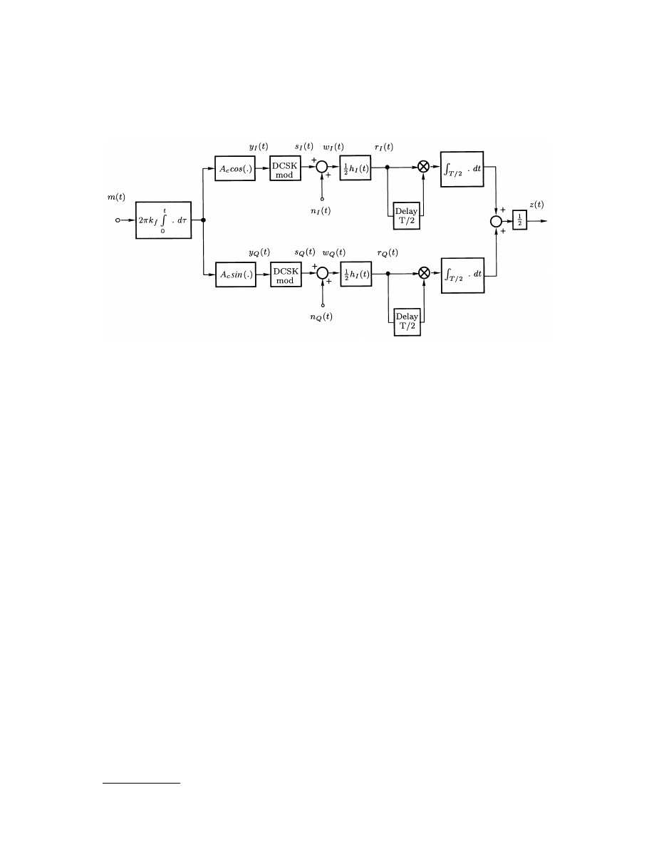
© 2000 by CRC Press LLC
Applying the theorems of the analytic signal approach [1], assuming a zero-phase channel filter and that
half of the bit duration is equal to an entire multiple of the RF carrier period, the low-pass equivalent model
of the RF FM-DCSK system can be developed as shown in Fig. 5.39 (for further details, see [9]).
Note that all RF signals and the carrier frequency have been removed from Fig. 5.39. Consequently, the
sampling frequency required for computer simulations is determined exclusively by the slowly-varying low-
pass signals. All noise performance curves shown in this chapter section have been determined using low-pass
equivalent models derived in this way.
Multipath Performance of FM-DCSK
In many applications, such as mobile communications or indoor radio, the transmitted signal arrives at the
receiver via multiple propagation paths with different delays, thus giving rise to multipath propagation. The
components arriving via different propagation paths may add destructively, resulting in deep frequency-selective
fading. Conventional narrow-band systems completely fail to operate if a multipath-related null (defined below)
resulting from deep frequency-selective fading coincides with the carrier frequency. Because of the inherently
broad-band nature of chaotic signals, chaotic modulation schemes have potentially better performance in
multipath environments than narrow-band ones. In this section, the performance degradation of the FM-DCSK
scheme resulting from multipath propagation is determined by computer simulation.
FIGURE 5.39
Low-pass equivalent model of the RF FM-DCSK chaotic communications system shown in Fig. 5.38.
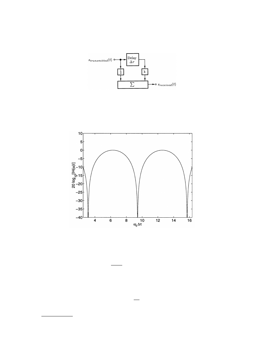
© 2000 by CRC Press LLC
Multipath Model
A time-invariant multipath radio channel having two propagation paths can be modeled as shown in Fig. 5.40.
In the worst case, the two received signals cancel each other completely at the carrier frequency
ω
c
; that is,
∆τω
c
= (2n + 1)
π
, n = 0,
±
1,
±
2,…, and k = –1/2, where
∆τ
denotes the additional delay of the second path.
Let the multipath channel be characterized by its frequency response shown in Fig. 5.41. Note that the
multipath-related nulls, where the attenuation becomes infinitely large, appear at
(5.37)
Let the bandwidth of fading be defined as the frequency range over which the attenuation of the multipath
channel is greater than 10 dB. Then the bandwidth of fading can be expressed as
(5.38)
FIGURE 5.40
Tapped delay line model of a multipath radio channel.
FIGURE 5.41
Magnitude of the frequency response of a multipath channel.
f
n
n
null
=
+
= ± ± …
2
1
2
0
1
2
∆τ
,
,
,
,
∆
∆
f
null
≈
0 1
.
τ
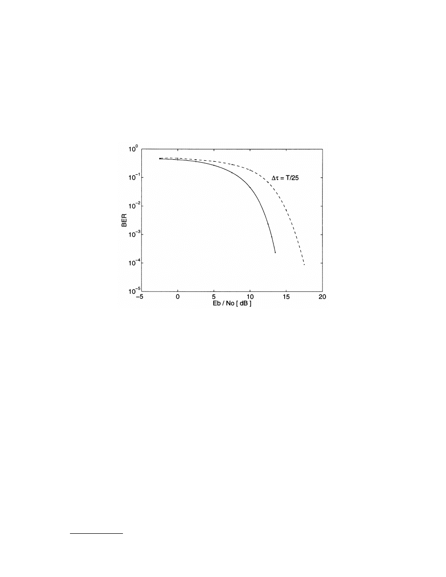
© 2000 by CRC Press LLC
Performance of FM-DCSK Modulation Scheme
Figure 5.41 shows why conventional narrow-band systems can fail to operate over a multipath channel. Due
to high attenuation appearing about the multipath-related nulls, the SNR becomes extremely low at the input
of the receiver. Consequently, the demodulator and the carrier recovery circuit, if used, cannot operate.
In a chaotic communications system, the power of the radiated signal is spread over a wide frequency range.
The appearance of a multipath-related null means that part of the transmitted power is lost, but the system
still operates. Of course, the lower SNR at the demodulator input results in a worse bit error rate.
The performance degradation of the FM-DCSK system due to multipath propagation is shown in Fig. 5.42,
where
∆τ
= T/25. The solid line shows the noise performance if multipath propagation is not present, while
the system performance for k = –1/2 is given by the dashed curve. Note that FM-DCSK performs extremely
well over a radio channel suffering from multipath effects; the performance degradation even in the worst case
is less than a few dB. Note that conventional narrow-band systems cannot operate over this channel.
Defining Terms
Chaotic synchronization:
The process by which a dynamical system is synchronized with a chaotic reference
signal. In chaotic digital communications, chaotic (rather than periodic) basis functions must be recov-
ered without distortion from the noisy received (reference) signal at the receiver. Noise corrupting the
reference signal must be suppressed as much as possible.
Chaotic digital modulation:
The mapping of information-source symbols into chaotic signals, which is
performed to carry information through the analog transmission channel.
Chaos shift keying:
A digital modulation scheme in which the source information is carried by the coefficients
of a weighted sum of chaotic waveforms.
Chaotic on-off keying:
A binary digital modulation scheme in which the chaotic carrier is switched on or
off, depending on the binary information to be transmitted.
Differential chaos shift keying:
A digital modulation scheme in which the source information is carried by
the correlation between segments of a chaotic waveform that are separated in time.
FIGURE 5.42
Noise performance of FM-DCSK with (dashed curve) and without (solid curve) multipath effects.

© 2000 by CRC Press LLC
Frequency-modulated differential chaos shift keying:
A digital modulation scheme in which the source
information is carried by the correlation between chaotic frequency-modulated waveforms.
References
1. S.S. Haykin. Communication Systems, 3rd edition, John Wiley & Sons, New York, 1994.
2. M.P. Kennedy. Bifurcation and chaos, in The Circuits and Filters Handbook, W.K. Chen, Editor, pages
1089–1164. CRC Press, 1995.
3. G. Kolumbán, M.P. Kennedy, and G. Kis. Determination of symbol duration in chaos-based communi-
cations, Proc. NDES’97, pages 217–222, Moscow, Russia, 26–27 June, 1997.
4. G. Kolumbán, M.P. Kennedy, and L.O. Chua. The role of synchronization in digital communications
using chaos. Part I. Fundamentals of digital communications. IEEE Trans. Circuits and Systems. Part I.
Fundamental Theory and Applications, 44(10):927–936, 1997.
5. G. Kolumbán, H. Dedieu, J. Schweizer, J. Ennitis, and B. Vizvári. Performance evaluation and comparison
of chaos communication systems, in Proc. NDES’96 pages 105–110, Sevilla, 27–28 June, 1996.
6. G. Kolumbán, M.P. Kennedy, and L.O. Chua. The role of synchronization in digital communications
using chaos. Part II. Chaotic modulation and chaotic synchronization, IEEE Trans. Circuits and Systems.
Part I. Fundamental Theory and Applications, 45(11):1129–1140, 1998.
7. G. Kolumbán, B. Vizvári, W. Schwarz, and A. Abel. Differential chaos shift keying: A robust coding for
chaotic communications, Proc. NDES’96, pages 87–92, Sevilla, 27–28 June, 1996.
8. G. Kolumbán, M.P. Kennedy, and G. Kis. Multilevel differential chaos shift keying, Proc. NDES’97, pages
191–196, Moscow, Russia, 26–27 June, 1997.
9. G. Kolumbán. Performance evaluation of chaotic communications systems: determination of low-pass
equivalent model, Proc. NDES’98, pages 41–51, Budapest, Hungary, 17–18 July, 1998.
10. R.C. Dixon. Spread Spectrum Communication Systems with Commercial Applications, 3rd edition, Wiley,
New York, 1994.
11. L.M. Pecora and T.L. Carroll. Synchronization in chaotic systems, Phys. Rev. Lett., 64(8):821–824, 1990.
12. M. Hasler. Engineering chaos for encryption and broadband communication, Phil. Trans. R. Soc. Lond.,
353(1701):115–126, 1995.
13. G. Kolumbán, G. Kis, Z. Jákó, and M.P. Kennedy. FM-DCSK: a robust modulation scheme for chaotic
communications, IEICE Transactions, E81-A(9): 1798–1802, September 1998.
14. G. Heidari-Bateni and C.D. McGillem. A chaotic direct sequence spread spectrum communication system,
IEEE Trans. Commun., COM-42(2/3/4):1524–1527, 1994.
15. N.F. Rulkov, M.M. Sushchik, L.S. Tsimring, and H.D. Abarbanel. Generalized synchronization of chaos
in directionally coupled chaotic systems, Phys. Rev. E., 51(2):980–994, 1995.
16. S. Hayes, C. Grebogi, and E. Ott. Communicating with chaos, Phys. Rev. Lett., 70(20):3031–3034, 1993.
Further Information
An introduction to chaos for electrical engineers can be found in [2].
Digital modulation theory and low-pass equivalent circuits of bandpass communications systems are
described at an introductory level in [1]. The theory of spread spectrum communications can be found in [10].
The field of communicating with chaos has developed rapidly since the experiments by Pecora, Carroll, and
others in the 1990s on chaotic synchronization [11]. Hasler [12] has written an overview of early work in this
field.
The role of synchronization in chaotic digital modulation is explored in [4,6]. These papers also describe
the state of the art in noncoherent receivers for chaotic digital communications. FM-DCSK is developed in [13].
Advances in the theory and practice of chaotic communications in electrical engineering are reported in
Electronics Letters, the IEEE Transactions on Circuits and Systems, and the IEEE Transactions on Communications.
This section has focused exclusively on chaotic modulation techniques. Other applications of chaotic signals
and synchronization schemes have been proposed but they are less close to practice: discrete-time chaotic
sequences for spread spectrum systems were introduced in [14]; synchronization techniques for chaotic systems,

such as [15] and methods for transmitting or hiding information (e.g., [16]), are frequently reported in physics
journals such as Physical Review Letters and the Physical Review E.
Document Outline
- Contents
- Nonlinear Circuits
- 5.1Diodes and Rectifiers
- 5.2Limiters
- 5.3Distortion
- Harmonic Distortion
- Power-Series Method
- Differential-Error Method
- Three-Point Method
- Five-Point Method
- Intermodulation Distortion
- Triple-Beat Distortion
- Cross Modulation
- Compression and Intercept Points
- Crossover Distortion
- Failure-to-Follow Distortion
- Frequency Distortion
- Phase Distortion
- Computer Simulation of Distortion Components
- 5.4 Communicating with Chaos
Wyszukiwarka
Podobne podstrony:
A Novel Switch mode DC to AC Inverter With Non linear Robust Control
Chang S Y A Non linear elliptic equations in conformal geometry (EMS, 2004)(ISBN 303719006X)(O)(100s
Linear and non Linear SR 2012
A Novel Switch Mode Dc To Ac Inverter With Non Linear Robust Control
A Comparison of Linear Vs Non Linear Models of Aversive Self Awareness, Dissociation, and Non Suicid
Non linear rheology of active particle suspensions
PP MEMS 06 Non linear Dynamics
77 Linear Circuits
Linearization of non linear state equation
A Novel Switch Mode Dc To Ac Inverter With Non Linear Robust Control(1)
78 Hormony wysp trzustki
WEM 1 78 Paradygmat
WEM 5 78 Prawidlowosci dot procesu emocjonalnego II
Neural networks in non Euclidean metric spaces
circuit cellar1995 06
78 pdfsam Raanan Gillon Etyka lekarska Problemy filozoficzne
Microwaves in organic synthesis Thermal and non thermal microwave
circuit cellar1996 11
więcej podobnych podstron