DG641/642/643
Siliconix
S-52880—Rev. D, 28-Apr-97
1
Low On-Resistance Wideband/Video Switches
Features
Benefits
Applications
Wide Bandwidth: 500 MHz
Low Crosstalk at 5 MHz: –85 dB
Low r
DS(on)
: 5
, DG642
TTL Logic Compatible
Fast Switching: t
ON
50 ns
Single Supply Compatibility
High Current: 100 mA, DG642
High Precision
Improved Frequency Response
Low Insertion Loss
Improved System Performance
Reduced Board Space
Low Power Consumption
RF and Video Switching
RGB Switching
Video Routing
Cellular Communications
ATE
Radar/FLIR Systems
Satellite Receivers
Programmable Filters
The DG641/642/643 are high performance monolithic
video switches designed for switching wide bandwidth
analog and digital signals. DG641 is a quad SPST, DG642
is a single SPDT, and DG643 is a dual SPDT function. These
devices have exceptionally low on-resistances (5
typ—DG642), low capacitance and high current handling
capability.
To achieve TTL compatibility, low channel capacitances
and fast switching times, the DG641/642/643 are built on
the Siliconix proprietary D/CMOS process. Each switch
conducts equally well in both directions when on, and
blocks up to 14 V
p-p
when off. An epitaxial layer prevents
latchup.
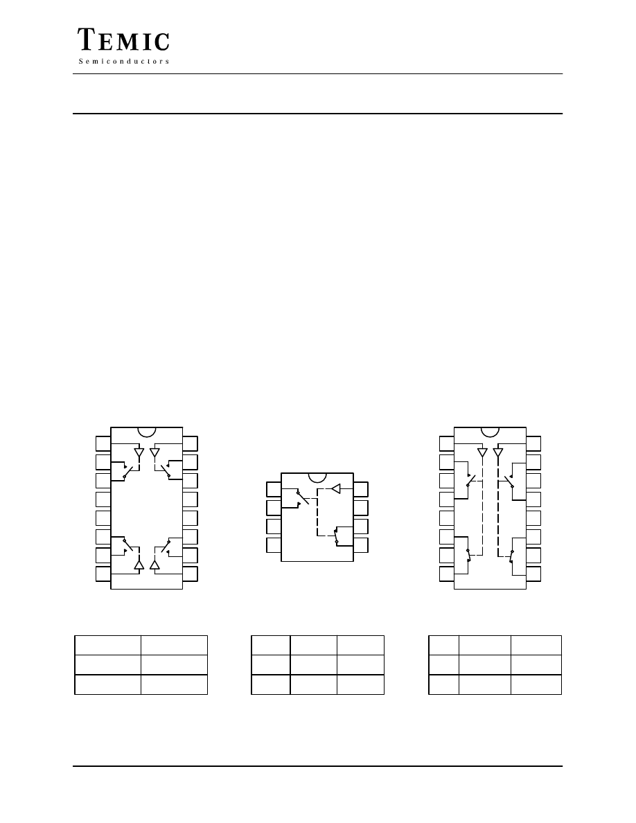
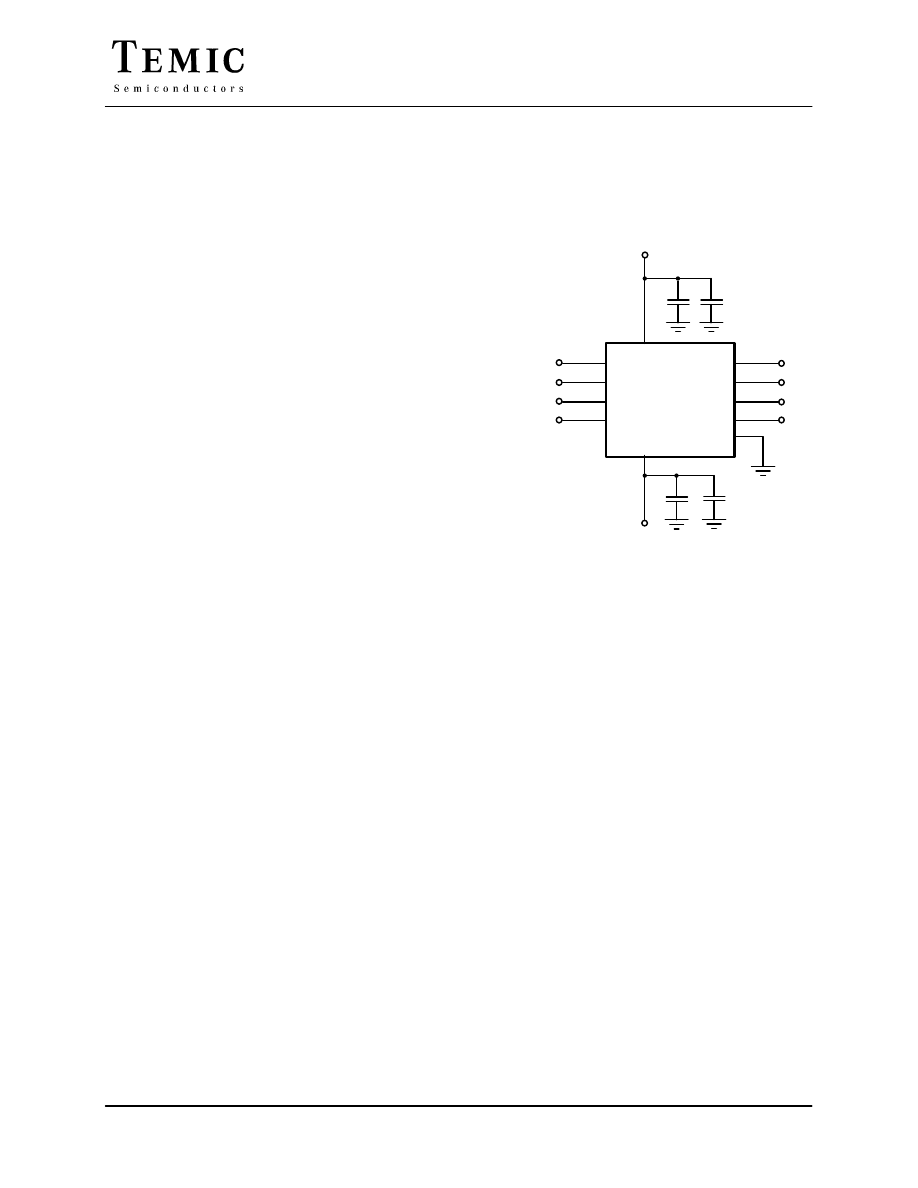
Functional Block Diagram and Pin Configuration
SW
1
, SW
2
OFF
ON
DG641
IN
1
IN
2
D
1
D
2
S
1
S
2
V–
V+
GND
GND
S
4
S
3
D
4
D
3
IN
4
IN
3
Dual-In-Line and SOIC
Truth Table—DG641
Logic “0”
0.8 V
Logic “1”
2.4 V
Logic
Switch
0
1
OFF
ON
Truth Table—DG642
Logic “0”
0.8 V
Logic “1”
2.4 V
Logic
SW
2
0
1
ON
OFF
Truth Table—DG643
Logic “0”
0.8 V
Logic “1”
2.4 V
Logic
0
1
DG642
D
2
GND
Dual-In-Line and SOIC
S
2
S
1
IN
D
1
V+
V–
IN
1
IN
2
D
1
D
2
GND
GND
S
1
S
2
V–
V+
S
4
S
3
GND
GND
D
4
D
3
Dual-In-Line and SOIC
DG643
SW
1
OFF
ON
SW
3
, SW
4
ON
OFF
Updates to this data sheet may be obtained via facsimile by calling Siliconix FaxBack, 1-408-970-5600. Please request FaxBack document #70058.
DG641/642/643
2
Siliconix
S-52880—Rev. D, 28-Apr-97
Ordering Information
Temp Range
Package
Part Number
DG641
–40 to 85
_C
16-Pin Plastic DIP
DG641DJ
–40 to 85
_C
16-Pin Narrow SOIC
DG641DY
DG642
–40 to 85
_C
8-Pin Plastic DIP
DG642DJ
–40 to 85
_C
8-Pin Narrow SOIC
DG642DY
DG643
–40 to 85
_C
16-Pin Plastic DIP
DG643DJ
–40 to 85
_C
16-Pin Narrow SOIC
DG643DY
Absolute Maximum Ratings
V+ to V–
–0.3 V to 21 V
. . . . . . . . . . . . . . . . . . . . . . . . . . . . . . . . . . . . .
V+ to GND
–0.3 V to 21 V
. . . . . . . . . . . . . . . . . . . . . . . . . . . . . . . . . . . .
V– to GND
–19 V to +0.3 V
. . . . . . . . . . . . . . . . . . . . . . . . . . . . . . . . . . .
Digital Inputs
(V–) –0.3 V to (V+) +0.3 V
. . . . . . . . . . . . . . . . . . . . . . . .
or 20 mA, whichever occurs first
V
S
, V
D
(V–) –0.3 V to (V–) +14 V
. . . . . . . . . . . . . . . . . . . . . . . . . . . . .
or 20 mA, whichever occurs first
Continuous Current (Any Terminal Except S or D)
20 mA
. . . . . . . . . . .
Continuous Current S or D: DG641/643
75 mA
. . . . . . . . . . . . . . . . . . .
DG642
100 mA
. . . . . . . . . . . . . . . . . . . . . .
Current, S or D (Pulsed 1 ms, 10% duty cycle max)
DG641/643
200 mA
. . . . . . . . . . . . . . . . . .
DG642
300 mA
. . . . . . . . . . . . . . . . . . . . . .
Storage Temperature
–65 to 125
_C
. . . . . . . . . . . . . . . . . . . . . . . . . . . . .
Power Dissipation (Package)
b
8-Pin Plastic DIP and Narrow SOIC
c
300 mW
. . . . . . . . . . . . . . . . . . . . .
16-Pin Plastic DIP
d
470 mW
. . . . . . . . . . . . . . . . . . . . . . . . . . . . . . . . . .
16-Pin Narrow SOIC
e
600 mW
. . . . . . . . . . . . . . . . . . . . . . . . . . . . . . . .
Notes:
a.
Signals on S
X
, D
X
, or IN
X
exceeding V+ or V– will be clamped by
internal diodes. Limit forward diode current to maximum current
ratings.
b.
All leads welded or soldered to PC Board.
c.
Derate 7.6 mW/
_C above 75_C
d.
Derate 6 mW/
_C above 75_C
e.
Derate 10 mW/
_C above 75_C
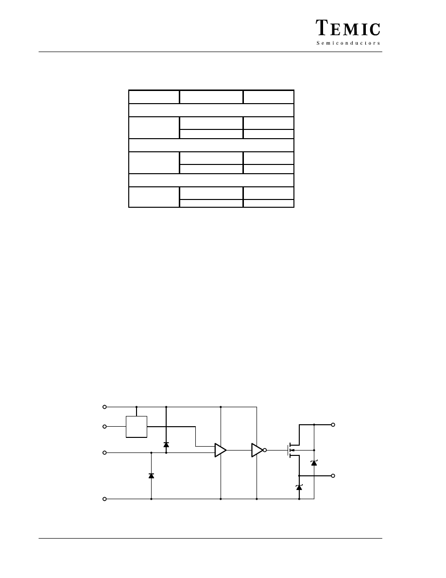
Schematic Diagram (Typical Channel)
Figure 1.
D
S
V+
IN
V–
5 V
Reg
GND
DG641/642/643
Siliconix
S-52880—Rev. D, 28-Apr-97
3
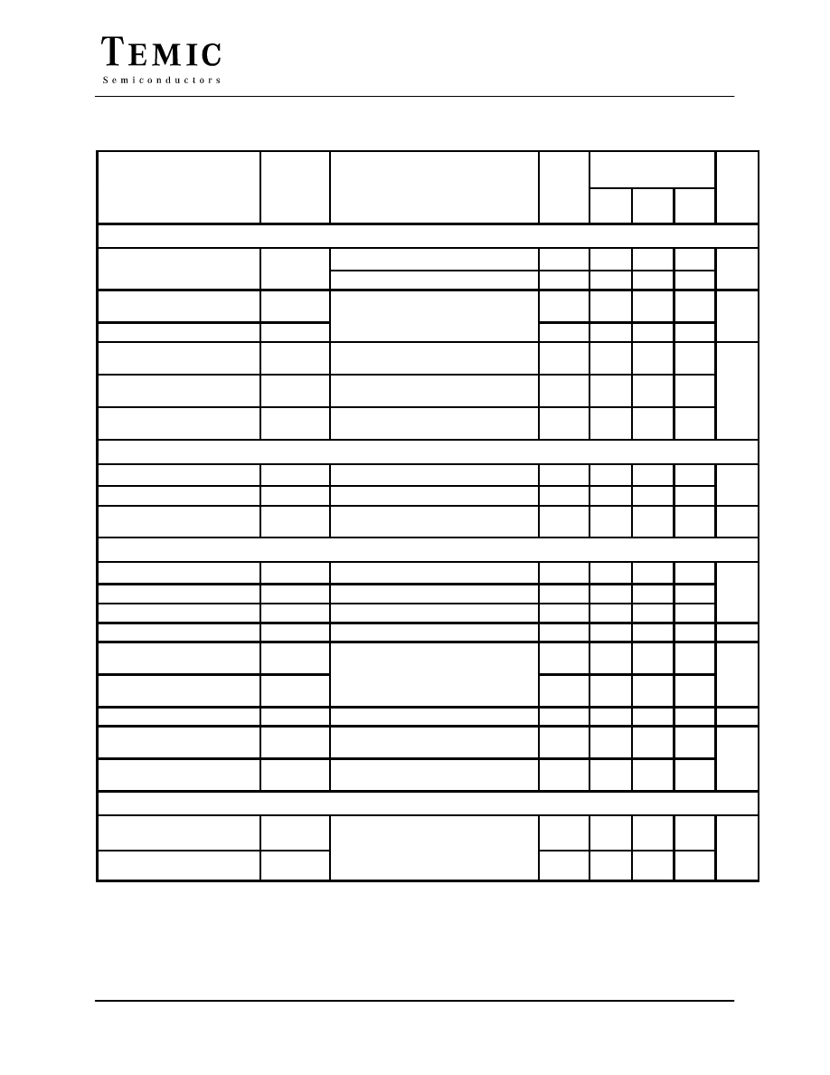
Specifications for DG641 and DG643
Test Conditions
Unless Otherwise Specified
Limits
–40 to 85
_C
Parameter
Symbol
V+ = 15 V, V– = –3 V
V
INH
= 2.4 V, V
INL
= 0.8 V
e
Temp
a
Min
c
Typ
b
Max
c
Unit
Analog Switch
Analog Signal Range
d
V
ANALOG
V– = –5 V, V+ = 12 V
Full
–5
8
V
Analog Signal Range
d
V
ANALOG
V– = GND, V+ = 12 V
Full
0
8
V
Drain-Source On-Resistance
r
DS(on)
I
S
= –10 mA, V
D
= 0 V
Room
Full
8
15
20
W
r
DS(on)
Match
Dr
DS(on)
S
,
D
Room
1
2
Source Off Leakage Current
I
S(off)
V
S
= 0 V, V
D
= 10 V
Room
Full
–10
–100
–0.02
10
100
Drain Off Leakage Current
I
D(off)
V
S
= 10 V, V
D
= 0V
Room
Full
–10
–100
–0.02
10
100
nA
Channel On Leakage Current
I
D(on)
V
S
= V
D
= 0 V
Room
Full
–10
–100
–0.1
10
100
Digital Control
Input Voltage High
V
INH
Full
2.4
V
Input Voltage Low
V
INL
Full
0.8
V
Input Current
I
IN
V
IN
= GND or V+
Room
Full
–1
–20
0.05
1
20
mA
Dynamic Characteristics
On State Input Capacitance
d
C
S(on)
V
S
= V
D
= 0 V
Room
10
20
Off State Input Capacitance
d
C
S(off)
V
S
= 0 V
Room
4
12
pF
Off State Output Capacitance
d
C
D(off)
V
D
= 0 V
Room
4
12
Bandwidth
BW
R
L
= 50
W, See Figure 6
Room
500
MHz
Turn On Time
t
ON
R
L
= 1 k
W C
L
= 35 pF See Figure 2
Room
Full
50
70
140
ns
Turn Off Time
t
OFF
R
L
= 1 k
W, C
L
= 35 pF, See Figure 2
Room
Full
28
50
85
ns
Charge Injection
Q
C
L
= 1000 pF, V
D
= 0 V, See Figure 3
Room
–19
pC
Off Isolation
OIRR
R
IN
= 75
W, R
L
= 75
W, f = 5 MHz
See Figure 4
Room
–60
dB
All Hostile Crosstalk
X
TALK(AH)
R
IN
= 10
W, R
L
= 75
W, f = 5 MHz
See Figure 5
Room
–87
dB
Power Supplies
Positive Supply Current
I+
V
IN
= 0 V or V
IN
= 5 V
Room
Full
3.5
6
9
mA
Negative Supply Current
I–
V
IN
= 0 V or V
IN
= 5 V
Room
Full
–6
–9
–3
mA
Notes:
a.
Room = 25
_C, Full = as determined by the operating temperature suffix.
b.
Typical values are for DESIGN AID ONLY, not guaranteed nor subject to production testing.
c.
The algebraic convention whereby the most negative value is a minimum and the most positive a maximum, is used in this data sheet.
d.
Guaranteed by design, not subject to production test.
e.
V
IN
= input voltage to perform proper function.
DG641/642/643
4
Siliconix
S-52880—Rev. D, 28-Apr-97
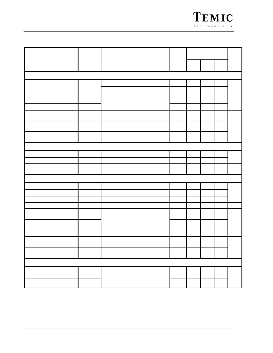
Specifications for DG642
Test Conditions
Unless Otherwise Specified
Limits
–40 to 85
_C
Parameter
Symbol
V+ = 15 V, V– = –3 V
V
INH
= 2.4 V, V
INL
= 0.8 V
e
Temp
a
Min
c
Typ
b
Max
c
Unit
Analog Switch
Analog Signal Range
d
V
ANALOG
V– = –5 V, V+ = 12 V
Full
–5
8
V
Analog Signal Range
d
V
ANALOG
V– = GND, V+ = 12 V
Full
0
8
V
Drain-Source On-Resistance
r
DS(on)
I
S
= –10 mA, V
D
= 0 V
Room
Full
5
8
9
W
r
DS(on)
Match
Dr
DS(on)
S
,
D
Room
0.5
1
Source Off Leakage Current
I
S(off)
V
S
= 0 V, V
D
= 10 V
Room
Full
–10
–200
–0.04
10
200
Drain Off Leakage Current
I
D(off)
V
S
= 10 V, V
D
= 0V
Room
Full
–10
–200
–0.04
10
200
nA
Channel On Leakage Current
I
D(on)
V
S
= V
D
= 0 V
Room
Full
–10
–200
–0.2
10
200
Digital Control
Input Voltage High
V
INH
Full
2.4
V
Input Voltage Low
V
INL
Full
0.8
V
Input Current
I
IN
V
IN
= GND or V+
Room
Full
–1
–20
0.05
1
20
mA
Dynamic Characteristics
On State Input Capacitance
d
C
S(on)
V
S
= V
D
= 0 V
Room
19
40
Off State Input Capacitance
d
C
S(off)
V
S
= 0 V
Room
8
20
pF
Off State Output Capacitance
d
C
D(off)
V
D
= 0 V
Room
8
20
Bandwidth
BW
R
L
= 50
W, See Figure 6
Room
500
MHz
Turn On Time
t
ON
R
L
= 1 k
W C
L
= 35 pF See Figure 2
Room
Full
60
100
160
ns
Turn Off Time
t
OFF
R
L
= 1 k
W, C
L
= 35 pF, See Figure 2
Room
Full
40
60
100
ns
Charge Injection
Q
C
L
= 1000 pF, V
D
= 0 V, See Figure 3
Room
–40
pC
Off Isolation
R
IN
= 75
W, R
L
= 75
W, f = 5 MHz
See Figure 4
Room
–63
dB
All Hostile Crosstalk
X
TALK(AH)
R
IN
= 10
W, R
L
= 75
W, f = 5 MHz
See Figure 5
Room
–85
dB
Power Supplies
Positive Supply Current
I+
V
IN
= 0 V or V
IN
= 5 V
Room
Full
3.5
6
9
mA
Negative Supply Current
I–
V
IN
= 0 V or V
IN
= 5 V
Room
Full
–6
–9
–3
mA
Notes:
a.
Room = 25
_C, Full = as determined by the operating temperature suffix.
b.
Typical values are for DESIGN AID ONLY, not guaranteed nor subject to production testing.
c.
The algebraic convention whereby the most negative value is a minimum and the most positive a maximum, is used in this data sheet.
d.
Guaranteed by design, not subject to production test.
e.
V
IN
= input voltage to perform proper function.
DG641/642/643
Siliconix
S-52880—Rev. D, 28-Apr-97
5
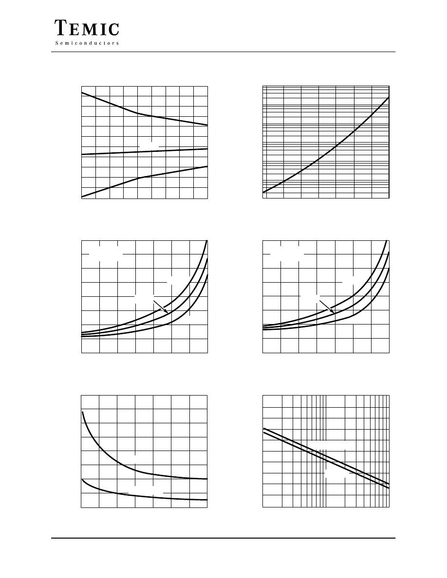
Typical Characteristics
6
5
4
3
2
1
0
–1
–2
–3
–4
–5
–55
–35 –15
5
25
45
65
85 105
125
I +
I –
Supply Current vs. Temperature
I
GND
Temperature (
_C)
Current (mA)
–55
0
125
100 nA
10 nA
1 nA
100 pA
10 pA
1 pA
Leakages vs. Temperature
Temperature (
_C)
I
D(of
f)
,I
S(of
f)
0.1 pA
–25
25
50
75
100
20
15
10
5
0
–3
–1
1
3
5
7
9
11
V+ = 15 V
V– = –3 V
DG642
r
DS(on)
vs. Drain Voltage
V
D
– Drain Voltage (V)
125
_C
25
_C
–55
_C
1
10
100
–110
–100
–90
–80
–70
–60
–50
–40
–30
–20
–10
OIRR (dB)
f – Frequency (MHz)
DG641/643
DG642
Off Isolation
22
20
18
16
14
12
10
8
6
12
10
8
6
4
2
0
C (pF)
(V
D
) – (V–)
DG642
DG641/643
On Capacitance
40
30
20
10
0
–3
–1
1
3
5
7
9
11
V+ = 15 V
V– = –3 V
125
_C
25
_C
–55
_C
DG641/643
r
DS(on)
vs. Drain Voltage
r
DS(on)
– Drain-Source On-Resistance (
V
D
– Drain Voltage (V)
r
DS(on)
– Drain-Source On-Resistance (
)
)
DG641/642/643
6
Siliconix
S-52880—Rev. D, 28-Apr-97
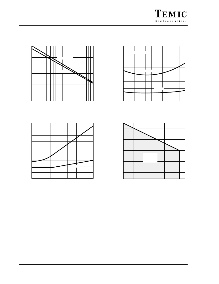
Typical Characteristics
–55
0
125
–25
25
50
75
100
10
12
14
16
18
20
–4
–3
–2
–1
0
Operating
Voltage
Area
V+ – Positive Supply
V
oltage (V)
–6
–5
1
10
100
110
100
90
80
70
60
50
40
30
20
10
(dB)
X
T
ALK
All Hostile Crosstalk
f – Frequency (MHz)
DG642
DG641/643
0
–10
–20
–30
–40
8
4
2
0
–2
–3
6
–1
1
3
5
7
Q (pC)
Charge Injection vs. V
D
DG642
DG641/643
C
L
= 1000 pF
90
70
60
50
40
30
20
10
0
80
Switching Times vs. Temperature
t (ns)
Temperature (
_C)
t
ON
t
OFF
V
D
– Drain Voltage (V)
V– – Negative Supply (V)
Operating Supply Voltage Range
DG641/642/643
Siliconix
S-52880—Rev. D, 28-Apr-97
7
Test Circuits
Figure 2.
Switching Time
Figure 3.
Charge Injection
3 V
0
90%
90%
50%
t
OFF
t
ON
t
r
<20 ns
t
f
<20 ns
Logic
Input
Switch
Output
ON
ON
OFF
V
O
DV
O
IN
X
DV
O
= measured voltage error due to charge injection
The charge injection in coulombs is Q = C
L
x
DV
O
Figure 4.
Off Isolation
3 V
V–
V+
IN
S
C
L
35 pF
D
3 V
R
L
1 k
W
V
O
–3 V
GND
+15 V
C
L
1000 pF
3 V
V
g
V
O
D
V+
R
g
S
IN
V–
–3 V
GND
+15 V
S
IN
R
L
D
R
g
= 50
W
V
S
V
O
0V, 2.4 V
Off Isolation = 20 log
V
S
V
O
V+
–3 V
GND
V–
C
C
+15 V
DG641/642/643
8
Siliconix
S-52880—Rev. D, 28-Apr-97
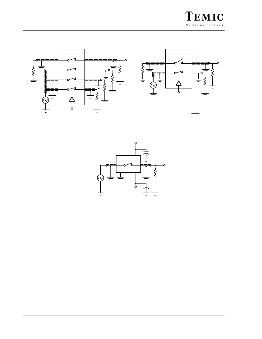
Test Circuits
Figure 5.
All Hostile Crosstalk – X
TALK(AH)
Signal
Generator
75
W
S
1
S
2
“0”
V
OUT
R
L
75
W
R
L
R
L
R
L
R
IN
10
W
S
1
S
2
S
3
S
4
“1”
D
1
D
2
D
3
D
4
Signal
Generator
75
W
R
IN
10
W
V
(a)
DG641
(b)
DG642
R
L
D
1
D
2
V
+15 V
–3 V
V+
V–
Signal
Generator
50
W
V
OUT
R
L
50
W
S
D
Figure 6.
Bandwidth
V
OUT
R
L
75
W
X
TALK(AH)
20 log
10
V
OUT
V
Applications
Device Description
The DG641/642/643 switches offer true bidirectional
switching of high frequency analog or digital signals with
minimum signal crosstalk, low insertion loss, and
negligible non-linearity distortion and group delay.
Built on the Siliconix D/CMOS process, these switches
provide excellent off-isolation with a bandwidth of around
500 MHz. The silicon-gate D/CMOS processing also yields
fast switching speeds.
An on-chip regulator circuit maintains TTL input
compatibility over the whole operating supply voltage
range shown, easing control logic interfacing.
Circuit layout is facilitated by the interchangeability of
source and drain terminals.
Frequency Response
A single switch on-channel exhibits both resistance
[r
DS(on)
] and capacitance [C
S(on)
]. This RC combination has
an attenuation effect on the analog signal – which is
frequency dependent (like an RC low-pass filter). The
–3
dB bandwidth of the DG641/642/643 is typically
500 MHz (into 50
W).
DG641/642/643
Siliconix
S-52880—Rev. D, 28-Apr-97
9
Applications (Cont’d)
Power Supplies
Power supply flexibility is a useful feature of the
DG641/642/643 series. It can be operated from a single
positive supply (V+) if required (V– connected to ground).
Note that the analog signal must not exceed V– by more
than –0.3 V to prevent forward biasing the substrate p-n
junction. The use of a V– supply has a number of
advantages:
1.
It allows flexibility in analog signal handling, i.e., with
V– = –5 V and V+ = 12 V; up to
5-V ac signals can be
controlled.
2.
The value of on capacitance [C
S(on)
] may be reduced. A
property known as ‘the body-effect’ on the DMOS
switch devices causes various parametric effects to
occur. One of these effects is the reduction in C
S(on)
for
an increasing V body-source. Note however that to
increase V– normally requires V+ to be reduced (since
V+ to V– = 21 V max.). A reduction in V+ causes an
increase in r
DS(on)
, hence a compromise has to be
achieved. It is also useful to note that tests indicate that
optimum video linearity performance (e.g., differential
phase and gain) occurs when V– is around –3 V.
3.
V– eliminates the need to bias the analog signal using
potential dividers and large coupling capacitors.
Decoupling
It is an established rf design practice to incorporate
sufficient bypass capacitors in the circuit to decouple the
power supplies to all active devices in the circuit. The
dynamic performance of the DG641/642/643 series is
adversely affected by poor decoupling of power supply
pins. Also, of even more significance, since the substrate of
the device is connected to the negative supply, adequate
decoupling of this pin is essential. Suitable decoupling
capacitors are 1- to 10-
mF tantalum bead, plus 10- to 100-nF
ceramic or polyester.
Rules:
1.
Decoupling capacitors should be incorporated on all
power supply pins (V+, V–). (See Figure 7).
2.
They should be mounted as close as possible to the
device pins.
3.
Capacitors should be of a suitable type with good high
frequency characteristics – tantalum bead and/or
ceramic disc types are adequate.
+
+
–3 V
GNDs
+15 V
DG64X
V+
V–
S
1
S
2
S
3
S
4
D
1
D
2
D
3
D
4
C
1
C
2
C
1
C
2
C
1
= 10
mF Tantalum
C
2
= 0.1
mF Ceramic
Figure 7.
Supply Decoupling
Board Layout
PCB layout rules for good high frequency performance
must also be observed to achieve the performance boasted
by these analog switches. Some tips for minimizing stray
effects are:
1.
Use extensive ground planes on double sided PCB,
separating adjacent signal paths. Multilayer PCB is
even better.
2.
Keep signal paths as short as practically possible, with
all channel paths of near equal length.
3.
Careful arrangement of ground connections is also very
important. Star connected system grounds eliminate
signal current, flowing through ground path parasitic
resistance, from coupling between channels.
Figure 8 shows a 4-channel video multiplexer using a DG641.
In Figure 9, two coax cables terminated on 75
W bring two
video signals to the DG642 switch. The two drains tied
together lower the on-state capacitance. An Si582 video
amplifier drives a double terminated 75-
W cable. The
double terminated coax cable eliminates line reflections.
DG641/642/643
10
Siliconix
S-52880—Rev. D, 28-Apr-97
Applications (Cont’d)
+
–
+15 V
V+
V–
–3 V
TTL Channel Select
A = 2
75
W
250
W
Si582
CH
1
CH
2
CH
3
CH
4
DG641
DIS
75
W
75
W
75
W
75
W
250
W
+
–
+15 V
V+
V–
–3 V
TTL Channel Select
A = 2
Si582
CH
1
CH
2
DG642
DIS
250
W
75
W
250
W
75
W
R
L
75
W
75
W
V
OUT
S
1
S
2
D
1
D
2
fc
1
2
p
R
3
C
x
fc SELECT
IN
2
S
2
S
3
D
2
D
3
C
1
C
2
R
3
1
/
2
DG643
R
1
R
2
V
OUT
S
1
S
4
D
1
D
4
IN
1
CH
1
CH
2
CH SELECT
LF401
–
+
Figure 8.
4 by 1 Video Multiplexing Using the DG641
Figure 9.
2-Channel Video Selector Using the DG642
Figure 10.
Active Low Pass Filter with Selectable Inputs and Break Frequencies
1
/
2
DG643
Wyszukiwarka
Podobne podstrony:
46 643 656 Vacuum HT of Hot Work Steel
644 odp do 643
Angielski Present Simple id 643 Nieznany (2)
643
642 643
643
643
Dz.U. 2010 nr 100 poz. 643
643
643
643
46 643 656 Vacuum HT of Hot Work Steel
000 643
643
NACA 643 The Aerodynamic Characteristics of Four Full Scale Propellers
643 Zestawienie zmian w kapitale (funduszu) własnym
więcej podobnych podstron