Document Number: 35044
For technical questions contact: frequency@vishay.com
www.vishay.com
Revision: 05-Mar-07
27
Half Size Clock Oscillators Enable/Disable
XO-523
Vishay Dale
The XO-523 series oscillator is half size, has Tri-state
enable/disable controlled function, and is with a 3.3 V power
supply voltage. The metal package with pin#4 case ground
acts as shielding to minimize EMI radiation.
FEATURES
•
Tri-state enable/disable
• 8 pin half size
• Industry standard
• Wide frequency range
• Low cost
• Resistance weld package
• 3.3 V
• Lead (Pb)-free terminations and RoHS compliant
RoHS
COMPLIANT
* Include: 25 ºC tolerance, operating temperature range, input voltage change, aging, load change, shock and vibration.
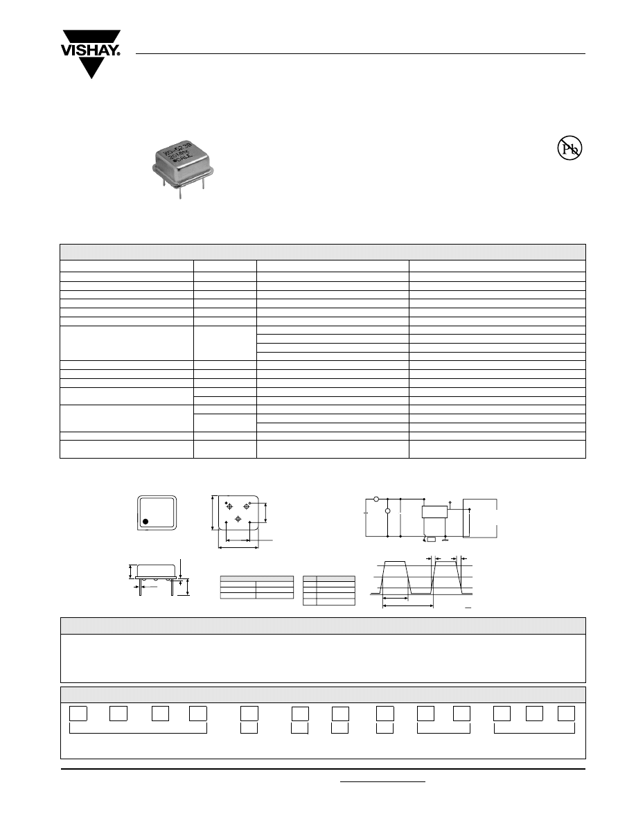
DIMENSIONS in inches [millimeters]
STANDARD ELECTRICAL SPECIFICATIONS
PARAMETER
SYMBOL
CONDITION
XO-523
Frequency Range
F
O
1 MHz ~ 100.00 MHz
Frequency Stability*
All Condition*
± 25 ppm, ± 50 ppm, ± 100 ppm
Operating Temperature Range
T
OPR
0 °C ~ 70 °C (- 40 °C ~ + 85 °C option)
Storage Temperature Range
T
STG
- 55 °C ~ + 125 °C
Power Supply Voltage
V
DD
3.3 V ± 10 %
Aging (First Year)
25 ºC ± 3 ºC
± 5 ppm
Supply Current
I
DD
1 MHz to 23.999 MHz
15 mA Max
24.000 MHz to 49.999 MHz
20 mA Max
50.000 MHz to 69.999 MHz
30 mA Max
70.000 MHz to 100.000 MHz
45 mA Max
Output Symmetry
Sym
At 1/2 V
DD
40/60 % (45/55 % Option)
Rise Time
T
r
20 % V
DD
~ 80 % V
DD
8 ns Max
Fall Time
T
f
80 % V
DD
~ 20 % V
DD
8 ns Max
Output Voltage
V
OH
90 % V
DD
Min
V
OL
10 % V
DD
Max
Output Load
TTL Load
1 ~ 5 TTL
HCMOS Load
~ 50 M : 30 pF
~ 125 M : 15 pF
Start-up Time
Ts
10 ms Max
Pin 1, tri-state function
Pin 1 = H or open... Output active at pin 5
Pin 1 = L... high impedance at pin 5
MARKING
AREA
HCMOS TEST CIRCUIT
0.220
[5.6] Max
[0.45 ± 0.1]
[0.8 ± 0.1]
0.268
[6.80] Max
HCMOS OUTPUT WAVEFORM
0.031 ± 0.003
0.018 ± 0.003
V
OH
V
OL
T
r
T
f
90 % V
DD
50 % V
DD
10 % V
DD
GND
T1
T0 = 1/Fo
SYMMETRY = x 100 %
T1
T0
+ 5.0 V
Test Point
CL**
0.01 µF
CMOS Load
**Includes Stray and Probe Capacitance
INH
+ 3.3 V
Enable/Disable function
ENABLE/DISABLE FUNCTION
INPUT (PIN 1)
OPEN
V
IH
≥ 2.2 V
DC
OUTPUT (PIN 5)
ENABLE
ENABLE
PIN
#1
#4
#5
#8
CONNECTION
N.C
GND
OUTPUT
V
DD
#1
#4
#5
#8
0.508
[12.9] Max
0.300 ± 0.005
[7.62 ± 0.13]
0.580 [12.9] Max
0.300 ± 0.005
[7.62 ± 0.13]
A
V
#8
#1
#5
#4
CL = 15 pF or 50 pF
(see individual
spec. sheet)
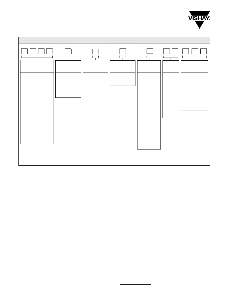
ORDERING INFORMATION
XO-523
MODEL
B
FREQUENCY
STABILITY
AA = 0.0025 % (25 ppm)
A = 0.005 % (50 ppm)
R
OTR
Blank = 0 °C to + 70 °C
R = - 40 °C to + 85 °C
E
ENABLE/DISABLE
Blank = Pin 1 open
E = Disable to Tristate
40 M
FREQUENCY/MHz
e2
JEDEC
LEAD (Pb)-FREE
STANDARD
GLOBAL PART NUMBER
MODEL
FREQUENCY
STABILITY
OTR
ENABLE/
DISABLE
PACKAGE
CODE
OPTIONS
FREQUENCY
X
O
3
2
C
T
E
L
N
A
4
0
M
www.vishay.com
For technical questions contact: frequency@vishay.com
Document Number: 35044
28
Revision: 05-Mar-07
XO-523
Vishay Dale
Half Size Clock Oscillators Enable/Disable
GLOBAL PART NUMBERING
X
O
5
2
C
T
E
L
N
A
4
0
M
MODEL NUMBER
FREQUENCY
STABILITY
OPERATING
TEMPERATURE
(OTR)
ENABLE/
DISABLE
PACKAGE
CODE
OPTIONS
FREQUENCY
XO53 = XO-53
XO54 = XO-54
XO34 = XO-543
XO52 = XO-52
XO32 = XO-523
XO56 = XO-56
XOVC = XOVC-23
XO5M = XOSM-52
XO63 = XOSM-533
XO62 = XOSM-532
XO61 = XOSM-531
XO57 = XOSM-57
XO37 = XOSM-573
XO27 = XOSM-572
XO17 = XOSM-571
XO55 = XOSM-55
XO35 = XOSM-553
C = 0.01 %
(100 ppm)
D = 0.005 %
(50 ppm)
E = 0.0025 %
(25 ppm)
T = 0 °C to + 70 °C
R = - 40 °C to + 85 °C
F = Pin 1 Open
E = Disable to
Tristate
TAPE AND
REEL
H = RF7
BULK
A = B04
(XO63, XO62,
XO61)
C = D06
(XO57, XO37,
XO27, XO17)
D = D07
(XO53, XO54,
XO34, XO56,
XOVC, XO55,
XO35)
L = D08
(XO52, XO32,
XO5M)
NA = No
Additional
Options
60 = 45/55
Symmetry
Contact
factory for
all other
options
4M = 4 MHz
40M = 40 MHz
100M = 100 MHz
12M288 = 12.288 MHz
M is used as
decimal place
holder in frequency
Example: XO52CTELNA40M

Legal Disclaimer Notice
Vishay
Document Number: 91000
www.vishay.com
Revision: 08-Apr-05
1
Notice
Specifications of the products displayed herein are subject to change without notice. Vishay Intertechnology, Inc.,
or anyone on its behalf, assumes no responsibility or liability for any errors or inaccuracies.
Information contained herein is intended to provide a product description only. No license, express or implied, by
estoppel or otherwise, to any intellectual property rights is granted by this document. Except as provided in Vishay's
terms and conditions of sale for such products, Vishay assumes no liability whatsoever, and disclaims any express
or implied warranty, relating to sale and/or use of Vishay products including liability or warranties relating to fitness
for a particular purpose, merchantability, or infringement of any patent, copyright, or other intellectual property right.
The products shown herein are not designed for use in medical, life-saving, or life-sustaining applications.
Customers using or selling these products for use in such applications do so at their own risk and agree to fully
indemnify Vishay for any damages resulting from such improper use or sale.
Document Outline
Wyszukiwarka
Podobne podstrony:
XO 52 (Vishay)
XO 543 (Vishay)
XO 54 (Vishay)
04 Wyklad4 predykcja sieci neuronoweid 523 (2)
523
oświadczenie o zagubieniu legitymacjiid 523
Ćw 523, MIBM WIP PW, fizyka 2, laborki fiza(2), 37-Dyfrakcja elektronów i światła na sieci krystalic
523
523, PlanTestowMoj, Punkty funkcyjne
523, BYTMaciejJedlinski, Struktura projektu
Hahn i Hahn s 491 523
PN IEC 60364 5 523 2001
BYV27 50 BYV27 200 (Vishay)
BF970 Vishay elenota pl
FRFU 61 t2 523 id 181029 Nieznany
kpk, ART 523 KPK, WK 6/06 - postanowienie z dnia 13 lipca 2006 r
523
523
więcej podobnych podstron