Loop Areas
Close 'Em Tight!
Douglas Brooks, President
UltraCAD Design, Inc.
www.ultracad.com
One of the absolutely fundamental truths in electronics
is that current flows in a closed loop. Current is the flow of
electrons, and if it were not true that current flows in a
closed loop, then electrons would start collecting in some
sort of pool somewhere along a wire or trace. Intuitively, we
know this doesn't happen.
If current does flow in a closed loop, then it is also ab-
solutely, fundamentally true that every signal has an equal
and opposite return signal associated with it.
When we design a PC board, we carefully design the
path that the signal takes. But we often don't consider the
path of the return signal. We simply take for granted that
the return signal will sort of take care of itself. It turns out
that in high speed designs it's pretty important for the de-
signer to know where the return path is for each (and every)
signal. It does exist. The only question is "Where is it?"
If current flows in a closed loop, then we can visualize
the area defined by that loop. Take, for example, a twisted
pair of wires with the signal on one wire and the return on
the other. Since the wires are twisted closely together, the
loop area is pretty small. A coax cable with the signal on the
center conductor and the return on the shield also has a very
small loop area. But, if we had, for example, a ten inch long
trace with a return trace one inch away, we would have a
loop area of 10 in
2
, much larger than in the other two cases.
Loop Area:
"So what?" you ask. Well there are several possible
sources of EMI on a board, but a significant one is the loop
area around which a very high speed signal propagates. EMI
is related to loop area. In the case of twisted pairs and coax
cables, loop areas are small and these configurations per-
form well in EMI environments. But in the case of the sig-
nal and return traces being separated, the loop area might
become significant, and such a configuration might radiate
badly.
That's why it is important for a designer to know where
the return signal path is, and to make sure that the loop area
defined by the signal and its return is as small as possible.
We almost always use power and ground planes in high
speed designs. There are a variety of reasons for doing so
(see "Brookspeak: Ground Plane 101", October, 1997, p.34).
One of them is that if a signal trace exists above a (power or
ground) plane, the return signal will be on the plane directly
below the trace. The reason for this is complicated, but
let me try to simplify it in a couple of sentences.
Assume there are two traces, side by side, one with
a signal and the other with its return. A fast rising sig-
nal will create an expanding magnetic field that will
induce an opposite signal on the return trace. This sig-
nal actually reinforces the return signal. The return sig-
nal also creates an expanding magnetic field that in-
duces a current in the signal trace that correspondingly
reinforces the signal current. This coupling
(reinforcement) increases as the two traces move closer
together. The stronger the mutual reinforcement, the
lower the overall impedance to the signal flow. There-
fore, the signal and its return will naturally want to be
as close as possible. If we constrain the signals to wires
or traces, then they will be where we put them. But if
the return signal is on a plane, it will by nature want to
be where the overall impedance is the lowest possible,
which will be as close to the trace as possible--i.e. di-
rectly underneath it.
A signal trace whose return is on a plane directly
under it has a small loop area.
Well designed boards, those with planes where re-
turn signals can travel directly under their correspond-
ing signal traces, perform well in EMI critical environ-
ments. We get into trouble when we cause the signal
return to move away from under the signal trace, creat-
ing a loop. But, we usually don't do this on purpose!
The rest of this article will illustrate some common de-
sign problems that cause loop areas to increase.
Excessive pin clearance:
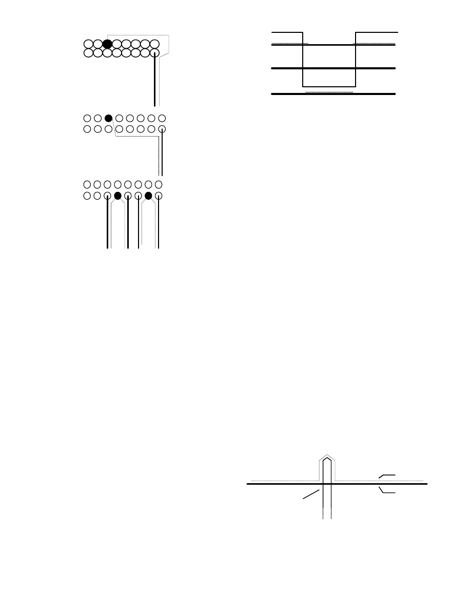
Figure 1 (a) illustrates a trace leading to a pin on a
connector. Clearance pads are so large that there is no
copper for the return trace to find its way through to a
ground pin. Thus the return signal must circle around
the connector to the ground pin, causing what might be
a significant loop resulting in unacceptable EMI radia-
tion. A better strategy is to limit the clearance so there
are copper paths between the pins for the return signals
to follow, as shown in (b). But the best strategy is (c),
making appropriate pin assignments so that there is a
ground (signal return) pin near every signal pin.
This article appeared in Printed Circuit Design Magazine, January, 1999
1999 Miller Freeman, Inc.
1999 UltraCAD Design, Inc.

Now, what if the signal trace is referenced to (is directly
adjacent to) a power plane instead of a ground plane? The
difference between a power plane and a ground plane is pri-
marily a DC distinction. AC signals can travel with ease on
any plane. So if a signal is referenced to a power plane, how
does the return signal get from the power plane to the
ground pin at the connector? The practical answer is that
there are usually enough bypass capacitors (between power
and ground) nearby to provide a suitable path for the return
signal. Some experts, however, actually recommend the
placement of one or more bypass caps near a connector
specifically to provide for signal return paths.
Vias:
Figure 2 illustrates the case of a signal moving from
one signal layer to another through a via. It should be clear
that the designer needs to be sure that the characteristic
impedance of the trace (Zo) is the same along all segments,
otherwise reflections will be caused at the vias. But what
about the return signal? If it has to find a circuitous loop
between the various planes that are adjacent to the trace,
then unacceptable loop areas (and EMI radiation) might re-
sult.
I have talked with several experts about this, and we are
not aware of any definitive studies about this particular ef-
fect. Many experts feel that while it is acceptable practice to
move a signal through a via to opposite sides of the same
plane, great care should be taken when moving a signal to a
layer where it will reference to a different plane. Some ex-
perts, however, have no problem with this practice, and still
others recommend placing a bypass cap near each via for the
specific purpose of providing a path for the signal return.
Slots in planes:
There are many reasons to avoid slots in planes (see an
upcoming article about this topic in a few months.) Figure 3
illustrates one of them. If a signal traces crosses a slot,
where does the return signal go? It must find its way around
the slot and a loop is inevitable. There is simply no good
purpose for a slot in a plane in high speed designs, and lots
of really good reasons not to allow them.
Crossing unrelated planes:
We often try to isolate certain types of circuits from
other ones. Separating analog circuits from digital ones is
routine. An engineer might want to set up two different digi-
tal areas if it is critical that they be isolated from each other
for noise purposes. Standard practice is to never allow a
trace to cross over an unrelated plane.
(a)
(b)
(c)
Figure 1
Excessive through hole pin clearance or poor pin as-
signment strategies can lead to excessive loop area.
Plane
Plane
Plane
Return
Signal
?
?
?
?
Figure 2
When a signal trace transitions to a different layer, it is
not clear what happens to the return signal.
Plane
Slot
Signal
Return
Figure 3
Slots in planes almost always cause loop areas to
increase.

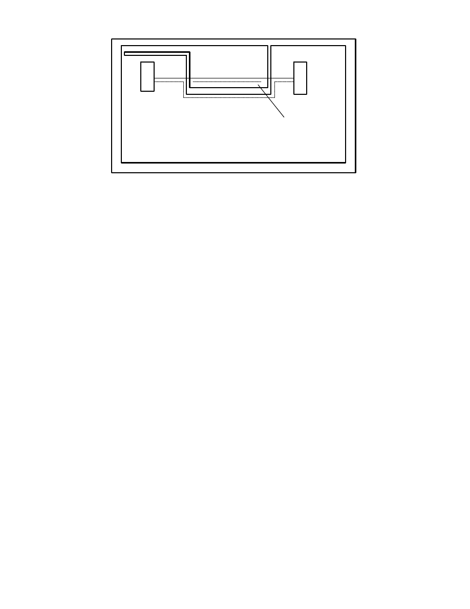
Figure 4 illustrates why. A digital signal trace crosses
over part of an analog plane. Where will the return signal be?
There are two possibilities, both of them bad! One possibility
is that the return signal will find its way onto the analog
plane. This may reduce the loop area but it will in all likeli-
hood allow noise coupling between the digital and analog
signals, defeating the whole purpose for separate circuits in
the first place. The other possibility is that the return signal
will stay on the (in this case) digital plane, resulting in a loop
that might well radiate and cause EMI problems. The solu-
tion is to never route a signal over an unrelated plane.
Analog Plane
Digital Plane
IC1
IC2
Trace
Return?
Coupled noise to
Analog Signals
Summary:
These examples illustrate that the occurrence of loop
areas can be pretty subtle. They can occur in places and at
times that we wouldn't intuitively expect. So designers are
well counseled to keep two things in mind during the de-
sign process: (1) all signals have a return path, and (2) you
really ought to know where they are!
Figure 4
If a high speed trace is routed over an unrelated plane, the result will be increased
noise, increased loop area, or both.
Wyszukiwarka
Podobne podstrony:
EM DYSTRYBUCJA
EM t 4 Ceny
EM t 6 produkcja
Close Quarers Battle Czarna Taktyka
Poker współczesny Texas Hold'em i inne odmiany pokera (2)
em
Pisownia ę ą en em om
EM cz1
WYZNACZANIE STOSUNKU em ŁADUNKU ELEKTRONU DO JEGO MASY METODĄ MAGNETRONU
2 Wyznaczanie stosunku em ładunku elektronu do jego masy metodą magnetronu
EM U A wyk 11 12
IMIR drgania EM prady zmienne i Nieznany
Deutsch als Fremdsprache Em Uebungsgrammatik
2011 EM BF zadania 03
ISO128 50 areas of sections
STOS-EM, 1 STUDIA - Informatyka Politechnika Koszalińska, Labki, fizyka1, fiza, fizyka
C 4, MIBM WIP PW, fizyka 2, laborki fiza(2), 31-Ruch elektronu w polu magnetycznym i elektrycznym. W
Mon. pól EM, Studia, 1-stopień, inżynierka, Ochrona Środowiska, Monitoring i bioindykacja środowiska
więcej podobnych podstron