T E C H N I C A L I N F O R M A T I O N
EB-TA0104, 01.01 Rev. 4.2
1
CLASS-T DIGITAL AUDIO AMPLIFIER EVALUATION BOARD USING
DIGITAL POWER PROCESSING
TM
TECHNOLOGY
EB-TA0104
January 2001 Rev. 3.3 Board
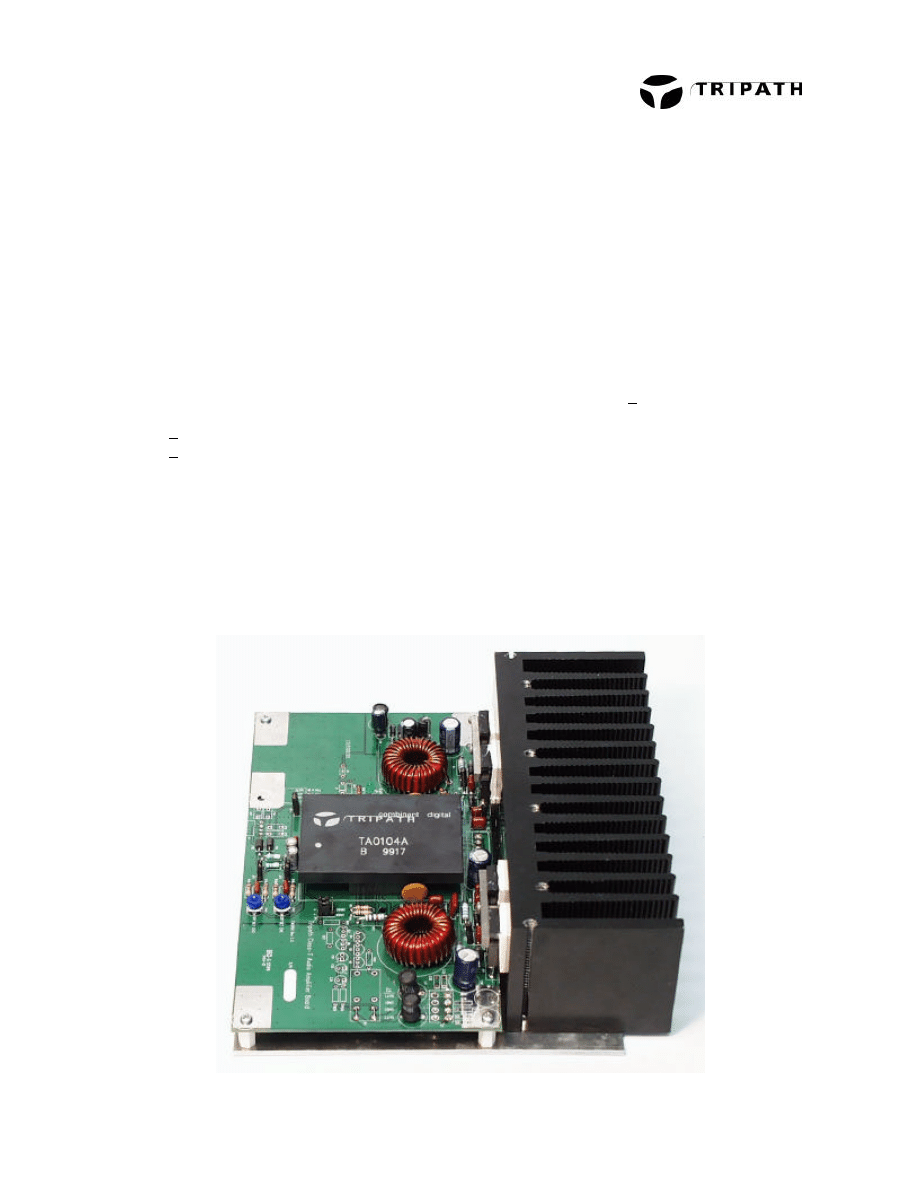
General Description
The EB-TA0104 evaluation board is based on the TA0104A digital audio power amplifier from Tripath
Technology. This board is designed to provide a simple and straightforward environment for the
evaluation of the Tripath stereo TA0104A amplifier. This board can also be used in a bridged
configuration for high power mono output.
Note: Although the maximum supply voltage limit for the TA0104A is +100V, the supply voltage
for this board is limited because of other component limitations. Do not exceed the following:
+90V for 4
Ω
Ω Single Ended Applications
+75V for 4
Ω
Ω Bridged or 2Ω
Ω Single Ended Applications
Features
Ø 2 x 400W rms @ 0.1% THD+N, 4
Ω
Ø 1000W rms bridgeable subwoofer
output, 4
Ω
@ 0.1% THD+N
Ø Four N-Channel power MOSFETs
Ø Outputs short circuit protected
Benefits
Ø Quick, easy evaluation and testing of the
TA0104A amplifier
Ø Ready to use in many applications:
Ø 2 channel stereo systems
Ø Powered 2.1 speaker systems
Ø Powered Subwoofers

T E C H N I C A L I N F O R M A T I O N
2 EB-TA0104, 01.01 Rev. 4.2
OPERATING INSTRUCTIONS
Power Supply Description
There are three external power supplies required to operate this board: Vspos, Vsneg and +5V (see
Figures 1 and 2). Vspos and Vsneg power the load and so must each be able to provide half of the
desired output power, plus about 20% for overhead and margin. The TA0104A amplifier also requires a
supply, VN12, that is 12V more positive than Vsneg and tracks Vneg. This evaluation board generates
this VN12 voltage on-board. All input, output and power supply connections are made using tinned wire
or female banana connectors (not shown).
Though not required, the following powering-up sequence is usually adhered to during bench
evaluations: 1
st
) +5V, 2
nd
) Vsneg and 3
rd
) Vspos (refer to the Turn-on/off Pop section). The positive and
negative supply voltages do not have to match or track each other, but distortion or clipping levels will be
determined by the lowest (absolute) supply voltage. For applications where VN12 is supplied
separately, make sure this supply tracks the Vsneg as it becomes more negative with respect to ground.
NOTE: TO AVOID PERMANENT DAMAGE, DO NOT EXCEED THE FOLLOWING:
+90V FOR 4
Ω
SINGLE ENDED APPLICATIONS
+75V FOR 4
Ω
BRIDGED OR 2
Ω
SINGLE ENDED APPLICATIONS
Once power is applied to the evaluation board, the green power light, LED 1, will illuminate. If it does
not, power the unit down and recheck all connections and supplies. If the MUTE jumper is missing, the
LED will not illuminate. To un-mute, short pins 2 and 3 of JP5. Please note that until the Vspos and
Vsneg have powered up and are within the undervoltage and overvoltage limits, the LED will be
illuminated (assuming everything else is properly connected). Once the amplifier is switching, if the
undervoltage or overvoltage limit is violated, LED 1 will turn off until supply voltages are within
specification.
Input Connections
Audio input to the board is located at IN1 and IN2 (see Figures 1 and 2). The input can be a test signal
or music source. Connections are made using tinned wired to IN1, IN2 and Analog Ground, AGND.
Output Connections
There are four female banana connectors on the evaluation board for speaker outputs OUT1, OUT2,
and Power Grounds, GND1 and GND2 (see Figures 1 and 2). The TA0104A can be operated as a two-
channel single-ended amplifier, bridged mono output amplifier (see Figure 8) or with a passive crossover
for a 2.1 channel application (refer to Application Note 13). Outputs can be any passive speaker(s) or
test measurement equipment with resistive load (see Application Note 4 for more information on bench
testing).
Note: To avoid signal degradation, the Analog Ground and Power Grounds should be kept separate.
They are internally connected in the TA0104A amplifier.

T E C H N I C A L I N F O R M A T I O N
EB-TA0104, 01.01 Rev. 4.2
3
Connector Name
Channel
IN1
Channel 1 Input
IN2
Channel 2 Input
OUT1
Channel 1 Output
OUT2
Channel 2 Output
Turn-on/off Pop
To avoid turn-on pops, bring the mute from a high to a low state after all power supplies have settled. To
avoid turn-off pops, bring the mute from a low to a high state before turning off the supplies. The only
issue with bringing up the 5V last or turning it off first is clicks/pops. If the mute line is properly toggled
(slow turn-on, quick turn-off), then any power up sequence is fine. In practice, the 5V will usually
collapse before Vspos and Vsneg. This is acceptable and will not cause any damage to the TA0104A.
T E C H N I C A L I N F O R M A T I O N
4 EB-TA0104, 01.01 Rev. 4.2
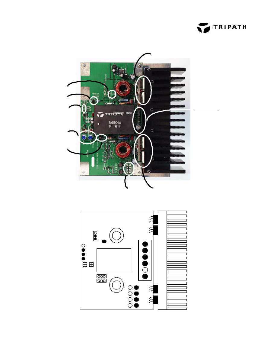
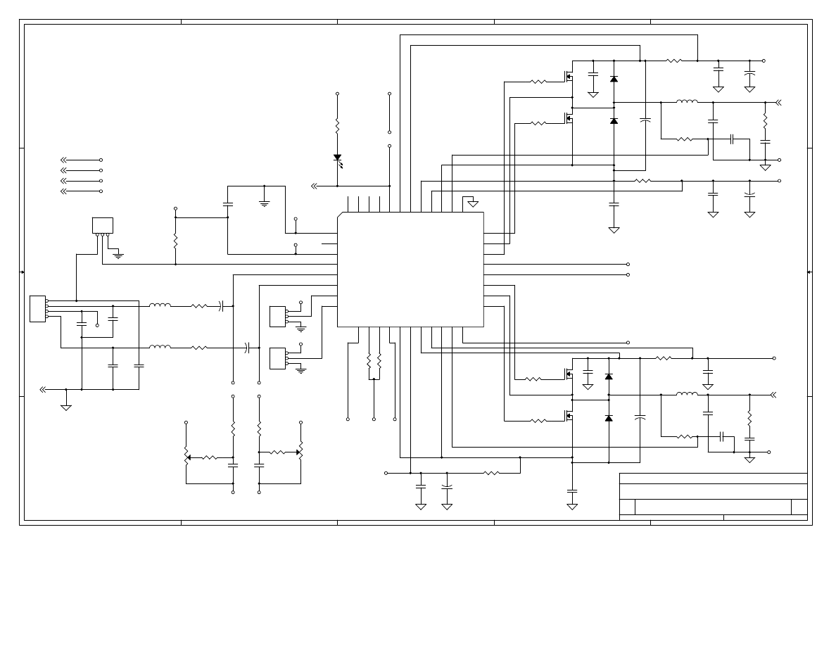
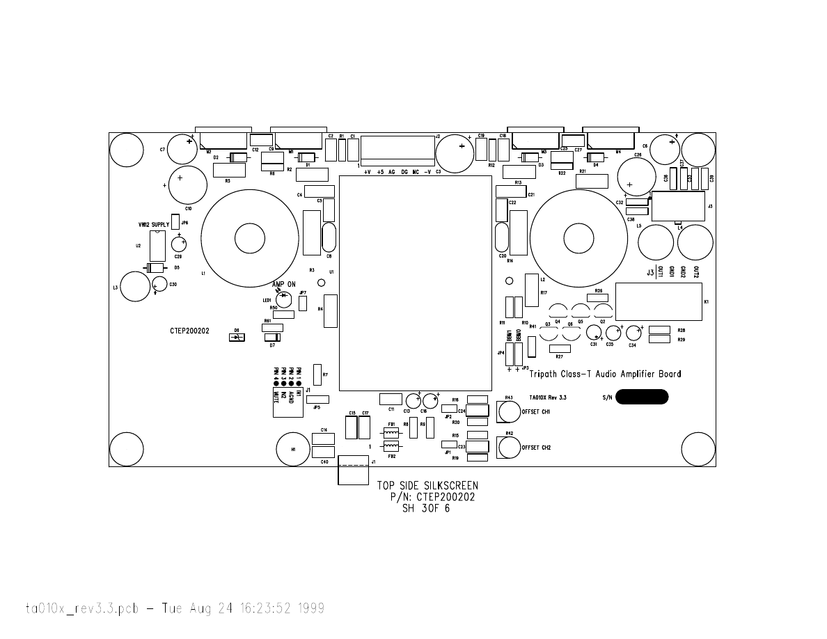
EB-TA0104 Board
Figure 1
*Please note the Break-Before-Make labels on the PC Board are incorrect and are reversed.
Figure 2
TA0104A
+V
+5
AG
DG
-V
NC
HEATSINK
MUTE
AGND
IN1
IN2
OUT1
GND1
GND2
OUT2
Tripath Class-T Audio
Amplifier Board
EB-TA0104, Rev. 3.3
LED
OFFSET CH1
OFFSET CH2
MUTE
N-Channel
MOSFETs, M1-M4
M1
M2
M3
M4
BBM0 BBM1BBM0 BBM1
+
+
Output Transistors
Output Transistors
CONNECTIONS
Vspos (+V)
+5V
AGND
DGND
NC
Vsneg (-V)
Output
Connections
Input
Connections
Mute
Jumper
Power
LED
Voltage Offset
Adjust
Break Before
Make Jumpers
T E C H N I C A L I N F O R M A T I O N
EB-TA0104, 01.01 Rev. 4.2
5
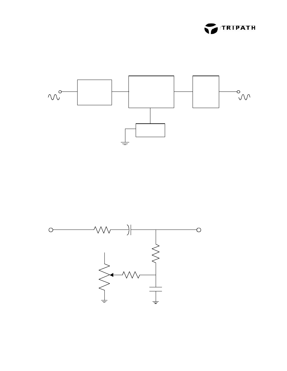
ARCHITECTURE
A block diagram of one channel of the evaluation board is shown in Figure 3. The major functional
blocks of the amplifier are described below.
Figure 3
Note: The TA0104A is an inverting amplifier.
Input Stage
Figure 4 shows one channel of the Input Stage. The TA0104A amplifier is designed to accept
unbalanced inputs and provide an overall gain of 14.5, or approximately 23 dB. Please note that the
input stage of the TA0104A is biased at approximately 2.5VDC. Therefore, for an input signal centered
around ground (0VDC), the polarity of the coupling capacitor, C
IN
, shown in Figure 4 is correct.
Figure 4
TA0104A
Output
Section
VN12
Out
Input Stage
In
+5V
1M
Ω
10K
Ω
0.1uF, 50V
1M
Ω
49.9K
Ω
1uF, 6.3V
Input to TA0104A
R
IN
C
IN
+
(DC Bias ~2.5V)
T E C H N I C A L I N F O R M A T I O N
6 EB-TA0104, 01.01 Rev. 4.2
The gain of each channel of the TA0104A amplifier is set by the value of resistor R
IN
in Figure 4 (labeled
R8 and R9 on the schematic), according to the following equation:
Av = 800 x 10
3
/ (R
IN
+ 5000)
where R
IN
is in Ohms
In this design, R
IN
is 49.9K
Ω
, which yields an Av of 14.5 (23 dB). This value is a good compromise
between gain and noise, though reducing R
IN
by a factor of two will only increase the noise generated
inside the TA0104A by ~1 dB.
The value of the input capacitor, C
IN
, in Figure 4 (labeled C13 and C16 on the schematic), and the input
resistor, R
IN
(labeled R8 and R9), set the –3dB point of the input high-pass filter. The frequency of the
input high pass pole, F
P
, –3dB point can be calculated as follows:
F
P
= 1/((2
π
x C
IN
)(R
IN
+ 5000))
where: C
IN
= input capacitor value in Farads
R
IN
= input resistor value in Ohms
Output offset voltages can be nulled by adjusting the 10K
Ω
potentiometer shown in Figure 4. Once set,
the offset does not typically drift with temperature, so no tracking circuitry is required. Offsets can
typically be set to +/- 25 mV. R43 is used to adjust the offset of CH1, and R42 is used to adjust the
offset of CH2. If a different TA0104A is placed in the EB-TA0104 evaluation board, the offset of each
channel would need to be re-trimmed.
TA0104A Control Circuitry
The 5V supply drives the power light, LED 1, directly to indicate a “good” status. If the LED 1 is off, the
amplifier is in HMUTE (see Figure 5). HMUTE goes high (i.e. LED1 is off), when a fault condition occurs.
If this is caused by an overcurrent condition, the mute pin must be cycled (i.e. low to high to low) to clear
the fault. If the fault was caused by an over- or undervoltage, simply bring the supply rails to within the
OV and UV specifications for the TA0104A (+55V to +92V). Once the supply is within these limits, the
amplifier will automatically reset and LED 1 will illuminate. As stated previously, until the supplies Vspos
and Vsneg are within the specified range, LED 1 will be illuminated. It would be impossible for the
TA0104A to report a supply voltage fault during power up without requiring a specified supply voltage
power sequence that is clearly undesirable.
The MUTE pin is brought out to an external 3-pin header, JP5 (Figure 5). When a jumper is installed
from Pin 4 to ground (by shorting pins 2 and 3 on JP5), the MUTE line is pulled to ground and the
outputs are enabled. Note that if the MUTE jumper is removed, the MUTE pin floats high, the amplifier is
muted and the power LED will not be lit. This is done to remind the user of a possible “jumper off”
condition if there is no output. If the MUTE jumper is driven from the external MUTE connection to Pin 4
and left floating, the outputs are muted.
Figure 5
+5V
LED 1
HMUTE
35
BBM0
BBM1
+5V
+5V
JP3
JP4
7
8
JP5
MUTE
MUTE
IN2
IN1
AGND
4
Pin 4
AGND
MUTE
OCR2
OCR1
R10
R11
R
OCR
10
11
T E C H N I C A L I N F O R M A T I O N
EB-TA0104, 01.01 Rev. 4.2
7
The resistors, R
OCR
in Figure 5 (labeled R10 and R11 in the schematic), set the overcurrent threshold for
the output devices. Note that these are NOT the sense resistors (the overcurrent sense resistors, R
S
,
are in the output stage). By adjusting the R
OCR
resistor values, the threshold at which the amplifier “trips”
can be changed. The range that the overcurrent trip point can be adjusted (by changing R
OCR
) is
determined by the value of the sense resistors.
R
OCR
on this evaluation board is pre-set to 10K
Ω
for a 4
Ω
application. For lower impedance applications
(i.e. 4
Ω
bridged), this board’s overcurrent may trip prematurely. This is indicated by HMUTE going high;
to clear, toggle the mute or cycle the power. To reduce overcurrent sensitivity, decrease the value of
R
OCR
until the sensitivity meets the desired level. R
OCR
can be reduced to 0
Ω
though this may result in
an overcurrent threshold that is so high the amplifier will try to drive a short circuit, possibly damaging the
output FETs.
Finally, the Break-Before-Make (or “BBM”) lines are used to control the “dead time” of the output FETs.
The “dead time” is the period of time between the turn-off of one device and the turn-on of the opposite
device on the same channel. If the two devices are both on at the same time, current “shoots through”
from one supply to the other, bypassing the load altogether. Obviously, this will have a great impact on
the overall efficiency of the amplifier. However, if the dead time is too long, linearity suffers. The
optimum BBM setting will change with different output FETs, different operating voltages, different
layouts and different performance requirements. For this reason, Tripath has provided a means to adjust
the BBM setting among four preset levels by moving jumpers JP3 and JP4 on their 3-pin headers (see
Figure 5).
These settings should be verified over the full temperature and load range of the application to ensure
that any thermal rise of the output FETs and TA0104A does not impact the performance of the amplifier.
This amplifier board is set to 65nS, and the table below shows the BBM values for various settings of the
jumpers (Figure 6).
BBM1
BBM0
Delay
1)
0
0
145nS
2)
0
1
105nS
3)
1
0
65nS
4)
1
1
25nS
Figure 6
"0"
BBM0
+
JUMPER
JP3
BBM1
+
JUMPER
"1"
JP4
(board labeled BBM0)
(board labeled BBM1)
T E C H N I C A L I N F O R M A T I O N
8 EB-TA0104, 01.01 Rev. 4.2
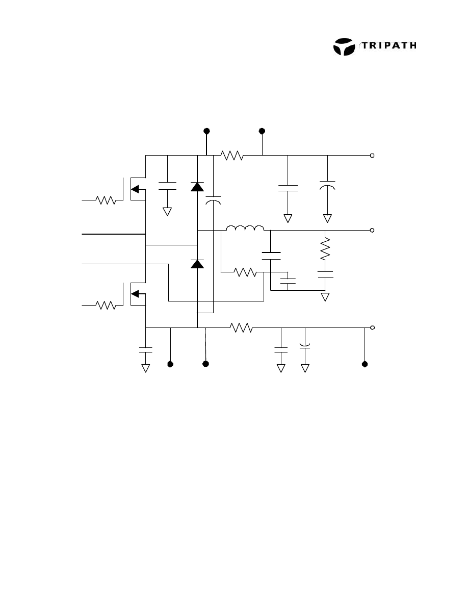
Output Section
The output section includes the gate resistors, FETs, output filters, the previously mentioned
OVERCURRENT sense resistors, clamping diodes, a Zobel Network, and various bypass capacitors.
Figure 7
The gate resistors (labeled R2, R5, R13, and R21 in the schematic and Figure 7) are used to control
MOSFET switching rise/fall times and thereby minimize voltage overshoots. They also dissipate a
portion of the power resulting from moving the gate charge each time the MOSFET is switched. If R
G
is
too small, excessive heat can be generated in the driver. Large gate resistors lead to slower gate
transitions resulting in longer rise/fall times and thus requiring a larger BBM setting. Tripath
recommends using an R
G
of 10
Ω
when the gate charge (Qg) of the output FET is less than 70nC and
5.6
Ω
when the Qg is greater than 70nC.
The output FETs, M1-M4, provide the switching function required of a Class-T design. They are driven
directly by the TA0104A through the gate resistors. The devices used on the evaluation board are ST
STW38NB20 MOSFETs. The TA0104A data sheet contains information on output FET selection as well
as Tripath application notes “FETs – Selection and Efficiency” and “Designing with Switching Amplifiers
for Performance and Reliability”.
R2/13
5.6
Ω
R5/21
5.6
Ω
LO
M2/4
HOCOM
FDBK
M1/3
HO
C2/18
0.1uF, 100v
C1/19
0.1uF, 100v
C4/21
0.22uF, 100v
C12/27
0.1uF, 100v
C9/25
0.1uF, 100v
C10/26
100uF, 100V
R6/22 0.01
Ω
R1/12 0.01
Ω
L1/2
11.3uH
C3
100uF, 100v
C5/22
0.1uF, 100v
R3/14 33
Ω
D2/4
D1/3
OCSH+
OCSH-
OCSL-
OCSL+
VSNEG
OUT
VSPOS
R4/17 1K
Ω
C8/20
50pF, 100v
C6/7, NS
LOCOM

T E C H N I C A L I N F O R M A T I O N
EB-TA0104, 01.01 Rev. 4.2
9
The output filters L1/C4 and L2/C21 are the low-pass filters that recover the analog audio signal. One of
the benefits of the Class-T design is the ability to use output filters with relatively high cutoff frequencies.
This greatly reduces the speaker interactions that can occur with the use of lower-frequency filters
common in Class-D designs. Also, the higher-frequency operation means that the filter can be of a
lower order (simpler and less costly).
The OEM may benefit from some experimentation in the filter design, but the values provided in the
reference design, 11.3uH and 0.22uF, provide excellent results for most loads between 4
Ω
and 8
Ω
.
As important as the values themselves, the material used in the core is important to the performance of
the filter. Core materials that saturates too easily will not provide acceptable distortion or efficiency
figures. Tripath recommends a low-mu (permeability of 10) type 2 iron powder core.
The clamping diodes D1-D4 are required to limit the reverse voltages seen by the output FETs as a
result of normal operation. The diodes should be mounted as close as possible to the FET. Depending
on the application, these may or may not be necessary.
The Zobel circuits R3/C5 and R14/C22 are there in case an amplifier is powered up with no load
attached. The Q of the LC output filter, with no load attached, rises quickly out to 80kHz. Resonant
currents in the filter and ringing on the output could reduce the reliability of the amplifier. The Zobel
eliminates these problems by reducing the Q of the network significantly above 50kHz. Modifying the LC
output filter should not require a recalculation of the Zobel value.
The bypass capacitors C12/C27 are critical to the reduction of ringing on the outputs of the FETs. These
parts are placed as closely as possible to the leads of the FETs, and the leads of the capacitors
themselves are as short as practical. Their values will not change with different output FETs.
T E C H N I C A L I N F O R M A T I O N
10 EB-TA0104, 01.01 Rev. 4.2
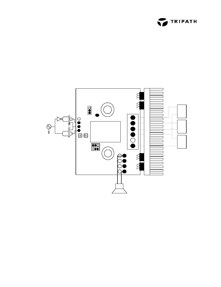
Connection Diagram for Bridge Mode Operation
The amplifier is connected to the power supplies and load as shown in Figure 8. Note that an inverter
has been added in front of one of the channel inputs (i.e. channel 2). The main reason for processing
the channels out of phase is to avoid potential problems with switching power supplies, but it also
simplifies the connections for bridged-mode operation. For bridged operation, simply connect the “-“
terminal to the output of the inverted channel (i.e. channel 1) and the “+” terminal to the output of the
non-inverted channel with respect to the input signal (i.e. channel 2). As stated before, the TA0104A is
an inverting amplifier.
*Please note the Break-Before-Make labels on the PC Board are incorrect and are reversed.
Figure 8
70V
+
-
70V
+
-
5V
+ -
Bridged
Subwoofer
.
.
.
AGND
Audio
Input
RCA
+
RCA
+
+ -
TA0104A
BBM0 BBM1
+
+
+V
+5
AG
DG
-V
NC
MUTE
AGND
IN1
IN2
Tripath Class-T Audio
Amplifier Board
EB-TA0104, Rev. 3.3
LED
OFFSET CH1
OFFSET CH2
MUTE
N-Channel
MOSFETs, M1-M4
M1
M2
M3
M4
OUT1
GND1
GND2
OUT2
HEATSINK
T E C H N I C A L I N F O R M A T I O N
EB-TA0104, 01.01 Rev. 4.2
11
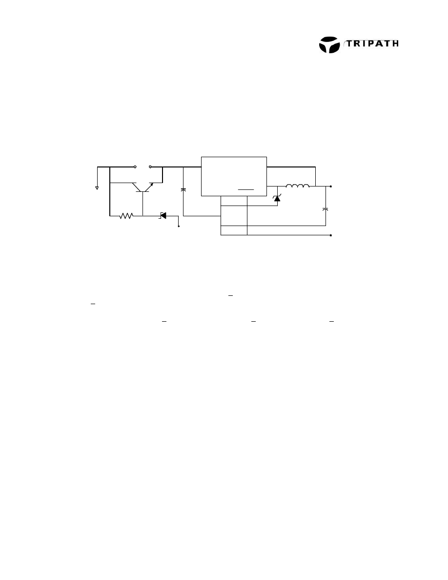
VN12 Bias Requirement
The VN12 circuit (Figure 9) is used to provide the voltage rail for the low side FET drivers on the
TA0104A. This supply must track the Vsneg rail, and so, for simplicity, this supply is included on this
amplifier board. The VN12 circuit uses a National LM2594HVN-12 “simple switcher” voltage regulator
for all control. A few passive components complete the design. Tripath does not anticipate that there
will be any reason to modify the operation of this circuit. Should the OEM wish to do so, however,
reference data for the LM2594 is available at www.national.com/pf/LM/LM2594.
Figure 9
FAQ’s
Q. The TA0104A supply voltage rails are rated at +100V. Why is this evaluation board limited
to +90V maximum?
A. IC’s used in the 12V bias supply circuitry as well as the choice of STW38NB20 FETs limit this
boards voltage supply to +90V into 4
Ω
single ended, +75V for 4
Ω
Bridged, or +75V for 2
Ω
single
ended applications. Damage will occur to the board at higher voltages.
Q. Can I use the TA0104A reference design to drive 2
Ω
(or lower) loads?
A. The reference design can drive 2
Ω
single ended loads. For use with loads of lower nominal
impedance, a new filter design may be required. Please contact the Tripath Applications group for
support in this area.
Q. Do I need to attach a fan to the heat sink?
A. For normal operation, the heatsink is sized appropriately. Continuous operation at high levels
(especially low impedance loads) may cause excessive power dissipation thus requiring a fan.
DOCUMENTATION
Schematics and layout in software or paper form can be provided upon request.
CONTACT INFORMATION
For more information on Tripath products, visit our web site at:
www.tripath.com
TRIPATH TECHNOLOGY, INC.
3900 Freedom Circle, Suite 200
Santa Clara, California 95054
408-567-3000
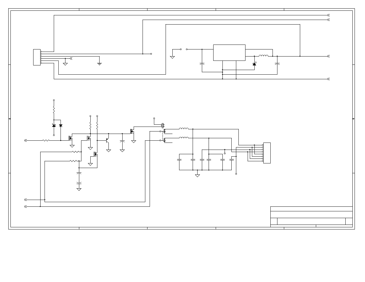
LM2594HVN-12
VSNEG
VN12
1000uF
100uH
10uF
JP6
C29
D5
L3
C30
+VIN
GND
OUT
FB
ON/OFF
NS
VSNEG
D8
R44
10K
Ω
Q1
U2
5
5
4
4
3
3
2
2
1
1
D
D
C
C
B
B
A
A
From
Preamp
Board
GND1
EB-TA0104
3.3F3
EB-TA0104 2CH AUDIO AMPLIFIER BOARD
B
2
3
Tuesday, January 16, 2001
Title
Size
Document Number
Rev
Date:
Sheet
of
VP75B
OUT2
COM2
COM1
VP75A
OUT1
OUT2
VSPOS
VSNEG
VN12REF
V5
HMUTE
GPWR
Pin3V5
VSNEG
VSPOS
V5
Pin3V5
VSPOS
V5
V5
VSNEG
AGND
VSNEG
VSPOS
VN12REF
VSPOS
VSNEG
VN12REF
V5
GND_2
GND_1
GND_2
AGND
AGND
AGND
AGND
Pin3V5
V5
V5
GND_1
R4
1K
1W
5%
C8
47PF
500V
10%
R21
5.6
1W
5%
R13
5.6
1W
5%
FB1
EXC-ELSA35
C14
NS
1
2
FB2
EXC-ELSA35
+
C6
NS
+
C7
NS
C24
0.1UF
50V
5%
JP2
2-pin Header
0.100"
R12
1W
0.01
1%
D4
MUR120
D3
MUR120
R50
2K
0.25W
5%
LED1
AMP ON (GREEN LED)
2
1
JP7
NS
C18
0.1UF
100V
5%
R22
1W
0.01
1%
L2
11.3UH
10A
10%
C21
0.22UF
100V
5%
C22
0.1UF
100V
5%
R14
33
2W
5%
C27
0.1UF
100V
5%
R8
49.9K
0.25W
1%
C12
0.1UF
100V
5%
R17
1K
1W
5%
C20
47PF
500V
10%
C25
0.1UF
100V
5%
+
C26
100UF
100V
20%
R15
1M
0.25W
5%
R9
49.9K
0.25W
1%
R20
1M
0.25W
5%
C11
0.1UF
50V
5%
C19
0.1UF
100V
5%
JP3
3-pin Header
0.100"
1
2
3
R11
10K
0.25W
5%
R10
10K
0.25W
5%
JP4
3-pin Header
0.100"
1
2
3
R43
10K
Single Turn
1
3
2
R42
10K
Single Turn
1
3
2
+
C13
1UF
50V
20%
+
C16
1UF
50V
20%
R7
10K
0.25W
5%
J1
4-Terminals
1
2
3
4
R19
1M
0.25W
5%
C23
0.1UF
50V
5%
C17
NS
1
2
U1
TA0104
1
2
3
4
5
6
7
8
9
10
11
12
13
14
15
16
17
18
19
20
21
22
23
24
25
26
27
28
29
30
31
32
33
34
35
36
37
38
39
AGND
OVERLOAD
V5
MUTE
IN2
IN1
BBM0
BBM1
GNDKELVIN1
OCR2
OCR1
GNDKELVIN2
NSNS1N
NSNS1P
PSNS1N
PSNS1P
COM1
FDBKN1
VN12REF
LO1
BR1
HO1
VSPOS
VSNEG
HO2
BR2
LO2
PGND
FDBKN2
COM2
NSNS2P
NSNS2N
PSNS2N
PSNS2P
HMUTE
TEST1
TEST2
TEST3
C_GND
R16
1M
0.25W
5%
JP5
3-pin Header
0.100"
1
2
3
C40
NS
1
2
C15
NS
1
2
M2
STW38NB20
2
1
3
M1
STW38NB20
2
1
3
M3
STW38NB20
2
1
3
M4
STW38NB20
2
1
3
R2
5.6
1W
5%
JP1
2-pin Header
0.100"
L1
11.3UH
10A
10%
C2
0.1UF
100V
5%
D2
MUR120
D1
MUR120
R5
5.6
1W
5%
+
C10
100UF
100V
20%
R3
33
2W
5%
C9
0.1UF
100V
5%
C5
0.1UF
100V
5%
R1
1W
0.01
1%
R6
1W
0.01
1%
C4
0.22UF
100V
5%
+
C3
100UF
100V
20%
C1
0.1UF
100V
5%
5
5
4
4
3
3
2
2
1
1
D
D
C
C
B
B
A
A
Tie pins 1, 2, 3 to VSNEG
(pins 5, 6).
The relay will not be stuffed.
Please short pin 5 to pin 7 and
pin 6 to pin 8 with bare 18AWG
wires. This allows the signal
to bypass the relay.
EB-TA0104
3.3F3
EB-TA0104 2CH AUDIO AMPLIFIER BOARD
B
3
3
Tuesday, January 16, 2001
Title
Size
Document Number
Rev
Date:
Sheet
of
OUT1
OUT2
HMUTE
VN12REF
VSNEG
V5
VSPOS
GPWR
V5
V5
V5
V5
GND_1
GND_2
V5
VSNEG
R27
NS
R28
NS
+
C35
NS
R29
NS
+
C31
NS
+
C34
NS
Q5
NS
2
3
1
K1
NS
6
4
8
5
3
7
2
1
Q4
NS
2
3
1
Q2
NS
2
3
1
Q6
NS
2
3
1
R26
NS
Q3
NS
2
3
1
L3
330UH
0.5A
10%
R41
NS
JP6
NS
L4
NS
L5
NS
C33
NS
C32
NS
+ C30
82UF
25V
20%
1
2
U2
LM2594HVN-12
8
6
4
5
7
OUT
GND
FB
NOT ON/OFF
+VIN
C36
NS
C39
NS
C37
NS
C38
NS
J2
4-Terminals
1
2
3
4
5
6
D5
11DQ09
R61
NS
D7
NS
D6
NS
+ C29
10UF
63V
20%
1
2
J3
6-Terminals
1
2
3
4
5
6
7
8
EB-TA0104 Bill Of Materials
Revision 8
P/N
Qty.
Reference
Description
Value
Rating
Tol.
MFG.
Mfg. Part #
Vendor
Vendor Part #
1
050-00012-0AB
1
PCB Assembly, Tested
EB-TA0104
2
040-00012-0AB
1
PCB Assembly, Untested
EB-TA0104
3
302-00001-000
10
C1,C2,C5,C9,C12,C18,C19,
C22,C25,C27
Stack Metallized Film Caps
0.1UF
100V
5%
Panasonic
ECQ-V1104JM
Digi-Key
P4725-ND
4
301-00005-000
3
C3,C10,C26
Radial Lead Aluminum Electrolytic Caps
100UF
100V
20%
Panasonic
ECA-2AHG101
Digi-Key
P5597-ND
5
302-00003-000
2
C21,C4
Stack Metallized Film Caps
0.22UF
100V
5%
Panasonic
ECQ-V1224JM
Digi-Key
P4729-ND
6
300-00008-000
2
C8,C20
Ceramic Disk Caps
47PF
500V
10%
Panasonic
E4008A-ND
Digi-Key
ECC-D2H470K5
7
302-00007-000
3
C11,C23,C24
Stack Metallized Film Caps
0.1UF
50V
5%
Panasonic
ECQ-V1H104JL
Digi-Key
P4525-ND
8
301-00017-000
2
C13,C16
Radial Lead Aluminum Electrolytic Caps
1UF
50V
20%
Panasonic
ECA-1HM010
Digi-Key
P5174-ND
9
301-00006-000
1
C29
Radial Lead Aluminum Electrolytic Caps
10UF
63V
20%
Panasonic
ECA-1JM100
Digi-Key
P5189-ND
10
301-00018-000
1
C30
Radial Lead Aluminum Electrolytic Caps
82UF
25V
20%
Panasonic
ECA-1EFQ820
Digi-Key
P5697-ND
11
400-00005-000
4
D1,D2,D3,D4
Fast Recovery Diode
200v, 1A, DO-41
200V
Motorola
MUR120
12
400-00013-000
1
D5
Schottky Diode
90v, 1A, DO-41
IR
11DQ09
Digi-Key
11DQ09-ND
13
215-00001-000
2
FB1,FB2
Ferrite Bead, 3.5x6x0.8, 60ohm,@100Mhz
EXC-ELSA35
Panasonic
EXC-ELSA35
14
800-00003-000
2
JP2,JP1
Header Strips
2-pin Header, 0.100"
Phyco
2100-1X2SF1
15
800-00016-000
3
JP3,JP4,JP5
Header Strips
3-pin Header, 0.100"
Phyco
2100-1X3SF1
16
404-00002-000
1
LED1
0.100" spacing
AMP
ON
(GREEN
LED)
open
17
700-00001-000
2
L2,L1
Iron Powder, 29 Turns of 16 AWG
11.3UH
10A
10%
Amidon
T-106-2
AMIDON
AMI-10231
18
700-00002-000
1
L3
Inductor
330UH
3A
10%
ISI
RL622-331K
19
503-00004-000
4
M1,M2,M3,M4
N-Ch Mosfet
STW38NB20
200V/38A
SGS-Thomson STW38NB20
20
206-00001-000
4
R1,R6,R12,R22
Resistor
0.01
1W
1%
Well-Mag
MR0100805
21
206-00003-000
4
R2,R5,R13,R21
Resistor, CAR
5.6
1W
5%
Panasonic
Digi-Key
P5.6W-1TR-ND
22
207-00002-000
2
R14,R3
Resistor, CAR
33
2W
5%
Panasonic
Digi-Key
P33W-2TR-ND
23
206-00004-000
2
R4,R17
Resistor, CAR
1K
1W
5%
Panasonic
Digi-Key
P1.0KW-1TR-ND
24
202-00006-000
3
R7,R10,R11
Resistor, CAR
10K
0.25W
5%
Yageo
Digi-Key
10KQTR-ND
25
202-00007-000
2
R8,R9
Resistor, CAR
49.9K
0.25W
1%
Yageo
Digi-Key
49.9XTR-ND
26
202-00008-000
4
R15,R16,R19,R20
Resistor, CAR
1M
0.25W
5%
Yageo
Digi-Key
1MQTR-ND
27
204-00008-000
2
R42,R43
Resistor
10K-Single Turn POT
Bourns
3306P-1103
Digi-Key
3306P-103-ND
28
202-00009-000
1
R50
Resistor, CAR
2K
0.25W
5%
29
050-00006-3AB
1
U1
Audio Amplifier
TA0104
Tripath,
consigned part
TA0104
30
601-00003-000
1
U2
IC, DIP 8, 3A, Step Down regulator
LM2594HVN-12
NSC
LM2594HVN-12
31
800-00017-000
2
U1
1 X 11 female socket
Phyco
4150-1X11 SF1
32
800-00018-000
2
U1
1 X 8 female socket
Phyco
4150-1X8 SF1
33
850-00003-000
1
Cable Ties
8"
T&B
10400
34
180-00003-000
1
Printed Circuit Board
Bay Area Ckt
TA010X_REV 3.3
35
850-00004-000
4
Aluminum Stand-Offs
4-40 x 0.5"
Olander
4C50RF4U
36
850-00005-000
4
Screws for Stand-Offs
4-40 x 1/4"
Olander
4C25PPMS
37
850-00006-000
4
Alumina Oxide Spacers
Thermalloy
4170
Bisco Industries
38
850-00007-000
1
Heatsink
ACK Tech/ CCI CS8157-18070
39
850-00008-000
2
Small, Clamp Bars
Abacus
100-3900-002
40
850-00009-000
2
Screws for Clamp Bars
4-40 x 1/2"
Olander
4C75PPMS
41
850-00010-000
1
Red Wire
6", 24 AWG Wire
open
42
850-00013-000
1
Red Wire
6", 18 AWG Wire
open
43
850-00013-000
1
Red Wire
12", 18 AWG Wire
open
44
850-00011-000
1
Black Wire
6", 24 AWG Wire
open
45
850-00014-000
1
Black Wire
6", 18 AWG Wire
open
46
850-00014-000
1
Black Wire
12", 18 AWG Wire
open
47
850-00012-000
1
White Wire
6", 24 AWG Wire
open
48
850-00015-000
1
White Wire
6", 18 AWG Wire
open
49
850-00016-000
1
Yellow Wire
12", 18 AWG Wire
open
50
850-00017-000
1
Blue Wire
6", 18 AWG Wire
open
51
850-00017-000
1
Blue Wire
12", 18 AWG Wire
open
52
850-00018-000
1
Orange Wire
12", 18 AWG Wire
open
53
800-00009-000
2
Female Banana Jack w/ screws
Red
Johnson Comp. 108-0901-001
Digi-Key
J151-ND
54
800-00010-000
2
Female Banana Jack w/ screws
Black
Johnson Comp. 108-0903-001
Digi-Key
J152-ND
55
800-00012-000
2
Female Banana Jack w/ screws
Blue
Johnson Comp. 108-0910-001
Digi-Key
J155-ND
56
800-00011-000
1
Female Banana Jack w/ screws
White
Johnson Comp. 108-0901-001
Digi-Key
J150-ND
57
800-00014-000
1
Female Banana Jack w/ screws
Yellow
Johnson Comp. 108-0907-001
Digi-Key
J154-ND
58
800-00013-000
1
Female Banana Jack w/ screws
Orange
Johnson Comp. 108-0906-001
Digi-Key
J356-ND
59
33
K1,Q2,Q3,Q4,Q5,Q6,D6,C6,JP7,D7,C
7,C14,C15,C17,L4,L5,R26,R27,R28,R
29,C31,
C32,C33,C34,C35,C36,C37,C38,C39,
C40,R41,R61, JP6
NS
60
850-00019-000
6
8-32 x 3/8 Phil Flat, Baseplate screw, SS
open
Orlander
61
850-00020-000
4
4-40 x 1/4 Phil Flat, Baseplate screw, SS
open
Orlander
62
850-00021-000
1
Baseplate, Aluminum
American
Tooling
TA0103, 04 baseplate
63
400-00014-000
1
JP6
Zener Diode, 51v, 1w
1N4757
open
64
503-00005-000
1
JP6
MOSFET, NPN, TO-220
2N5494
50v
open
65
202-00006-000
1
JP6
Resistor
10K ohm
.25w
5%
Yageo
Digi-Key
10KQTR-ND
66
850-00022-000
1
JP6
Heatsink, TO-220
open
67
800-00019-000
5
JP1, JP2, JP3, JP4, JP5
Jumper Headers, 2 pin
open
68
950-00003-000
1
Shipping box w/ foam
69
950-00004-000
1
10 x 12 Anti-static bag
70
850-00031-000
1
JP6
Nut, #6 hex
71
850-00032-000
1
JP6
Screw, #6 x 1/4", Pan Hd, PH
Special Instructions
Note #1 (J1):
Use a 24AWG (6" long) stripped at end, 1/4" expose wire leads
Terminal 1: Red Wire
Terminal 2: Black Wire
Terminal 3: White Wire
Terminal 4: No Wire
Note #2 (J2):
Use a 18AWG (12" long) terminate with same color female banana jack at the end.
Terminal 1: Yellow Wire
Terminal 2: Red Wire
Terminal 3: Black Wire
Terminal 4: Blue Wire
Terminal 5: No wire
Terminal 6: Orange Wire
Note #3 (J3):
Use a 18AWG (6" long) terminate with same color female banana jack at the end.
Terminal 1: Red Wire
Terminal 2: Black Wire
Terminal 3: Blue Wire
Terminal 4: White Wire
Note #4:
Use 18 gauge wire-uninsulated, jumper L4 and L5
Use 18 gauge wire uninsulated, jumper K1 location (pins 5 to pin 7 and pins 6 to pin 8)
Note #5:
Install Header Jumpers at locations: JP1, JP2, JP3, JP4, JP5
(refer to sample for orientation)
Note #6:
JP6, refer to sample for installation/orientation of components
Wyszukiwarka
Podobne podstrony:
1b Water Hygiene Amended EB
4) EB II Strategia lizbońska, WSE notatki
MSP PRZEWODNIK 10 11 ZI ĘBA
a Mat inf. dz.wykl 11 , 1 „Równowaga przeżywania"(EB=Experience Balance)
a Mat inf. dz.wykl 9 , 1 „Równowaga przeżywania"(EB=Experience Balance)
a Mat inf. dz.wykl 14, 1 „Równowaga przeżywania"(EB=Experience Balance)
EB 2013, oszustwa i naduzycia ss portal
WSHiP SZTUKA ARGUMENTACJI eb 2008 WYDRUKOWANE
Kopia WSEI ZN BADANIE I ANALIZA eb 2008
Marsz żałobny, Marsz żałobny Alto Horn in Eb 1
EB wyklad, Administracja, I ROK, Etyka
Kopia WSEI ZN BADANIE I ANALIZA eb 2008
Marsz żałobny Marsz żałobny Alto Horn in Eb 1
EB 2013 ss, przedsiebiorstwo a pracownicy portal
a Mat inf. dz.wykl 10 , 1 „Równowaga przeżywania"(EB=Experience Balance)
1)+EB+Korporacje+transnarodowe+w+procesie+globalizacji, międzynarodowe stosunki finansowe
10 In field Test Equipment Methods linked with 1a EB
więcej podobnych podstron