Order this document
by BR774/D
© MOTOROLA INC., 1991, 1997
This document contains information on a new product. Specifications and information herein are subject to change without notice.
MOTOROLA
SEMICONDUCTOR
TECHNICAL DATA
MC68HC11L6
Technical Summary
8-Bit Microcontroller
1 Introduction
The design of the MC68HC11L6 high-performance microcontroller (MCU) is based on the
MC68HC11E9, and includes 16 Kbytes of ROM and an additional bidirectional port (port G). The
MC68HC11L6 is a high-speed, low-power chip with a multiplexed bus capable of operating at up to 3
MHz. The fully static design allows it to operate at frequencies down to dc.
This summary of technical information is organized into sections, each containing a short description
and block diagram of a subsystem and its registers. The bit descriptions included describe only those
bits specific to the particular subsystem. For more detailed information on subsystems, programming,
and the instruction set,
refer to the
M68HC11 Reference Manual
(M68HC11RM/AD).
2 Features
• M68HC11 CPU
• Power-Saving STOP and WAIT Modes
• 16 Kbytes of ROM
• 512 Bytes of On-Chip Electrically Erasable PROM (EEPROM) Security
• 512 Bytes of On-Chip RAM (All Saved During Standby)
• 16-Bit Timer System
— Four Output Compare Channels
— Three Input Capture Channels
— One Input Capture or Output Compare (Software Selectable)
• 8-Bit Pulse Accumulator
• Real-Time Interrupt Circuit
• Computer Operating Properly (COP) Watchdog System
• Synchronous Serial Peripheral Interface (SPI)
• Asynchronous Nonreturn to Zero (NRZ) Serial Communications Interface (SCI)
• Eight-Channel 8-Bit Analog-to-Digital (A/D) Converter
• 46 General-Purpose I/O Pins
— 24 Bidirectional Input/Output (I/O) Pins
— 11 Input-Only and 11 Output-Only Pins
• Available in a 64-Pin Surface Mount Quad Flat Pack or a 68-Pin Plastic Leaded Chip Carrier
Table 1 Ordering Information
Package
Temperature
CONFIG
Description
MC Order Number
PLCC (FN suffix)
– 40
°
to + 85
°
C
$0F
BUFFALO ROM
MC68HC11L6FN1
QFP (FU Suffix)
– 40
°
to + 85
°
C
$0F
BUFFALO ROM
MC68HC11L6VFU1

Section
Page
MOTOROLA
MC68HC11L6
2
BR774/D
Operating Modes and Memory Maps
........................................................................... 6
Electrically Erasable Programmable Read-Only Memory (EEPROM)
Serial Communications Interface (SCI)
..................................................................... 24
Serial Peripheral Interface (SPI)
................................................................................... 30
TABLE OF CONTENTS
MC68HC11L6
MOTOROLA
BR774/D
3
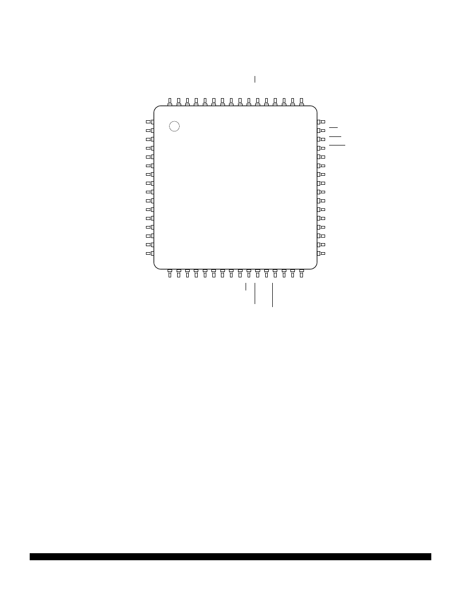
Figure 1 64-Pin Quad Flat Pack (QFP) Pin Assignments
14
15
1
2
3
4
5
6
7
8
9
33
47
46
45
44
43
42
41
40
39
38
10
11
12
13
37
36
35
34
16
48
PE1/AN1
PE5/AN5
PB0/ADDR8
PB1/ADDR9
PB2/ADDR10
PB3/ADDR11
PB4/ADDR12
PB5/ADDR13
PB6/ADDR14
PB7/ADDR15
PG5
PG4
PG6
PG7
PE0/AN0
PE4/AN4
PC2/ADDR2/DATA2
PC5/ADDR5/DATA5
PC4/ADDR4/DATA4
PC3/ADDR3/DATA3
PC1/ADDR1/DATA1
PC0/ADDR0/DATA0
PD0/RxD
IRQ
XIRQ
RESET
PG0
PG1
PG2
PG3
PC7/ADDR7/DATA7
PC6/ADDR6/DATA6
61
60
59
58
57
54
55
52
51
50
49
63
62
53
64
PA4/OC4/OC1
PA6/OC2/OC1
PA5/OC3/OC1
V
SS
PA2/IC1
PA1/IC2
PA7/PAI/OC1
PA3/OC5/IC4/OC1
PA0/IC3
PD4/SCK
PD3/MOSI
PD2/MISO
PD1/TxD
V
SS
V
DD
PD5/SS
24
25
26
27
28
29
17
18
19
20
21
22
23
30
31
32
PE2/AN2
V
RL
PE6/AN6
V
RH
PE7/AN7
PE3/AN3
AV
DD
E
STRA/AS
MODA/LIR
MODB/V
STBY
V
SS
STRB/R/
W
EXTAL
XTAL
V
DD
56
MC68HC11L6
MOTOROLA
MC68HC11L6
4
BR774/D
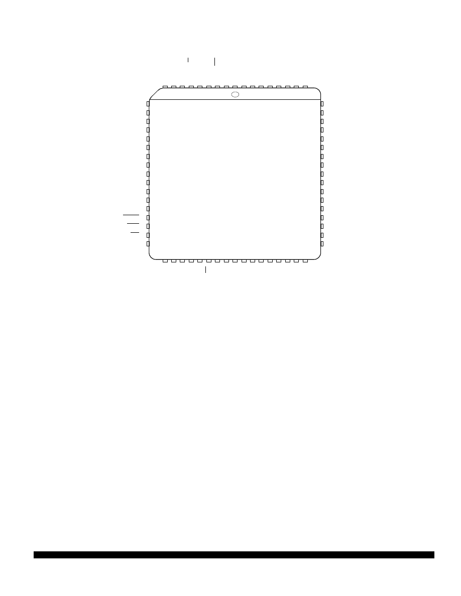
Figure 2 68-Pin Plastic-Leaded Chip Carrier (PLCC) Pin Assignments
MODA/LIR
V
SS
MODB/V
STBY
XTAL
E
STRB/R/W
V
SS
STRA/AS
EXTAL
V
RL
PE7/AN7
PE3/AN3
PE6/AN6
PE2/AN2
AV
DD
V
RH
23
24
10
11
12
13
14
15
16
17
18
45
59
58
57
56
55
54
53
52
51
50
19
20
21
22
49
48
47
46
25
60
XIRQ
IRQ
PC6/ADDR6/DATA6
PC5/ADDR5/DATA5
PC4/ADDR4/DATA4
PC3/ADDR3/DATA3
PC2/ADDR2/DATA2
PC1/ADDR1/DATA1
PC0/ADDR0/DATA0
V
DD
PG3
PC7/ADDR7/DATA7
PG2
PG1
PG0
RESET
PB5/ADDR13
PB2/ADDR10
PB3/ADDR11
PB4/ADDR12
PB6/ADDR14
PB7/ADDR15
PE5/AN5
PE1/AN1
PE4/AN4
PE0/AN0
PG7
PG6
PG5
PG4
PB0/ADDR8
PB1/ADDR9
6
5
4
3
2
67
68
65
64
63
62
8
7
66
9
34
35
36
37
38
39
27
28
29
30
31
32
33
40
41
42
V
SS
PD4/SCK
PD1/TxD
PD5/SS
PD3/MOSI
PD2/MISO
V
DD
PA4/OC4/OC1
PA5/OC3/OC1
PA6/OC2/OC1
PA7/PAI/OC1
V
DD
PA3/OC5/IC4/OC1
PA2/IC1
PA1/IC2
PA0/IC3
MC68HC11L6
61
44
V
SS
PD0/RxD
26
EXTAL
43
1
NC
MC68HC11L6
MOTOROLA
BR774/D
5
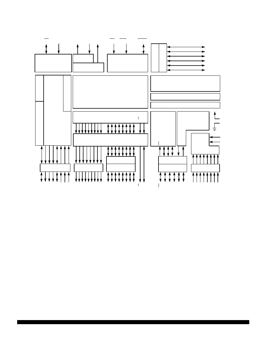
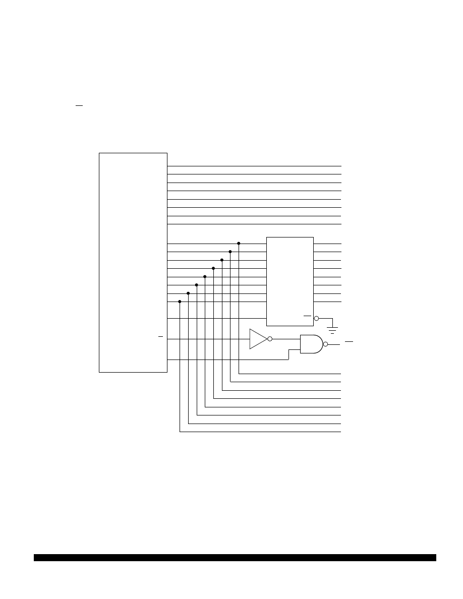
Figure 3 Block Diagram
L6 BLOCK
PC7/ADDR7/DATA7
PC6/ADDR6/DATA6
PC5/ADDR5/DATA5
PC4/ADDR4/DATA4
PC3/ADDR3/DATA3
PC2/ADDR2/DATA2
PC1/ADDR1/DATA1
PC0/ADDR0/DATA0
MODE CONTROL
OSC
CLOCK LOGIC
INTERRUPT
LOGIC
512 BYTES EEPROM
512 BYTES RAM
SERIAL
PERIPHERAL
INTERFACE
SPI
SERIAL
COMMUNICATION
INTERFACE
SCI
M68HC11 CPU
A/D CONVERTER
CONTROL
PORT D
PORT E
PE7/AN7
TxD
RxD
SS
SCK
MOSI
MISO
PD5/SS
PD0/RxD
STRA/AS
STRB/R/W
ADDRESS/DATA
BUS EXPANSION
ADDRESS
AS
STROBE AND HANDSHAKE
PARALLEL I/O
STRB
STRA
CONTROL
PORT C
PORT B
PB7/ADDR15
PORT A
PA7/PAI
TIMER
SYSTEM
COP
PULSE ACCUMULATOR
OC2
OC3
OC4
OC5/IC4/OC1
IC1
IC2
IC3
PAI
PERIODIC INTERRUPT
MODA/
LIR
MODB/
V
STBY
XTAL
EXTAL
E
IRQ
XIRQ/V
PPE
RESET
PD4/SCK
PD3/MOSI
PD2/MISO
PD1/TxD
R/W
PA6/OC2/OC1
PA5/OC3/OC1
PA4/OC4/OC1
PA3/OC5/IC4/OC1
PA2/IC1
PA1/IC2
PA0/IC3
PB6/ADDR14
PB5/ADDR13
PB4/ADDR12
PB3/ADDR11
PB2/ADDR10
PB1/ADDR9
PB0/ADDR8
PE6/AN6
PE5/AN5
PE4/AN4
PE3/AN3
PE2/AN2
PE1/AN1
PE0/AN0
V
DD
V
SS
V
RH
V
RL
16 KBYTES EPROM/OTPROM
CONTROL
PORT D
PG5
PG0
PG4
PG3
PG2
PG1
MOTOROLA
MC68HC11L6
6
BR774/D
3 Operating Modes and Memory Maps
In single-chip operating mode, the MC68HC11L6 is a monolithic microcontroller without external ad-
dress or data buses.
In expanded multiplexed operating mode, the MCU can access a 64 Kbyte address space. The space
includes the same on-chip memory addresses used for single-chip mode, in addition to external periph-
eral and memory devices. The expansion bus is made up of ports B and C, and control signals AS and
R/W. The address, R/W, and AS signals are active and valid for all bus cycles, including accesses to
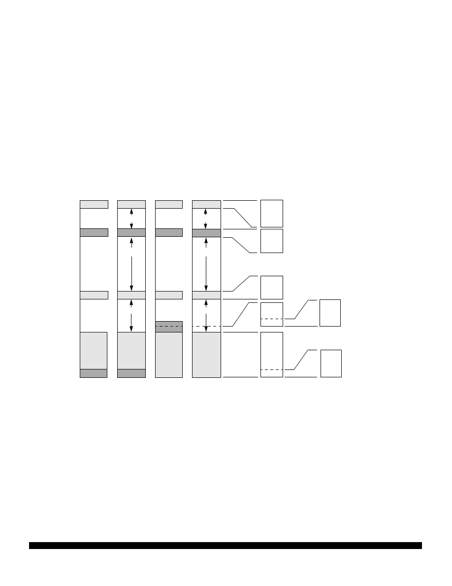
internal memory locations. The following figure demonstrates a recommended method of demultiplex-
ing low-order addresses from data at port C.
Figure 4 Address/Data Demultiplexing
The special bootstrap mode allows unlimited special purpose programs to be entered into internal RAM.
The boot loader program uses the SCI to read a program of up to 512 bytes into on-chip RAM at $0000
through $01FF. After a four-character delay, or receiving the character for address $01FF, control pass-
es to the loaded program at $0000.
Special test mode is used primarily for factory testing.
PB7
PB6
PB5
PB4
PB3
PB2
PB1
PB0
PC7
PC6
PC5
PC4
PC3
PC2
PC1
PC0
DATA1
DATA2
DATA3
DATA4
DATA5
DATA6
DATA7
DATA8
LE
Q1
Q2
Q3
Q4
Q5
Q6
Q7
Q8
OE
ADDR7
ADDR6
ADDR5
ADDR4
ADDR3
ADDR2
ADDR1
ADDR0
R/W
E
WE
ADDR15
ADDR14
ADDR13
ADDR12
ADDR11
ADDR10
ADDR9
ADDR8
MC54/74HC373
DATA7
DATA6
DATA5
DATA4
DATA3
DATA2
DATA1
DATA0
AS
MC68HC11L6
MC68HC11L6
MOTOROLA
BR774/D
7
3.1 Memory Maps
Memory locations are the same for expanded multiplexed and single-chip modes. The 64-byte register
block originates at $1000 after reset and can be placed at any other 4K boundary ($x000) after reset by
writing an appropriate value to the INIT register. The on-board 512-byte RAM is located at $0000 after
reset and can be placed at any other 4K boundary ($x000) by writing an appropriate value to the INIT
register. The 512-byte EEPROM is located at $B600 through $B7FF after reset, if it is enabled. The 16
Kbyte ROM is located at $C000 through $FFFF, if it is enabled.
Hardware priority is built into the memory remapping. Registers have priority over RAM, and RAM has
priority over ROM. The higher priority resource covers the lower, making the underlying locations inac-
cessible.
In special bootstrap mode, a bootloader ROM is enabled at locations $BF40 through $BFFF.
In special test mode and special bootstrap mode, reset and interrupt vectors are located at $BFC0
through $BFFF.
Figure 5 MC68HC11L6 Memory Map
FFC0
FFFF
NORMAL
MODES
INTERRUPT
VECTORS
64-BYTE REGISTER BLOCK
512 BYTES RAM
SINGLE
CHIP
BOOTSTRAP
SPECIAL
TEST
EXT
$0000
$1000
$B600
$C000
$FFFF
0000
1000
103F
BF40
EXPANDED
C000
FFFF
BFFF
BFC0
BFFF
SPECIAL MODES
INTERRUPT
VECTORS
B600
B7FF
512 BYTES EEPROM
16 KBYTES ROM
BOOT
ROM
EXT
EXT
EXT
01FF
EXT
EXT

MOTOROLA
MC68HC11L6
8
BR774/D
Table 2 Registers
(The register block can be remapped to an 4 Kbyte boundary.)
Bit 7
6
5
4
3
2
1
Bit 0
$1000
PA7
PA6
PA5
PA4
PA3
PA2
PA1
PA0
PORTA
$1001
Reserved
$1002
STAF
STAI
CWOM
HNDS
OIN
PLS
EGA
INVB
PIOC
$1003
PC7
PC6
PC5
PC4
PC3
PC2
PC1
PC0
PORTC
$1004
PB7
PB6
PB5
PB4
PB3
PB2
PB1
PB0
PORTB
$1005
PCL7
PCL6
PCL5
PCL4
PCL3
PCL2
PCL1
PCL0
PORTCL
$1006
Reserved
$1007
DDC7
DDC6
DDC5
DDC4
DDC3
DDC2
DDC1
DDC0
DDRC
$1008
0
0
PD5
PD4
PD3
PD2
PD1
PD0
PORTD
$1009
0
0
DDD5
DDD4
DDD3
DDD2
DDD1
DDD0
DDRD
$100A
PE7
PE6
PE5
PE4
PE3
PE2
PE1
PE0
PORTE
$100B
FOC1
FOC2
FOC3
FOC4
FOC5
0
0
0
CFORC
$100C
OC1M7
OC1M6
OC1M5
OC1M4
OC1M3
0
0
0
OC1M
$100D
OC1D7
OC1D6
OC1D5
OC1D4
OC1D3
0
0
0
OC1D
$100E
Bit 15
14
13
12
11
10
9
Bit 8
TCNT (High)
$100F
Bit 7
6
5
4
3
2
1
Bit 0
TCNT (Low)
$1010
Bit 15
14
13
12
11
10
9
Bit 8
TIC1 (High)
$1011
Bit 7
6
5
4
3
2
1
Bit 0
TIC1 (Low)
$1012
Bit 15
14
13
12
11
10
9
Bit 8
TIC2 (High)
$1013
Bit 7
6
5
4
3
2
1
Bit 0
TIC2 (Low)
$1014
Bit 15
14
13
12
11
10
9
Bit 8
TIC3 (High)
$1015
Bit 7
6
5
4
3
2
1
Bit 0
TIC3 (Low)
$1016
Bit 15
14
13
12
11
10
9
Bit 8
TOC1 (High)
$1017
Bit 7
6
5
4
3
2
1
Bit 0
TOC1 (Low)
$1018
Bit 15
14
13
12
11
10
9
Bit 8
TOC2 (High)
$1019
Bit 7
6
5
4
3
2
1
Bit 0
TOC2 (Low)
$101A
Bit 15
14
13
12
11
10
9
Bit 8
TOC3 (High)
$101B
Bit 7
6
5
4
3
2
1
Bit 0
TOC3 (Low)
$101C
Bit 15
14
13
12
11
10
9
Bit 8
TOC4 (High)
$101D
Bit 7
6
5
4
3
2
1
Bit 0
TOC4 (Low)
$101E
Bit 15
14
13
12
11
10
9
Bit 8
TI4/O5 (High)
$101F
Bit 7
6
5
4
3
2
1
Bit 0
TI4/O5 (Low)
$1020
OM2
OL2
OM3
OL3
OM4
OL4
OM5
OL5
TCTL1
$1021
EDG4B
EDG4A
EDG1B
EDG1A
EDG2B
EDG2A
EDG3B
EDG3A
TCTL2
$1022
OC1I
OC2I
OC3I
OC4I
I4/O5I
IC1I
IC2I
IC3I
TMSK1
$1023
OC1F
OC2F
OC3F
OC4F
I4/O5F
IC1F
IC2F
IC3F
TFLG1‘
$1024
TOI
RTII
PAOVI
PAII
0
0
PR1
PR0
TMSK2

MC68HC11L6
MOTOROLA
BR774/D
9
$1025
TOF
RTIF
PAOVF
PAIF
0
0
0
0
TFLG2
$1026
DDRA7
PAEN
PAMOD
PEDGE
DDRA3
I4/O5
RTR1
RTR0
PACTL
$1027
Bit 7
6
5
4
3
2
1
Bit 0
PACNT
$1028
SPIE
SPE
DWOM
MSTR
CPOL
CPHA
SPR1
SPR0
SPCR
$1029
SPIF
WCOL
-
MODF
0
0
0
Bit 0
SPSR
$102A
Bit 7
6
5
4
3
2
1
Bit 0
SPDR
$102B
TCLR
0
SCP1
SCP0
RCKB
SCR2
SCR1
SCR0
BAUD
$102C
R8
T8
0
M
WAKE
0
0
0
SCCR1
$102D
TIE
TCIE
RIE
ILIE
TE
RE
RWU
SBK
SCCR2
$102E
TDRE
TC
RDRF
IDLE
OR
NF
FE
0
SCSR
$102F
R7/T7
R6/T6
R5/T5
R4/T4
R3/T3
R2/T2
R1/T1
R0/T0
SCDR
$1030
CCF
0
SCAN
MULT
CD
CC
CV
CA
ADCTL
$1031
Bit 7
6
5
4
3
2
1
Bit 0
ADR1
$1032
Bit 7
6
5
4
3
2
1
Bit 0
ADR2
$1033
Bit 7
6
5
4
3
2
1
Bit 0
ADR3
$1034
Bit 7
6
5
4
3
2
1
Bit 0
ADR4
$1035
0
0
0
PTCON
BPRT3
BPRT2
BPRT1
BPRT0
BPROT
$1036
PG7
PG6
PG5
PG4
PG3
PG2
PG1
PG0
PORTG
$1037
DDG7
DDG6
DDG5
DDG4
DDG3
DDG2
DDG1
DDG0
DDRG
$1038
Reserved
$1039
ADPU
CSEL
IRQE
DLY
DME
0
CR1
CR0
OPTION
$103A
Bit 7
6
5
4
3
2
1
Bit 0
COPRST
$103B
ODD
EVEN
0
BYTE
ROW
ERASE
EELAT
EEPGM
PPROG
$103C
RBOOT
SMOD
MDA
IRVNE
PSEL3
PSEL2
PSEL1
PSEL0
HPRIO
$103D
RAM3
RAM2
RAM1
RAM0
REG3
REG2
REG1
REG0
INIT
$103E
TILOP
0
OCCR
CBYP
DISR
FCM
FCOP
TCON
TEST1
$103F
0
0
0
0
NOSEC
NOCOP
ROMON
EEON
CONFIG
Table 2 Registers (Continued)
(The register block can be remapped to an 4 Kbyte boundary.)
Bit 7
6
5
4
3
2
1
Bit 0
MOTOROLA
MC68HC11L6
10
BR774/D
RBOOT, SMOD, and MDA reset are dependent upon the state of the power-up initialization mode and
can only be written in special modes.
RBOOT — Read Bootstrap ROM
Writable only when SMOD = 1
0 = Bootloader ROM disabled and not in map
1 = Bootloader ROM enabled and in map at $BF40–$BFFF
SMOD, MDA — Special Mode Select, Mode Select A
IRVNE — Internal REad Visibility/Not E (IRVNE can be written once in any mode.)
In expanded modes, IRVNE determines whether IRV is on or off.
In special test mode, IRVNE is reset to one and in all other modes IRVNE is reset to zero.
0 = No internal read visibility on external bus
1 = Data from internal reads is driven out the external data bus
In single chip modes this bit determines whether the E clock drives out of the chip.
0 = E is driven out from the chip
1 = E pin is driven low
PSEL[3:0] — Priority Select Bits 3 through 0
Refer to RESETS and INTERRUPTS
RAM[3:0] — Internal 512-Byte RAM Map Position
RAM[3:0] determine the upper four bits of the RAM address, positioning RAM at selected 4K boundary.
REG[3:0] — 64-Byte Register Block Map Position
REG[3:0] determine the upper four bits of the REG address, positioning REG at selected 4K boundary.
HPRIO
— Highest Priority I-Bit Interrupt and Miscellaneous
$103C
Bit 7
6
5
4
3
2
1
Bit 0
RBOOT
SMOD
MDA
IRVNE
PSEL3
PSEL2
PSEL1
PSEL0
RESET:
—
—
—
—
0
1
0
1
Inputs
Mode
Latched at Reset
MODB
MODA
RBOOT
SMOD
MDA
1
0
Single Chip
0
0
0
1
1
Expanded Multiplexed
0
0
1
0
0
Special Bootstrap
1
1
0
0
1
Special Test
0
1
1
Mode
IRVNE Out of Reset E Clock Out of Reset
IRV Out of Reset
IRVNE Affects Only
Single Chip
0
On
Off
E
Expanded
0
On
Off
IRV
Boot
0
On
Off
E
Special Test
1
On
On
IRV
INIT
— RAM and I/O Mapping
$103D
Bit 7
6
5
4
3
2
1
Bit 0
RAM3
RAM2
RAM1
RAM0
REG3
REG2
REG1
REG0
RESET:
0
0
0
0
0
0
0
1
MC68HC11L6
MOTOROLA
BR774/D
11
NOTE
Can be written only once in first 64 cycles out of reset in normal modes or at any
time in special modes. For more information, refer to the text that accompanies the
memory map.
TEST1 bits are writable in test and bootstrap modes only.
TILOP — Test Illegal Opcode (TEST)
OCCR — Output condition Code Register to Timer Port (TEST)
CBYP — Timer Divider Chain Bypass (TEST)
DISR — Disable Reset from COP and Clock Monitor (TEST)
DISR is forced to reset out of reset in special test and bootstrap modes.
FCM — Force Clock Monitor Failure (TEST)
FCOP — Force COP Watchdog failure (TEST)
TCON — Test Configuration Register (TEST)
NOSEC — EEPROM Security Disable
Refer to EEPROM section.
NOCOP — COP System Disable
Refer to RESETS and INTERRUPTS
ROMON — ROM Enable
In single chip mode ROMON is forced to one out or reset.
0 = 16K ROM removed from the memory map
1 = 16K ROM present in the memory map
EEON — EEPROM Enable
0 = EEPROM is removed from the memory map
1 = EEPROM is present in the memory map
TEST1
— Factory Test
$103E
Bit 7
6
5
4
3
2
1
Bit 0
TILOP
0
OCCR
CBYP
DISR
FCM
FCOP
TCON
RESET:
0
0
0
0
—
0
0
0
CONFIG — EEPROM, ROM, COP Enables
$103F
Bit 7
6
5
4
3
2
1
Bit 0
0
0
0
0
NOSEC
NOCOP
ROMON
EEON
RESET:
0
0
0
0
—
—
—
—

MOTOROLA
MC68HC11L6
12
BR774/D
4 Resets and Interrupts
The MC68HC11L6 has three reset vectors and 18 interrupt vectors. The reset vectors are:
• RESET, or Power-On
• COP Clock Monitor Fail
• COP Failure
The 18 interrupt vectors service 23 interrupt sources (three non-maskable, 20 maskable). The three
non-maskable interrupt vectors are:
• Illegal Opcode Trap
• Software Interrupt
• XIRQ Pin (Pseudo Non-Maskable Interrupt)
The 20 interrupt sources are subject to masking by a global interrupt mask, the I Bit in the CCR. In ad-
dition to the global I bit, all of these sources, except the external interrupt (IRQ), are subject to local en-
able bits in control registers. Most interrupt sources in the M68HC11 have separate interrupt vectors,
therefore there is usually no need for software to poll control registers to determine the cause of an in-
terrupt. The maskable interrupt sources respond to a fixed-priority relationship, except that any one
source can be dynamically elevated to the highest priority position of any maskable source. The follow-
ing table contains a list of interrupt and reset vector assignments.
On-chip peripheral systems generate maskable interrupts, which are recognized only if the global inter-
rupt mask bit (I) in the condition code register (CCR) is clear. Maskable interrupts are prioritized accord-
ing to a default arrangement, but any one source can be elevated to the highest maskable priority
position by the HPRIO register. The HPRIO register can be written at any time, provided the I bit in the
CCR is set.

MC68HC11L6
MOTOROLA
BR774/D
13
For some interrupt sources, such as the parallel I/O interrupt and the SCI interrupts, the flags are auto-
matically cleared during the normal course of responding to the interrupt requests. For example, the
RDRF flag in the SCI system is cleared by an automatic clearing mechanism consisting of a read of the
SCI status register while RDRF is set, followed by a read of the SCI data register. The usual response
to an RDRF interrupt request is to read the SCI status register to check for receive errors, then to read
the received data from the SCI data register. These two steps satisfy the automatic clearing mechanism
without requiring any special instructions.
Table 3 Interrupt and Reset Vector Assignments
Vector Address
Interrupt Source
CCR Mask
Local Mask
FFC0, C1–FFD4, D5
Reserved
—
—
FFD6, D7
SCI Serial System
I Bit
•
SCI Transmit Complete
TCIE
•
SCI Transmit Data Register Empty
TIE
•
SCI Idle Line Detect
ILIE
•
SCI Receiver Overrun
RIE
•
SCI Receive Data Register Full
RIE
FFD8, D9
SPI Serial Transfer Complete
I Bit
SPIE
FFDA, DB
Pulse Accumulator Input Edge
I Bit
PAII
FFDC, DD
Pulse Accumulator Overflow
I Bit
PAOVI
FFDE, DF
Timer Overflow
I Bit
TOI
FFE0, E1
Timer Input Capture 4/Output Compare 5
I Bit
I4/O5I
FFE3, E2
Timer Output Compare 4
I Bit
OC4I
FFE4, E5
Timer Output Compare 3
I Bit
OC3I
FFE6, E7
Timer Output Compare 2
I Bit
OC2I
FFE8, E9
Timer Output Compare 1
I Bit
OC1I
FFEA, EB
Timer Input Capture 3
I Bit
IC3
FFEC, ED
Timer Input Capture 2
I Bit
IC2I
FFEE, EF
Timer Input Capture 1
I Bit
IC1I
FFF0, F1
Real-Time Interrupt
I Bit
RTII
FFF2, F3
Parallel I/O Handshake
I Bit
STAI
IRQ None
FFF4, F5
XIRQ Pin
I Bit
None
FFF6, F7
Software Interrupt
None
None
FFF8, F9
Illegal Opcode Trap
None
None
FFFA, FB
COP Failure
None
NOCOP
FFFC, FD
COP Clock Monitor Fail
None
CME
FFFE, FF
RESET
None
None
MOTOROLA
MC68HC11L6
14
BR774/D
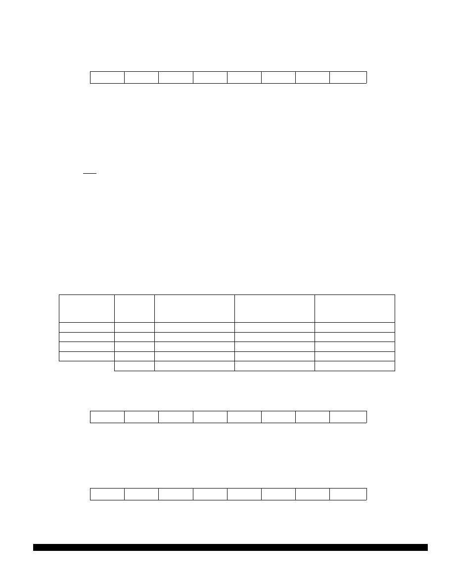
* Can be written only once in first 64 cycles out of reset in normal modes or at any time in special modes.
ADPU — A/D Power-Up
CSEL — Clock Select
5 Electrically Erasable Programmable Read-Only Memory (EE-
IRQE — IRQ Select Edge Sensitive Only
0 = Low level recognition
1 = Falling edge recognition
DLY — Enable Oscillator Start-Up Delay on Exit from STOP
0 = No stabilization delay on exit from STOP
1 = Stabilization delay enabled on exit from STOP
CME — Clock Monitor Enable
0 = Clock monitor disabled; slow clocks can be used
1 = Slow or stopped clocks cause clock failure reset
CR1, CR0 — COP Timer Rate Select
Write $55 to COPRST to arm COP watchdog clearing mechanism.
Write $AA to COPRST to reset COP watchdog.
RBOOT, SMOD, and MDA reset depends on conditions at reset and can only be written in special
modes (SMOD = 1).
OPTION
— System Configuration Options
$1039
Bit 7
6
5
4
3
2
1
Bit 0
ADPU
CSEL
IRQE*
DLY*
CME
0
CR1*
CR0*
RESET:
0
0
0
1
0
0
0
0
CR [1:0]
Divide
E/2
15
By
XTAL = 4.0 MHz
Time-Out
– 0/+32.8 ms
XTAL = 8.0 MHz
Time-Out
– 0/+16.4 ms
XTAL = 12.0 MHz
Time-Out
– 0/+10.9 ms
0
0
1
32.768 ms
16.384 ms
10.923 ms
0
1
4
131.072 ms
65.536 ms
43.691 ms
1
0
16
524.288 ms
262.140 ms
174.76 ms
1
1
64
2.097 sec
1.049 sec
699.05 ms
E =
1.0 MHz
2.0 MHz
3.0 MHz
COPRST
— Arm/Reset COP Timer Circuitry
$103A
Bit 7
6
5
4
3
2
1
Bit 0
7
6
5
4
3
2
1
0
RESET:
0
0
0
0
0
0
0
0
HPRIO
— Highest Priority I-Bit Interrupt and Miscellaneous
$103C
Bit 7
6
5
4
3
2
1
Bit 0
RBOOT
SMOD
MDA
IRVNE
PSEL3
PSEL2
PSEL1
PSEL0
RESET:
— — — —
0
1
0
1

MC68HC11L6
MOTOROLA
BR774/D
15
RBOOT
—
Read Bootstrap ROM
0 = Bootloader ROM disabled and not in map
1 = Bootloader ROM enabled and in map at $BF40–$BFFF
SMOD, MDA — Special Mode Select, Mode Select A
(Refer to
3 Operating Modes and Memory Maps
IRVNE — Internal Read Visibility/Not E
(Refer to
3 Operating Modes and Memory Maps
PSEL[3:0] — Priority Select Bit 3 through Bit 0
Writable only while the I bit in the CCR is set (interrupts disabled). These bits select one interrupt source
to be elevated above all other I-bit related sources.
PSEL [3:0)
Interrupt Source Promoted
0
0
0
0
Timer Overflow
0
0
0
1
Pulse Accumulator Overflow
0
0
1
0
Pulse Accumulator Input Edge
0
0
1
1
SPI Serial Transfer Complete
0
1
0
0
SCI Serial System
0
1
0
1
Reserved (Default to IRQ)
0
1
1
0
IRQ
0
1
1
1
Real-Time Interrupt
1
0
0
0
Timer Input Capture 1
1
0
0
1
Timer Input Capture 2
1
0
1
0
Timer Input Capture 3
1
0
1
1
Timer Output Compare 1
1
1
0
0
Timer Output Compare 2
1
1
0
1
Timer Output Compare 3
1
1
1
0
Timer Output Compare 4
1
1
1
1
Timer Output Compare 5/Input Capture 4

MOTOROLA
MC68HC11L6
16
BR774/D
5 Electrically Erasable Programmable Read-Only Memory (EEPROM)
The 512 bytes of EEPROM in the MC68HC11L6 are located at $B600 through $B7FF. The EEON bit
in CONFIG determines whether or not the EEPROM is in the memory map. When EEON = 1 (erased
state), the EEPROM is enabled; when EEON = 0, the EEPROM is disabled and out of the memory map.
EEON is reset to the value last programmed into CONFIG.
An on-chip charge pump develops the high voltage required for programming and erasing. When the
frequency of the E clock is less than 1 MHz, select an internal clock to drive the EEPROM charge pump
by writing one to the CSEL bit in the OPTION register.
Programming and erasing the EEPROM is controlled by the PPROG register and dependent upon the
block protect (BPROT) register value.
To erase the EEPROM, ensure that the proper bits of the BPROT register are cleared, then complete
the following steps using the PPROG register:
1.
Write to PPROG with the ERASE, EELAT, and appropriate BYTE and ROW bits set.
2.
Write to the appropriate EEPROM address with any data. Row erase only requires a write to
any location in the row. Bulk erase is accomplished by writing to any location in the array.
3.
Write to PPROG with ERASE, EELAT, EEPGM, and appropriate BYTE and ROW bits set.
4.
Delay for 10 ms or more, as appropriate.
5.
Clear the EEPGM bit in PPROG to turn off the high voltage.
6.
Clear the PPROG register to reconfigure the EEPROM address and data buses for normal op-
eration.
To program the EEPROM, ensure the proper bits of the BPROT register are cleared, then complete the
following steps with the PPROG register:
1.
Write to PPROG with the EELAT bit set.
2.
Write data to the desired address.
3.
Write to PPROG with the EELAT and EEPGM bits set.
4.
Delay for 10 ms or more, as appropriate.
5.
Clear the EEPGM bit in PPROG to turn off the high voltage.
6.
Clear the PPROG register to reconfigure the EEPROM address and data buses for normal op-
eration.
NOTE
Block protect register bits can be written to zero (protection disabled) within 64 cy-
cles of a reset in normal modes, or any time in special modes. Block protect regis-
ter bits can be written to one (protection enabled) at any time.
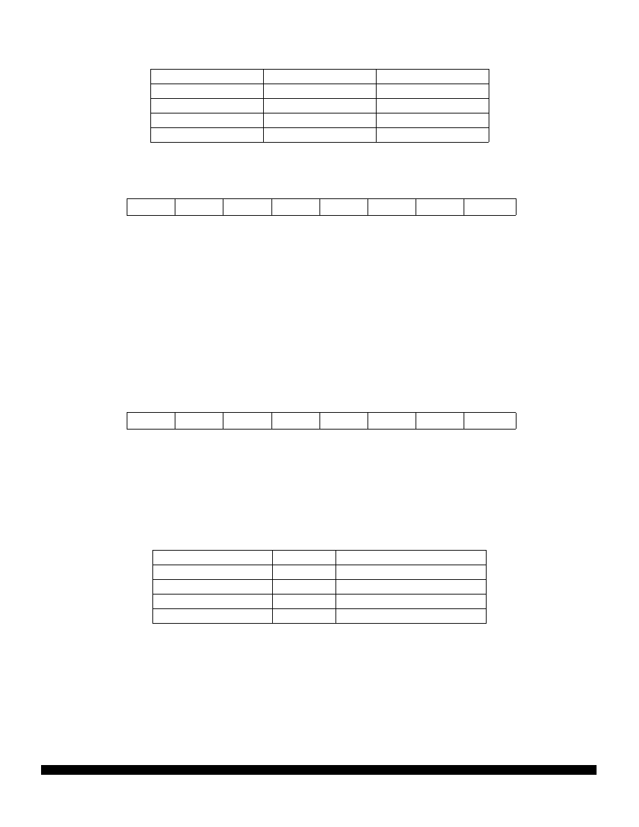
PTCON — Protect for CONFIG
0 = CONFIG register can be programmed or erased normally
1 = CONFIG register can not be programmed or erased
BPRT3–BPRT0 — Block Protect Bits for EEPROM
0 = Protection disabled for associated block
1 = Protection enabled for associated block
BPROT
— Block Protect
$1035
Bit 7
6
5
4
3
2
1
Bit 0
0
0
0
PTCON
BPRT3
BPRT2
BPRT1
BPRT0
RESET:
0
0
0
1
1
1
1
1
MC68HC11L6
MOTOROLA
BR774/D
17
*Can be written only once in first 64 cycles out of reset in normal modes or at any time in special modes.
ADPU — A/D Power-Up
(Refer to
CSEL — Clock Select
0 = A/D and EEPROM use system E clock
1 = A/D and EEPROM use internal RC clock
IRQE, DLY, CME, CR1, and CR0 —
(Refer to
ODD — Program Odd Rows in Half of EEPROM (TEST)
EVEN — Program Even Rows in Half of EEPROM (TEST)
BYTE — Byte/Other EEPROM Erase Mode
ROW — Row/All EEPROM Erase Mode
ERASE — Erase/Normal Control for EEPROM
0 = Normal read or program mode
1 = Erase mode
EELAT — EEPROM Latch Control
0 = EEPROM address and data bus configured for normal reads
1 = EEPROM address and data bus configured for programming or erasing
Bit Name
Block Protected
Block Size
BPRT0
$B600–$B61F
32 Bytes
BPRT1
$B620–$B65F
64 Bytes
BPRT2
$B660–$B6DF
128 Bytes
BPRT3
$B6E0–$B7FF
288 Bytes
OPTION
— System Configuration Options
$1039
Bit 7
6
5
4
3
2
1
Bit 0
ADPU
CSEL
IRQE*
DLY*
CME
0
CR1*
CR0*
RESET:
0
0
0
1
0
0
0
0
PPROG
— EEPROM Programming Control
$103B
Bit 7
6
5
4
3
2
1
Bit 0
ODD
EVEN
0
BYTE
ROW
ERASE
EELAT
EEPGM
RESET:
0
0
0
0
0
0
0
0
BYTE
ROW
Action
0
0
Bulk Erase (All 512 Bytes)
0
1
Row Erase (16 Bytes)
1
0
Byte Erase
1
1
Byte Erase

MOTOROLA
MC68HC11L6
18
BR774/D
EEPGM — EEPROM Program Command
0 = Programming or erase voltage to EEPROM array switched off
1 = Programming or erase voltage to EEPROM array switched on
NOSEC
— EEPROM Security Disable
NOSEC has no meaning unless the security mask option was specified at time of manufacture.
0 = Security enabled
1 = Security disabled
NOCOP — COP System Disable
0 = COP enabled (forces reset on time-out)
1 = COP disabled (does not force reset on time-out)
ROMON — ROM Enable
In single chip mode ROMON is forced to one out of reset.
0 = 16K ROM removed from the memory map
1 = 16K ROM present in the memory map
EEON
— EEPROM Enable
0 = EEPROM removed from the memory map
1 = EEPROM present in the memory map
CONFIG — EEPROM, ROM, COP Enables
$103F
Bit 7
6
5
4
3
2
1
Bit 0
0
0
0
0
NOSEC
NOCOP
ROMON
EEON
RESET:
0
0
0
0
—
—
—
—

MC68HC11L6
MOTOROLA
BR774/D
19
6 Parallel Input/Output
The MC68HC11L6 has up to 46 input/output lines, depending on the operating mode. Port A has three
input-only pins, three output-only pins, and two bidirectional I/O pins. Port A shares functions with the
timer system.
Port B is an eight-bit output-only port in single chip modes and is the high-order address in expanded
modes.
Port C is an eight-bit bidirectional port in single chip modes and the multiplexed address and data bus
in expanded modes.
Port D is an six-bit bidirectional port that shares functions with the serial systems.
Port E is an eight-bit input-only port that shares functions with the A/D Converter system.
Port G is an eight-bit bidirectional port in all modes.
6.1 Parallel I/O Handshake
Simple and full handshake input and output functions are available on ports B and C in single-chip
modes. The following is a description of the handshake functions.
In simple strobed mode, port B is a strobed output port and port C is a latching input port. The two ac-
tivities are available simultaneously.
The STRB output is pulsed for two E clock periods each time there is a write to the PORTB register.
The INVB bit in the PIOC register controls the polarity of STRB pulses. Port C levels are latched into
the alternate port C latch (PORTCL) register on each assertion of the STRA input. STRA edge select,
flag and interrupt enable bits are located in the PIOC register. Any or all of the port C lines may still be
used as general purpose I/O while in strobed input mode.
Full handshake modes involve port C pins and the STRA and STRB lines. Input and output handshake
modes are supported, and output handshake mode has a three-stated variation. STRA is an edge de-
tecting input, and STRB is a handshake output. Control and enable bits are located in the PIOC register.
In full input handshake mode, the MCU uses STRB as a “ready” line to an external system. Port C logic
levels are latched into PORTCL when the STRA line is asserted by the external system. The MCU then
negates STRB. The MCU reasserts STRB after the PORTCL register is read. A mix of latched inputs,
static inputs, and static outputs is allowed on port C, differentiated by the data direction bits and use of
the PORTC and PORTCL registers.
In full output handshake mode, the MCU writes data to PORTCL, which in turn asserts the STRB output
to indicate that data is ready. The external system reads port C and asserts the STRA input to acknowl-
edge that data has been received.
In the three-state variation of output handshake mode, lines intended as three-state handshake outputs
are configured as inputs by clearing the corresponding DDRC bits. The MCU writes data to PORTCL
and asserts STRB. The external system responds by activating the STRA input, which forces the MCU
to drive the data in PORTCL out on all of the port C lines. The mode variation does not allow part of port
C to be used for static inputs while other port C pins are being used for handshake outputs. (Refer also
to PIOC register description.)
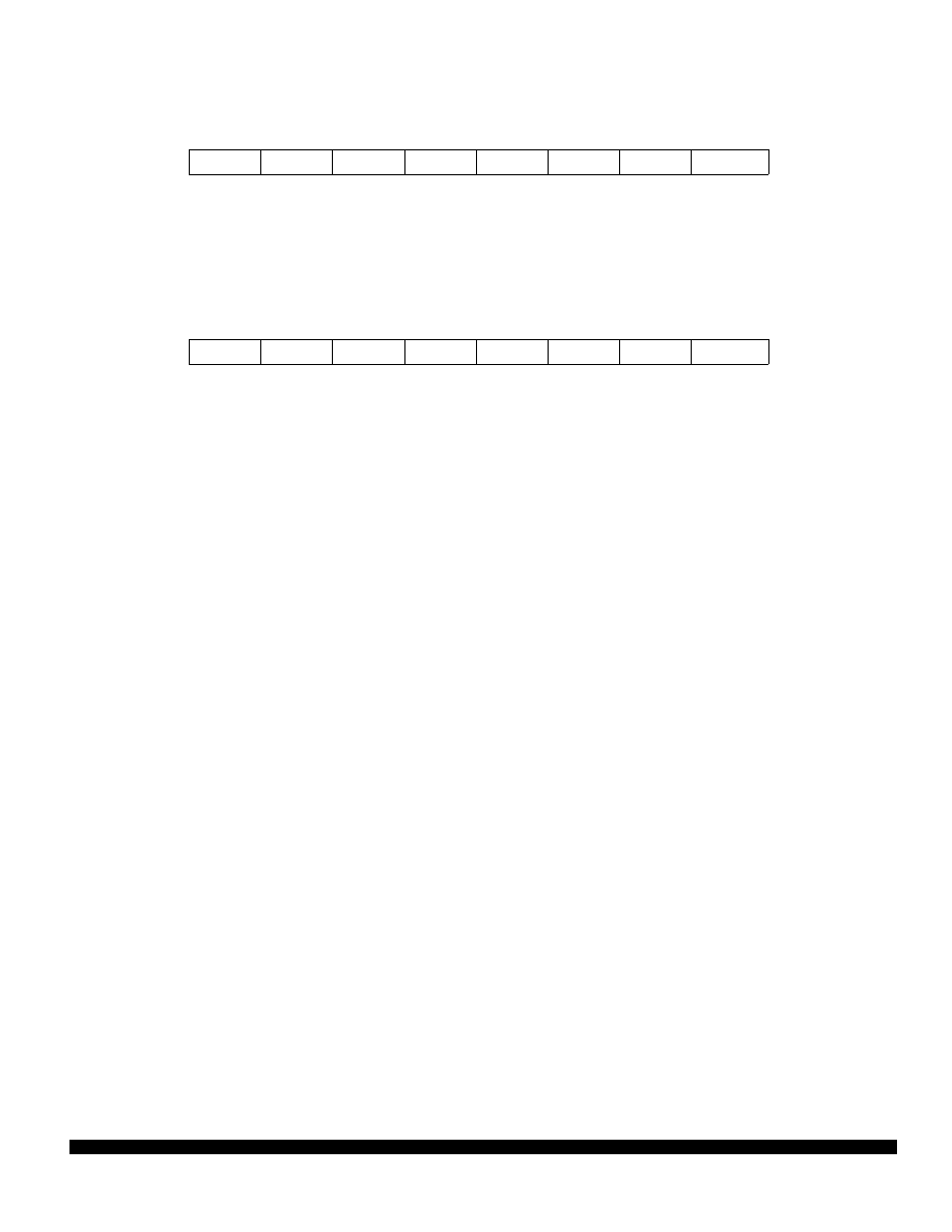
MOTOROLA
MC68HC11L6
20
BR774/D
STAF — Strobe A Interrupt Status Flag
Set when selected edge occurs on Strobe A. Cleared by PIOC read with STAF set followed by PORTCL
read (simple strobed or full input handshake mode) or PORTCL write (output handshake mode).
STAI — Strobe A Interrupt Enable Mask
0 = STAF interrupts disabled
1 = STAF interrupts enabled
CWOM — Port C Wire-OR Mode (affects all eight port C pins)
0 = Port C outputs are normal CMOS outputs
1 = Port C outputs are open-drain outputs
HNDS — Handshake Mode
0 = Simple strobe mode
1 = Full input or output handshake mode
OIN — Output or Input Handshake Select
HNDS must be set to one for this bit to have meaning.
0 = Input handshake
1 = Output handshake
PLS — Pulse/Interlocked Handshake Operation
HNDS must be set to one for this bit to have meaning.
0 = Interlocked handshake
1 = Pulsed handshake (Strobe B pulses high for two E- clock cycles.)
EGA — Active Edge for Strobe A
0 = STRA falling edge selected
1 = STRA rising edge selected
INVB — Invert Strobe B
0 = Active level is logic zero
1 = Active level is logic one
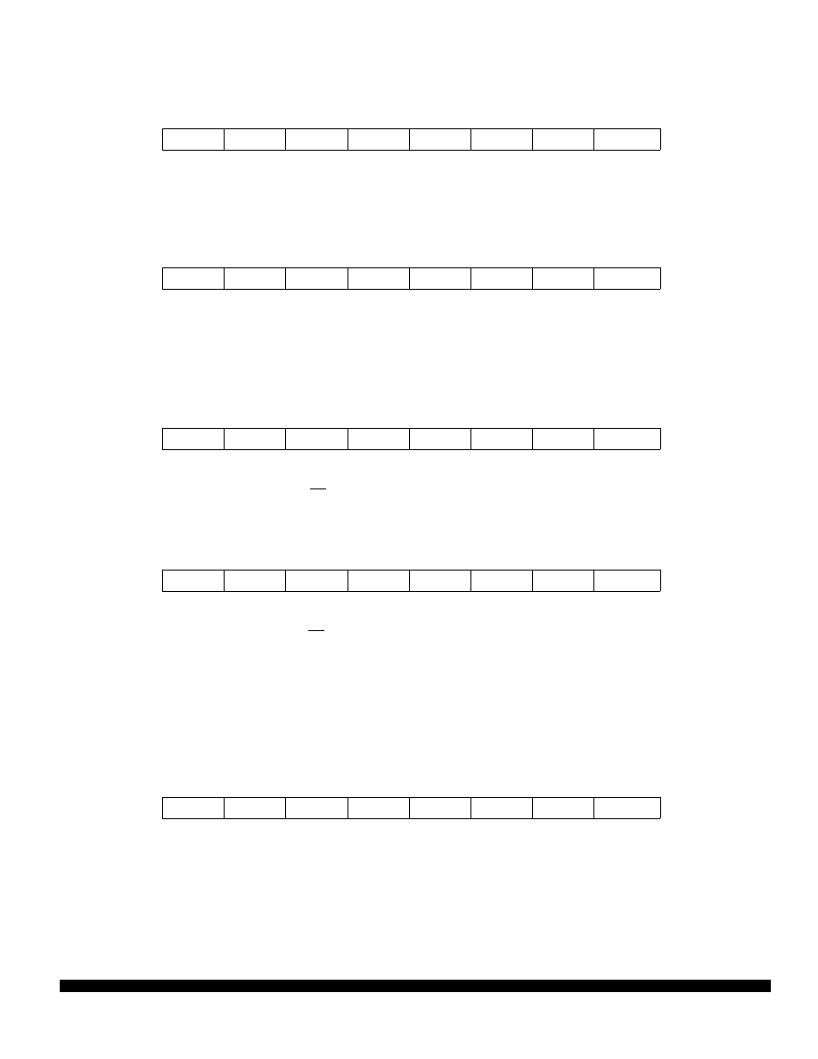
PORTA — Port A Data
$1000
Bit 7
6
5
4
3
2
1
Bit 0
PA7
PA6
PA5
PA4
PA3
PA2
PA1
PA0
RESET:
HiZ
0
0
0
HiZ
HiZ
HiZ
HiZ
Alt. Pin
Func.:
PAI
OC2
OC3
OC4
OC5/IC4
IC1
IC2
IC3
And/or:
OC1
OC1
OC1
OC1
OC1
—
—
—
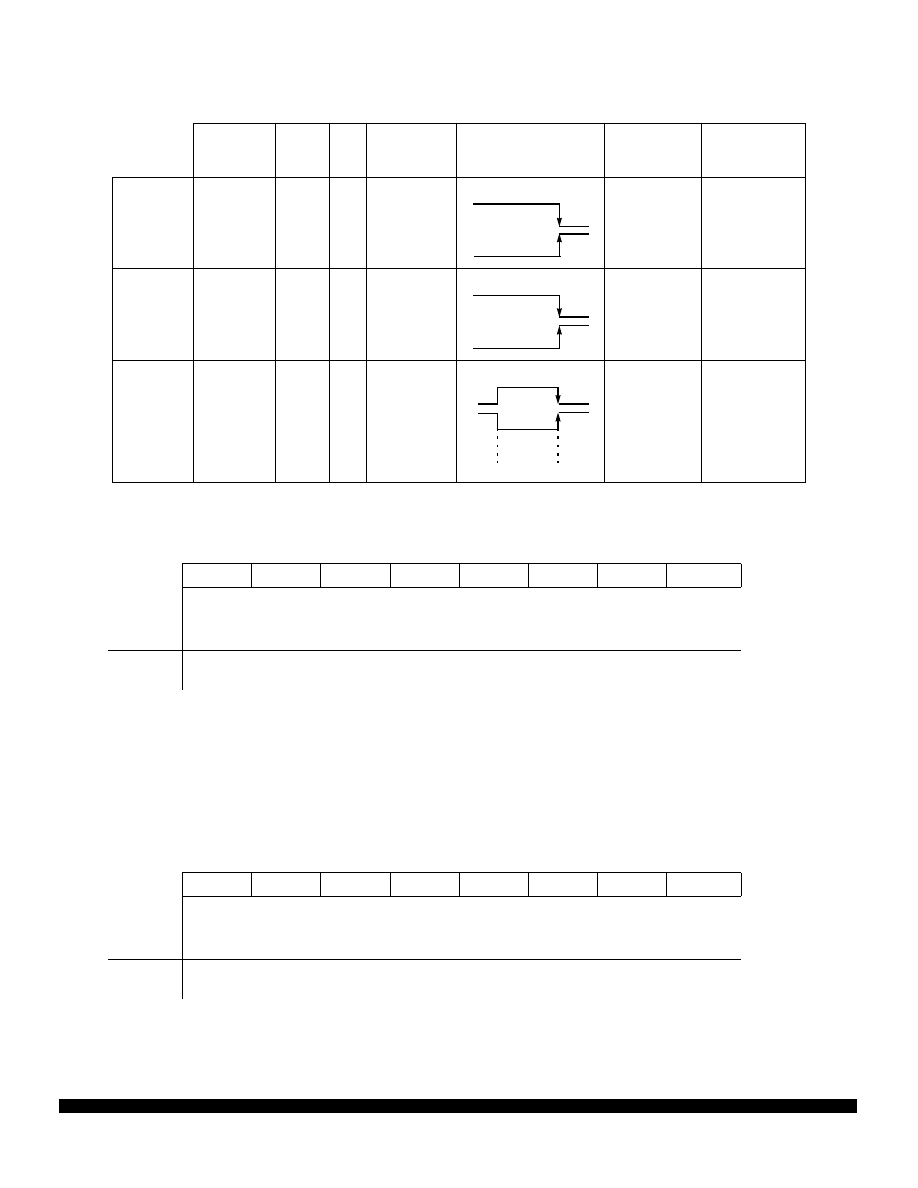
PIOC — Parallel I/O Control
$1002
Bit 7
6
5
4
3
2
1
Bit 0
STAF
STAI
CWOM
HNDS
OIN
PLS
EGA
INVB
RESET:
0
0
0
0
0
U
1
1
MC68HC11L6
MOTOROLA
BR774/D
21
NOTE
In single chip and boot modes, port C pins reset to high impedance inputs (DDRC
registers are set to zero). In expanded and special test modes, port C pins become
multiplexed address/data bus pins and the port C register address is treated as an
external memory location.
Table 4 Parallel I/O Control
STAF
Clearing
Sequence
HNDS
OIN
PLS
EGA
Port C
Port B
Simple
strobed
mode
Read PIOC
with STAF
=1 then read
PORTCL
0
X
X
Inputs latched
into PORTCL
on any active
edge on STRA
STRB pulses on
writes to port B
Full input
handshake
Read PIOC
with STAF
=1 then read
PORTCL
1
0
0 = STRB
active level
1 = STRB
active pulse
Inputs latched
into PORTCL
on any active
edge on STRA
Normal output
port, unaffected
in hand-shake
modes
Full output
handshake
Read PIOC
with STAF
=1 then
write to
PORTCL
1
1
0 = STRB
active level
1 = STRB
active pulse
Driven as out-
puts if STRA at
active level,
follows DDRC
if STRA not at
active level
Normal output
port, unaffected
in hand-shake
modes
PORTC — Port C Data
$1003
Bit 7
6
5
4
3
2
1
Bit 0
PC7
PC6
PC5
PC4
PC3
PC2
PC1
PC0
S. Chip
or Boot:
PC7
PC6
PC5
PC4
PC3
PC2
PC1
PC0
RESET:
0
0
0
0
0
0
0
0
Expan.
or Test:
ADDR7/
DATA7
ADDR6/
DATA6
ADDR5/
DATA5
ADDR4/
DATA4
ADDR3/
DATA3
ADDR2/
DATA2
ADDR1/
DATA1
ADDR0/
DATA0
PORTB — Port B Data
$1004
Bit 7
6
5
4
3
2
1
Bit 0
PB7
PB6
PB5
PB4
PB3
PB2
PB1
PB0
S. Chip or
Boot:
PB7
PB6
PB5
PB4
PB3
PB2
PB1
PB0
RESET:
0
0
0
0
0
0
0
0
Expan. or
Test:
ADDR15
ADDR14
ADDR13
ADDR12
ADDR11
ADDR10
ADDR9
ADDR8
1
0
0
1
0
1
Port C
Driven
STRA
Active Edge
Follow
DDRC
Follow
DDRC
MOTOROLA
MC68HC11L6
22
BR774/D
Writes affect port C pins. PORTCL is used in the handshake clearing mechanism.
When an active edge occurs on the STRA pin, port C data is latched into the PORTCL register.
DDC7–DDC0 — Data Direction for Port C
0 = Input
1 = Output
DDD5–DDD0 — Data Direction for Port D
When DDRD bit 5 is zero and MSTR = 1 in SPCR, PD5/SS is a general-purpose output, and mode fault
logic is disabled.
0 = Input
1 = Output
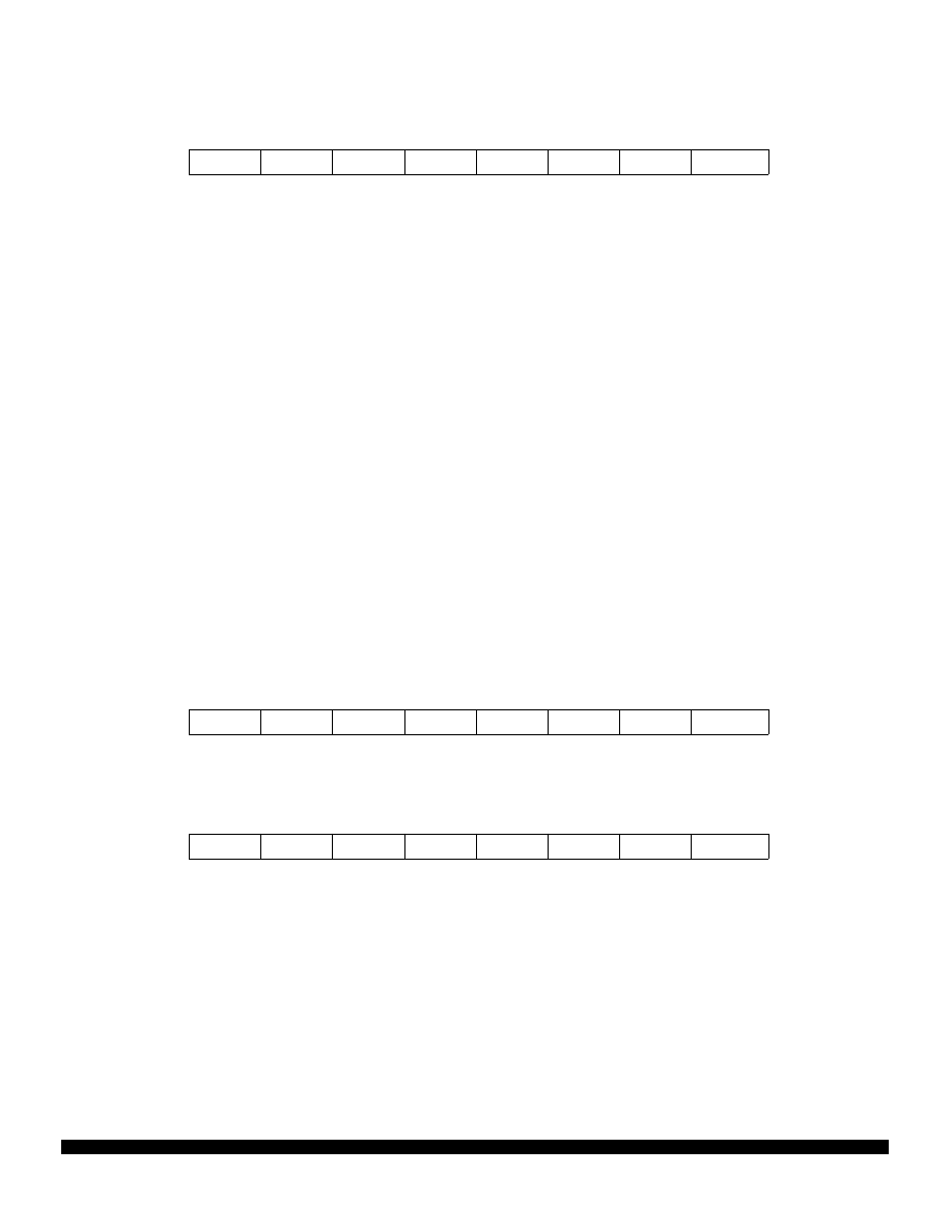
PORTCL — Port C Latched
$1005
Bit 7
6
5
4
3
2
1
Bit 0
PCL7
PCL6
PCL5
PCL4
PCL3
PCL2
PCL1
PCL0
RESET:
U
U
U
U
U
U
U
U
DDRC — Data Direction for Port C
$1007
Bit 7
6
5
4
3
2
1
Bit 0
DDC7
DDC6
DDC5
DDC4
DDC3
DDC2
DDC1
DDC0
RESET:
0
0
0
0
0
0
0
0
PORTD — Port D Data
$1008
Bit 7
6
5
4
3
2
1
Bit 0
0
0
PD5
PD4
PD3
PD2
PD1
PD0
RESET:
0
0
0
0
0
0
0
0
Alt. Pin
Func.:
—
—
SS SCK
MOSI
MISO
TxD
RxD
DDRD
— Data Direction for Port D
$1009
Bit 7
6
5
4
3
2
1
Bit 0
0
0
DDD5
DDD4
DDD3
DDD2
DDD1
DDD0
RESET:
0
0
0
0
0
0
0
0
Alt. Pin
Func.:
—
—
SS
SCK
MOSI
MISO
TxD
RxD
PORTE — Port E Data
$100A
Bit 7
6
5
4
3
2
1
Bit 0
PE7
PE6
PE5
PE4
PE3
PE2
PE1
PE0
RESET:
U
U
U
U
U
U
U
U
Alt. Pin
Func.:
AN7
AN6
AN5
AN4
AN3
AN2
AN1
AN0
MC68HC11L6
MOTOROLA
BR774/D
23
DDRA7 — Data Direction for Port A Bit 7
0 = Input
1 = Output
PAEN — Pulse Accumulator System Enable
(Refer to 10 Pulse Accumulator.)
PAMOD — Pulse Accumulator Mode
(Refer to 10 Pulse Accumulator.)
PEDGE — Pulse Accumulator Edge Control
(Refer to 10 Pulse Accumulator.)
DDRA3 — Data Direction for Port A Bit 3
Overridden if an output compare function is configured to control the PA3 pin.
0 = Input
1 = Output
I4/O5 — Input Capture Four/Output Compare 5
0 = OC5 enabled
1 = IC4 enabled
RTR1 and RT0 — Real-Time Interrupt (RTI) Rate
(Refer to 9 Main Timer.)
DDG7–DDG0 — Data Direction for Port G
0 = Input
1 = Output
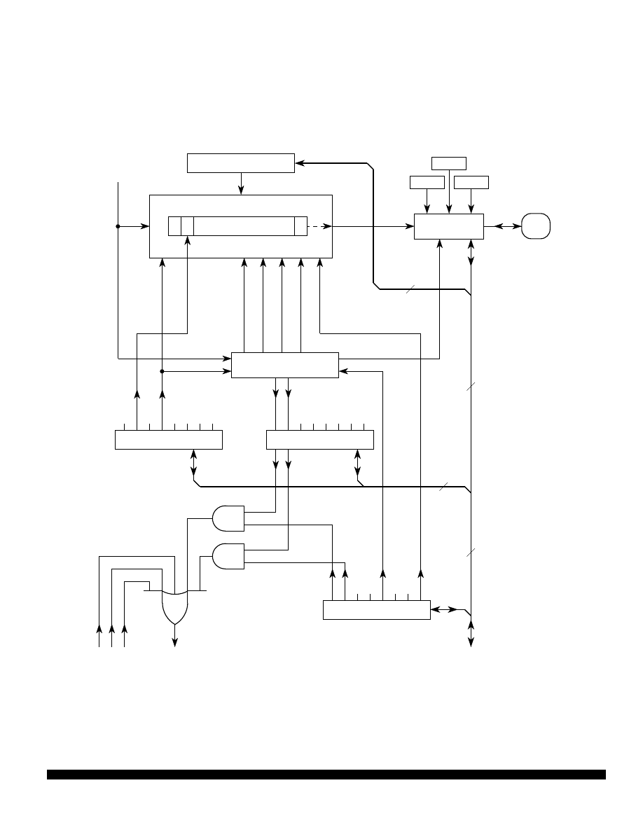
PACTL — Pulse Accumulator Control
$1026
Bit 7
6
5
4
3
2
1
Bit 0
DDRA7
PAEN
PAMOD
PEDGE
DDRA3
I4/O5
RTR1
RTR0
RESET:
0
0
0
0
0
0
0
0
PORTG — Port G Data
$1036
Bit 7
6
5
4
3
2
1
Bit 0
PG7
PG6
PG5
PG4
PG3
PG2
PG1
PG0
RESET:
0
0
0
0
0
0
0
0
DDRG — Data Direction for Port G
$1037
Bit 7
6
5
4
3
2
1
Bit 0
DDG7
DDG6
DDG5
DDG4
DDG3
DDG2
DDG1
DDG0
RESET:
0
0
0
0
0
0
0
0
MOTOROLA
MC68HC11L6
24
BR774/D
7 Serial Communications Interface (SCI)
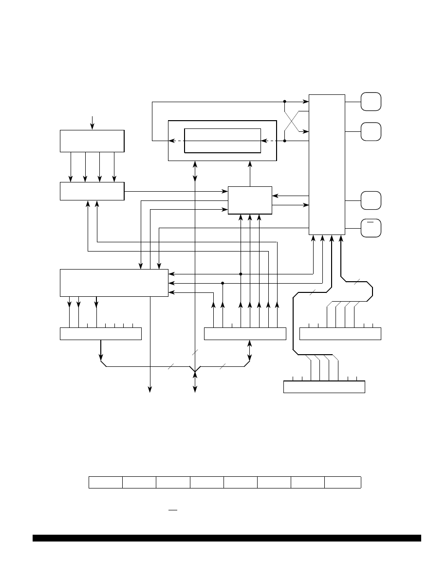
The SCI is a universal asynchronous receiver transmitter (UART) serial communications interface, one
of two independent serial I/O subsystems in the MC68HC11L6. It has a standard NRZ format (one start,
eight or nine data, and one stop bit) and several of baud rates available. The SCI transmitter and re-
ceiver are independent but use the same data format and bit rate.
Figure 6 SCI Transmitter Block Diagram
FE
NF
OR
IDLE
RDRF
TC
TDRE
SCSR INTERRUPT STATUS
SBK
RWU
RE
TE
ILIE
RIE
TCIE
TIE
SCCR2 SCI CONTROL 2
TRANSMITTER
CONTROL LOGIC
TCIE
TC
TIE
TDRE
SCI Rx
REQUESTS
SCI INTERRUPT
REQUEST
INTERNAL
DATA BUS
PIN BUFFER
AND CONTROL
H (8) 7
6
5
4
3
2
1
0
L
10 (11) - BIT Tx SHIFT REGISTER
DIO0
PD1/
TxD
SCDR Tx BUFFER
TRANSFER Tx BUFFER
SHIFT ENABLE
JAM ENABLE
PREAMBLE—JAM 1's
BREAK—JAM 0's
(WRITE-ONLY)
FORCE PIN
DIRECTION (OUT)
SIZE 8/9
WAKE
M
T8
R8
SCCR1 SCI CONTROL 1
TRANSMITTER
BAUD RATE
CLOCK
DDD1
DOD1
8
8
8
8
MC68HC11L6
MOTOROLA
BR774/D
25
Figure 7 SCI Receiver Block Diagram
FE
NF
OR
IDLE
RDRF
TC
TDRE
SCSR1 SCI STATUS 1
SBK
RWU
RE
TE
ILIE
RIE
TCIE
TIE
SCCR2 SCI CONTROL 2
WAKE
M
T8
R8
WAKE-UP
LOGIC
RIE
OR
ILIE
IDLE
SCI Tx
REQUESTS
SCI INTERRUPT
REQUEST
INTERNAL
DATA BUS
PD0/
RxD
SCDR Rx BUFFER
STOP
(8) 7
6
5
4
3
2
1
0
10 (11) - BIT
Rx SHIFT REGISTER
(READ-ONLY)
SCCR1 SCI CONTROL 1
RIE
RDRF
START
MSB
ALL ONES
DATA
RECOVERY
÷
16
RWU
RE
M
DISABLE
DRIVER
RECEIVER
BAUD RATE
CLOCK
8
8
8
PIN BUFFER
AND CONTROL
DIO0
DDD0
DOD0
MOTOROLA
MC68HC11L6
26
BR774/D
DWOM — Port D Wired-OR Mode (affects all six port D pins)
0 = Normal CMOS outputs
1 = Open-drain outputs
Refer to SPI section for all other bits.
TCLR — Clear Baud Rate Counters (TEST)
RCKB — SCI Baud Rate Clock Check (TEST)
SCP1, SCP0 — SCI Baud Rate Prescaler Selects
SCR2, SCR1, and SCR0 — SCI Baud Rate Selects
Selects receiver and transmitter bit rate based on output from baud rate prescaler stage
SPCR — Serial Peripheral Control
$1028
Bit 7
6
5
4
3
2
1
Bit 0
SPIE
SPE
DWOM
MSTR
CPOL
CPHA
SPR1
SPR0
RESET:
0
0
0
0
0
1
U
U
BAUD — Baud Rate
$102B
Bit 7
6
5
4
3
2
1
Bit 0
TCLR
0
SCP1
SCP0
RCKB
SCR2
SCR1
SCR0
RESET:
0
0
0
0
0
U
U
U
SCP [1:0]
Divide
Internal Clock
By
Crystal Frequency in MHz
1
0
4.0 MHz
(Baud)
8.0 MHz
(Baud)
10.0 MHz
(Baud)
12.0 MHz
(Baud)
0
0
1
62.50K
125.0K
156.25K
187.5K
0
1
3
20.83K
41.67K
52.08K
62.5K
1
0
4
15.625K
31.25K
38.4K
46.88K
1
1
13
4800
9600 12.02K
14.42K
SCR Bit [2:0]
Divide
Prescaler
By
Highest Baud Rate
(Prescaler Output from Previous Table)
4800
9600
38.4K
0
0
0
1
4800
9600
38.4K
0
0
1
2
2400
4800
19.2K
0
1
0
4
1200
2400
9600
0
1
1
8
600
1200
4800
1
0
0
16
300
600
2400
1
0
1
32
150
300
1200
1
1
0
64
—
150
600
1
1
1
128
—
—
300
MC68HC11L6
MOTOROLA
BR774/D
27
Figure 8 SCI Baud Rate
R8 — Receive Data Bit 8
If M bit is set, R8 stores ninth bit in receive data character.
T8 — Transmit Data bit 8
If M bit is set, T8 stores ninth bit in transmit data character.
M — Mode (Select Character Format)
0 = Start, 8 data bits, 1 stop bit
1 = Start, 9 data bits, 1 stop bit
SCCR1 — SCI Control 1
$102C
Bit 7
6
5
4
3
2
1
Bit 0
R8
T8
0
M
WAKE
0
0
0
RESET:
U
U
0
0
0
0
0
0
OSCILLATOR
AND
CLOCK GENERATOR
(
÷
4)
XTAL
EXTAL
E
AS
SCP1:SCP0
SCI
RECEIVE
BAUD RATE
(16X)
SCI
TRANSMIT
BAUD RATE
(1X)
SCR2:SCR1:SCR0
÷
2
÷
2
÷
2
÷
2
÷
2
÷
2
0:0:1
0:1:0
0:1:1
1:0:0
1:0:1
1:1:0
1:1:1
0:0:0
÷
2
÷
16
÷
3
÷
4
÷
13
0:0
0:1
1:0
1:1
INTERNAL
BUS
CLOCK
(PH2)
MOTOROLA
MC68HC11L6
28
BR774/D
WAKE — Wake-Up by Address Mark/Idle
0 = Wake up by IDLE line recognition
1 = Wake up by address mark (most significant data bit set)
TIE — Transmit Interrupt Enable
0 = TDRE interrupts disabled
1 = SCI interrupt requested when TDRE status flag is set
TCIE — Transmit Complete Interrupt Enable
0 = TC interrupts disabled
1 = SCI interrupt requested when TC status flag is set
RIE — Receiver Interrupt Enable
0 = RDRF and OR interrupts disabled
1 = SCI interrupt requested when RDRF flag or the OR status flag is set
ILIE — Idle Line Interrupt Enable
0 = IDLE interrupts disabled
1 = SCI interrupt requested when IDLE status flag is set
TE — Transmitter Enable
When TE goes form zero to one, one unit of idle character time (logic one) is queued as a preamble.
0 = Transmitter disabled
1 = Transmitter enabled
RE — Receiver Enable
0 = Receiver disabled
1 = Receiver enabled
RWU — Receiver Wake-Up Control
0 = Normal SCI receiver
1 = Wake-up enabled and receiver interrupts inhibited
SBK — Send Break
0 = Break generator off
1 = Break codes generated as long as SBK = 1
TDRE — Transmit Data Register Empty Flag
Set if transmit data can be written to SCDR; if TDRE = 0, transmit data register is busy.
Cleared by SCSR read with TDRE set, followed by SCDR write.
TC — Transmit Complete Flag
Set if transmitter is idle (no data, preamble, or break transmission in progress).
Cleared by SCSR read with TC set, followed by SCDR write.
SCCR2 — SCI Control 2
$102D
Bit 7
6
5
4
3
2
1
Bit 0
TIE
TCIE
RIE
ILIE
TE
RE
RWU
SBK
RESET:
0
0
0
0
0
0
0
0
SCSR — SCI Status
$102E
Bit 7
6
5
4
3
2
1
Bit 0
TDRE
TC
RDRF
IDLE
OR
NF
FE
0
RESET:
1
1
0
0
0
0
0
0
MC68HC11L6
MOTOROLA
BR774/D
29
RDRF — Receive Data Register Full Flag
Set if a received character is ready to be read from SCDR.
Cleared by SCSR read with RDRF set, followed by SCDR read.
IDLE — Idle Line Detected Flag
Set if the RxD line is idle. IDLE flag is inhibited when RWU = 1.
Cleared by SCSR read with IDLE set, followed by SCDR read.
Once cleared, IDLE is not be set again until the RxD line has been active and becomes idle again.
OR — Overrun Error Flag
Set if a new character is received before a previously received character is read from SCDR.
Cleared by SCSR read with OR set, followed by SCDR read.
NF — Noise Error Flag
Set if majority sample logic detects anything other than a unanimous decision.
Cleared by SCSR read with NF set, followed by SCDR read.
FE — Framing Error
Set if a 0 is detected where a stop bit was expected.
Cleared by SCSR read with FE set, followed by SCDR read.
Receive and transmit are double buffered. Reads access the receive data buffer, and writes access the
transmit data buffer.
SCDR — SCI Data
$102F
Bit 7
6
5
4
3
2
1
Bit 0
R7/T7
R6/T6
R5/T5
R4/T4
R3/T3
R2/T2
R1/T1
R0/T0
RESET:
U
U
U
U
U
U
U
U
MOTOROLA
MC68HC11L6
30
BR774/D
8 Serial Peripheral Interface (SPI)
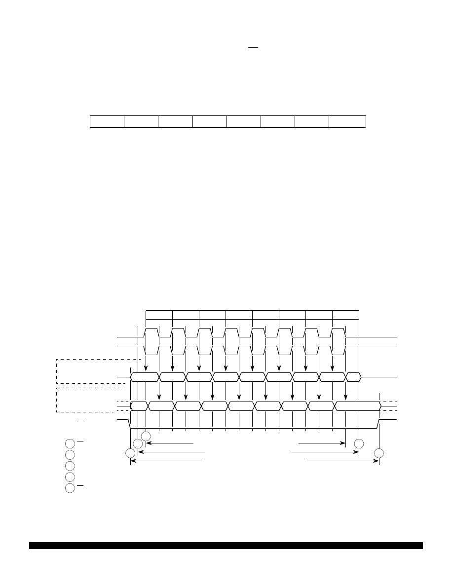
The SPI, an independent serial communications subsystem, allows the MCU to communicate synchro-
nously with peripheral devices and other microprocessors. Data rates can be as high as one-half of the
E-clock rate when configured as a master and as fast as the E clock when configured as a slave.
Figure 9 SPI Block Diagram
DDRD — Data Direction for Port D
$1009
Bit 7
6
5
4
3
2
1
Bit 0
0
0
DDD5
DDD4
DDD3
DDD2
DDD1
DDD0
RESET:
0
0
0
0
0
0
0
0
Alt. Pin
Func.:
—
—
SS
SCK
MOSI
MISO
TxD
RxD
INTERNAL
MCU CLOCK
DIVIDER
÷
2
÷
4
÷
16
÷
32
SELECT
SPI CLOCK (MASTER)
8-BIT SHIFT REGISTER
READ DATA BUFFER
CLOCK
CLOCK
LOGIC
S
M
M
S
PIN
CONTROL
LOGIC
MISO/
PD2
MOSI/
PD3
SCK/
PD4
SS/
PD5
M
S
MSTR
SPE
DIO[5:2]
SPR1
SPR0
MSTR
SPE
SPIE
SPIE
SPE
MSTR
CPHA
CPOL
SPR1
SPR0
SPCR SPI CONTROL REGISTER
SPIF
WCOL
MODF
SPSR SPI STATUS REGISTER
SPI CONTROL
INTERNAL
DATA BUS
SPI INTERRUPT
REQUEST
DOD[5:2]
DIO4
DIO3
DIO2
DIO1
DIO0
PORT D I/O CONTROL
DIO5
DOD4
DOD3
DOD2
DOD1
DOD0
PORT D OUTPUT MODE
DOD5
8
8
4
4
8
MSB
LSB
MC68HC11L6
MOTOROLA
BR774/D
31
DDD5–DDD0 — Data Direction for Port D
When DDRD bit 5 is zero and MSTR = 1 in SPCR, PD5/SS is a general-purpose output and mode fault
logic is disabled.
0 = Input
1 = Output
SPIE — Serial Peripheral Interrupt Enable
0 = SPI interrupts disabled
1 = SPI interrupts enabled
SPE — Serial Peripheral System Enable
0 = SPI off
1 = SPI on
DWOM — Port D Wired-OR Mode
DWOM affects all six port D pins
0 = Normal CMOS outputs
1 = Open-drain outputs
MSTR — Master Mode Select
0 = Slave mode
1 = Master mode
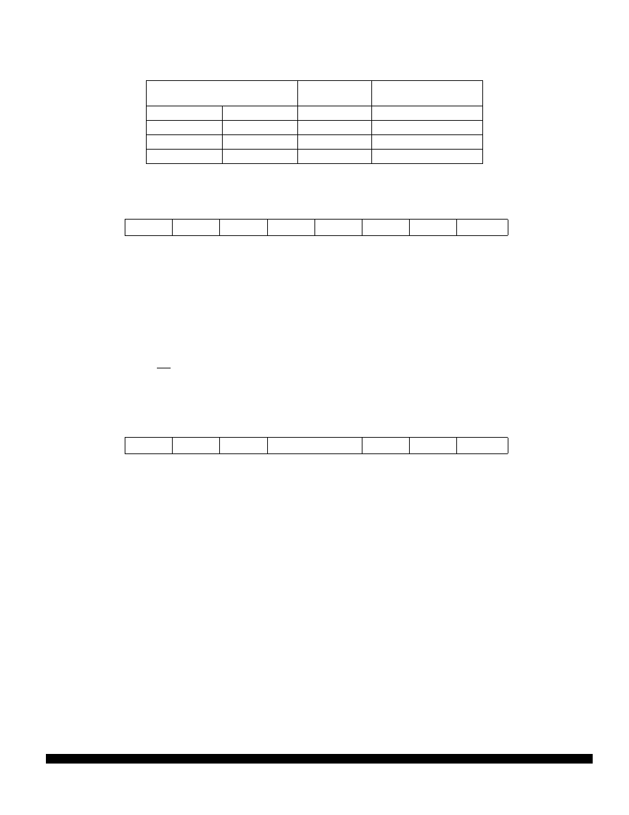
CPOL, CPHA — Clock Polarity, Clock Phase (Refer to Figure 10.)
Figure 10 SPI Transfer Format
SPCR — Serial Peripheral Control
$1028
Bit 7
6
5
4
3
2
1
Bit 0
SPIE
SPE
DWOM
MSTR
CPOL
CPHA
SPR1
SPR0
RESET:
0
0
0
0
0
1
U
U
2
3
4
5
6
7
8
1
SCK (CPOL = 1)
SCK (CPOL = 0)
SCK CYCLE #
SS (TO SLAVE)
6
5
4
3
2
1
LSB
MSB
MSB
6
5
4
3
2
1
LSB
SAMPLE INPUT
DATA OUT
SAMPLE INPUT
DATA OUT
(CPHA = 1)
(CPHA = 0)
SLAVE CPHA = 1 TRANSFER IN PROGRESS
MASTER TRANSFER IN PROGRESS
SLAVE CPHA = 0 TRANSFER IN PROGRESS
3
2
1
5
4
SS ASSERTED
MASTER WRITES
FIRST SCK EDGE
SPIF SET
SS NEGATED
1
2
3
4
5
TO SPDR
MOTOROLA
MC68HC11L6
32
BR774/D
SPR1 and SPR0 — SPI Clock Rate Selects
SPIF — SPI Transfer Complete Flag
Set when an SPI transfer is complete.
Cleared by reading SPSR with SPIF set, followed by SPDR access.
WCOL — Write Collision
Set when SPDR is written while transfer is in progress.
Cleared by SPSR with WCOL set, followed by SPDR access.
MODF — Mode Fault (A Mode Fault Terminates SPI Operation)
Set when SS is pulled low while MSTR = 1.
Cleared by SPSR read with MODF set, followed by SPCR write.
NOTE
SPI is double buffered in, single buffered out.
SPR [1:0]
E Clock
Divide By
Frequency at
E = 2 MHz (Baud)
0
0
2
1.0 MHz
0
1
4
500 kHz
1
0
16
125 kHz
1
1
32
62.5 kHz
SPSR — Serial Peripheral Status
$1029
Bit 7
6
5
4
3
2
1
Bit 0
SPIF
WCOL
0
MODF
0
0
0
0
RESET:
0
0
0
0
0
0
0
0
SPDR — SPI Data
$102A
Bit 7
6
5
4
3
2
1
Bit 0
Bit 7
6
5
4
3
2
1
Bit 0

MC68HC11L6
MOTOROLA
BR774/D
33
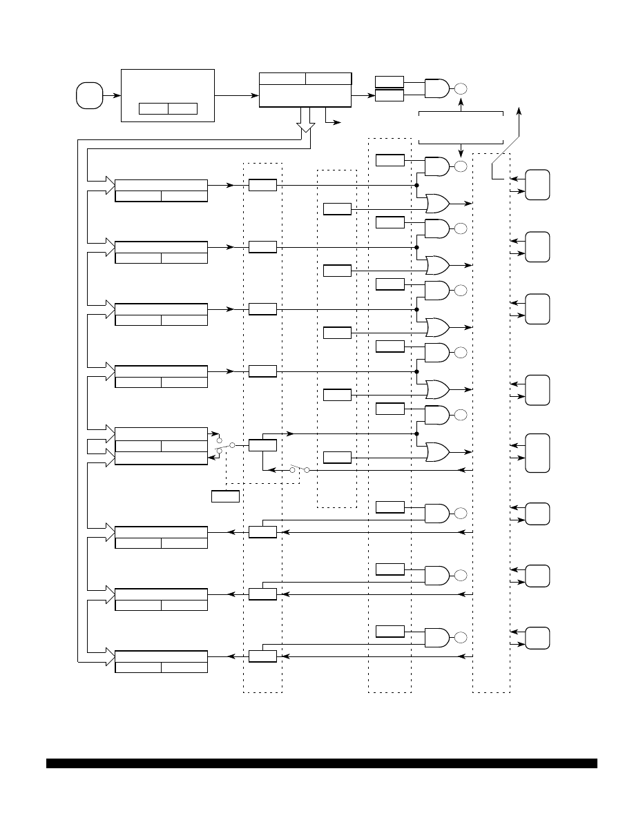
9 Main Timer
The main timer is based on a free-running 16-bit counter with a four-stage programmable prescaler. A
timer overflow function allows software to extend the system's timing capability beyond the counter's
16-bit range.
The timer has three channels of input capture, four channels of output compare, and one channel that
can be configured as a fourth input capture or a fifth output compare.
The following table summarizes crystal-related frequencies and periods.
Table 5 Timer Summary
XTAL Frequencies
4.0 MHz
8.0 MHz
12.0 MHz
Other Rates
Control
1.0 MHz
2.0 MHz
3.0 MHz
(E)
Bits
1000 ns
500 ns
333 ns
(1/E)
PR [1:0]
Main Timer Count Rates
0 0
1 count
overflow
1.0
µ
s
65.536 ms
500 ns
32.768 ms
333 ns
21.845 ms
(E/1)
(E/2
16
)
0 1
1 count
overflow
4.0
µ
s
262.14 ms
2.0
µ
s
131.07 ms
1.333
µ
s
87.381 ms
(E/4)
(E/2
18
)
1 0
1 count
overflow
8.0
µ
s
524.29 ms
4.0
µ
s
262.14 ms
2.667
µ
s
174.76 ms
(E/8)
(E/2
19
)
1 1
1 count
overflow
16.0
µ
s
1.049 s
8.0
µ
s
524.29 ms
5.333
µ
s
349.52 ms
(E/16)
(E/2
20
)
RTR [1:0]
Periodic (RTI) Interrupt Rates
0 0
0 1
1 0
1 1
8.192 ms
16.384 ms
32.768 ms
65.536 ms
4.096 ms
8.192 ms
16.384 ms
32.768 ms
2.731 ms
5.461 ms
10.923 ms
21.845 ms
(E/2
13
)
(E/2
14
)
(E/2
15
)
(E/2
16
)
CR [1:0]
COP Watchdog Time-Out Rates
0 0
0 1
1 0
1 1
32.768 ms
131.07 ms
524.29 ms
2.097 s
16.384 ms
65.536 ms
262.14 ms
1.049 s
10.923 ms
43.691 ms
174.76 ms
699.05 ms
(E/2
15
)
(E/2
17
)
(E/2
19
)
(E/2
21
)
Time-Out Tolerance
(– 0 ms/+...)
32.768 ms
16.4 ms
10.9 ms
(E/2
15
)
MOTOROLA
MC68HC11L6
34
BR774/D
Figure 11 Main Timer
PA3
OC5/
IC4/
OC1
16-BIT LATCH
CLK
TIC1 (HI)
16-BIT COMPARATOR =
IC3F
OC2F
OC3F
I4/O5F
TFLG1
TMSK1
IC1F
IC1I
3
IC2F
IC2I
2
IC3I
1
OC4F
I4/O5I
16-BIT TIMER BUS
16-BIT FREE-RUNNING
COUNTER
TCNT (HI)
TOF
TOI
9
PR1
PR0
PRESCALER–DIVIDE BY
1, 4, 8, OR 16
I4/O5
OC1I
8
FOC1
OC2I
7
FOC2
OC3I
6
FOC3
OC4I
5
FOC4
4
FOC5
STATUS
FLAGS
FORCE
OUTPUT
COMPARE
INTERRUPT
ENABLES
PORT A
OC5
IC4
CFORC
16-BIT TIMER BUS
OC1F
BIT 7
BIT 6
BIT 5
BIT 4
BIT 3
BIT 2
BIT 1
BIT 0
PIN
FUNCTIONS
TCNT (LO)
PA2/
IC1
TIC1 (LO)
16-BIT LATCH
CLK
TIC2 (HI)
TIC2 (LO)
16-BIT LATCH
CLK
TIC3 (HI)
TIC3 (LO)
TOC1 (HI)
TOC1 (LO)
TOC2 (HI)
TOC2 (LO)
TOC3 (HI)
TOC3 (LO)
TOC4 (HI)
TOC4 (LO)
16-BIT LATCH
CLK
TI4/O5 (HI)
TI4/O5 (LO)
16-BIT COMPARATOR =
16-BIT COMPARATOR =
16-BIT COMPARATOR =
16-BIT COMPARATOR =
MCU
ECLK
INTERRUPT REQUESTS
(FURTHER QUALIFIED
BY I BIT IN CCR)
PIN
CONTROL
PA7/
OC1/
PAI
PA6/
OC2/
OC1
PA5/
OC3/
OC1
PA4/
OC4/
OC1
PA1/
IC2
PA0/
IC3
TO
PULSE
ACCUMULATOR
TAPS FOR RTI, COP
WATCHDOG AND
PULSE ACCUMULATOR
MC68HC11L6
MOTOROLA
BR774/D
35
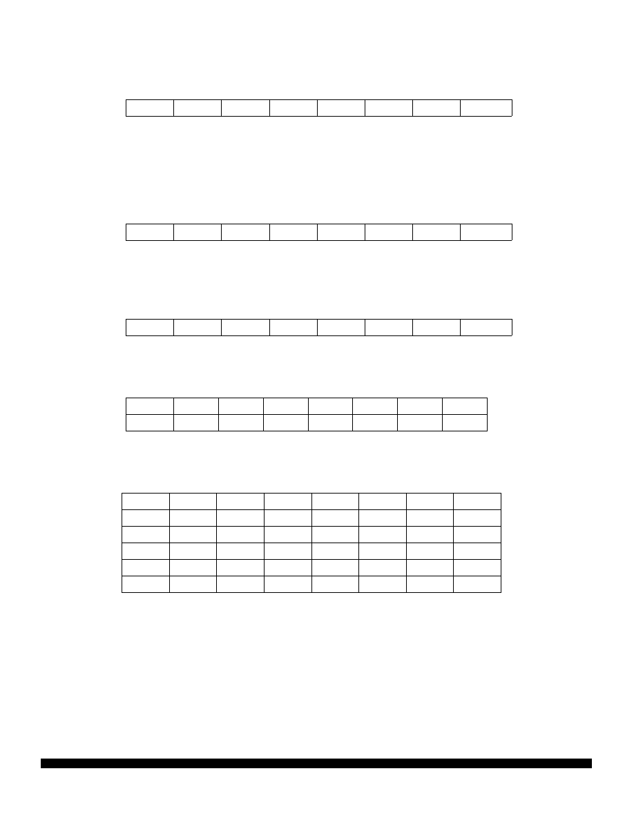
FOC5–FOC1 — Write ones to Force Compare(s)
0 = Not affected
1 = Output x action occurs
Set bit(s) to enable OC1 to control corresponding pin(s) of port A
If OC1Mx is set, data in OC1Dx is output to port A bit x on successful OC1 compares
TCNT resets to $0000.
In normal modes, TCNT is read-only.
TICx is not affected by reset.
CFORC — Timer Compare Force
$100B
Bit 7
6
5
4
3
2
1
Bit 0
FOC1
FOC2
FOC3
FOC4
FOC5
0
0
0
RESET:
0
0
0
0
0
0
0
0
OC1M — Output Compare 1 Mask
$100C
Bit 7
6
5
4
3
2
1
Bit 0
OC1M7
OC1M6
OC1M5
OC1M4
OC1M3
0
0
0
RESET:
0
0
0
0
0
0
0
0
OC1D — Output Compare 1 Data
$100D
Bit 7
6
5
4
3
2
1
Bit 0
OC1D7
OC1D6
OC1D5
OC1D4
OC1D3
0
0
0
RESET:
0
0
0
0
0
0
0
0
TCNT — Timer Counter
$100E, $100F
$100E
Bit 15
14
13
12
11
10
9
Bit 8
TCNT (High)
$100F
Bit 7
6
5
4
3
2
1
Bit 0
TCNT (Low)
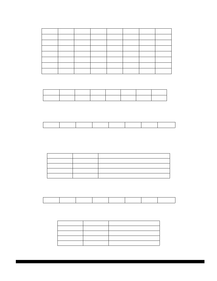
TIC1–TIC3 — Timer Input Capture
$1010–$1015
$1010
Bit 15
14
13
12
11
10
9
Bit 8
TIC1 (High)
$1011
Bit 7
6
5
4
3
2
1
Bit 0
TIC1 (Low)
$1012
Bit 15
14
13
12
11
10
9
Bit 8
TIC2 (High)
$1013
Bit 7
6
5
4
3
2
1
Bit 0
TIC2 (Low)
$1014
Bit 15
14
13
12
11
10
9
Bit 8
TIC3 (High)
$1015
Bit 7
6
5
4
3
2
1
Bit 0
TIC3 (Low)
MOTOROLA
MC68HC11L6
36
BR774/D
All TOCx register pairs reset to ones ($FFFF).
All TI4/O5 register pairs reset to ones ($FFFF).
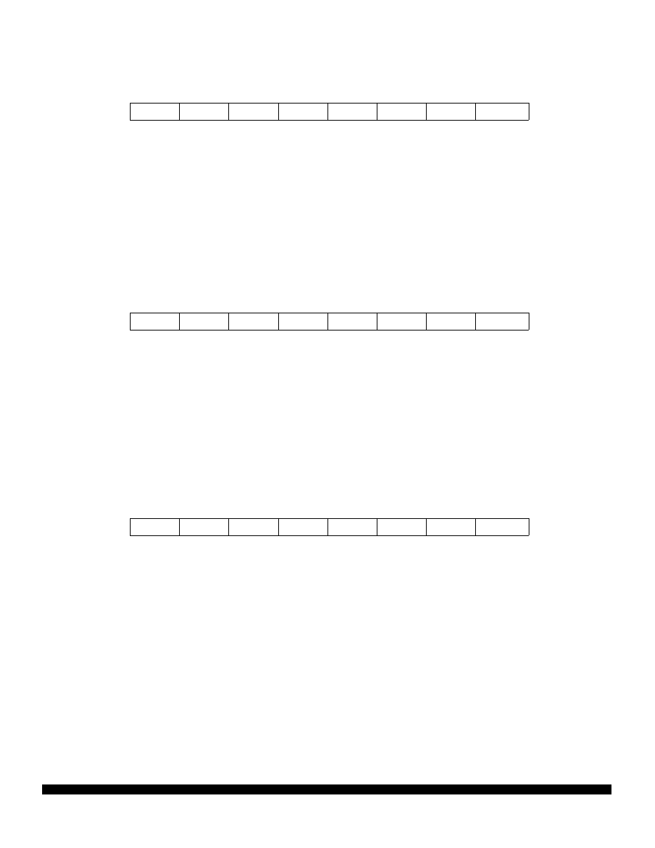
OM2–OM5 — Output Mode
OL2–OL5 — Output Level
TOC1–TOC4 — Timer Output Compare
$1016–$101D
$1016
Bit 15
14
13
12
11
10
9
Bit 8
TOC1 (High)
$1017
Bit 7
6
5
4
3
2
1
Bit 0
TOC1 (Low)
$1018
Bit 15
14
13
12
11
10
9
Bit 8
TOC2 (High)
$1019
Bit 7
6
5
4
3
2
1
Bit 0
TOC2 (Low)
$101A
Bit 15
14
13
12
11
10
9
Bit 8
TOC3 (High)
$101B
Bit 7
6
5
4
3
2
1
Bit 0
TOC3 (Low)
$101C
Bit 15
14
13
12
11
10
9
Bit 8
TOC4 (High)
$101D
Bit 7
6
5
4
3
2
1
Bit 0
TOC4 (Low)
TI4/O5 — Timer Input Capture 4/Output Compare 5
$101E, $101F
$101E
Bit 15
14
13
12
11
10
9
Bit 8
TI4/O5 (High)
$101F
Bit 7
6
5
4
3
2
1
Bit 0
TI4/O5 (Low)
TCTL1 — Timer Control 1
$1020
Bit 7
6
5
4
3
2
1
Bit 0
OM2
OL2
OM3
OL3
OM4
OL4
OM5
OL5
RESET:
0
0
0
0
0
0
0
0
OMx
OLx
Action Taken on Successful Compare
0
0
Timer disconnected from output pin logic.
0
1
Toggle OCx output line.
1
0
Clear OCx output line to zero.
1
1
Set OCx output line to one.
TCTL2 — Timer Control 2
$1021
Bit 7
6
5
4
3
2
1
Bit 0
EDG4B
EDG4A
EDG1B
EDG1A
EDG2B
EDG2A
EDG3B
EDG3A
RESET:
0
0
0
0
0
0
0
0
Table 6 Timer Control Configuration
EDGxB
EDGxA
Configuration
0
0
Capture disabled
0
1
Capture on rising edges only
1
0
Capture on falling edges only
1
1
Capture on any edge
MC68HC11L6
MOTOROLA
BR774/D
37
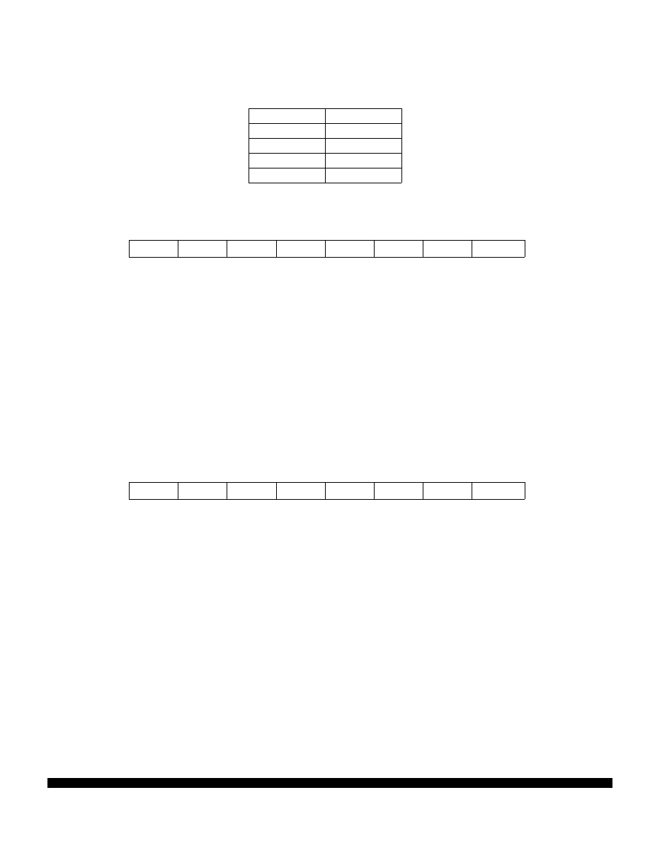
OC1I–OC4I — Output Compare x Interrupt Enable
I4/O5I — Input Capture 4 or Output Compare 5 Interrupt Enable
IC1I–IC3I — Input Capture x Interrupt Enable
NOTE
Bits in TMSK1 correspond bit for bit with flag bits in TFLG1. Ones in TMSK1 enable
the corresponding interrupt sources.
Clear flags by writing a one to the corresponding bit position(s).
OC1F–OC4F — Output Compare x Flag
Set each time the counter matches output compare x value
I4/O5F — Input Capture 4/Output Compare 5 Flag
Set by IC4 or OC5, depending on which function was enabled by I4/O5 in PACTL
IC1F–IC3F — Input Capture x Flag
Set each time a selected active edge is detected on the ICx input line
TOI — Timer Overflow Interrupt Enable
RTII — Real-time Interrupt Enable
PAOVI — Pulse Accumulator Overflow Interrupt Enable
(Refer to Pulse Accumulator.)
PAII — Pulse Accumulator Input Edge Interrupt Enable
(Refer to Pulse Accumulator.)
NOTE
Bits in TMSK2 correspond bit for bit with flag bits in TFLG2. Ones in TMSK2 enable
the corresponding interrupt sources.
TMSK1 — Timer Interrupt Mask 1
$1022
Bit 7
6
5
4
3
2
1
Bit 0
OC1I
OC2I
OC3I
OC4I
I4/O5I
IC1I
IC2I
IC3I
RESET:
0
0
0
0
0
0
0
0
TFLG1 — Timer Interrupt Flag 1
$1023
Bit 7
6
5
4
3
2
1
Bit 0
OC1F
OC2F
OC3F
OC4F
I4/O5F
IC1F
IC2F
IC3F
RESET:
0
0
0
0
0
0
0
0
TMSK2 — Timer Interrupt Mask 2
$1024
Bit 7
6
5
4
3
2
1
Bit 0
TOI
RTII
PAOVI
PAII
0
0
PR1
PR0
RESET:
0
0
0
0
0
0
0
0
MOTOROLA
MC68HC11L6
38
BR774/D
PR1 and PR0 — Timer Prescaler Select
In normal modes, PR1 and PR0 may only be written once, and the write must be within 64 cycles after
reset. (Refer to the timer summary for specific timing values.)
Clear flags by writing a one to the corresponding bit position(s).
TOF — Timer Overflow Flag
Set when TCNT changes from $FFFF to $0000.
RTIF — Real-Time (Periodic) Interrupt Flag
Set periodically (Refer to RTR1:0 bits in PACTL register).
PAOVF — Pulse Accumulator Overflow Flag
(Refer to 10 Pulse Accumulator.)
PAIF — Pulse Accumulator Input Edge Flag
(Refer to 10 Pulse Accumulator.)
DDRA7 — Data Direction for Port A Bit 7
(Refer to 6 Parallel Input/Output.)
PAEN — Pulse Accumulator System Enable
(Refer to 10 Pulse Accumulator.)
PAMOD — Pulse Accumulator Mode
(Refer to 10 Pulse Accumulator.)
PEDGE — Pulse Accumulator Edge Control
(Refer to 10 Pulse Accumulator.)
DDRA3 — Data Direction for Port A Bit 3
(Refer to 6 Parallel Input/Output.)
PR [1:0]
Prescaler
0 0
1
0 1
4
1 0
8
1 1
16
TFLG2 — Timer Interrupt Flag 2
$1025
Bit 7
6
5
4
3
2
1
Bit 0
TOF
RTIF
PAOVF
PAIF
0
0
0
0
RESET:
0
0
0
0
0
0
0
0
PACTL — Pulse Accumulator Control
$1026
Bit 7
6
5
4
3
2
1
Bit 0
DDRA7
PAEN
PAMOD
PEDGE
DDRA3
I4/O5
RTR1
RTR0
RESET:
0
0
0
0
0
0
0
0

MC68HC11L6
MOTOROLA
BR774/D
39
RTR1 and RTR0 — Real-Time Interrupt (RTI) Rate
Table 7 Real-Time Interrupt Rates
RTR [1:0]
Divide E By
XTAL = 4.0 MHz
XTAL = 8.0 MHz
XTAL = 12.0 MHz
0
0
2
13
8.19 ms
4.096 ms
2.731 ms
0
1
2
14
16.38 ms
8.192 ms
5.461 ms
1
0
2
15
32.77 ms
16.384 ms
10.923 ms
1
1
2
16
65.54 ms
32.768 ms
21.845 ms
E =
1.0 MHz
2.0 MHz
3.0 MHz
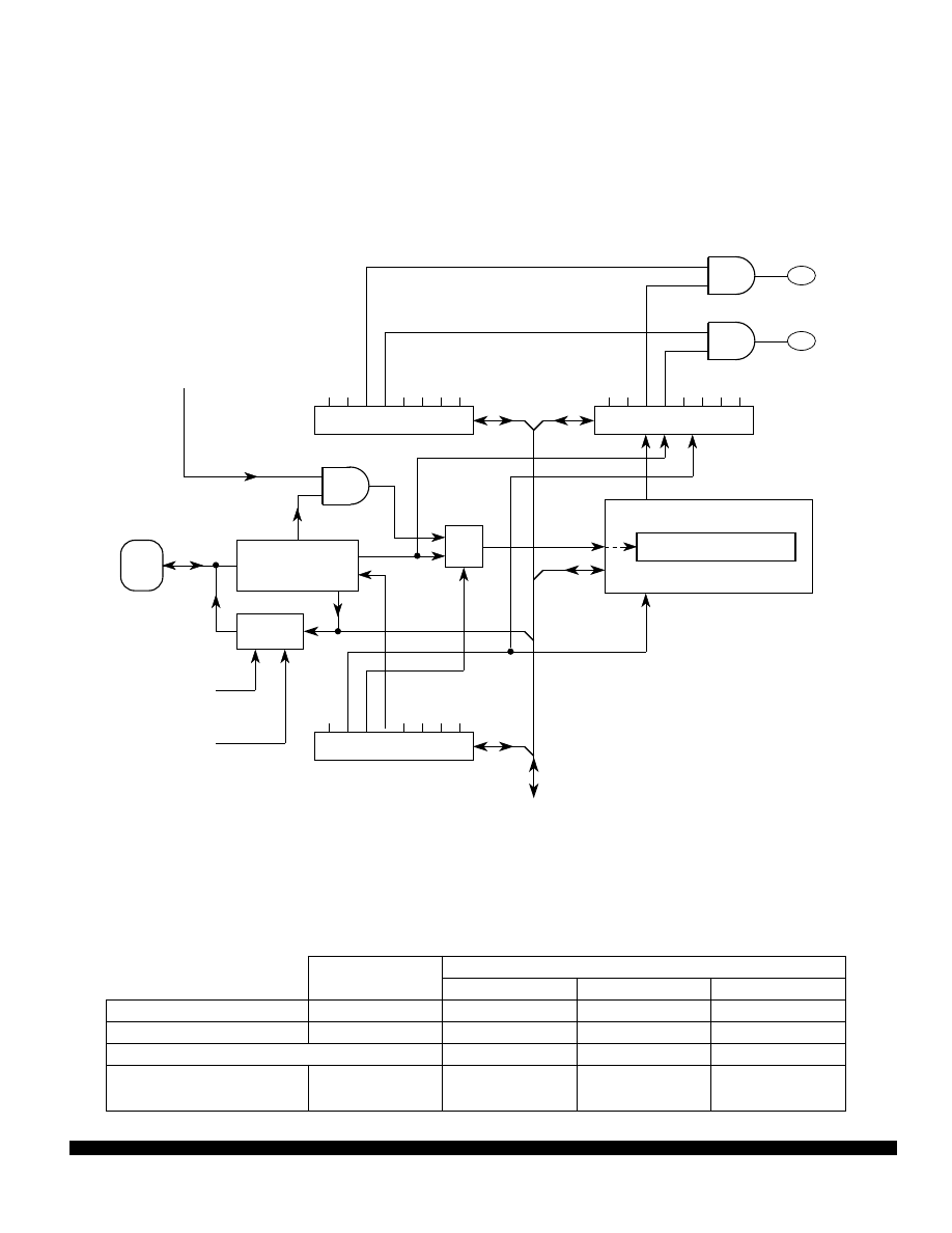
MOTOROLA
MC68HC11L6
40
BR774/D
10 Pulse Accumulator
The MC68HC11L6 has an 8-bit counter that can be configured to operate as a simple event counter or
for gated time accumulation, depending on the PAMOD bit in the PACTL register. The pulse accumu-
lator counter can be read or written at any time.
The port A bit 7 I/O pin can be configured as a clock in event counting mode or as a gate signal to enable
a free-running clock (E divided by 64) in gated accumulation mode.
Figure 12 Pulse Accumulator System Block Diagram
Table 8 Pulse Accumulator Timing
Common XTAL Frequencies
Selected Crystal
4.0 MHz
8.0 MHz
12.0 MHz
CPU Clock
(E)
1.0 MHz
2.0 MHz
3.0 MHz
Cycle Time
(1/E)
1000 ns
500 ns
333 ns
Pulse Accumulator (in Gated Mode)
(E/2
6
)
(E/2
14
)
1 count
overflow
64.0
µ
s
16.384 ms
32.0
µ
s
8.192 ms
21.33
µ
s
5.461 ms
OUTPUT
BUFFER
FROM
MAIN TIMER
OC1
FROM
DDRA7
PEDGE
PAMOD
PAEN
PACTL CONTROL
INTERNAL
DATA BUS
PACNT 8-BIT COUNTER
PA7/
PAI/
OC1
INTERRUPT
REQUESTS
PAIF
PAOVF
TFLG2 INTERRUPT STATUS
PAOVI
PAII
PAOVF
PAOVI
PAIF
PAII
TMSK2 INT ENABLES
1
2
OVERFLOW
ENABLE
DISABLE
FLAG SETTING
CLOCK
PAI EDGE
PAEN
PAEN
2:1
MUX
INPUT BUFFER
AND
EDGE DETECTOR
DATA BUS
PIN
E
÷
64 CLOCK
(FROM MAIN TIMER)
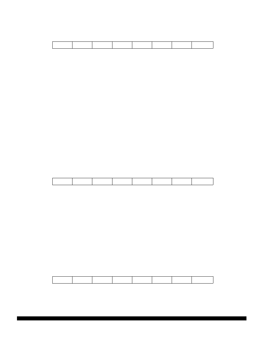
MC68HC11L6
MOTOROLA
BR774/D
41
TOI — Timer Overflow Interrupt Enable
(Refer to 9 Main Timer.)
RTII — Real-time Interrupt Enable
(Refer to 9 Main Timer.)
PAOVI — Pulse Accumulator Overflow Interrupt Enable
Set when pulse accumulator count rolls over from $FF to $00.
Cleared by writing to TFLG2 with a one in bit 4.
PAII — Pulse Accumulator Input Edge Interrupt Enable
Set each time a selected edge is detected at PA7/PAI/OC1.
Cleared by writing to TFLG2 with a one in bit 5.
NOTE
Bits in TMSK2 correspond bit for bit with flag bits in TFLG2. Ones in TMSK2 enable
the corresponding interrupt sources.
PR1 and PR0 — Timer Prescaler Select
(Refer to 9 Main Timer.)
Clear flags by writing a one to the corresponding bit position(s).
TOF — Timer Overflow Flag
(Refer to 9 Main Timer.)
RTIF — Real-Time (Periodic) Interrupt Flag
(Refer to 9 Main Timer.)
PAOVF — Pulse Accumulator Overflow Flag
Set when PACNT changes from $FF to $00.
PAIF — Pulse Accumulator Input Edge Flag
Set each time a selected active edge is detected on the PAI input line.
DDRA7 — Data Direction for Port A Bit 7
(Refer to 6 Parallel Input/Output.)
TMSK2 — Timer Interrupt Mask 2
$1024
Bit 7
6
5
4
3
2
1
Bit 0
TOI
RTII
PAOVI
PAII
0
0
PR1
PR0
RESET:
0
0
0
0
0
0
0
0
TFLG2 — Timer Interrupt Flag 2
$1025
Bit 7
6
5
4
3
2
1
Bit 0
TOF
RTIF
PAOVF
PAIF
0
0
0
0
RESET:
0
0
0
0
0
0
0
0
PACTL — Pulse Accumulator Control
$1026
Bit 7
6
5
4
3
2
1
Bit 0
DDRA7
PAEN
PAMOD
PEDGE
DDRA3
I4/O5
RTR1
RTR0
RESET:
0
0
0
0
0
0
0
0
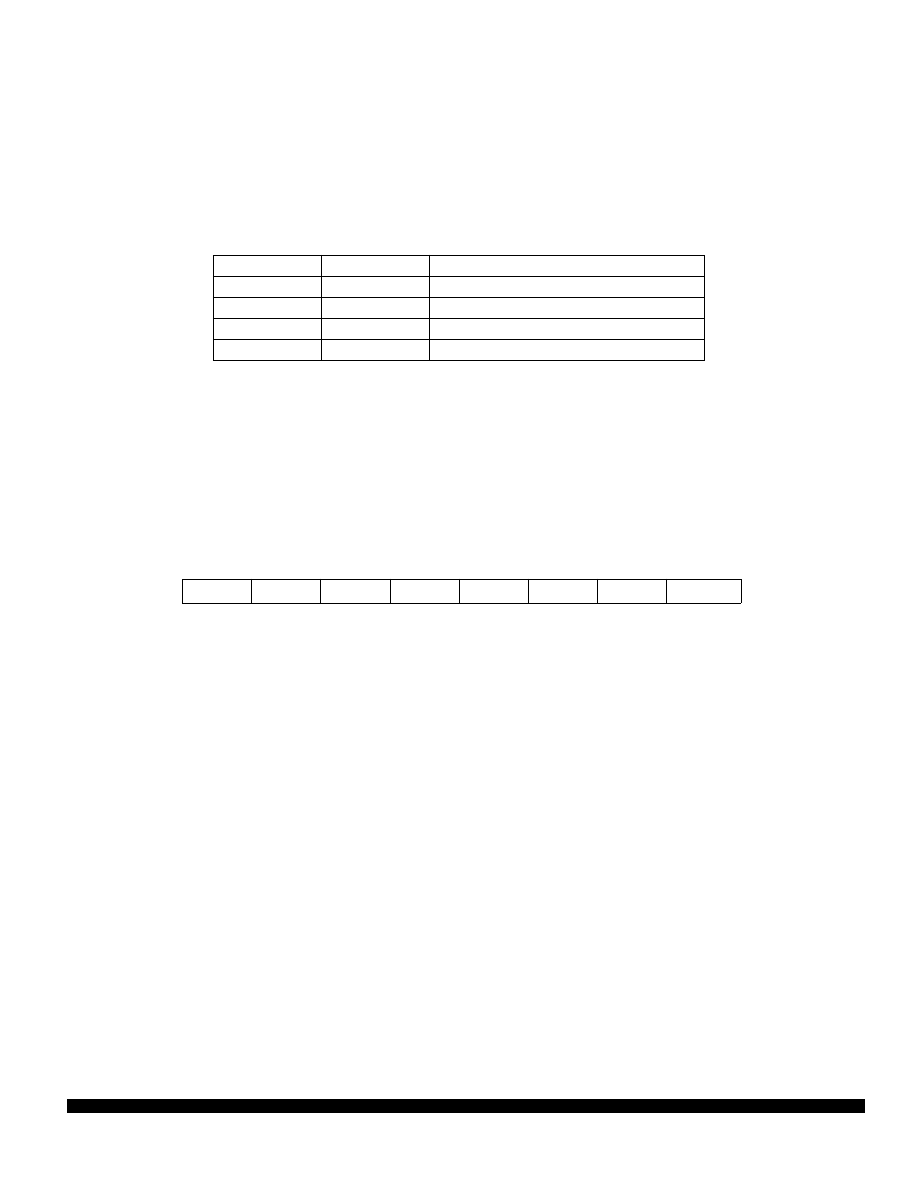
MOTOROLA
MC68HC11L6
42
BR774/D
PAEN — Pulse Accumulator System Enable
0 = Pulse Accumulator disabled
1 = Pulse Accumulator enabled
PAMOD — Pulse Accumulator Mode
0 = Event counter
1 = Gated time accumulation
PEDGE — Pulse Accumulator Edge Control
DDRA3 — Data Direction for Port A Bit 3
(Refer to 6 Parallel Input/Output)
I4/O5 — Input Capture 4/Output Compare 5
(Refer to 6 Parallel Input/Output)
RTR1 and RTR0 —
(Refer to 9 Main Timer.)
Can be read and written.
PAMOD
PEDGE
Action on Clock
0
0
PAI falling edge increments the counter
0
1
PAI rising edge increments the counter
1
0
A zero on PAI inhibits counting
1
1
A one on PAI inhibits counting
PACNT — Pulse Accumulator Counter
$1027
Bit 7
6
5
4
3
2
1
Bit 0
Bit 7
6
5
4
3
2
1
Bit 0
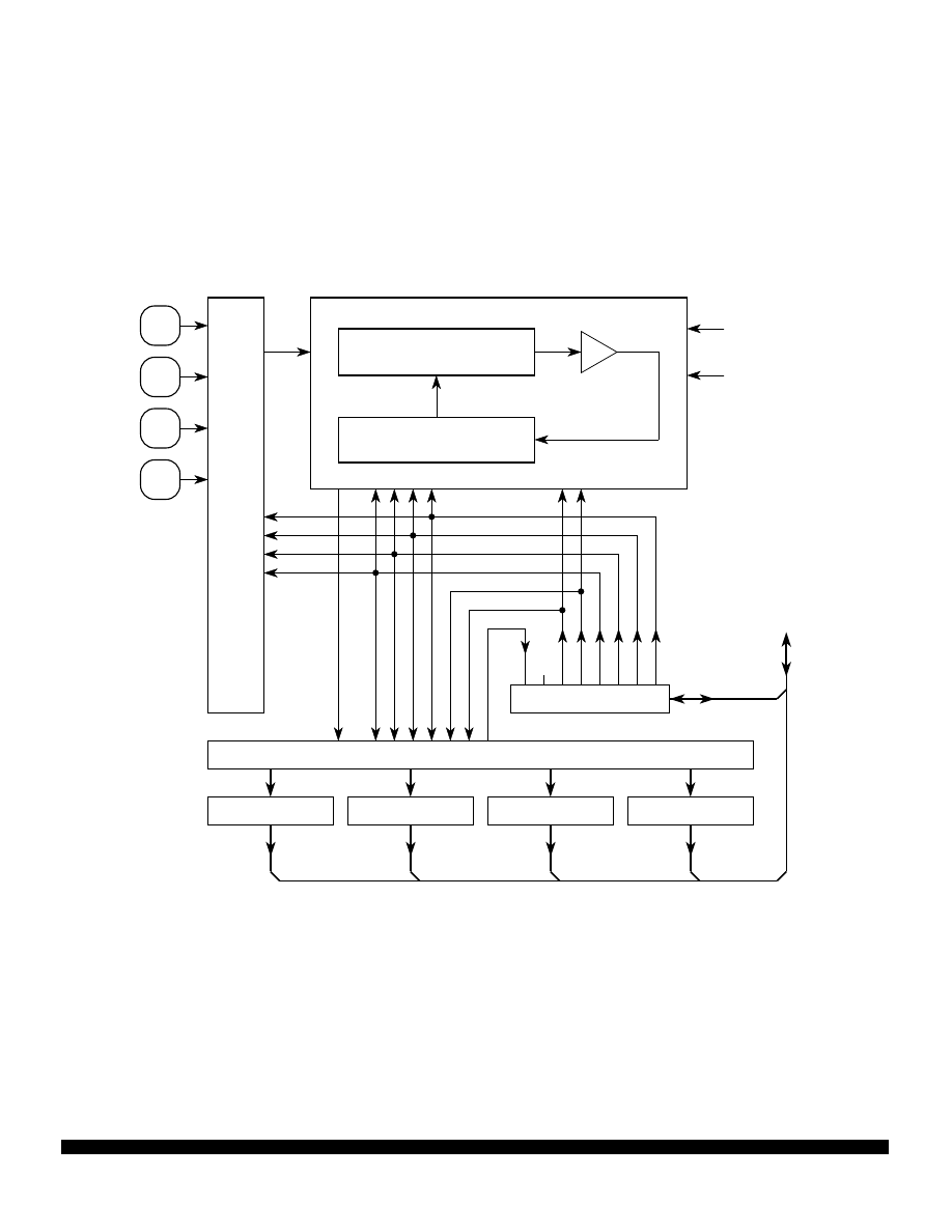
MC68HC11L6
MOTOROLA
BR774/D
43
11 A/D Converter
The A/D converter system uses an all-capacitive charge-redistribution technique to convert analog sig-
nals to digital values. The MC68HC11L6 A/D system, an 8-channel, 8-bit, multiplexed-input, succes-
sive-approximation converter, is accurate to
±
1 least significant bit (LSB). It does not require external
sample and hold circuits because of the type of charge-redistribution technique used.
Dedicated lines V
RH
and V
RL
provide the reference supply voltage inputs.
A multiplexer allows the single A/D converter to select one of 16 analog signals.
Figure 13 A/D Converter Block Diagram
PE0/
AN0
PE1/
AN1
PE2/
AN2
PE3/
AN3
ANALOG
MUX
8-BIT CAPACITIVE DAC
WITH SAMPLE AND HOLD
SUCCESSIVE APPROXIMATION
REGISTER AND CONTROL
ADCTL A/D CONTROL
CB
CC
CD
MULT
SCAN
CCF
CA
ADDR 3 A/D RESULT 3
RESULT REGISTER INTERFACE
RESULT
INTERNAL
DATA BUS
VRH
VRL
ADDR 4 A/D RESULT 4
ADDR 2 A/D RESULT 2
ADDR 1 A/D RESULT 1
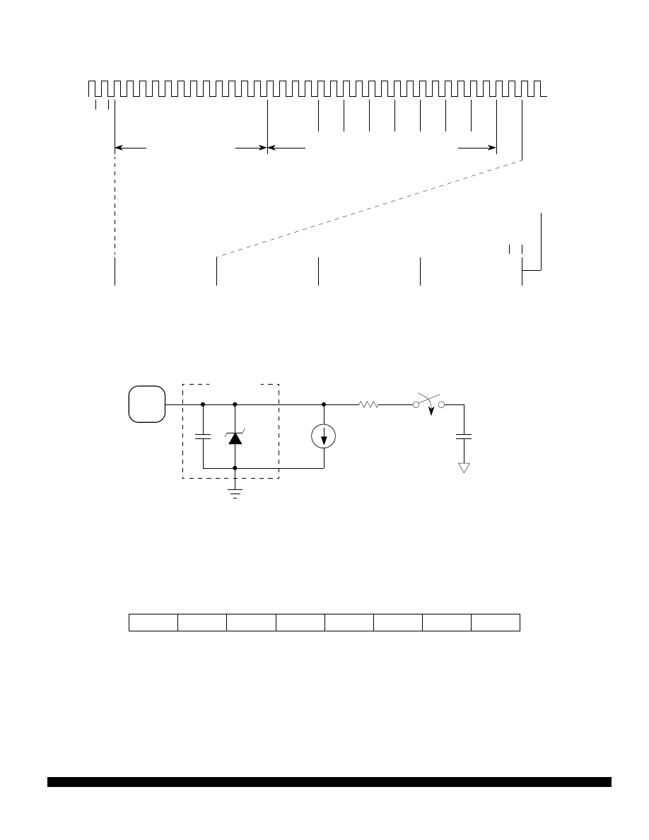
MOTOROLA
MC68HC11L6
44
BR774/D
Figure 14 A/D Conversion Sequence
Figure 15 Electrical Model of an Analog Input Pin (Sample Mode)
CCF — Conversions Complete Flag
Set after the fourth conversion in an A/D conversion cycle, cleared when ADCTL is written
SCAN — Continuous Scan Control
0 = Do four conversions and stop
1 = Convert four channels in selected group continuously
ADCTL — A/D Control/Status
$1030
Bit 7
6
5
4
3
2
1
Bit 0
$1030
CCF
0
SCAN
MULT
CD
CC
CB
CA
RESET:
0
0
U
U
U
U
U
U
MSB
4
CYCLES
E CLOCK
WRITE
BIT 6
2
CYC
BIT 5
2
CYC
BIT 4
2
CYC
BIT 3
2
CYC
BIT 2
2
CYC
BIT 1
2
CYC
LSB
2
CYC
END
12 E CYCLES
SAMPLE ANALOG INPUT
SUCCESSIVE APPROXIMATION SEQUENCE
2
CYC
CONVERT FOURTH
CHANNEL
AND UPDATE ADDR4
CONVERT THIRD
CHANNEL
AND UPDATE ADDR3
CONVERT SECOND
CHANNEL
AND UPDATE ADDR2
CONVERT FIRST
CHANNEL
AND UPDATE ADDR1
SET
REPEAT
E
CYCLES
128
96
64
32
0
TO
ADCTL
SEQUENCE
IF
SCAN = 1
CCF
FLAG
DAC
CAPACITANCE
VRL
ANALOG
INPUT
PIN
~
20 pF
+
~
20 V
–
~
0.7 V
< 2 pF
INPUT
PROTECTION
DEVICE
400 nA
JUNCTION
LEAKAGE
DIFFUSION AND
POLY COUPLER
≤
4 k
Ω
*
This analog switch is closed only during the 12-cycle sample time.
*
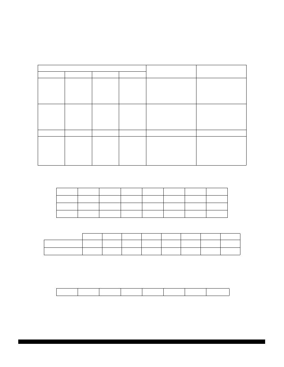
MC68HC11L6
MOTOROLA
BR774/D
45
MULT — Multiple Channel/Single Channel Control
0 = Convert single channel selected
1 = Convert four channels in selected group
CD–CA — Channel Select D through A
*Used for factory testing
*Can be written only once in first 64 cycles out of reset in normal modes, or at any time in special modes.
ADPU — A/D Power Up
0 = A/D Powered down
1 = A/D Powered up
Table 9 A/D Converter Channel Assignments
Channel Select Control Bits
Channel
Result in ADRx if
CD
CC
CB
CA
Signal
MULT = 1
0
0
0
0
AN0
ADR1
0
0
0
1
AN1
ADR2
0
0
1
0
AN2
ADR3
0
0
1
1
AN3
ADR4
0
1
0
0
AN4
ADR1
0
1
0
1
AN5
ADR2
0
1
1
0
AN6
ADR3
0
1
1
1
AN7
ADR4
1
0
X
X
Reserved
—
1
1
0
0
V
RH*
ADR1
1
1
0
1
V
RL*
ADR2
1
1
1
0
(V
RH
)/2
*
ADR3
1
1
1
1
Reserved
*
ADR4
ADR1–ADR4 — A/D Results
$1031–$1034
$1031
Bit 7
6
5
4
3
2
1
Bit 0
ADR1
$1032
Bit 7
6
5
4
3
2
1
Bit 0
ADR2
$1033
Bit 7
6
5
4
3
2
1
Bit 0
ADR3
$1034
Bit 7
6
5
4
3
2
1
Bit 0
ADR4
Table 10 Analog Input to 8-Bit Result Translation Table
Bit 7
6
5
4
3
2
1
Bit 0
%
(1)
50%
25%
12.5%
6.25%
3.12%
1.56%
0.78%
0.39%
Volts
(2)
2.500
1.250
0.625
0.3125
0.1562
0.0781
0.0391
0.0195
(1)
% of V
RH
–V
RL
(2)
Volts for V
RL
= 0; V
RH
= 5.0 V
OPTION — System Configuration Options
$1039
Bit 7
6
5
4
3
2
1
Bit 0
ADPU
CSEL
IRQE*
DLY*
CME
0
CR1*
CR0*
RESET:
0
0
0
1
0
0
0
0

MOTOROLA
MC68HC11L6
46
BR774/D
CSEL — Clock Select
0 = A/D and EEPROM use system E clock
1 = A/D and EEPROM use internal RC clock
IRQE — IRQ Select Edge Sensitive Only
(Refer to 4 Resets and Interrupts.)
DLY — Enable Oscillator Start-Up Delay on Exit from STOP
(Refer to 4 Resets and Interrupts.)
CME — Clock Monitor Enable
(Refer to 4 Resets and Interrupts.)
CR1, CR0 — COP Timer Rate Select
(Refer to 4 Resets and Interrupts.)

MC68HC11L6
MOTOROLA
BR774/D
47

Motorola reserves the right to make changes without further notice to any products herein. Motorola makes no warranty, representation or guarantee regarding
the suitability of its products for any particular purpose, nor does Motorola assume any liability arising out of the application or use of any product or circuit, and
specifically disclaims any and all liability, including without limitation consequential or incidental damages. “Typical” parameters can and do vary in different
applications. All operating parameters, including “Typicals” must be validated for each customer application by customer’s technical experts. Motorola does not
convey any license under its patent rights nor the rights of others. Motorola products are not designed, intended, or authorized for use as components in
systems intended for surgical implant into the body, or other applications intended to support or sustain life, or for any other application in which the failure of
the Motorola product could create a situation where personal injury or death may occur. Should Buyer purchase or use Motorola products for any such
unintended or unauthorized application, Buyer shall indemnify and hold Motorola and its officers, employees, subsidiaries, affiliates, and distributors harmless
against all claims, costs, damages, and expenses, and reasonable attorney fees arising out of, directly or indirectly, any claim of personal injury or death
associated with such unintended or unauthorized use, even if such claim alleges that Motorola was negligent regarding the design or manufacture of the part.
Motorola and
B
are registered trademarks of Motorola, Inc. Motorola, Inc. is an Equal Opportunity/Affirmative Action Employer.
How to reach us:
USA/EUROPE: Motorola Literature Distribution;
P.O. Box 20912; Phoenix, Arizona 85036. 1-800-441-2447
MFAX: RMFAX0@email.sps.mot.com - TOUCHTONE (602) 244-6609
INTERNET: http://Design-NET.com
JAPAN: Nippon Motorola Ltd.; Tatsumi-SPD-JLDC, Toshikatsu Otsuki,
6F Seibu-Butsuryu-Center, 3-14-2 Tatsumi Koto-Ku, Tokyo 135, Japan. 03-3521-8315
HONG KONG: Motorola Semiconductors H.K. Ltd.; 8B Tai Ping Industrial Park,
51 Ting Kok Road, Tai Po, N.T., Hong Kong. 852-26629298
M
Document Outline
- 1 Introduction
- 2 Features
- 3 Operating Modes and Memory Maps
- 4 Resets and Interrupts
- 5 Electrically Erasable Programmable Read-Only Mem...
- 6 Parallel Input/Output
- 7 Serial Communications Interface (SCI)
- 8 Serial Peripheral Interface (SPI)
- 9 Main Timer
- 10 Pulse Accumulator
- 11 A/D Converter
Wyszukiwarka
Podobne podstrony:
MC68HC11KA Technical Summary
NOTAKI Z TECHNIKI CYFROWEJ
techniki inchalacyjne
Mechanika techniczna(12)
W6 Technika harmonogramów i CPM
01 Podstawy i technika
Techniki unieszkodliwiania odpadów
techniki informacyjne
TECHNIKAa
Normy techniczne
TECHNIKA ROLNICZA literatura
PIT wyklad 1 planowanie infrastuktury technicznej
W11 Scinanie czyste i techniczne
20 Rysunkowa dokumentacja techniczna
3[1] c c wskazania technika
techniczne srodki zabezpieczenia(1)
sieci Techniki komutacji
Techniki ochrony gleb i gruntów przed erozją
więcej podobnych podstron