CONTENTS
1. General Intro d u c t i o n
2. Specification
3. NAM Pro g r a m m i n g
4. Data Tr a n s f e r
5. Circuit Description
6. Exploded View and Its Parts List
7. PCB Diagrams
8. Tro u b l e s h o o t i n g
9. Test Command Ta b l e
10. Block & Circuit Diagrams
CDMA Portable Cellular Telephone
SERVICE
Manual
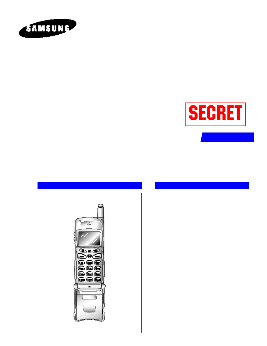
SCH-570
CDMA Portable
Cellular Telephone

Samsung Electronics Co.,Ltd. SEP. 1998.
Printed in Korea
Code No. : GH68-60724A
HONGKONG CHINA.

1-1
1. General Introduction
The SCH-570 cellular phone functions as only digital cellular phone working in CDMA (Code Division
Multiple Access) mode. CDMA type digital mode applies DSSS (Direct Sequential Spread spectrum) mode
which first came to be used in the military.
The DSSS reduces channel cross talk and allow to use one frequency channel by multiple users in the same
specific area, resulting in increase of channel capacity to about ten times compared to that of analog mode
currently used.
Soft/Softer Handoff, Hard Handoff, and Dynamic RF Power Control technologies are combined into this
phone to reduce the call drop while usage.
CDMA digital cellular network consists of MSO (Mobile Switching Office), BSC (Base Station Controller),
BTS (Base Station Transmission System), and MS (Mobile Station). MS meets the specifications of the below:
IS-95A : Mobile Station-Base Station Compatibility Standard for Dual-Mode Wideband Spread Spectrum
Cellular System
IS-96A : Speech Service Option 1 Standard for Dual-Mode Wideband Spread Spectrum Cellular Systems
IS-98A : Standards for Dual-Mode Wideband Spread Spectrum Cellular Mobile Station
IS-126 : Mobile Station Loopback Service Options Standard
SCH-570 is composed of main handset, desktop charger, standard battery.
1-2
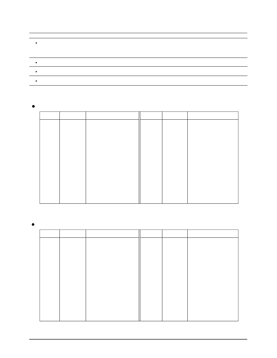
1.1 General
Frequency Range
Transmitter
: 824.64 ~ 848.37 MHz
Receiver
: 869.64 ~ 893.37 MHz
Channel Spacing
: 1.23 MHz
Number of Channels
: 20 FA
Duplex Spacing
: 45 MHz
MSC Transmitter Frequency
FA NO.
CH. NO.
CENTER FREQUENCY
FA NO.
CH. NO.
CENTER FREQUENCY
1
1011
824.640MHz
11
404
837.120MHz
2
29
825.870MHz
12
445
838.350MHz
3
70
827.100MHz
13
486
839.580MHz
4
111
828.330MHz
14
527
840.810MHz
5
152
829.560MHz
15
568
842.040MHz
6
193
830.790MHz
16
609
843.270MHz
7
234
832.020MHz
17
650
844.270MHz
8
275
833.250MHz
18
697
845.910MHz
9
316
834.480MHz
19
738
847.140MHz
10
363
835.890MHz
20
779
848.370MHz
MSC Receiver Frequency
FA NO.
CH. NO.
CENTER FREQUENCY
FA NO.
CH. NO.
CENTER FREQUENCY
1
1011
869.640MHz
11
404
882.120MHz
2
29
870.870MHz
12
445
883.350MHz
3
70
872.100MHz
13
486
884.580MHz
4
111
873.330MHz
14
527
885.810MHz
5
152
874.560MHz
15
568
887.040MHz
6
193
875.790MHz
16
609
888.270MHz
7
234
877.020MHz
17
650
889.270MHz
8
275
878.250MHz
18
697
890.910MHz
9
316
879.480MHz
19
738
892.140MHz
10
363
880.890MHz
20
779
893.370MHz
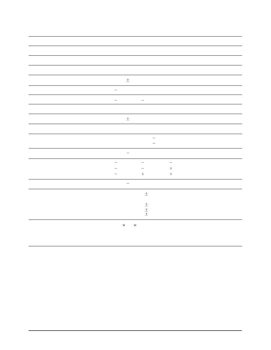
2. Specification
Frequency Range Transmitter
: 824.64 MHz ~ 848.37MHz
Frequency Range Receiver
: 869.64 MHz ~ 893.37 MHz
Waveform Quality
: above 0.944
Time Reference
: within
1uS
RX Sensitivity
:
104 dBm, FER = within 0.5%
Dynamic Range
:
104 dBm ~
25 dBm, FER = within 0.5%
TX Output Power
: Maximum 320 mW (25dBm)
TX Frequency Deviation
: within
300 Hz
Occupied Band Width
: 1.32 MHz
TX Conducted Spurious Emissions
: 900 kHz below
42 dBc / 30 kHz
: 1.98 MHz below
54 dBc / 30 kHz
Minimum TX Power Control
: below
50 dBm
Open Loop Power Control
:
25 dBm :
57.0 dBm ~
38.5 dBm
65 dBm :
17.5 dBm ~
1.5 dBm
104 dBm :
18.0 dBm ~
30.0 dBm
Stand-by Output Power
: below
61 dBm
Closed Loop TX Power Control Range
: Test 1 within
24 dB
Test 2 0 ms ~ 2.5 ms
Test 3 within
24 dB
Test 4 within
24 dB
Test 5 within
24 dB
Size (mm)
: 108
46
25 (Standard battery)
Weight (g)
: 128 (1000mA Standard battery)
2-1

5-1
5. Circuit Description
5-1 Logic Section
5-1-1 Power Supply
With the battery installed on the phone and by
pressing the END/ key, the VBATT and
ON_SW signals will be connected. This will turn
on U123 DC_DC convertor.
This in turn will be supplied to PIN3, PIN4 of
regulators U124, PIN6 of regulators U122, thus
releasing them from the shut-down state to output
regulated 3.3V. ( The VBATT applied to ON-SW
will turn on Q103(DTC144EE) resulting in the
signal ON_SW_SENSE to change the start from
High to Low.)
The MSM recognizes this signal and sends out
PS_HOLD (logical HIGH) to turn on Q102 even
after the PWR key is released.
The power from U124 is used in the digital part of
MSM and BBA. The power from U122 is used in
analog part of BBA.
5-1-2 Logic Part
The logic part consists of internal CPU of MSM,
RAM, ROM and EEPROM. The MSM receives
TCXO and CHIPX8 clock signals from the BBA
and controls the phone during the operation. The
major components are as follows:
CPU
: INTEL 80186 core (inside the MSM)
FLASH ROM : U701 - 8 Mbit FLASH MEMORY
SRAM
: U703 - 2 Mbit STATIC RAM
FLASH ROM : U702 - 1 Mbit FLASH MEMORY
EEPROM : U102 - 128 Kbit SERIAL EEPROM
CPU
INTEL 80186 CMOS type 16-bit microprocessor is
used for the main processing. The CPU controls all
the circuitry. For the CPU clock, 27MHz resonator
is used.
FLASH ROM
One 8 MBIT FROM is used to store the terminal's
program. Using the down-loading program, the
program can be changed even after the terminal is
fully assembled.
SRAM
One 2 MBIT SRAM is used to store the internal
flag information, call processing data, and timer
data.
EEPROM
One 128 KBIT EEPROM is used to store ESN,
NAM, power level, volume level, and telephone
number.
KEYPAD
For key recognition, key matrix is to set up using
SCAN0-6 of STORE signals and KEY0-3 of input
ports of MSM. Ten LEDs and backlighting
circuitry are included in the keypad for easy
operation in the dark.
LCD MODULE
LCD module contains a controller which will
display the information onto the LCD by 8-bit data
from the MSM. It also consists a DC-DC converter
to supply -3.5V for fine view angle and LCD
reflector to improve the display efficiency.

5-2
5-1-3 Baseband Part
MOBILE STATION MODEM (MSM)
The MSM equipped with the INTEL 80186 CPU
core is an important component of the CDMA
cellular phone. The MSM comes in a 176 pins
TQFP package.
MICROPROCESSOR INTERFACE
The interface circuitry consists of reset circuit,
address bus (A0-A19), data bus (AD0-AD15), and
memory controls (ALE, DT_R, HWR/, LWR/,
RAM_CS/, ROM_CS etc).
INPUT CLOCK
CPU clock: 27 MHz
TCXO/4 (pin 34): 4.92 MHz. This clock signal
from the BBA is the reference clock for the MSM
except in CDMA mode.
CHIPX8 : 9.8304 MHz. The reference clock used
during the CDMA mode.
BBA INTERFACE
CDMA, FM Data Interface
TXIQDATA0-7 (pins 24-32) : TX data bus used
during both CDMA and FM mode but it is used
only for CDMA mode at this phone.
Clock
TC_CLK (pin 22), TX_CLK/(pin 23) : Digital to
Anolog Converter (DAC) reference clock used in
CDMA TX mode.
CHIPX8 : ADC reference clock used in CDMA
RX mode.
ADC Interface
ADC_CLK (pin 3), ADC_ENABLE (pin 1) and
ADC_DATA (pin 2) are required to control the
internal ADC in the BBA.
Data Port Interface
Includes the UART. Also, supports Diagnostic
Monitor (DM), HP equipment interface, down
loading, and data service.
CODEC Interface
The MSM sends 2.048 MHz PCM_CLK (pin 19)
and 8 KHz PCM_SYNC (pin 16, 20) to the CODEC
(U117). The voice PCM data from the MSM (U101)
PCM_DIN (pin 135) is compressed into 8 KHz, by
QCELP algorithm in the CDMA mode.
RF Interface
TX : TX_AGC_ADJ (pin 35) port is used to control
the TX power level and PA_ON (pin 44) signal is
used to control the power amplifier. This signal
depends on the TX vocoder rate.
RX : AGC_REF (pin 36) port is used to control the
RX gain and TRK_LO_ADJ (pin 45) is used to
compensate the TCXO clock.
General Purpose I/O Register Pins
Input/output ports to control external devices.
Power Down Control
When the IDLE/ signal turns to LOW, only the TX
sections will be disabled. If both the IDLE/ and
SLEEP/ change to LOW, all the pins except for the
TCXO and 27MHz clock are disabled.

5-1-4 Audio Part
TX AUDIO PATH
The voice signal output from microphone is
filtered and amplified by the internal OP-AMP
and is converted to PCM data by the CODEC
(U117). The signal is then applied to the MSM
(U101)’s internal vocoder.
RX AUDIO PATH
The PCM data from the MSM’s converted to audio
signal by ADC of CODEC (U117), is then
amplified by the speaker amplifer (U111) to be
sent to the speaker unit.
TX WBD, ST,SAT
These signals are generated from MSM. The
modulation level of TX WBD and ST is 8
kHz/dev, and SAT is
2 kHz/dev.
BUZZER DRIVING CIRCUITRY
Buzzer generates alert tone when the buzzer
receives the timer signal from the MSM, it
generates alert tone. The buzzer level is adjusted
by the alert signal’s period generated from the
MSM timer.
KEY TONE GENERATION
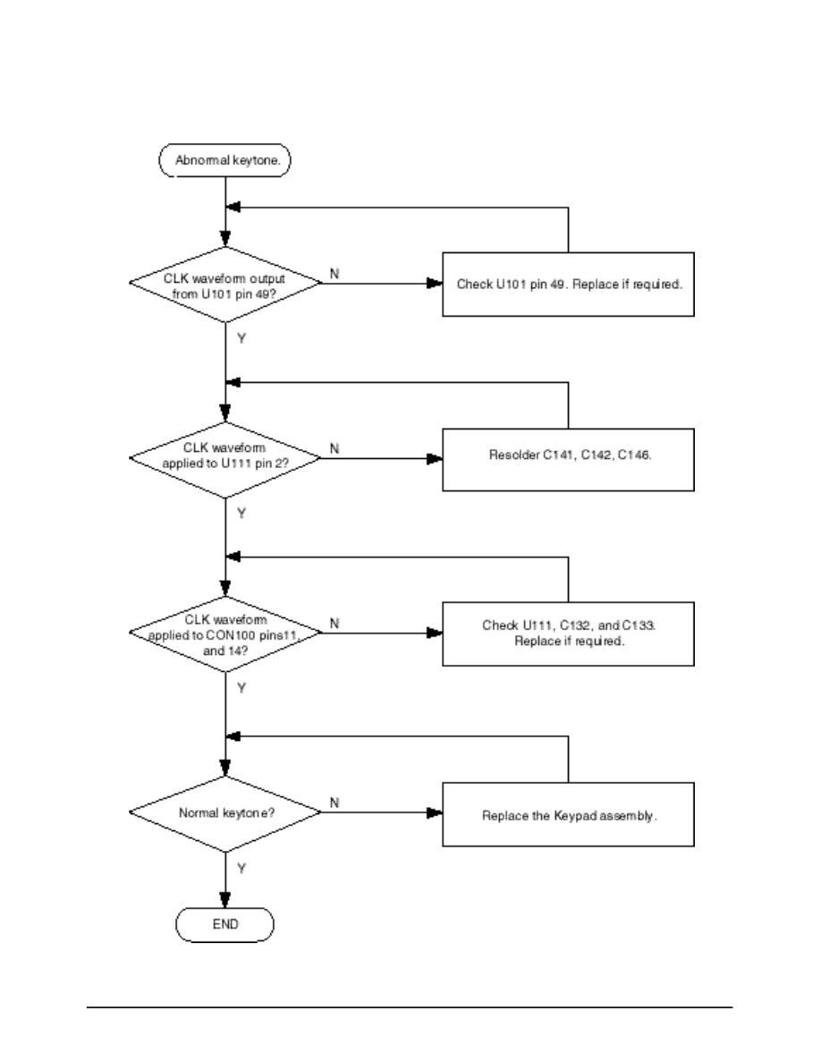
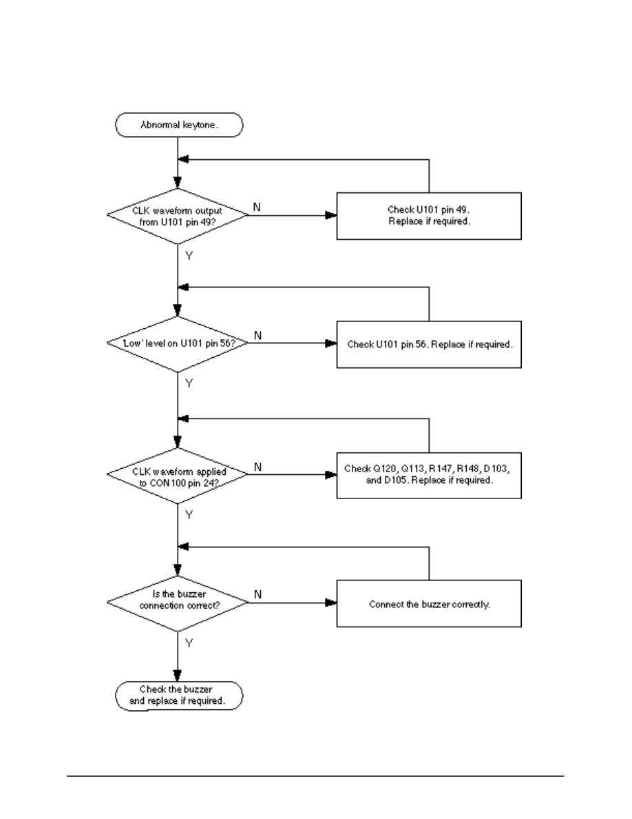
Ringer signal (pin49) out from MSM (U101) is
passed through 2 serial LPF consisting of R141,
C146, R145, and C142 amplified at the speaker
amp (U111), and comes out to speaker.
5-3

5-4
5-2 Receiver Section
LOW NOISE AMPLIFIER (LNA, Q302)
The low noise amplifier amplifies a weak signal
received from the base station to obtain the
optimum level (Noise figure = 1.5 dB,
Gain = 16 dB).
RADIO FREQUENCY BAND PASS FILTER
(RF BPF, F302)
The RF BPF accepts only a specific frequency (881
12.5 MHz) from the signal received from the
base station. The band width is 25 MHz.
DOWN CONVERTER (MIXER, U301)
First local signal is applied to this down converter.
The down converter transfers the signal amplified
at the LNA into 85.38 MHz IF signal. 85.38 MHz IF
signal is made by subtracting 881 12.5 MHz RF
signal from 966 12.5 MHz first local signal.
AUTOMATIC GAIN CONTROLLER (AGC)
AMP (Q302)
85.38 MHz IF signal is applied to IF AGC amp, the
IF AGC output level is applied to BBA (Baseband
Analog ASIC). The IF AGC amp (Q302) keeps the
signal at a constant level by controlling the gain.
Dynamic range is 90dB, up gain +45dB, and down
gain -45dB.
IF SAW BAND PASS FILTER (FOR CDMA)
IF SAW BPF (F303) is used for CDMA system
having 1.23 MHz wideband and 630 kHz
bandwidth. The filter also attenuates the image
product generated at the mixer.
BUFFER AMP (Q304)
Buffer (Q304) amplifiers signal to be applied to the
local input of the down converter (U301) when a
phase is locked between VCO (U341) and PLL IC
(U342).

5-5
VOLTAGE CONTROLLED OSCILLATOR (VCO,
U341)
The VCO (U341) generates the signal having 966
MHz center frequency and 12.5 MHz deviation
with the voltage control. PLL IC (U342) controls
this signal.
ANTENNA
Antenna allows signals and sends to receive from
the base station.
PHASE LOCKED LOOP (PLL, U342)
Input reference frequency is generated at
VC_TCXO (U343) and the divided signal is
generated at VCO. PLL compares the two signals
and generates the desired signal with a pre-
programmed counter which controls voltage.
VOLTAGE CONTROLLED TEMPERATURE
COMPENSATED CRYSTAL OSCILLATOR (VC-
TCXO, U343)
It provides 19.68 MHz reference frequency to PLL.
A correct frequency tuning is made by the voltage
control.
DUPLEXER (F301)
Duplexer (F301) controls to transmit through the
antenna only the signals within acceptable Tx
frequency range (836 12.5 MHz) and to receive
through the antenna only the signals within
acceptable Rx frequency range (881 12.5 MHz).
It also matches LNA input in receiving part and
PA output in transmitter part with the antenna.
POWER SUPPLY REGULATOR (U123)
The power supply regulator generates a regulated
power.
THERMISTOR (R498)
The thermistor (R498) detects temperature. It is
used to compensate active component
characteristics due to the temperature difference.

5-6
5-3 Transmitter Section
BBA (U401)
BBA (U401) consists of ADC, DAC, LPF (CDMA),
divider, VCO, logic control circuit, PLL, and mixer.
BBA performs a specific function between RF part
and logic part, with MSM. The IF signal out from
Rx IF AGC amp is secondly converted through the
down-converter. The signal passes through the
CDMA or FM filter, converts to digital signal
through ADC, then is sent to MSM. The digital
signal out from MSM converts to analog signal
through each filter and the up-converters.
POWER AMP MODULE (U467)
Power Amp module (U467) amplifies signal (24dB
Gain) to be sent out to the base station through the
antenna.
UP CONVERTER (MIXER, U460)
The up-converter (U460) receives the first local
signal to generate 836 12.5 MHz from the BBA.
836 12.5 MHz signal comes out of the mixer
output by subtracting 130 MHz IF signal from 966
12.5 MHz first local signal.
RF AUTOMATIC GAIN CONTROLLER AMP
(U461, U464)
The signal out to the base station should be a
constant level. The TX RF AGC amp controls
power to keep the signal at a constant level.
RF BAND PASS FILTER (BPF, F451)
The RF BPF ( F451) accepts only a specific
frequency (836 12.5MHz) to send it out to the
base station. The band width is 25 MHz.
POWER SUPPLY SWITCHING (U484)
Power supply switching (U484) turns on
TX_POWER when the phone is in traffic mode and
supplies power to the circuits.
POWER SUPPLY REGULATOR (U482, U483)
The power supply regulators (U482,U483) supply
a regulated power to each part of transmitter.
U482 supplies 3.6V to TX AGC amp (U461) and
up-converter (U460). U483 supplies 3.0V to power
amp module control circuit (U487).
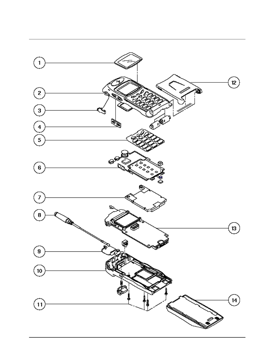
6-1
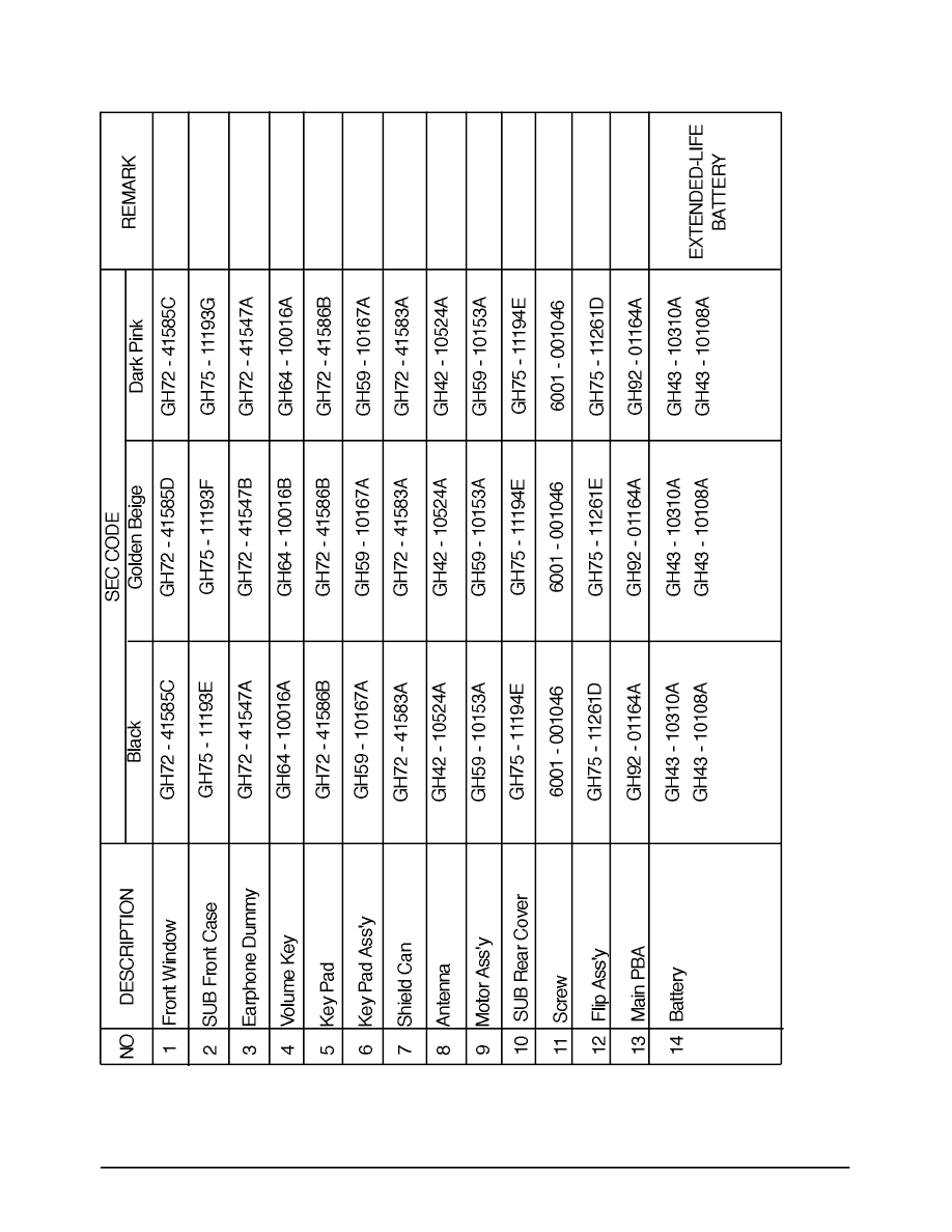
6-1 Fixed Phone Exploded View
6. Exploded View and its Parts List
6-2
6-2 Fixed Phone Parts List

6-3
6-3 Rapid Charger View
SEC CODE : GH44 - 40100A
7. PCB Diagrams
7-1 Cellular Phone
7-1
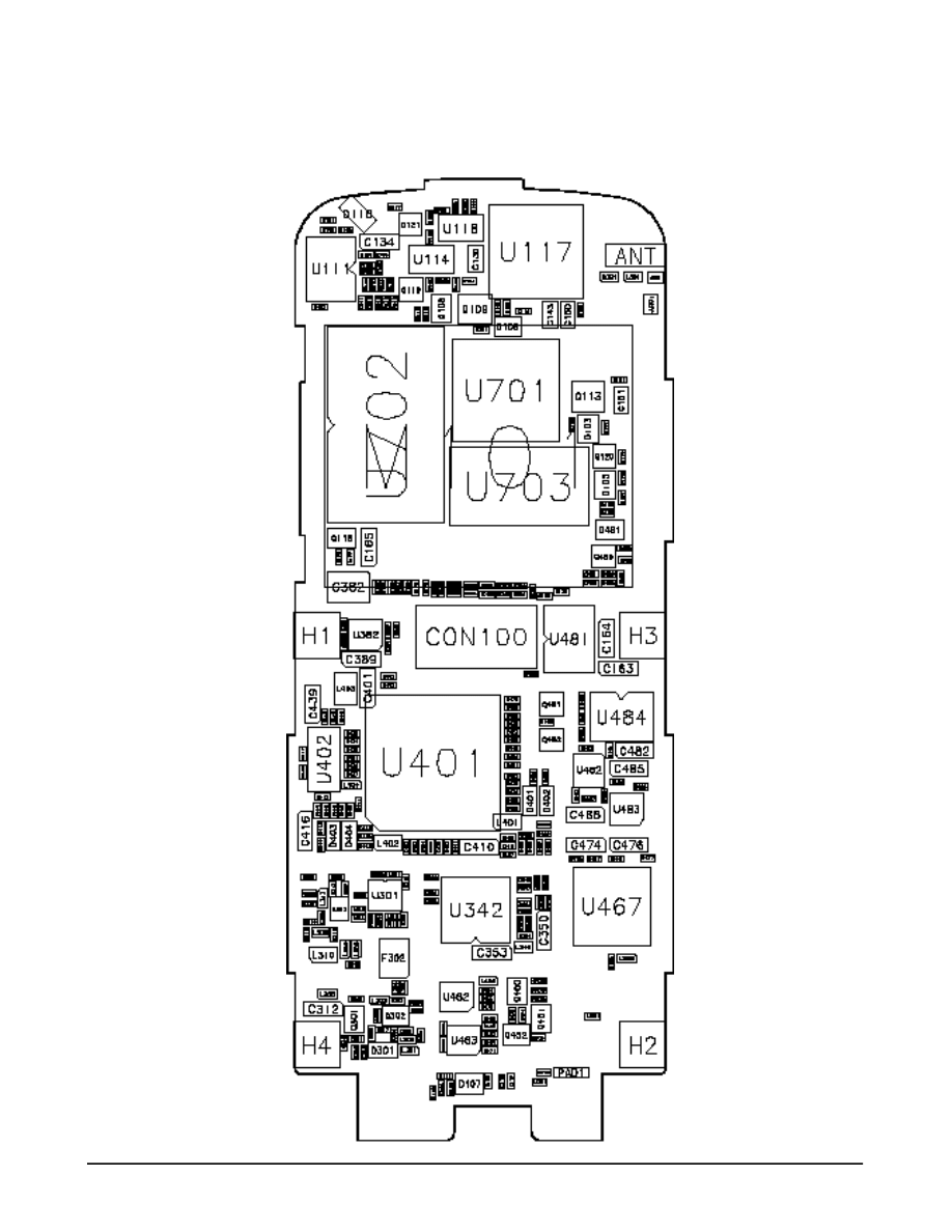
7-1-1 Main Board PCB: Top
7-2
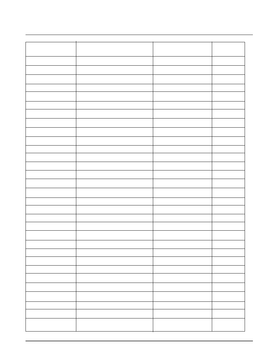
7-1-2 Main Board PCB: Bottom
7-3
7-2 Electrical Parts List
SEC CODE
DESCRIPTION
PART NO.
REMARK
0401 - 001052
DIODE - SWITCHING
D101 D109
0405 - 000107
DIODE - VARACTOR
D401 D402 D403 D404
0407 - 000115
DIODE - ARRAY
D103 D105 D106
0407 - 000122
DIODE - ARRAY
D102 D104
0407 - 000127
DIODE - ARRAY
D107 D108 D481
0409 - 000108
DIODE - PIN
D301
0501 - 000162
TR - SMALL SIGNAL
Q116 Q450 Q452
0501 - 000218
TR - SMALL SIGNAL
Q102 Q108 Q114 Q301
0501 - 000218
TR - SMALL SIGNAL
Q451
0501 - 000457
TR - SMALL SIGNAL
Q113 Q115
0501 - 000689
TR - SMALL SIGNAL
Q304
0501 - 002063
TR - SMALL SIGNAL
Q303
0501 - 002208 TR - SMALL SIGNAL Q109
0504 - 000167
TR - DIGITAL
Q119 Q481 Q482
0504 - 000168
TR - DIGITAL
Q103 Q121
0504 - 000172
TR - DIGITAL
Q111 Q120
0504 - 001016
TR - DIGITAL
Q485
0501 - 001062
FET - GaAs
U301
0505 - 001095
FET - SILICON
U106
0505 - 001119
FET - SILICON
Q302
0505 - 001165
FET - SILICON
U104
0505 - 001170
FET - SILICON
U484
0601 - 000355
LED - CHIP - RED
D116
0801 - 000304
IC - CMOS - LOGIC
U105
0803 - 003010
IC - TTL
U114
0904 - 001183
IC - DSP
U201
1001 - 001019
IC - ANALOG MULTIPLEX
U481
1103 - 001062
IC - EEPROM
U102
1106 - 001126
IC - SRAM
U702
1106 - 001130
IC - SRAM
U703
1107 - 001062
IC - SRAM
U701
7-4
SEC CODE
DESCRIPTION
PART NO. REMARK
1201 - 000103
IC - AUDIO AMP
U111
1201 - 001006 IC - OP AMP
U462 U463
1201 - 001090 IC - PREAMP
U385
1201 - 001175 IC - PREAMP
U464
1201 - 001176 IC - PREAMP
U461
1201 - 001257 IC - AGC AMP
U302
1201 - 001259 IC - POWER AMP
U467
1202 - 000192 IC - CMOS COMPARATOR
U118
1203 - 000392 IC - RESET
UX101
1203 - 001107 IC - VOLTAGE REGULATOR
U482
1203 - 001256 IC - VOLTAGE REGULATOR
U382
1203 - 001268 IC - VOLTAGE REGULATOR
U124
1203 - 001285 IC - SWITCH VOL.
U483
1203 - 001390 IC - VOLTAGE REGULATOR U122
1203 - 001396 IC - PWM CONTROLLER
U123
1204 - 001106 IC - ASP
U117
1205 - 001253 IC - MIXER
U460
1205 - 001383 IC - DATA COMM. U101
1205 - 001451 IC - DATA COMM. U401
1209 - 000142 IC - SYNTHESIZER
U342
1209 - 001078 IC - PLL SYNTHESIZER
U402
1404 - 001040 THERMISTOR - NTC
R498
2007 - 000070 R - CHIP 0
L450
2007 - 000137 R - CHIP 2 K 1/16 W
R417 R130
2007 - 000138 R - CHIP 100 1/16 W
R154
2007 - 000140 R - CHIP 1 K 1/16 W
R192 R205 R156 R158 R147
2007 - 000140 R - CHIP 1 K 1/16 W
R132 R188 R346 R416 R451
2007 - 000140 R - CHIP 1 K 1/16 W
R209 R345 R109
2007 - 000141 R - CHIP 2.2 K 1/16 W
R128 R303
2007 - 000142 R - CHIP 2.7 K 1/16 W
R456 R486 R141
2007 - 000143 R - CHIP 4.7 K 1/16 W
R129 R145 R152 R173 R176
2007 - 000143 R - CHIP 4.7 K 1/16 W
R466 R140 R411
2007 - 000146 R - CHIP 6.8 K 1/16 W
R455
7-5
SEC CODE
DESCRIPTION
PART NO.
REMARK
2007 - 000148 R - CHIP 10 K 1/16 W R180 R182 R184 R185 R473
2007 - 000148 R - CHIP 10 K 1/16 W R157 R159 R143 R144 R702
2007 - 000148 R - CHIP 10 K 1/16 W R460 R178 R137R414 R485
2007 - 000148 R - CHIP 10 K 1/16 W R174 R305 R337 R406 R407
2007 - 000148 R - CHIP 10 K 1/16 W R413 R462 R464 R415 R496
2007 - 000148 R - CHIP 10 K 1/16 W U485 R701
2007 - 000149 R - CHIP 12 K 1/16 W R103 R104 U704
2007 - 000151 R - CHIP 15 K 1/16 W R208 R307
2007 - 000152 R - CHIP 20 K 1/16 W R133 R134
2007 - 000153 R - CHIP 22 K 1/16 W R119 R181 R131 R106 R189
2007 - 000153 R - CHIP 22 K 1/16 W R474
2007 - 000155 R - CHIP 27 K 1/16 W R463 R251 R252 R170
2007 - 000155 R - CHIP 27 K 1/16 W R136
2007 - 000157 R - CHIP 47 K 1/16 W R481 R482 R483 R484
2007 - 000157 R - CHIP 47 K 1/16 W R349 R139
2007 - 000159 R - CHIP 56 K 1/16 W R148
2007 - 000162 R - CHIP 100 K 1/16 W R122 R151 R153 R107 R171
2007 - 000162 R - CHIP 100 K 1/16 W R120 R116 R111 R112 R108
2007 - 000162 R - CHIP 100 K 1/16 W R110 R105 R123 R118
2007 - 000164 R - CHIP 150 K 1/16 W R114
2007 - 000171 R - CHIP 0 1/16 W R183 R216 R215 R364 R425
2007 - 000171 R - CHIP 0 1/16 W R408 R409 R165 R204 R418
2007 - 000171 R - CHIP 0 1/16 W C318 C155 R316 R422
2007 - 000171 R - CHIP 0 1/16 W R423 C444 C445 RX201 LX101
2007 - 000172 R - CHIP 10 1/16 W R306 R350 R347 R348 R356
2007 - 000172 R - CHIP 10 1/16 W R339 R341 R401 R419 R344
2007 - 000173 R - CHIP 22 1/16 W R468
2007 - 000155 R - CHIP 27 K 1/16 W R149
2007 - 000772 R - CHIP 33 K 1/16 W R121
2007 - 000831 R - CHIP 39 K 1/16 W R135 R177
2007 - 000932 R - CHIP 470 1/16 W R127 R155 R301
2007 - 000982 R - CHIP 5.6 K 1/16 W R362 R453 R454 R476
2007 - 001119 R - CHIP 680 1/16 W R355
7-6
SEC CODE
DESCRIPTION
PART NO.
REMARK
2007 - 001217 R - CHIP 82 1/16 W R186 R187
2007 - 001244 R - CHIP 91 K 1/16 W R102 R175
2007 - 001288 R - CHIP 18 1/16 W R360
2007 - 001294 R - CHIP 36 1/16 W R191 R193 R194 R336
2007 - 001295 R - CHIP 39 1/16 W R304
2007 - 001305 R - CHIP 120 1/16 W R467 R469
2007 - 001306 R - CHIP 150 1/16 W R361 R358 R309 R310
2007 - 001307 R - CHIP 180 1/16 W R217
2007 - 001311 R - CHIP 270 1/16 W R308 R357
2007 - 001313 R - CHIP 330 1/16 W RX102 RX501 RX502 RX503
2007 - 001313 R - CHIP 330 1/16 W RX504
2007 - 001319 R - CHIP 1.2 K 1/16 W R490 RX101 RX103
2007 - 001320 R - CHIP 1.8 K 1/16 W R410
2007 - 001323 R - CHIP 3 K 1/16 W R475
2007 - 001325 R - CHIP 3.3 K 1/16 W R190
2007 - 001333 R - CHIP 18 K 1/16 W R335
2007 - 000161 R - CHIP 82 K 1/16 W R166
2007 - 002797 R - CHIP 560 1/16 W R452
2007 - 002965 R - CHIP 15 1/16 W R313
2007 - 007001 R - CHIP 3.9 K 1/16 W R160 R161 R179
2007 - 007131 R - CHIP 13 K 1 % 1/16 W R488
2007 - 007132 R - CHIP 15 K 1/16 W R489
2007 - 007133 R - CHIP 300 1/16 W R404
2007 - 007480 R - CHIP 130 K 1 % 1/16 W R101
2007 - 007529 R - CHIP 91 K 1 % 1/16 W R102
2203 - 000138 C - CHIP 1.5 nF R363
2203 - 000233 C - CHIP 100 PF C145 C185 C345 C370 C331
2203 - 000233 C - CHIP 100 PF C334 C347 C359 C491 C493
2203 - 000233 C - CHIP 100 PF C360 C361 C362 C411 C451
2203 - 000233 C - CHIP 100 PF C348 C417 CX501 CX102
2203 - 000233 C - CHIP 100 PF C501 CX502 CX503 CX504
2203 - 000233 C - CHIP 100 PF C306 C307 C309
2203 - 000254 C - CHIP 10 nF C112 C111 C102
2203 - 000254 C - CHIP 10 nF C326 C308 C388 C437
7-7
SEC CODE
DESCRIPTION
PART NO. REMARK
2203 - 000254 C - CHIP 10 nF C354 C355 C356 C358 C381
2203 - 000254
C - CHIP 10 nF C386 C333 C371 C394 C343
2203 - 000254
C - CHIP 10 nF C121 C349 C461 C403 C475
2203 - 000254
C - CHIP 10 nF C477 C429 C425 C423 C435
2203 - 000254
C - CHIP 10 nF C433 C431 C452 C495 C490
2203 - 000254
C - CHIP 10 nF C457 C492 C481 C487 C471
2203 - 000254
C - CHIP 10 nF C100 C179 C177 C169 C171
2203 - 000254
C - CHIP 10 nF C175 C126 C152 C207 C110
2203 - 000254
C - CHIP 10 nF C441 C418 C472 C473 C484
2203 - 000254
C - CHIP 10 nF C486 C443 C483 C455 C470
2203 - 000254
C - CHIP 10 nF CX101
2203 - 000278
C - CHIP 10 PF C342 C368
2203 - 000330
C - CHIP 12 PF C322
2203 - 000359
C - CHIP 150 PF C453
2203 - 000386
C - CHIP 15 PF C303
2203 - 000425 C - CHIP 18 PF C137 C138
2203 - 000438
C - CHIP 1 nF C125 C101 C140 C190 C344
2203 - 000438
C - CHIP 1 nF C302 C301 C311 C310 C315
2203 - 000438
C - CHIP 1 nF C377 C305 C336 C338
2203 - 000438
C - CHIP 1 nF C450 C414 C428 C426 C424
2203 - 000438
C - CHIP 1 nF C422 C436 C434 C432 C430
2203 - 000438
C - CHIP 1 nF C496 C442 C459 C460 C464
2203 - 000438
C - CHIP 1 nF C419 C454 C408 CX001
2203 - 000438
C - CHIP 1 nF C113 C327
2203 - 000466
C - CHIP 1 PF C317 C332 C325 C420
2203 - 000489
C - CHIP 2.2 nF C148 C402
2203 - 000585
C - CHIP 220 PF C124 C387 C139 C195
2203 - 000628
C - CHIP 22 PF C314 C328
2203 - 000696
C - CHIP 2 PF C456
2203 - 000714
C - CHIP 3.3 nF C117
2203 - 000854 C - CHIP 39 PF C404 C405 C412 C413
2203 - 000870
C - CHIP 3 PF C319 C320 C341 C316
2203 - 000940
C - CHIP 470 PF C144 C335 C329
7-8
SEC CODE
DESCRIPTION
PART NO.
REMARK
2203 - 000940
C - CHIP 470 PF CX002 CX103
2203 - 000941 C- CHIP 470 PF C149
2203 - 000995
C - CHIP 47 PF C463 C458
2203 - 001033
C - CHIP 5.6 nF C153
2203 - 001086
C - CHIP 5 PF L301
2203 - 001124 C - CHIP 680 PF C132 C133
2203 - 001153
C - CHIP 68 PF C337 C404 C405
2203 - 001210 C - CHIP 8.2 nF C438 C421
2203 - 001259 C - CHIP 8 PF C313
2203 - 001385 C - CHIP 1.5 PF C462
2203 - 001405 C - CHIP 22 nF C141 C142 C154
2203 - 001416 C - CHIP 33 nF C415
2203 - 001432 C - CHIP 47 nF C365 CX106
2203 - 001385 C - CHIP 4.7UF C164
2203 - 002687 C - CHIP 1.2 nF C131
2203 - 003054 C - CHIP 9 PF C304
2203 - 005052 C - CHIP 3.3PF C406
2203 - 005061 C - CHIP 100 nF C176 C174 C178 C170 C172
2203 - 005061 C - CHIP 100 nF C173 C168 C129 C114 C128
2203 - 005061 C - CHIP 100 nF C146 C136 C205 C202 C203
2203 - 005061 C - CHIP 100 nF C184 C116 C118 C157
2203 - 005061 C - CHIP 100 nF C127 C106 C108 C120 C122
2203 - 005144 C - CHIP 1 UF C130 C143 C150 C151
2404 - 000139 C - TA 10 UF 6.3 V C107 C109 C312 C330 C389
2404 - 000139 C - TA 10 UF 6.3 V C439 C401 C488 C485 C353
2404 - 000139 C - TA 10 UF 6.3 V C357 C474 C476
2404 - 000151 C - TA 1 UF 16 V C410 C165
2404 - 000167 C - TA 2.2 UF 16 V C134 C482
2404 - 000259 C - TA 47 UF 6.3 V C440
2404 - 000274 C - TA 1.5 UF 16 V C416
2404 - 000312 C - TA 470 nF 16 V C350
2404 - 001032 C - TA 33 UF 6.3 V C123 C382
2404 - 001064 C - TA 10 UF 6.3 V C346
2703 - 000109 INDUCTOR 100 nH L404 L309
7-9
SEC CODE
DESCRIPTION
PART NO. REMARK
2703 - 000237 INDUCTOR 750 nH L403
2703 - 000261 INDUCTOR 390 nH L311
2703 - 000300 INDUCTOR 1 UH L455 L305 L314 L343 L346
2703 - 000300 INDUCTOR 1 UH L342
2703 - 000301 INDUCTOR 2.7 UH L312 L344
2703 - 001011 INDUCTOR 100nH L402
2703 - 001040 INDUCTOR 10nH L454
2703 - 001167 INDUCTOR 8.2 nH L341
2703 - 001172 INDUCTOR 100 nH L458 L303 L317
2703 - 001173 INDUCTOR 12 nH L451
2703 - 001175 INDUCTOR 56 nH L355 L356
2703 - 001179 INDUCTOR 10 nH L351 L354
2703 - 001181 INDUCTOR 27 nH L316
2703 - 001189 INDUCTOR 18 nH C391
2703 - 001263 INDUCTOR 4.7 nH C446
2703 - 001284 INDUCTOR 5.6 nH L302 C391
2703 - 001306 INDUCTOR 27 nH L453 L456
2703 - 001409 INDUCTOR 12 nH L306 C115
2703 - 001543 INDUCTOR 33 nH L401
2703 - 001563 INDUCTOR 10 uH L101
2703 - 001613 INDUCTOR 18 nH L304
2703 - 001693 INDUCTOR 330 nH L310
2802 - 001048 RESONATOR 27 MHz X101
2806 - 001146 OSCILLATOR - VCO U341
2809 - 001208 OSCILLATOR - VCTCXO 19.68MHz U343
2904 - 000297 FILTER - SAW 85.38 MHz F303
2904 - 001011 FILTER - SAW 881.5 MHz F302
2904 - 001012 FILTER - SAW 836.5 MHz F451
2904 - 001004 FILTER - DUPLEXER 881 MHz F301
3710 - 001105 CONNECTOR - SOCKET 2 P J102
3710 - 001117 CONNECTOR - SOCKET 24 P CON100
3710 - 001302 CONNECTOR - SOCKET 18 P J101
3722 - 001172 JACK POWER J104
GH07 - 20551A DISPLAY LCD
GH39 - 20013A CBF - SIGNAL -
GH71 - 10680A NPR - ANT,LING
8-1
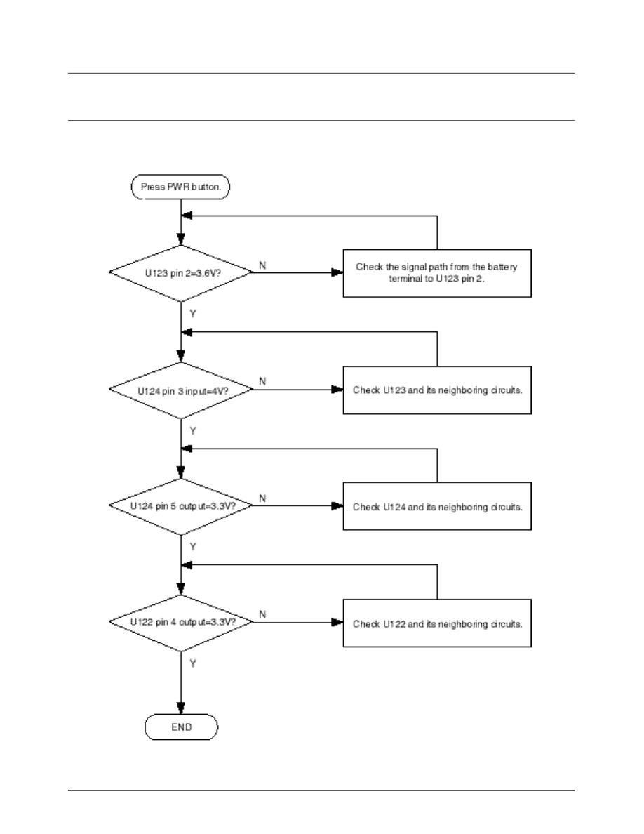
8. Troubleshooting
8-1 Logic Section
8-1-1 No Power
8-2
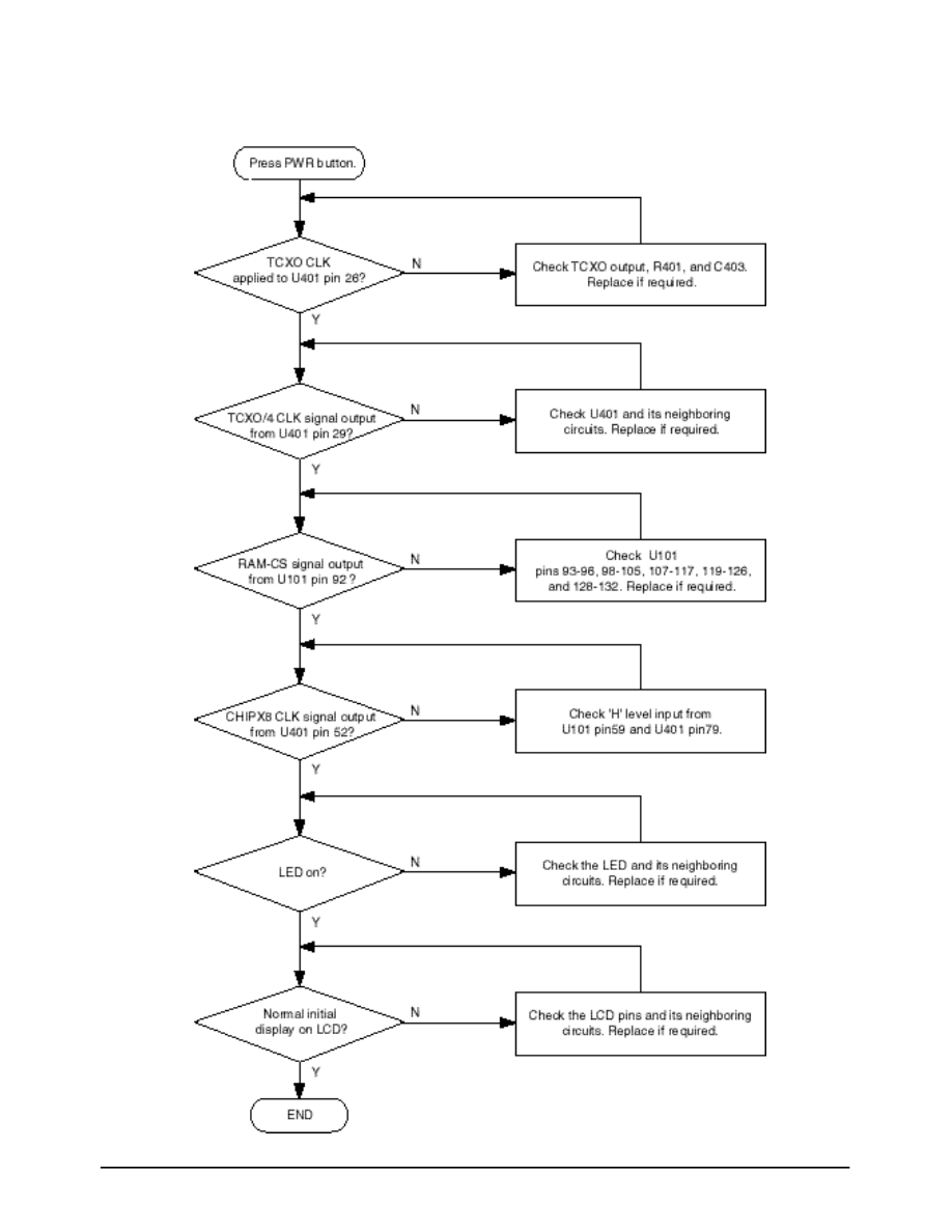
8-1-2 Abnormal Initial Operation
(Normal +3.3V voltage source)
8-3
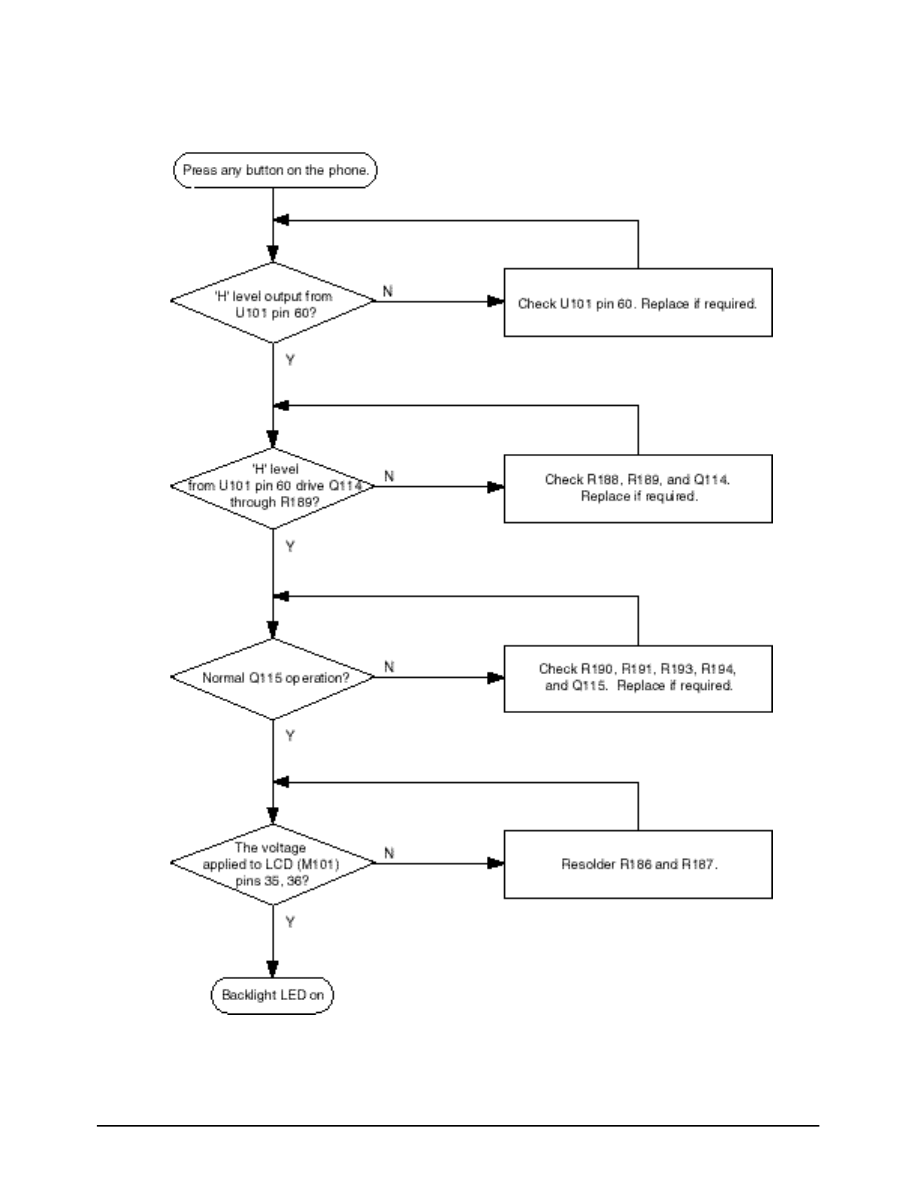
8-1-3 Abnormal Backlight Operation
8-4
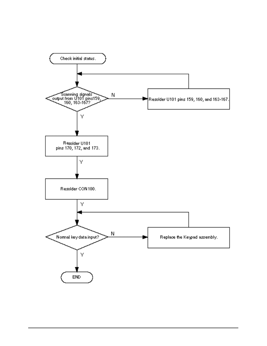
8-1-4 Abnormal Key Data Input
8-5
8-1-5 Abnormal Keytone
8-6
8-1-6 Abnormal Alert Tone
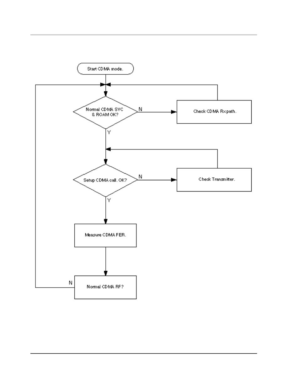
8-7
8-2 RF Section
8-2-1 RF Secton Troubleshooting

8-8
8-2-2 Receiver Part
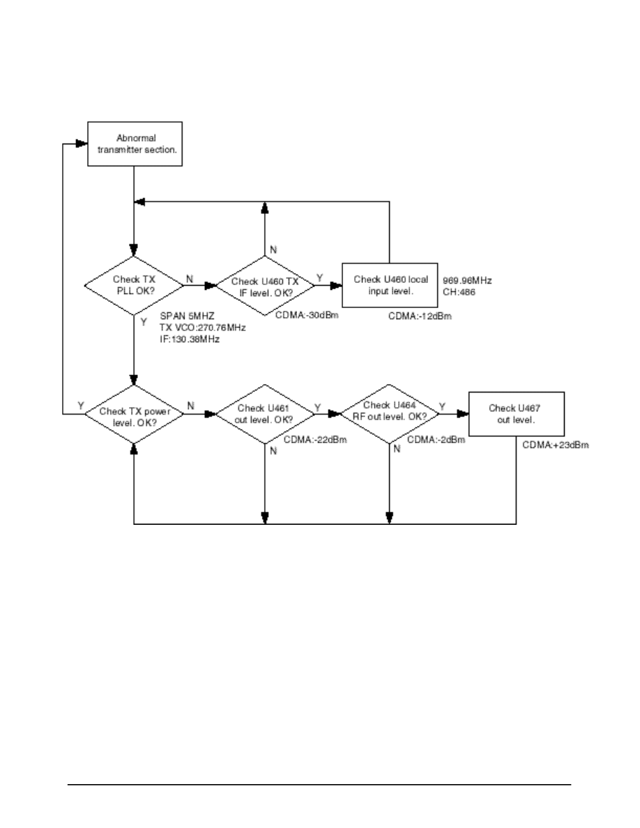
8-9
8-2-3 Transmitter Part
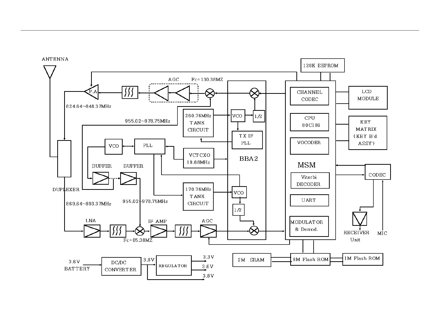
10. Block & Circuit Diagrams
10-1 Block Diagram
Wyszukiwarka
Podobne podstrony:
Samsung SCH A101 service manual
Samsung SCH 8500 service manual
Samsung SCH 880 service manual
Samsung SCH 470 service manual
Samsung SCH A212 service manual
Samsung SCH X359 service manual
Samsung SCH A302 service manual
Samsung SCH 850 service manual
Samsung SCH 6100 service manual
Samsung SCH 870 service manual
Samsung SCH A205 service manual
Samsung SCH A105 service manual
Samsung SGH R200 service manual
Samsung SGH E710 service manual
Samsung SGH T500 service manual
Samsung SGH A408 service manual
Samsung SGH Q208 service manual
Samsung SGH N288 service manual
Samsung SGH A288 service manual
więcej podobnych podstron