– 1 –
SERVICE MANUAL
SPECIFICATIONS
General
Operating channel
25 channels
Dial signal
Tone, 10 PPS (pulse) selectable
Supplied accessories
AC power adaptor (AC-T56) (1) (E92)
AC power adaptor (AC-T124) (1) (E12)
AC power adaptor (AC-T125) (1) (ARGENTINE)
Telephone line cord (1)
Rechargeable battery pack (BP-T16) (1) (SPP-874)
Rechargeable battery pack (BP-T16) (2) (SPP-884)
Wall bracket/stand (1)
Screws (2)
Handset
Power source
Rechargeable battery pack BP-T16
Battery life
Standby : Approx. 14 days
Talk
: Approx. 6 hours
Battery charging time
Approx. 12 hours
Dimensions
Approx. 54
×
195
×
49 mm (w/h/d),
antenna excluded
(approx. 2
1/4
×
7
3/4
×
1
15/16
inches)
Antenna: Approx. 285 mm
(approx. 11
1/4
inches)
Mass
Approx. 240 g (approx. 8 oz), battery
included
SPP-874/884
E Model
CORDLESS TELEPHONE
Base unit
Power source
DC 9V from AC power adaptor
Rechargeable battery pack BP-T16
(SPP-884 only)
Battery charging time
Approx. 20 hours (SPP-884 only)
Dimensions
Approx. 120
×
64
×
223 mm (w/h/d),
antenna excluded
(approx. 4
3/4
×
2
5/8
×
8
7/8
inches)
Antenna: Approx. 680 mm
(approx. 26
7/8
inches)
Mass
Approx. 350 g (approx. 12 oz), wall
bracket and battery excluded
Design and specifications are subject to change without
notice.
• Abbreviation
E12 : 220–240V area of E model
E92 : 120V area of E model
MICROFILM
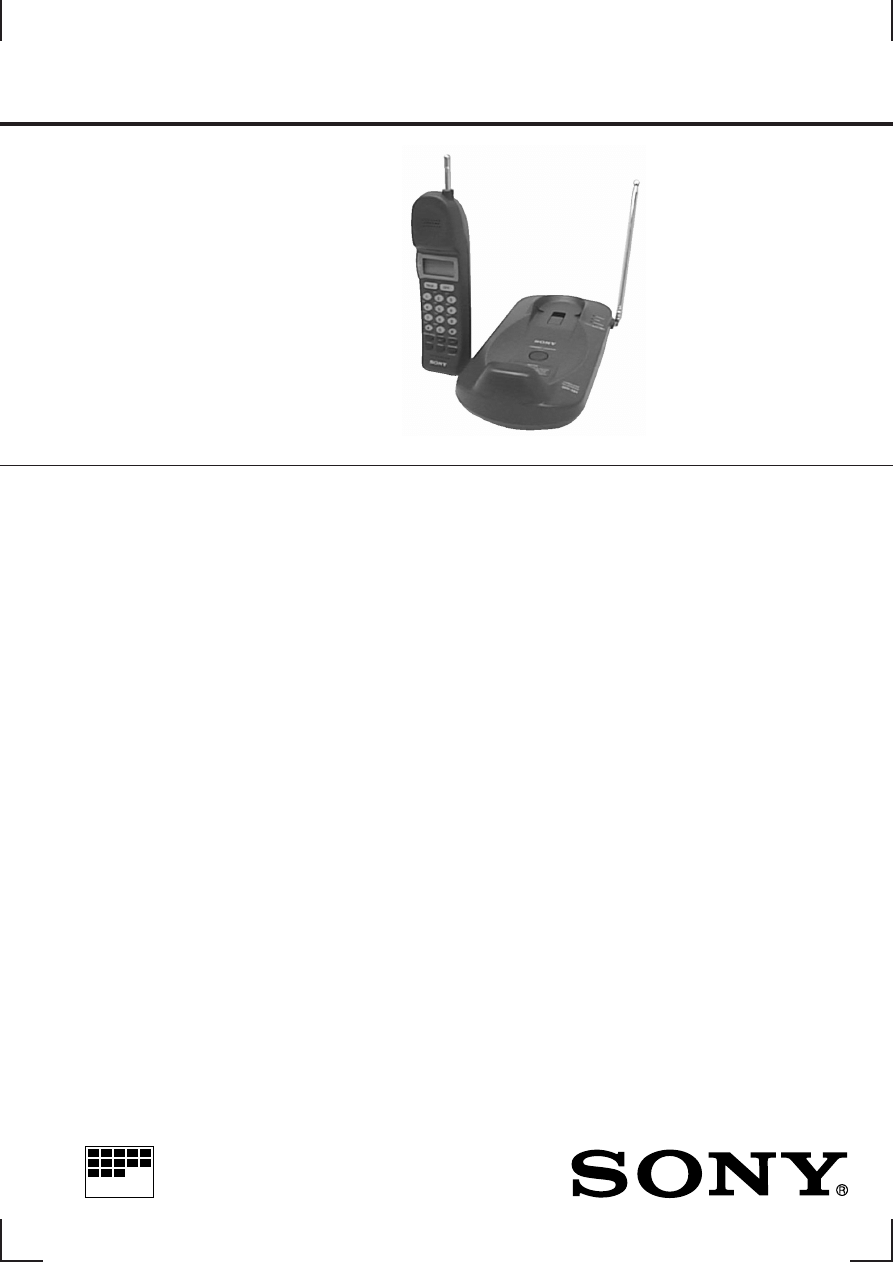
Photo: SPP-884
Handset
Base unit
– 27 –
– 28 –
SPP-874/884
5-4. SCHEMATIC DIAGRAM — BASE SECTION — • Refer to page 37 for IC Block Diagrams.
Note:
• All capacitors are in
µ
F unless otherwise noted.
pF:
µµ
F 50 WV or less are not indicated except for
electrolytics and tantalums.
• All resistors are in
Ω
and
1
/
4
W or less unless other-
wise specified.
•
¢
: internal component.
•
C
: panel designation.
•
U
: B+ Line.
•
H
: adjustment for repair.
• Power voltage is dc 9 V and fed with regulated dc
power supply from external power voltage jack.
• Voltage is dc with respect to ground under
no-signal condition.
• Voltage dc with respect to ground under no-signal
conditions.
• Voltages are taken with a VOM (Input impedance
10 M
Ω
).
Voltage variations may be noted due to normal pro-
duction tolerances.
• Signal path.
N
: RX
O
: TX
P
: bell
• Abbreviation
E12
: 220-240V area of E model
E92
: 120V area of E model
5-6. SCHEMATIC DIAGRAM — HAND MAIN SECTION — • Refer to page 37 for IC Block Diagrams.
– 31 –
– 32 –
SPP-874/884
Note:
• All capacitors are in
µ
F unless otherwise noted. pF:
µµ
F
50 WV or less are not indicated except for electrolytics
and tantalums.
• All resistors are in
Ω
and
1
/
4
W or less unless otherwise
specified.
•
¢
: internal component.
•
U
: B+ Line.
•
H
: adjustment for repair.
• Power voltage is dc 3.6 V and fed with regulated dc power
supply from battery connector (CN2).
• Voltage is dc with respect to ground under no-signal
condition.
• Voltages are taken with a VOM (Input impedance 10 M
Ω
).
Voltage variations may be noted due to normal produc-
tion tolerances.
• Signal path.
N
: RX
O
: TX
• Abbreviation
E12
: 220-240V area of E model
E92
: 120V area of E model
(Page 36)
5-8. SCHEMATIC DIAGRAM — HAND KEY SECTION — • Refer to page 37 for IC Block Diagrams.
– 35 –
– 36 –
SPP-874/884
Note:
• All capacitors are in
µ
F unless otherwise noted. pF:
µµ
F
50 WV or less are not indicated except for electrolytics
and tantalums.
•
C
: panel designation.
•
U
: B+ Line.
• Power voltage is dc 3.6 V and fed with regulated dc power
supply from battery connector (CN2).
• Voltage is dc with respect to ground under no-signal
condition.
• Voltages are taken with a VOM (Input impedance 10 M
Ω
).
Voltage variations may be noted due to normal produc-
tion tolerances.
• Abbreviation
E12
: 220-240V area of E model
E92
: 120V area of E model
(Page 32)
• IC Block Diagrams
– 37 –
– 38 –
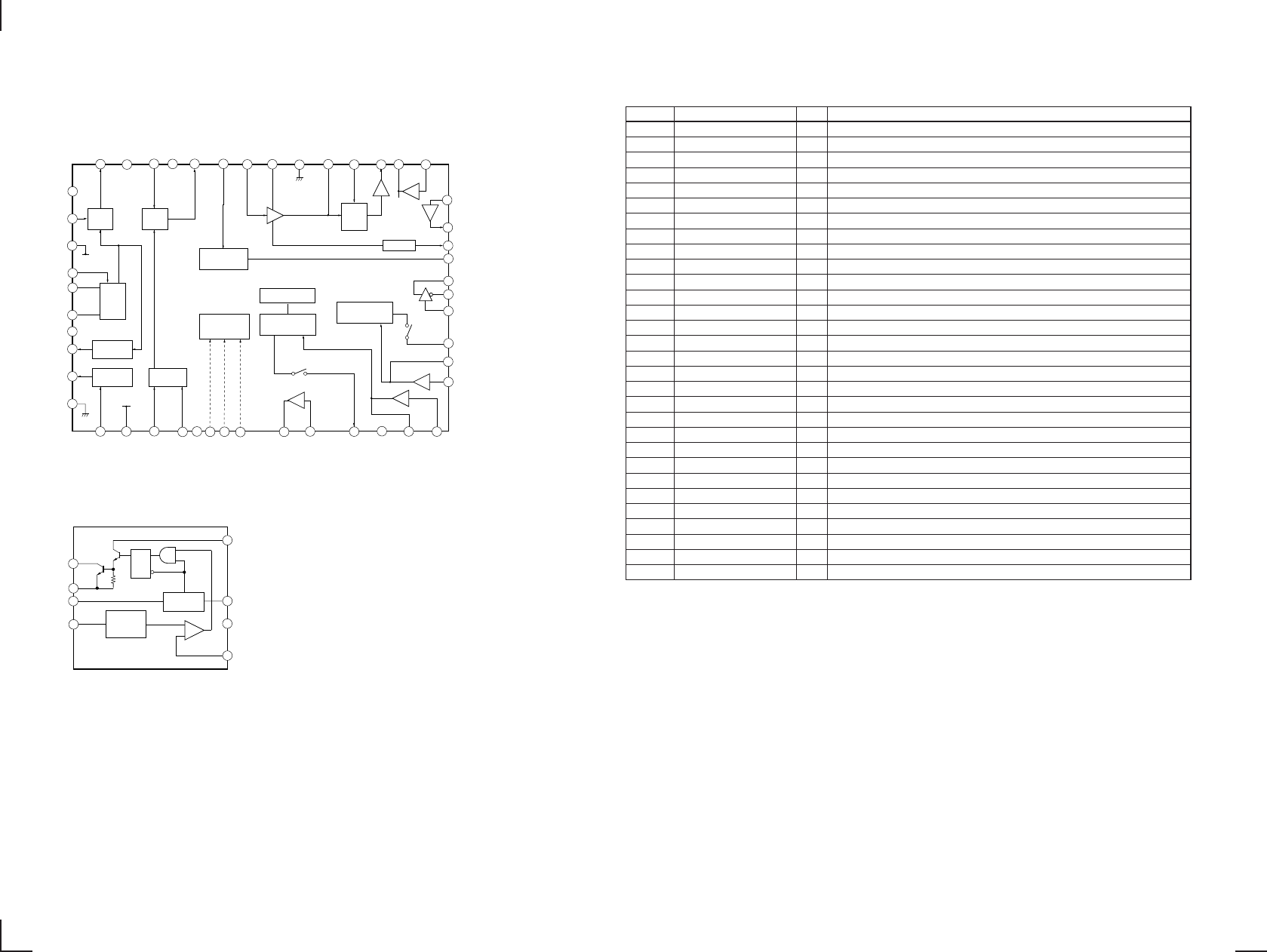
5-9. IC PIN DESCRIPTIONS
• IC801 LC6621108A (SYSTEM CONTROL) (BASE UNIT)
Pin No.
Pin Name
I/O
Pin Description
1
RSSI CTRL
O
RSSI sens select output (L: Low sens)
2
EEPROM DATA
I/O
EEPROM data input/output (Not used in this set.)
3
EEROM CLK
O
EEPROM clock output (Not used in this set.)
4
RX-DATA
I
RF reception data input
5
CHARGE DET
I
Charge detection input
6
TX-DATA
O
Beep output at RF transmission data or outside the circle.
7
HOLD DET
I
Hold cancellation detection input
8
GND
—
Ground
9
OSC1
—
Crystal oscillation input (4.048MHz)
10
OSC2
—
Crystal oscillation output (4.048MHz)
11
VDD
—
Power supply pin
12
RESET
—
Reset input
13
TEST
—
Not used. (Fixed at L in this set.)
14
AC DET
I
AC adaptor without detection input
15
RING DET
I
Ring detection input
16
PLL-STB
O
PLL control standby output
17
PLL-CLK
O
PLL control clock output
18
PLL-DATA
O
PLL control data output
19
SIG-DATA-IN
I
RSSI/LOCK signal input (L:RSSI, H:LOCK)
20
TX+B CTRL
O
TX power control output
21
DTMF
O
DTMF output
22
DP
O
Pulse output
23
COL1
I
MODEL1/PAGE input
24
COL2
I
MODEL2/ T/P input
25
COL3
I
MODEL3/MAKE input
26
COL4
I
FLASH time/ D/P input
27
ROW1
O
Matrix 1 output
28
ROW2
O
Matrix 2 output
29
TEST I/O
I/O
At TEST start-up or ID writing, data input/output. (L: TEST start-up)
30
TEST CLK/POWER LED
I/O
At initial ID writing, clock input/output and flashing on power failure.
IC501
TB31224F (BASE MAIN BOARD)
IC1
TB31224F (HAND MAIN BOARD)
IC901
MC34063AM
39
40
41
42
43
44
45
46
47
48
1
2
3
4
5
6
7
8
9
10
38
37
36
35
34
32
33
31
30
29
28
27
26
25
24
23
22
21
20
19
18
17
16
15
14
13
12
11
1st
MIXER
2nd
MIXER
BATTERY
ALARM
DATA
LATCH
CONTROL
LIMITER
EXPANDER
COMPRESSOR
IF AMP
QUOD
LACHA
DETECT
LPF
NOISE
FILTER
DATA
COMPARATOR
RSSI
RECEIVE
AMP
E-MUTE
C-MUTE
MIC
AMP
PRE AMP
SPLATTER
2nd
LOCAL
TX
PLL
RX
PLL
RX
VCO
VREF
VCC2
C-RECT
VCC3
E-RECT
N-REC
VCC1
GND1
C-NF
8
+
–
1.25V
REFERENCE
REGULATOR
R
CT
Q
S
7
6
5
4
3
COMPARATOR
IPK
OSCILLATOR
2
1
DRIVER
COLLECTOR
COMPARATOR
INVERTING
INPUT
IPK SENSE
VCC
GND
TIMING
CAPACITOR
SWITCHING
EMITTER
SWITCHING
COLLECTOR

– 39 –
• IC401 LC662716A (SYSTEM CONTROL) (HANDSET)
Pin No.
Pin Name
I/O
Pin Description
1
BEEP ATT
O
Beep volume High/Low control output (L: High)
2
TX-DATA
O
RF transmission data output
3
BEEP
O
Beep output
4
VSS
—
Ground
5
OSC1
—
Crystal oscillation input (4.048MHz)
6
OSC2
—
Crystal oscillation output (4.048MHz)
7
VDD
—
Power supply pin
8
RESET
—
Reset input
9
BAT-IN
I
Battery detection input
10
PE1
—
Not used. (Fixed at L in this set.)
11
TEST
—
Not used. (Fixed at L in this set.)
12
HOLD
I
Input for intermittent. (CR external)
13 – 16
ACT4
O
Output for intermittent reception control. (L: at operation)
17
CHARGE DET
I
Charge detection input (H: in charge)
18
BAT-LOW-IN
I
Battery low-voltage detection input
19
—
—
Not used. (Fixed at L (SPP-874/884:E92), H (SPP-884:E12) in this set.)
20
RX-DATA
I
RF reception data input
21
PLL-STB
O
PLL control standby output
22
PLL-DATA
O
PLL control data output
23
PLL-CLK
O
PLL control clock output
24
SIG-DATA-IN
I
RSSI/LOCK signal input (L: RSSI, H: LOCK)
25
TX+B CTRL
O
TX power control output
26
HICUT MUTE
O
High band noise mute output
27
RSSI CTRL
O
RSSI sens select output (L: Low sens)
28
VOLUME
O
VOLUME HIGH/NORM select output
29 – 32
P80 – 83
O
Not used. (Fixed at H in this set.)
33
MODE0
I
Destination model select input 0 (Fixed at L (SPP-874:E92/884),
H (SPP-874:E12) in this set.)
34
MODE1
I
Destination model select input 1 (Fixed at L in this set.)
35
TEST CLK
I/O
At initial ID writing, clock input/output.
36
TEST I/O
I/O
At TEST start-up or ID writing, data input/output. (L: TEST start-up)
37, 38
PA0, 1
—
Not used. (Fixed at L in this set.)
39
LIGHT
O
Key & LCD back light LED control output
40
TALK LED
O
TALK LED control output
41 – 45
ROW1 – 5
O
Key matrix output
46
JOG-EN1
I
JOG input
47
JOG-PUSH
I
JOG input
48
JOG-EN2
I
JOG input
49 – 52
COL1 – 4
I
Key matrix input
53
LCD+B CTRL
O
LCD power control output (L: at operation)
54
LCD-E
O
LCD-R/W trigger output
55
LCD-R/W
O
LCD-R/W control output
56
LCD-RS
O
LCD register select signal output
57 – 60
LCD-DB4 – 7
O
LCD-DATA output
61
EEPROM WP
O
EEPROM write protect output
62
EEPROM DATA
I/O
EEPROM data input/output
63
EEPROM CLK
O
EEPROM clock output
64
MIC ON
O
MIC ON/OFF control output (L: OFF)
Wyszukiwarka
Podobne podstrony:
Leptospira spp
Badanie wpywu komponentw modelu SPP na dokadno wyznaczenia
Podstawy Technik Prac Biurowych, moje prace semestralne, spp
Oznaczanie obecności pałeczek?mpylobacter spp
SPP rok 09 numer 3 Wzory użytkowe i ich ochrona
wykres do spp
884
SPP rok 09 numer 3 Unieważnienie prawa ochronnego
SPP rok 09 numer 3 Względne podstawy odmowy udzielenia prawa ochronnego na znak towarowy
Pseudomonas spp
Clostridium spp
489 Polska reklama 7151 874 4
Zasady funkcjonowania biura w firmie, moje prace semestralne, spp
Schistosoma spp
Salmonella spp konspekt
KRUPS F 874
884
więcej podobnych podstron