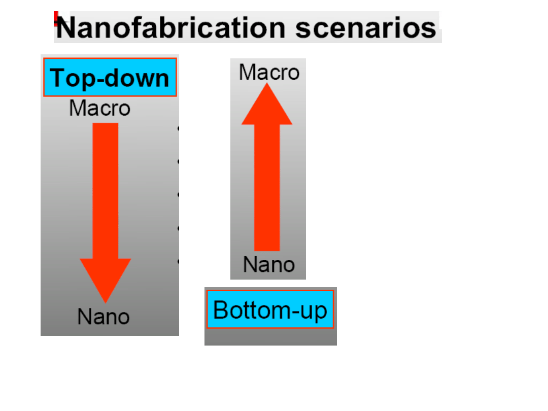
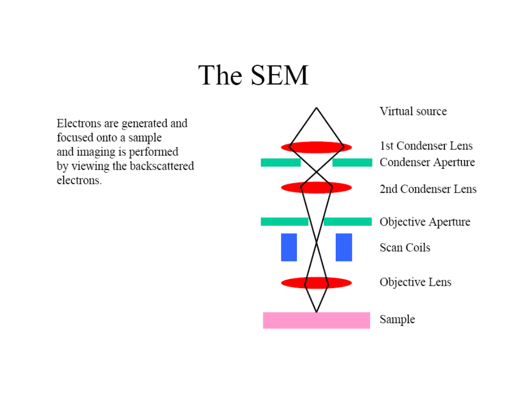
How do we see nanostructures?
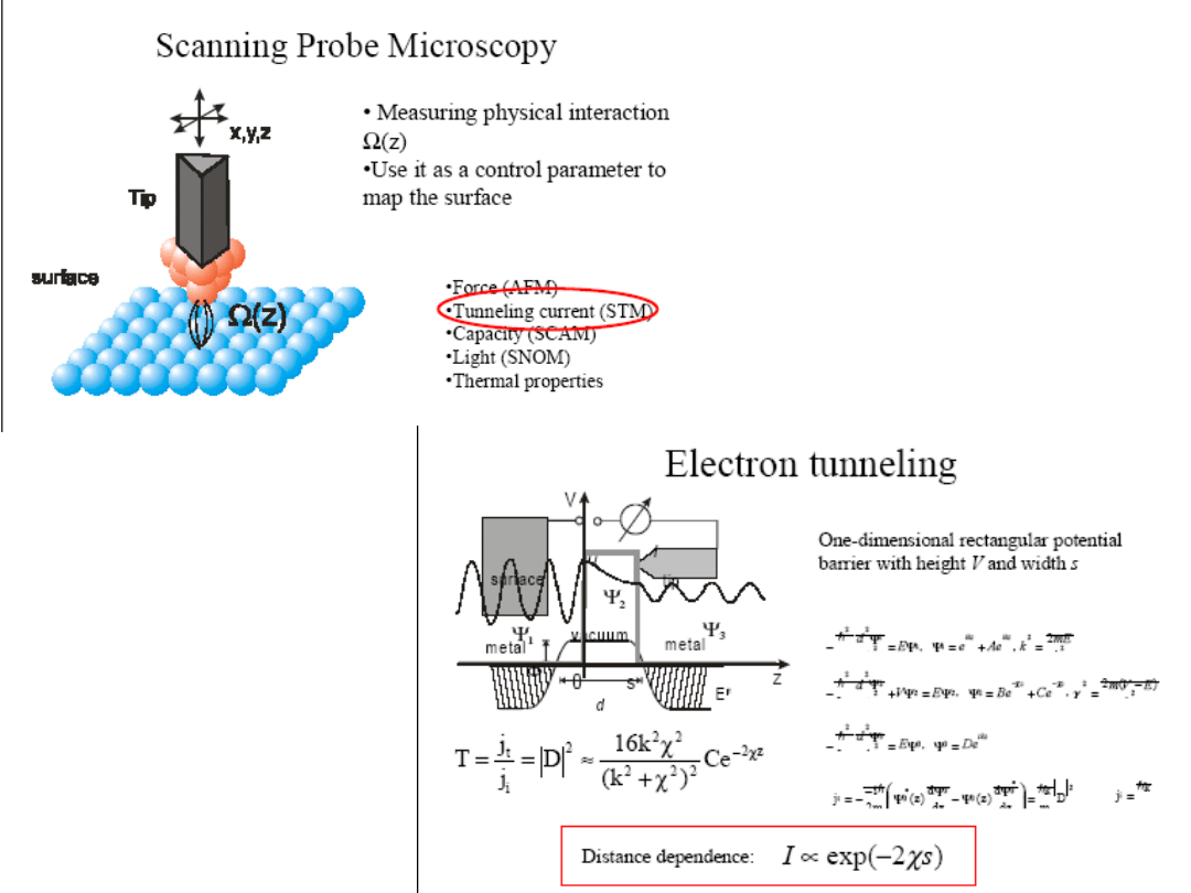
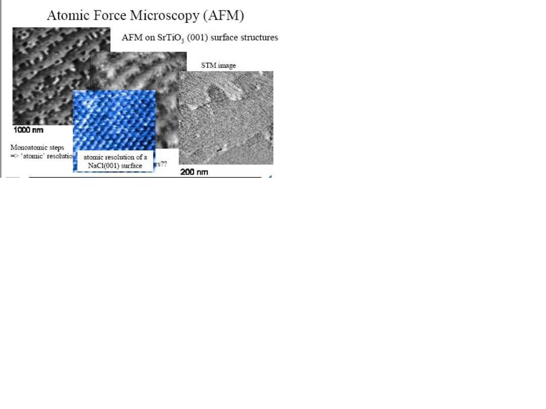
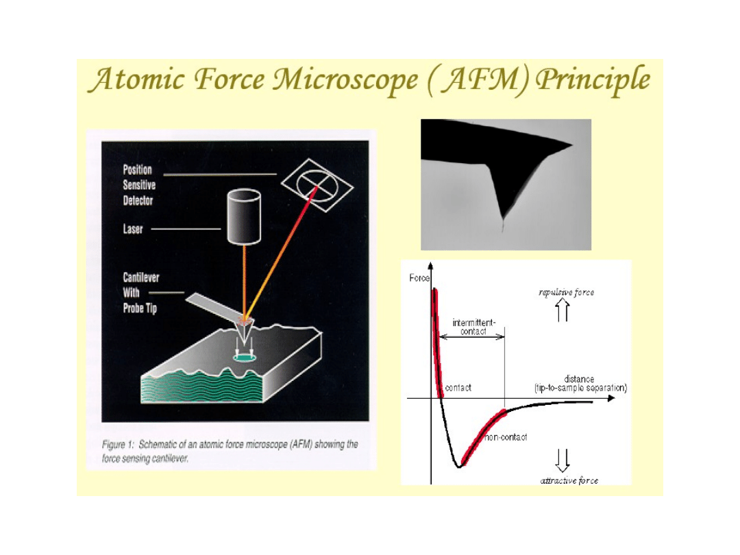
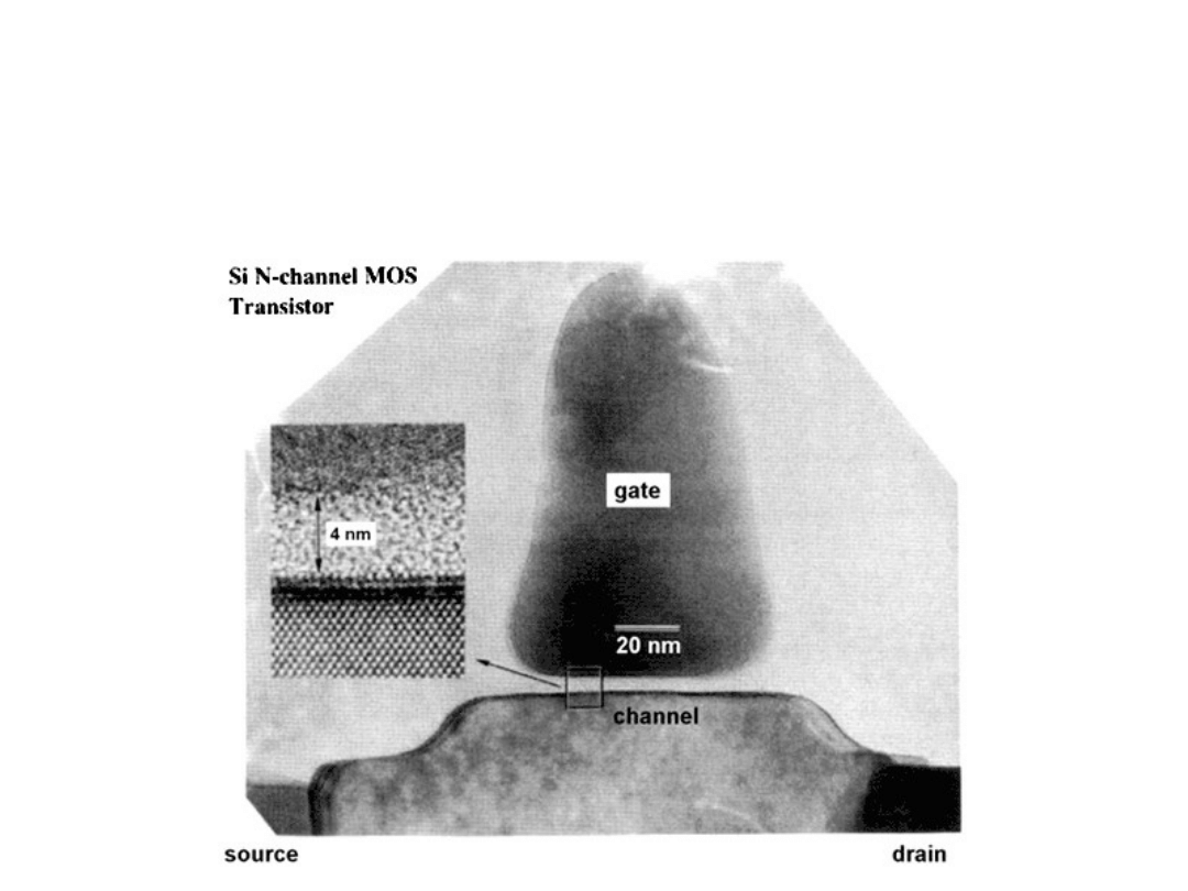
Figure 1.3.2 Electron micrograph of an SiO
2
/Si interface in a
transistor.
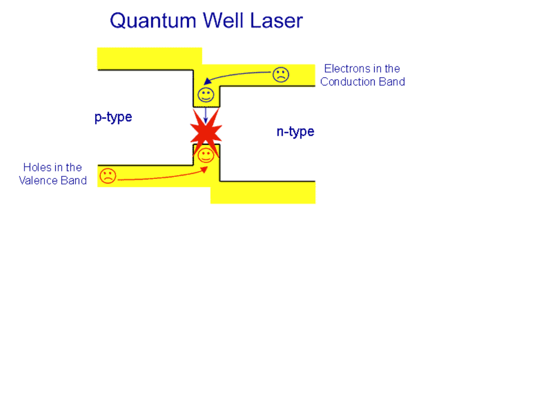
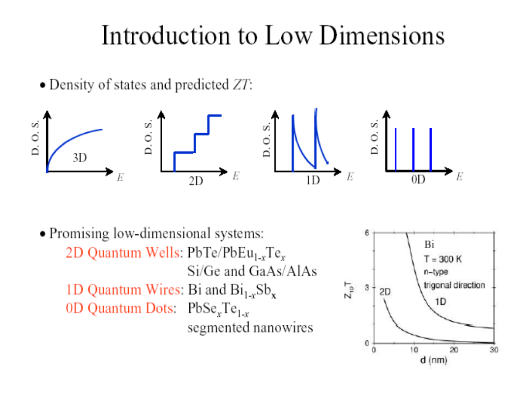
Fig. 1.3.1 Cartoon of the action of a quantum well laser.
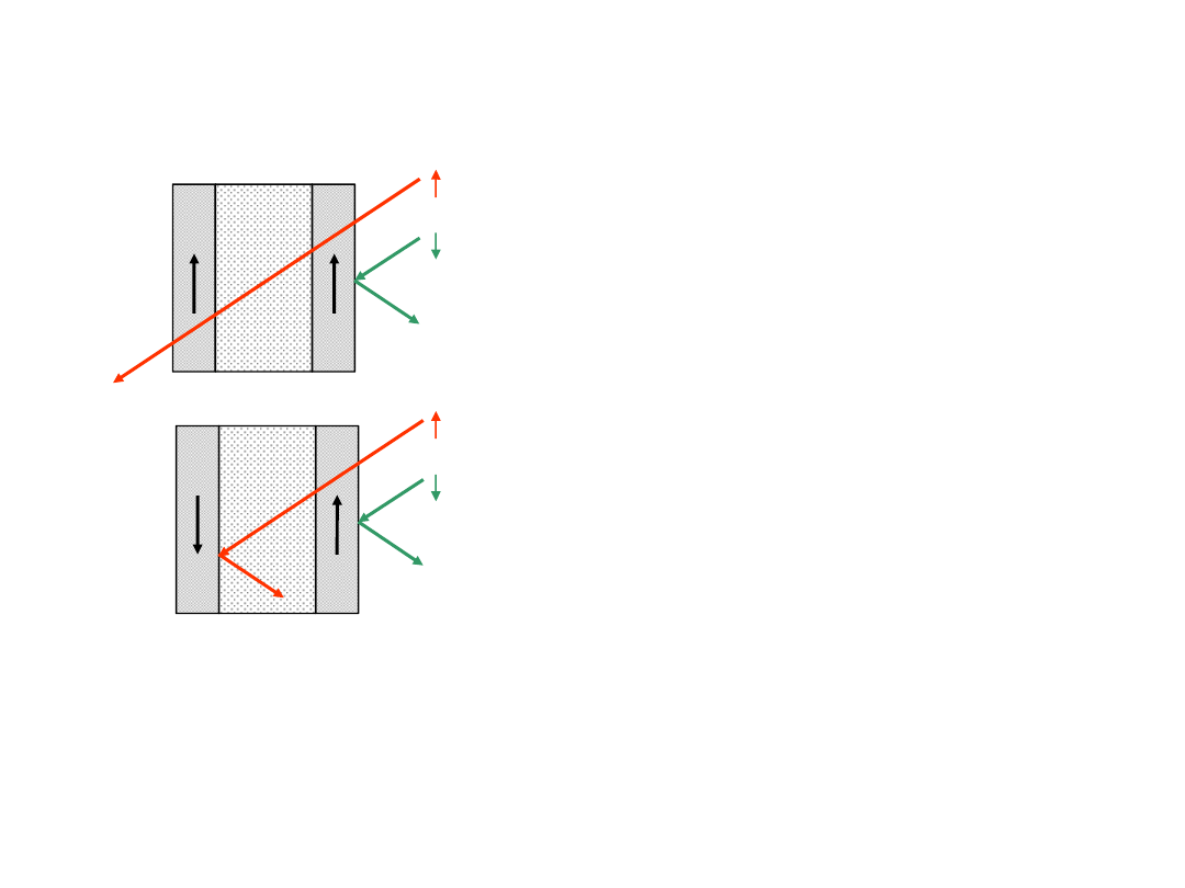
Parallel Spin Filters
→
Resistance Low
Opposing Spin Filters
→
Resistance High
Giant Magnetoresistance (GMR)
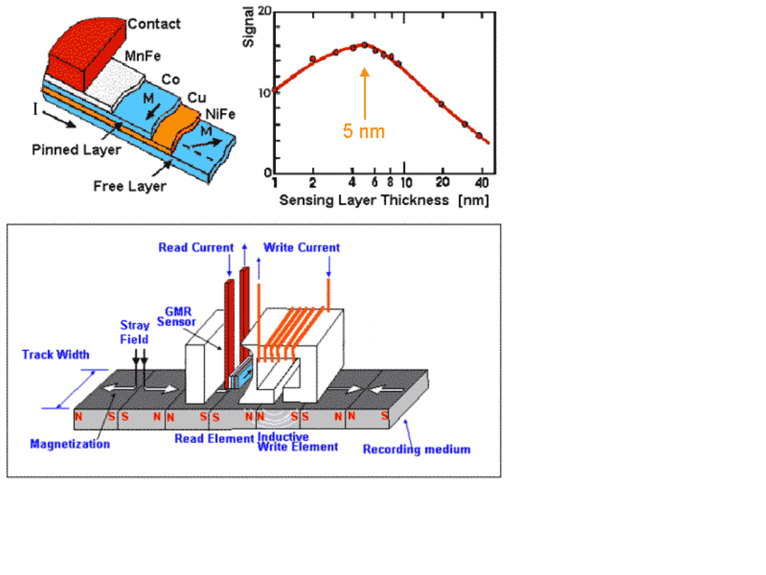
Figure 1.3.3 GMR (giant magnetoresistive) spin valve reading head. At the upper left is a diagram showing how the GMR
phenomenon is used to control current. At the upper right, a graph of signal versus sensing layer thickness shows the optimum
thickness. At the bottom is a diagram showing the interaction of the read/write head and the magnetic storage medium. The GMR
read head is the red block with the read current passing through.
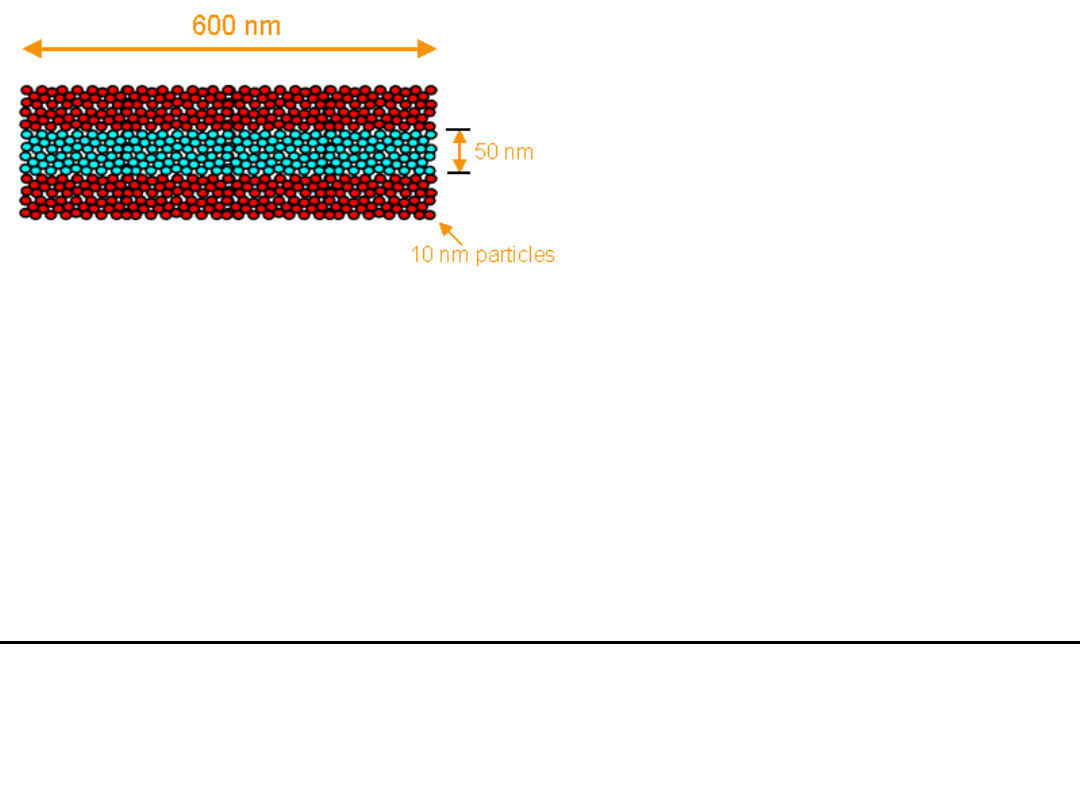
Figure 1.1.2 shows diagrammatically just how much storage density can still be increased. Today's commercial
media can store about 14 Gbits/inch
2
. To achieve this density, the storage medium required to store one bit is a
rectangle of dimensions 600 nm by 50 nm. This is represented by the blue rectangle in the middle of Figure 1.1.2.
Think of the neighboring rectangles as bits that are magnetically oriented in the other direction. One can see how
many 10nm particles are covered by each of the bits, and how much storage density would increase if one can
use one particle to store one biteven without shrinking the size of the particles themselves.
For a good synopsis on how far storage density has already advanced, visit IBM's
page.
Figure 1.1.2 Cartoon showing how much room on a magnetic storage medium is currently needed to store one
bit.
• A photolithography system
consist of a projection
system, a mask, and a
surface coated with a
photo-sensitive film
• The light changes the
properties of the film
locally
• This allows the film to be
partly removed and the
substrate to be selectively
exposed to etching or
deposition
Photo lithography
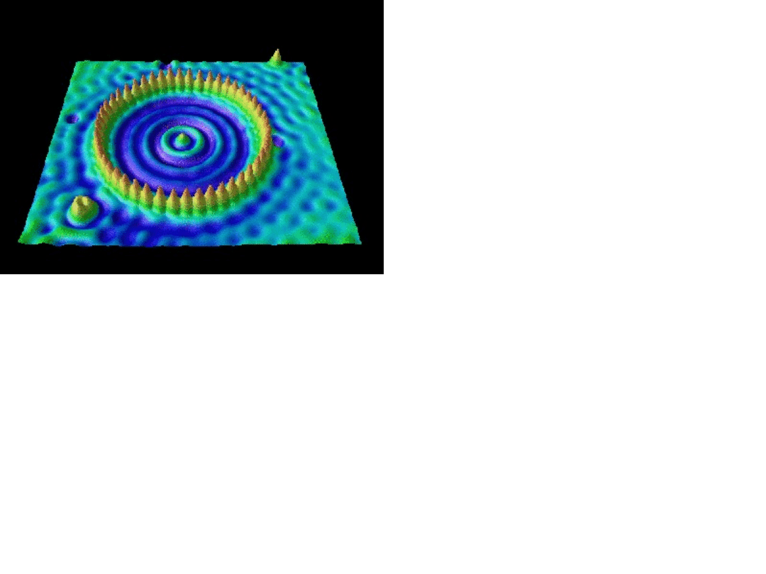
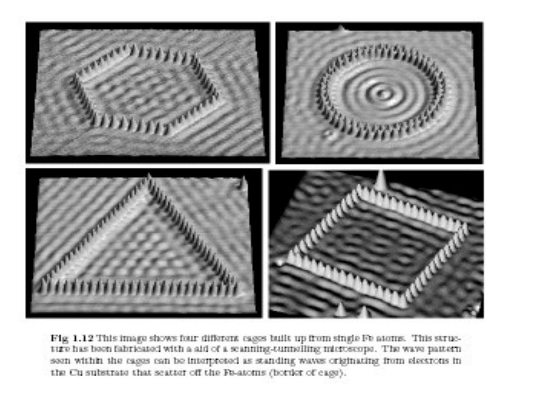
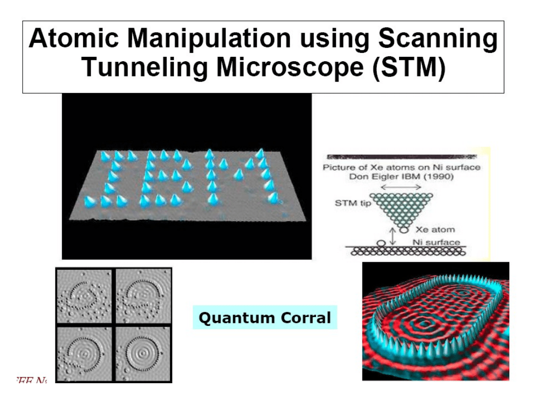
Top: STM image of a
consisting of a ring of iron
atoms assembled on a copper surface. It can be used to
mainpulate the electron wave function. The waves inside the ring
represent direct detection of the electron wave function by STM;
there is no iron atom in the center

•
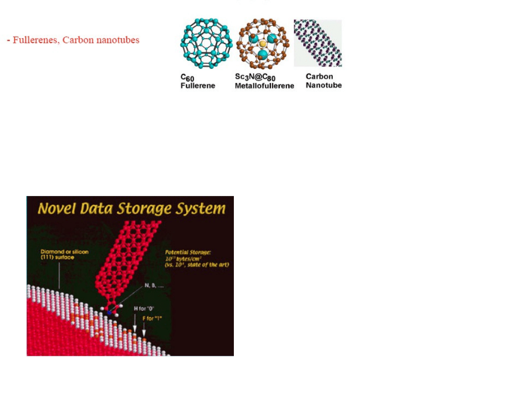
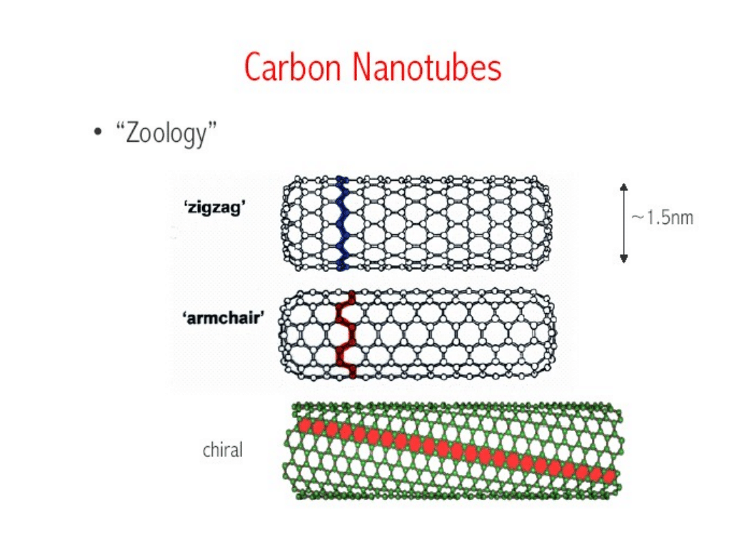
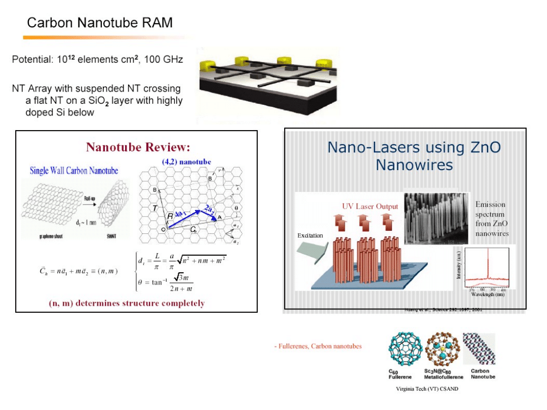
Quick Facts About Carbon Nanotubes
•
Equilibrium Structure
•Average Diameter of SWNT's 1.21.4 nm
•Distance from opposite Carbon Atoms (Line 1) 2.83 Å
•Analogous Carbon Atom Separation (Line 2) 2.456 Å
•Parallel Carbon Bond Separation (Line 3) 2.45 Å
•Carbon Bond Length (Line 4) 1.42 Å
•CC Tight Bonding Overlap Energy ~ 2.5 eV
•Group Symmetry (10, 10) C5V
•Lattice: Bundles of Ropes of Nanotubes: Triangular
Lattice(2D)
•Lattice Constant 17 Å
•Lattice Parameter:
•(10, 10) Armchair 16.78 Å
•(17, 0) Zigzag 16.52 Å
•(12, 6) Chiral 16.52Å
•Density:
•(10, 10) Armchair 1.33 g/cm3
•(17, 0) Zigzag 1.34 g/cm3
•(12, 6) Chiral 1.40 g/cm3
•Interlayer Spacing:
•(n, n) Armchair 3.38 Å
•(n, 0) Zigzag 3.41 Å
•(2n, n) Chiral 3.39 Å
•
Optical Properties
•Fundamental Gap:
•For (n, m); nm is divisible by 3 [Metallic] 0 eV
•For (n, m); nm is not divisible by 3 [Semi
Conducting] ~0.5 eV
•
Electrical Transport
•Conductance Quantization n x (12.9 kW)1
•Resistivity 104 W∙cm
•Maximum Current Density 1013 A/m2
•
Thermal Transport
•Thermal Conductivity(Room Temperature) ~ 2000
W/m•K
•Phonon Mean Free Path ~ 100 nm
•Relaxation Time ~ 1011 s
•
Elastic Behavior
•Young's Modulus (SWNT) ~ 1 TPa
•Young's Modulus (MWNT) 1.28 TPa
•Maximum Tensile Strength ~30 GPa
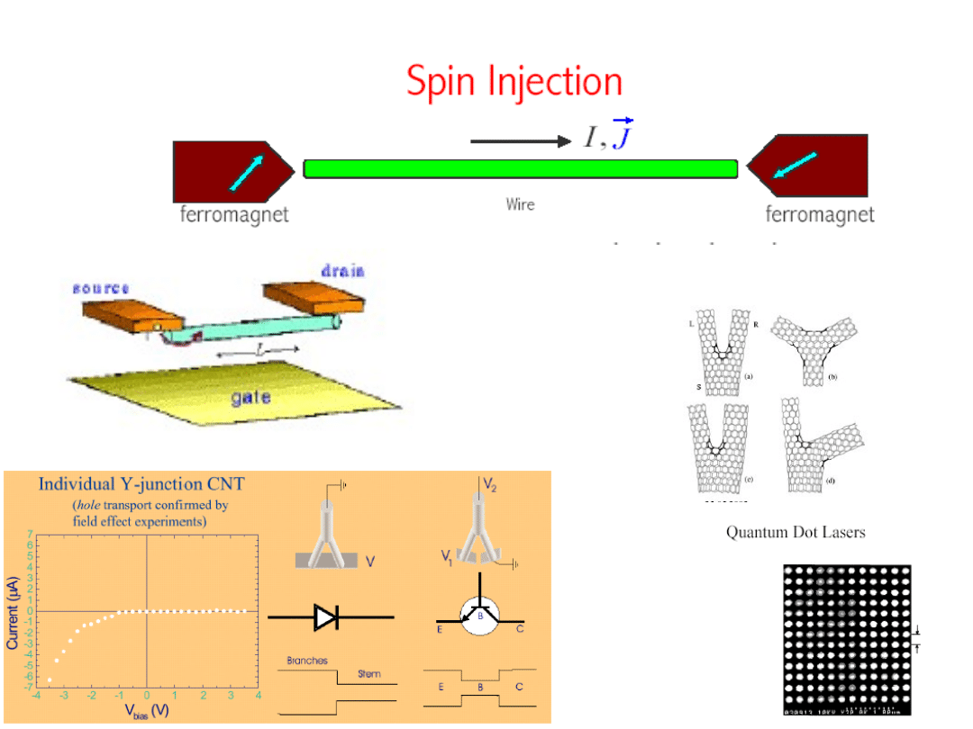
Carbon Nanotube
Field
Emitters
Applications for
Nanotubes
Scanning tips and Electronics
STM/AFM tips
Direct Analysis of DNA
Semiconductor devices
Field Emitters
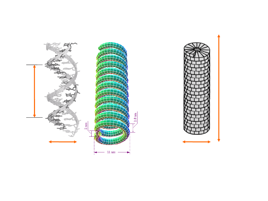
Tobacco Mosaic Virus
(TMV)
DNA
18 nm
300
nm
2 nm
3.4 nm
pitch
10 base
pairs
Document Outline
- Slide 1
- Slide 2
- Slide 3
- Slide 4
- Slide 5
- Slide 6
- Slide 7
- Slide 8
- Slide 9
- Slide 10
- Slide 11
- Slide 12
- Slide 13
- Slide 14
- Slide 15
- Slide 16
- Slide 17
- Slide 18
- Slide 19
- Slide 20
- Slide 21
- Slide 22
- Slide 23
- Slide 24
- Slide 25
- Slide 26
- Slide 27
- Slide 28
- Slide 29
- Slide 30
- Slide 31
- Slide 32
- Slide 33
Wyszukiwarka
Podobne podstrony:
MechKw i14
MechKw i04
MechKw i03
MechKw i05
MechKw i11
I14
MechKw i11
MechKw 03
MechKw 10
MechKw pytania
MechKw i07
lwtm I14
MechKw i12
MechKw 06
MechKw 07
MechKw i13
MechKw i09
MechKw i04
więcej podobnych podstron