VISHAY
MOC8050
Document Number 83659
Rev. 1.4, 20-Apr-04
Vishay Semiconductors
www.vishay.com
1
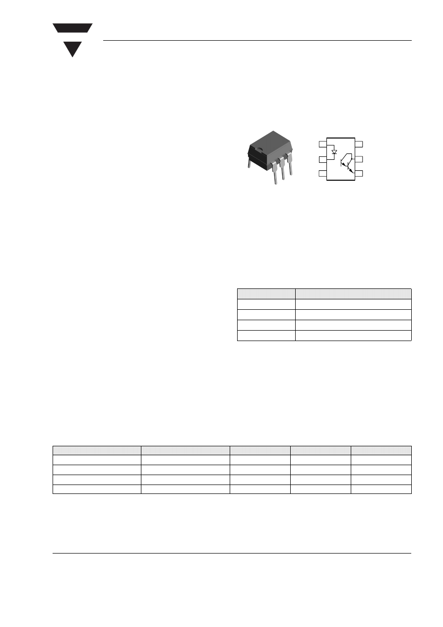
i179013
NC
C
E
A
C
NC
1
2
3
6
5
4
Optocoupler, Photodarlington Output, High Gain
Features
• High Collector to Emitter Breakdown Voltage:
80 V Min
• High Isolation Voltage V
ISO
= 5300 V
RMS
• Base Lead Not Connected
• Solid State Reliability
• Standard DIP Package
Agency Approvals
• UL - File No. E52744 System Code H or J
• DIN EN 60747-5-2(VDE0884)
DIN EN 60747-5-5 pending
Available with Option 1
• CSA 93751
• BSI IEC60950 IEC60965
Applications
Description
The MOC8050 is an optically coupled isolator with a
Gallium Arsenide infrared emitter and a silicon photo-
darlington sensor. Switching can be achieved while
maintaining a high degree of isolation between driving
and load circuits, with no cross talk between chan-
nels. These optocouplers can be used to replace reed
and mercury relays with advantages of long life, high
speed switching and elimination of magnetic fields.
Order Information
For additional information on the available options refer to
Option Information.
Absolute Maximum Ratings
T
amb
= 25 °C, unless otherwise specified
Stresses in excess of the absolute Maximum Ratings can cause permanent damage to the device. Functional operation of the device is
not implied at these or any other conditions in excess of those given in the operational sections of this document. Exposure to absolute
Maximum Rating for extended periods of the time can adversely affect reliability.
Input
Part
Remarks
MOC8050
CTR > 500 %, DIP-6
MOC8050-X006
CTR > 500 %, DIP-6 400 mil (option 6)
MOC8050-X007
CTR > 500 %, SMD-6 (option 7)
MOC8050-X009
CTR > 500 %, SMD-6 (option 9)
Parameter
Test condition
Symbol
Value
Unit
Peak reverse voltage
V
R
3.0
V
Continuous forward current
I
R
60
mA
Power dissipation
P
diss
100
mW
Derate linearly from 25 °C
1.33
mW/°C
www.vishay.com
2
Document Number 83659
Rev. 1.4, 20-Apr-04
VISHAY
MOC8050
Vishay Semiconductors
Output
Coupler
Electrical Characteristics
T
amb
= 25 °C, unless otherwise specified
Minimum and maximum values are testing requirements. Typical values are characteristics of the device and are the result of engineering
evaluation. Typical values are for information only and are not part of the testing requirements.
Input
Output
Coupler
Parameter
Test condition
Symbol
Value
Unit
Collector-emitter breakdown
voltage
BV
CEO
80
V
Collector load current
125
mA
Power dissipation
P
diss
150
mW
Derate linearly from 25 °C
2.0
mW/°C
Parameter
Test condition
Symbol
Value
Unit
Total package dissipation
P
tot
250
mW
Derate linearly from 25 °C
3.3
mW/°C
Isolation test voltage
V
ISO
5300
V
RMS
Isolation resistance
V
IO
= 500 V, T
amb
= 25 °C
R
IO
10
12
Ω
V
IO
= 500 V, T
amb
= 100 °C
R
IO
10
11
Ω
Creepage path
≥ 7
mm
Clearance path
≥ 7
mm
Comparative tracking index
175
Storage temperature range
T
stg
- 55 to +125
°C
Operating temperature range
T
amb
- 55 to +100
°C
Lead soldering time at 260 °C
10
sec.
Parameter
Test condition
Symbol
Min
Typ.
Max
Unit
Forward voltage
I
F
= 20 mA
V
F
1.25
1.5
V
Reverse current
V
R
= 3.0 V
I
R
0.1
10
µA
Capacitance
V
R
= 0
C
O
25
pF
Parameter
Test condition
Symbol
Min
Typ.
Max
Unit
Collector-emitter breakdown
voltage
I
C
= 10
µA
BV
CEO
80
V
Collector-emitter leakage
current
V
CE
= 60 V, I
F
= 0
I
CEO
25
1000
nA
Emitter-collector breakdown
voltage
I
C
= 10
µA
V
ECO
5.0
8.0
V
Parameter
Test condition
Symbol
Min
Typ.
Max
Unit
Collector-emitter saturation
voltage
I
C
= 50 mA, I
F
= 50 mA
V
CEsat
0.9
1.0
V
Isolation test voltage
1.0 s, 60 Hz
V
ISO
5300
V
RMS
Capacitance (input-output)
C
IO
0.5
pF
VISHAY
MOC8050
Document Number 83659
Rev. 1.4, 20-Apr-04
Vishay Semiconductors
www.vishay.com
3
Current Transfer Ratio
Switching Characteristics
Typical Characteristics
(T
amb
= 25
°C unless otherwise specified)
Parameter
Test condition
Symbol
Min
Typ.
Max
Unit
Current Transfer Ratio
I
F
= 10 mA, V
CE
= 1.5 V
CTR
500
%
Parameter
Test condition
Symbol
Min
Typ.
Max
Unit
Rise time
V
CC
= 13.5 V, I
F
= 50 mA,
R
L
= 100
Ω
t
r
10
µs
Fall time
V
CC
= 13.5 V, I
F
= 50 mA,
R
L
= 100
Ω
t
f
35
µs
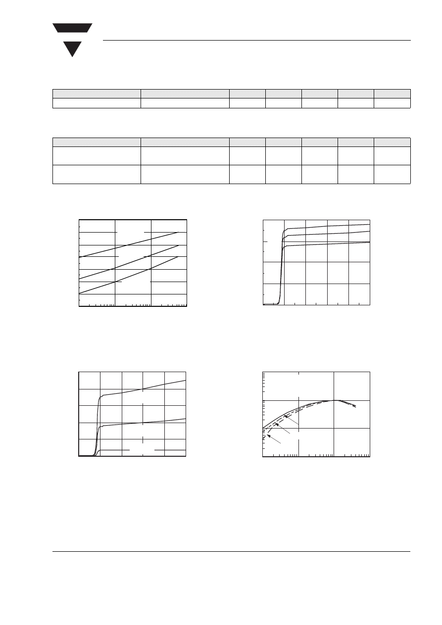
Fig. 1 Forward Voltage vs. Forward Current
Fig. 2 Typical I
C
vs. V
CE
imo c8050_01
IF - Forward Current - mA
100
10
1
.1
0.7
0.8
0.9
1.0
1.1
1.2
1. 3
1.4
VF
-
F
orward
Voltage
-
V
Ta = –55 °C
Ta = 25 °C
Ta = 85 °C
imoc8050_02
5
4
3
2
1
0
0
20
40
60
80
100
VCE - Collector to Emitter Voltage
I C
-
C
ollector
Current
IF=5 mA
IF=1 mA
IF=10 mA
Fig. 3 Typical I
C
vs. V
CE
vs. Temperature
Fig. 4 Typical NCTR vs. LED Current
imoc8050_03
5
4
3
2
1
0
0
2
4
6
8
VCE Collector-Emitter Voltage
I C
-
Collector
Current
25 °C
50 °C
75 °C
imoc8050_04
.1
1
10
100
10
1
.1
.01
IF in mA
NCTR
75 °C
25 °C
50 °C
Normalized @ 25 °C
VCE = 5 V, IF = 10 mA
www.vishay.com
4
Document Number 83659
Rev. 1.4, 20-Apr-04
VISHAY
MOC8050
Vishay Semiconductors
Fig. 5 Typical I
C
vs. V
CE (sat region)
Fig. 6 Typical I
CEO
vs. Temperature
Fig. 7 Low to High Propagation Delay vs. Collector Load
Resistance and LED Current
imoc8050_05
1. 2
1.0
0. 8
0. 6
0. 4
0. 2
0. 0
.01
.1
1
10
100
VCE - Collector to Emitter Voltage
I C
-
Collector
Current
IF=10 mA
IF=5 mA
IF=1 mA
imoc8050_06
80
70
60
50
40
30
20
.1
1
10
100
1000
10000
Temperature in °C
Iceo
in
nA
imoc8050_07
0
5
10
15
20
0
20
40
60
80
VCC = 5 V
Vth = 1,5 V
220
Ω
470
Ω
1K
Ω
IF - LED Current - mA
t pLH
-
Low/High
Propagation
Delay
-
µ
s
100
Ω
Fig. 8 High to low Propagation Delay vs. Collector Load
Resistance and LED Current
Fig. 9 Switching Waveform
Fig. 10 Switching Schematic
imoc8050_08
0
5
10
15
20
0
5
10
15
20
100
Ω
1 k
Ω
IF - LED Current - mA
VCC = 5 V
Vth = 1.5 V
tpHL
-Low/High
Propagation
Delay
-
µ
s
imoc8050_09
I
F
t
R
=1.5 V
V
O
t
D
t
S
t
F
t
PHL
t
PLH
V
TH
imoc8050_10
INPUT
V
OUT
V
CC
= 5 V
R
L
VISHAY
MOC8050
Document Number 83659
Rev. 1.4, 20-Apr-04
Vishay Semiconductors
www.vishay.com
5
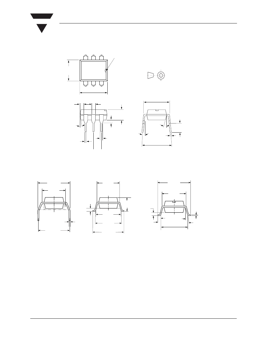
Package Dimensions in Inches (mm)
i178004
.010 (.25)
typ.
.114 (2.90)
.130 (3.0)
.130 (3.30)
.150 (3.81)
.031 (0.80) min.
.300 (7.62)
typ.
.031 (0.80)
.035 (0.90)
.100 (2.54) typ.
.039
(1.00)
Min.
.018 (0.45)
.022 (0.55)
.048 (0.45)
.022 (0.55)
.248 (6.30)
.256 (6.50)
.335 (8.50)
.343 (8.70)
pin one ID
6
5
4
1
2
3
18°
3°–9°
.300–.347
(7.62–8.81)
4°
typ.
ISO Method A
min.
.315 (8.00)
.020 (.51)
.040 (1.02)
.300 (7.62)
ref.
.375 (9.53)
.395 (10.03)
.012 (.30) typ.
.0040 (.102)
.0098 (.249)
15° max.
Option 9
.014 (0.35)
.010 (0.25)
.400 (10.16)
.430 (10.92)
.307 (7.8)
.291 (7.4)
.407 (10.36)
.391 (9.96)
Option 6
.315 (8.0)
MIN.
.300 (7.62)
TYP.
.180 (4.6)
.160 (4.1)
.331 (8.4)
MIN.
.406 (10.3)
MAX.
.028 (0.7)
MIN.
Option 7
18450

www.vishay.com
6
Document Number 83659
Rev. 1.4, 20-Apr-04
VISHAY
MOC8050
Vishay Semiconductors
Ozone Depleting Substances Policy Statement
It is the policy of Vishay Semiconductor GmbH to
1. Meet all present and future national and international statutory requirements.
2. Regularly and continuously improve the performance of our products, processes, distribution and
operatingsystems with respect to their impact on the health and safety of our employees and the public, as
well as their impact on the environment.
It is particular concern to control or eliminate releases of those substances into the atmosphere which are
known as ozone depleting substances (ODSs).
The Montreal Protocol (1987) and its London Amendments (1990) intend to severely restrict the use of ODSs
and forbid their use within the next ten years. Various national and international initiatives are pressing for an
earlier ban on these substances.
Vishay Semiconductor GmbH has been able to use its policy of continuous improvements to eliminate the
use of ODSs listed in the following documents.
1. Annex A, B and list of transitional substances of the Montreal Protocol and the London Amendments
respectively
2. Class I and II ozone depleting substances in the Clean Air Act Amendments of 1990 by the Environmental
Protection Agency (EPA) in the USA
3. Council Decision 88/540/EEC and 91/690/EEC Annex A, B and C (transitional substances) respectively.
Vishay Semiconductor GmbH can certify that our semiconductors are not manufactured with ozone depleting
substances and do not contain such substances.
We reserve the right to make changes to improve technical design
and may do so without further notice.
Parameters can vary in different applications. All operating parameters must be validated for each
customer application by the customer. Should the buyer use Vishay Semiconductors products for any
unintended or unauthorized application, the buyer shall indemnify Vishay Semiconductors against all
claims, costs, damages, and expenses, arising out of, directly or indirectly, any claim of personal
damage, injury or death associated with such unintended or unauthorized use.
Vishay Semiconductor GmbH, P.O.B. 3535, D-74025 Heilbronn, Germany
Telephone: 49 (0)7131 67 2831, Fax number: 49 (0)7131 67 2423
Document Outline
Wyszukiwarka
Podobne podstrony:
BYV27 50 BYV27 200 (Vishay)
BF970 Vishay elenota pl
BF966S (Vishay)
BZX79 x2V4 x75 (Vishay)
SFH628A, SFH6286 (Vishay)
Si3430DV (Vishay)
XT26T (Vishay)
SUP40N25 60 (Vishay)
Vishay LTO 50
SFH615A, SFH6156 (Vishay)
BPW96 (Vishay)
MOC8030, MOC8050 (Motorola)
XT49M (Vishay)
SFH617A [Vishay]
SUB65P06 20, SUP65P06 20 (Vishay)
TCZT8020 (Vishay)
SFH618x (Vishay)
XO 523 (Vishay)
więcej podobnych podstron