BPW96
Vishay Telefunken
1 (6)
Rev. 3, 16-Nov-99
www.vishay.de
•
FaxBack +1-408-970-5600
Document Number 81532
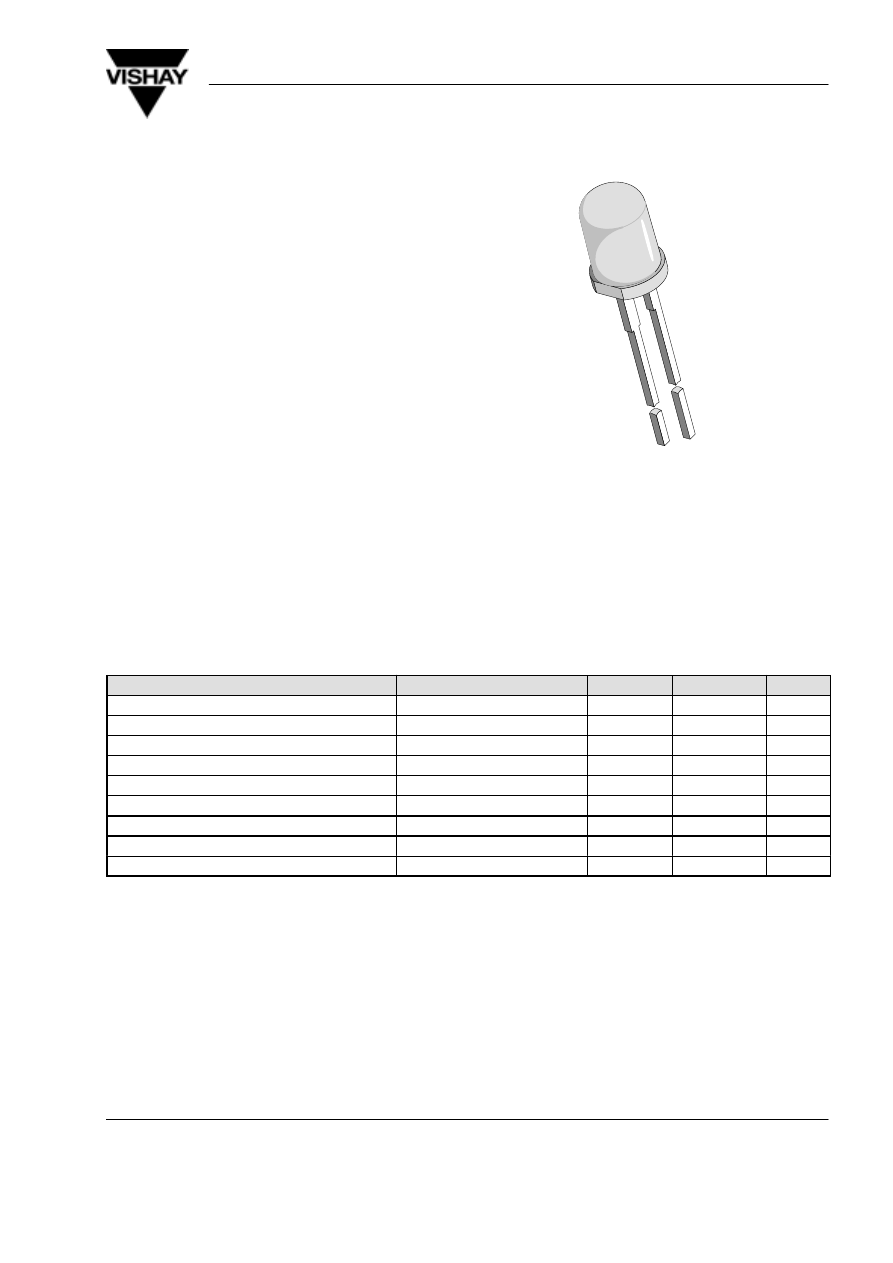
Silicon NPN Phototransistor
Description
BPW96 is a high speed and high sensitive silicon NPN
epitaxial planar phototransistor in a standard T–1
¾
(ø 5 mm) package. Due to its waterclear epoxy the de-
vice is sensitive to visible and near infrared radiation.
The viewing angle of
±
20
°
makes it insensible to ambi-
ent straylight.
Features
D
Fast response times
D
High photo sensitivity
D
Standard T–1
¾
(ø 5 mm) clear plastic package
D
Angle of half sensitivity
ϕ
=
±
20
°
D
Suitable for visible and near infrared radiation
D
Selected into sensitivity groups
94 8391
Applications
Detector in electronic control and drive circuits
Absolute Maximum Ratings
T
amb
= 25
_
C
Parameter
Test Conditions
Symbol
Value
Unit
Collector Emitter Voltage
V
CEO
70
V
Emitter Collector Voltage
V
ECO
5
V
Collector Current
I
C
50
mA
Peak Collector Current
t
p
/T = 0.5, t
p
x
10 ms
I
CM
100
mA
Total Power Dissipation
T
amb
x
47
°
C
P
tot
150
mW
Junction Temperature
T
j
100
°
C
Storage Temperature Range
T
stg
–55...+100
°
C
Soldering Temperature
t
x
3 s
T
sd
260
°
C
Thermal Resistance Junction/Ambient
R
thJA
350
K/W
BPW96
Vishay Telefunken
2 (6)
Rev. 3, 16-Nov-99
www.vishay.de
•
FaxBack +1-408-970-5600
Document Number 81532
Basic Characteristics
T
amb
= 25
_
C
Parameter
Test Conditions
Symbol
Min
Typ
Max
Unit
Collector Emitter Breakdown
Voltage
I
C
= 1 mA
V
(BR)CE
O
70
V
Collector Dark Current
V
CE
= 20 V, E = 0
I
CEO
1
200
nA
Collector Emitter Capacitance
V
CE
= 5 V, f = 1 MHz, E = 0
C
CEO
3
pF
Angle of Half Sensitivity
ϕ
±
20
deg
Wavelength of Peak Sensitivity
l
p
850
nm
Range of Spectral Bandwidth
l
0.5
620...980
nm
Collector Emitter Saturation
Voltage
E
e
= 1 mW/cm
2
,
l
= 950 nm, I
C
= 0.1 mA
V
CEsat
0.3
V
Turn–On Time
V
S
= 5 V, I
C
= 5 mA,
R
L
= 100
W
t
on
2.0
m
s
Turn–Off Time
V
S
= 5 V, I
C
= 5 mA,
R
L
= 100
W
t
off
2.3
m
s
Cut–Off Frequency
V
S
= 5 V, I
C
= 5 mA,
R
L
= 100
W
f
c
180
kHz
Type Dedicated Characteristics
T
amb
= 25
_
C
Parameter
Test Conditions
Type
Symbol
Min
Typ
Max
Unit
Collector Light Current E
e
=1mW/cm
2
,
BPW96A
I
ca
1.5
2.5
4.5
mA
g
e
l
=950nm, V
CE
=5V
BPW96B
I
ca
2.5
4.5
7.5
mA
BPW96C
I
ca
4.5
8
15
mA
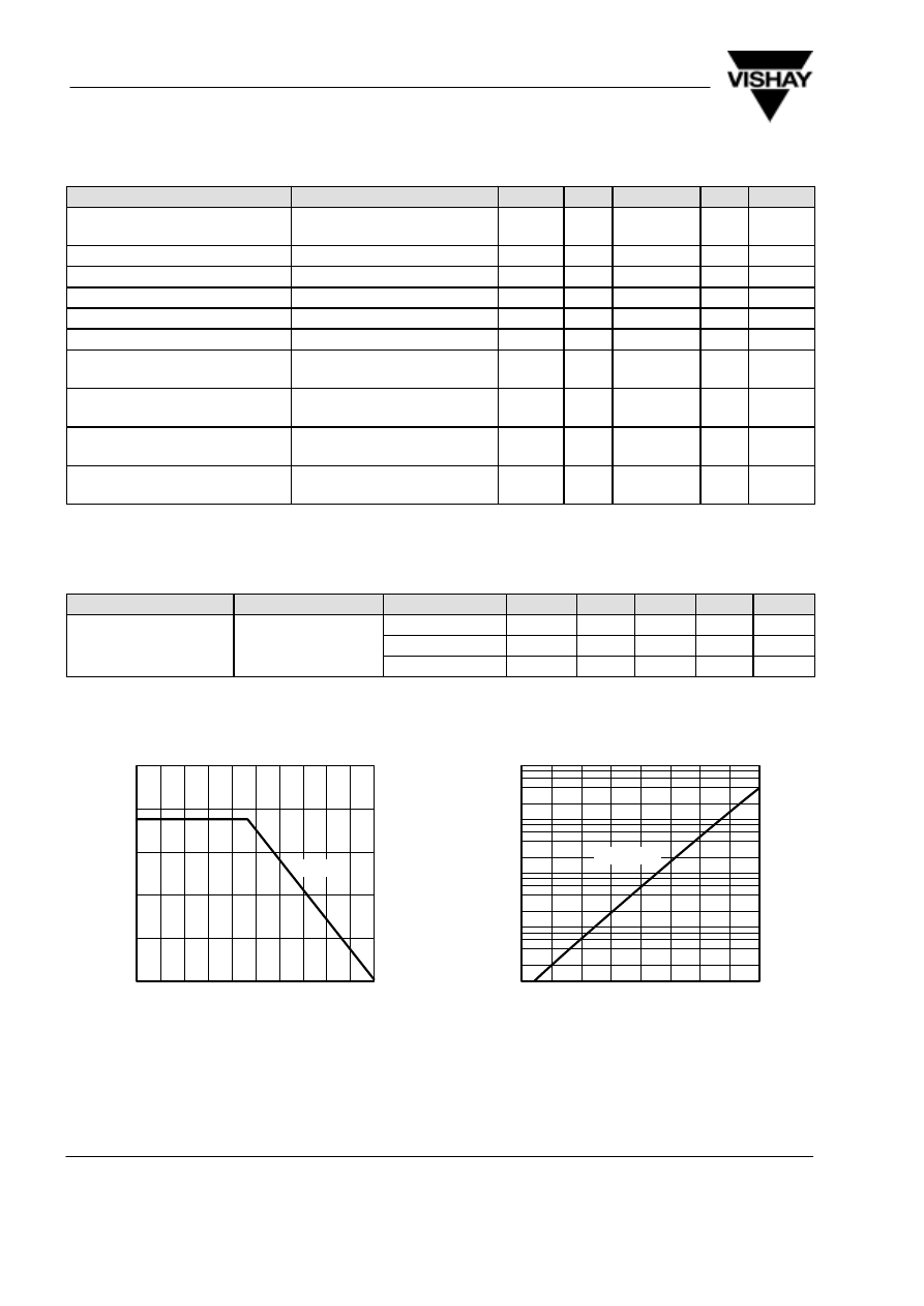
Typical Characteristics (T
amb
= 25
_
C unless otherwise specified)
0
20
40
60
80
0
40
80
120
160
200
P
–
T
otal Power Dissipation ( mW
)
tot
T
amb
– Ambient Temperature (
°
C )
100
94 8300
R
thJA
Figure 1. Total Power Dissipation vs.
Ambient Temperature
94 8304
20
I – Collector Dark Current ( nA
)
CEO
100
40
60
80
T
amb
– Ambient Temperature (
°
C )
10
0
10
1
10
2
10
3
10
4
V
CE
=20V
Figure 2. Collector Dark Current vs. Ambient Temperature
BPW96
Vishay Telefunken
3 (6)
Rev. 3, 16-Nov-99
www.vishay.de
•
FaxBack +1-408-970-5600
Document Number 81532
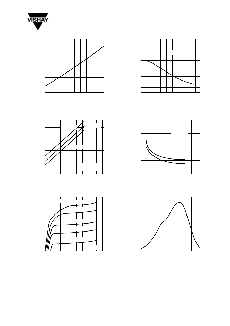
94 8239
0
0.6
0.8
1.0
1.2
1.4
2.0
I – Relative Collector Current
ca rel
20
40
60
80
T
amb
– Ambient Temperature (
°
C )
100
1.6
1.8
V
CE
=5V
E
e
=1mW/cm
2
l=950nm
Figure 3. Relative Collector Current vs.
Ambient Temperature
0.01
0.1
1
0.01
0.1
1
10
I – Collector Light Current ( mA
)
ca
E
e
– Irradiance ( mW / cm
2
)
10
94 8296
V
CE
=5V
l=950nm
BPW 96 A
BPW 96 B
BPW 96 C
Figure 4. Collector Light Current vs. Irradiance
0.1
1
10
0.1
1
10
I – Collector Light Current ( mA
)
ca
V
CE
– Collector Emitter Voltage ( V )
100
94 8297
E
e
=1 mW/cm
2
0.5 mW/cm
2
0.2 mW/cm
2
0.1 mW/cm
2
0.05 mW/cm
2
l=950nm
BPW 96 B
Figure 5. Collector Light Current vs.
Collector Emitter Voltage
0.1
1
10
0
2
4
6
8
10
V
CE
– Collector Emitter Voltage ( V )
100
94 8301
C – Collector Emitter Capacitance ( pF )
CEO
f=1MHz
Figure 6. Collector Emitter Capacitance vs.
Collector Emitter Voltage
0
2
4
6
12
0
2
8
14
94 8293
t / t –
T
urn on /
T
urn
of
f
T
ime ( s )
of
f
I
C
– Collector Current ( mA )
m
on
6
4
10
8
V
CE
=5V
R
L
=100
W
l=950nm
t
off
t
on
Figure 7. Turn On/Turn Off Time vs. Collector Current
400
600
1000
0
0.2
0.4
0.6
0.8
1.0
S ( ) – Relative Spectral Sensitivity
rel
l – Wavelength ( nm )
94 8348
l
800
Figure 8. Relative Spectral Sensitivity vs. Wavelength
BPW96
Vishay Telefunken
4 (6)
Rev. 3, 16-Nov-99
www.vishay.de
•
FaxBack +1-408-970-5600
Document Number 81532
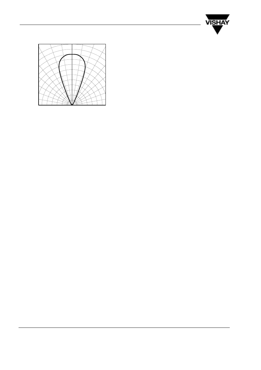
0.4
0.2
0
0.2
0.4
S – Relative Sensitivity
rel
0.6
94 8299
0.6
0.9
0.8
0
°
30
°
10
°
20
°
40
°
50
°
60
°
70
°
80
°
0.7
1.0
Figure 9. Relative Radiant Sensitivity vs.
Angular Displacement
BPW96
Vishay Telefunken
5 (6)
Rev. 3, 16-Nov-99
www.vishay.de
•
FaxBack +1-408-970-5600
Document Number 81532
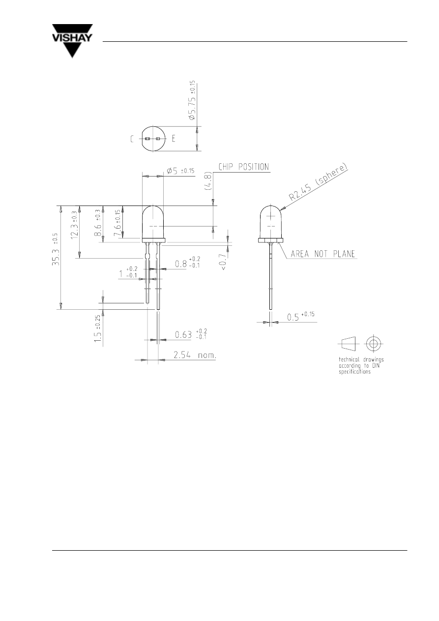
Dimensions in mm
96 12192

BPW96
Vishay Telefunken
6 (6)
Rev. 3, 16-Nov-99
www.vishay.de
•
FaxBack +1-408-970-5600
Document Number 81532
Ozone Depleting Substances Policy Statement
It is the policy of Vishay Semiconductor GmbH to
1. Meet all present and future national and international statutory requirements.
2. Regularly and continuously improve the performance of our products, processes, distribution and operating
systems with respect to their impact on the health and safety of our employees and the public, as well as their
impact on the environment.
It is particular concern to control or eliminate releases of those substances into the atmosphere which are known as
ozone depleting substances ( ODSs ).
The Montreal Protocol ( 1987 ) and its London Amendments ( 1990 ) intend to severely restrict the use of ODSs and
forbid their use within the next ten years. Various national and international initiatives are pressing for an earlier ban
on these substances.
Vishay Semiconductor GmbH has been able to use its policy of continuous improvements to eliminate the use of
ODSs listed in the following documents.
1. Annex A, B and list of transitional substances of the Montreal Protocol and the London Amendments respectively
2 . Class I and II ozone depleting substances in the Clean Air Act Amendments of 1990 by the Environmental
Protection Agency ( EPA ) in the USA
3. Council Decision 88/540/EEC and 91/690/EEC Annex A, B and C ( transitional substances ) respectively.
Vishay Semiconductor GmbH can certify that our semiconductors are not manufactured with ozone depleting
substances and do not contain such substances.
We reserve the right to make changes to improve technical design and may do so without further notice.
Parameters can vary in different applications. All operating parameters must be validated for each customer application
by the customer. Should the buyer use Vishay-Telefunken products for any unintended or unauthorized application, the
buyer shall indemnify Vishay-Telefunken against all claims, costs, damages, and expenses, arising out of, directly or
indirectly, any claim of personal damage, injury or death associated with such unintended or unauthorized use.
Vishay Semiconductor GmbH, P.O.B. 3535, D-74025 Heilbronn, Germany
Telephone: 49 ( 0 ) 7131 67 2831, Fax number: 49 ( 0 ) 7131 67 2423
Wyszukiwarka
Podobne podstrony:
BYV27 50 BYV27 200 (Vishay)
BF970 Vishay elenota pl
BF966S (Vishay)
BZX79 x2V4 x75 (Vishay)
SFH628A, SFH6286 (Vishay)
Si3430DV (Vishay)
XT26T (Vishay)
SUP40N25 60 (Vishay)
Vishay LTO 50
SFH615A, SFH6156 (Vishay)
XT49M (Vishay)
SFH617A [Vishay]
SUB65P06 20, SUP65P06 20 (Vishay)
MOC8050 (Vishay)
TCZT8020 (Vishay)
SFH618x (Vishay)
XO 523 (Vishay)
TSOP17xx (Vishay)
więcej podobnych podstron